EP1930969A2 - Lichtemittierendes Element, lichtemittierende Vorrichtung und elektronische Vorrichtung - Google Patents
Lichtemittierendes Element, lichtemittierende Vorrichtung und elektronische Vorrichtung Download PDFInfo
- Publication number
- EP1930969A2 EP1930969A2 EP07023467A EP07023467A EP1930969A2 EP 1930969 A2 EP1930969 A2 EP 1930969A2 EP 07023467 A EP07023467 A EP 07023467A EP 07023467 A EP07023467 A EP 07023467A EP 1930969 A2 EP1930969 A2 EP 1930969A2
- Authority
- EP
- European Patent Office
- Prior art keywords
- layer
- light emitting
- organic compound
- emitting device
- compound
- Prior art date
- Legal status (The legal status is an assumption and is not a legal conclusion. Google has not performed a legal analysis and makes no representation as to the accuracy of the status listed.)
- Granted
Links
Images






Classifications
-
- H—ELECTRICITY
- H05—ELECTRIC TECHNIQUES NOT OTHERWISE PROVIDED FOR
- H05B—ELECTRIC HEATING; ELECTRIC LIGHT SOURCES NOT OTHERWISE PROVIDED FOR; CIRCUIT ARRANGEMENTS FOR ELECTRIC LIGHT SOURCES, IN GENERAL
- H05B33/00—Electroluminescent light sources
- H05B33/12—Light sources with substantially two-dimensional [2D] radiating surfaces
- H05B33/14—Light sources with substantially two-dimensional [2D] radiating surfaces characterised by the chemical or physical composition or the arrangement of the electroluminescent material, or by the simultaneous addition of the electroluminescent material in or onto the light source
-
- C—CHEMISTRY; METALLURGY
- C09—DYES; PAINTS; POLISHES; NATURAL RESINS; ADHESIVES; COMPOSITIONS NOT OTHERWISE PROVIDED FOR; APPLICATIONS OF MATERIALS NOT OTHERWISE PROVIDED FOR
- C09K—MATERIALS FOR MISCELLANEOUS APPLICATIONS, NOT PROVIDED FOR ELSEWHERE
- C09K11/00—Luminescent materials, e.g. electroluminescent or chemiluminescent
- C09K11/06—Luminescent materials, e.g. electroluminescent or chemiluminescent containing organic luminescent materials
-
- H—ELECTRICITY
- H10—SEMICONDUCTOR DEVICES; ELECTRIC SOLID-STATE DEVICES NOT OTHERWISE PROVIDED FOR
- H10K—ORGANIC ELECTRIC SOLID-STATE DEVICES
- H10K50/00—Organic light-emitting devices
-
- H—ELECTRICITY
- H10—SEMICONDUCTOR DEVICES; ELECTRIC SOLID-STATE DEVICES NOT OTHERWISE PROVIDED FOR
- H10K—ORGANIC ELECTRIC SOLID-STATE DEVICES
- H10K50/00—Organic light-emitting devices
- H10K50/10—OLEDs or polymer light-emitting diodes [PLED]
- H10K50/11—OLEDs or polymer light-emitting diodes [PLED] characterised by the electroluminescent [EL] layers
-
- H—ELECTRICITY
- H10—SEMICONDUCTOR DEVICES; ELECTRIC SOLID-STATE DEVICES NOT OTHERWISE PROVIDED FOR
- H10K—ORGANIC ELECTRIC SOLID-STATE DEVICES
- H10K50/00—Organic light-emitting devices
- H10K50/10—OLEDs or polymer light-emitting diodes [PLED]
- H10K50/11—OLEDs or polymer light-emitting diodes [PLED] characterised by the electroluminescent [EL] layers
- H10K50/125—OLEDs or polymer light-emitting diodes [PLED] characterised by the electroluminescent [EL] layers specially adapted for multicolour light emission, e.g. for emitting white light
-
- H—ELECTRICITY
- H10—SEMICONDUCTOR DEVICES; ELECTRIC SOLID-STATE DEVICES NOT OTHERWISE PROVIDED FOR
- H10K—ORGANIC ELECTRIC SOLID-STATE DEVICES
- H10K50/00—Organic light-emitting devices
- H10K50/10—OLEDs or polymer light-emitting diodes [PLED]
- H10K50/14—Carrier transporting layers
- H10K50/15—Hole transporting layers
- H10K50/155—Hole transporting layers comprising dopants
-
- H—ELECTRICITY
- H10—SEMICONDUCTOR DEVICES; ELECTRIC SOLID-STATE DEVICES NOT OTHERWISE PROVIDED FOR
- H10K—ORGANIC ELECTRIC SOLID-STATE DEVICES
- H10K50/00—Organic light-emitting devices
- H10K50/10—OLEDs or polymer light-emitting diodes [PLED]
- H10K50/14—Carrier transporting layers
- H10K50/16—Electron transporting layers
- H10K50/165—Electron transporting layers comprising dopants
-
- H—ELECTRICITY
- H10—SEMICONDUCTOR DEVICES; ELECTRIC SOLID-STATE DEVICES NOT OTHERWISE PROVIDED FOR
- H10K—ORGANIC ELECTRIC SOLID-STATE DEVICES
- H10K85/00—Organic materials used in the body or electrodes of devices covered by this subclass
- H10K85/10—Organic polymers or oligomers
- H10K85/111—Organic polymers or oligomers comprising aromatic, heteroaromatic, or aryl chains, e.g. polyaniline, polyphenylene or polyphenylene vinylene
- H10K85/114—Poly-phenylenevinylene; Derivatives thereof
-
- H—ELECTRICITY
- H10—SEMICONDUCTOR DEVICES; ELECTRIC SOLID-STATE DEVICES NOT OTHERWISE PROVIDED FOR
- H10K—ORGANIC ELECTRIC SOLID-STATE DEVICES
- H10K2101/00—Properties of the organic materials covered by group H10K85/00
- H10K2101/40—Interrelation of parameters between multiple constituent active layers or sublayers, e.g. HOMO values in adjacent layers
-
- H—ELECTRICITY
- H10—SEMICONDUCTOR DEVICES; ELECTRIC SOLID-STATE DEVICES NOT OTHERWISE PROVIDED FOR
- H10K—ORGANIC ELECTRIC SOLID-STATE DEVICES
- H10K30/00—Organic devices sensitive to infrared radiation, light, electromagnetic radiation of shorter wavelength or corpuscular radiation
- H10K30/80—Constructional details
- H10K30/865—Intermediate layers comprising a mixture of materials of the adjoining active layers
-
- H—ELECTRICITY
- H10—SEMICONDUCTOR DEVICES; ELECTRIC SOLID-STATE DEVICES NOT OTHERWISE PROVIDED FOR
- H10K—ORGANIC ELECTRIC SOLID-STATE DEVICES
- H10K85/00—Organic materials used in the body or electrodes of devices covered by this subclass
- H10K85/10—Organic polymers or oligomers
- H10K85/111—Organic polymers or oligomers comprising aromatic, heteroaromatic, or aryl chains, e.g. polyaniline, polyphenylene or polyphenylene vinylene
-
- H—ELECTRICITY
- H10—SEMICONDUCTOR DEVICES; ELECTRIC SOLID-STATE DEVICES NOT OTHERWISE PROVIDED FOR
- H10K—ORGANIC ELECTRIC SOLID-STATE DEVICES
- H10K85/00—Organic materials used in the body or electrodes of devices covered by this subclass
- H10K85/10—Organic polymers or oligomers
- H10K85/111—Organic polymers or oligomers comprising aromatic, heteroaromatic, or aryl chains, e.g. polyaniline, polyphenylene or polyphenylene vinylene
- H10K85/115—Polyfluorene; Derivatives thereof
-
- H—ELECTRICITY
- H10—SEMICONDUCTOR DEVICES; ELECTRIC SOLID-STATE DEVICES NOT OTHERWISE PROVIDED FOR
- H10K—ORGANIC ELECTRIC SOLID-STATE DEVICES
- H10K85/00—Organic materials used in the body or electrodes of devices covered by this subclass
- H10K85/10—Organic polymers or oligomers
- H10K85/141—Organic polymers or oligomers comprising aliphatic or olefinic chains, e.g. poly N-vinylcarbazol, PVC or PTFE
- H10K85/146—Organic polymers or oligomers comprising aliphatic or olefinic chains, e.g. poly N-vinylcarbazol, PVC or PTFE poly N-vinylcarbazol; Derivatives thereof
-
- H—ELECTRICITY
- H10—SEMICONDUCTOR DEVICES; ELECTRIC SOLID-STATE DEVICES NOT OTHERWISE PROVIDED FOR
- H10K—ORGANIC ELECTRIC SOLID-STATE DEVICES
- H10K85/00—Organic materials used in the body or electrodes of devices covered by this subclass
- H10K85/10—Organic polymers or oligomers
- H10K85/151—Copolymers
Definitions
- the present invention relates to a current excitation type light emitting element.
- the present invention relates to a light emitting device and an electronic device having the light emitting element.
- the light emitting element Since such a light emitting element is of self light emitting type, it is considered that the light emitting element has advantages over a liquid crystal display in that visibility of pixels is high, backlight is not required, and so on and is therefore suitable as a flat panel display element. In addition, other advantages of such a light emitting element are that the element can be manufactured to be thin and lightweight and the response speed is very high.
- the light emitting element can be formed into a film shape, surface light emission can be easily obtained by forming a large-area element. This is a feature which is difficult to be obtained by point light sources typified by an incandescent lamp and an LED or linear light sources typified by a fluorescent lamp. Accordingly, the light emitting element is extremely effective for use as a surface light source applicable to illumination and the like.
- Light emitting elements using electroluminescence are classified broadly according to whether they use an organic compound or an inorganic compound as a light emitting substance.
- an organic compound When an organic compound is used as a light emitting substance, electrons and holes are injected into a layer including a light emitting organic compound from a pair of electrodes by voltage application to a light emitting element, so that a current flows therethrough.
- the electrons and holes i.e., carriers
- the light emitting organic compound becomes in an excited state.
- the light emitting organic compound returns to a ground state from the excited state, thereby emitting light. Based on this mechanism, such a light emitting element is called a current excitation type light emitting element.
- the excited state of an organic compound can be a singlet excited state or a triplet excited state, and luminescence from the singlet excited state is referred to as fluorescence, and luminescence from the triplet excited state is referred to as phosphorescence.
- Reference 1 describes a light emitting element in which a guest substance is dispersed in the whole organic function layer between electrodes to enhance the possibility of injection and recombination of electrons and holes for light emission.
- Reference 1 does not refer to a lifetime of the light emitting element (Reference 1: Japanese Published Patent Application No. H 6-158038 ).
- Such a light emitting element including a light emitting organic compound can be driven at lower voltage than a light emitting element using a light emitting inorganic compound; however, such a light emitting element including a light emitting organic compound has a problem of having a short lifetime. Thus, a light emitting element with a longer lifetime is desired.
- a substantial light emitting region of a light emitting layer is set in the vicinity of the center of the light emitting layer in a light emitting element.
- a light emitting layer is constituted by a combination of layers having different carrier transporting properties so that the light emitting region is set in the vicinity of the center of the light emitting layer, not at the interface between the light emitting layer and a hole transporting layer or at the interface between the light emitting layer and an electron transporting layer.
- an aspect of the present invention is a light emitting element comprising an electron transporting layer and a hole transporting layer between a first electrode and a second electrode, and a first layer and a second layer between the electron transporting layer and the hole transporting layer.
- the first layer includes a first organic compound and an organic compound having a hole transporting property
- the second layer includes a second organic compound and an organic compound having an electron transporting property
- the first layer is formed in contact with the first electrode side of the second layer, at least one of either the organic compound having a hole transporting property and the organic compound having an electron transporting property is a high molecular compound
- the first organic compound and the second organic compound are the same compound and a voltage is applied to the first electrode and the second electrode so that a potential of the first electrode is higher than that of the second electrode, thereby making the first organic compound and the second organic compound emit light.
- the present invention is a light emitting element comprising an electron transporting layer and a hole transporting layer between a first electrode and a second electrode, and a first layer and a second layer between the electron transporting layer and the hole transporting layer.
- the first layer includes a first organic compound and an organic compound having a hole transporting property, the highest occupied molecular orbital level (HOMO level) of the organic compound having a hole transporting property is greater than or equal to -6.0 eV and less than or equal to -5.0 eV, and the lowest unoccupied molecular orbital level (LUMO level) of the organic compound having a hole transporting property is greater than or equal to -3.0 eV and less than or equal to -2.0 eV
- the second layer includes a second organic compound and an organic compound having an electron transporting property, the highest occupied molecular orbital level (HOMO level) of the organic compound having an electron transporting property is greater than or equal to -6.0 eV and less than or equal to -5.0 e
- Another aspect of the present invention is a light emitting element comprising an electron transporting layer and a hole transporting layer between a first electrode and a second electrode, and a first layer and a second layer between the electron transporting layer and the hole transporting layer.
- the first layer includes a first organic compound and an organic compound having a hole transporting property
- the second layer includes a second organic compound and an organic compound having an electron transporting property
- the first layer is formed in contact with the first electrode side of the second layer
- a difference between the highest occupied molecular orbital level of the organic compound having a hole transporting property and the highest occupied molecular orbital level of the organic compound having an electron transporting property is 0.3 eV or less
- a difference between the lowest unoccupied molecular orbital level of the organic compound having a hole transporting property and the lowest unoccupied molecular orbital level of the organic compound having an electron transporting property is 0.3 eV or less
- Another aspect of the present invention is a light emitting element comprising a light emitting layer between a first electrode and a second electrode, and a first layer and a second layer included in the light emitting layer.
- the first layer includes a first organic compound and an organic compound having a hole transporting property
- the second layer includes a second organic compound and an organic compound having an electron transporting property
- the first layer is formed in contact with the first electrode side of the second layer, at least one of either the organic compound having a hole transporting property and the organic compound having an electron transporting property is a high molecular compound
- the first organic compound and the second organic compound are the same compound and a voltage is applied to the first electrode and the second electrode so that a potential of the first electrode is higher than that of the second electrode, thereby making the first organic compound and the second organic compound emit light.
- the present invention is a light emitting element comprising a light emitting layer between a first electrode and a second electrode, and a first layer and a second layer included in the light emitting layer.
- the first layer includes a first organic compound and an organic compound having a hole transporting property, the highest occupied molecular orbital level (HOMO level) of the organic compound having a hole transporting property is greater than or equal to -6.0 eV and less than or equal to -5.0 eV, and the lowest unoccupied molecular orbital level (LUMO level) of the organic compound having a hole transporting property is greater than or equal to -3.0 eV and less than or equal to -2.0 eV
- the second layer includes a second organic compound and an organic compound having an electron transporting property, the highest occupied molecular orbital level (HOMO level) of the organic compound having an electron transporting property is greater than or equal to -6.0 eV and less than or equal to -5.0 eV, and the lowest unoccupied molecular orbit
- Another aspect of the present invention is a light emitting element comprising a light emitting layer between a first electrode and a second electrode, and a first layer and a second layer included in the light emitting layer.
- the first layer includes a first organic compound and an organic compound having a hole transporting property
- the second layer includes a second organic compound and an organic compound having an electron transporting property
- the first layer is formed in contact with the first electrode side of the second layer, a difference between the highest occupied molecular orbital level of the organic compound having a hole transporting property and the highest occupied molecular orbital level of the organic compound having an electron transporting property is 0.3 eV or less
- a difference between the lowest unoccupied molecular orbital level of the organic compound having a hole transporting property and the lowest unoccupied molecular orbital level of the organic compound having an electron transporting property is 0.3 eV or less
- at least one of either the organic compound having a hole transporting property and the organic compound having an electron transporting property is a high mo
- the present invention also includes a light emitting device having the above-described light emitting element in its category.
- the light emitting device in this specification includes image display devices, light emitting devices, and light sources (including illumination devices). Further, the light emitting device includes all of the following modules: modules in which a connector such as an FPC (flexible printed circuit), a TAB (tape automated bonding) tape, or a TCP (tape carrier package) is attached to a panel in which a light emitting element is formed; modules having a TAB tape or a TCP provided with a printed wiring board at the end thereof; and modules having an IC (integrated circuit) directly mounted on a light emitting element by a COG (chip on glass) method.
- a connector such as an FPC (flexible printed circuit), a TAB (tape automated bonding) tape, or a TCP (tape carrier package) is attached to a panel in which a light emitting element is formed
- an electronic device using the light emitting element of the present invention in its display portion is also included in the category of the present invention. Therefore, one feature of the electronic device of the present invention is to include a display portion where the aforementioned light emitting element and a controller for controlling light emission of the light emitting element are equipped.
- a light emitting region is formed in the vicinity of the center of a light emitting layer, not at the interface between the light emitting layer and a hole transporting layer or at the interface between the light emitting layer and an electron transporting layer, and thus, the light emitting element does not deteriorate very much. In other words, the change of luminance over time is small and a light emitting element having a long lifetime can be provided.
- a light emitting element of the present invention is applied to light emitting devices and electronic devices, so that the light emitting devices and the electronic devices can have long lifetimes.
- composite means not only a state in which two materials are simply mixed but also a state in which a plurality of materials are mixed and charges are transferred between the materials.
- the light emitting element of the present invention includes a plurality of layers between a pair of electrodes.
- the plurality of layers are stacked by a combination of layers including a substance with a high carrier injecting property and a substance with a high carrier transporting property so that a light emitting region is formed apart from the electrodes, in other words, recombination of carriers is performed in a portion apart from the electrodes.
- the light emitting element includes a first electrode 102, a second electrode 104, and an EL layer 103 formed between the first electrode 102 and the second electrode 104.
- description in this embodiment mode is carried out on the assumption that the first electrode 102 serves as an anode and the second electrode 104 serves as a cathode.
- description is hereinafter carried out on the assumption that light emission can be obtained when a voltage is applied to the first electrode 102 and the second electrode 104 so that a potential of the first electrode 102 is higher than that of the second electrode 104.
- the substrate 101 is used as a support of the light emitting element.
- glass, plastic, or the like can be used, for example. Note that materials other than glass and plastic can be used as long as they can function as a support in a manufacturing process of a light emitting element.
- the first electrode 102 is preferably formed of a metal, an alloy, a conductive compound, a mixture of these, or the like each having a high work function (specifically, a work function of 4.0 eV or higher).
- a high work function specifically, a work function of 4.0 eV or higher.
- ITO indium oxide-tin oxide
- IZO indium zinc oxide
- IWZO indium oxide including tungsten oxide and zinc oxide
- films of these conductive metal oxides are usually formed by sputtering; however, a sol-gel method or the like may also be used.
- indium oxide-zinc oxide can be formed by a sputtering method using a target in which 1 to 20 wt% of zinc oxide with respect to indium oxide is included.
- indium oxide (IWZO) including tungsten oxide and zinc oxide can be formed by a sputtering method using a target in which 0.5 to 5 wt% of tungsten oxide and 0.1 to 1 wt% of zinc oxide with respect to indium oxide are included.
- gold Au
- platinum Pt
- nickel Ni
- tungsten W
- Cr chromium
- Mo molybdenum
- iron Fe
- Co cobalt
- Cu copper
- palladium Pd
- a nitride of a metal material such as titanium nitride
- various metals, alloys, electrically conductive compounds, mixtures thereof, or the like can be used for the first electrode regardless of the work function.
- aluminum (Al), silver (Ag), an alloy containing aluminum (e.g., AlSi), or the like can be used.
- an element belonging to Group 1 or Group 2 in the periodic table which is a low function material, in other words, an alkali metal such as lithium (Li) or cesium (Cs), an alkaline earth metal such as magnesium (Mg), calcium (Ca), or strontium (Sr), an alloy including these elements (e..g., MgAg, AlLi), a rare earth metal such as europium (Eu) or ytterbium (Yb), an alloy including such rare earth metals, or the like can be used.
- a film of an alkali metal, an alkaline earth metal, or an alloy including these can be formed by a vacuum evaporation method.
- a film of an alloy including an alkali metal or an alkaline earth metal can also be formed by a sputtering method.
- a silver paste or the like can be used to form a film, using an inkjet method or the like.
- FIGS. 1A to 1C show examples in which the first electrode 102, a hole transporting layer 112, a light emitting layer 111, an electron transporting layer 113, and the second electrode 104 are sequentially stacked.
- a hole injecting layer may be formed between the first electrode 102 and the hole transporting layer 112.
- the hole injecting layer is a layer having a substance with a high hole injecting property.
- the substance with a high hole injecting property molybdenum oxide, vanadium oxide, ruthenium oxide, tungsten oxide, manganese oxide, or the like may be used.
- a phthalocyanine-based compound such as phthalocyanine (H 2 Pc) or copper phthalocyanine (CuPc)
- a high molecule such as poly(3,4-ethylenedioxythiophene)/poly(styrenesufonate) (PEDOT/PSS), or the like to form the hole injecting layer.
- a composite material in which an acceptor substance is mixed into a substance with a high hole transporting property can be used as the hole injecting layer. It is to be noted that, by using such a composite material in which an acceptor substance is mixed into a substance with a high hole transporting property, a material for forming an electrode can be selected regardless of the work function. In other words, besides a material with a high work function, a material with a low work function may also be used for the first electrode 102.
- the acceptor substance 7,7,8,8-tetracyano-2,3,5,6-tetrafluoroquinodimethane (abbr.: F 4 -TCNQ), chloranil, and the like can be given.
- a transition metal oxide can be given.
- oxides of metals that belong to Group 4 to Group 8 in the periodic table can be given.
- vanadium oxide, niobium oxide, tantalum oxide, chromium oxide, molybdenum oxide, tungsten oxide, manganese oxide, and rhenium oxide are preferable since their electron accepting properties are high.
- molybdenum oxide is especially preferable since it is stable in the air, has a low hygroscopic property, and is easily treated.
- organic compound used for the composite material various compounds such as an aromatic amine compound, carbazole derivatives, aromatic hydrocarbon, and a high molecular compound (such as oligomer, dendrimer, or polymer) can be used.
- the organic compound used for the composite material is preferably an organic compound having a high hole transporting property. Specifically, a substance having a hole mobility of 10 -6 cm 2 /Vs or higher is preferably used. However, other substances than the above-described materials may also be used as long as the substances have higher hole transporting properties than electron transporting properties.
- the organic compounds which can be used for the composite material will be specifically shown below.
- the aromatic amine compound 4,4'-bis[ N -(1-naphthyl)- N -phenylamino]biphenyl (abbr.: NPB); N,N' -bis(3-methylphenyl)- N,N' -diphenyl-[1,1'-biphenyl]-4,4'-diamine (abbr.: TPD); 4,4',4"-tris( N,N -diphenylamino)triphenylamine (abbr.: TDATA); 4,4',4"-tris[ N -(3-methylphenyl)- N -phenylamino]triphenylamine (abbr.: MTDATA); 4,4'-bis[ N -(spiro-9,9'-bifluoren-2-yl)- N -phenylamino]biphenyl (abbr.: BSPB); and the like.
- NPB N,N' -bis(3-methylphenyl
- N N '-bis(4-methylphenyl)( p -tolyl)- N , N '-diphenyl- p -phenylenediamine
- DTDPPA 4,4'-bis[ N -(4-diphenylaminophenyl)- N -phenylamino]biphenyl
- DPAB 4,4'-bis( N - ⁇ 4-[ N' -(3-methylphenyl)- N '-phenylamino]phenyl ⁇ - N -phenylamino)biphenyl
- DNTPD 1,3,5-tris[ N -(4-diphenylaminophenyl)- N -phenylamino]benzene
- DPA3B 1,3,5-tris[ N -(4-diphenylaminophenyl)- N -phenylamino]benzene
- carbazole derivatives which can be used for the composite material, the following can be given specifically: 3-[ N -(9-phenylcarbazol-3-yl)- N -phenylamino]-9-phenylcarbazole (abbr.: PCzPCAl); 3,6-bis[ N -(9-phenylcarbazol-3-yl)- N -phenylamino]-9-phenylcarbazole (abbr.: PCzPCA2); 3-[ N -(1-naphthyl)- N -(9-phenylcarbazol-3-yl)amino]-9-phenylcarbazole (abbr.: PCzPCN1); and the like.
- carbazole derivatives which can be used for the composite material, 4,4'-di( N -carbazolyl)biphenyl (abbr.: CBP); 1,3,5-tris[4-( N -carbazolyl)phenyl]benzene (abbr.: TCPB); 9-[4-(10-phenyl-9-anthryl)phenyl]-9 H -carbazole (abbr.: CzPA); 1,4-bis[4-( N -carbazolyl)phenyl]-2,3,5,6-tetraphenylbenzene; or the like can also be used.
- CBP 4,4'-di( N -carbazolyl)biphenyl
- TCPB 1,3,5-tris[4-( N -carbazolyl)phenyl]benzene
- CzPA 9-[4-(10-phenyl-9-anthryl)phenyl]-9 H -carbazole
- aromatic hydrocarbon which can be used for the composite material, the following can be given for example: 2- tert -butyl-9,10-di(2-naphthyl)anthracene (abbr.: t -BuDNA); 2- tert -butyl-9,10-di(1-naphthyl)anthracene, 9,10-bis(3,5-diphenylphenyl)anthracene (abbr.: DPPA); 2- tert -butyl-9,10-bis(4-phenylphenyl)anthracene (abbr.: t -BuDBA); 9,10-di(2-naphthyl)anthracene (abbr.: DNA); 9,10-diphenylanthracene (abbr.: DPAnth); 2- tert -butylanthracene (abbr.: t -BuAnth); 9,10-bis(4-methyl-1-nap
- the aromatic hydrocarbon which can be used for the composite material may have a vinyl skeleton.
- the aromatic hydrocarbon having a vinyl group the following are given for example: 4,4'-bis(2,2-diphenylvinyl)biphenyl (abbr.: DPVBi); 9,10-bis[4-(2,2-diphenylvinyl)phenyl]anthracene (abbr.: DPVPA); and the like.
- a high molecular compound such as poly( N -vinylcarbazole) (abbr.: PVK), poly(4-vinyltriphenylamine) (abbr.: PVTPA), poly[ N -(4- ⁇ N '-[4-(4-diphenylamino)phenyl]phenyl- N '-phenylamino ⁇ phenyl)methacryla mide] (abbr.: PTPDMA), or poly[ N,N' -bis(4-butylphenyl)- N,N' -bis(phenyl)benzidine (abbr.: poly-TPD) can also be used.
- PVK poly( N -vinylcarbazole)
- PVTPA poly(4-vinyltriphenylamine)
- PVTPA poly[ N -(4- ⁇ N '-[4-(4-diphenylamino)phenyl]phenyl- N '-phenylamino ⁇ phenyl
- the hole transporting layer 112 is a layer that contains a substance with a high hole transporting property.
- a substance with a high hole transporting property for example, an aromatic amine compound such as 4,4'-bis[ N -(1-naphthyl)- N -phenylamino]biphenyl (abbr.: NPB or ⁇ -NPD), N , N' -bis(3-methylphenyl)- N , N '-diphenyl-[1,1'-biphenyl]-4,4'-diamine (abbr.: TPD), 4,4',4"-tris( N , N -diphenylamino)triphenylamine (abbr.: TDATA), 4,4',4"-tris[ N -(3-methylphenyl)- N -phenylamino]triphenylamine (abbr.: MTDATA), or 4,4'-bis[ N -(spiro-9,9 ' -b
- These substances are mainly substances each having a hole mobility of 10- 6 cm 2 /Vs or higher. However, other substances than these substances may also be used as long as the substances have hole transporting properties higher than electron transporting properties.
- the layer containing a substance with a high hole transporting property is not limited to a single layer, and two or more layers containing the aforementioned substances may be stacked.
- a high molecular compound such as poly( N- vinylcarbazole) (abbr.: PVK) or poly(4-vinyltriphenylamine) (abbr.: PVTPA) can also be used for the hole transporting layer.
- PVK poly( N- vinylcarbazole)
- PVTPA poly(4-vinyltriphenylamine)
- the light emitting layer 111 is a layer including a substance having a high light emitting property.
- the light emitting layer includes a first layer 121 and a second layer 122.
- the first layer 121 includes a first organic compound and an organic compound having a hole transporting property
- the second layer 122 includes the first organic compound and an organic compound having an electron transporting property.
- the first layer is provided on the first electrode side of the second layer, in other words, on the anode side of the second layer.
- the first organic compound and the second organic compound is a substance having a high light emitting property, and various materials can be used. Specifically, the following materials can be used: such as N,N -dimethylquinacridone (abbr.: DMQd); N , N '-diphenylquinacridone (abbr.: DPQd); coumarin 6; coumarin 545T; (2- ⁇ 2-[4-(dimethylamino)phenyl]ethenyl ⁇ -6-methyl-4 H -pyran-4-ylidene)propanedinitril e (abbr.: DCM1); ⁇ 2-methyl-6-[2-(2,3,6,7-tetrahydro-1 H ,5 H -benzo[ ij ]quinolizin-9-yl)ethenyl]-4 H -pyran-4-ylidene ⁇ propanedinitrile (abbr.: DCM2); ⁇ 2-(1,1-dimethylethyl)-6-[
- the organic compound having a hole transporting property included in the first layer 121 is a substance which exhibits a hole transporting property higher than an electron transporting property.
- the organic compound having an electron transporting property included in the second layer 122 is a substance which exhibits an electron transporting property higher than a hole transporting property.
- FIG 10 shows an example of a band diagram of a light emitting element of the present invention illustrated in FIGS. 1A to 1C .
- holes injected from the first electrode 102 are injected into the first layer 121.
- the holes injected into the first layer 121 are transported through the first layer 121 and further injected into the second layer 122.
- the organic compound having an electron transporting property included in the second layer 122 is a substance which exhibits a higher electron transporting property than a hole transporting property, and thus, the holes injected into the second layer 122 become difficult to move. Consequently, a large number of holes are present near the interface between the first layer 121 and the second layer 122.
- occurrence of a phenomenon in which holes reach the electron transporting layer 113 without being recombined with electrons can be suppressed.
- electrons injected from the second electrode 104 are injected into the second layer 122.
- the electrons injected into the second layer 122 are transported through the second layer 122 and further injected into the first layer 121.
- the organic compound having a hole transporting property included in the first layer 121 is a substance which exhibits a higher hole transporting property than an electron transporting property, and thus, the electrons injected into the first layer 121 become difficult to move. Consequently, a large number of electrons are present near the interface between the first layer 121 and the second layer 122.
- occurrence of a phenomenon in which electrons reach the hole transporting layer 112 without being recombined with holes can be suppressed.
- the light emitting region is formed in the vicinity of the center of the light emitting layer 111.
- occurrence of a phenomenon in which holes reach the electron transporting layer 113 without being recombined with electrons or electrons reach the hole transporting layer 112 without being recombined with holes can be suppressed, so that reduction in recombination probability can be prevented.
- reduction of carrier balance over time can be prevented, which leads to improvement of reliability.
- the organic compound having a hole transporting property is an organic compound which can be oxidized and reduced.
- the highest occupied molecular orbital level (HOMO level) of the organic compound having a hole transporting property is preferably greater than or equal to -6.0 eV and less than or equal to -5.0 eV
- the lowest unoccupied molecular orbital level (LUMO level) of the organic compound having a hole transporting property is preferably greater than or equal to -3.0 eV and less than or equal to -2.0 eV.
- the organic compound having an electron transporting property is an organic compound which can be oxidized and reduced.
- the highest occupied molecular orbital level (HOMO level) of the organic compound having an electron transporting property is preferably greater than or equal to -6.0 eV and less than or equal to -5.0 eV.
- the lowest unoccupied molecular orbital level (LUMO level) of the organic compound having an electron transporting property is preferably greater than or equal to -3.0 eV and less than or equal to -2.0 eV.
- the light emitting element of the present invention is structured so that holes are injected into the second layer 122 from the first layer 121.
- the difference between the highest occupied molecular orbital level (HOMO level) of the organic compound having a hole transporting property and the highest occupied molecular orbital level (HOMO level) of the organic compound having an electron transporting property is preferably small.
- the light emitting element of the present invention is structured so that electrons are injected into the first layer 121 from the second layer 122.
- the difference between the lowest unoccupied molecular orbital level (LUMO level) of the organic compound having a hole transporting property and the lowest unoccupied molecular orbital level (LUMO level) of the organic compound having an electron transporting property is preferably small. If the difference between the HOMO level of the organic compound having a hole transporting property and the HOMO level of the organic compound having an electron transporting property is large, the light emitting region is formed more on the first layer side or the second layer side. Similarly, if the difference between the LUMO level of the organic compound having a hole transporting property and the LUMO level of the organic compound having an electron transporting property is large, the light emitting region is formed more on the first layer side or the second layer side.
- the difference between the highest occupied molecular orbital level (HOMO level) of the organic compound having a hole transporting property and the highest occupied molecular orbital level (HOMO level) of the organic compound having an electron transporting property is preferably 0.3 eV or less, and more preferably 0.1 eV or less.
- the difference between the lowest unoccupied molecular orbital level (LUMO level) of the organic compound having a hole transporting property and the lowest unoccupied molecular orbital level (LUMO level) of the organic compound having an electron transporting property is preferably 0.3 eV or less, and more preferably 0.1 eV or less.
- the light emitting element provides light emission by recombination of electrons and holes
- the organic compound used in the light emitting layer 111 is preferably stable even when an oxidative reaction and a reductive reaction are repeated.
- the organic compound is preferably reversible to the oxidative reaction and the reductive reaction.
- the organic compound having a hole transporting property and the organic compound having an electron transporting property are preferably stable even when an oxidative reaction and a reductive reaction are repeated. It can be confirmed by employing the cyclic voltammetry (CV) measurement whether the organic compounds are stable when an oxidative reaction and a reductive reaction are repeated.
- CV cyclic voltammetry
- the changes in the intensity of the oxidation peak potential and the intensity of the reduction peak potential are preferably less than 50 %, and more preferably less than 30 %.
- a peak intensity of 50 % or higher is preferably kept even when the oxidation peak potential decreases. More preferably, a peak intensity of 70 % or higher is kept.
- the changes of the values of the oxidation peak potential and the reduction peak potential are preferably 0.05 V or lower. More preferably, the changes are 0.02 V or lower.
- At least one of either the organic compound having a hole transporting property included in the first layer 121 and the organic compound having an electron transporting property included in the second layer 122 is a high molecular compound. Because of this, at least one of the first layer 121 and the second layer 122 can be formed by a wet process. Accordingly, in the case where the light emitting element of the present invention is applied to a display device such as a full-color display and separate coloring of light emitting layers is necessary, the separate coloring of the light emitting layers becomes easy and productivity is improved. In addition, since the material use efficiency is increased, cost reduction is possible.
- both the organic compound having a hole transporting property included in the first layer 121 and the organic compound having an electron transporting property included in the second layer 122 are high molecular compounds because the first layer 121 and the second layer 122 can be formed by a wet process.
- a high molecular compound such as poly( N -vinylcarbazole) (abbr.: PVK); poly(4-vinyltriphenylamine) (abbr.: PVTPA); poly[ N -(4- ⁇ N'-[4-(4-diphenylamino)phenyl]phenyl-N'-phenylamino ⁇ phenyl)methacryla mide] (abbr.: PTPDMA); or poly[N,N'-bis(4-butylphenyl)-N,N'-bis(phenyl)benzidine] (abbr.: Poly-TPD) can be used.
- PVK poly( N -vinylcarbazole)
- PVTPA poly(4-vinyltriphenylamine)
- PVTPA poly[ N -(4- ⁇ N'-[4-(4-diphenylamino)phenyl]phenyl-N'-phenylamino ⁇ phenyl)methacryla mid
- a high molecular compound such as poly[(9,9-dihexylfluorene-2,7-diyl)-co-(pyridin-3,5-diyl)] (abbr.: PF-Py) or poly[(9,9-dioctylfluorene-2,7-diyl)-co-(2,2'-bipyridin-6,6'-diyl)] (abbr.: PF-BPy) can be used.
- PF-Py poly[(9,9-dihexylfluorene-2,7-diyl)-co-(pyridin-3,5-diyl)]
- PF-BPy poly[(9,9-dioctylfluorene-2,7-diyl)-co-(2,2'-bipyridin-6,6'-diyl)]
- a high molecular compound such as the above-described PF-Py or PF-BPy is used as the organic compound having an electron transporting property included in the second layer 122
- a low molecular compound such as 9,10-diphenylanthracene (abbr.: DPAnth); N,N -diphenyl-9-[4-(10-phenyl-9-anthryl)phenyl]-9 H -carbazol-3-amine (abbr.: CzAIPA); 4-(10-phenyl-9-anthryl)triphenylamine (abbr.: DPhPA); N ,9-diphenyl- N -[4-(10-phenyl-9-anthryl)phenyl]-9 H -carbazol-3-amine (abbr.: PCAPA); N ,9-diphenyl- N - ⁇ 4-[
- the same substance is used for the substance having a high light emitting property included in the first layer and the substance having a high light emitting property included in the second layer, thereby making it possible to emit light in the vicinity of the center of the light emitting layer.
- the substance having a high light emitting property included in the first layer and the substance having a high light emitting property included in the second layer are preferably the same.
- the electron transporting layer 113 is a layer that contains a substance with a high electron transporting property.
- a layer containing a metal complex having a quinoline skeleton or a benzoquinoline skeleton such as tris(8-quinolinolato)aluminum (abbr.: Alq); tris(4-methyl-8-quinolinolato)aluminum (abbr.: Almq 3 ); bis(10-hydroxybenzo[ h ]-quinolinato)beryllium (abbr.: BeBq 2 ); or bis(2-methyl-8-quinolinolato)(4-phenylphenolato)aluminum (abbr.: BAlq), or the like can be used.
- a metal complex having an oxazole-based or thiazole-based ligand such as bis[2-(2-hydroxyphenyl)benzoxazolato]zinc (abbr.: Zn(BOX) 2 ) or bis[2-(2-hydroxyphenyl)benzothiazolato]zinc (abbr.: Zn(BTZ) 2 ), or the like can be used.
- 2-(4-biphenylyl)-5-(4- tert -butylphenyl)-1,3,4-oxadiazole (abbr.: PBD), 1,3-bis[5-( p - tert -butylphenyl)-1,3,4-oxadiazol-2-yl]benzene (abbr.: OXD-7), 3-(4-biphenylyl)-4-phenyl-5-(4- tert -butylphenyl)-1,2,4-triazole (abbr.: TAZ), bathophenanthroline (abbr.: BPhen), bathocuproine (abbr.: BCP), or the like can also be used.
- PBD 2-(4-biphenylyl)-5-(4- tert -butylphenyl)-1,3,4-oxadiazole
- OXD-7 1,3-bis[5-( p - tert -butylphenyl)
- the substances mentioned here are mainly materials each having an electron mobility of 10 -6 cm 2 /Vs or higher.
- the electron transporting layer may be formed of other materials than those described above as long as the materials have electron transporting properties higher than hole transporting properties.
- the electron transporting layer is not limited to a single layer, and two or more layers made of the aforementioned substances may be stacked.
- a high molecular compound for the electron transporting layer, a high molecular compound can be used.
- poly[(9,9-dihexylfluorene-2,7-diyl)-co-(pyridin-3,5-diyl)] abbreviations: PF-Py
- poly[(9,9-dioctylfluorene-2,7-diyl)-co-(2,2'-bipyridin-6,6'-diyl)] abbreviations: PF-BPy
- PF-BPy poly[(9,9-dioctylfluorene-2,7-diyl)-co-(2,2'-bipyridin-6,6'-diyl)]
- an electron injecting layer which includes a substance with a high electron injecting property, may be provided between the electron transporting layer 113 and the second electrode 104.
- an alkali metal, an alkaline earth metal, or a compound thereof such as lithium fluoride (LiF), cesium fluoride (CsF), or calcium fluoride (CaF 2 ) may be used.
- a layer of a substance having an electron transporting property containing an alkali metal, an alkaline earth metal, or a compound thereof, such as a layer of Alq which contains magnesium (Mg) may be used.
- a film of an alkali metal, an alkaline earth metal, or an alloy thereof can be formed by a vacuum evaporation method.
- a film of an alloy including an alkali metal or an alkaline earth metal can also be formed by a sputtering method. Further, a silver paste or the like can also be used to form a film, using an inkjet method or the like.
- a layer of a substance having an electron transporting property, in which an alkali metal or an alkaline earth metal is contained, as the electron injecting layer electron injection from the second electrode 104 is performed efficiently, which is preferable.
- the second electrode 104 can be formed of a metal, an alloy, an electrically conductive compound, or a mixture of these, having a low work function (specifically, a work function of 3.8 eV or lower).
- a cathode material an element belonging to Group 1 or Group 2 in the periodic table, i.e., an alkali metal such as lithium (Li) or cesium (Cs), or an alkaline earth metal such as magnesium (Mg), calcium (Ca), or strontium (Sr); an alloy containing any of these (such as MgAg or AlLi); a rare earth metal such as europium (Er) or ytterbium (Yb); an alloy containing such a rare earth metal; or the like can be used.
- the second electrode 104 can be formed of various conductive materials such as Al, Ag, ITO, and indium oxide-tin oxide including silicon or silicon oxide regardless of its work function.
- a film of these conductive materials can be formed by a sputtering method, an inkjet method, a spin coating method, or the like.
- a formation method of the EL layer various methods can be employed regardless of a wet process or a dry process. For example, a vacuum evaporation method, an inkjet method, a spin coating method, or the like may be used. A different formation method may be employed for each electrode or each layer.
- a layer that uses a high molecular compound in particular, the first layer 121 or the second layer 122
- a wet process may be employed, or a dry process such as a vacuum evaporation method may also be employed.
- the electrodes may be formed by a sol-gel method, which is a wet process, or may also be formed by a wet process using a paste of a metal material.
- a dry process such as a sputtering method or a vacuum evaporation method may also be employed.
- a specific formation method of a light emitting element will be described.
- a light emitting element of the present invention is applied to a display device and separate coloring of light emitting layers is carried out, it is preferable to form the light emitting layers by a wet process.
- a wet process such as an inkjet method, separate coloring of the light emitting layers becomes easy even when a large substrate is used.
- the first electrode may be formed by a sputtering method, which is a dry process; the hole injecting layer may be formed by an inkjet method or a spin coating method, which are wet processes; the hole transporting layer may be formed by a vacuum evaporation method, which is a dry process; the first layer may be formed by an inkjet method, which is a wet process; the second layer may be formed by a co-evaporation method, which is a dry process; the electron transporting layer and the electron injecting layer may be formed by a vacuum evaporation method, which is a dry process; and the second electrode may be formed by an inkjet method or a spin coating method, which are wet processes.
- the first electrode may be formed by an inkjet method, which is a wet process; the hole injecting layer may be formed by a vacuum evaporation method, which is a dry process; the hole transporting layer may be formed by an inkjet method or a spin coating method, which are wet processes; the first layer may be formed by an inkjet method, which is a wet process; the second layer may be formed by an inkjet method or a spin coating method, which are wet processes; the electron transporting layer and the electron injecting layer may be formed by an inkjet method or a spin coating method, which are wet processes; and the second electrode may be formed by an inkjet method or a spin coating method, which are wet processes.
- a wet process and a dry process may be appropriately combined.
- the first electrode can be formed by a sputtering method, which is a dry process; the hole injecting layer and the hole transporting layer can be formed by an inkjet method or a spin coating method, which are wet processes; the first layer can be formed by an inkjet method, which is a wet process; the second layer can be formed by a co-evaporation method, which is a dry process; the electron transporting layer and the electron injecting layer can be formed by a vacuum evaporation method, which is a dry process; and the second electrode can be formed by a vacuum evaporation method, which is a dry process.
- the hole injecting layer to the first layer can be formed by a wet process, and the second layer to the second electrode can be formed by a dry process.
- the hole injecting layer to the first layer can be formed at atmospheric pressure and separate coloring for the first layer is easy.
- the second layer to the second electrode can be formed in vacuum consistently. Therefore, the process can be simplified and productivity can be improved.
- the second electrode can be formed by a sputtering method or a vacuum evaporation method, which are dry processes;
- the electron injecting layer to the electron transporting layer can be formed by a vacuum evaporation method, which is a dry process;
- the second layer can be formed by a co-evaporation method;
- the first layer can be formed by an inkjet method, which is a wet process;
- the hole transporting layer and the hole injecting layer can be formed by an inkjet method or a spin coating method, which are wet processes;
- the first electrode can be formed by an inkjet method or a spin coating method, which are wet processes.
- the second electrode to the second layer can be formed by a dry process in vacuum consistently, and the first layer to the first electrode can be formed at atmospheric pressure. Therefore, the process can be simplified and productivity can be improved.
- a current flows due to a potential difference generated between the first electrode 102 and the second electrode 104 and holes and electrons are recombined in the EL layer 103 so that light is emitted. More specifically, in the light emitting layer 111 in the EL layer 103, a light emitting region is formed in the vicinity of the center of the first layer 121 and the second layer 122.
- the emitted light is extracted out through one or both of the first electrode 102 and the second electrode 104.
- one or both of the first electrode 102 and the second electrode 104 is/are an electrode having a light transmitting property.
- the first electrode 102 is an electrode having a light transmitting property
- light is extracted from the substrate side through the first electrode 102 as illustrated in FIG. 1A .
- the second electrode 104 is an electrode having a light transmitting property
- light is extracted from the opposite side to the substrate through the second electrode 104 as illustrated in FIG. 1B .
- first electrode 102 and the second electrode 104 are both electrodes having light transmitting properties, light is extracted to both sides, i.e., the substrate side and the opposite side, through the first electrode 102 and the second electrode 104 as illustrated in FIG 1C .
- the structure of layers provided between the first electrode 102 and the second electrode 104 is not limited to the above example. Besides the above-described structures, any structure can be employed as long as it has a light emitting region for recombination of holes and electrons in a portion apart from the first electrode 102 and the second electrode 104 to prevent light extinction caused by adjacency of the light emitting region and a metal, and as long as a light emitting layer includes the first layer 121 and the second layer 122 in the structure.
- the stacked structure of the layers and layers formed of a substance with a high electron transporting property, a substance with a high hole transporting property, a substance with a high electron injecting property, a substance with a high hole injecting property, a bipolar substance (a substance with high electron transporting and hole transporting properties), a hole blocking material, and the like may be freely combined with the light emitting layer of the present invention.
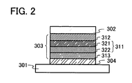
- the light emitting element illustrated in FIG 2 has a structure in which a second electrode 304 serving as a cathode, an EL layer 303, and a first electrode 302 serving as an anode are sequentially stacked over a substrate 301.
- the EL layer 303 includes a hole transporting layer 312, a light emitting layer 311, and an electron transporting layer 313, and the light emitting layer 311 includes a first layer 321 and a second layer 322.
- the first layer 321 is provided closer to the side of the first electrode serving as an anode than the second layer 322.
- the light emitting element is formed over a substrate made of glass, plastic, or the like.
- a plurality of such light emitting elements is formed over one substrate, thereby forming a passive matrix light emitting device.
- a thin film transistor (TFT) may be formed over a substrate of glass, plastic, or the like and a light emitting element may be manufactured over an electrode that is electrically connected to the TFT.
- TFT thin film transistor
- an active matrix light emitting device in which the TFT controls the drive of the light emitting element can be manufactured.
- there is no particular limitation on the structure of the TFT there is no particular limitation on the structure of the TFT.
- a staggered TFT or an inversely staggered TFT may be employed.
- a driver circuit formed over a TFT substrate may be formed using N-channel and P-channel TFTs, or using either N-channel or P-channel TFTs.
- crystallinity of a semiconductor film used for the TFT there is no particular limitation on crystallinity of a semiconductor film used for the TFT. An amorphous semiconductor film may be used, or a crystalline semiconductor film may be used.
- a light emitting region is formed in the vicinity of the center of the light emitting layer, without being formed at the interface between the light emitting layer and the hole transporting layer or at the interface between the light emitting layer and the electron transporting layer.
- the light emitting layer of the light emitting element in the present invention is formed using a compound which is stable even when an oxidative reaction and a reductive reaction are repeated, and thus, the light emitting layer does not deteriorate very much even when light emission by recombination of electrons and holes is repeated. Accordingly, a light emitting element having a long lifetime can be obtained.
- Embodiment Mode 2 will describe a mode of a light emitting element in which a plurality of light emitting units in accordance with the present invention are stacked (hereinafter, also referred to as a stacked type element) with reference to FIG 3 .
- This light emitting element is a light emitting element including a plurality of light emitting units between a first electrode and a second electrode.
- a first light emitting unit 511 and a second light emitting unit 512 are stacked between a first electrode 501 and a second electrode 502. Similar electrodes to those shown in Embodiment Mode 1 can be applied to the first electrode 501 and the second electrode 502.
- the first light emitting unit 511 and the second light emitting unit 512 may have the same structure or different structures to each other, and as the structures, a similar structure to that shown in Embodiment Mode 1 can be employed. That is to say that the light emitting unit includes at least the first layer 121 and the second layer 122. Additionally, the light emitting unit may also include a hole transporting layer, an electron transporting layer, and the like.
- a charge generation layer 513 includes a composite material of an organic compound and a metal oxide.
- the composite material of an organic compound and a metal oxide is the composite material shown in Embodiment Mode 1, and includes an organic compound and a metal oxide such as vanadium oxide, molybdenum oxide, or tungsten oxide.
- the organic compound various compounds such as an aromatic amine compound, a carbazole derivative, aromatic hydrocarbon, and a high molecular compound (oligomer, dendrimer, polymer, or the like) can be used.
- As the organic compound it is preferable to use an organic compound which has a hole transporting property and has a hole mobility of 10 -6 cm 2 /Vs or higher.
- the composite material of the organic compound and the metal oxide can achieve low-voltage driving and low-current driving because of the superior carrier injecting property and carrier transporting property.
- the charge generation layer 513 may be formed by combination of a composite material of the organic compound and the metal oxide with another material.
- a layer containing a composite material of the organic compound and the metal oxide may be combined with a layer containing a compound of a substance selected from electron donating substances and a compound with a high electron transporting property.
- a layer containing a composite material of the organic compound and the metal oxide may be combined with a transparent conductive film.
- the charge generation layer 513 interposed between the first light emitting unit 511 and the second light emitting unit 512 injects electrons to one of these light emitting units and holes to the other thereof when voltage is applied to the first electrode 501 and the second electrode 502.
- this embodiment mode describes the light emitting element having two light emitting units
- the present invention can be similarly applied to a light emitting element in which three or more light emitting units are stacked.
- the charge generation layer is provided between the pair of electrodes so as to partition the plural light emitting units like the light emitting element of this embodiment mode, the element can have a long lifetime with a high luminance while keeping a low current density.
- the light emitting element is applied for illumination, voltage drop due to resistance of an electrode material can be reduced, thereby achieving homogeneous light emission of a large area.
- a light emitting device of low power consumption which can be driven at a low voltage, can be achieved.
- the light emitting units emit light having different colors from each other, light emission of a desired color can be obtained as a whole light emitting element.
- the emission colors of the first light emitting unit and the second light emitting unit are made complementary, so that the light emitting element which emits white light as a whole element can be obtained.
- the word "complementary" means relationship of colors in which an achromatic color is obtained when the colors are mixed. In other words, when lights obtained from substances which emit complementary colors are mixed, white emission can be obtained.
- the same can be applied to a light emitting element having three light emitting units. For example, when the first light emitting unit emits red light, the second light emitting unit emits green light, and the third light emitting unit emits blue light, white light can be obtained as a whole light emitting element.
- Embodiment Mode 3 will describe a light emitting device having a light emitting element of the present invention.
- FIG. 4A is a top view illustrating a light emitting device while FIG 4B is a cross-sectional view taken along lines A-A' and B-B' of FIG. 4A .
- Reference numeral 601 denotes a driver circuit portion (source side driver circuit); 602, a pixel portion; and 603, a driver circuit portion (gate side driver circuit), which are shown with dotted lines.
- reference numeral 604 denotes a sealing substrate; 605, a sealing material; and 607, a space surrounded by the sealing material 605.
- a leading wire 608 is a wire to transmit a signal to be input to the source side driver circuit 601 and the gate side driver circuit 603, and receive a video signal, a clock signal, a start signal, a reset signal, and the like from an FPC (flexible printed circuit) 609, which serves as an external input terminal.
- FPC flexible printed circuit
- this FPC may be provided with a printed wiring board (PWB).
- PWB printed wiring board
- the driver circuit portion and the pixel portion are formed over an element substrate 610.
- the source side driver circuit 601 which is the driver circuit portion, and one pixel in the pixel portion 602 are shown.
- CMOS circuit in which an n-channel TFT 623 and a p-channel TFT 624 are combined is formed.
- a driver circuit may be formed by using various circuits such as a CMOS circuit, a PMOS circuit, and an NMOS circuit.
- this embodiment mode illustrates a driver-integrated type where the driver circuit is formed over the substrate, the present invention is not limited to this, and the driver circuit may be formed outside the substrate, not over the substrate.
- the pixel portion 602 is formed by a plurality of pixels each including a switching TFT 611, a current control TFT 612, and a first electrode 613 electrically connected to a drain of the current control TFT 612.
- An insulator 614 is formed so as to cover an end portion of the first electrode 613.
- the insulator 614 is formed by using a positive photosensitive acrylic resin film.
- an upper end portion or a lower end portion of the insulator 614 is formed so as to have a curved surface with a curvature.
- a curved surface with a curvature 0.2 to 3 ⁇ m.
- the insulator 614 either a negative type which becomes insoluble in etchant by irradiation with light or a positive type which becomes soluble in etchant by irradiation with light can be used.
- the first electrode 613 can be formed with various metals, alloys, electrically conductive compounds, or mixtures thereof. If the first electrode is used as an anode, it is preferable to use, among those materials, a metal, alloy, electrically conductive compound, or mixture thereof having a high work function (work function of 4.0 eV or higher), or the like. For example, a single layer of indium oxide-tin oxide containing silicon, indium oxide-zinc oxide, a titanium nitride film, a chromium film, a tungsten film, a Zn film, a Pt film, or the like can be used.
- a multilayer including a titanium nitride film and a film containing aluminum as its main component; a three-layer structure including a titanium nitride film, a film containing aluminum as its main component, and a titanium nitride film; or the like can be used.
- the multilayer structure achieves to have low wiring resistance, favorable ohmic contact, and a function as an anode.
- the EL layer 616 is formed by various methods such as an evaporation method using an evaporation mask, an inkjet method, a spin coating method, and the like.
- the EL layer 616 includes the light emitting layer described in Embodiment Mode 1 or Embodiment Mode 2.
- a low molecular material, oligomer, dendrimer, or a high molecular material may be used.
- the material for the EL layer not only an organic compound but also an inorganic compound may be used.
- the material for the second electrode 617 various metals, alloys, electrically conductive compounds, mixtures of these, or the like can be used. If the second electrode is used as a cathode, it is preferable to use, among them, a metal, alloy, electrically conductive compound, mixture of these, or the like having a low work function (work function of 3.8 eV or lower).
- a metal, alloy, electrically conductive compound, mixture of these, or the like having a low work function (work function of 3.8 eV or lower).
- an element belonging to Group 1 or Group 2 in the periodic table i.e., an alkali metal such as lithium (Li) or cesium (Cs), an alkaline earth metal such as magnesium (Mg), calcium (Ca), or strontium (Sr), an alloy containing any of these (such as MgAg or AILi), or the like can be given.
- the second electrode 617 is preferably formed by using a multilayer of a metal thin film whose thickness is made thin, and a transparent conductive film (indium oxide-tin oxide (ITO), indium oxide-tin oxide including silicon or silicon oxide, indium oxide-zinc oxide (IZO), indium oxide containing tungsten oxide and zinc oxide (IWZO), or the like).
- ITO indium oxide-tin oxide
- IZO indium oxide-tin oxide including silicon or silicon oxide
- IWZO indium oxide containing tungsten oxide and zinc oxide
- the sealing substrate 604 and the element substrate 610 are attached to each other by the sealing material 605, the light emitting element 618 is provided in the space 607 surrounded by the element substrate 610, the sealing substrate 604, and the sealing material 605.
- the space 607 is filled with filler, and may be filled with an inert gas (such as nitrogen or argon), the sealing material 605, or the like.
- An epoxy-based resin is preferable for the sealing material 605.
- the material preferably allows as little moisture and oxygen as possible to penetrate.
- a plastic substrate made of FRP (fiberglass-reinforced plastics), PVF (polyvinyl fluoride), polyester, acrylic, or the like can be used besides a glass substrate or a quartz substrate.
- the light emitting device having the light emitting element of the present invention can be obtained.
- the light emitting device of the present invention includes the light emitting element described in Embodiment Mode 1 or Embodiment Mode 2. Thus, the light emitting device can have a long lifetime.
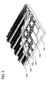
- FIG. 5 is a perspective view of a passive matrix type light emitting device manufactured by applying the present invention.
- an EL layer 955 is provided between an electrode 952 and an electrode 956 over a substrate 951.
- An end portion of the electrode 952 is covered with an insulating layer 953.
- a partition layer 954 is provided over the insulating layer 953. Side walls of the partition layer 954 have such a gradient that the distance becomes shorter between one side wall and the other side wall as they approach the substrate surface.
- a cross section of the partition layer 954 in a short-side direction is trapezoid-like, in which a bottom side (a side in a similar direction to a surface direction of the insulating layer 953, which is in contact with the insulating layer 953) is shorter than an upper side (a side in a similar direction to the surface direction of the insulating layer 953, which is not in contact with the insulating layer 953).
- a bottom side a side in a similar direction to a surface direction of the insulating layer 953, which is in contact with the insulating layer 953
- an upper side a side in a similar direction to the surface direction of the insulating layer 953, which is not in contact with the insulating layer 953).
- Embodiment Mode 4 will describe electronic devices of the present invention, which include the light emitting device described in Embodiment Mode 3 as a part thereof.
- the electronic devices of the present invention each have the light emitting element described in Embodiment Mode 1 or Embodiment Mode 2, and a display portion having a long lifetime.
- cameras such as video cameras or digital cameras, goggle-type displays, navigation systems, audio reproducing devices (such as car audio components or audio components), computers, game machines, mobile information terminals (mobile computers, cellular phones, mobile game machines, or electronic books), image reproducing devices equipped with a recording medium (specifically, devices equipped with a display device for reproducing a recording medium such as digital versatile disk (DVD) and displaying the image), and the like are given.
- audio reproducing devices such as car audio components or audio components
- computers game machines
- mobile information terminals mobile computers, cellular phones, mobile game machines, or electronic books
- image reproducing devices equipped with a recording medium specifically, devices equipped with a display device for reproducing a recording medium such as digital versatile disk (DVD) and displaying the image
- DVD digital versatile disk
- FIG. 6A shows a television device according to the present invention, which includes a housing 9101, a support 9102, a display portion 9103, a speaker portion 9104, a video input terminal 9105, and the like.
- the display portion 9103 is formed by arranging similar light emitting elements to those described in Embodiment Modes 1 and 2 in a matrix form.
- the light emitting elements have an advantage of long lifetime. Since the display portion 9103 formed using the light emitting elements also has the similar advantage, this television device has a long lifetime. In other words, the television device which can endure long use can be provided.
- FIG 6B shows a computer according to the present invention, which includes a main body 9201, a housing 9202, a display portion 9203, a keyboard 9204, an external connection port 9205, a pointing device 9206, and the like.
- the display portion 9203 is formed by arranging similar light emitting elements to those described in Embodiment Modes 1 and 2 in a matrix form.
- the light emitting elements have an advantage of long lifetime. Since the display portion 9203 formed using the light emitting elements also has the similar advantage, this computer has a long lifetime. In other words, the computer which can endure long use can be provided.
- FIG. 6C shows a cellular phone according to the present invention, which includes a main body 9401, a housing 9402, a display portion 9403, an audio input portion 9404, an audio output portion 9405, an operation keys 9406, an external connection port 9407, an antenna 9408, and the like.
- the display portion 9403 is formed by arranging similar light emitting elements to those described in Embodiment Modes 1 and 2 in a matrix form.
- the light emitting elements have an advantage of long lifetime. Since the display portion 9403 formed using the light emitting elements also has the similar advantage, this cellular phone has a long lifetime. In other words, the cellular phone which can endure long use can be provided.
- FIG 6D shows a camera according to the present invention, which includes a main body 9501, a display portion 9502, a housing 9503, an external connection port 9504, a remote control receiving portion 9505, an image receiving portion 9506, a battery 9507, an audio input portion 9508, an operation key 9509, an eyepiece portion 9510, and the like.
- the display portion 9502 is formed by arranging similar light emitting elements to those described in Embodiment Modes 1 and 2 in a matrix form.
- the light emitting elements have an advantage of long lifetime. Since the display portion 9502 formed using the light emitting elements also has the similar advantage, this camera has a long lifetime. In other words, the camera which can endure long use can be provided.
- application range of the light emitting device of the present invention is quite wide, and this light emitting device can be applied to electronic devices of every field.
- an electronic device having a display portion with a long lifetime which can endure long use can be provided.
- the light emitting device of the present invention can be used as an illumination device.
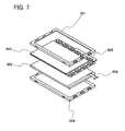
- An example of using the light emitting element of the present invention as an illumination device will be described with reference to FIG 7 .
- FIG. 7 shows an example of a liquid crystal display device in which the light emitting device of the present invention is used as a backlight.
- the liquid crystal display device shown in FIG. 7 includes a housing 901, a liquid crystal layer 902, a backlight 903, and a housing 904, in which the liquid crystal layer 902 is connected to a driver IC 905.
- the backlight 903 uses the light emitting device of the present invention, and current is supplied to the backlight 903 through a terminal 906.
- the backlight of the liquid crystal display device When the light emitting device of the present invention is used as the backlight of the liquid crystal display device, the backlight having a long lifetime can be obtained. Moreover, since the light emitting device of the present invention is an illumination device of surface light emission and the enlargement of the light emitting device is possible, the backlight can be made larger and the liquid crystal display device can also have a larger area. Moreover, since the light emitting device of the present invention is thin and consumes less electric power, reduction in thickness and power consumption of the display device is possible.
- FIG. 8 illustrates an example in which the light emitting device of the present invention is used as a desk lamp, which is an illumination device.
- the desk lamp illustrated in FIG. 8 includes a housing 2001 and a light source 2002.
- the light emitting device of the present invention is used as the light source 2002. Since the light emitting device of the present invention has a long lifetime, the desk lamp can also have a long lifetime.
- FIG 9 illustrates an example of using the light emitting device of the present invention as an interior illumination device 3001. Since the light emitting device of the present invention can be enlarged, the light emitting device can be used as a large-area illumination device. Moreover, since the light emitting device of the present invention has a long lifetime, the illumination device can also have a long lifetime. Thus, a television device 3002 of the present invention as shown in FIG. 6A can be installed in the room where the light emitting device of the present invention is used as the interior illumination device 3001, so that pubic broadcasting and movies can be watched. In such a case, since both of the television device and the illumination device have long lifetimes, frequency of replacement of the illumination device and the television device can be reduced, and environmental load can be reduced.
- Example 1 will specifically describe a light emitting element of the present invention with reference to FIG. 11 .
- Structural formulas of organic compounds used in this example are shown below. Note that a structural formula of a high molecular compound is omitted.
- a film of indium oxide-tin oxide containing silicon oxide was formed over a glass substrate 2100 by a sputtering method to form a first electrode 2101.
- the thickness of the first electrode 2101 was 110 nm and the electrode area was 2 mm x 2 mm.
- a hole injecting layer 2102 was formed over the first electrode 2101.
- the rotation condition was as follows: rotation was conducted at 300 rpm (3 seconds), and then at 2000 rpm (20 seconds). Then, the solution A was dropped and rotation was conducted at 300 rpm (3 seconds), then at 2000 rpm (60 seconds), and further at 3000 rpm (10 seconds).
- uneven application of the solution A is suppressed and uniformity of a PEDOT/PSS layer can be improved. Thereafter, drying by heating under reduced pressure was performed for 1 hour in a vacuum oven where the temperature was set at 110 °C.
- a light emitting layer 2103 was formed over the hole injecting layer 2102.
- a layer containing Super Yellow and rubrene was formed as a first light emitting layer 2121.
- 0.1 g of Super Yellow Catalog No.: PDY132, Merck Ltd.
- the preparation of the solution was performed under an environment where the O 2 concentration and the H 2 O concentration are low. This solution was dropped and applied by a spin coating method.
- the rotation condition was as follows: rotation was conducted at 300 rpm (3 seconds), then at 1000 rpm (60 seconds), and further at 2500 rpm (10 seconds). Thereafter, drying at normal pressure was performed at 80 °C in a nitrogen atmosphere for 10 minutes, and then drying by heating under reduced pressure was performed in a vacuum oven for 20 minutes.
- the thickness of the first light emitting layer 2121 obtained was 80 nm.
- a second light emitting layer 2122 was formed over the first light emitting layer 2121 by a vacuum evaporation method using resistance heating.
- the substrate was fixed to a substrate holder provided in a vacuum evaporation apparatus so that a surface on which the first light emitting layer 2121 was formed faces downward.
- the pressure was reduced to approximately 10 -4 Pa, and co-evaporation of tris(8-quinolinolato)aluminum (abbr.: Alq) and rubrene was performed on the first light emitting layer 2121 to form the second light emitting layer 2122.
- a co-evaporation method is an evaporation method in which evaporation is performed from a plurality of evaporation sources at the same time in one treatment chamber.
- a film of bathophenanthroline (abbr.: BPhen) was formed over the light emitting layer 2103 to have a thickness of 20 nm by an evaporation method using resistance heating, thereby forming an electron transporting layer 2104.
- a film of lithium fluoride (LiF) was formed over the electron transporting layer 2104 to have a thickness of 1 nm by an evaporation method using resistance heating, thereby forming an electron injecting layer 2105.
- a film of aluminum was formed to have a thickness of 200 nm by an evaporation method using resistance heating, thereby forming a second electrode 2106.
- the light emitting element 1 was formed.
- a layer of Alq was formed with a thickness of 10 nm, and a comparative light emitting element 2 was formed. Other layers were formed similar to the light emitting element 1.
- a comparative light emitting element 3 which was an element having a structure where the second light emitting layer 2122 and the electron transporting layer 2104 in the light emitting element 1 were not provided, was formed. That is, a layer of LiF that was an electron injecting layer was formed over a layer containing Super Yellow and rubrene. Other layers were formed similar to the light emitting element 1.
- the light emitting element 1, the comparative light emitting element 2, and the comparative light emitting element 3 obtained in the above-described manner were put in a glove box containing a nitrogen atmosphere and sealing treatment was conducted so that the light emitting elements are not exposed to air. Then, operation characteristics of these light emitting elements were measured. The measurement was conducted at room temperature (atmosphere kept at 25 °C).
- FIG. 12 Light emission spectra of the light emitting element 1, the comparative light emitting element 2, and the comparative light emitting element 3 are shown in FIG. 12 .
- the light emission spectra shown in FIG. 12 were obtained when a current of 1 mA flowed through each of the light emitting elements.
- each of the light emitting element 1, the comparative light emitting element 2, and the comparative light emitting element 3 exhibits light emission from rubrene.
- FIG. 13 shows results of a continuous lighting test in which the light emitting element 1, the comparative light emitting element 2, and the comparative light emitting element 3 were continuously lit by constant current driving with the initial luminance set at 1000 cd/m 2 .
- the vertical axis indicates the normalized luminance when 1000 cd/m 2 is assumed as 100 %.
- FIG. 13 shows the test results for 0.5 hours from the start of testing. From FIG. 13 , it is found that initial deterioration of the light emitting element 1 is suppressed considerably compared to those of the comparative light emitting element 2 and the comparative light emitting element 3. Furthermore, the luminance of the light emitting element 1 after 50 hours from the start of testing keeps 73 % of the initial luminance, whereas that of the comparative light emitting element 2 decreases to 70 % of the initial luminance and that of the comparative light emitting element 3 decreases to 43 % of the initial luminance.
Landscapes
- Physics & Mathematics (AREA)
- Optics & Photonics (AREA)
- Chemical & Material Sciences (AREA)
- Engineering & Computer Science (AREA)
- Materials Engineering (AREA)
- Organic Chemistry (AREA)
- Electroluminescent Light Sources (AREA)
Applications Claiming Priority (1)
| Application Number | Priority Date | Filing Date | Title |
|---|---|---|---|
| JP2006327666 | 2006-12-04 |
Publications (3)
| Publication Number | Publication Date |
|---|---|
| EP1930969A2 true EP1930969A2 (de) | 2008-06-11 |
| EP1930969A3 EP1930969A3 (de) | 2013-11-20 |
| EP1930969B1 EP1930969B1 (de) | 2019-07-10 |
Family
ID=39135254
Family Applications (1)
| Application Number | Title | Priority Date | Filing Date |
|---|---|---|---|
| EP07023467.9A Not-in-force EP1930969B1 (de) | 2006-12-04 | 2007-12-04 | Lichtemittierende Vorrichtung |
Country Status (4)
| Country | Link |
|---|---|
| US (1) | US9397308B2 (de) |
| EP (1) | EP1930969B1 (de) |
| JP (1) | JP2008166746A (de) |
| KR (1) | KR101452201B1 (de) |
Families Citing this family (17)
| Publication number | Priority date | Publication date | Assignee | Title |
|---|---|---|---|---|
| CN101253150B (zh) * | 2005-09-02 | 2012-06-06 | 株式会社半导体能源研究所 | 蒽衍生物 |
| KR101084100B1 (ko) | 2006-06-01 | 2011-11-16 | 가부시키가이샤 한도오따이 에네루기 켄큐쇼 | 발광소자 |
| EP2066629B1 (de) * | 2006-09-28 | 2017-05-17 | Semiconductor Energy Laboratory Co, Ltd. | Anthrazenderivat und lichtemittierendes element, lichtemittierende vorrichtung und elektronische vorrichtung mit dem anthrazenderivat |
| WO2008069153A1 (en) * | 2006-12-04 | 2008-06-12 | Semiconductor Energy Laboratory Co., Ltd. | Light-emitting element, light-emitting device, and electronic device |
| WO2009116547A1 (en) * | 2008-03-18 | 2009-09-24 | Semiconductor Energy Laboratory Co., Ltd. | Light-emitting element, light-emitting device and electronic device |
| CN101978784B (zh) * | 2008-03-18 | 2012-12-05 | 株式会社半导体能源研究所 | 发光元件、发光装置及电子装置 |
| DE102008039361B4 (de) * | 2008-05-30 | 2025-02-06 | Pictiva Displays International Limited | Elektronische Vorrichtung |
| CN101752514B (zh) * | 2008-12-17 | 2015-11-25 | 株式会社半导体能源研究所 | 发光元件、照明装置、发光装置以及电子设备 |
| TWI583253B (zh) * | 2009-01-21 | 2017-05-11 | 半導體能源研究所股份有限公司 | 發光元件,發光裝置以及電子裝置 |
| JP5841406B2 (ja) | 2010-11-05 | 2016-01-13 | 株式会社半導体エネルギー研究所 | 照明装置 |
| JP5948052B2 (ja) | 2010-12-28 | 2016-07-06 | 株式会社半導体エネルギー研究所 | 照明装置 |
| KR102015568B1 (ko) | 2012-08-27 | 2019-08-28 | 삼성전자주식회사 | 반도체 소자의 제조 방법 |
| WO2015064491A1 (ja) * | 2013-10-28 | 2015-05-07 | シャープ株式会社 | 有機エレクトロルミネッセンスパネル |
| CN108475699B (zh) | 2015-12-28 | 2021-11-16 | 株式会社半导体能源研究所 | 半导体装置、包括该半导体装置的显示装置 |
| US10096658B2 (en) * | 2016-04-22 | 2018-10-09 | Semiconductor Energy Laboratory Co., Ltd. | Light-emitting element, display device, electronic device, and lighting device |
| JP6895794B2 (ja) | 2016-04-27 | 2021-06-30 | 株式会社半導体エネルギー研究所 | 表示装置、表示モジュールおよび電子機器 |
| US10475869B2 (en) | 2016-08-23 | 2019-11-12 | Semiconductor Energy Laboratory Co., Ltd. | Display device including display element and transistor |
Citations (2)
| Publication number | Priority date | Publication date | Assignee | Title |
|---|---|---|---|---|
| JPH06158038A (ja) | 1992-11-17 | 1994-06-07 | Pioneer Electron Corp | 有機エレクトロルミネッセンス素子 |
| JP2006327666A (ja) | 2005-05-30 | 2006-12-07 | Toyo Seikan Kaisha Ltd | 容器用把手・把手付容器及びその製造方法 |
Family Cites Families (150)
| Publication number | Priority date | Publication date | Assignee | Title |
|---|---|---|---|---|
| TW542851B (en) * | 1996-05-15 | 2003-07-21 | Chemipro Kasei Kaisha Ltd | Multicolor organic electroluminescence element, its manufacturing method, and a display using the same |
| JP3949214B2 (ja) * | 1997-03-18 | 2007-07-25 | 出光興産株式会社 | 有機エレクトロルミネッセンス素子 |
| US5972247A (en) | 1998-03-20 | 1999-10-26 | Eastman Kodak Company | Organic electroluminescent elements for stable blue electroluminescent devices |
| JP2000231987A (ja) | 1999-02-10 | 2000-08-22 | Fujitsu Ltd | 有機エレクトロルミネッセンス素子及びそれを使用した表示装置 |
| JP2000252072A (ja) | 1999-03-03 | 2000-09-14 | Honda Motor Co Ltd | 有機エレクトロルミネッセンス素子とその製造方法 |
| US6521360B2 (en) * | 1999-06-08 | 2003-02-18 | City University Of Hong Kong | White and colored organic electroluminescent devices using single emitting material by novel color change technique |
| JP3589960B2 (ja) * | 1999-09-16 | 2004-11-17 | 株式会社デンソー | 有機el素子 |
| JP2001131174A (ja) * | 1999-11-02 | 2001-05-15 | Sony Corp | バソフェナントロリン化合物及びその製造方法 |
| US20010043043A1 (en) | 2000-01-07 | 2001-11-22 | Megumi Aoyama | Organic electroluminescent display panel and organic electroluminescent device used therefor |
| JP4382961B2 (ja) | 2000-05-02 | 2009-12-16 | 富士フイルム株式会社 | 発光素子 |
| JP2001326079A (ja) | 2000-05-17 | 2001-11-22 | Toyota Central Res & Dev Lab Inc | 有機電界発光素子 |
| JP3969941B2 (ja) * | 2000-09-01 | 2007-09-05 | 三洋電機株式会社 | 有機発光素子 |
| US7221088B2 (en) * | 2000-11-29 | 2007-05-22 | The United States Of America As Represented By The Secretary Of The Navy | Universal host for RG or RGB emission in organic light emitting devices |
| SG2009086778A (en) * | 2000-12-28 | 2016-11-29 | Semiconductor Energy Lab Co Ltd | Luminescent device |
| TW545080B (en) | 2000-12-28 | 2003-08-01 | Semiconductor Energy Lab | Light emitting device and method of manufacturing the same |
| US6720090B2 (en) * | 2001-01-02 | 2004-04-13 | Eastman Kodak Company | Organic light emitting diode devices with improved luminance efficiency |
| TW518909B (en) * | 2001-01-17 | 2003-01-21 | Semiconductor Energy Lab | Luminescent device and method of manufacturing same |
| TW519770B (en) * | 2001-01-18 | 2003-02-01 | Semiconductor Energy Lab | Light emitting device and manufacturing method thereof |
| US20020139303A1 (en) | 2001-02-01 | 2002-10-03 | Shunpei Yamazaki | Deposition apparatus and deposition method |
| SG118110A1 (en) * | 2001-02-01 | 2006-01-27 | Semiconductor Energy Lab | Organic light emitting element and display device using the element |
| US20030010288A1 (en) * | 2001-02-08 | 2003-01-16 | Shunpei Yamazaki | Film formation apparatus and film formation method |
| TW582121B (en) * | 2001-02-08 | 2004-04-01 | Semiconductor Energy Lab | Light emitting device |
| US7432116B2 (en) | 2001-02-21 | 2008-10-07 | Semiconductor Energy Laboratory Co., Ltd. | Method and apparatus for film deposition |
| SG118118A1 (en) * | 2001-02-22 | 2006-01-27 | Semiconductor Energy Lab | Organic light emitting device and display using the same |
| WO2002071813A1 (en) * | 2001-03-02 | 2002-09-12 | The Trustees Of Princeton University | Double doped-layer, phosphorescent organic light emitting devices |
| US6680570B2 (en) * | 2001-03-21 | 2004-01-20 | Agilent Technologies, Inc. | Polymer organic light emitting device with improved color control |
| JP2002289360A (ja) * | 2001-03-27 | 2002-10-04 | Univ Toyama | 有機電界発光素子 |
| DE60236859D1 (de) * | 2001-04-19 | 2010-08-12 | Tdk Corp | Verbindung geeignet für den einsatz in organischen elektrolumineszenselementen und organische elektrolumineszenselemente |
| US6998487B2 (en) * | 2001-04-27 | 2006-02-14 | Lg Chem, Ltd. | Double-spiro organic compounds and organic electroluminescent devices using the same |
| JP4220253B2 (ja) | 2001-05-18 | 2009-02-04 | ケンブリッジ・ユニバーシティ・テクニカル・サービシズ・リミテッド | エレクトロルミネセンス装置 |
| US7199515B2 (en) * | 2001-06-01 | 2007-04-03 | Semiconductor Energy Laboratory Co., Ltd. | Organic light emitting element and light emitting device using the element |
| US6699597B2 (en) * | 2001-08-16 | 2004-03-02 | 3M Innovative Properties Company | Method and materials for patterning of an amorphous, non-polymeric, organic matrix with electrically active material disposed therein |
| US6603150B2 (en) * | 2001-09-28 | 2003-08-05 | Eastman Kodak Company | Organic light-emitting diode having an interface layer between the hole-transporting layer and the light-emitting layer |
| US6956240B2 (en) | 2001-10-30 | 2005-10-18 | Semiconductor Energy Laboratory Co., Ltd. | Light emitting device |
| JP3815685B2 (ja) * | 2001-11-22 | 2006-08-30 | キヤノン株式会社 | 発光素子及びその製造方法及び発光装置 |
| US7141817B2 (en) * | 2001-11-30 | 2006-11-28 | Semiconductor Energy Laboratory Co., Ltd. | Light emitting device |
| US6723445B2 (en) * | 2001-12-31 | 2004-04-20 | Canon Kabushiki Kaisha | Organic light-emitting devices |
| US6872472B2 (en) | 2002-02-15 | 2005-03-29 | Eastman Kodak Company | Providing an organic electroluminescent device having stacked electroluminescent units |
| KR20020025918A (ko) * | 2002-02-15 | 2002-04-04 | 박병주 | 습식 공정으로 제작된 유기 반도체 디바이스 및 유기전계발광 소자 |
| WO2003078542A1 (en) * | 2002-03-19 | 2003-09-25 | Neoview Co., Ltd. | Red organic light-emitting compound and organic light-emitting device comprising the same |
| JP3933591B2 (ja) | 2002-03-26 | 2007-06-20 | 淳二 城戸 | 有機エレクトロルミネッセント素子 |
| JP4226835B2 (ja) * | 2002-03-29 | 2009-02-18 | 三星エスディアイ株式会社 | 発光素子、その製造方法およびこれを用いた表示装置 |
| JP4060113B2 (ja) * | 2002-04-05 | 2008-03-12 | 株式会社半導体エネルギー研究所 | 発光装置 |
| DE10224021B4 (de) | 2002-05-24 | 2006-06-01 | Novaled Gmbh | Phosphoreszentes lichtemittierendes Bauelement mit organischen Schichten |
| KR20030093016A (ko) * | 2002-06-01 | 2003-12-06 | 삼성에스디아이 주식회사 | 유기 전계발광 소자 |
| US20040097725A1 (en) | 2002-07-10 | 2004-05-20 | Norman Herron | Charge transport compositions and electronic devices made with such compositions |
| US7169482B2 (en) * | 2002-07-26 | 2007-01-30 | Lg.Philips Lcd Co., Ltd. | Display device with anthracene and triazine derivatives |
| US20040018380A1 (en) * | 2002-07-26 | 2004-01-29 | Xerox Corporation | Display device with anthracene and triazine derivatives |
| TWI272874B (en) * | 2002-08-09 | 2007-02-01 | Semiconductor Energy Lab | Organic electroluminescent device |
| JP4368638B2 (ja) | 2002-08-09 | 2009-11-18 | 株式会社半導体エネルギー研究所 | 有機エレクトロルミネッセント素子 |
| US20060017040A9 (en) | 2002-08-09 | 2006-01-26 | Takao Suzuki | Novel triarylamine polymer, process for producing the same, and use thereof |
| US6905787B2 (en) * | 2002-08-22 | 2005-06-14 | Fuji Photo Film Co., Ltd. | Light emitting element |
| JP4272954B2 (ja) | 2002-08-22 | 2009-06-03 | 富士フイルム株式会社 | 発光素子 |
| US6982179B2 (en) * | 2002-11-15 | 2006-01-03 | University Display Corporation | Structure and method of fabricating organic devices |
| US20040132228A1 (en) * | 2002-12-17 | 2004-07-08 | Honeywell International Inc. | Method and system for fabricating an OLED |
| AU2003301015A1 (en) | 2002-12-17 | 2004-07-22 | Honeywell International, Inc. | Method and system for fabricating an oled |
| US20040126617A1 (en) | 2002-12-31 | 2004-07-01 | Eastman Kodak Company | Efficient electroluminescent device |
| US20040219390A1 (en) | 2003-01-23 | 2004-11-04 | Honeywell International, Inc. | Benzoxazinone and quinazolinone derivatives |
| JP4032180B2 (ja) | 2003-02-06 | 2008-01-16 | 東ソー株式会社 | 新規トリアリールアミンポリマー、その製造方法及びその用途 |
| KR20040072004A (ko) | 2003-02-07 | 2004-08-16 | 삼성에스디아이 주식회사 | 유기 전계 발광 소자용 발광 화합물 및 그를 이용한 유기전계발광 소자 |
| TWI265750B (en) | 2003-02-27 | 2006-11-01 | Toyota Jidoshokki Kk | Organic electro-luminescence devices |
| US6991859B2 (en) * | 2003-03-18 | 2006-01-31 | Eastman Kodak Company | Cascaded organic electroluminescent devices |
| US7862906B2 (en) * | 2003-04-09 | 2011-01-04 | Semiconductor Energy Laboratory Co., Ltd. | Electroluminescent element and light-emitting device |
| WO2004097954A1 (en) * | 2003-04-28 | 2004-11-11 | Zheng-Hong Lu | Light-emitting devices with fullerene layer |
| JP2004335122A (ja) | 2003-04-30 | 2004-11-25 | Takasago Internatl Corp | 発光素子 |
| JP4487587B2 (ja) * | 2003-05-27 | 2010-06-23 | 株式会社デンソー | 有機el素子およびその製造方法 |
| JP3984190B2 (ja) | 2003-05-30 | 2007-10-03 | Tdk株式会社 | 有機el素子 |
| JP2005011734A (ja) | 2003-06-20 | 2005-01-13 | Sony Corp | 表示素子および表示装置 |
| JP4479171B2 (ja) | 2003-06-20 | 2010-06-09 | ソニー株式会社 | 表示素子 |
| WO2005006816A1 (ja) * | 2003-07-11 | 2005-01-20 | Idemitsu Kosan Co., Ltd. | 白色系有機エレクトロルミネッセンス素子 |
| WO2005010012A1 (ja) * | 2003-07-28 | 2005-02-03 | Semiconductor Energy Laboratory Co., Ltd. | 発光性有機化合物およびそれを用いた発光素子 |
| KR100994083B1 (ko) | 2003-07-31 | 2010-11-12 | 미쓰비시 가가꾸 가부시키가이샤 | 화합물, 전하 수송 재료 및 유기 전계 발광 소자 |
| US7511421B2 (en) | 2003-08-25 | 2009-03-31 | Semiconductor Energy Laboratory Co., Ltd. | Mixed metal and organic electrode for organic device |
| KR100552964B1 (ko) * | 2003-08-28 | 2006-02-15 | 삼성에스디아이 주식회사 | 평판표시소자용 도너필름 및 그를 이용한유기전계발광소자의 제조방법 |
| US20050052119A1 (en) * | 2003-09-08 | 2005-03-10 | Gang Yu | Organic electronic device having low background luminescence |
| JP2005107890A (ja) | 2003-09-30 | 2005-04-21 | Sanyo Electric Co Ltd | El表示装置 |
| JP3728309B2 (ja) | 2003-09-30 | 2005-12-21 | 三洋電機株式会社 | 有機エレクトロルミネッセント素子及び有機エレクトロルミネッセント素子用有機化合物 |
| EP1521316B1 (de) * | 2003-10-03 | 2016-05-25 | Semiconductor Energy Laboratory Co., Ltd. | Verfahren zur herstellung ein lichtemittierendes Element |
| JP4547599B2 (ja) | 2003-10-15 | 2010-09-22 | 奇美電子股▲ふん▼有限公司 | 画像表示装置 |
| US7205716B2 (en) * | 2003-10-20 | 2007-04-17 | Semiconductor Energy Laboratory Co., Ltd. | Light-emitting device |
| TWI220101B (en) * | 2003-10-30 | 2004-08-01 | Au Optronics Corp | Organic electroluminescence device and fabricating method thereof |
| US7061011B2 (en) * | 2003-11-26 | 2006-06-13 | The Trustees Of Princeton University | Bipolar organic devices |
| US7935433B2 (en) * | 2003-12-25 | 2011-05-03 | Fujifilm Corporation | Organic EL element, organic EL display apparatus, method for manufacturing organic EL element, and apparatus for manufacturing organic EL element |
| US20050147844A1 (en) * | 2004-01-05 | 2005-07-07 | Eastman Kodak Company | White oled devices with color filter arrays |
| US7368178B2 (en) * | 2004-01-08 | 2008-05-06 | Eastman Kodak Company | Stable organic light-emitting devices using aminoanthracenes |
| JP4378186B2 (ja) * | 2004-02-06 | 2009-12-02 | キヤノン株式会社 | 有機el素子アレイ |
| TW200541401A (en) | 2004-02-13 | 2005-12-16 | Idemitsu Kosan Co | Organic electroluminescent device |
| JP2005235403A (ja) * | 2004-02-17 | 2005-09-02 | Hitachi Displays Ltd | 有機・el表示装置 |
| JP5167571B2 (ja) * | 2004-02-18 | 2013-03-21 | ソニー株式会社 | 表示素子 |
| JP4393249B2 (ja) | 2004-03-31 | 2010-01-06 | 株式会社 日立ディスプレイズ | 有機発光素子,画像表示装置、及びその製造方法 |
| KR101110890B1 (ko) | 2004-04-02 | 2012-03-13 | 이데미쓰 고산 가부시키가이샤 | 전자 장벽층을 개재시킨 2개의 발광층을 갖는 유기전기발광 소자 |
| US7192659B2 (en) * | 2004-04-14 | 2007-03-20 | Eastman Kodak Company | OLED device using reduced drive voltage |
| JP4384536B2 (ja) | 2004-04-27 | 2009-12-16 | 三井化学株式会社 | アントラセン化合物、および該アントラセン化合物を含有する有機電界発光素子 |
| KR100690348B1 (ko) | 2004-05-11 | 2007-03-09 | 주식회사 엘지화학 | 유기 전기 소자 |
| US7811677B2 (en) | 2004-05-20 | 2010-10-12 | Semiconductor Energy Laboratory Co., Ltd. | Light emitting element and light emitting device |
| CN1965613B (zh) * | 2004-05-21 | 2010-06-16 | 株式会社半导体能源研究所 | 发光元件及使用该元件的发光装置 |
| US7622200B2 (en) | 2004-05-21 | 2009-11-24 | Semiconductor Energy Laboratory Co., Ltd. | Light emitting element |
| US20060006792A1 (en) * | 2004-07-09 | 2006-01-12 | Eastman Kodak Company | Flat panel light emitting devices with two sided |
| KR100669717B1 (ko) * | 2004-07-29 | 2007-01-16 | 삼성에스디아이 주식회사 | 유기 전계 발광 소자 |
| JP2006049057A (ja) | 2004-08-04 | 2006-02-16 | Hitachi Displays Ltd | 有機el表示装置 |
| EP1624502B1 (de) * | 2004-08-04 | 2015-11-18 | Semiconductor Energy Laboratory Co., Ltd. | Lichtemittierende Vorrichtung, Anzeigevorrichtung und elektronisches Gerät |
| US7300731B2 (en) * | 2004-08-10 | 2007-11-27 | E.I. Du Pont De Nemours And Company | Spatially-doped charge transport layers |
| US20060036114A1 (en) * | 2004-08-13 | 2006-02-16 | Suning Wang | Organoboron luminescent compounds and methods of making and using same |
| US20060040131A1 (en) * | 2004-08-19 | 2006-02-23 | Eastman Kodak Company | OLEDs with improved operational lifetime |
| US7273663B2 (en) * | 2004-08-20 | 2007-09-25 | Eastman Kodak Company | White OLED having multiple white electroluminescence units |
| EP1825532B1 (de) | 2004-08-27 | 2013-04-24 | Showa Denko K.K. | Organisches elektrolumineszenzbauelement und herstellungsverfahren dafür |
| KR100719991B1 (ko) * | 2004-09-30 | 2007-05-21 | 산요덴키가부시키가이샤 | 일렉트로루미네센스 소자 |
| KR101205192B1 (ko) * | 2004-10-01 | 2012-11-27 | 가부시키가이샤 한도오따이 에네루기 켄큐쇼 | 발광 소자 및 발광 장치 |
| JP4830122B2 (ja) | 2004-10-21 | 2011-12-07 | コニカミノルタホールディングス株式会社 | 有機エレクトロルミネッセンス素子、照明装置および表示装置 |
| US20060088730A1 (en) * | 2004-10-25 | 2006-04-27 | Eastman Kodak Company | Organic light-emitting devices with improved performance |
| US20060091794A1 (en) * | 2004-11-04 | 2006-05-04 | Eastman Kodak Company | Passive matrix OLED display having increased size |
| KR100787423B1 (ko) * | 2004-11-05 | 2007-12-26 | 삼성에스디아이 주식회사 | 유기 전계 발광 소자 |
| WO2006059665A1 (en) * | 2004-11-30 | 2006-06-08 | Semiconductor Energy Laboratory Co., Ltd. | Light emitting element and electronic device using the same |
| WO2006062177A1 (en) | 2004-12-06 | 2006-06-15 | Semiconductor Energy Laboratory Co., Ltd. | Composite material including organic compound and inorganic compound, light-emitting element and light-emitting device using the composite compound, and manufacturing method of the light-emitting element |
| KR101249378B1 (ko) * | 2004-12-28 | 2013-04-01 | 가부시키가이샤 한도오따이 에네루기 켄큐쇼 | 발광 소자 |
| CN101124202B (zh) | 2004-12-28 | 2012-05-23 | 株式会社半导体能源研究所 | 蒽衍生物、发光元件、发光器件和使用它们的电子设备 |
| JP4548121B2 (ja) | 2005-01-14 | 2010-09-22 | セイコーエプソン株式会社 | 発光素子の製造方法 |
| JP4939809B2 (ja) | 2005-01-21 | 2012-05-30 | 株式会社半導体エネルギー研究所 | 発光装置 |
| US7494722B2 (en) * | 2005-02-23 | 2009-02-24 | Eastman Kodak Company | Tandem OLED having an organic intermediate connector |
| DE502005002342D1 (de) * | 2005-03-15 | 2008-02-07 | Novaled Ag | Lichtemittierendes Bauelement |
| US7649197B2 (en) * | 2005-03-23 | 2010-01-19 | Semiconductor Energy Laboratory Co., Ltd. | Composite material, and light emitting element and light emitting device using the composite material |
| TWI307250B (en) | 2005-03-23 | 2009-03-01 | Au Optronics Corp | Organic electroluminescent device |
| CN101184732B (zh) | 2005-03-28 | 2012-05-16 | 株式会社半导体能源研究所 | 蒽衍生物、发光元件用材料、发光元件、发光装置和电子器件 |
| US7745019B2 (en) | 2005-04-28 | 2010-06-29 | Semiconductor Energy Laboratory Co., Ltd. | Light emitting element and light emitting device and method of manufacturing light emitting element |
| JP4915544B2 (ja) | 2005-05-11 | 2012-04-11 | パナソニック株式会社 | 有機エレクトロルミネッセンス素子 |
| US7564182B2 (en) * | 2005-06-29 | 2009-07-21 | Eastman Kodak Company | Broadband light tandem OLED display |
| US7531959B2 (en) * | 2005-06-29 | 2009-05-12 | Eastman Kodak Company | White light tandem OLED display with filters |
| KR101324758B1 (ko) | 2005-07-14 | 2013-11-06 | 가부시키가이샤 한도오따이 에네루기 켄큐쇼 | 카르바졸 유도체, 및 그것을 사용하여 얻어진 발광소자용재료, 발광소자, 전자기기 |
| KR100806812B1 (ko) * | 2005-07-25 | 2008-02-25 | 엘지.필립스 엘시디 주식회사 | 유기 el 소자 및 그 제조방법 |
| KR100672535B1 (ko) * | 2005-07-25 | 2007-01-24 | 엘지전자 주식회사 | 유기 el 소자 및 그 제조방법 |
| US7879464B2 (en) | 2005-07-27 | 2011-02-01 | Semiconductor Energy Laboratory Co., Ltd. | Anthracene derivative, material for light emitting element, light emitting element, light emitting device, and electronic appliance |
| US20070048545A1 (en) * | 2005-08-31 | 2007-03-01 | Eastman Kodak Company | Electron-transporting layer for white OLED device |
| US20070046189A1 (en) * | 2005-08-31 | 2007-03-01 | Eastman Kodak Company | Intermediate connector for a tandem OLED device |
| CN101253150B (zh) | 2005-09-02 | 2012-06-06 | 株式会社半导体能源研究所 | 蒽衍生物 |
| US20070077349A1 (en) * | 2005-09-30 | 2007-04-05 | Eastman Kodak Company | Patterning OLED device electrodes and optical material |
| US8148891B2 (en) * | 2005-10-04 | 2012-04-03 | Universal Display Corporation | Electron impeding layer for high efficiency phosphorescent OLEDs |
| EP1777758A1 (de) | 2005-10-18 | 2007-04-25 | Semiconductor Energy Laboratory Co., Ltd. | Organische lichtemittierende Vorrichtung |
| US7645524B2 (en) * | 2005-10-19 | 2010-01-12 | Eastman Kodak Company | OLED device with improved high temperature operation |
| US7767317B2 (en) | 2005-10-26 | 2010-08-03 | Global Oled Technology Llc | Organic element for low voltage electroluminescent devices |
| TWI371987B (en) * | 2006-01-18 | 2012-09-01 | Lg Chemical Ltd | Oled having stacked organic light-emitting units |
| US20070247061A1 (en) | 2006-04-20 | 2007-10-25 | Vadim Adamovich | Multiple dopant emissive layer OLEDs |
| US7733009B2 (en) * | 2006-04-27 | 2010-06-08 | Global Oled Technology Llc | Electroluminescent device including an anthracene derivative |
| US20070252517A1 (en) | 2006-04-27 | 2007-11-01 | Eastman Kodak Company | Electroluminescent device including an anthracene derivative |
| US7582508B2 (en) | 2006-05-31 | 2009-09-01 | Byoung-Choo Park | Method for manufacturing an organic semiconductor device that utilizes ionic salt |
| KR101084100B1 (ko) | 2006-06-01 | 2011-11-16 | 가부시키가이샤 한도오따이 에네루기 켄큐쇼 | 발광소자 |
| EP1863105B1 (de) * | 2006-06-02 | 2020-02-19 | Semiconductor Energy Laboratory Co., Ltd. | Lichtemittierendes Element, lichtemittierende Vorrichtung und elektronische Vorrichtung |
| US7902742B2 (en) * | 2006-07-04 | 2011-03-08 | Semiconductor Energy Laboratory Co., Ltd. | Light-emitting element, light-emitting device, and electronic device |
| WO2008069153A1 (en) * | 2006-12-04 | 2008-06-12 | Semiconductor Energy Laboratory Co., Ltd. | Light-emitting element, light-emitting device, and electronic device |
| EP1973386B8 (de) | 2007-03-23 | 2016-01-13 | Semiconductor Energy Laboratory Co., Ltd. | Lichtemittierende vorrichtung und elektronische vorrichtung |
| US7759854B2 (en) | 2007-05-30 | 2010-07-20 | Global Oled Technology Llc | Lamp with adjustable color |
-
2007
- 2007-11-28 US US11/946,484 patent/US9397308B2/en not_active Expired - Fee Related
- 2007-12-04 JP JP2007313030A patent/JP2008166746A/ja not_active Withdrawn
- 2007-12-04 KR KR1020070124963A patent/KR101452201B1/ko not_active Expired - Fee Related
- 2007-12-04 EP EP07023467.9A patent/EP1930969B1/de not_active Not-in-force
Patent Citations (2)
| Publication number | Priority date | Publication date | Assignee | Title |
|---|---|---|---|---|
| JPH06158038A (ja) | 1992-11-17 | 1994-06-07 | Pioneer Electron Corp | 有機エレクトロルミネッセンス素子 |
| JP2006327666A (ja) | 2005-05-30 | 2006-12-07 | Toyo Seikan Kaisha Ltd | 容器用把手・把手付容器及びその製造方法 |
Also Published As
| Publication number | Publication date |
|---|---|
| EP1930969A3 (de) | 2013-11-20 |
| KR101452201B1 (ko) | 2014-10-21 |
| US9397308B2 (en) | 2016-07-19 |
| JP2008166746A (ja) | 2008-07-17 |
| EP1930969B1 (de) | 2019-07-10 |
| US20080261075A1 (en) | 2008-10-23 |
| KR20080051095A (ko) | 2008-06-10 |
Similar Documents
| Publication | Publication Date | Title |
|---|---|---|
| EP1930969B1 (de) | Lichtemittierende Vorrichtung | |
| JP7397135B2 (ja) | 発光素子、発光装置および電子機器 | |
| CN102255054B (zh) | 发光元件、发光装置和电子装置 | |
| CN102117892B (zh) | 发光元件、发光装置和电子装置 | |
| TWI474758B (zh) | 發光元件、發光裝置、和電子裝置 | |
| US8916857B2 (en) | Light-emitting element, light-emitting device, and electronic device | |
| JP5564526B2 (ja) | 発光素子、発光装置、照明装置および電子機器 |
Legal Events
| Date | Code | Title | Description |
|---|---|---|---|
| PUAI | Public reference made under article 153(3) epc to a published international application that has entered the european phase |
Free format text: ORIGINAL CODE: 0009012 |
|
| AK | Designated contracting states |
Kind code of ref document: A2 Designated state(s): AT BE BG CH CY CZ DE DK EE ES FI FR GB GR HU IE IS IT LI LT LU LV MC MT NL PL PT RO SE SI SK TR |
|
| AX | Request for extension of the european patent |
Extension state: AL BA HR MK RS |
|
| RIC1 | Information provided on ipc code assigned before grant |
Ipc: H01L 51/50 20060101ALI20130403BHEP Ipc: H01L 51/54 20060101AFI20130403BHEP |
|
| PUAL | Search report despatched |
Free format text: ORIGINAL CODE: 0009013 |
|
| AK | Designated contracting states |
Kind code of ref document: A3 Designated state(s): AT BE BG CH CY CZ DE DK EE ES FI FR GB GR HU IE IS IT LI LT LU LV MC MT NL PL PT RO SE SI SK TR |
|
| AX | Request for extension of the european patent |
Extension state: AL BA HR MK RS |
|
| RIC1 | Information provided on ipc code assigned before grant |
Ipc: H01L 51/54 20060101AFI20131015BHEP Ipc: H01L 51/50 20060101ALI20131015BHEP |
|
| 17P | Request for examination filed |
Effective date: 20140520 |
|
| RBV | Designated contracting states (corrected) |
Designated state(s): AT BE BG CH CY CZ DE DK EE ES FI FR GB GR HU IE IS IT LI LT LU LV MC MT NL PL PT RO SE SI SK TR |
|
| AKX | Designation fees paid |
Designated state(s): DE FI FR GB NL |
|
| 17Q | First examination report despatched |
Effective date: 20180710 |
|
| GRAP | Despatch of communication of intention to grant a patent |
Free format text: ORIGINAL CODE: EPIDOSNIGR1 |
|
| INTG | Intention to grant announced |
Effective date: 20190128 |
|
| GRAS | Grant fee paid |
Free format text: ORIGINAL CODE: EPIDOSNIGR3 |
|
| GRAA | (expected) grant |
Free format text: ORIGINAL CODE: 0009210 |
|
| AK | Designated contracting states |
Kind code of ref document: B1 Designated state(s): DE FI FR GB NL |
|
| REG | Reference to a national code |
Ref country code: GB Ref legal event code: FG4D |
|
| REG | Reference to a national code |
Ref country code: DE Ref legal event code: R096 Ref document number: 602007058781 Country of ref document: DE |
|
| REG | Reference to a national code |
Ref country code: NL Ref legal event code: MP Effective date: 20190710 |
|
| PG25 | Lapsed in a contracting state [announced via postgrant information from national office to epo] |
Ref country code: NL Free format text: LAPSE BECAUSE OF FAILURE TO SUBMIT A TRANSLATION OF THE DESCRIPTION OR TO PAY THE FEE WITHIN THE PRESCRIBED TIME-LIMIT Effective date: 20190710 Ref country code: FI Free format text: LAPSE BECAUSE OF FAILURE TO SUBMIT A TRANSLATION OF THE DESCRIPTION OR TO PAY THE FEE WITHIN THE PRESCRIBED TIME-LIMIT Effective date: 20190710 |
|
| REG | Reference to a national code |
Ref country code: DE Ref legal event code: R097 Ref document number: 602007058781 Country of ref document: DE |
|
| PLBE | No opposition filed within time limit |
Free format text: ORIGINAL CODE: 0009261 |
|
| STAA | Information on the status of an ep patent application or granted ep patent |
Free format text: STATUS: NO OPPOSITION FILED WITHIN TIME LIMIT |
|
| 26N | No opposition filed |
Effective date: 20200603 |
|
| GBPC | Gb: european patent ceased through non-payment of renewal fee |
Effective date: 20191204 |
|
| PG25 | Lapsed in a contracting state [announced via postgrant information from national office to epo] |
Ref country code: FR Free format text: LAPSE BECAUSE OF NON-PAYMENT OF DUE FEES Effective date: 20191231 Ref country code: GB Free format text: LAPSE BECAUSE OF NON-PAYMENT OF DUE FEES Effective date: 20191204 |
|
| PGFP | Annual fee paid to national office [announced via postgrant information from national office to epo] |
Ref country code: DE Payment date: 20211012 Year of fee payment: 15 |
|
| REG | Reference to a national code |
Ref country code: DE Ref legal event code: R079 Ref document number: 602007058781 Country of ref document: DE Free format text: PREVIOUS MAIN CLASS: H01L0051540000 Ipc: H10K0085000000 |
|
| REG | Reference to a national code |
Ref country code: DE Ref legal event code: R119 Ref document number: 602007058781 Country of ref document: DE |
|
| PG25 | Lapsed in a contracting state [announced via postgrant information from national office to epo] |
Ref country code: DE Free format text: LAPSE BECAUSE OF NON-PAYMENT OF DUE FEES Effective date: 20230701 |