EP1652008B1 - Method for monitoring an immersion lithography system - Google Patents
Method for monitoring an immersion lithography system Download PDFInfo
- Publication number
- EP1652008B1 EP1652008B1 EP04757263A EP04757263A EP1652008B1 EP 1652008 B1 EP1652008 B1 EP 1652008B1 EP 04757263 A EP04757263 A EP 04757263A EP 04757263 A EP04757263 A EP 04757263A EP 1652008 B1 EP1652008 B1 EP 1652008B1
- Authority
- EP
- European Patent Office
- Prior art keywords
- index
- refraction
- immersion medium
- wafer
- immersion
- Prior art date
- Legal status (The legal status is an assumption and is not a legal conclusion. Google has not performed a legal analysis and makes no representation as to the accuracy of the status listed.)
- Expired - Lifetime
Links
Images
Classifications
-
- G—PHYSICS
- G03—PHOTOGRAPHY; CINEMATOGRAPHY; ANALOGOUS TECHNIQUES USING WAVES OTHER THAN OPTICAL WAVES; ELECTROGRAPHY; HOLOGRAPHY
- G03F—PHOTOMECHANICAL PRODUCTION OF TEXTURED OR PATTERNED SURFACES, e.g. FOR PRINTING, FOR PROCESSING OF SEMICONDUCTOR DEVICES; MATERIALS THEREFOR; ORIGINALS THEREFOR; APPARATUS SPECIALLY ADAPTED THEREFOR
- G03F7/00—Photomechanical, e.g. photolithographic, production of textured or patterned surfaces, e.g. printing surfaces; Materials therefor, e.g. comprising photoresists; Apparatus specially adapted therefor
- G03F7/20—Exposure; Apparatus therefor
-
- G—PHYSICS
- G03—PHOTOGRAPHY; CINEMATOGRAPHY; ANALOGOUS TECHNIQUES USING WAVES OTHER THAN OPTICAL WAVES; ELECTROGRAPHY; HOLOGRAPHY
- G03F—PHOTOMECHANICAL PRODUCTION OF TEXTURED OR PATTERNED SURFACES, e.g. FOR PRINTING, FOR PROCESSING OF SEMICONDUCTOR DEVICES; MATERIALS THEREFOR; ORIGINALS THEREFOR; APPARATUS SPECIALLY ADAPTED THEREFOR
- G03F7/00—Photomechanical, e.g. photolithographic, production of textured or patterned surfaces, e.g. printing surfaces; Materials therefor, e.g. comprising photoresists; Apparatus specially adapted therefor
- G03F7/70—Microphotolithographic exposure; Apparatus therefor
- G03F7/70216—Mask projection systems
- G03F7/70341—Details of immersion lithography aspects, e.g. exposure media or control of immersion liquid supply
Definitions
- the present invention relates generally to the field of integrated circuit manufacture and, more particularly, to a method for monitoring an immersion lithography system.
- CMOS complementary metal-oxide-semiconductor
- CMOS complementary metal-oxide-semiconductor
- PR photo resist
- the PR material can become soluble such that it can be removed to selectively expose an underlying layer (e.g., a semiconductor layer, a metal or metal containing layer, a dielectric layer, etc.). Portions of the PR layer not exposed to a threshold amount of light energy will not be removed and serve to protect the underlying layer.
- the exposed portions of the underlying layer can then be etched (e.g., by using a chemical wet etch or a dry reactive ion etch (RIE)) such that the pattern formed from the PR layer is transferred to the underlying layer.
- the PR layer can be used to block dopant implantation into the protected portions of the underlying layer or to retard reaction of the protected portions of the underlying layer. Thereafter, the remaining portions of the PR layer can be stripped.
- immersion lithography the wafer to imaged by a lithography system is placed in a liquid medium, through which the patterned light is transmitted.
- the immersion medium replaces an air gap that is conventionally present between the final lens of a conventional dry lithography imaging system and the wafer.
- the invention is directed to a method of monitoring an immersion lithography system as defined in claim1.
- the method includes immersing a wafer to be exposed in a liquid immersion medium; detecting an index of refraction of the immersion medium in a volume of the immersion medium through which an exposure pattern is configured to traverse; and determining if the index of refraction is acceptable for exposing the wafer with the exposure pattern.
- the disclosure further provides a monitoring and control system for an immersion lithography system.
- the immersion lithography system can include a chamber for receiving a wafer to be exposed and immersing the wafer in an immersion medium and an imaging subsystem for directing an exposure pattern towards the wafer and through the immersion medium.
- the monitoring and control system can include an immersion medium monitoring subsystem including an interferometer assembly for directing a test portion of a laser beam through the immersion medium and for directing a control portion of the laser beam around the chamber, and a detector assembly for receiving the test portion and the control portion, the detector outputting a signal indicative of an index of refraction of the immersion medium in a volume of the immersion medium through which the exposure pattern is configured to traverse; and a controller, the controller receiving the signal indicative of the index of refraction and determining if the index of refraction is acceptable for exposing the wafer with the exposure pattern.
- an immersion medium monitoring subsystem including an interferometer assembly for directing a test portion of a laser beam through the immersion medium and for directing a control portion of the laser beam around the chamber, and a detector assembly for receiving the test portion and the control portion, the detector outputting a signal indicative of an index of refraction of the immersion medium in a volume of the immersion medium through which the exposure pattern is configured to traverse; and a controller, the controller receiving the
- Example ICs include general purpose microprocessors made from thousands or millions of transistors, a flash memory array or any other dedicated circuitry.
- lithography such as micromachines, disk drive heads, gene chips, micro electro-mechanical systems (MEMS) and so forth.
- the apparatus and methods described herein can provide for real-time detection of a key parameter for immersion lithography. Namely, index of refraction of a liquid immersion medium can be monitored to determine if conditions are favorable for exposing a wafer. In addition, the immersion medium can be monitored for the presence of a foreign body (e.g., a particle and/or a bubble).
- a foreign body e.g., a particle and/or a bubble
- the system 10 can be, for example, a step-and-repeat exposure system or a step-and-scan exposure system, but is not limited to these example systems.
- the system 10 can include a light source 14 for directing light energy 16 towards a mask 18 (sometimes referred to as a reticle).
- the light energy 16 can have, for example, a deep ultraviolet wavelength (e.g., about 248 nm or about 193 nm), or a vacuum ultraviolet (VUV) wavelength (e.g., about 157 nm).
- a deep ultraviolet wavelength e.g., about 248 nm or about 193 nm
- VUV vacuum ultraviolet
- the mask 18 selectively blocks light energy 16 such that a light energy pattern 16'defined by the mask 18 is transferred towards the wafer 12.
- the imaging subsystem 20 may include a series of lenses and/or reflectors for use in scaling and directing the energy pattern 16' towards the wafer 12 in the form of an imaging (or exposure) light energy pattern 22.
- the imaging pattern 22 (or exposure pattern) is transmitted by the imaging subsystem 20 through an immersion fluid, or immersion medium 24, that has a relatively high index of refraction (e.g., an index of refraction greater than 1).
- the immersion medium 24 can be a liquid.
- purified de-ionized water can be used in conjunction with a 193 nm light source 14 (e.g., an argon fluorine (ArF) laser).
- ArF argon fluorine
- polyfluoroethers can be used in conjunction with a 157 nm light source 14.
- Changes and variations to the index of refraction (also referred to as refractive index) of the immersion medium 24 can have a significant effect of the imaging pattern 22 incident on the wafer 12. For example, if the index of refraction of the immersion medium 24 uniformly changes across the volume through which the imaging pattern 24 traverses, a focus shift may result and/or spherical aberrations could result. If the index of refraction of the immersion medium 24 varies non-uniformly across the volume through which the imaging pattern 22 traverses, unpredictable aberrations in the imaging pattern 22 incident on the wafer 12 are very likely to occur. As should be apparent, changes and/or variations in the index of refraction of the immersion medium 24 can lead to defects in the integrated circuit being fabricated on the wafer 12.
- the cause(s) of changes and/or variations in the index of refraction of the immersion medium 24 can include, for example, turbulence of the immersion medium 24, changes in density of the immersion medium 24, changes in temperature of the immersion medium 24 and so forth.
- dry lithography i.e., the imaging pattern traverses an air or gas gap
- immersion lithography it is believed that at least some of the energy from the imaging pattern 22 will be absorbed by the immersion medium 24.
- heat may be transferred from the wafer 12 to immersion medium 24.
- the absorption of energy by the immersion medium 24, even in small quantities, may be sufficient to create a variation in the index of refraction of the immersion medium 24 that could adversely effect the imaging pattern 22.
- the wafer 12 may be mounted on a stage (not shown) that is moved relative to the imaging subsystem 20. For example, the wafer 12 may be exposed, then moved about 30 mm to a new location and stopped for a second exposure and so forth. Wafer motion rates can be about 250 mm/second to about 500 mm/second. This movement may create turbulence or other changes to the properties of the immersion medium 24 that could result in variations in the index of refraction of the immersion medium 24.
- the immersion medium 24 may be purposefully placed in motion (e.g., in a flow pattern over the wafer 12) or subjected to hydraulic pressure. These factors may also invoke variations in the index of refraction of the immersion medium 24.
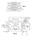
- FIG. 2 shown is a schematic block diagram of an immersion medium 24 monitoring and control assembly 26 for use with the exemplary IC processing arrangement 10.
- the assembly 26 includes a controller 28, such as a computer programmed to control the IC processing arrangement 10 and an immersion medium control subsystem 30.
- the controller 28 can receive an input signal or signals from an immersion medium monitoring subsystem 32.
- the imaging subsystem 20 can include an output lens 34, or other final optical structure. At least a portion of the imaging subsystem 20, including the lens 34, can enter a chamber 36 containing the immersion medium 24 and the wafer 12. The lens 34 will be in intimate contact with the immersion medium 24 such that the imaging pattern 22 output by the lens 34 is projected through the immersion medium 24 and is incident onto at least a portion of the wafer 12, which is disposed or immersed in the immersion medium 24.
- the volume of immersion medium 24 in the field of view of the imaging pattern 22 (e.g., the volume or portion of the immersion medium 24 through which the imaging pattern 22 traverses) will be referred to herein as traversed volume 38.
- the lens 34 can be disposed about 1 mm above the wafer 12.
- the distance between the lens 34 and wafer 12 may vary depending on the illumination wavelength, the immersion medium 24, the specific processing arrangement 10, the devices being fabricated on the wafer 12, the particular photo resist employed, an so forth.
- the traversal volume can be about 25 mm wide and 10 mm long, although these parameters can vary widely.
- the monitoring subsystem 32 includes devices to monitor the index of refraction of the immersion medium 24 or a portion thereof, such as the index of refraction throughout the traversal volume 38 portion of the immersion medium 24.
- the monitoring subsystem 32 can include at least one interferometer assembly, such as a Michelson interferometer. Therefore, the monitoring subsystem 32 can include, for example, a laser beam source 40, a pair of beam splitters 42a and 42b, a pair of mirrors 44a and 44b and a detector assembly 46.
- the detector assembly 46 can be implemented with, for example, a photomultiplier tube. In one embodiment, the beam generated by the laser 40 is several hundred microns in diameter.
- multiple beams produced by one or more lasers 40 can be used to simultaneously monitor the index of refraction of the immersion medium 24 along several lines in the traversal volume 38. If needed, multiple beam splitters 42, mirrors 44 and detectors can be added. For simplicity, the monitoring associated with only one beam is shown and described. However, implementing a multiple beam interferometer system should be apparent to one of ordinary skill in the art. In an alternative embodiment, one or more beams can be scanned through the traversal volume 38 to generate an indication of the index of refraction of the immersion medium 24 throughout the traversal volume 38.
- the laser 40 should be selected to generate an output wavelength to avoid activation of the photo resist disposed on the wafer 12.
- the wavelength should be about 300 nm or above (e.g., in the visible spectrum), but this parameter can vary depending on the properties of the photo resist used.
- a helium neon (HeNe) laser can be used. This laser beam can optionally be subjected to Zeeman splitting by an axial magnetic field.
- the chamber 36 can include an entrance window 46a through which a test portion 48a of the beam generated by the laser 40 enters the chamber 36 and an exit window 46b through which the test portion 48a exits the chamber 36.
- the windows 46 should be transmissive of the wavelength of the beam generated by the laser 40 and can include an anti-reflective coating or other mechanism for facilitating test portion 48a transmission.
- the beam output by the laser 40 is split into the test portion 48a and a control portion 48b by the beam splitter 42a.
- the control portion 48b can travel through an air medium around the chamber 36 as guided by the mirrors 44a and 44b.
- the test portion 48a and the control portion 48b are brought together by the beam splitter 42b such that the test portion 48a and the control portion 48b are directed to the detector assembly 46.
- the detector assembly 46 can be configured to determine the phase difference between the test portion 48a and the control portion 48b.
- the phase difference can be used as a direct indicator of the index of refraction of the immersion medium 24 at the wavelength of the beam generated by the laser 40.
- test portion 48a may be a first wavelength generated by Zeeman splitting and a second wavelength generated by the Zeeman splitting can be used for the control portion 48b.
- conventional heterodyne detection can be used to determine a frequency difference between the test and control portions. The frequency difference is then indicative of refractive index of the immersion medium 24.
- multiple beams can be used to determine the index of refraction of the immersion medium 24 at multiple locations of the traversal volume 38, if not all of the traversal volume 38.
- one or more beams can be scanned across the traversal volume 38 to determine the index of refraction at multiple locations of the traversal volume 38, if not all of the traversal volume 38.
- the measurement or measurements of index of refraction, or raw data from the monitoring subsystem 32 from which the measurement(s) of index of refraction can be calculated, can be transmitted from the detector assembly 46 to the controller 28 in the form of an input signal or signals.
- the controller 28 can process the input signal(s) to determine if the index of refraction of the immersion medium 24 is uniform across the traversal volume and/or the controller 28 can process the input signal(s) to determine if the index of refraction of the immersion medium 24 is within an acceptable range for imaging the wafer 12 with the system 10.
- determination of index of refraction acceptability can include calculating changes or variations in the immersion medium's 24 refractive index at the exposure wavelength (e.g., ultraviolet, DUV or VUV) by correlation to the results derived from the monitoring subsystem 32, which operates a different wavelength (e.g., in the visible spectrum).
- Refractive index changes of a chemically pure, or nearly pure, medium are based in large part to changes in density of the medium.
- density is indirectly measured and this measurement can be used to infer or derive the refractive index at a different wavelength (e.g., the wavelength of the exposure light source 14).
- the controller 28 can issue commands to the system 10 to expose the wafer 12. However, if the index of refraction is not uniform across the traversal volume 38 or if the index of refraction is not within an acceptable range for exposing the wafer 12 at the exposure wavelength, then it can be concluded that conditions are not favorable for exposing the wafer 12 and the controller 28 be programmed to defer exposing the wafer.
- the controller 28 can be programmed to carry out one or more specified actions. For example, the controller 28 can be programmed to simply wait for a predetermined period of time during which it is expected that the immersion medium 24 may settle to a more favorable state. After the predetermined period, the index of refraction of the immersion medium 24 can be retested. In another example, the controller 28 be programmed to take a corrective action. Example correction actions can include sending commands to the immersion medium control subsystem 30, such as commands to cool or warm the immersion medium 24, to decrease or increase an immersion medium 24 flow rate, and so forth. In another example, the controller 28 can be programmed to alert an operator to the unfavorable environment for imaging the wafer 12.
- Alerting an operator may be reserved for situations where repeated measurements of the immersion medium 24 have revealed unfavorable conditions and/or when the index of refraction of the immersion medium 24 is above a predetermined high threshold or below a predetermined low threshold.
- the controller 28 can be programmed to perform more than one of the foregoing functions, such as waiting a predetermined period of time and taking a corrective action.
- the monitoring subsystem 32 can be used to detect a foreign body 50 in the immersion medium 24.
- the monitoring subsystem 32 is configured to detect the presence of the foreign body 50 in the traversal volume 38.
- the foreign body 50 can include a particle (e.g., an item suspended in the immersion medium 24, such as dust, a contaminant, a stray piece of photo resist, etc.) or a bubble (e.g., an air or other gas pocket in the immersion medium 24).
- the presence of a foreign body 50 in the immersion medium even if very small (e.g., about 50 nm or smaller), can be detrimental to the quality of the pattern imaged on the wafer 12 by the system 10.
- test portion 48a of the beam is incident upon the foreign body 50, some of the test portion 48a may become scattered as scattered light 52.
- the scattered light 52 can be detected by the detector apparatus 46 or by a separate detector assembly.
- laser beams and detectors separate from those used to monitor immersion medium 24 refractive index can be used for monitoring for foreign bodies.
- the detector assembly 46 can transmit a corresponding signal to the controller 48 that, in turn, can defer imaging of the wafer 12.
- the controller 28 can be programmed to carry out one or more specified actions. For example, the controller 28 can be programmed to simply wait for a predetermined period of time during which it is expected that the foreign body will move out of the traversal volume 38. After the predetermined period, the index of refraction of the immersion medium 24 can be retested. In another example, the controller 28 be programmed to take a corrective action.
- Example correction actions can include sending commands to the immersion medium control subsystem 30, such as commands to decrease or increase an immersion medium 24 flow rate.
- the controller 28 can be programmed to alert an operator to the unfavorable environment for imaging the wafer 12. Alerting an operator may be reserved for situations where repeated measurements of the immersion medium 24 have revealed the presence of a foreign body 50.
- the controller 28 can be programmed to perform more than one of the foregoing functions, such as waiting a predetermined period of time and taking a corrective action.
- the controller 28 can also be programmed to factor the refractive index value(s) with other information provided by additional sensors (not shown). Such other information can include thermal sensors that monitor the temperature of the immersion medium 24 and/or imaging subsystem 20 components, sensors that detect the position of the wafer 12, flow rate sensors that monitor the flow or turbulence of the immersion medium 24, and so forth. Based upon a plurality of factors, the controller 28 can be programmed to take one or more of the actions discussed above, or other actions not specifically identified herein.
Landscapes
- Physics & Mathematics (AREA)
- General Physics & Mathematics (AREA)
- Exposure Of Semiconductors, Excluding Electron Or Ion Beam Exposure (AREA)
- Exposure And Positioning Against Photoresist Photosensitive Materials (AREA)
Applications Claiming Priority (2)
| Application Number | Priority Date | Filing Date | Title |
|---|---|---|---|
| US10/628,021 US7006209B2 (en) | 2003-07-25 | 2003-07-25 | Method and apparatus for monitoring and controlling imaging in immersion lithography systems |
| PCT/US2004/023876 WO2005013008A2 (en) | 2003-07-25 | 2004-07-23 | Method for monitoring and controlling imaging in immersion lithography systems |
Publications (2)
| Publication Number | Publication Date |
|---|---|
| EP1652008A2 EP1652008A2 (en) | 2006-05-03 |
| EP1652008B1 true EP1652008B1 (en) | 2011-06-08 |
Family
ID=34080711
Family Applications (1)
| Application Number | Title | Priority Date | Filing Date |
|---|---|---|---|
| EP04757263A Expired - Lifetime EP1652008B1 (en) | 2003-07-25 | 2004-07-23 | Method for monitoring an immersion lithography system |
Country Status (7)
| Country | Link |
|---|---|
| US (1) | US7006209B2 (enExample) |
| EP (1) | EP1652008B1 (enExample) |
| JP (1) | JP4465356B2 (enExample) |
| KR (1) | KR101071966B1 (enExample) |
| CN (1) | CN100538523C (enExample) |
| TW (1) | TWI372947B (enExample) |
| WO (1) | WO2005013008A2 (enExample) |
Families Citing this family (118)
| Publication number | Priority date | Publication date | Assignee | Title |
|---|---|---|---|---|
| KR100588124B1 (ko) | 2002-11-12 | 2006-06-09 | 에이에스엠엘 네델란즈 비.브이. | 리소그래피장치 및 디바이스제조방법 |
| US9482966B2 (en) | 2002-11-12 | 2016-11-01 | Asml Netherlands B.V. | Lithographic apparatus and device manufacturing method |
| US10503084B2 (en) | 2002-11-12 | 2019-12-10 | Asml Netherlands B.V. | Lithographic apparatus and device manufacturing method |
| SG121818A1 (en) | 2002-11-12 | 2006-05-26 | Asml Netherlands Bv | Lithographic apparatus and device manufacturing method |
| US7372541B2 (en) | 2002-11-12 | 2008-05-13 | Asml Netherlands B.V. | Lithographic apparatus and device manufacturing method |
| KR101036114B1 (ko) | 2002-12-10 | 2011-05-23 | 가부시키가이샤 니콘 | 노광장치 및 노광방법, 디바이스 제조방법 |
| SG158745A1 (en) | 2002-12-10 | 2010-02-26 | Nikon Corp | Exposure apparatus and method for producing device |
| US7948604B2 (en) | 2002-12-10 | 2011-05-24 | Nikon Corporation | Exposure apparatus and method for producing device |
| WO2004053952A1 (ja) | 2002-12-10 | 2004-06-24 | Nikon Corporation | 露光装置及びデバイス製造方法 |
| US7242455B2 (en) | 2002-12-10 | 2007-07-10 | Nikon Corporation | Exposure apparatus and method for producing device |
| EP1571697A4 (en) | 2002-12-10 | 2007-07-04 | Nikon Corp | EXPOSURE SYSTEM AND DEVICE PRODUCTION METHOD |
| JP4352874B2 (ja) | 2002-12-10 | 2009-10-28 | 株式会社ニコン | 露光装置及びデバイス製造方法 |
| DE10261775A1 (de) | 2002-12-20 | 2004-07-01 | Carl Zeiss Smt Ag | Vorrichtung zur optischen Vermessung eines Abbildungssystems |
| EP1598855B1 (en) | 2003-02-26 | 2015-04-22 | Nikon Corporation | Exposure apparatus and method, and method of producing apparatus |
| KR101345474B1 (ko) | 2003-03-25 | 2013-12-27 | 가부시키가이샤 니콘 | 노광 장치 및 디바이스 제조 방법 |
| WO2004090956A1 (ja) | 2003-04-07 | 2004-10-21 | Nikon Corporation | 露光装置及びデバイス製造方法 |
| JP4488004B2 (ja) | 2003-04-09 | 2010-06-23 | 株式会社ニコン | 液浸リソグラフィ流体制御システム |
| CN1771463A (zh) | 2003-04-10 | 2006-05-10 | 株式会社尼康 | 用于沉浸光刻装置收集液体的溢出通道 |
| KR101323993B1 (ko) | 2003-04-10 | 2013-10-30 | 가부시키가이샤 니콘 | 액침 리소그래피 장치용 운반 영역을 포함하는 환경 시스템 |
| CN101061429B (zh) | 2003-04-10 | 2015-02-04 | 株式会社尼康 | 包括用于沉浸光刻装置的真空清除的环境系统 |
| EP2161621B1 (en) * | 2003-04-11 | 2018-10-24 | Nikon Corporation | Cleanup method for optics in an immersion lithography apparatus, and corresponding immersion lithography apparatus |
| WO2004092830A2 (en) | 2003-04-11 | 2004-10-28 | Nikon Corporation | Liquid jet and recovery system for immersion lithography |
| SG139733A1 (en) | 2003-04-11 | 2008-02-29 | Nikon Corp | Apparatus having an immersion fluid system configured to maintain immersion fluid in a gap adjacent an optical assembly |
| KR101369582B1 (ko) | 2003-04-17 | 2014-03-04 | 가부시키가이샤 니콘 | 액침 리소그래피에서 이용하기 위한 오토포커스 소자의 광학적 배열 |
| TWI295414B (en) | 2003-05-13 | 2008-04-01 | Asml Netherlands Bv | Lithographic apparatus and device manufacturing method |
| WO2004102646A1 (ja) | 2003-05-15 | 2004-11-25 | Nikon Corporation | 露光装置及びデバイス製造方法 |
| TWI424470B (zh) * | 2003-05-23 | 2014-01-21 | 尼康股份有限公司 | A method of manufacturing an exposure apparatus and an element |
| TWI614794B (zh) | 2003-05-23 | 2018-02-11 | Nikon Corp | 曝光方法及曝光裝置以及元件製造方法 |
| EP2453465A3 (en) | 2003-05-28 | 2018-01-03 | Nikon Corporation | Exposure method, exposure apparatus, and method for producing a device |
| TWI347741B (en) * | 2003-05-30 | 2011-08-21 | Asml Netherlands Bv | Lithographic apparatus and device manufacturing method |
| US7213963B2 (en) | 2003-06-09 | 2007-05-08 | Asml Netherlands B.V. | Lithographic apparatus and device manufacturing method |
| US7317504B2 (en) | 2004-04-08 | 2008-01-08 | Asml Netherlands B.V. | Lithographic apparatus and device manufacturing method |
| EP1486827B1 (en) | 2003-06-11 | 2011-11-02 | ASML Netherlands B.V. | Lithographic apparatus and device manufacturing method |
| KR101520591B1 (ko) | 2003-06-13 | 2015-05-14 | 가부시키가이샤 니콘 | 노광 방법, 기판 스테이지, 노광 장치, 및 디바이스 제조 방법 |
| TWI543235B (zh) | 2003-06-19 | 2016-07-21 | 尼康股份有限公司 | A method of manufacturing an exposure apparatus and an element |
| US6867844B2 (en) | 2003-06-19 | 2005-03-15 | Asml Holding N.V. | Immersion photolithography system and method using microchannel nozzles |
| DE60308161T2 (de) | 2003-06-27 | 2007-08-09 | Asml Netherlands B.V. | Lithographischer Apparat und Verfahren zur Herstellung eines Artikels |
| US6809794B1 (en) * | 2003-06-27 | 2004-10-26 | Asml Holding N.V. | Immersion photolithography system and method using inverted wafer-projection optics interface |
| US7236232B2 (en) | 2003-07-01 | 2007-06-26 | Nikon Corporation | Using isotopically specified fluids as optical elements |
| JP4697138B2 (ja) | 2003-07-08 | 2011-06-08 | 株式会社ニコン | 液浸リソグラフィ装置、液浸リソグラフィ方法、デバイス製造方法 |
| EP2264531B1 (en) | 2003-07-09 | 2013-01-16 | Nikon Corporation | Exposure apparatus and device manufacturing method |
| EP1643543B1 (en) | 2003-07-09 | 2010-11-24 | Nikon Corporation | Exposure apparatus and method for manufacturing device |
| KR101296501B1 (ko) | 2003-07-09 | 2013-08-13 | 가부시키가이샤 니콘 | 노광 장치 및 디바이스 제조 방법 |
| EP1650787A4 (en) | 2003-07-25 | 2007-09-19 | Nikon Corp | INVESTIGATION METHOD AND INVESTIGATION DEVICE FOR AN OPTICAL PROJECTION SYSTEM AND METHOD OF MANUFACTURING AN OPTICAL PROJECTION SYSTEM |
| CN104122760B (zh) | 2003-07-28 | 2017-04-19 | 株式会社尼康 | 曝光装置、器件制造方法 |
| EP1503244A1 (en) | 2003-07-28 | 2005-02-02 | ASML Netherlands B.V. | Lithographic projection apparatus and device manufacturing method |
| US7326522B2 (en) | 2004-02-11 | 2008-02-05 | Asml Netherlands B.V. | Device manufacturing method and a substrate |
| US7175968B2 (en) | 2003-07-28 | 2007-02-13 | Asml Netherlands B.V. | Lithographic apparatus, device manufacturing method and a substrate |
| US7779781B2 (en) | 2003-07-31 | 2010-08-24 | Asml Netherlands B.V. | Lithographic apparatus and device manufacturing method |
| US7061578B2 (en) * | 2003-08-11 | 2006-06-13 | Advanced Micro Devices, Inc. | Method and apparatus for monitoring and controlling imaging in immersion lithography systems |
| US7700267B2 (en) * | 2003-08-11 | 2010-04-20 | Taiwan Semiconductor Manufacturing Company, Ltd. | Immersion fluid for immersion lithography, and method of performing immersion lithography |
| US7579135B2 (en) * | 2003-08-11 | 2009-08-25 | Taiwan Semiconductor Manufacturing Company, Ltd. | Lithography apparatus for manufacture of integrated circuits |
| US6844206B1 (en) * | 2003-08-21 | 2005-01-18 | Advanced Micro Devices, Llp | Refractive index system monitor and control for immersion lithography |
| SG145780A1 (en) | 2003-08-29 | 2008-09-29 | Nikon Corp | Exposure apparatus and device fabricating method |
| TWI263859B (en) | 2003-08-29 | 2006-10-11 | Asml Netherlands Bv | Lithographic apparatus and device manufacturing method |
| KR20170070264A (ko) | 2003-09-03 | 2017-06-21 | 가부시키가이샤 니콘 | 액침 리소그래피용 유체를 제공하기 위한 장치 및 방법 |
| JP4444920B2 (ja) | 2003-09-19 | 2010-03-31 | 株式会社ニコン | 露光装置及びデバイス製造方法 |
| EP1670043B1 (en) | 2003-09-29 | 2013-02-27 | Nikon Corporation | Exposure apparatus, exposure method, and device manufacturing method |
| EP1519231B1 (en) * | 2003-09-29 | 2005-12-21 | ASML Netherlands B.V. | Lithographic apparatus and device manufacturing method |
| JP2005136364A (ja) | 2003-10-08 | 2005-05-26 | Zao Nikon Co Ltd | 基板搬送装置、露光装置、並びにデバイス製造方法 |
| WO2005036623A1 (ja) | 2003-10-08 | 2005-04-21 | Zao Nikon Co., Ltd. | 基板搬送装置及び基板搬送方法、露光装置及び露光方法、デバイス製造方法 |
| KR101111364B1 (ko) | 2003-10-08 | 2012-02-27 | 가부시키가이샤 자오 니콘 | 기판 반송 장치 및 기판 반송 방법, 노광 장치 및 노광방법, 디바이스 제조 방법 |
| TW201738932A (zh) | 2003-10-09 | 2017-11-01 | Nippon Kogaku Kk | 曝光裝置及曝光方法、元件製造方法 |
| EP1524557A1 (en) * | 2003-10-15 | 2005-04-20 | ASML Netherlands B.V. | Lithographic apparatus and device manufacturing method |
| US7411653B2 (en) | 2003-10-28 | 2008-08-12 | Asml Netherlands B.V. | Lithographic apparatus |
| US7352433B2 (en) | 2003-10-28 | 2008-04-01 | Asml Netherlands B.V. | Lithographic apparatus and device manufacturing method |
| JP4295712B2 (ja) | 2003-11-14 | 2009-07-15 | エーエスエムエル ネザーランズ ビー.ブイ. | リソグラフィ装置及び装置製造方法 |
| EP3139214B1 (en) | 2003-12-03 | 2019-01-30 | Nikon Corporation | Exposure apparatus, exposure method, and device manufacturing method |
| DE602004030481D1 (de) | 2003-12-15 | 2011-01-20 | Nippon Kogaku Kk | Bühnensystem, belichtungsvorrichtung und belichtungsverfahren |
| US7394521B2 (en) | 2003-12-23 | 2008-07-01 | Asml Netherlands B.V. | Lithographic apparatus and device manufacturing method |
| EP1706793B1 (en) | 2004-01-20 | 2010-03-03 | Carl Zeiss SMT AG | Exposure apparatus and measuring device for a projection lens |
| US7589822B2 (en) | 2004-02-02 | 2009-09-15 | Nikon Corporation | Stage drive method and stage unit, exposure apparatus, and device manufacturing method |
| WO2005076321A1 (ja) | 2004-02-03 | 2005-08-18 | Nikon Corporation | 露光装置及びデバイス製造方法 |
| US7050146B2 (en) * | 2004-02-09 | 2006-05-23 | Asml Netherlands B.V. | Lithographic apparatus and device manufacturing method |
| US8488102B2 (en) * | 2004-03-18 | 2013-07-16 | Taiwan Semiconductor Manufacturing Company, Ltd. | Immersion fluid for immersion lithography, and method of performing immersion lithography |
| JP4525676B2 (ja) | 2004-03-25 | 2010-08-18 | 株式会社ニコン | 露光装置、露光方法、及びデバイス製造方法 |
| US7898642B2 (en) | 2004-04-14 | 2011-03-01 | Asml Netherlands B.V. | Lithographic apparatus and device manufacturing method |
| US8054448B2 (en) | 2004-05-04 | 2011-11-08 | Nikon Corporation | Apparatus and method for providing fluid for immersion lithography |
| US7616383B2 (en) | 2004-05-18 | 2009-11-10 | Asml Netherlands B.V. | Lithographic apparatus and device manufacturing method |
| WO2005119368A2 (en) | 2004-06-04 | 2005-12-15 | Carl Zeiss Smt Ag | System for measuring the image quality of an optical imaging system |
| WO2005122218A1 (ja) * | 2004-06-09 | 2005-12-22 | Nikon Corporation | 露光装置及びデバイス製造方法 |
| US7463330B2 (en) | 2004-07-07 | 2008-12-09 | Asml Netherlands B.V. | Lithographic apparatus and device manufacturing method |
| KR101342330B1 (ko) | 2004-07-12 | 2013-12-16 | 가부시키가이샤 니콘 | 노광 장치 및 디바이스 제조 방법 |
| JP4983257B2 (ja) | 2004-08-18 | 2012-07-25 | 株式会社ニコン | 露光装置、デバイス製造方法、計測部材、及び計測方法 |
| US7701550B2 (en) | 2004-08-19 | 2010-04-20 | Asml Netherlands B.V. | Lithographic apparatus and device manufacturing method |
| US20060044533A1 (en) * | 2004-08-27 | 2006-03-02 | Asmlholding N.V. | System and method for reducing disturbances caused by movement in an immersion lithography system |
| EP1806773A4 (en) * | 2004-10-13 | 2008-12-31 | Nikon Corp | EXPOSURE DEVICE, EXPOSURE METHOD, AND DEVICE MANUFACTURING METHOD |
| US7158896B1 (en) * | 2004-11-01 | 2007-01-02 | Advanced Micro Devices, Inc. | Real time immersion medium control using scatterometry |
| US8029186B2 (en) * | 2004-11-05 | 2011-10-04 | International Business Machines Corporation | Method for thermal characterization under non-uniform heat load |
| US7289193B1 (en) * | 2004-12-01 | 2007-10-30 | Advanced Micro Devices, Inc. | Frame structure for turbulence control in immersion lithography |
| US8547521B1 (en) * | 2004-12-01 | 2013-10-01 | Advanced Micro Devices, Inc. | Systems and methods that control liquid temperature in immersion lithography to maintain temperature gradient to reduce turbulence |
| US7397533B2 (en) | 2004-12-07 | 2008-07-08 | Asml Netherlands B.V. | Lithographic apparatus and device manufacturing method |
| US7880860B2 (en) | 2004-12-20 | 2011-02-01 | Asml Netherlands B.V. | Lithographic apparatus and device manufacturing method |
| SG124351A1 (en) | 2005-01-14 | 2006-08-30 | Asml Netherlands Bv | Lithographic apparatus and device manufacturing method |
| SG124359A1 (en) | 2005-01-14 | 2006-08-30 | Asml Netherlands Bv | Lithographic apparatus and device manufacturing method |
| US8692973B2 (en) | 2005-01-31 | 2014-04-08 | Nikon Corporation | Exposure apparatus and method for producing device |
| KR20160135859A (ko) | 2005-01-31 | 2016-11-28 | 가부시키가이샤 니콘 | 노광 장치 및 디바이스 제조 방법 |
| US7282701B2 (en) | 2005-02-28 | 2007-10-16 | Asml Netherlands B.V. | Sensor for use in a lithographic apparatus |
| USRE43576E1 (en) | 2005-04-08 | 2012-08-14 | Asml Netherlands B.V. | Dual stage lithographic apparatus and device manufacturing method |
| US20060232753A1 (en) * | 2005-04-19 | 2006-10-19 | Asml Holding N.V. | Liquid immersion lithography system with tilted liquid flow |
| JP2006319064A (ja) * | 2005-05-11 | 2006-11-24 | Canon Inc | 測定装置、露光方法及び装置 |
| FR2890742B1 (fr) * | 2005-09-12 | 2007-11-30 | Production Et De Rech S Appliq | Equipement et procede de surveillance d'un dispositif lithographique a immersion. |
| JP2007103841A (ja) * | 2005-10-07 | 2007-04-19 | Toshiba Corp | 半導体装置の製造方法 |
| US7773195B2 (en) * | 2005-11-29 | 2010-08-10 | Asml Holding N.V. | System and method to increase surface tension and contact angle in immersion lithography |
| US8125610B2 (en) | 2005-12-02 | 2012-02-28 | ASML Metherlands B.V. | Method for preventing or reducing contamination of an immersion type projection apparatus and an immersion type lithographic apparatus |
| US7649611B2 (en) | 2005-12-30 | 2010-01-19 | Asml Netherlands B.V. | Lithographic apparatus and device manufacturing method |
| DE102006021797A1 (de) | 2006-05-09 | 2007-11-15 | Carl Zeiss Smt Ag | Optische Abbildungseinrichtung mit thermischer Dämpfung |
| US20070296937A1 (en) * | 2006-06-26 | 2007-12-27 | International Business Machines Corporation | Illumination light in immersion lithography stepper for particle or bubble detection |
| KR100763334B1 (ko) | 2006-08-03 | 2007-10-04 | 삼성전자주식회사 | 이머젼 매질을 모니터링하는 유니트를 구비하는 이머젼포토리쏘그라피 장비 및 이를 사용하는 이머젼포토리쏘그라피 공정을 모니터링하는 방법 |
| US8045135B2 (en) * | 2006-11-22 | 2011-10-25 | Asml Netherlands B.V. | Lithographic apparatus with a fluid combining unit and related device manufacturing method |
| US7995185B2 (en) | 2006-12-07 | 2011-08-09 | Asml Holding N.V. | Systems and methods for thermally-induced aberration correction in immersion lithography |
| US8237911B2 (en) | 2007-03-15 | 2012-08-07 | Nikon Corporation | Apparatus and methods for keeping immersion fluid adjacent to an optical assembly during wafer exchange in an immersion lithography machine |
| NL1035970A1 (nl) * | 2007-09-28 | 2009-04-03 | Asml Holding Nv | Lithographic Apparatus and Device Manufacturing Method. |
| JP5472101B2 (ja) * | 2008-04-30 | 2014-04-16 | 株式会社ニコン | 露光装置及びデバイス製造方法 |
| US9176393B2 (en) | 2008-05-28 | 2015-11-03 | Asml Netherlands B.V. | Lithographic apparatus and a method of operating the apparatus |
| EP2381310B1 (en) | 2010-04-22 | 2015-05-06 | ASML Netherlands BV | Fluid handling structure and lithographic apparatus |
| CN103885301B (zh) * | 2014-03-21 | 2015-09-16 | 浙江大学 | 浸没式光刻机中浸液传送系统的控制时序的模型匹配方法 |
| US11821838B1 (en) * | 2020-06-01 | 2023-11-21 | Jean-Claude Diels | Spectroscopy in frequency, time, and position with correlated frequency combs |
Family Cites Families (19)
| Publication number | Priority date | Publication date | Assignee | Title |
|---|---|---|---|---|
| US4346164A (en) | 1980-10-06 | 1982-08-24 | Werner Tabarelli | Photolithographic method for the manufacture of integrated circuits |
| JPS57153433A (en) | 1981-03-18 | 1982-09-22 | Hitachi Ltd | Manufacturing device for semiconductor |
| IL66127A (en) | 1982-06-24 | 1987-11-30 | Israel State | Method and apparatus for measuring the index of refraction of fluids |
| US4670637A (en) | 1985-02-11 | 1987-06-02 | The United States Of America As Represented By The Secretary Of The Army | Method and apparatus for transmitting a laser signal through fog |
| US5151752A (en) * | 1988-06-16 | 1992-09-29 | Asahi Kogaku Kogyo K.K. | Method of measuring refractive indices of lens and sample liquid |
| JP2753930B2 (ja) | 1992-11-27 | 1998-05-20 | キヤノン株式会社 | 液浸式投影露光装置 |
| US5422714A (en) | 1993-06-07 | 1995-06-06 | Corning Incorporated | Device for comparing the refractive indices of an optical immersion liquid and a reference glass |
| GB9324926D0 (en) * | 1993-12-04 | 1994-01-26 | Renishaw Plc | Combined interferometer and refractometer |
| JP2982720B2 (ja) * | 1996-04-26 | 1999-11-29 | 日本電気株式会社 | パーティクルモニター装置およびこれを具備した無塵化プロセス装置 |
| US5825043A (en) | 1996-10-07 | 1998-10-20 | Nikon Precision Inc. | Focusing and tilting adjustment system for lithography aligner, manufacturing apparatus or inspection apparatus |
| US6133995A (en) | 1997-05-09 | 2000-10-17 | Sysmex Corporation | Particle measuring apparatus |
| US5900354A (en) | 1997-07-03 | 1999-05-04 | Batchelder; John Samuel | Method for optical inspection and lithography |
| US6241827B1 (en) | 1998-02-17 | 2001-06-05 | Tokyo Electron Limited | Method for cleaning a workpiece |
| JP3833810B2 (ja) | 1998-03-04 | 2006-10-18 | 株式会社日立製作所 | 半導体の製造方法並びにプラズマ処理方法およびその装置 |
| DE10025789A1 (de) | 2000-05-19 | 2001-11-22 | Schmidt & Haensch Gmbh & Co Op | Refraktometer |
| WO2002091078A1 (en) | 2001-05-07 | 2002-11-14 | Massachusetts Institute Of Technology | Methods and apparatus employing an index matching medium |
| EP1489461A1 (en) | 2003-06-11 | 2004-12-22 | ASML Netherlands B.V. | Lithographic apparatus and device manufacturing method |
| EP1486827B1 (en) | 2003-06-11 | 2011-11-02 | ASML Netherlands B.V. | Lithographic apparatus and device manufacturing method |
| US7236232B2 (en) | 2003-07-01 | 2007-06-26 | Nikon Corporation | Using isotopically specified fluids as optical elements |
-
2003
- 2003-07-25 US US10/628,021 patent/US7006209B2/en not_active Expired - Lifetime
-
2004
- 2004-07-23 WO PCT/US2004/023876 patent/WO2005013008A2/en not_active Ceased
- 2004-07-23 TW TW093122007A patent/TWI372947B/zh not_active IP Right Cessation
- 2004-07-23 JP JP2006521952A patent/JP4465356B2/ja not_active Expired - Fee Related
- 2004-07-23 CN CNB2004800195324A patent/CN100538523C/zh not_active Expired - Lifetime
- 2004-07-23 EP EP04757263A patent/EP1652008B1/en not_active Expired - Lifetime
- 2004-07-23 KR KR1020067001296A patent/KR101071966B1/ko not_active Expired - Fee Related
Also Published As
| Publication number | Publication date |
|---|---|
| KR20060058684A (ko) | 2006-05-30 |
| TW200510965A (en) | 2005-03-16 |
| JP4465356B2 (ja) | 2010-05-19 |
| US7006209B2 (en) | 2006-02-28 |
| CN1820229A (zh) | 2006-08-16 |
| EP1652008A2 (en) | 2006-05-03 |
| WO2005013008A3 (en) | 2005-11-10 |
| WO2005013008A2 (en) | 2005-02-10 |
| US20050018208A1 (en) | 2005-01-27 |
| TWI372947B (en) | 2012-09-21 |
| KR101071966B1 (ko) | 2011-10-11 |
| CN100538523C (zh) | 2009-09-09 |
| JP2007500449A (ja) | 2007-01-11 |
Similar Documents
| Publication | Publication Date | Title |
|---|---|---|
| EP1652008B1 (en) | Method for monitoring an immersion lithography system | |
| US7061578B2 (en) | Method and apparatus for monitoring and controlling imaging in immersion lithography systems | |
| JP5208119B2 (ja) | 光センサ装置 | |
| TWI477892B (zh) | 具有傅立葉濾波及影像比較的光罩檢測 | |
| KR102499301B1 (ko) | 방사선 분석 시스템 | |
| US9939730B2 (en) | Optical assembly | |
| TWI485395B (zh) | 時間差光罩檢測 | |
| JP2009088508A (ja) | 液浸リソグラフィに関する方法および液浸リソグラフィ装置 | |
| WO2020126248A1 (en) | Methods and apparatus for metrology | |
| JP6084227B2 (ja) | リソグラフィ装置及び方法 | |
| US8982316B2 (en) | Lithographic apparatus, a metrology apparatus and a method of using the apparatus | |
| US8902403B2 (en) | Lithographic apparatus and device manufacturing method | |
| TW201312299A (zh) | 用於微影裝置之位階感測器配置、微影裝置及器件製造方法 | |
| KR101097193B1 (ko) | 리소그래피 장치 및 습도 측정 시스템 | |
| JP2008078642A (ja) | リソグラフ要素の汚染測定方法およびシステム | |
| CN117157587A (zh) | 光刻设备、温度传感器、和光纤布拉格光栅传感器 | |
| KR20110110263A (ko) | 특성을 결정하는 방법 | |
| CN110832402A (zh) | 清除方法、显露装置、光刻设备和器件制造方法 |
Legal Events
| Date | Code | Title | Description |
|---|---|---|---|
| PUAI | Public reference made under article 153(3) epc to a published international application that has entered the european phase |
Free format text: ORIGINAL CODE: 0009012 |
|
| 17P | Request for examination filed |
Effective date: 20051222 |
|
| AK | Designated contracting states |
Kind code of ref document: A2 Designated state(s): AT BE BG CH CY CZ DE DK EE ES FI FR GB GR HU IE IT LI LU MC NL PL PT RO SE SI SK TR |
|
| AX | Request for extension of the european patent |
Extension state: AL HR LT LV MK |
|
| DAX | Request for extension of the european patent (deleted) | ||
| RBV | Designated contracting states (corrected) |
Designated state(s): DE GB |
|
| RAP1 | Party data changed (applicant data changed or rights of an application transferred) |
Owner name: GLOBALFOUNDRIES, INC. |
|
| GRAP | Despatch of communication of intention to grant a patent |
Free format text: ORIGINAL CODE: EPIDOSNIGR1 |
|
| RTI1 | Title (correction) |
Free format text: METHOD FOR MONITORING AN IMMERSION LITHOGRAPHY SYSTEM |
|
| GRAS | Grant fee paid |
Free format text: ORIGINAL CODE: EPIDOSNIGR3 |
|
| GRAA | (expected) grant |
Free format text: ORIGINAL CODE: 0009210 |
|
| AK | Designated contracting states |
Kind code of ref document: B1 Designated state(s): DE GB |
|
| REG | Reference to a national code |
Ref country code: GB Ref legal event code: FG4D |
|
| REG | Reference to a national code |
Ref country code: DE Ref legal event code: R096 Ref document number: 602004032984 Country of ref document: DE Effective date: 20110721 |
|
| PLBE | No opposition filed within time limit |
Free format text: ORIGINAL CODE: 0009261 |
|
| STAA | Information on the status of an ep patent application or granted ep patent |
Free format text: STATUS: NO OPPOSITION FILED WITHIN TIME LIMIT |
|
| PG25 | Lapsed in a contracting state [announced via postgrant information from national office to epo] |
Ref country code: DE Free format text: LAPSE BECAUSE OF NON-PAYMENT OF DUE FEES Effective date: 20120201 |
|
| REG | Reference to a national code |
Ref country code: DE Ref legal event code: R119 Ref document number: 602004032984 Country of ref document: DE Effective date: 20120201 |
|
| 26N | No opposition filed |
Effective date: 20120309 |
|
| GBPC | Gb: european patent ceased through non-payment of renewal fee |
Effective date: 20110908 |
|
| PG25 | Lapsed in a contracting state [announced via postgrant information from national office to epo] |
Ref country code: GB Free format text: LAPSE BECAUSE OF NON-PAYMENT OF DUE FEES Effective date: 20110908 |