EP1599039A1 - Ansteuerverfahren f r eine r hrenlose abbildungseinrichutng - Google Patents
Ansteuerverfahren f r eine r hrenlose abbildungseinrichutng Download PDFInfo
- Publication number
- EP1599039A1 EP1599039A1 EP04714932A EP04714932A EP1599039A1 EP 1599039 A1 EP1599039 A1 EP 1599039A1 EP 04714932 A EP04714932 A EP 04714932A EP 04714932 A EP04714932 A EP 04714932A EP 1599039 A1 EP1599039 A1 EP 1599039A1
- Authority
- EP
- European Patent Office
- Prior art keywords
- transistors
- power supply
- driving
- imaging device
- state imaging
- Prior art date
- Legal status (The legal status is an assumption and is not a legal conclusion. Google has not performed a legal analysis and makes no representation as to the accuracy of the status listed.)
- Withdrawn
Links
Images


Classifications
-
- H—ELECTRICITY
- H04—ELECTRIC COMMUNICATION TECHNIQUE
- H04N—PICTORIAL COMMUNICATION, e.g. TELEVISION
- H04N25/00—Circuitry of solid-state image sensors [SSIS]; Control thereof
- H04N25/70—SSIS architectures; Circuits associated therewith
- H04N25/71—Charge-coupled device [CCD] sensors; Charge-transfer registers specially adapted for CCD sensors
- H04N25/75—Circuitry for providing, modifying or processing image signals from the pixel array
-
- H—ELECTRICITY
- H04—ELECTRIC COMMUNICATION TECHNIQUE
- H04N—PICTORIAL COMMUNICATION, e.g. TELEVISION
- H04N25/00—Circuitry of solid-state image sensors [SSIS]; Control thereof
- H04N25/60—Noise processing, e.g. detecting, correcting, reducing or removing noise
- H04N25/617—Noise processing, e.g. detecting, correcting, reducing or removing noise for reducing electromagnetic interference, e.g. clocking noise
-
- H—ELECTRICITY
- H04—ELECTRIC COMMUNICATION TECHNIQUE
- H04N—PICTORIAL COMMUNICATION, e.g. TELEVISION
- H04N25/00—Circuitry of solid-state image sensors [SSIS]; Control thereof
- H04N25/70—SSIS architectures; Circuits associated therewith
- H04N25/76—Addressed sensors, e.g. MOS or CMOS sensors
- H04N25/78—Readout circuits for addressed sensors, e.g. output amplifiers or A/D converters
-
- H—ELECTRICITY
- H10—SEMICONDUCTOR DEVICES; ELECTRIC SOLID-STATE DEVICES NOT OTHERWISE PROVIDED FOR
- H10F—INORGANIC SEMICONDUCTOR DEVICES SENSITIVE TO INFRARED RADIATION, LIGHT, ELECTROMAGNETIC RADIATION OF SHORTER WAVELENGTH OR CORPUSCULAR RADIATION
- H10F39/00—Integrated devices, or assemblies of multiple devices, comprising at least one element covered by group H10F30/00, e.g. radiation detectors comprising photodiode arrays
- H10F39/80—Constructional details of image sensors
- H10F39/803—Pixels having integrated switching, control, storage or amplification elements
- H10F39/8037—Pixels having integrated switching, control, storage or amplification elements the integrated elements comprising a transistor
-
- H—ELECTRICITY
- H04—ELECTRIC COMMUNICATION TECHNIQUE
- H04N—PICTORIAL COMMUNICATION, e.g. TELEVISION
- H04N25/00—Circuitry of solid-state image sensors [SSIS]; Control thereof
- H04N25/70—SSIS architectures; Circuits associated therewith
- H04N25/76—Addressed sensors, e.g. MOS or CMOS sensors
Definitions
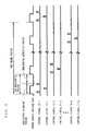
- FIG. 6 A timing chart showing the above-described operations is as shown in FIG. 6.
- the period during which signals accumulated in photodiodes 51 for one row are finally outputted from the output terminal 70 is called a horizontal effective period
- the period during which the signals are outputted from the photodiodes 51 to the vertical signal lines 62 and the noise of the outputted signals is suppressed is called a horizontal blanking period.
- the horizontal blanking period and the horizontal effective period are together called one horizontal period.
- the one horizontal period is the time actually required to read signals for one row.
- the time required to read signals from the entire sensor is called one frame period. As shown in FIG.
- the amount of a signal charge accumulated in the photodiode 51 is determined by the time interval of a transfer pulse to be applied to the transfer gate 52.
- the time interval of the transfer pulse is constant during one frame period. Therefore, the photodiodes 51 have uniform sensitivity.
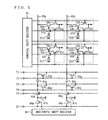
- pairs of m signals lines 17-1 to 17-m and 18-1 to 18-m are wired in addition to the power supply line 10 and the vertical signal lines 12-1 to 12-n.
- the power supply line 10 is commonly connected to drains of the amplifying transistors 4.
- the present embodiment assumes that the power supply line 10 is commonly connected to the drains of the amplifying transistors 4 and the reset transistors 5 included in all the photosensitive cells, and a pulsed power supply voltage VddC is applied to all the photosensitive cells from a power supply terminal 20 which is present at the other end of the power supply line 10. Note that although, in FIG. 1, all the photosensitive cells are connected to the single power supply line 10, two or more power supply lines may be used to supply a common power supply to the photosensitive cells.
- a power supply voltage VddC is at a low level. That is, in the initial state, the power supply line 10 is not yet driven.
- the power supply voltage VddC is controlled to be at a high level. By this, in all the photosensitive cells, the drains of the transfer gates 2 and the reset transistors 5 are brought to a high level. Then, while the power supply line 10 is driven, the vertical shift register 11 brings the signal line 18-1 to a high level for a predetermined period of time.
- the gate potentials of the reset transistors 5a and 5b and all other reset transistors 5 included in the photosensitive cells in the first row are brought to a high level, and these reset transistors 5 are brought into an ON state.
- the amplifying transistors 4a and 4b and all other amplifying transistors 4 included in the photosensitive cells in the first row are brought into an operation state.
- noise outputs which are generated when signal charges accumulated in the floating diffusion layer portions 3a and 3b and all other floating diffusion layer portions 3 included in the photosensitive cells in the first row are reset, appear on the vertical signal lines 12-1 to 12-n.
Landscapes
- Engineering & Computer Science (AREA)
- Multimedia (AREA)
- Signal Processing (AREA)
- Physics & Mathematics (AREA)
- Electromagnetism (AREA)
- Solid State Image Pick-Up Elements (AREA)
- Transforming Light Signals Into Electric Signals (AREA)
Applications Claiming Priority (3)
| Application Number | Priority Date | Filing Date | Title |
|---|---|---|---|
| JP2003054589A JP4355148B2 (ja) | 2003-02-28 | 2003-02-28 | 固体撮像装置の駆動方法 |
| JP2003054589 | 2003-02-28 | ||
| PCT/JP2004/002282 WO2004077822A1 (ja) | 2003-02-28 | 2004-02-26 | 固体撮像装置の駆動方法 |
Publications (2)
| Publication Number | Publication Date |
|---|---|
| EP1599039A1 true EP1599039A1 (de) | 2005-11-23 |
| EP1599039A4 EP1599039A4 (de) | 2006-05-03 |
Family
ID=32923467
Family Applications (1)
| Application Number | Title | Priority Date | Filing Date |
|---|---|---|---|
| EP04714932A Withdrawn EP1599039A4 (de) | 2003-02-28 | 2004-02-26 | Ansteuerverfahren f r eine r hrenlose abbildungseinrichutng |
Country Status (7)
| Country | Link |
|---|---|
| US (5) | US7352399B2 (de) |
| EP (1) | EP1599039A4 (de) |
| JP (1) | JP4355148B2 (de) |
| KR (1) | KR100990608B1 (de) |
| CN (1) | CN100349460C (de) |
| TW (1) | TWI330888B (de) |
| WO (1) | WO2004077822A1 (de) |
Cited By (1)
| Publication number | Priority date | Publication date | Assignee | Title |
|---|---|---|---|---|
| EP1940148A3 (de) * | 2006-12-28 | 2010-07-28 | Canon Kabushiki Kaisha | Festkörperbildsensor und Abbildungssystem |
Families Citing this family (20)
| Publication number | Priority date | Publication date | Assignee | Title |
|---|---|---|---|---|
| JP4355148B2 (ja) * | 2003-02-28 | 2009-10-28 | パナソニック株式会社 | 固体撮像装置の駆動方法 |
| US7355228B2 (en) | 2004-10-15 | 2008-04-08 | Omnivision Technologies, Inc. | Image sensor pixel having photodiode with multi-dopant implantation |
| US7382008B2 (en) * | 2006-05-02 | 2008-06-03 | Eastman Kodak Company | Ultra-small CMOS image sensor pixel using a photodiode potential technique |
| JP2008005155A (ja) * | 2006-06-21 | 2008-01-10 | Sharp Corp | 増幅型固体撮像装置およびその駆動方法、電子情報機器 |
| JP4185949B2 (ja) * | 2006-08-08 | 2008-11-26 | キヤノン株式会社 | 光電変換装置及び撮像装置 |
| JP4305516B2 (ja) * | 2007-01-30 | 2009-07-29 | ソニー株式会社 | 固体撮像素子及び固体撮像装置 |
| JP5016941B2 (ja) | 2007-02-08 | 2012-09-05 | 株式会社東芝 | 固体撮像装置 |
| JP4058459B1 (ja) * | 2007-03-02 | 2008-03-12 | キヤノン株式会社 | 撮像装置及び撮像システム |
| JP2010200025A (ja) * | 2009-02-25 | 2010-09-09 | Panasonic Corp | 固体撮像装置 |
| JP5238673B2 (ja) * | 2009-11-09 | 2013-07-17 | 株式会社東芝 | 固体撮像装置 |
| JP4921615B2 (ja) | 2010-01-25 | 2012-04-25 | パナソニック株式会社 | プロテインaを自己組織化膜上に固定する方法 |
| JP5149992B2 (ja) | 2010-08-30 | 2013-02-20 | パナソニック株式会社 | ストレプトアビジンを自己組織化膜上に固定する方法 |
| US20120049041A1 (en) * | 2010-09-01 | 2012-03-01 | International Business Machines Corporation | Switched rail circuitry and modified cell structure and method of manufacture and use |
| CN103124786A (zh) | 2010-10-19 | 2013-05-29 | 松下电器产业株式会社 | 将葡萄糖氧化酶固定在自组装膜上的方法 |
| JP6021360B2 (ja) * | 2012-03-07 | 2016-11-09 | キヤノン株式会社 | 撮像装置、撮像システム、および撮像装置の駆動方法。 |
| WO2014002365A1 (ja) * | 2012-06-26 | 2014-01-03 | パナソニック株式会社 | 固体撮像装置及びその製造方法 |
| KR102083776B1 (ko) * | 2013-09-03 | 2020-04-16 | 삼성전자 주식회사 | 조도 변화에 따라 다른 전압을 픽셀들로 공급할 수 있는 이미지 센서, 이의 동작 방법, 및 상기 이미지 센서를 포함하는 장치 |
| WO2016002257A1 (ja) * | 2014-07-02 | 2016-01-07 | オリンパス株式会社 | 撮像素子、撮像装置、内視鏡、内視鏡システムおよび撮像素子の駆動方法 |
| CN104698773B (zh) * | 2015-03-31 | 2017-06-16 | 上海华力微电子有限公司 | 光刻对准标记结构及其制造方法 |
| WO2018143295A1 (ja) | 2017-01-31 | 2018-08-09 | 株式会社ニコン | 撮像素子および撮像装置 |
Family Cites Families (34)
| Publication number | Priority date | Publication date | Assignee | Title |
|---|---|---|---|---|
| JPH07255013A (ja) * | 1994-01-31 | 1995-10-03 | Sony Corp | 固体撮像装置 |
| JP3385760B2 (ja) * | 1994-02-21 | 2003-03-10 | ソニー株式会社 | 固体撮像装置及びその駆動方法 |
| JP3695827B2 (ja) | 1996-03-13 | 2005-09-14 | 株式会社東芝 | 固体撮像装置 |
| JP3579194B2 (ja) * | 1996-09-17 | 2004-10-20 | 株式会社東芝 | 固体撮像装置の駆動方法 |
| US6037577A (en) * | 1997-03-11 | 2000-03-14 | Kabushiki Kaisha Toshiba | Amplifying solid-state image pickup device and operating method of the same |
| JPH10257392A (ja) * | 1997-03-14 | 1998-09-25 | Matsushita Electron Corp | 物理量分布検知半導体装置およびその駆動方法ならびにその製造方法 |
| US5969758A (en) * | 1997-06-02 | 1999-10-19 | Sarnoff Corporation | DC offset and gain correction for CMOS image sensor |
| US6115066A (en) * | 1997-06-12 | 2000-09-05 | International Business Machines Corporation | Image sensor with direct digital correlated sampling |
| US6344877B1 (en) * | 1997-06-12 | 2002-02-05 | International Business Machines Corporation | Image sensor with dummy pixel or dummy pixel array |
| JP3466886B2 (ja) * | 1997-10-06 | 2003-11-17 | キヤノン株式会社 | 固体撮像装置 |
| JPH11261046A (ja) * | 1998-03-12 | 1999-09-24 | Canon Inc | 固体撮像装置 |
| JP4200545B2 (ja) * | 1998-06-08 | 2008-12-24 | ソニー株式会社 | 固体撮像素子およびその駆動方法、並びにカメラシステム |
| JP3621844B2 (ja) * | 1999-02-24 | 2005-02-16 | シャープ株式会社 | 増幅型固体撮像装置 |
| JP2001045375A (ja) | 1999-08-03 | 2001-02-16 | Canon Inc | 撮像装置とその読み出し方法 |
| JP3667186B2 (ja) * | 2000-02-29 | 2005-07-06 | キヤノン株式会社 | 信号転送装置及びそれを用いた固体撮像装置 |
| US6958776B2 (en) * | 2000-07-12 | 2005-10-25 | Vanguard International Semiconductor Corp. | Method and apparatus of controlling a pixel reset level for reducing an image lag in a CMOS sensor |
| JP3750502B2 (ja) * | 2000-08-03 | 2006-03-01 | ソニー株式会社 | 固体撮像装置およびカメラシステム |
| JP3628970B2 (ja) | 2001-02-08 | 2005-03-16 | 松下電器産業株式会社 | 固体撮像装置及びその駆動方法 |
| JP4681767B2 (ja) * | 2001-07-17 | 2011-05-11 | キヤノン株式会社 | 撮像装置およびカメラ |
| EP1459356A2 (de) * | 2001-12-21 | 2004-09-22 | Koninklijke Philips Electronics N.V. | Bildaufnahmevorrichtung und kamerasystem dass eine bildaufnahmevorrichtung enthält |
| JP3921093B2 (ja) * | 2002-01-29 | 2007-05-30 | シャープ株式会社 | 増幅型固体撮像装置 |
| JP4164733B2 (ja) * | 2002-02-05 | 2008-10-15 | ソニー株式会社 | 固体撮像装置及びその駆動方法 |
| JP4132850B2 (ja) * | 2002-02-06 | 2008-08-13 | 富士通株式会社 | Cmosイメージセンサおよびその制御方法 |
| JP4193698B2 (ja) * | 2002-02-12 | 2008-12-10 | ソニー株式会社 | 固体撮像装置およびカメラシステム |
| JP2003264745A (ja) * | 2002-03-08 | 2003-09-19 | Sanyo Electric Co Ltd | 電荷転送装置 |
| JP3969190B2 (ja) * | 2002-05-30 | 2007-09-05 | ソニー株式会社 | 撮像信号処理方法、撮像信号処理装置、撮像装置 |
| JP2004172679A (ja) * | 2002-11-15 | 2004-06-17 | Matsushita Electric Ind Co Ltd | 撮像装置 |
| JP3988189B2 (ja) * | 2002-11-20 | 2007-10-10 | ソニー株式会社 | 固体撮像装置 |
| JP4355148B2 (ja) * | 2003-02-28 | 2009-10-28 | パナソニック株式会社 | 固体撮像装置の駆動方法 |
| JP4297416B2 (ja) * | 2003-06-10 | 2009-07-15 | シャープ株式会社 | 固体撮像素子、その駆動方法およびカメラ |
| JP2005347793A (ja) * | 2004-05-31 | 2005-12-15 | Matsushita Electric Ind Co Ltd | 撮像装置 |
| JP2006019343A (ja) * | 2004-06-30 | 2006-01-19 | Pentax Corp | 固体撮像素子 |
| JP4979195B2 (ja) * | 2005-02-21 | 2012-07-18 | ソニー株式会社 | 固体撮像素子、固体撮像素子の駆動方法および撮像装置 |
| JP2007180654A (ja) * | 2005-12-27 | 2007-07-12 | Matsushita Electric Ind Co Ltd | 撮像装置 |
-
2003
- 2003-02-28 JP JP2003054589A patent/JP4355148B2/ja not_active Expired - Fee Related
-
2004
- 2004-02-26 EP EP04714932A patent/EP1599039A4/de not_active Withdrawn
- 2004-02-26 US US10/532,992 patent/US7352399B2/en not_active Expired - Fee Related
- 2004-02-26 KR KR1020057009741A patent/KR100990608B1/ko not_active Expired - Fee Related
- 2004-02-26 CN CNB2004800012785A patent/CN100349460C/zh not_active Expired - Fee Related
- 2004-02-26 WO PCT/JP2004/002282 patent/WO2004077822A1/ja not_active Ceased
- 2004-02-27 TW TW093105048A patent/TWI330888B/zh not_active IP Right Cessation
-
2008
- 2008-02-15 US US12/071,090 patent/US7714920B2/en not_active Expired - Lifetime
-
2009
- 2009-08-06 US US12/536,829 patent/US8274590B2/en not_active Expired - Fee Related
- 2009-08-06 US US12/536,814 patent/US8253833B2/en not_active Expired - Fee Related
-
2012
- 2012-08-23 US US13/592,792 patent/US20130021509A1/en not_active Abandoned
Cited By (3)
| Publication number | Priority date | Publication date | Assignee | Title |
|---|---|---|---|---|
| EP1940148A3 (de) * | 2006-12-28 | 2010-07-28 | Canon Kabushiki Kaisha | Festkörperbildsensor und Abbildungssystem |
| US7825974B2 (en) | 2006-12-28 | 2010-11-02 | Canon Kabushiki Kaisha | Solid-state image sensor and imaging system |
| US8063967B2 (en) | 2006-12-28 | 2011-11-22 | Canon Kabushiki Kaisha | Solid-state image sensor and imaging system |
Also Published As
| Publication number | Publication date |
|---|---|
| US20130021509A1 (en) | 2013-01-24 |
| CN100349460C (zh) | 2007-11-14 |
| KR100990608B1 (ko) | 2010-10-29 |
| KR20050109456A (ko) | 2005-11-21 |
| TWI330888B (en) | 2010-09-21 |
| US20090322924A1 (en) | 2009-12-31 |
| US20090295961A1 (en) | 2009-12-03 |
| US7714920B2 (en) | 2010-05-11 |
| US20080143861A1 (en) | 2008-06-19 |
| US7352399B2 (en) | 2008-04-01 |
| US20060050161A1 (en) | 2006-03-09 |
| US8274590B2 (en) | 2012-09-25 |
| JP4355148B2 (ja) | 2009-10-28 |
| WO2004077822A1 (ja) | 2004-09-10 |
| JP2004266565A (ja) | 2004-09-24 |
| TW200501404A (en) | 2005-01-01 |
| US8253833B2 (en) | 2012-08-28 |
| EP1599039A4 (de) | 2006-05-03 |
| CN1706182A (zh) | 2005-12-07 |
Similar Documents
| Publication | Publication Date | Title |
|---|---|---|
| US8274590B2 (en) | Solid-state imaging device driving method | |
| KR101045117B1 (ko) | 고체 촬상 장치 | |
| US7511275B2 (en) | Semiconductor device, and control method and device for driving unit component of semiconductor device | |
| US8120682B2 (en) | Solid-state image pickup device and method of resetting the same | |
| US20180054576A1 (en) | Solid-state imaging device, method for driving solid-state imaging device, and electronic apparatus | |
| JP4288346B2 (ja) | 撮像装置及び画素回路 | |
| JPH11122532A (ja) | 固体撮像素子およびその駆動方法 | |
| JP2010103494A (ja) | 固体撮像装置とその駆動方法、並びに電子機器 | |
| US8823069B2 (en) | Solid-state imaging device, drive method of solid-state imaging device, and imaging apparatus | |
| US7906752B2 (en) | Solid-state imaging apparatus | |
| JP2708455B2 (ja) | 固体撮像装置 | |
| JP2007104386A (ja) | 固体撮像装置および撮像装置 | |
| WO2008010893A2 (en) | Method, apparatus and system for charge injection suppression in active pixel sensors | |
| JP4336544B2 (ja) | 固体撮像装置 | |
| JP2004048813A (ja) | 固体撮像装置 | |
| JP4156424B2 (ja) | 固体撮像装置の駆動方法 | |
| JP2009081634A (ja) | 固体撮像装置及びその制御方法 | |
| JP4330579B2 (ja) | 固体撮像装置 | |
| JPH1093863A (ja) | 固体撮像素子及びその駆動方法、並びにスチルカメラ |
Legal Events
| Date | Code | Title | Description |
|---|---|---|---|
| PUAI | Public reference made under article 153(3) epc to a published international application that has entered the european phase |
Free format text: ORIGINAL CODE: 0009012 |
|
| 17P | Request for examination filed |
Effective date: 20050726 |
|
| AK | Designated contracting states |
Kind code of ref document: A1 Designated state(s): AT BE BG CH CY CZ DE DK EE ES FI FR GB GR HU IE IT LI LU MC NL PT RO SE SI SK TR |
|
| AX | Request for extension of the european patent |
Extension state: AL LT LV MK |
|
| A4 | Supplementary search report drawn up and despatched |
Effective date: 20060317 |
|
| DAX | Request for extension of the european patent (deleted) | ||
| RBV | Designated contracting states (corrected) |
Designated state(s): DE FR GB |
|
| 17Q | First examination report despatched |
Effective date: 20071030 |
|
| RAP1 | Party data changed (applicant data changed or rights of an application transferred) |
Owner name: PANASONIC CORPORATION |
|
| STAA | Information on the status of an ep patent application or granted ep patent |
Free format text: STATUS: THE APPLICATION IS DEEMED TO BE WITHDRAWN |
|
| 18D | Application deemed to be withdrawn |
Effective date: 20090829 |