WO2018143295A1 - 撮像素子および撮像装置 - Google Patents
撮像素子および撮像装置 Download PDFInfo
- Publication number
- WO2018143295A1 WO2018143295A1 PCT/JP2018/003278 JP2018003278W WO2018143295A1 WO 2018143295 A1 WO2018143295 A1 WO 2018143295A1 JP 2018003278 W JP2018003278 W JP 2018003278W WO 2018143295 A1 WO2018143295 A1 WO 2018143295A1
- Authority
- WO
- WIPO (PCT)
- Prior art keywords
- unit
- output
- photoelectric conversion
- signal
- storage unit
- Prior art date
Links
- 238000003384 imaging method Methods 0.000 title claims abstract description 56
- 238000006243 chemical reaction Methods 0.000 claims abstract description 137
- 238000009825 accumulation Methods 0.000 claims abstract description 86
- 238000012546 transfer Methods 0.000 claims description 42
- 230000003321 amplification Effects 0.000 claims description 40
- 238000003199 nucleic acid amplification method Methods 0.000 claims description 40
- 239000003990 capacitor Substances 0.000 claims description 2
- 238000000034 method Methods 0.000 description 30
- 238000012545 processing Methods 0.000 description 19
- 238000001514 detection method Methods 0.000 description 15
- 238000012986 modification Methods 0.000 description 12
- 230000004048 modification Effects 0.000 description 12
- 230000003287 optical effect Effects 0.000 description 11
- 238000010586 diagram Methods 0.000 description 10
- 101100191136 Arabidopsis thaliana PCMP-A2 gene Proteins 0.000 description 8
- 101100048260 Saccharomyces cerevisiae (strain ATCC 204508 / S288c) UBX2 gene Proteins 0.000 description 8
- 230000000875 corresponding effect Effects 0.000 description 7
- 101100422768 Saccharomyces cerevisiae (strain ATCC 204508 / S288c) SUL2 gene Proteins 0.000 description 6
- 230000002596 correlated effect Effects 0.000 description 4
- 210000001747 pupil Anatomy 0.000 description 4
- 238000005070 sampling Methods 0.000 description 4
- 230000000052 comparative effect Effects 0.000 description 3
- 230000006870 function Effects 0.000 description 3
- 230000007423 decrease Effects 0.000 description 2
- 238000012935 Averaging Methods 0.000 description 1
- 238000012937 correction Methods 0.000 description 1
- 230000003247 decreasing effect Effects 0.000 description 1
- 230000000694 effects Effects 0.000 description 1
- 230000004907 flux Effects 0.000 description 1
- 239000011159 matrix material Substances 0.000 description 1
- 230000003071 parasitic effect Effects 0.000 description 1
Images


Classifications
-
- H—ELECTRICITY
- H04—ELECTRIC COMMUNICATION TECHNIQUE
- H04N—PICTORIAL COMMUNICATION, e.g. TELEVISION
- H04N25/00—Circuitry of solid-state image sensors [SSIS]; Control thereof
- H04N25/40—Extracting pixel data from image sensors by controlling scanning circuits, e.g. by modifying the number of pixels sampled or to be sampled
- H04N25/46—Extracting pixel data from image sensors by controlling scanning circuits, e.g. by modifying the number of pixels sampled or to be sampled by combining or binning pixels
-
- H—ELECTRICITY
- H04—ELECTRIC COMMUNICATION TECHNIQUE
- H04N—PICTORIAL COMMUNICATION, e.g. TELEVISION
- H04N23/00—Cameras or camera modules comprising electronic image sensors; Control thereof
- H04N23/60—Control of cameras or camera modules
- H04N23/67—Focus control based on electronic image sensor signals
- H04N23/672—Focus control based on electronic image sensor signals based on the phase difference signals
-
- H—ELECTRICITY
- H04—ELECTRIC COMMUNICATION TECHNIQUE
- H04N—PICTORIAL COMMUNICATION, e.g. TELEVISION
- H04N23/00—Cameras or camera modules comprising electronic image sensors; Control thereof
- H04N23/60—Control of cameras or camera modules
- H04N23/667—Camera operation mode switching, e.g. between still and video, sport and normal or high- and low-resolution modes
-
- H—ELECTRICITY
- H04—ELECTRIC COMMUNICATION TECHNIQUE
- H04N—PICTORIAL COMMUNICATION, e.g. TELEVISION
- H04N25/00—Circuitry of solid-state image sensors [SSIS]; Control thereof
- H04N25/70—SSIS architectures; Circuits associated therewith
- H04N25/703—SSIS architectures incorporating pixels for producing signals other than image signals
- H04N25/704—Pixels specially adapted for focusing, e.g. phase difference pixel sets
-
- H—ELECTRICITY
- H04—ELECTRIC COMMUNICATION TECHNIQUE
- H04N—PICTORIAL COMMUNICATION, e.g. TELEVISION
- H04N25/00—Circuitry of solid-state image sensors [SSIS]; Control thereof
- H04N25/70—SSIS architectures; Circuits associated therewith
- H04N25/71—Charge-coupled device [CCD] sensors; Charge-transfer registers specially adapted for CCD sensors
- H04N25/75—Circuitry for providing, modifying or processing image signals from the pixel array
-
- H—ELECTRICITY
- H04—ELECTRIC COMMUNICATION TECHNIQUE
- H04N—PICTORIAL COMMUNICATION, e.g. TELEVISION
- H04N25/00—Circuitry of solid-state image sensors [SSIS]; Control thereof
- H04N25/70—SSIS architectures; Circuits associated therewith
- H04N25/76—Addressed sensors, e.g. MOS or CMOS sensors
- H04N25/77—Pixel circuitry, e.g. memories, A/D converters, pixel amplifiers, shared circuits or shared components
-
- H—ELECTRICITY
- H04—ELECTRIC COMMUNICATION TECHNIQUE
- H04N—PICTORIAL COMMUNICATION, e.g. TELEVISION
- H04N25/00—Circuitry of solid-state image sensors [SSIS]; Control thereof
- H04N25/70—SSIS architectures; Circuits associated therewith
- H04N25/76—Addressed sensors, e.g. MOS or CMOS sensors
- H04N25/78—Readout circuits for addressed sensors, e.g. output amplifiers or A/D converters
Definitions
- the present invention relates to an imaging element and an imaging apparatus.
- Patent Document 1 There is known an imaging device that adds (mixes) the charges of two light receiving elements and reads a potential corresponding to the added charge (Patent Document 1).
- Patent Document 1 An imaging device that adds (mixes) the charges of two light receiving elements and reads a potential corresponding to the added charge.
- Patent Document 1 the conventional imaging device has a problem that the conversion gain when converting the added charge into the potential is small.
- the imaging device includes a first photoelectric conversion unit that photoelectrically converts light to generate charges, and a first charge that accumulates charges generated by the first photoelectric conversion unit.
- a first pixel having a storage unit and a first output unit connected to the first storage unit; a second photoelectric conversion unit that photoelectrically converts light to generate a charge; and A second pixel having a second accumulation unit that accumulates charges generated by the photoelectric conversion unit, and a second output unit that is disconnected through the second accumulation unit and the second connection unit; ,
- An adjustment unit for adjusting the capacity is provided to generate charges, and a first charge that accumulates charges generated by the first photoelectric conversion unit.
- the imaging device includes a first photoelectric conversion unit that photoelectrically converts light to generate charges, and a first charge that accumulates charges generated by the first photoelectric conversion unit.
- a first pixel having a storage unit, a first output unit connected to the first storage unit via the first connection unit, and a second photoelectric unit that photoelectrically converts light to generate a charge.
- a second pixel includes the imaging element according to the first or second aspect, and an image generation unit that generates image data based on a signal output from the imaging element.
- FIG. 3 is a circuit diagram illustrating a configuration of a pixel according to the first embodiment.
- FIG. 6 is a diagram for explaining an operation example of the image sensor according to the first embodiment. The figure for demonstrating another operation example of the image pick-up element which concerns on 1st Embodiment.
- FIG. 2 is a circuit diagram showing a configuration of a part of the image sensor according to the first embodiment. 3 is a timing chart showing an operation example of the image sensor according to the first embodiment. 6 is a timing chart showing another operation example of the image sensor according to the first embodiment. 6 is a timing chart showing another operation example of the image sensor according to the first embodiment.
- FIG. 1 is a block diagram illustrating a configuration of the imaging apparatus according to the first embodiment.
- FIG. 1 shows a configuration example of an electronic camera 1 (hereinafter referred to as camera 1) which is an example of an imaging apparatus according to the first embodiment.
- the camera 1 includes an imaging optical system (imaging optical system) 2, an imaging element 3, a control unit 4, a memory 5, a display unit 6, and an operation unit 7.
- the imaging optical system 2 has a plurality of lenses including a focus adjustment lens (focus lens) and an aperture, and forms a subject image on the imaging element 3. Note that the imaging optical system 2 may be detachable from the camera 1.
- the image sensor 3 is, for example, a CMOS image sensor.
- the imaging element 3 receives the light beam that has passed through the exit pupil of the imaging optical system 2 and captures a subject image.
- the imaging element 3 has a plurality of pixels having a microlens and a plurality of photoelectric conversion units (for example, two photoelectric conversion units) in a two-dimensional shape (row direction and column direction intersecting therewith). Placed in.
- the photoelectric conversion unit is configured by, for example, a photodiode (PD).
- PD photodiode
- the image sensor 3 photoelectrically converts incident light to generate a signal, and outputs the generated signal to the control unit 4.
- the imaging element 3 has a signal for generating image data, that is, an imaging signal, and a pair of focus detection signals for performing phase-difference focus detection on the focus of the imaging optical system 2, that is, first and first. 2 focus detection signals are output to the control unit 4.
- the first and second focus detection signals photoelectrically convert the first and second images of the first and second light beams that have passed through the first and second regions of the exit pupil of the imaging optical system 2, respectively. Signal.
- the memory 5 is a recording medium such as a memory card, for example. Image data and the like are recorded in the memory 5. Writing of data to the memory 5 and reading of data from the memory 5 are performed by the control unit 4.
- the display unit 6 displays an image based on image data, information relating to shooting such as a shutter speed and an aperture value, a menu screen, and the like.
- the operation unit 7 includes various setting switches such as a release button and a power switch, and outputs an operation signal corresponding to each operation to the control unit 4.
- the control unit 4 includes a CPU, a ROM, a RAM, and the like, and controls each unit of the camera 1 based on a control program.
- the control unit 4 includes an image data generation unit 4a and a focus detection unit 4b.
- the image data generation unit 4a performs various kinds of image processing on the imaging signal output from the imaging device 3 to generate image data.
- the image processing includes, for example, known image processing such as gradation conversion processing, color interpolation processing, and contour enhancement processing.
- the focus detection unit 4b performs a focus detection process necessary for automatic focus adjustment (AF) of the imaging optical system 2 by a known phase difference detection method. Specifically, the focus detection unit 4b detects the image shift amounts of the first and second images based on the pair of focus detection signals output from the image sensor 3, and the defocus amount is detected based on the detected image shift amounts. Calculate the focus amount. The focus adjustment is automatically performed by driving the focus adjustment lens according to the defocus amount.
- the control unit 4 individually reads signals from the plurality of photoelectric conversion units of each pixel of the image sensor 3 (first control mode), and adds and reads signals from the plurality of photoelectric conversion units (first control mode). 2 control mode).
- first control mode a signal based on the charge generated by the first photoelectric conversion unit and a signal based on the charge generated by the second photoelectric conversion unit are Read out individually, that is, independently as a pair of focus detection signals.
- the control unit 4 performs a process of adding signals from each of the first and second photoelectric conversion units and reads out as an imaging signal.
- the “adding process” includes a process of averaging a plurality of signals, a process of weighting and adding a plurality of signals, and the like.
- the controller 4 performs the first control mode when performing phase difference AF, reads a pair of focus detection signals from the image sensor 3, and performs the second control mode when generating image data. An imaging signal is read from the imaging element 3.
- FIG. 2 is a circuit diagram showing the configuration of the pixels of the image sensor 3 according to the first embodiment.
- the pixel 10 includes a micro lens ML, a first photoelectric conversion unit 11a, a second photoelectric conversion unit 11b, a first transfer unit 12a, a second transfer unit 12b, and a first reset unit 13a.
- the pixel 10 further includes a first amplification unit 15a, a second amplification unit 15b, a first selection unit 16a, a second selection unit 16b, an addition switch unit 17, and a first connection switch unit. 19a, 2nd connection switch part 19b, 1st area
- the microlens ML condenses the light incident through the imaging optical system 2 of FIG. 1 on the first photoelectric conversion unit 11a and the second photoelectric conversion unit 11b.
- the microlens ML surrounds the first and second photoelectric conversion units 11a and 11b in order to indicate that the light beam that has passed through the microlens ML is incident on the first and second photoelectric conversion units 11a and 11b. It is indicated by an oval line. This elliptical shape does not represent the actual size or actual shape of the microlens ML.
- the first photoelectric conversion unit 11a and the second photoelectric conversion unit 11b are photodiodes PD (PDa, PDb), and have a function of converting incident light into charges and accumulating the photoelectrically converted charges.
- the first photoelectric conversion unit 11 a and the second photoelectric conversion unit 11 b are arranged corresponding to one microlens ML, and receive light beams that have passed through different regions of the exit pupil of the imaging optical system 2. That is, the first photoelectric conversion unit 11a and the second photoelectric conversion unit 11b are the first and second light fluxes that have passed through the first and second regions of the exit pupil of the imaging optical system 2, respectively. Each of the two images is photoelectrically converted.
- the first transfer unit 12a includes a transistor M1a controlled by a signal TX1.
- the first transfer unit 12a transfers the charge photoelectrically converted by the first photoelectric conversion unit 11a to the first accumulation unit 14a. That is, the first transfer unit 12a forms a charge transfer path between the first photoelectric conversion unit 11a and the first storage unit 14a.
- the transistor M9a of the first connection switch unit 19a is on, the first transfer unit 12a uses the first storage unit 14a and the first storage unit 14a to store the charge photoelectrically converted by the first photoelectric conversion unit 11a.
- the transistor M1a is a first transfer transistor.
- Capacitance such as capacitance (parasitic capacitance) of each transistor connected to the first accumulation unit 14a and wiring capacitance is added to the first accumulation unit 14a.
- the first accumulation unit 14a accumulates (holds) the charge transferred to the first accumulation unit 14a, and converts the charge into a voltage divided by the capacitance value.
- the first connection switch unit 19a includes a transistor M9a controlled by a signal ADD_FD1, and connects (couples) the first storage unit 14a and the first amplification unit 15a. It can also be said that the first connection switch unit 19a connects the first storage unit 14a and the first region 20a.
- the capacity of each transistor such as the gate capacity of the first amplifying unit 15a connected to the first area 20a and the capacity of the wiring capacity are added to the first area 20a.
- the first region 20a accumulates the charge transferred to the first region 20a and converts it into a voltage divided by the capacitance value.
- the first amplifying unit 15a amplifies and outputs a signal based on the charge transferred from the photoelectric conversion unit.
- the first amplifying unit 15a includes a transistor M3a.
- the drain (terminal) of the transistor M3a is connected to the power supply VDD, and the gate (terminal) of the transistor M3a is connected to the drain of the transistor M9a of the first connection switch unit 19a.
- the source (terminal) of the transistor M3a is connected to the transistor M4a of the first selection unit 16a.
- the source of the transistor M3a of the first amplifier 15a is connected to the first vertical signal line VLa via the first selector 16a.
- the first amplifying unit 15a functions as a part of the source follower circuit using the first current source 25a shown in FIG. 3 as a load current source.
- the transistor M3a is a first amplification transistor.
- the first reset unit 13a includes a transistor M2a controlled by a signal RS1, resets the charges in the first region 20a and the first storage unit 14a, and the first region 20a and the first storage unit 14a. Reset the voltage.
- the transistor M2a is a first reset transistor.
- the first selection unit 16a includes a transistor M4a controlled by the signal SEL1, and outputs a signal from the first amplification unit 15a to the first vertical signal line VLa.
- the transistor M4a is a first selection transistor.
- the first output unit according to the present embodiment includes a first amplifying unit 15a, a first selecting unit 16a, and a first reset unit 13a, and the charge generated by the first photoelectric conversion unit 11a Generate and output a signal based on it.
- the second transfer unit 12b includes a transistor M1b controlled by a signal TX2.
- the second transfer unit 12b transfers the charge photoelectrically converted by the second photoelectric conversion unit 11b to the second accumulation unit 14b. That is, the second transfer unit 12b forms a charge transfer path between the second photoelectric conversion unit 11b and the second storage unit 14b.
- the transistor M9b of the second connection switch unit 19b is on, the second transfer unit 12b uses the second storage unit 14b and the second storage unit 14b to store the charges photoelectrically converted by the second photoelectric conversion unit 11b.
- the transistor M1b is a second transfer transistor.
- Capacities such as the capacitance of each transistor connected to the second storage unit 14b and the wiring capacity are added to the second storage unit 14b.
- the second storage unit 14b stores the charge transferred to the second storage unit 14b, and converts the charge into a voltage divided by the capacitance value.
- the second connection switch unit 19b includes a transistor M9b controlled by the signal ADD_FD2, and connects the second accumulation unit 14b and the second amplification unit 15b. It can also be said that the second connection switch unit 19b connects the second storage unit 14b and the second region 20b.
- the capacity of each transistor such as the gate capacity of the second amplifying unit 15b connected to the second area 20b and the capacity of the wiring capacity are added to the second area 20b.
- the second region 20b accumulates the charge transferred to the second region 20b and converts it into a voltage divided by the capacitance value.
- the second amplification unit 15b amplifies and outputs a signal based on the charge transferred from the photoelectric conversion unit.
- the second amplifying unit 15b includes a transistor M3b.
- the drain of the transistor M3b is connected to the power supply VDD, and the gate of the transistor M3b is connected to the drain of the transistor M9b of the second connection switch unit 19b.
- the source of the transistor M3b is connected to the transistor M4b of the second selection unit 16b.
- the source of the second amplification unit 15b is connected to the second vertical signal line VLb through the second selection unit 16b.
- the second amplifying unit 15b functions as a part of the source follower circuit using the second current source 25b shown in FIG. 3 as a load current source.
- the transistor M3b is a second amplification transistor.
- the second reset unit 13b includes a transistor M2b controlled by the signal RS2, resets the charges in the second region 20b and the second storage unit 14b, and the second region 20b and the second storage unit 14b. Reset the voltage.
- the transistor M2b is a second reset transistor.
- the second selection unit 16b includes a transistor M4b controlled by the signal SEL2, and outputs a signal from the second amplification unit 15b to the second vertical signal line VLb.
- the transistor M4b is a second selection transistor.
- the second output unit according to the present embodiment includes a second amplification unit 15b, a second selection unit 16b, and a second reset unit 13b, and the charge generated by the second photoelectric conversion unit 11b Generate and output a signal based on it.
- the addition switch unit 17 includes a transistor M7 controlled by a signal ADD_FD3, and connects the first storage unit 14a and the second storage unit 14b. It can also be said that the addition switch unit 17 connects the first transfer unit 12a and the second transfer unit 12b.
- the control unit 4 controls the imaging device 3 to turn off (state) the transistor M7 of the addition switch unit 17, turn on the transistor M9a of the first connection switch unit 19a, and perform the second connection.
- the transistor M9b of the switch unit 19b is turned on.
- the electric charge photoelectrically converted by the first photoelectric conversion unit 11a is transferred to the first accumulation unit 14a and the first region 20a.
- a signal (first pixel signal) corresponding to the charge transferred from the first photoelectric conversion unit 11a is read out to the first vertical signal line VLa by the first amplification unit 15a and the first selection unit 16a. It is.
- the electric charge photoelectrically converted by the second photoelectric conversion unit 11b is transferred to the second accumulation unit 14b and the second region 20b.
- a signal (second pixel signal) corresponding to the charge transferred from the second photoelectric conversion unit 11b is read out to the second vertical signal line VLb by the second amplification unit 15b and the second selection unit 16b.
- the first pixel signal generated according to the charge from the first photoelectric conversion unit 11a is output to the first vertical signal line VLa, and the second photoelectric conversion unit.
- the second pixel signal generated according to the charge from 11b is output to the second vertical signal line VLb.
- the first pixel signal and the second pixel signal are output to the control unit 4 as a pair of focus detection signals after being subjected to signal processing by a column circuit or the like which will be described later.
- the control unit 4 turns on the transistor M7 of the addition switch unit 17.
- the control unit 4 turns on the transistor M9a of the first connection switch unit 19a, turns off the transistor M9b of the second connection switch unit 19b, turns on the transistor M4a of the first selection unit 16a, and turns on the second selection unit.
- the transistor M4b of 16b is turned off.
- the charges photoelectrically converted by the first and second photoelectric conversion units 11a and 11b are transferred by the first and second transfer units 12a and 12b, respectively, and added by the addition switch unit 17.
- the first amplifying unit 15a and the first selecting unit 16a generate an added pixel signal according to the added charge and read it out to the first vertical signal line VLa.
- the transistor M9a of the first connection switch unit 19a is turned off, the transistor M9b of the second connection switch unit 19b is turned on, the transistor M4a of the first selection unit 16a is turned off, and the transistor M4b of the second selection unit 16b is turned off.
- the addition pixel signal is read out to the second vertical signal line VLb.
- the second control mode includes a one-row reading method for reading out signals for each row of the two-dimensionally arranged pixels 10 and a two-row simultaneous reading method for reading out signals simultaneously in two rows.
- a one-row reading method for reading out signals for each row of the two-dimensionally arranged pixels 10
- a two-row simultaneous reading method for reading out signals simultaneously in two rows.
- FIG. 3 shows one pixel row among the plurality of pixels 10 arranged in a two-dimensional manner.
- the image sensor 3 is provided with a first vertical signal line VLa and a second vertical signal line VLb for a column of a plurality of pixels 10 arranged in the column direction, that is, the vertical direction.
- a first current source 25a and a first column circuit unit 40a are provided for the first vertical signal line VLa
- a second current source 25b and a second column are provided for the second vertical signal line VLb.
- a column circuit unit 40b is provided.
- the pixel 10 is shown only in the row direction 1 pixel ⁇ column direction 3 pixel, but the imaging device 3 has, for example, several million pixels to several hundred million pixels Or more pixels.
- the first current source 25a is connected to each pixel 10 via the first vertical signal line VLa
- the second current source 25b is connected to each pixel 10 via the second vertical signal line VLb.
- the first current source 25 a and the second current source 25 b generate a current for reading a signal from each pixel 10.
- the first current source 25a supplies the generated current to the first vertical signal line VLa and the first selection unit 16a and the first amplification unit 15a of each pixel 10.
- the second current source 25b supplies the generated current to the second vertical signal line VLb and the second selection unit 16b and the second amplification unit 15b of each pixel 10.
- the first column circuit unit 40a and the second column circuit unit 40b each include an analog / digital conversion unit (AD conversion unit).
- the first column circuit unit 40a converts a signal input from each pixel 10 via the first vertical signal line VLa into a digital signal.
- the second column circuit unit 40b converts a signal input from each pixel 10 via the second vertical signal line VLb into a digital signal.
- the first column circuit unit 40a and the second column circuit unit 40b output the converted digital signal to a horizontal transfer unit described later.
- the image sensor 3 is a signal (added pixel signal) corresponding to the charge obtained by adding the charge of the first photoelectric conversion unit 11a and the charge of the second photoelectric conversion unit 11b. Is read out to the first vertical signal line VLa, for example.
- the addition pixel signal is read from the pixels 10 in the first row, that is, the pixels 10 in the bottom row.
- the transistor M7 of the addition switch unit 17 is on
- the transistor M9a of the first connection switch unit 19a is on
- the transistor M9b of the second connection switch unit 19b is off.
- the transistor M4a of the first selection unit 16a is on, and the transistor M4b of the second selection unit 16b is off.
- the transistors M4a and M4b of the first and second selection units 16a and 16b are turned off.
- ON indicates that the transistor is ON (connected state, conductive state, short-circuit state)
- OFF indicates that the transistor is OFF (disconnected state, non-conductive state, open state, cut-off state).
- the transistor M7 of the addition switch unit 17 is turned on, and the transistor M9a of the first connection switch unit 19a is turned on, so that the first storage unit 14a and the second storage unit 14b
- the first region 20a is electrically connected to each other.
- the first transfer unit 12a and the second transfer unit 12b are electrically connected to each other. Since the transistor M9b of the second connection switch unit 19b is off, the second region 20b is electrically disconnected from the first storage unit 14a, the second storage unit 14b, and the first region 20a. .
- the capacitances of the first storage unit 14a, the second storage unit 14b, and the first region 20a are electrically connected, and the first photoelectric conversion unit 11a and the second photoelectric conversion unit 11b
- the transferred charge is distributed to the respective capacitors.
- the voltage of the first accumulation unit 14a, the voltage of the second accumulation unit 14b, and the voltage of the first region 20a are averaged and input to the first amplification unit 15a. That is, the first amplifying unit 15a is supplied with the charge obtained by adding the accumulated charges of the first and second accumulating units 14a and 14b and the first region 20a to the first and second accumulating units 14a, 14a, 14b and the voltage divided by the combined capacitance value of each capacitance of the first region 20a are input.
- the transistor M4a of the first selection unit 16a is turned on, so that the first amplification unit 15a is supplied with current from the first current source 25a and operates in the saturation region.
- the gate capacitance of the first amplifying unit 15a has a substantially constant capacitance value. Since the gate capacity of the first amplifying unit 15a is a substantially constant value, the combined capacity of the capacity of the first storage unit 14a, the capacity of the second storage unit 14b, and the capacity of the first region 20a is also a predetermined value. Remains.
- the first amplifying unit 15a generates an addition pixel signal based on a voltage obtained by dividing the charge obtained by adding the accumulated charges of the first and second accumulation units 14a and 14b and the first region 20a by the combined capacitance value. Generate.
- the added pixel signal is sent to the first vertical signal line VLa via the first selector 16a.
- the addition pixel signal is read from the pixel 10 in the first row to the first vertical signal line VLa
- the second row, the third row, and the pixel 10 in the image sensor 3 are thereafter row-wise.
- the pixel signals are sequentially selected, and the addition pixel signal is read from the pixel 10 to the first vertical signal line VLa.
- the added pixel signal of the pixel 10 output to the first vertical signal line VLa is converted to a digital signal by the first column circuit unit 40a and then output to the control unit 4 as an imaging signal.
- the added pixel signal of the pixels 10 in each row is read out to the first vertical signal line VLa.
- the image sensor 3 can stop the generation of current by the second current source 25b connected to the second vertical signal line VLb from which the addition pixel signal is not read, and the power consumption of the image sensor 3 can be reduced. Can be reduced.
- the transistor M4a of the first selection unit 16a is turned off, the transistor M4b of the second selection unit 16b is turned on, the transistor M9a of the first connection switch unit 19a is turned off, and the transistor M9b of the second connection switch unit 19b is turned off.
- the added pixel signal can be read from the pixel 10 to the second vertical signal line VLb.
- the conversion gain when the first and second storage units 14a, 14b and the first region 20a convert the charge into voltage is the capacitance of the first storage unit 14a, the second The reciprocal of the combined capacity value of the capacity of the storage unit 14b and the capacity of the first region 20a. For this reason, the conversion gain can be increased as compared with the case where the second region 20b is electrically connected to the first and second storage units 14a and 14b and the first region 20a. . As a result, the S / N ratio can be improved and an added pixel signal with less noise can be obtained.
- the conversion gain when converting charge into voltage that is, the capacity of the first storage section 14a, the capacity of the second storage section 14b, and the capacity of the first region 20a.
- the reciprocal of the combined capacitance value is always substantially constant.
- the addition pixel signal is a signal with high linearity depending on the accumulated charges in the first and second accumulation units 14a and 14b and the first region 20a.
- the transistor M9b of the second connection switch unit 19b is turned off, so that the second region 20b includes the first and second storage units 14a and 14b, and the first storage unit 14b. Electrically disconnected from region 20a.
- region where an electric charge is transferred from the 1st and 2nd photoelectric conversion parts 11a and 11b becomes small. That is, the electric charges generated by the first and second photoelectric conversion units 11a and 11b are not accumulated in the capacitance of the second region 20b, but the first and second accumulation units 14a and 14b, and the first Are accumulated in the respective capacities of the regions 20a. As a result, the charge voltage conversion gain can be increased.
- the gate capacitance of the transistor M3b of the second amplifying unit 15b is electrically disconnected from the first and second accumulating units 14a and 14b and the first region 20a. For this reason, the conversion gain when changing the transferred charge to voltage is the reciprocal of the combined capacitance value of the capacitance of the first accumulation unit 14a, the capacitance of the second accumulation unit 14b, and the capacitance of the first region 20a. Thus, it becomes a substantially constant value without being affected by the fluctuation of the gate capacitance of the transistor M3b.
- the first connection switch unit 19a and the second connection switch unit 19b are deleted from the pixel 10 of FIG.
- the first storage unit 14a, the second storage unit 14b, the first region 20a, and the second region 20b are electrically connected to each other.
- the first amplifying unit 15a has a charge obtained by adding the accumulated charges of the first and second accumulation units 14a and 14b and the first and second regions 20a and 20b, and the first and second accumulation units 14a, The voltage divided by the combined capacitance value of the capacitance of 14b and the first and second regions 20a and 20b is input.
- the conversion gains of the first and second accumulation units 14a and 14b and the first and second regions 20a and 20b are the capacitance of the first accumulation unit 14a, the capacitance of the second accumulation unit 14b, and the first region 20a. And the reciprocal of the combined capacity value of the capacity of the second region 20b. For this reason, the conversion gain decreases, and the S / N ratio decreases.
- the transistor M4a of the first selection unit 16a When the transistor M4a of the first selection unit 16a is turned on and the transistor M4b of the second selection unit 16b is turned off, a current is supplied to the first amplification unit 15a, but the second amplification unit 15b. Is not supplied with current, and the second amplifier 15b operates in the weak inversion region.
- the gate capacitance of the second amplifying unit 15b changes according to the signal input to the gate.
- the combined capacitance added to the first amplifying unit 15a also fluctuates due to the fluctuation of the gate capacitance of the second amplifying unit 15b, and the conversion gain of the charge voltage fluctuates.
- FIG. 4 is a diagram for explaining the two-row simultaneous reading method in the second control mode.
- the addition pixel signal is read from the pixels in one row to the first vertical signal line VLa, and at the same time, from the pixels in the other row. Reads out the added pixel signal to the second vertical signal line VLb. This will be described in detail below.
- the transistor M7 of the addition switch unit 17 is on, the transistor M9a of the first connection switch unit 19a is on, and the transistor M9b of the second connection switch unit 19b is off.
- the transistor M4a of the first selection unit 16a is turned on, and the transistor M4b of the second selection unit 16b is turned off.
- the transistor M7 of the addition switch unit 17 is on, the transistor M9a of the first connection switch unit 19a is off, and the transistor M9b of the second connection switch unit 19b is on.
- the transistor M4a of the first selection unit 16a is further off, and the transistor M4b of the second selection unit 16b is on.
- An added pixel signal based on the charge added from the pixels 10 in the first row is read out to the first vertical signal line VLa, and at the same time, the pixels 10 in the second row are sent to the second vertical signal line VLb.
- the added pixel signal based on the added charge is read out.
- the addition pixel signals of the pixels for two rows can be read simultaneously. For this reason, it is possible to read out signals from each pixel 10 arranged in the image sensor 3 at high speed.
- FIG. 5 is a circuit diagram showing the pixel 10 of the image sensor 3 according to the first embodiment in a two-dimensional form and showing a more detailed circuit configuration.
- FIG. 6 is a timing chart showing an operation example of the image sensor 3 in the first control mode.
- FIG. 7 is a timing chart illustrating an operation example of the image sensor 3 in the case of the one-row reading method in the second control mode.
- FIG. 8 is a timing chart showing an operation example of the image sensor 3 in the case of the two-row simultaneous reading method in the second control mode.
- the imaging device 3 includes a plurality of pixels 10 arranged in a matrix, a first current source 25a (first current source 25a1 to first current source 25a3), and a second current source 25a. And a current source 25b (second current source 25b1 to second current source 25b3).
- the image pickup device 3 includes a first current control unit 30a (first current control unit 30a1 to first current control unit 30a3) and a second current control unit 30b (second current control unit 30b1 to second current control unit 30a1). 2 current control units 30b3).
- the image pickup device 3 further includes a first column circuit unit 40a (first column circuit unit 40a1 to first column circuit unit 40a3) and a second column circuit unit 40b (second column circuit unit 40b1 to second column circuit unit 40b1). 2 column circuit section 40b3), vertical drive section 50, and horizontal transfer section 60.
- a first vertical signal line VLa (first vertical signal line VLa1 to first vertical signal line VLa3) and a second vertical signal line VLb (second vertical signal line) corresponding to each column of the pixels 10.
- VLb1 to second vertical signal line VLb3) are provided.
- a first current source 25a, a first current control unit 30a, and a first column circuit unit 40a are provided for the first vertical signal line VLa.
- a second current source 25b, a second current control unit 30b, and a second column circuit unit 40b are provided for the second vertical signal line VLb.
- the pixel 10 is shown as 3 pixels in the row direction ⁇ 3 pixels in the column direction.
- the vertical drive unit 50 supplies the signal TX, the signal RS, the signal SEL1, the signal SEL2, the signal ADD_FD1, the signal ADD_FD2, and the signal ADD_FD3 to each pixel 10, and controls each pixel 10.
- the first current control unit 30a includes switch units 31a and 32a and an inverter unit 33a
- the second current control unit 30b includes switch units 31b and 32b and an inverter unit 33b.
- the vertical driving unit 50 supplies the signal CS1_EN, the signal CS2_EN, and the voltage Vclip to the first current control unit 30a and the second current control unit 30b.
- the first transfer unit 12a and the second transfer unit 12b are controlled by the same signal TX
- the first reset unit 13a and the second reset unit 13b are the same signal. Controlled by RS.
- the horizontal transfer unit 60 sequentially transfers the digital signals converted by the first column circuit unit 40a and the second column circuit unit 40b to a signal processing unit (not shown).
- the signal processing unit performs signal processing such as correlated double sampling and signal amount correction on the signal input from the horizontal transfer unit 60 and outputs the signal to the control unit 4 of the camera 1.
- the horizontal axis indicates time, and in the first control mode, the control signal input to each part of the image sensor 3 in FIG. 5.
- the control signal when the control signal is at a high level (for example, a power supply potential), the transistor to which the control signal is input is turned on, and when the control signal is at a low level (for example, the ground potential), the control signal is input. The transistor is turned off.
- the vertical driving unit 50 sets the signals ADD_FD1 ⁇ 2> to ⁇ 0> to high level, the signals ADD_FD2 ⁇ 2> to ⁇ 0> to high level, and the signals ADD_FD3 ⁇ 2> to ⁇ 0> to low level. Set to the control mode.
- the signal ADD_FD1 becomes high level
- the first accumulation unit 14a and the first amplification unit 15a of each pixel 10 are electrically connected to each other
- the signal ADD_FD2 becomes high level
- the second accumulation unit 14b and the second amplification unit 15b are electrically connected to each other.
- the signal ADD_FD3 becomes a low level
- the first accumulation unit 14a and the second accumulation unit 14b of each pixel 10 are electrically disconnected.
- the vertical drive unit 50 sets the signal CS1_EN to a high level and also sets the signal CS2_EN to a high level.
- the switch unit 31a of the first current control unit 30a is turned on.
- a current is supplied to the first vertical signal line VLa from the first current source 25a via the switch unit 31a.
- the switch unit 31b of the second current control unit 30b is turned on. Thereby, a current is supplied from the second current source 25b to the second vertical signal line VLb via the switch unit 31b.
- the signal RS ⁇ 2> is set to the high level, so that the transistors M2a and M2b of the first and second reset units 13a and 13b are turned on in the pixel 10 in the uppermost row. .
- the potentials of the first accumulation unit 14a, the second accumulation unit 14b, the first region 20a, and the second region 20b are respectively reset potentials.
- the signal SEL1 ⁇ 2> becomes high level, so that a signal based on the reset potential is output to the first vertical signal line VLa by the first amplifying unit 15a and the first selecting unit 16a.
- a signal (first noise signal) when the potentials of the first accumulation unit 14a and the first region 20a are reset to the reset potential is read out to the first vertical signal line VLa.
- the first noise signal from each pixel 10 output to the first vertical signal line VLa is input to the first column circuit units 40a1 to 40a3 and converted into digital signals.
- the signal SEL2 ⁇ 2> becomes high level, so that a signal (second noise signal) when the potentials of the second accumulation unit 14b and the second region 20b are reset to the reset potential is obtained.
- the second amplifying unit 15b and the second selecting unit 16b read the data to the second vertical signal line VLb.
- the second noise signal from each pixel 10 output to the second vertical signal line VLb is input to each of the second column circuit units 40b1 to 40b3 and converted into a digital signal.
- the signal TX ⁇ 2> goes high, so that the transistors M1a and M1b of the first and second transfer units 12a and 12b are turned on. Thereby, the electric charge photoelectrically converted by the first photoelectric conversion unit 11a is transferred to the first accumulation unit 14a and the first region 20a. Moreover, the electric charge photoelectrically converted by the second photoelectric conversion unit 11b is transferred to the second accumulation unit 14b and the second region 20b.
- the first pixel signal is output to the first vertical signal line VLa by the first amplifier 15a and the first selector 16a.
- the first pixel signal from each pixel 10 output to the first vertical signal line VLa is input to the first column circuit units 40a1 to 40a3 and converted into digital signals.
- the second pixel signal is output to the second vertical signal line VLb by the second amplification unit 15b and the second selection unit 16b. .
- the second pixel signal from each pixel 10 output to the second vertical signal line VLb is input to the second column circuit units 40b1 to 40b3 and converted into a digital signal.
- the noise signal and the pixel signal converted into the digital signal are input to the signal processing unit via the horizontal transfer unit 60.
- the signal processing unit performs correlated double sampling for performing difference processing between the noise signal of the pixel 10 and the added pixel signal.
- the horizontal axis indicates time, and indicates a control signal input to each part of the image sensor 3 in FIG. 5 in the case of the one-line readout method in the second control mode.
- the vertical driving unit 50 sets the signals ADD_FD1 ⁇ 2> to ⁇ 0> to high level, the signals ADD_FD2 ⁇ 2> to ⁇ 0> to low level, and the signals ADD_FD3 ⁇ 2> to ⁇ 0> to high level. Set to the control mode.
- the first accumulation unit 14a and the first amplification unit 15a of each pixel 10 are electrically connected to each other, and when the signal ADD_FD2 becomes low level, The second accumulation unit 14b and the second amplification unit 15b are electrically disconnected from each other. Further, when the signal ADD_FD3 becomes a high level, the first accumulation unit 14a and the second accumulation unit 14b of each pixel 10 are electrically connected.
- the vertical drive unit 50 sets the signal CS1_EN to a high level and the signal CS2_EN to a low level.
- the signal CS1_EN becomes high level
- a current is supplied from the first current source 25a to the first vertical signal line VLa.
- the switch unit 31b of the second current control unit 30b is turned off and the switch unit 32b is turned on. Thereby, the supply of current from the second current source 25b is stopped and the voltage Vclip is supplied to the second vertical signal line VLb via the switch unit 32b.
- the second vertical signal line VLb is fixed to a predetermined voltage, and the floating state is avoided.
- the signal RS ⁇ 2> is set to the high level, so that the transistors M2a and M2b of the first and second reset units 13a and 13b are turned on in the pixel 10 in the uppermost row. .
- the potentials of the first accumulation unit 14a, the second accumulation unit 14b, the first region 20a, and the second region 20b are respectively reset potentials.
- the first and second storage units 14a and 14b and the first region 20a are connected. Are averaged.
- the signal SEL1 ⁇ 2> becomes high level, so that a signal based on the reset potential is output to the first vertical signal line VLa by the first amplifying unit 15a and the first selecting unit 16a.
- a noise signal when the potentials of the first and second accumulation units 14a and 14b and the first region 20a are reset to the reset potential is read out to the first vertical signal line VLa.
- the noise signal from each pixel 10 output to the first vertical signal line VLa is input to the first column circuit units 40a1 to 40a3 and converted into digital signals.
- the signal TX ⁇ 2> goes high, so that the transistors M1a and M1b of the first and second transfer units 12a and 12b are turned on. Thereby, the electric charges photoelectrically converted by the first and second photoelectric conversion units 11a and 11b are transferred to the first and second accumulation units 14a and 14b and the first region 20a.
- the addition pixel signal is output to the first vertical signal line VLa by the first amplification unit 15a and the first selection unit 16a.
- the added pixel signal from each pixel 10 output to the first vertical signal line VLa is input to the first column circuit units 40a1 to 40a3 and converted into digital signals.
- the noise signal converted into the digital signal and the addition pixel signal are input to the signal processing unit via the horizontal transfer unit 60.
- the signal processing unit performs correlated double sampling for performing difference processing between the noise signal of the pixel 10 and the added pixel signal.
- the horizontal axis indicates time, and indicates a control signal input to each part of the image sensor 3 in FIG. 5 in the case of the two-row simultaneous reading method in the second control mode.
- the vertical drive unit 50 sets the signals ADD_FD1 ⁇ 2> and ⁇ 0> to a high level and the signal ADD_FD1 ⁇ 1> to a low level. Further, the vertical driving unit 50 sets the signals ADD_FD2 ⁇ 2> and ⁇ 0> to a low level and the signal ADD_FD2 ⁇ 1> to a high level. Further, the vertical drive unit 50 sets the signals ADD_FD3 ⁇ 2> to ⁇ 0> to a high level. When the signal ADD_FD3 becomes high level, the first accumulation unit 14a and the second accumulation unit 14b of each pixel 10 are electrically connected.
- the signals ADD_FD1 ⁇ 2> and ⁇ 0> are set to a high level, whereby the first accumulation unit 14a and the first amplification unit 15a are electrically connected to each other. . Further, when the signals ADD_FD2 ⁇ 2> and ⁇ 0> are set to the low level, the second accumulation unit 14b and the second amplification unit 15b are electrically disconnected from each other.
- the signal ADD_FD1 ⁇ 1> becomes low level, whereby the first accumulation unit 14a and the first amplification unit 15a are electrically disconnected from each other. Further, when the signal ADD_FD2 ⁇ 1> becomes a high level, the second accumulation unit 14b and the second amplification unit 15b are electrically connected to each other.
- the vertical drive unit 50 sets the signal CS1_EN to a high level and also sets the signal CS2_EN to a high level.
- the first vertical signal line VLa is supplied with a current from the first current source 25a
- the second vertical signal line VLb is supplied with a current from the second current source 25b.
- the signal RS ⁇ 2> is set to the high level, so that the transistors M2a and M2b of the first and second reset units 13a and 13b are turned on in the pixel 10 in the uppermost row. .
- the potentials of the first accumulation unit 14a, the second accumulation unit 14b, the first region 20a, and the second region 20b are respectively reset potentials.
- the first and second storage units 14a and 14b and the first region 20a are connected. Are averaged.
- the signal SEL1 ⁇ 2> becomes a high level, so that a signal based on the reset potential of the pixel 10 in the uppermost row is transmitted to the first vertical portion by the first amplifying unit 15a and the first selecting unit 16a. It is output to the signal line VLa. That is, a noise signal when the potentials of the first and second accumulation units 14a and 14b and the first region 20a are reset to the reset potential is read out to the first vertical signal line VLa.
- the noise signal from each pixel 10 in the uppermost row output to the first vertical signal line VLa is input to the first column circuit units 40a1 to 40a3 and converted into digital signals.
- the signal RS ⁇ 1> becomes high level, so that the transistors M2a and M2b of the first and second reset units 13a and 13b are turned on in the pixels 10 in the central row.
- the potentials of the first accumulation unit 14a, the second accumulation unit 14b, the first region 20a, and the second region 20b are respectively reset potentials.
- the first and second accumulation units 14a and 14b and the second region 20b are connected. Are averaged.
- the signal SEL2 ⁇ 1> is set to the high level, so that the signal based on the reset potential of the pixels 10 in the central row is transmitted to the second vertical portion by the second amplifying portion 15b and the second selecting portion 16b. It is output to the signal line VLb. That is, the noise signal when the potentials of the first and second accumulation units 14a and 14b and the second region 20b are reset to the reset potential is read out to the second vertical signal line VLb.
- the noise signal from each pixel 10 in the central row output to the second vertical signal line VLb is input to the second column circuit units 40b1 to 40b3 and converted into a digital signal.
- the signal TX ⁇ 2> is set to the high level, whereby the transistors M1a and M1b of the first and second transfer units 12a and 12b are turned on in the pixel 10 in the uppermost row. Thereby, the electric charges photoelectrically converted by the first and second photoelectric conversion units 11a and 11b are transferred to the first and second accumulation units 14a and 14b and the first region 20a.
- the addition pixel signal of the pixel 10 in the uppermost row is transferred to the first vertical signal line VLa by the first amplification unit 15a and the first selection unit 16a. Is output.
- the added pixel signals from the pixels 10 in the uppermost row output to the first vertical signal line VLa are input to the first column circuit units 40a1 to 40a3 and converted into digital signals.
- the signal TX ⁇ 1> becomes a high level, so that the transistors M1a and M1b of the first and second transfer units 12a and 12b are turned on in the pixels 10 in the central row. Thereby, the electric charges photoelectrically converted by the first and second photoelectric conversion units 11a and 11b are transferred to the first and second accumulation units 14a and 14b and the second region 20b.
- the added pixel signal of the pixels 10 in the center row is transmitted to the second vertical signal line VLb by the second amplification unit 15b and the second selection unit 16b. Is output.
- the added pixel signal from each pixel 10 in the central row output to the second vertical signal line VLb is input to the second column circuit units 40b1 to 40b3 and converted into a digital signal.
- the noise signal converted into the digital signal and the addition pixel signal are input to the signal processing unit via the horizontal transfer unit 60.
- the signal processing unit performs correlated double sampling for performing difference processing between the noise signal of the pixel 10 and the added pixel signal.
- the control unit 4 controls the image sensor 3 in the first control mode when the camera 1 performs the focus adjustment operation.
- the control unit 4 reads the image sensor 3 in the second control mode in the one-row reading method or the two-row simultaneous reading. Control by method. Therefore, when the camera 1 performs the focus adjustment operation while displaying the through image (live view image) of the subject on the display unit 6, the control unit 4 performs the second control on the image sensor 3 in a time division manner.
- the mode is controlled by the one-row reading method or the two-row simultaneous reading method, and is controlled by the first control mode.
- the control unit 4 controls the image sensor 3 by the one-row reading method or the two-row simultaneous reading method in the second control mode.
- the control unit 4 sets the image sensor 3 in the second control mode 2 for high-speed reading of the added pixel signal. Control by row readout method.
- the control unit 4 reads the addition pixel signal at a high speed to reduce image blurring.
- the image sensor 3 is controlled by the two-row simultaneous readout method in the second control mode.
- the control unit 4 performs the second control on the image sensor 3 in order to reduce battery consumption.
- the mode is controlled by the one-line readout method.
- the imaging device 3 includes a first photoelectric conversion unit 11a that photoelectrically converts incident light to generate a first charge, and a second photoelectric conversion unit 11b that photoelectrically converts incident light to generate a second charge.
- a first accumulation unit 14a that accumulates the first charge generated by the first photoelectric conversion unit 11a
- a second accumulation unit 14b that accumulates the second charge generated by the second photoelectric conversion unit 11b.
- a first switch for connecting and disconnecting the first storage unit 14a and the second storage unit 14b, and a first output unit (first switch) connected to the first storage unit 14a Amplifier 15a and first selector 16a), second storage 14b and second output section (second connection section) connected via the second connection section (second connection switch section 19b).
- the pixel 10 having the amplifying unit 15b and the second selecting unit 16b).
- the transistor M9b of the second connection switch unit 19b is turned off, so that the second region 20b becomes the first and second storage units 14a and 14b, the first region 20a, and the second region 20b.
- the first amplifying unit 15a is electrically disconnected. For this reason, the conversion gain of the charge voltage can be increased. As a result, the S / N ratio can be improved and an added pixel signal with less noise can be obtained.
- the first amplification unit 15a is electrically disconnected from the gate capacitance of the transistor M3b of the second amplification unit 15b. It is. For this reason, it is possible to prevent the conversion gain from fluctuating due to the influence of the fluctuation of the gate capacitance of the transistor M3b. As a result, an added pixel signal with high linearity can be obtained.
- the pixel configuration may include only one of the first connection switch unit 19a and the second connection switch unit 19b.
- a pixel 10 ⁇ / b> A having a first connection switch unit 19 a and a pixel 10 ⁇ / b> B having a second connection switch unit 19 b may be arranged in the image sensor 3.
- the transistor M9a of the first connection switch unit 19a of the pixel 10A When the transistor M9a of the first connection switch unit 19a of the pixel 10A is turned off, the first region 20a is electrically disconnected from the first and second storage units 14a and 14b and the second region 20b. Is done. For this reason, the conversion gain of the 1st and 2nd accumulation
- the transistor M9b of the second connection switch unit 19b of the pixel 10B when the transistor M9b of the second connection switch unit 19b of the pixel 10B is turned off, the second region 20b is electrically connected to the first and second storage units 14a and 14b and the first region 20a. Disconnected.
- region 20a can be enlarged.
- the addition pixel signal is read out from the pixel 10A in one row to the second vertical signal line VLb and added simultaneously from the pixels 10B in the other row.
- the pixel signal can be read out to the first vertical signal line VLa.
- the configuration of the pixel 10 may be a configuration having one photoelectric conversion unit.
- the pixel 10 is provided with an addition switch unit 17 and a connection switch unit 19.
- the addition switch unit 17 connects the storage units 14 of the plurality of pixels 10 arranged in the row direction, for example.
- the connection switch unit 19 connects the storage unit 14 and the amplification unit 15.
- the control unit 4 can turn off the connection switch unit 19 to separate the storage unit 14 and the amplification unit 15 of the pixel 10 and increase the conversion gain of the charge voltage.
- the connection switch unit 19 may not be provided for each pixel 10.
- a pixel having the connection switch unit 19 and a pixel not having the connection switch unit 19 may be arranged.
- pixels having the connection switch unit 19 and pixels not having the connection switch unit 19 may be alternately arranged.
- the addition switch unit 17 may not be arranged for each pixel 10.
- the addition switch unit 17 may be arranged for each of a plurality of pixels and shared by the plurality of pixels.
- the configuration of the pixel may be a configuration having three or more photoelectric conversion units per pixel.
- signals from a plurality of photoelectric conversion units are individually read out in the first control mode, and signals from two or more photoelectric conversion units among the plurality of photoelectric conversion units are input in the second control mode. You may make it read by adding.
- the image pickup device 3 described in the above-described embodiment and modification is applied to a camera, a smartphone, a tablet, a camera built in a PC, a vehicle-mounted camera, a camera mounted on an unmanned aircraft (such as a drone or a radio control machine), and the like. Also good.
Landscapes
- Engineering & Computer Science (AREA)
- Multimedia (AREA)
- Signal Processing (AREA)
- Transforming Light Signals Into Electric Signals (AREA)
- Solid State Image Pick-Up Elements (AREA)
- Focusing (AREA)
Abstract
撮像素子は、光を光電変換して電荷を生成する第1の光電変換部と、前記第1の光電変換部で生成された電荷を蓄積する第1の蓄積部と、前記第1の蓄積部と接続される第1の出力部と、を有する第1画素と、光を光電変換して電荷を生成する第2の光電変換部と、前記第2の光電変換部で生成された電荷を蓄積する第2の蓄積部と、前記第2の蓄積部と第2の接続部を介して接続切断される第2の出力部と、を有する第2画素と、前記第1の光電変換部および前記第2の光電変換部で生成された電荷に基づく信号が前記第1の出力部から出力されるとき前記第1の蓄積部および前記第2の蓄積部の容量を調整する調整部と、を備える。
Description
本発明は、撮像素子および撮像装置に関する。
2つの受光素子の電荷を加算(混合)し、加算電荷に対応する電位を読み出す撮像装置が知られている(特許文献1)。しかし、従来の撮像装置は、加算電荷を電位に変換する際の変換ゲインが小さくなるという問題がある。
本発明の第1の態様によると、撮像素子は、光を光電変換して電荷を生成する第1の光電変換部と、前記第1の光電変換部で生成された電荷を蓄積する第1の蓄積部と、前記第1の蓄積部と接続される第1の出力部と、を有する第1画素と、光を光電変換して電荷を生成する第2の光電変換部と、前記第2の光電変換部で生成された電荷を蓄積する第2の蓄積部と、前記第2の蓄積部と第2の接続部を介して接続切断される第2の出力部と、を有する第2画素と、前記第1の光電変換部および前記第2の光電変換部で生成された電荷に基づく信号が前記第1の出力部から出力されるとき前記第1の蓄積部および前記第2の蓄積部の容量を調整する調整部と、を備える。
本発明の第2の態様によると、撮像素子は、光を光電変換して電荷を生成する第1の光電変換部と、前記第1の光電変換部で生成された電荷を蓄積する第1の蓄積部と、前記第1の蓄積部と第1の接続部を介して接続される第1の出力部と、を有する第1画素と、光を光電変換して電荷を生成する第2の光電変換部と、前記第2の光電変換部で生成された電荷を蓄積する第2の蓄積部と、前記第2の蓄積部と第2の接続部を介して接続切断される第2の出力部と、を有する第2画素と、を備える。
本発明の第3の態様によると、撮像装置は、第1または第2の態様による撮像素子と、前記撮像素子から出力される信号に基づいて画像データを生成する画像生成部と、を備える。
(第1の実施の形態)
図1は、第1の実施の形態に係る撮像装置の構成を示すブロック図である。図1では、第1の実施の形態に係る撮像装置の一例である電子カメラ1(以下、カメラ1と称する)の構成例を示す。カメラ1は、撮像光学系(結像光学系)2、撮像素子3、制御部4、メモリ5、表示部6、及び操作部7を備える。撮像光学系2は、焦点調節レンズ(フォーカスレンズ)を含む複数のレンズ及び絞りを有し、撮像素子3に被写体像を結像する。なお、撮像光学系2は、カメラ1から着脱可能にしてもよい。
図1は、第1の実施の形態に係る撮像装置の構成を示すブロック図である。図1では、第1の実施の形態に係る撮像装置の一例である電子カメラ1(以下、カメラ1と称する)の構成例を示す。カメラ1は、撮像光学系(結像光学系)2、撮像素子3、制御部4、メモリ5、表示部6、及び操作部7を備える。撮像光学系2は、焦点調節レンズ(フォーカスレンズ)を含む複数のレンズ及び絞りを有し、撮像素子3に被写体像を結像する。なお、撮像光学系2は、カメラ1から着脱可能にしてもよい。
撮像素子3は、例えば、CMOSイメージセンサである。撮像素子3は、撮像光学系2の射出瞳を通過した光束を受光して、被写体像を撮像する。撮像素子3には、後に詳述するように、マイクロレンズと、複数の光電変換部(例えば2つの光電変換部)とを有する複数の画素が二次元状(行方向及びそれと交差する列方向)に配置される。光電変換部は、例えばフォトダイオード(PD)によって構成される。撮像素子3は、入射した光を光電変換して信号を生成し、生成した信号を制御部4に出力する。
撮像素子3は、詳細は後述するが、画像データを生成するための信号すなわち撮像信号と、撮像光学系2の焦点について位相差式焦点検出を行うための一対の焦点検出信号すなわち第1及び第2の焦点検出信号とを、制御部4に出力する。この第1及び第2の焦点検出信号は、撮像光学系2の射出瞳の第1及び第2の領域をそれぞれ通過した第1及び第2の光束による第1及び第2の像をそれぞれ光電変換した信号である。
メモリ5は、例えば、メモリカード等の記録媒体である。メモリ5には、画像データ等が記録される。メモリ5へのデータの書き込みや、メモリ5からのデータの読み出しは、制御部4によって行われる。表示部6は、画像データに基づく画像、シャッター速度や絞り値等の撮影に関する情報、及びメニュー画面等を表示する。操作部7は、レリーズボタン、電源スイッチなどの各種設定スイッチ等を含み、それぞれの操作に応じた操作信号を制御部4へ出力する。
制御部4は、CPU、ROM、RAM等により構成され、制御プログラムに基づきカメラ1の各部を制御する。制御部4は、画像データ生成部4aと、焦点検出部4bとを有する。画像データ生成部4aは、撮像素子3から出力される撮像信号に各種の画像処理を行って画像データを生成する。画像処理には、例えば、階調変換処理、色補間処理、輪郭強調処理等の公知の画像処理が含まれる。
焦点検出部4bは、公知の位相差検出方式により、撮像光学系2の自動焦点調節(AF)に必要な焦点検出処理を行う。具体的には、焦点検出部4bは、撮像素子3から出力される一対の焦点検出信号に基づき、第1及び第2の像の像ズレ量を検出し、検出した像ズレ量に基づいてデフォーカス量を算出する。焦点調節レンズがデフォーカス量に応じて駆動されることにより、焦点調節が自動で行われる。
制御部4は、撮像素子3の各画素の複数の光電変換部からの信号を個別に読み出す処理(第1の制御モード)と、複数の光電変換部からの信号を加算して読み出す処理(第2の制御モード)とを行う。本実施の形態では、詳細は後述するが、第1の制御モードの場合は、第1の光電変換部で生成された電荷による信号と第2の光電変換部で生成された電荷による信号を、一対の焦点検出信号として個別に、即ち独立に読み出す。
第2の制御モードでは、制御部4は、第1及び第2の光電変換部の各々からの信号を加算する処理を行って、撮像信号として読み出す。ここで、「加算する処理」とは、複数の信号を平均化する処理や、複数の信号に対して重み付けを行って加算する処理等を含む。制御部4は、位相差方式のAFを行う場合は第1の制御モードを行って撮像素子3から一対の焦点検出信号を読み出し、画像データの生成を行う場合は第2の制御モードを行って撮像素子3から撮像信号を読み出す。
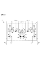
図2は、第1の実施の形態に係る撮像素子3の画素の構成を示す回路図である。画素10は、マイクロレンズMLと、第1の光電変換部11aと、第2の光電変換部11bと、第1の転送部12aと、第2の転送部12bと、第1のリセット部13aと、第2のリセット部13bと、第1の蓄積部14aと、第2の蓄積部14bとを有する。画素10は、さらに、第1の増幅部15aと、第2の増幅部15bと、第1の選択部16aと、第2の選択部16bと、加算スイッチ部17と、第1の接続スイッチ部19aと、第2の接続スイッチ部19bと、第1の領域20aと、第2の領域20bとを有する。
マイクロレンズMLは、図1の撮像光学系2を介して入射された光を第1の光電変換部11a及び第2の光電変換部11bに集光する。なお、マイクロレンズMLは、マイクロレンズMLを通過した光束が第1及び第2の光電変換部11a、11bに入射することを示すために、第1及び第2の光電変換部11a、11bを囲む楕円形状の線で示されている。この楕円形状がマイクロレンズMLの実際の大きさや、実際の形状を表すものではない。
第1の光電変換部11a及び第2の光電変換部11bは、フォトダイオードPD(PDa、PDb)であり、入射した光を電荷に変換し、光電変換された電荷を蓄積する機能を有する。第1の光電変換部11a及び第2の光電変換部11bは、一つのマイクロレンズMLに対応して配置され、撮像光学系2の射出瞳の互いに異なる領域を通過した光束を受光する。すなわち、第1の光電変換部11a及び第2の光電変換部11bは、撮像光学系2の射出瞳の第1及び第2の領域をそれぞれ通過した第1及び第2の光束による第1及び第2の像をそれぞれ光電変換する。
第1の転送部12aは、信号TX1により制御されるトランジスタM1aから構成される。第1の転送部12aは、第1の接続スイッチ部19aのトランジスタM9aがオフの場合は、第1の光電変換部11aで光電変換された電荷を第1の蓄積部14aに転送する。すなわち、第1の転送部12aは、第1の光電変換部11a及び第1の蓄積部14aの間に電荷転送路を形成する。なお、第1の接続スイッチ部19aのトランジスタM9aがオンの場合には、第1の転送部12aは、第1の光電変換部11aで光電変換された電荷を第1の蓄積部14a及び第1の領域20aに転送する。トランジスタM1aは、第1の転送トランジスタである。第1の蓄積部14aには、第1の蓄積部14aに接続される各トランジスタの容量(寄生容量)や配線容量等の容量が付加される。第1の蓄積部14aは、第1の蓄積部14aに転送された電荷を蓄積(保持)して、電荷を容量値で除算した電圧に変換する。
第1の接続スイッチ部19aは、信号ADD_FD1により制御されるトランジスタM9aにより構成され、第1の蓄積部14aと第1の増幅部15aとを接続(結合)する。また、第1の接続スイッチ部19aが、第1の蓄積部14aと第1の領域20aとを接続するともいえる。第1の領域20aには、第1の領域20aに接続される第1の増幅部15aのゲート容量等の各トランジスタの容量や配線容量の容量が付加される。第1の領域20aは、第1の領域20aに転送された電荷を蓄積して、容量値で除算した電圧に変換する。
第1の増幅部15aは、光電変換部から転送された電荷による信号を増幅して出力する。第1の増幅部15aは、トランジスタM3aにより構成される。トランジスタM3aのドレイン(端子)は、電源VDDに接続され、トランジスタM3aのゲート(端子)は、第1の接続スイッチ部19aのトランジスタM9aのドレインに接続される。また、トランジスタM3aのソース(端子)は、第1の選択部16aのトランジスタM4aに接続される。第1の増幅部15aのトランジスタM3aのソースは、第1の選択部16aを介して第1の垂直信号線VLaに接続される。第1の増幅部15aは、図3に示す第1の電流源25aを負荷電流源としてソースフォロワ回路の一部として機能する。トランジスタM3aは、第1の増幅トランジスタである。
第1のリセット部13aは、信号RS1により制御されるトランジスタM2aから構成され、第1の領域20aと第1の蓄積部14aの電荷をリセットし、第1の領域20aと第1の蓄積部14aの電圧をリセットする。トランジスタM2aは、第1のリセットトランジスタである。第1の選択部16aは、信号SEL1により制御されるトランジスタM4aから構成され、第1の増幅部15aからの信号を第1の垂直信号線VLaに出力する。トランジスタM4aは、第1の選択トランジスタである。本実施の形態による第1の出力部は、第1の増幅部15aと第1の選択部16aと第1のリセット部13aとで構成され、第1の光電変換部11aにより生成された電荷に基づく信号を生成し出力する。
第2の転送部12bは、信号TX2により制御されるトランジスタM1bから構成される。第2の転送部12bは、第2の接続スイッチ部19bのトランジスタM9bがオフの場合は、第2の光電変換部11bで光電変換された電荷を第2の蓄積部14bに転送する。すなわち、第2の転送部12bは、第2の光電変換部11b及び第2の蓄積部14bの間に電荷転送路を形成する。なお、第2の接続スイッチ部19bのトランジスタM9bがオンの場合には、第2の転送部12bは、第2の光電変換部11bで光電変換された電荷を第2の蓄積部14b及び第2の領域20bに転送する。トランジスタM1bは、第2の転送トランジスタである。第2の蓄積部14bには、第2の蓄積部14bに接続される各トランジスタの容量や配線容量等の容量が付加される。第2の蓄積部14bは、第2の蓄積部14bに転送された電荷を蓄積し、電荷を容量値で除算した電圧に変換する。
第2の接続スイッチ部19bは、信号ADD_FD2により制御されるトランジスタM9bにより構成され、第2の蓄積部14bと第2の増幅部15bとを接続する。また、第2の接続スイッチ部19bが、第2の蓄積部14bと第2の領域20bとを接続するともいえる。第2の領域20bには、第2の領域20bに接続される第2の増幅部15bのゲート容量等の各トランジスタの容量や配線容量の容量が付加される。第2の領域20bは、第2の領域20bに転送された電荷を蓄積して、容量値で除算した電圧に変換する。
第2の増幅部15bは、光電変換部から転送された電荷による信号を増幅して出力する。第2の増幅部15bは、トランジスタM3bにより構成される。トランジスタM3bのドレインは、電源VDDに接続され、トランジスタM3bのゲートは、第2の接続スイッチ部19bのトランジスタM9bのドレインに接続される。また、トランジスタM3bのソースは、第2の選択部16bのトランジスタM4bに接続される。第2の増幅部15bのソースは、第2の選択部16bを介して第2の垂直信号線VLbに接続される。第2の増幅部15bは、図3に示す第2の電流源25bを負荷電流源としてソースフォロワ回路の一部として機能する。トランジスタM3bは、第2の増幅トランジスタである。
第2のリセット部13bは、信号RS2により制御されるトランジスタM2bから構成され、第2の領域20bと第2の蓄積部14bの電荷をリセットし、第2の領域20bと第2の蓄積部14bの電圧をリセットする。トランジスタM2bは、第2のリセットトランジスタである。第2の選択部16bは、信号SEL2により制御されるトランジスタM4bから構成され、第2の増幅部15bからの信号を第2の垂直信号線VLbに出力する。トランジスタM4bは、第2の選択トランジスタである。本実施の形態による第2の出力部は、第2の増幅部15bと第2の選択部16bと第2のリセット部13bとで構成され、第2の光電変換部11bにより生成された電荷に基づく信号を生成し出力する。
加算スイッチ部17は、信号ADD_FD3により制御されるトランジスタM7から構成され、第1の蓄積部14aと第2の蓄積部14bとを接続する。また、加算スイッチ部17が、第1の転送部12aと第2の転送部12bとを接続するともいえる。
第1の制御モードでは、制御部4は、撮像素子3を制御して、加算スイッチ部17のトランジスタM7をオフ(状態)、第1の接続スイッチ部19aのトランジスタM9aをオン、第2の接続スイッチ部19bのトランジスタM9bをオンとする。第1の光電変換部11aで光電変換された電荷は、第1の蓄積部14a及び第1の領域20aに転送される。そして、第1の光電変換部11aから転送された電荷に応じた信号(第1の画素信号)が、第1の増幅部15a及び第1の選択部16aによって第1の垂直信号線VLaに読み出される。また、第2の光電変換部11bで光電変換された電荷は、第2の蓄積部14b及び第2の領域20bに転送される。第2の光電変換部11bから転送された電荷に応じた信号(第2の画素信号)が、第2の増幅部15b及び第2の選択部16bによって第2の垂直信号線VLbに読み出される。
このように、第1の制御モードでは、第1の光電変換部11aからの電荷に応じて生成された第1の画素信号が第1の垂直信号線VLaに出力され、第2の光電変換部11bからの電荷に応じて生成された第2の画素信号が第2の垂直信号線VLbに出力される。第1の画素信号及び第2の画素信号は、後述するカラム回路等による信号処理が施された後に、一対の焦点検出信号として制御部4に出力される。
次に、第2の制御モードの基本動作を説明する。第2の制御モードにおいては、制御部4は、加算スイッチ部17のトランジスタM7をオンとする。制御部4は、例えば、第1の接続スイッチ部19aのトランジスタM9aをオン、第2の接続スイッチ部19bのトランジスタM9bをオフ、第1の選択部16aのトランジスタM4aをオン、第2の選択部16bのトランジスタM4bをオフとする。第1及び第2の光電変換部11a、11bでそれぞれ光電変換された電荷は、第1及び第2の転送部12a、12bによってそれぞれ転送され、加算スイッチ部17によって加算される。第1の増幅部15aと第1の選択部16aとによって、加算された電荷に応じて加算画素信号が生成されて、第1の垂直信号線VLaに読み出される。なお、第1の接続スイッチ部19aのトランジスタM9aをオフ、第2の接続スイッチ部19bのトランジスタM9bをオン、第1の選択部16aのトランジスタM4aをオフ、第2の選択部16bのトランジスタM4bをオンとした場合には、加算画素信号は、第2の垂直信号線VLbに読み出される。
本実施の形態にあっては、第2の制御モードは、2次元配置された画素10の1行毎に信号を読み出す1行読み出し方式と、2行同時に信号を読み出す2行同時読み出し方式とを有する。以下では、第2の制御モードの「1行読み出し方式」を図3を用いて説明し、第2の制御モードの「2行同時読み出し方式」を図4を用いて説明する。
図3は、2次元状に配置された複数の画素10のうちの一つの画素列を示したものである。撮像素子3には、列方向、すなわち縦方向に並んだ複数の画素10の列に対して、第1の垂直信号線VLa及び第2の垂直信号線VLbが設けられる。また、第1の垂直信号線VLaに対して第1の電流源25a及び第1のカラム回路部40aが設けられ、第2の垂直信号線VLbに対して第2の電流源25b及び第2のカラム回路部40bが設けられる。なお、図3に示す例では、説明を簡略化するために、画素10は行方向1画素×列方向3画素のみ図示しているが、撮像素子3は、例えば数百万画素~数億画素、又はそれ以上の画素を有する。
第1の電流源25aは、第1の垂直信号線VLaを介して各画素10に接続され、第2の電流源25bは、第2の垂直信号線VLbを介して各画素10に接続される。第1の電流源25a及び第2の電流源25bは、各画素10から信号を読み出すための電流を生成する。第1の電流源25aは、生成した電流を第1の垂直信号線VLaと各画素10の第1の選択部16a及び第1の増幅部15aとに供給する。同様に、第2の電流源25bは、生成した電流を第2の垂直信号線VLbと各画素10の第2の選択部16b及び第2の増幅部15bとに供給する。
第1のカラム回路部40a及び第2のカラム回路部40bは、それぞれアナログ/デジタル変換部(AD変換部)を含んで構成される。第1のカラム回路部40aは、各画素10から第1の垂直信号線VLaを介して入力される信号をデジタル信号に変換する。第2のカラム回路部40bは、各画素10から第2の垂直信号線VLbを介して入力される信号をデジタル信号に変換する。第1のカラム回路部40a及び第2のカラム回路部40bは、変換後のデジタル信号を後述する水平転送部に出力する。
第2の制御モードの1行読み出し方式では、撮像素子3は、第1の光電変換部11aの電荷と第2の光電変換部11bの電荷とを加算した電荷に応じた信号(加算画素信号)を、例えば第1の垂直信号線VLaに読み出す。図3に示す例では、1行目の画素10、即ち最下行の画素10から加算画素信号を読み出す例を示している。1行目の画素10では、加算スイッチ部17のトランジスタM7がオン、第1の接続スイッチ部19aのトランジスタM9aがオン、第2の接続スイッチ部19bのトランジスタM9bがオフとなっている。また、1行目の画素10において、第1の選択部16aのトランジスタM4aがオン、第2の選択部16bのトランジスタM4bがオフになっている。他方、2行目及び3行目等のその他の行の画素10においては、第1及び第2の選択部16a、16bのトランジスタM4a、M4bがオフになっている。なお、図3において、ONはトランジスタがオン(接続状態、導通状態、短絡状態)であることを示し、OFFはトランジスタがオフ(切断状態、非導通状態、開放状態、遮断状態)であることを示している。
1行目の画素10において、加算スイッチ部17のトランジスタM7がオンとなり、第1の接続スイッチ部19aのトランジスタM9aがオンとなることで、第1の蓄積部14aと第2の蓄積部14bと第1の領域20aとが互いに電気的に接続される。また、第1の転送部12aと第2の転送部12bとが互いに電気的に接続される。第2の接続スイッチ部19bのトランジスタM9bはオフであるため、第1の蓄積部14a、第2の蓄積部14b、及び第1の領域20aに対して第2の領域20bが電気的に切り離される。これにより、第1の蓄積部14a、第2の蓄積部14b、及び第1の領域20aにおいて、第1の光電変換部11aから転送された電荷と第2の光電変換部11bから転送された電荷とが加算される。第1の光電変換部11a及び第2の光電変換部11bの各々により生成された電荷が、混合(合成)されるともいえる。
第1の蓄積部14a、第2の蓄積部14b、及び第1の領域20aの各々の容量が電気的に接続された状態となり、第1の光電変換部11a及び第2の光電変換部11bから転送された電荷がそれぞれの容量に分配される。第1の蓄積部14aの電圧と第2の蓄積部14bの電圧と第1の領域20aの電圧とが平均化され、第1の増幅部15aに入力される。即ち、第1の増幅部15aには、第1及び第2の蓄積部14a、14b、及び第1の領域20aの各々の蓄積電荷を加算した電荷を、第1及び第2の蓄積部14a、14b、及び第1の領域20aの各々の容量の合成容量値で除算した電圧が入力される。
1行目の画素10において、第1の選択部16aのトランジスタM4aがオンとなることで、第1の増幅部15aは、第1の電流源25aから電流が供給されて飽和領域での動作となる。第1の増幅部15aのトランジスタM3aが飽和領域での動作となるので、第1の増幅部15aのゲート容量は略一定の容量値となる。第1の増幅部15aのゲート容量が略一定値であるので、第1の蓄積部14aの容量、第2の蓄積部14bの容量、及び第1の領域20aの容量の合成容量も、所定値のままである。第1の増幅部15aは、第1及び第2の蓄積部14a、14b、及び第1の領域20aの各々の蓄積電荷を加算した電荷を合成容量値で除算した電圧に基づき、加算画素信号を生成する。加算画素信号は、第1の選択部16aを介して、第1の垂直信号線VLaに送られる。
以上のように、第1の垂直信号線VLaに1行目の画素10から加算画素信号が読み出されると、その後に、撮像素子3では、2行目、3行目と画素10が行単位で順次選択されて、画素10から第1の垂直信号線VLaに加算画素信号の読み出しが行われる。第1の垂直信号線VLaに出力された画素10の加算画素信号は、第1のカラム回路部40aによりデジタル信号に変換された後に、撮像信号として制御部4に出力される。
図3に示す例では、各行の画素10の加算画素信号は、第1の垂直信号線VLaに読み出される。このため、撮像素子3は、加算画素信号が読み出されない第2の垂直信号線VLbに接続される第2の電流源25bによる電流の生成を停止させることができ、撮像素子3の消費電力を低減させることができる。なお、第1の選択部16aのトランジスタM4aをオフ、第2の選択部16bのトランジスタM4bをオン、第1の接続スイッチ部19aのトランジスタM9aをオフ、第2の接続スイッチ部19bのトランジスタM9bをオンとした場合は、第2の垂直信号線VLbに画素10から加算画素信号を読み出すことができる。
本実施の形態にあっては、第1及び第2の蓄積部14a、14b及び第1の領域20aが電荷を電圧に変換する際の変換ゲインは、第1の蓄積部14aの容量、第2の蓄積部14bの容量、及び第1の領域20aの容量の合成容量値の逆数となる。このため、第1及び第2の蓄積部14a、14b、及び第1の領域20aに対して第2の領域20bが電気的に接続された場合と比較して、変換ゲインを大きくすることができる。この結果、S/N比を向上させて、ノイズの少ない加算画素信号を得ることができる。
また、本実施の形態にあっては、電荷を電圧に変換する際の変換ゲイン、即ち第1の蓄積部14aの容量、第2の蓄積部14bの容量、及び第1の領域20aの容量の合成容量値の逆数が、常に略一定である。このため、加算画素信号は、第1及び第2の蓄積部14a、14b及び第1の領域20aの蓄積電荷に依存し、直線性(リニアリティ)が高い信号となる。以下に、第1及び第2の蓄積部14a、14b及び第1の領域20aの変換ゲインが大きいこと、及び変換ゲインが常に略一定であることを、比較例と対比して説明する。
本実施の形態では、上述のように第2の接続スイッチ部19bのトランジスタM9bがオフとなることで、第2の領域20bが、第1及び第2の蓄積部14a、14b、及び第1の領域20aから電気的に切断される。このため、第1及び第2の光電変換部11a、11bから電荷が転送される領域の容量が小さくなる。すなわち、第1及び第2の光電変換部11a、11bにより生成された電荷は、第2の領域20bの容量には蓄積されずに、第1及び第2の蓄積部14a、14b、及び第1の領域20aの各々の容量に蓄積される。この結果、電荷電圧の変換ゲインを大きくすることができる。
また、本実施の形態では、第2の増幅部15bのトランジスタM3bのゲート容量が、第1及び第2の蓄積部14a、14b及び第1の領域20aから電気的に切り離される。このため、転送された電荷を電圧に変化する際の変換ゲインは、第1の蓄積部14aの容量、第2の蓄積部14bの容量、及び第1の領域20aの容量の合成容量値の逆数となり、トランジスタM3bのゲート容量の変動の影響を受けることなく、略一定値となる。
これに対して、比較例は、図3の画素10において、第1の接続スイッチ部19a及び第2の接続スイッチ部19bを削除したものである。この場合、第1の蓄積部14aと第2の蓄積部14bと第1の領域20aと第2の領域20bとが互いに電気的に接続される。第1の増幅部15aには、第1及び第2の蓄積部14a、14bと第1及び第2の領域20a、20bの蓄積電荷を加算した電荷を、第1及び第2の蓄積部14a、14bと第1及び第2の領域20a、20bの容量の合成容量値で除算した電圧が入力される。第1及び第2の蓄積部14a、14bと第1及び第2の領域20a、20bの変換ゲインは、第1の蓄積部14aの容量、第2の蓄積部14bの容量、第1の領域20aの容量、及び第2の領域20bの容量の合成容量値の逆数となる。このため、変換ゲインが低下し、S/N比が低下することとなる。
また、第1の選択部16aのトランジスタM4aをオンし、第2の選択部16bのトランジスタM4bをオフにすると、第1の増幅部15aには電流が供給されるが、第2の増幅部15bには電流が供給されず、第2の増幅部15bは弱反転領域での動作となる。この弱反転領域での動作により、第2の増幅部15bのゲート容量は、ゲートに入力される信号に応じて変動する状態となる。比較例では、第2の増幅部15bのゲート容量の変動によって、第1の増幅部15aに付加される合成容量も変動し、電荷電圧の変換ゲインが変動してしまう。
図4は、第2の制御モードの2行同時読み出し方式を説明するための図である。第2の制御モードの2行同時読み出し方式は、二つの行の画素について、一方の行の画素からは加算画素信号を第1の垂直信号線VLaに読み出し、これと同時に他方の行の画素からは加算画素信号を第2の垂直信号線VLbに読み出すものである。以下に詳細に説明する。
最下行の1行目の画素10では、加算スイッチ部17のトランジスタM7がオン、第1の接続スイッチ部19aのトランジスタM9aがオン、第2の接続スイッチ部19bのトランジスタM9bがオフとなっている。1行目の画素10では、さらに、第1の選択部16aのトランジスタM4aがオン、第2の選択部16bのトランジスタM4bがオフとなっている。また、2行目の画素10では、加算スイッチ部17のトランジスタM7がオン、第1の接続スイッチ部19aのトランジスタM9aがオフ、第2の接続スイッチ部19bのトランジスタM9bがオンとなっている。2行目の画素10では、さらに、第1の選択部16aのトランジスタM4aがオフ、第2の選択部16bのトランジスタM4bがオンとなっている。
1行目及び2行目の画素10の各々において、加算スイッチ部17のトランジスタM7がオン状態であるため、第1の光電変換部11aから転送された電荷と第2の光電変換部11bから転送された電荷とが加算される。また、1行目の画素10の各々において、第2の接続スイッチ部19bのトランジスタM9bのオフによって、第2の領域20bが、第2の蓄積部14bから電気的に切断される。他方、2行目の画素10の各々において、第1の接続スイッチ部19aのトランジスタM9aのオフによって、第1の領域20aが、第1の蓄積部14aから電気的に切断される。こうして、1行目及び2行目とも、電荷電圧の変換ゲインが大きくなると共に、変換ゲインは略一定値となる。
第1の垂直信号線VLaには、1行目の画素10から加算された電荷に基づく加算画素信号が読み出され、これと同時に第2の垂直信号線VLbには、2行目の画素10から加算された電荷に基づく加算画素信号が読み出される。1行目及び2行目の画素の同時読み出しが終了すると、3行目及び4行目の画素からの同時読み出しが行われ、更にそれ以降の互いに隣接する奇数行目及び偶数行目の画素からの同時読み出しが順次行われる。
このように、図4に示す2行同時読み出し方式では、2行分の画素の加算画素信号の読み出しを同時に行うことができる。このため、撮像素子3に配置された各画素10から高速に信号を読み出すことができる。
図5~図8を参照して、第1の実施の形態に係る撮像素子3のより詳細な回路構成及び動作について説明する。図5は、第1の実施の形態に係る撮像素子3の画素10を2次元状に示すと共に、より詳細な回路構成を示す回路図である。図6は、第1の制御モードの場合の撮像素子3の動作例を示すタイミングチャートである。図7は、第2の制御モードの1行読み出し方式の場合の撮像素子3の動作例を示すタイミングチャートである。図8は、第2の制御モードの2行同時読み出し方式の場合の撮像素子3の動作例を示すタイミングチャートである。
図5に示すように、撮像素子3は、行列状に配置される複数の画素10と、第1の電流源25a(第1の電流源25a1~第1の電流源25a3)と、第2の電流源25b(第2の電流源25b1~第2の電流源25b3)とを有する。また、撮像素子3は、第1の電流制御部30a(第1の電流制御部30a1~第1の電流制御部30a3)と、第2の電流制御部30b(第2の電流制御部30b1~第2の電流制御部30b3)とを有する。撮像素子3は、さらに、第1のカラム回路部40a(第1のカラム回路部40a1~第1のカラム回路部40a3)と、第2のカラム回路部40b(第2のカラム回路部40b1~第2のカラム回路部40b3)と、垂直駆動部50と、水平転送部60とを有する。
画素10の各列に対応して、第1の垂直信号線VLa(第1の垂直信号線VLa1~第1の垂直信号線VLa3)、及び第2の垂直信号線VLb(第2の垂直信号線VLb1~第2の垂直信号線VLb3)が設けられる。第1の垂直信号線VLaに対して、第1の電流源25a、第1の電流制御部30a、及び第1のカラム回路部40aが設けられる。また、第2の垂直信号線VLbに対して、第2の電流源25b、第2の電流制御部30b、及び第2のカラム回路部40bが設けられる。なお、図5に示す例では、説明を簡略化するために、画素10は行方向3画素×列方向3画素のみ図示している。
垂直駆動部50は、信号TX、信号RS、信号SEL1、信号SEL2、信号ADD_FD1、信号ADD_FD2、及び信号ADD_FD3を各画素10に供給して、各画素10を制御する。第1の電流制御部30aは、スイッチ部31a、32a、及びインバータ部33aを有し、第2の電流制御部30bは、スイッチ部31b、32b、及びインバータ部33bを有する。垂直駆動部50は、信号CS1_EN、信号CS2_EN、及び電圧Vclipを、第1の電流制御部30a及び第2の電流制御部30bに供給する。なお、図5に示す例では、第1の転送部12a及び第2の転送部12bは、同一の信号TXにより制御され、第1のリセット部13a及び第2のリセット部13bは、同一の信号RSにより制御される。
水平転送部60は、第1のカラム回路部40a及び第2のカラム回路部40bにより変換されたデジタル信号を、不図示の信号処理部に順次転送する。信号処理部は、水平転送部60から入力された信号に対して相関二重サンプリングや信号量を補正する処理等の信号処理を行い、カメラ1の制御部4に出力する。
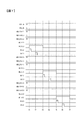
図6に示すタイミングチャートにおいて、横軸は時刻を示しており、第1の制御モードの場合に図5の撮像素子3の各部に入力される制御信号を示している。また、図6において、制御信号がハイレベル(例えば電源電位)の場合に制御信号が入力されるトランジスタがオン状態となり、制御信号がローレベル(例えば接地電位)の場合に制御信号が入力されるトランジスタがオフ状態となる。
垂直駆動部50は、信号ADD_FD1<2>~<0>をハイレベル、信号ADD_FD2<2>~<0>をハイレベル、及び信号ADD_FD3<2>~<0>をローレベルにして、第1の制御モードに設定する。信号ADD_FD1がハイレベルになることで、各画素10の第1の蓄積部14aと第1の増幅部15aとが互いに電気的に接続され、信号ADD_FD2がハイレベルになることで、各画素10の第2の蓄積部14bと第2の増幅部15bとが互いに電気的に接続される。また、信号ADD_FD3がローレベルになることで、各画素10の第1の蓄積部14aと第2の蓄積部14bとは電気的に切断される。
垂直駆動部50は、信号CS1_ENをハイレベルとし、信号CS2_ENもハイレベルとする。信号CS1_ENがハイレベルになることで、第1の電流制御部30aのスイッチ部31aがオンとなる。これにより、第1の垂直信号線VLaには、スイッチ部31aを介して第1の電流源25aから電流が供給される。また、信号CS2_ENがハイレベルになることで、第2の電流制御部30bのスイッチ部31bがオンとなる。これにより、第2の垂直信号線VLbには、スイッチ部31bを介して第2の電流源25bから電流が供給される。
図6に示す時刻t1では、信号RS<2>がハイレベルになることで、最上行の画素10において、それぞれの第1及び第2のリセット部13a、13bのトランジスタM2a、M2bがオンになる。第1の蓄積部14a、第2の蓄積部14b、第1の領域20a、及び第2の領域20bの電位がそれぞれリセット電位となる。
また、時刻t1において、信号SEL1<2>がハイレベルになることで、リセット電位に基づく信号が、第1の増幅部15a及び第1の選択部16aにより第1の垂直信号線VLaに出力される。すなわち、第1の蓄積部14a及び第1の領域20aの電位をリセット電位にリセットしたときの信号(第1のノイズ信号)が、第1の垂直信号線VLaに読み出される。第1の垂直信号線VLaに出力された各画素10からの第1のノイズ信号は、それぞれ第1のカラム回路部40a1~40a3に入力されてデジタル信号に変換される。また、時刻t1において、信号SEL2<2>がハイレベルになることで、第2の蓄積部14b及び第2の領域20bの電位をリセット電位にリセットしたときの信号(第2のノイズ信号)が、第2の増幅部15b及び第2の選択部16bにより第2の垂直信号線VLbに読み出される。第2の垂直信号線VLbに出力された各画素10からの第2のノイズ信号は、それぞれ第2のカラム回路部40b1~40b3に入力されてデジタル信号に変換される。
時刻t2では、信号TX<2>がハイレベルになることで、第1及び第2の転送部12a、12bのトランジスタM1a、M1bがオンになる。これにより、第1の光電変換部11aで光電変換された電荷が、第1の蓄積部14a及び第1の領域20aに転送される。また、第2の光電変換部11bで光電変換された電荷が、第2の蓄積部14b及び第2の領域20bに転送される。
また、時刻t2では、信号SEL1<2>がハイレベルであるため、第1の画素信号が、第1の増幅部15a及び第1の選択部16aにより第1の垂直信号線VLaに出力される。第1の垂直信号線VLaに出力された各画素10からの第1の画素信号は、それぞれ第1のカラム回路部40a1~40a3に入力されてデジタル信号に変換される。また、時刻t2では、信号SEL2<2>がハイレベルであるため、第2の画素信号が、第2の増幅部15b及び第2の選択部16bにより第2の垂直信号線VLbに出力される。第2の垂直信号線VLbに出力された各画素10からの第2の画素信号は、それぞれ第2のカラム回路部40b1~40b3に入力されてデジタル信号に変換される。デジタル信号に変換されたノイズ信号と画素信号とは、水平転送部60を介して信号処理部に入力される。信号処理部は、画素10のノイズ信号と加算画素信号との差分処理を行う相関二重サンプリングを行う。
時刻t3~時刻t5では、時刻t1から時刻t3までの期間の場合と同様にして、中央の行の画素からノイズ信号の読み出しと、画素信号の読み出しとが行われる。時刻t5~時刻t7では、時刻t1から時刻3までの期間の場合と同様にして、最下行の画素からノイズ信号の読み出しと、画素信号の読み出しとが行われる。このように、図6に示す第1の制御モードでは、第1の光電変換部11aで生成された電荷による信号を第1の垂直信号線VLaに読み出し、第2の光電変換部11bで生成された電荷による信号を第2の垂直信号線VLbに読み出すことができる。
図7に示すタイミングチャートにおいて、横軸は時刻を示しており、第2の制御モードの1行読み出し方式の場合に図5の撮像素子3の各部に入力される制御信号を示している。垂直駆動部50は、信号ADD_FD1<2>~<0>をハイレベル、信号ADD_FD2<2>~<0>をローレベル、及び信号ADD_FD3<2>~<0>をハイレベルにして、第2の制御モードに設定する。信号ADD_FD1がハイレベルになることで、各画素10の第1の蓄積部14aと第1の増幅部15aとが互いに電気的に接続され、信号ADD_FD2がローレベルになることで、各画素10の第2の蓄積部14bと第2の増幅部15bとが互いに電気的に切断される。また、信号ADD_FD3がハイレベルになることで、各画素10の第1の蓄積部14aと第2の蓄積部14bとが電気的に接続される。
垂直駆動部50は、信号CS1_ENをハイレベルとし、信号CS2_ENをローレベルとする。信号CS1_ENがハイレベルになることで、第1の垂直信号線VLaには、第1の電流源25aから電流が供給される。また、信号CS2_ENがローレベルになることで、第2の電流制御部30bのスイッチ部31bがオフとなり、スイッチ部32bはオンとなる。これにより、第2の垂直信号線VLbには、第2の電流源25bからの電流の供給が停止され、スイッチ部32bを介して電圧Vclipが供給される。第2の垂直信号線VLbは、所定の電圧に固定された状態となり、フローティング状態となることが回避される。
図7に示す時刻t1では、信号RS<2>がハイレベルになることで、最上行の画素10において、それぞれの第1及び第2のリセット部13a、13bのトランジスタM2a、M2bがオンになる。第1の蓄積部14a、第2の蓄積部14b、第1の領域20a、及び第2の領域20bの電位がそれぞれリセット電位となる。この場合、画素10の第1の蓄積部14aと第2の蓄積部14bと第1の領域20aが接続されているため、第1及び第2の蓄積部14a、14b、及び第1の領域20aの電位が平均化される。
また、時刻t1において、信号SEL1<2>がハイレベルになることで、リセット電位に基づく信号が、第1の増幅部15a及び第1の選択部16aにより第1の垂直信号線VLaに出力される。すなわち、第1及び第2の蓄積部14a、14b、及び第1の領域20aの電位をリセット電位にリセットしたときのノイズ信号が、第1の垂直信号線VLaに読み出される。第1の垂直信号線VLaに出力された各画素10からのノイズ信号は、それぞれ第1のカラム回路部40a1~40a3に入力されてデジタル信号に変換される。
時刻t2では、信号TX<2>がハイレベルになることで、第1及び第2の転送部12a、12bのトランジスタM1a、M1bがオンになる。これにより、第1及び第2の光電変換部11a、11bで光電変換された電荷が、第1及び第2の蓄積部14a、14b、及び第1の領域20aに転送される。
また、時刻t2では、信号SEL1<2>がハイレベルであるため、加算画素信号が、第1の増幅部15a及び第1の選択部16aにより第1の垂直信号線VLaに出力される。第1の垂直信号線VLaに出力された各画素10からの加算画素信号は、それぞれ第1のカラム回路部40a1~40a3に入力されてデジタル信号に変換される。デジタル信号に変換されたノイズ信号と加算画素信号とは、水平転送部60を介して信号処理部に入力される。信号処理部は、画素10のノイズ信号と加算画素信号との差分処理を行う相関二重サンプリングを行う。
時刻t3~時刻t5では、時刻t1から時刻t3までの期間の場合と同様にして、中央の行の画素からノイズ信号の読み出しと、加算画素信号の読み出しとが行われる。時刻t5~時刻t7では、時刻t1から時刻3までの期間の場合と同様にして、最下行の画素からノイズ信号の読み出しと、加算画素信号の読み出しとが行われる。このように、図7に示す1行読み出し方式では、画素10を行単位で順次選択し、画素10の2つの光電変換部による信号を加算し、加算画素信号を第1の垂直信号線VLaに読み出すことができる。また、第2の電流源25bからの電流の供給を停止することで、撮像素子3の消費電力を低減することができる。
図8に示すタイミングチャートにおいて、横軸は時刻を示しており、第2の制御モードの2行同時読み出し方式の場合に図5の撮像素子3の各部に入力される制御信号を示している。垂直駆動部50は、信号ADD_FD1<2>、<0>をハイレベル、信号ADD_FD1<1>をローレベルにする。また、垂直駆動部50は、信号ADD_FD2<2>、<0>をローレベル、信号ADD_FD2<1>をハイレベルにする。さらに、垂直駆動部50は、信号ADD_FD3<2>~<0>をハイレベルにする。信号ADD_FD3がハイレベルになることで、各画素10の第1の蓄積部14aと第2の蓄積部14bとが電気的に接続される。
最上行及び最下行の各画素10では、信号ADD_FD1<2>、<0>がハイレベルになることで、第1の蓄積部14aと第1の増幅部15aとが互いに電気的に接続される。また、信号ADD_FD2<2>、<0>がローレベルになることで、第2の蓄積部14bと第2の増幅部15bとが互いに電気的に切断される。
中央行の各画素10では、信号ADD_FD1<1>がローレベルになることで、第1の蓄積部14aと第1の増幅部15aとが互いに電気的に切断される。また、信号ADD_FD2<1>がハイレベルになることで、第2の蓄積部14bと第2の増幅部15bとが互いに電気的に接続される。
垂直駆動部50は、信号CS1_ENをハイレベルとし、信号CS2_ENもハイレベルとする。これにより、第1の垂直信号線VLaには、第1の電流源25aから電流が供給され、第2の垂直信号線VLbには、第2の電流源25bから電流が供給される。
図8に示す時刻t1では、信号RS<2>がハイレベルになることで、最上行の画素10において、それぞれの第1及び第2のリセット部13a、13bのトランジスタM2a、M2bがオンになる。第1の蓄積部14a、第2の蓄積部14b、第1の領域20a、及び第2の領域20bの電位がそれぞれリセット電位となる。この場合、画素10の第1の蓄積部14aと第2の蓄積部14bと第1の領域20aが接続されているため、第1及び第2の蓄積部14a、14b、及び第1の領域20aの電位が平均化される。
また、時刻t1において、信号SEL1<2>がハイレベルになることで、最上行の画素10のリセット電位に基づく信号が、第1の増幅部15a及び第1の選択部16aにより第1の垂直信号線VLaに出力される。すなわち、第1及び第2の蓄積部14a、14b、及び第1の領域20aの電位をリセット電位にリセットしたときのノイズ信号が、第1の垂直信号線VLaに読み出される。第1の垂直信号線VLaに出力された最上行の各画素10からのノイズ信号は、それぞれ第1のカラム回路部40a1~40a3に入力されてデジタル信号に変換される。
また、時刻t1では、信号RS<1>がハイレベルになることで、中央行の画素10において、それぞれの第1及び第2のリセット部13a、13bのトランジスタM2a、M2bがオンになる。第1の蓄積部14a、第2の蓄積部14b、第1の領域20a、及び第2の領域20bの電位がそれぞれリセット電位となる。この場合、画素10の第1の蓄積部14aと第2の蓄積部14bと第2の領域20bが接続されているため、第1及び第2の蓄積部14a、14b、及び第2の領域20bの電位が平均化される。
また、時刻t1において、信号SEL2<1>がハイレベルになることで、中央行の画素10のリセット電位に基づく信号が、第2の増幅部15b及び第2の選択部16bにより第2の垂直信号線VLbに出力される。すなわち、第1及び第2の蓄積部14a、14b、及び第2の領域20bの電位をリセット電位にリセットしたときのノイズ信号が、第2の垂直信号線VLbに読み出される。第2の垂直信号線VLbに出力された中央行の各画素10からのノイズ信号は、それぞれ第2のカラム回路部40b1~40b3に入力されてデジタル信号に変換される。
時刻t2では、信号TX<2>がハイレベルになることで、最上行の画素10において、第1及び第2の転送部12a、12bのトランジスタM1a、M1bがオンになる。これにより、第1及び第2の光電変換部11a、11bで光電変換された電荷が、第1及び第2の蓄積部14a、14b、及び第1の領域20aに転送される。
また、時刻t2では、信号SEL1<2>がハイレベルであるため、最上行の画素10の加算画素信号が、第1の増幅部15a及び第1の選択部16aにより第1の垂直信号線VLaに出力される。第1の垂直信号線VLaに出力された最上行の各画素10からの加算画素信号は、それぞれ第1のカラム回路部40a1~40a3に入力されてデジタル信号に変換される。
時刻t2では、信号TX<1>がハイレベルになることで、中央行の画素10において、第1及び第2の転送部12a、12bのトランジスタM1a、M1bがオンになる。これにより、第1及び第2の光電変換部11a、11bで光電変換された電荷が、第1及び第2の蓄積部14a、14b、及び第2の領域20bに転送される。
また、時刻t2では、信号SEL2<1>がハイレベルであるため、中央行の画素10の加算画素信号が、第2の増幅部15b及び第2の選択部16bにより第2の垂直信号線VLbに出力される。第2の垂直信号線VLbに出力された中央行の各画素10からの加算画素信号は、それぞれ第2のカラム回路部40b1~40b3に入力されてデジタル信号に変換される。デジタル信号に変換されたノイズ信号と加算画素信号とは、水平転送部60を介して信号処理部に入力される。信号処理部は、画素10のノイズ信号と加算画素信号との差分処理を行う相関二重サンプリングを行う。
時刻t3以降の期間では、時刻t1から時刻t3までの期間の場合と同様にして、互いに隣接する奇数行目及び偶数行目の画素からの同時読み出しが順次行われる。このように、図8に示す2行同時読み出し方式は、2行分の画素の信号の読み出しを同時に行うことができる。このため、撮像素子3に配置された各画素10から高速に信号を読み出すことができる。
次に、第1の制御モードと、第2の制御モードの1行読み出し方式と、第2の制御モードの2行同時読み出し方式との使い分けについて、説明する。制御部4は、カメラ1が焦点調節動作を行う場合には、撮像素子3を第1の制御モードで制御する。また、制御部4は、カメラ1が、表示部6に被写体のスルー画像(ライブビュー画像)を表示する場合には、撮像素子3を第2の制御モードの1行読み出し方式又は2行同時読み出し方式で制御する。従って、カメラ1が表示部6に被写体のスルー画像(ライブビュー画像)を表示しながら、焦点調節動作を行う場合には、制御部4は、撮像素子3を時分割的に、第2の制御モードの1行読み出し方式又は2行同時読み出し方式で制御すると共に第1の制御モードで制御する。操作部7のレリーズ操作部材が操作された場合には、制御部4は、撮像素子3を第2の制御モードの1行読み出し方式又は2行同時読み出し方式で制御する。
更に、カメラ1がフレームレートの高い撮影、例えば高速連写撮影や動画撮影を行う場合には、制御部4は、加算画素信号の高速読み出しの為に撮像素子3を第2の制御モードの2行同時読み出し方式で制御する。また、カメラ1に設けられた被写体移動速度検出部が被写体が比較的高速で移動していることを検出した場合にも、制御部4は、加算画素信号を高速に読み出して画像のブレを少なくするために、撮像素子3を第2の制御モードの2行同時読み出し方式で制御する。他方、カメラ1の駆動電池の残量が少なくなったことを、電池残量検出部が検出した場合には、制御部4は電池の消費を少なくするために、撮像素子3を第2の制御モードの1行読み出し方式で制御する。
上述した実施の形態によれば、次の作用効果が得られる。
(1)撮像素子3は、入射光を光電変換して第1電荷を生成する第1の光電変換部11aと、入射光を光電変換して第2電荷を生成する第2の光電変換部11bと、第1の光電変換部11aで生成された第1電荷を蓄積する第1の蓄積部14aと、第2の光電変換部11bで生成された第2電荷を蓄積する第2の蓄積部14bと、第1の蓄積部14aと第2の蓄積部14bとを接続切断する第1のスイッチ(加算スイッチ部17)と、第1の蓄積部14aと接続される第1の出力部(第1の増幅部15a及び第1の選択部16a)と、第2の蓄積部14bと第2の接続部(第2の接続スイッチ部19b)を介して接続切断される第2の出力部(第2の増幅部15b及び第2の選択部16b)と、を有する画素10を備える。本実施の形態では、第2の接続スイッチ部19bのトランジスタM9bをオフとすることで、第2の領域20bが、第1及び第2の蓄積部14a、14b、第1の領域20a、及び第1の増幅部15aから電気的に切断される。このため、電荷電圧の変換ゲインを大きくすることができる。この結果、S/N比を向上させて、ノイズの少ない加算画素信号を得ることができる。
(1)撮像素子3は、入射光を光電変換して第1電荷を生成する第1の光電変換部11aと、入射光を光電変換して第2電荷を生成する第2の光電変換部11bと、第1の光電変換部11aで生成された第1電荷を蓄積する第1の蓄積部14aと、第2の光電変換部11bで生成された第2電荷を蓄積する第2の蓄積部14bと、第1の蓄積部14aと第2の蓄積部14bとを接続切断する第1のスイッチ(加算スイッチ部17)と、第1の蓄積部14aと接続される第1の出力部(第1の増幅部15a及び第1の選択部16a)と、第2の蓄積部14bと第2の接続部(第2の接続スイッチ部19b)を介して接続切断される第2の出力部(第2の増幅部15b及び第2の選択部16b)と、を有する画素10を備える。本実施の形態では、第2の接続スイッチ部19bのトランジスタM9bをオフとすることで、第2の領域20bが、第1及び第2の蓄積部14a、14b、第1の領域20a、及び第1の増幅部15aから電気的に切断される。このため、電荷電圧の変換ゲインを大きくすることができる。この結果、S/N比を向上させて、ノイズの少ない加算画素信号を得ることができる。
(2)本実施の形態では、第2の接続スイッチ部19bのトランジスタM9bをオフとすることで、第1の増幅部15aが第2の増幅部15bのトランジスタM3bのゲート容量から電気的に切り離される。このため、トランジスタM3bのゲート容量の変動の影響を受けて変換ゲインが変動することを防ぐことができる。この結果、直線性が高い加算画素信号を得ることができる。
次のような変形も本発明の範囲内であり、変形例の一つ、もしくは複数を上述の実施形態と組み合わせることも可能である。
(変形例1)
上述した実施の形態では、画素10に第1の接続スイッチ部19a及び第2の接続スイッチ部19bが設けられる例について説明した。しかし、画素の構成を、第1の接続スイッチ部19a及び第2の接続スイッチ部19bのいずれか一方のみを有する構成としてもよい。図9に示すように、撮像素子3に、第1の接続スイッチ部19aを有する画素10Aと、第2の接続スイッチ部19bを有する画素10Bとを配置するようにしてもよい。
上述した実施の形態では、画素10に第1の接続スイッチ部19a及び第2の接続スイッチ部19bが設けられる例について説明した。しかし、画素の構成を、第1の接続スイッチ部19a及び第2の接続スイッチ部19bのいずれか一方のみを有する構成としてもよい。図9に示すように、撮像素子3に、第1の接続スイッチ部19aを有する画素10Aと、第2の接続スイッチ部19bを有する画素10Bとを配置するようにしてもよい。
画素10Aの第1の接続スイッチ部19aのトランジスタM9aがオフとなることで、第1の領域20aが、第1及び第2の蓄積部14a、14b、及び第2の領域20bから電気的に切断される。このため、第1及び第2の蓄積部14a、14b及び第2の領域20bの変換ゲインを大きくすることができる。他方、画素10Bの第2の接続スイッチ部19bのトランジスタM9bがオフとなることで、第2の領域20bが、第1及び第2の蓄積部14a、14b、及び第1の領域20aから電気的に切断される。このため、第1及び第2の蓄積部14a、14b及び第1の領域20aの変換ゲインを大きくすることができる。図9に示す例では、例えば、二つの行の画素について、一方の行の画素10Aからは加算画素信号を第2の垂直信号線VLbに読み出し、これと同時に他方の行の画素10Bからは加算画素信号を第1の垂直信号線VLaに読み出すことができる。
(変形例2)
上述した実施の形態では、画素10毎に複数の光電変換部が配置される例について説明した。しかし、画素10の構成を、一つの光電変換部を有する構成としてもよい。この場合、例えば図10に示すように、画素10には、加算スイッチ部17と接続スイッチ部19とが設けられる。加算スイッチ部17は、例えば行方向にそれぞれ配置される複数の画素10の各々の蓄積部14を接続する。接続スイッチ部19は、蓄積部14と増幅部15とを接続する。制御部4は、接続スイッチ部19をオンオフ制御することで、画素10の蓄積部14と増幅部15とを切り離すことができ、電荷電圧の変換ゲインを大きくすることができる。なお、接続スイッチ部19は、画素10毎に配置されなくてもよい。撮像素子3において、接続スイッチ部19を有する画素と接続スイッチ部19を有しない画素とを配置するようにしてもよい。例えば、撮像素子3において、接続スイッチ部19を有する画素と有しない画素とを交互に配置してもよい。また、加算スイッチ部17は、画素10毎に配置されなくてもよい。加算スイッチ部17を、複数の画素毎に配置して、複数の画素で共有する構成としてもよい。
上述した実施の形態では、画素10毎に複数の光電変換部が配置される例について説明した。しかし、画素10の構成を、一つの光電変換部を有する構成としてもよい。この場合、例えば図10に示すように、画素10には、加算スイッチ部17と接続スイッチ部19とが設けられる。加算スイッチ部17は、例えば行方向にそれぞれ配置される複数の画素10の各々の蓄積部14を接続する。接続スイッチ部19は、蓄積部14と増幅部15とを接続する。制御部4は、接続スイッチ部19をオンオフ制御することで、画素10の蓄積部14と増幅部15とを切り離すことができ、電荷電圧の変換ゲインを大きくすることができる。なお、接続スイッチ部19は、画素10毎に配置されなくてもよい。撮像素子3において、接続スイッチ部19を有する画素と接続スイッチ部19を有しない画素とを配置するようにしてもよい。例えば、撮像素子3において、接続スイッチ部19を有する画素と有しない画素とを交互に配置してもよい。また、加算スイッチ部17は、画素10毎に配置されなくてもよい。加算スイッチ部17を、複数の画素毎に配置して、複数の画素で共有する構成としてもよい。
(変形例3)
上述した実施の形態では、1画素に2つの光電変換部を配置する例について説明したが、画素の構成はこれに限らない。画素の構成を、1画素あたり3つ以上の光電変換部を有する構成にしてもよい。この場合には、例えば、第1の制御モードでは複数の光電変換部からの信号を個別に読み出し、第2の制御モードでは複数の光電変換部のうち2つ以上の光電変換部からの信号を加算して読み出すようにしてもよい。
上述した実施の形態では、1画素に2つの光電変換部を配置する例について説明したが、画素の構成はこれに限らない。画素の構成を、1画素あたり3つ以上の光電変換部を有する構成にしてもよい。この場合には、例えば、第1の制御モードでは複数の光電変換部からの信号を個別に読み出し、第2の制御モードでは複数の光電変換部のうち2つ以上の光電変換部からの信号を加算して読み出すようにしてもよい。
(変形例4)
上述した実施の形態および変形例では、光電変換部としてフォトダイオードを用いる例について説明した。しかし、光電変換部として光電変換膜を用いるようにしてもよい。
上述した実施の形態および変形例では、光電変換部としてフォトダイオードを用いる例について説明した。しかし、光電変換部として光電変換膜を用いるようにしてもよい。
(変形例5)
上述の実施の形態および変形例で説明した撮像素子3は、カメラ、スマートフォン、タブレット、PCに内蔵のカメラ、車載カメラ、無人航空機(ドローン、ラジコン機等)に搭載されるカメラ等に適用されてもよい。
上述の実施の形態および変形例で説明した撮像素子3は、カメラ、スマートフォン、タブレット、PCに内蔵のカメラ、車載カメラ、無人航空機(ドローン、ラジコン機等)に搭載されるカメラ等に適用されてもよい。
上記では、種々の実施の形態および変形例を説明したが、本発明はこれらの内容に限定されるものではない。本発明の技術的思想の範囲内で考えられるその他の態様も本発明の範囲内に含まれる。
次の優先権基礎出願の開示内容は引用文としてここに組み込まれる。
日本国特許出願2017年第16286号(2017年1月31日出願)
日本国特許出願2017年第16286号(2017年1月31日出願)
3 撮像素子、4 制御部、10 画素、11a 第1の光電変換部、11b 第2の光電変換部、17 加算スイッチ部、19a 第1の接続スイッチ部、19b 第2の接続スイッチ部、50 垂直駆動部
Claims (14)
- 光を光電変換して電荷を生成する第1の光電変換部と、前記第1の光電変換部で生成された電荷を蓄積する第1の蓄積部と、前記第1の蓄積部と接続される第1の出力部と、を有する第1画素と、
光を光電変換して電荷を生成する第2の光電変換部と、前記第2の光電変換部で生成された電荷を蓄積する第2の蓄積部と、前記第2の蓄積部と第2の接続部を介して接続切断される第2の出力部と、を有する第2画素と、
前記第1の光電変換部および前記第2の光電変換部で生成された電荷に基づく信号が前記第1の出力部から出力されるとき前記第1の蓄積部および前記第2の蓄積部の容量を調整する調整部と、を備える撮像素子。 - 請求項1に記載の撮像素子において、
前記調整部は、前記第1の光電変換部で生成された電荷に基づく信号が前記第1の出力部から出力されるときの前記第1の蓄積部の容量と、前記第1の光電変換部および前記第2の光電変換部で生成された電荷に基づく信号が前記第1の出力部から出力されるときの前記第1の蓄積部および前記第2の蓄積部の容量とが同じになるよう前記第1の蓄積部および前記第2の蓄積部の容量を調整する撮像素子。 - 請求項1または請求項2に記載の撮像素子において、
前記第2の出力部と前記第2の蓄積部とは第2の接続部により接続され、前記調整部は、第2の接続部により前記第1の蓄積部および前記第2の蓄積部の容量を調整する撮像素子。 - 請求項3に記載の撮像素子において、
前記第1の光電変換部および前記第2の光電変換部で生成された電荷に基づく信号が前記第1の出力部から出力されるとき、前記第2の接続部は前記第2の出力部と前記第2の蓄積部とを切断する撮像素子。 - 光を光電変換して電荷を生成する第1の光電変換部と、前記第1の光電変換部で生成された電荷を蓄積する第1の蓄積部と、前記第1の蓄積部と第1の接続部を介して接続される第1の出力部と、を有する第1画素と、
光を光電変換して電荷を生成する第2の光電変換部と、前記第2の光電変換部で生成された電荷を蓄積する第2の蓄積部と、前記第2の蓄積部と第2の接続部を介して接続切断される第2の出力部と、を有する第2画素と、
を備える撮像素子。 - 請求項5に記載の撮像素子において、
前記第1の出力部と接続され、前記第1の出力部から信号が出力される第1の信号線と、
前記第2の出力部と接続され、前記第2の出力部から信号が出力される第2の信号線と、を備える撮像素子。 - 請求項6に記載の撮像素子において、
前記第1の光電変換部により生成された電荷に基づく信号と前記第2の光電変換部により生成された電荷に基づく信号とが前記第1の出力部から前記第1の信号線に出力されるとき、前記第2の接続部は前記第2の蓄積部と前記第2の出力部とを切断する撮像素子。 - 請求項6または請求項7に記載の撮像素子において、
前記第1の蓄積部に蓄積された電荷に基づく信号と前記第2の蓄積部に蓄積された電荷に基づく信号とが前記第1の出力部から前記第1の信号線に出力されるとき、前記第2の接続部は前記第2の蓄積部と前記第2の出力部とを切断する撮像素子。 - 請求項6から請求項8までのいずれか一項に記載の撮像素子において、
前記第1の光電変換部により生成された電荷に基づく信号と前記第2の光電変換部により生成された電荷に基づく信号とが前記第1の出力部から前記第1の信号線に出力されるとき、前記第1の接続部は前記第1の蓄積部と前記第1の出力部とを接続する撮像素子。 - 請求項6から請求項9までのいずれか一項に記載の撮像素子において、
前記第1の蓄積部に蓄積された電荷に基づく信号と前記第2の蓄積部に蓄積された電荷に基づく信号とが前記第1の出力部から前記第1の信号線に出力されるとき、前記第1の接続部は前記第1の蓄積部と前記第1の出力部とを接続する撮像素子。 - 請求項6から請求項10までのいずれか一項に記載の撮像素子において、
前記第1の蓄積部と前記第2の蓄積部とを接続する第3の接続部を備え、
前記第1の蓄積部と前記第2の蓄積部とが前記第3の接続部により接続されるとき、前記第1の蓄積部に蓄積された電荷に基づく信号と前記第2の蓄積部に蓄積された電荷に基づく信号とは前記第1の出力部から前記第1の信号線に出力される撮像素子。 - 請求項11に記載の撮像素子において、
前記第1の蓄積部と前記第2の蓄積部とが前記第3の接続部により切断されるとき、前記第1の蓄積部に蓄積された電荷に基づく信号は前記第1の出力部から前記第1の信号線に出力され、前記第2の蓄積部に蓄積された電荷に基づく信号は前記第2の出力部から前記第2の信号線に出力される撮像素子。 - 請求項7から請求項12までのいずれか一項に記載の撮像素子において、
前記第1画素は、前記第1の光電変換部で生成された電荷を前記第1の蓄積部に転送する第1の転送トランジスタを有し、
前記第2画素は、前記第2の光電変換部で生成された電荷を前記第2の蓄積部に転送する第2の転送トランジスタを有し、
前記第1の蓄積部は、前記第1の転送トランジスタのドレインであり、
前記第2の蓄積部は、前記第2の転送トランジスタのドレインであり、
前記第1の出力部は、前記第1の光電変換部で生成された電荷に基づいた信号を出力する第1の増幅トランジスタであり、
前記第2の出力部は、前記第2の光電変換部で生成された電荷に基づいた信号を出力する第2の増幅トランジスタであり、
前記第1の接続部は、前記第1の蓄積部と前記第1の増幅トランジスタとを接続し、
前記第2の接続部は、前記第2の蓄積部と前記第2の増幅トランジスタとを接続し、
前記第1の光電変換部により生成された電荷に基づく信号と前記第2の光電変換部により生成された電荷に基づく信号とが前記第1の出力部から前記第1の信号線に出力されるとき、前記第1の光電変換部で生成された電荷と前記第2の光電変換部で生成された電荷とは、前記第1の蓄積部及び前記第2の蓄積部及び前記第1の増幅トランジスタのゲートに蓄積される撮像素子。 - 請求項1から請求項13までのいずれか一項に記載の撮像素子と、
前記撮像素子から出力される信号に基づいて画像データを生成する画像生成部と、
を備える撮像装置。
Priority Applications (5)
| Application Number | Priority Date | Filing Date | Title |
|---|---|---|---|
| CN201880009220.7A CN110393007B (zh) | 2017-01-31 | 2018-01-31 | 摄像元件以及摄像装置 |
| JP2018565620A JP6809542B2 (ja) | 2017-01-31 | 2018-01-31 | 撮像素子および撮像装置 |
| US16/475,261 US11108978B2 (en) | 2017-01-31 | 2018-01-31 | Image sensor and image-capturing device including adjustment unit for reducing capacitance |
| US17/381,444 US11917310B2 (en) | 2017-01-31 | 2021-07-21 | Image sensor and image-capturing device including adjustment unit for reducing capacitance |
| US18/416,392 US20240155258A1 (en) | 2017-01-31 | 2024-01-18 | Image sensor and image-capturing device including adjustment unit for reducing capacitance |
Applications Claiming Priority (2)
| Application Number | Priority Date | Filing Date | Title |
|---|---|---|---|
| JP2017-016286 | 2017-01-31 | ||
| JP2017016286 | 2017-01-31 |
Related Child Applications (2)
| Application Number | Title | Priority Date | Filing Date |
|---|---|---|---|
| US16/475,261 A-371-Of-International US11108978B2 (en) | 2017-01-31 | 2018-01-31 | Image sensor and image-capturing device including adjustment unit for reducing capacitance |
| US17/381,444 Continuation US11917310B2 (en) | 2017-01-31 | 2021-07-21 | Image sensor and image-capturing device including adjustment unit for reducing capacitance |
Publications (1)
| Publication Number | Publication Date |
|---|---|
| WO2018143295A1 true WO2018143295A1 (ja) | 2018-08-09 |
Family
ID=63039799
Family Applications (1)
| Application Number | Title | Priority Date | Filing Date |
|---|---|---|---|
| PCT/JP2018/003278 WO2018143295A1 (ja) | 2017-01-31 | 2018-01-31 | 撮像素子および撮像装置 |
Country Status (4)
| Country | Link |
|---|---|
| US (3) | US11108978B2 (ja) |
| JP (3) | JP6809542B2 (ja) |
| CN (2) | CN113923383A (ja) |
| WO (1) | WO2018143295A1 (ja) |
Citations (4)
| Publication number | Priority date | Publication date | Assignee | Title |
|---|---|---|---|---|
| JP2015204469A (ja) * | 2014-04-10 | 2015-11-16 | キヤノン株式会社 | 撮像素子及び撮像装置 |
| JP2015211257A (ja) * | 2014-04-24 | 2015-11-24 | 株式会社東芝 | 固体撮像装置 |
| JP2016015680A (ja) * | 2014-07-03 | 2016-01-28 | 株式会社ニコン | 固体撮像素子および撮像装置 |
| JP2016139859A (ja) * | 2015-01-26 | 2016-08-04 | キヤノン株式会社 | 撮像装置及びその制御方法、プログラム、記憶媒体 |
Family Cites Families (29)
| Publication number | Priority date | Publication date | Assignee | Title |
|---|---|---|---|---|
| US7199410B2 (en) * | 1999-12-14 | 2007-04-03 | Cypress Semiconductor Corporation (Belgium) Bvba | Pixel structure with improved charge transfer |
| EP1102323B1 (en) | 1999-11-19 | 2012-08-15 | CSEM Centre Suisse d'Electronique et de Microtechnique SA - Recherche et Développement | Method for detecting electromagnetic radiation using an optoelectronic sensor |
| US6914227B2 (en) | 2001-06-25 | 2005-07-05 | Canon Kabushiki Kaisha | Image sensing apparatus capable of outputting image by converting resolution by adding and reading out a plurality of pixels, its control method, and image sensing system |
| JP4355148B2 (ja) * | 2003-02-28 | 2009-10-28 | パナソニック株式会社 | 固体撮像装置の駆動方法 |
| JP4049010B2 (ja) * | 2003-04-30 | 2008-02-20 | ソニー株式会社 | 表示装置 |
| JP4336544B2 (ja) * | 2003-07-18 | 2009-09-30 | パナソニック株式会社 | 固体撮像装置 |
| US7773143B2 (en) * | 2004-04-08 | 2010-08-10 | Tessera North America, Inc. | Thin color camera having sub-pixel resolution |
| US7719008B2 (en) * | 2006-02-03 | 2010-05-18 | Samsung Electronics Co., | Thin film transistor substrate and method of manufacturing the same and mask for manufacturing thin film transistor substrate |
| JP4416753B2 (ja) * | 2006-03-31 | 2010-02-17 | キヤノン株式会社 | 固体撮像装置 |
| JP2009177749A (ja) * | 2008-01-28 | 2009-08-06 | Panasonic Corp | 固体撮像装置 |
| JP5407264B2 (ja) * | 2008-10-09 | 2014-02-05 | ソニー株式会社 | 固体撮像素子およびカメラシステム |
| US8130302B2 (en) | 2008-11-07 | 2012-03-06 | Aptina Imaging Corporation | Methods and apparatus providing selective binning of pixel circuits |
| US8913166B2 (en) | 2009-01-21 | 2014-12-16 | Canon Kabushiki Kaisha | Solid-state imaging apparatus |
| ATE543215T1 (de) | 2009-03-24 | 2012-02-15 | Sony Corp | Festkörper-abbildungsvorrichtung, ansteuerverfahren für festkörper- abbildungsvorrichtung und elektronische vorrichtung |
| JP4941490B2 (ja) | 2009-03-24 | 2012-05-30 | ソニー株式会社 | 固体撮像装置、及び電子機器 |
| JP2011044887A (ja) | 2009-08-20 | 2011-03-03 | Canon Inc | 固体撮像装置 |
| GB2474014B (en) | 2009-09-24 | 2015-04-15 | Selex Es Ltd | IR detection system and method |
| JP5744599B2 (ja) | 2011-03-31 | 2015-07-08 | キヤノン株式会社 | 撮像素子、および撮像装置 |
| JP5926529B2 (ja) | 2011-10-18 | 2016-05-25 | キヤノン株式会社 | 撮像素子及び撮像装置 |
| FR2984608A1 (fr) | 2011-12-19 | 2013-06-21 | St Microelectronics Sa | Procede de capture d'image au moyen d'un capteur d'image |
| JP2014175934A (ja) | 2013-03-11 | 2014-09-22 | Canon Inc | 撮像素子、その駆動方法および撮像装置 |
| JP6346479B2 (ja) | 2013-05-16 | 2018-06-20 | キヤノン株式会社 | 撮像装置、撮像装置の制御方法及びプログラム |
| KR102211899B1 (ko) | 2013-11-18 | 2021-02-03 | 가부시키가이샤 니콘 | 고체 촬상 소자 및 촬상 장치 |
| US9674470B2 (en) | 2014-04-11 | 2017-06-06 | Semiconductor Energy Laboratory Co., Ltd. | Semiconductor device, method for driving semiconductor device, and method for driving electronic device |
| JP2016082306A (ja) * | 2014-10-10 | 2016-05-16 | キヤノン株式会社 | 撮像装置、撮像システム及び撮像装置の駆動方法 |
| JP6588702B2 (ja) | 2015-01-05 | 2019-10-09 | キヤノン株式会社 | 撮像装置及びその制御方法、プログラム、記憶媒体 |
| US9883130B2 (en) * | 2015-03-09 | 2018-01-30 | Rambus Inc. | Image sensor with feedthrough-compensated charge-binned readout |
| JP5897752B1 (ja) | 2015-05-14 | 2016-03-30 | ブリルニクスジャパン株式会社 | 固体撮像装置およびその駆動方法、電子機器 |
| KR20170056909A (ko) | 2015-11-16 | 2017-05-24 | 삼성전자주식회사 | 이미지 센서 및 이를 포함하는 전자 장치 |
-
2018
- 2018-01-31 CN CN202111314748.5A patent/CN113923383A/zh active Pending
- 2018-01-31 WO PCT/JP2018/003278 patent/WO2018143295A1/ja active Application Filing
- 2018-01-31 JP JP2018565620A patent/JP6809542B2/ja active Active
- 2018-01-31 CN CN201880009220.7A patent/CN110393007B/zh active Active
- 2018-01-31 US US16/475,261 patent/US11108978B2/en active Active
-
2020
- 2020-12-08 JP JP2020203286A patent/JP7167974B2/ja active Active
-
2021
- 2021-07-21 US US17/381,444 patent/US11917310B2/en active Active
-
2022
- 2022-10-19 JP JP2022167415A patent/JP2022191432A/ja active Pending
-
2024
- 2024-01-18 US US18/416,392 patent/US20240155258A1/en active Pending
Patent Citations (4)
| Publication number | Priority date | Publication date | Assignee | Title |
|---|---|---|---|---|
| JP2015204469A (ja) * | 2014-04-10 | 2015-11-16 | キヤノン株式会社 | 撮像素子及び撮像装置 |
| JP2015211257A (ja) * | 2014-04-24 | 2015-11-24 | 株式会社東芝 | 固体撮像装置 |
| JP2016015680A (ja) * | 2014-07-03 | 2016-01-28 | 株式会社ニコン | 固体撮像素子および撮像装置 |
| JP2016139859A (ja) * | 2015-01-26 | 2016-08-04 | キヤノン株式会社 | 撮像装置及びその制御方法、プログラム、記憶媒体 |
Also Published As
| Publication number | Publication date |
|---|---|
| US20210352230A1 (en) | 2021-11-11 |
| CN110393007B (zh) | 2021-11-26 |
| US11917310B2 (en) | 2024-02-27 |
| US11108978B2 (en) | 2021-08-31 |
| US20200036916A1 (en) | 2020-01-30 |
| JP7167974B2 (ja) | 2022-11-09 |
| JP6809542B2 (ja) | 2021-01-06 |
| JPWO2018143295A1 (ja) | 2019-11-14 |
| US20240155258A1 (en) | 2024-05-09 |
| JP2021048627A (ja) | 2021-03-25 |
| CN110393007A (zh) | 2019-10-29 |
| CN113923383A (zh) | 2022-01-11 |
| JP2022191432A (ja) | 2022-12-27 |
Similar Documents
| Publication | Publication Date | Title |
|---|---|---|
| JP7388476B2 (ja) | 撮像素子および撮像装置 | |
| JP7074073B2 (ja) | 撮像素子および撮像装置 | |
| JP7160081B2 (ja) | 撮像素子および撮像装置 | |
| JP7167974B2 (ja) | 撮像素子および撮像装置 | |
| US10623642B2 (en) | Image capturing apparatus and control method thereof with change, in exposure period for generating frame, of conversion efficiency | |
| JP7491341B2 (ja) | 撮像素子および撮像装置 | |
| WO2019189893A1 (ja) | 撮像素子および撮像装置 | |
| JP2022102594A (ja) | 撮像素子、及び、撮像装置 |
Legal Events
| Date | Code | Title | Description |
|---|---|---|---|
| 121 | Ep: the epo has been informed by wipo that ep was designated in this application |
Ref document number: 18748271 Country of ref document: EP Kind code of ref document: A1 |
|
| ENP | Entry into the national phase |
Ref document number: 2018565620 Country of ref document: JP Kind code of ref document: A |
|
| NENP | Non-entry into the national phase |
Ref country code: DE |
|
| 122 | Ep: pct application non-entry in european phase |
Ref document number: 18748271 Country of ref document: EP Kind code of ref document: A1 |