EP1596409A1 - Elektronen-emittierende Vorrichtung, Elektronenquelle, Bildanzeigegerät und Verfahren zur deren Herstellung - Google Patents
Elektronen-emittierende Vorrichtung, Elektronenquelle, Bildanzeigegerät und Verfahren zur deren Herstellung Download PDFInfo
- Publication number
- EP1596409A1 EP1596409A1 EP05008780A EP05008780A EP1596409A1 EP 1596409 A1 EP1596409 A1 EP 1596409A1 EP 05008780 A EP05008780 A EP 05008780A EP 05008780 A EP05008780 A EP 05008780A EP 1596409 A1 EP1596409 A1 EP 1596409A1
- Authority
- EP
- European Patent Office
- Prior art keywords
- electron
- substrate
- pair
- voltage
- emitting device
- Prior art date
- Legal status (The legal status is an assumption and is not a legal conclusion. Google has not performed a legal analysis and makes no representation as to the accuracy of the status listed.)
- Granted
Links
- 238000004519 manufacturing process Methods 0.000 title claims description 32
- 239000000758 substrate Substances 0.000 claims abstract description 103
- 238000000034 method Methods 0.000 claims description 37
- OKTJSMMVPCPJKN-UHFFFAOYSA-N Carbon Chemical compound [C] OKTJSMMVPCPJKN-UHFFFAOYSA-N 0.000 claims description 33
- 229910052799 carbon Inorganic materials 0.000 claims description 30
- 150000001722 carbon compounds Chemical class 0.000 claims description 20
- 239000012298 atmosphere Substances 0.000 claims description 17
- 239000007789 gas Substances 0.000 claims description 17
- 239000000463 material Substances 0.000 claims description 16
- OAICVXFJPJFONN-UHFFFAOYSA-N Phosphorus Chemical compound [P] OAICVXFJPJFONN-UHFFFAOYSA-N 0.000 claims description 10
- 229910052751 metal Inorganic materials 0.000 claims description 10
- 239000002184 metal Substances 0.000 claims description 10
- 230000006866 deterioration Effects 0.000 abstract description 6
- 239000002245 particle Substances 0.000 abstract description 3
- 239000010409 thin film Substances 0.000 description 41
- 239000010408 film Substances 0.000 description 30
- 230000003213 activating effect Effects 0.000 description 22
- 238000010586 diagram Methods 0.000 description 22
- 230000004913 activation Effects 0.000 description 15
- 239000010410 layer Substances 0.000 description 12
- 238000010438 heat treatment Methods 0.000 description 11
- 238000010276 construction Methods 0.000 description 10
- 239000011229 interlayer Substances 0.000 description 9
- 238000000151 deposition Methods 0.000 description 8
- 239000011521 glass Substances 0.000 description 8
- KDLHZDBZIXYQEI-UHFFFAOYSA-N palladium Substances [Pd] KDLHZDBZIXYQEI-UHFFFAOYSA-N 0.000 description 8
- 239000011159 matrix material Substances 0.000 description 6
- 239000000203 mixture Substances 0.000 description 6
- 238000007789 sealing Methods 0.000 description 6
- VYPSYNLAJGMNEJ-UHFFFAOYSA-N Silicium dioxide Chemical compound O=[Si]=O VYPSYNLAJGMNEJ-UHFFFAOYSA-N 0.000 description 5
- 238000007639 printing Methods 0.000 description 5
- 230000002829 reductive effect Effects 0.000 description 5
- 238000007738 vacuum evaporation Methods 0.000 description 5
- ISWSIDIOOBJBQZ-UHFFFAOYSA-N Phenol Chemical compound OC1=CC=CC=C1 ISWSIDIOOBJBQZ-UHFFFAOYSA-N 0.000 description 4
- 125000006850 spacer group Chemical group 0.000 description 4
- 238000004544 sputter deposition Methods 0.000 description 4
- 230000006641 stabilisation Effects 0.000 description 4
- 238000011105 stabilization Methods 0.000 description 4
- ZWEHNKRNPOVVGH-UHFFFAOYSA-N 2-Butanone Chemical compound CCC(C)=O ZWEHNKRNPOVVGH-UHFFFAOYSA-N 0.000 description 3
- QTBSBXVTEAMEQO-UHFFFAOYSA-N Acetic acid Chemical compound CC(O)=O QTBSBXVTEAMEQO-UHFFFAOYSA-N 0.000 description 3
- CSCPPACGZOOCGX-UHFFFAOYSA-N Acetone Chemical compound CC(C)=O CSCPPACGZOOCGX-UHFFFAOYSA-N 0.000 description 3
- OKKJLVBELUTLKV-UHFFFAOYSA-N Methanol Chemical compound OC OKKJLVBELUTLKV-UHFFFAOYSA-N 0.000 description 3
- 229910003481 amorphous carbon Inorganic materials 0.000 description 3
- JFDZBHWFFUWGJE-UHFFFAOYSA-N benzonitrile Chemical compound N#CC1=CC=CC=C1 JFDZBHWFFUWGJE-UHFFFAOYSA-N 0.000 description 3
- 229910002804 graphite Inorganic materials 0.000 description 3
- 239000010439 graphite Substances 0.000 description 3
- 229910052763 palladium Inorganic materials 0.000 description 3
- 238000000206 photolithography Methods 0.000 description 3
- XLYOFNOQVPJJNP-UHFFFAOYSA-N water Substances O XLYOFNOQVPJJNP-UHFFFAOYSA-N 0.000 description 3
- IKHGUXGNUITLKF-UHFFFAOYSA-N Acetaldehyde Chemical compound CC=O IKHGUXGNUITLKF-UHFFFAOYSA-N 0.000 description 2
- QUSNBJAOOMFDIB-UHFFFAOYSA-N Ethylamine Chemical compound CCN QUSNBJAOOMFDIB-UHFFFAOYSA-N 0.000 description 2
- BAVYZALUXZFZLV-UHFFFAOYSA-N Methylamine Chemical compound NC BAVYZALUXZFZLV-UHFFFAOYSA-N 0.000 description 2
- ATUOYWHBWRKTHZ-UHFFFAOYSA-N Propane Chemical compound CCC ATUOYWHBWRKTHZ-UHFFFAOYSA-N 0.000 description 2
- -1 TiN Chemical class 0.000 description 2
- ULDHMXUKGWMISQ-UHFFFAOYSA-N carvone Chemical compound CC(=C)C1CC=C(C)C(=O)C1 ULDHMXUKGWMISQ-UHFFFAOYSA-N 0.000 description 2
- 229910052804 chromium Inorganic materials 0.000 description 2
- 239000004020 conductor Substances 0.000 description 2
- 229910052802 copper Inorganic materials 0.000 description 2
- 239000013078 crystal Substances 0.000 description 2
- 239000003599 detergent Substances 0.000 description 2
- XBDQKXXYIPTUBI-UHFFFAOYSA-N dimethylselenoniopropionate Natural products CCC(O)=O XBDQKXXYIPTUBI-UHFFFAOYSA-N 0.000 description 2
- 239000012535 impurity Substances 0.000 description 2
- HTUMBQDCCIXGCV-UHFFFAOYSA-N lead oxide Chemical compound [O-2].[Pb+2] HTUMBQDCCIXGCV-UHFFFAOYSA-N 0.000 description 2
- YEXPOXQUZXUXJW-UHFFFAOYSA-N lead(II) oxide Inorganic materials [Pb]=O YEXPOXQUZXUXJW-UHFFFAOYSA-N 0.000 description 2
- 238000005259 measurement Methods 0.000 description 2
- 229910044991 metal oxide Inorganic materials 0.000 description 2
- 150000004706 metal oxides Chemical class 0.000 description 2
- VNWKTOKETHGBQD-UHFFFAOYSA-N methane Chemical compound C VNWKTOKETHGBQD-UHFFFAOYSA-N 0.000 description 2
- BDAGIHXWWSANSR-UHFFFAOYSA-N methanoic acid Natural products OC=O BDAGIHXWWSANSR-UHFFFAOYSA-N 0.000 description 2
- 239000003960 organic solvent Substances 0.000 description 2
- 229920002120 photoresistant polymer Polymers 0.000 description 2
- 229910052697 platinum Inorganic materials 0.000 description 2
- WOCIAKWEIIZHES-UHFFFAOYSA-N ruthenium(iv) oxide Chemical compound O=[Ru]=O WOCIAKWEIIZHES-UHFFFAOYSA-N 0.000 description 2
- 238000007650 screen-printing Methods 0.000 description 2
- 239000004065 semiconductor Substances 0.000 description 2
- 229910052814 silicon oxide Inorganic materials 0.000 description 2
- 239000005361 soda-lime glass Substances 0.000 description 2
- 229910052718 tin Inorganic materials 0.000 description 2
- XOLBLPGZBRYERU-UHFFFAOYSA-N tin dioxide Chemical compound O=[Sn]=O XOLBLPGZBRYERU-UHFFFAOYSA-N 0.000 description 2
- 229910052719 titanium Inorganic materials 0.000 description 2
- 229910052721 tungsten Inorganic materials 0.000 description 2
- HZAXFHJVJLSVMW-UHFFFAOYSA-N 2-Aminoethan-1-ol Chemical compound NCCO HZAXFHJVJLSVMW-UHFFFAOYSA-N 0.000 description 1
- OSWFIVFLDKOXQC-UHFFFAOYSA-N 4-(3-methoxyphenyl)aniline Chemical compound COC1=CC=CC(C=2C=CC(N)=CC=2)=C1 OSWFIVFLDKOXQC-UHFFFAOYSA-N 0.000 description 1
- LSNNMFCWUKXFEE-UHFFFAOYSA-M Bisulfite Chemical compound OS([O-])=O LSNNMFCWUKXFEE-UHFFFAOYSA-M 0.000 description 1
- 239000005973 Carvone Substances 0.000 description 1
- OTMSDBZUPAUEDD-UHFFFAOYSA-N Ethane Chemical compound CC OTMSDBZUPAUEDD-UHFFFAOYSA-N 0.000 description 1
- 229910003862 HfB2 Inorganic materials 0.000 description 1
- UFHFLCQGNIYNRP-UHFFFAOYSA-N Hydrogen Chemical compound [H][H] UFHFLCQGNIYNRP-UHFFFAOYSA-N 0.000 description 1
- 108010083687 Ion Pumps Proteins 0.000 description 1
- 102000006391 Ion Pumps Human genes 0.000 description 1
- 229910025794 LaB6 Inorganic materials 0.000 description 1
- 229910002674 PdO Inorganic materials 0.000 description 1
- ATJFFYVFTNAWJD-UHFFFAOYSA-N Tin Chemical compound [Sn] ATJFFYVFTNAWJD-UHFFFAOYSA-N 0.000 description 1
- 229910007948 ZrB2 Inorganic materials 0.000 description 1
- 238000010521 absorption reaction Methods 0.000 description 1
- 150000001298 alcohols Chemical class 0.000 description 1
- 150000001299 aldehydes Chemical class 0.000 description 1
- 150000001335 aliphatic alkanes Chemical class 0.000 description 1
- 150000001338 aliphatic hydrocarbons Chemical class 0.000 description 1
- 150000001336 alkenes Chemical class 0.000 description 1
- 150000001345 alkine derivatives Chemical class 0.000 description 1
- 239000000956 alloy Substances 0.000 description 1
- 229910045601 alloy Inorganic materials 0.000 description 1
- 230000004075 alteration Effects 0.000 description 1
- 229910052782 aluminium Inorganic materials 0.000 description 1
- PNEYBMLMFCGWSK-UHFFFAOYSA-N aluminium oxide Inorganic materials [O-2].[O-2].[O-2].[Al+3].[Al+3] PNEYBMLMFCGWSK-UHFFFAOYSA-N 0.000 description 1
- 150000001412 amines Chemical class 0.000 description 1
- GHPGOEFPKIHBNM-UHFFFAOYSA-N antimony(3+);oxygen(2-) Chemical compound [O-2].[O-2].[O-2].[Sb+3].[Sb+3] GHPGOEFPKIHBNM-UHFFFAOYSA-N 0.000 description 1
- 239000012300 argon atmosphere Substances 0.000 description 1
- 150000004945 aromatic hydrocarbons Chemical class 0.000 description 1
- JKOSHCYVZPCHSJ-UHFFFAOYSA-N benzene;toluene Chemical compound C1=CC=CC=C1.C1=CC=CC=C1.CC1=CC=CC=C1 JKOSHCYVZPCHSJ-UHFFFAOYSA-N 0.000 description 1
- VWZIXVXBCBBRGP-UHFFFAOYSA-N boron;zirconium Chemical compound B#[Zr]#B VWZIXVXBCBBRGP-UHFFFAOYSA-N 0.000 description 1
- 239000000919 ceramic Substances 0.000 description 1
- 238000005229 chemical vapour deposition Methods 0.000 description 1
- 238000000576 coating method Methods 0.000 description 1
- 229910052681 coesite Inorganic materials 0.000 description 1
- 150000001875 compounds Chemical class 0.000 description 1
- 229910052906 cristobalite Inorganic materials 0.000 description 1
- 230000008021 deposition Effects 0.000 description 1
- 238000007598 dipping method Methods 0.000 description 1
- GGCJLWBMJYGIRE-UHFFFAOYSA-N ethanol;formaldehyde Chemical compound O=C.CCO GGCJLWBMJYGIRE-UHFFFAOYSA-N 0.000 description 1
- 235000019253 formic acid Nutrition 0.000 description 1
- 229910052737 gold Inorganic materials 0.000 description 1
- 239000001257 hydrogen Substances 0.000 description 1
- 229910052739 hydrogen Inorganic materials 0.000 description 1
- 229910052738 indium Inorganic materials 0.000 description 1
- PJXISJQVUVHSOJ-UHFFFAOYSA-N indium(III) oxide Inorganic materials [O-2].[O-2].[O-2].[In+3].[In+3] PJXISJQVUVHSOJ-UHFFFAOYSA-N 0.000 description 1
- 229910052742 iron Inorganic materials 0.000 description 1
- 150000002576 ketones Chemical class 0.000 description 1
- 238000010030 laminating Methods 0.000 description 1
- 229910052745 lead Inorganic materials 0.000 description 1
- 229910000464 lead oxide Inorganic materials 0.000 description 1
- 230000008018 melting Effects 0.000 description 1
- 238000002844 melting Methods 0.000 description 1
- 239000013081 microcrystal Substances 0.000 description 1
- 229910052759 nickel Inorganic materials 0.000 description 1
- 150000004767 nitrides Chemical class 0.000 description 1
- 239000003921 oil Substances 0.000 description 1
- 150000007524 organic acids Chemical class 0.000 description 1
- HBEQXAKJSGXAIQ-UHFFFAOYSA-N oxopalladium Chemical compound [Pd]=O HBEQXAKJSGXAIQ-UHFFFAOYSA-N 0.000 description 1
- 229910003445 palladium oxide Inorganic materials 0.000 description 1
- YJVFFLUZDVXJQI-UHFFFAOYSA-L palladium(ii) acetate Chemical compound [Pd+2].CC([O-])=O.CC([O-])=O YJVFFLUZDVXJQI-UHFFFAOYSA-L 0.000 description 1
- 239000001294 propane Substances 0.000 description 1
- 235000019260 propionic acid Nutrition 0.000 description 1
- IUVKMZGDUIUOCP-BTNSXGMBSA-N quinbolone Chemical compound O([C@H]1CC[C@H]2[C@H]3[C@@H]([C@]4(C=CC(=O)C=C4CC3)C)CC[C@@]21C)C1=CCCC1 IUVKMZGDUIUOCP-BTNSXGMBSA-N 0.000 description 1
- 229910052707 ruthenium Inorganic materials 0.000 description 1
- 229930195734 saturated hydrocarbon Natural products 0.000 description 1
- 229910052710 silicon Inorganic materials 0.000 description 1
- 239000000377 silicon dioxide Substances 0.000 description 1
- 238000004528 spin coating Methods 0.000 description 1
- 230000000087 stabilizing effect Effects 0.000 description 1
- 229910052682 stishovite Inorganic materials 0.000 description 1
- 239000000126 substance Substances 0.000 description 1
- 230000001360 synchronised effect Effects 0.000 description 1
- 229910052715 tantalum Inorganic materials 0.000 description 1
- 229910052905 tridymite Inorganic materials 0.000 description 1
- 229930195735 unsaturated hydrocarbon Natural products 0.000 description 1
- 239000012808 vapor phase Substances 0.000 description 1
- 229910052725 zinc Inorganic materials 0.000 description 1
Images



Classifications
-
- E—FIXED CONSTRUCTIONS
- E02—HYDRAULIC ENGINEERING; FOUNDATIONS; SOIL SHIFTING
- E02B—HYDRAULIC ENGINEERING
- E02B3/00—Engineering works in connection with control or use of streams, rivers, coasts, or other marine sites; Sealings or joints for engineering works in general
- E02B3/04—Structures or apparatus for, or methods of, protecting banks, coasts, or harbours
- E02B3/12—Revetment of banks, dams, watercourses, or the like, e.g. the sea-floor
- E02B3/14—Preformed blocks or slabs for forming essentially continuous surfaces; Arrangements thereof
-
- H—ELECTRICITY
- H01—ELECTRIC ELEMENTS
- H01J—ELECTRIC DISCHARGE TUBES OR DISCHARGE LAMPS
- H01J1/00—Details of electrodes, of magnetic control means, of screens, or of the mounting or spacing thereof, common to two or more basic types of discharge tubes or lamps
- H01J1/02—Main electrodes
- H01J1/30—Cold cathodes, e.g. field-emissive cathode
- H01J1/316—Cold cathodes, e.g. field-emissive cathode having an electric field parallel to the surface, e.g. thin film cathodes
-
- A—HUMAN NECESSITIES
- A01—AGRICULTURE; FORESTRY; ANIMAL HUSBANDRY; HUNTING; TRAPPING; FISHING
- A01K—ANIMAL HUSBANDRY; AVICULTURE; APICULTURE; PISCICULTURE; FISHING; REARING OR BREEDING ANIMALS, NOT OTHERWISE PROVIDED FOR; NEW BREEDS OF ANIMALS
- A01K61/00—Culture of aquatic animals
- A01K61/10—Culture of aquatic animals of fish
-
- H—ELECTRICITY
- H01—ELECTRIC ELEMENTS
- H01J—ELECTRIC DISCHARGE TUBES OR DISCHARGE LAMPS
- H01J9/00—Apparatus or processes specially adapted for the manufacture, installation, removal, maintenance of electric discharge tubes, discharge lamps, or parts thereof; Recovery of material from discharge tubes or lamps
- H01J9/02—Manufacture of electrodes or electrode systems
- H01J9/022—Manufacture of electrodes or electrode systems of cold cathodes
- H01J9/027—Manufacture of electrodes or electrode systems of cold cathodes of thin film cathodes
Definitions
- the invention relates to a surface conduction electron-emitting device, an electron source using such an electron-emitting device, an image display apparatus, and their manufacturing method.
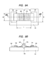
- Figs. 9A and 9B show a construction of the electron-emitting device disclosed in Japanese Patent Application Laid-Open No.2000-231872.
- reference numeral 101 denotes a substrate; 102 and 103 device electrodes; 104 an electroconductive thin film; 105 a carbon film; 106 a groove portion; and 107 an electron-emitting region.
- Fig. 9A is a schematic plan view of such a device.
- Fig. 9B is a schematic cross sectional view taken along the line 9B-9B' in Fig. 9A.
- the device electrodes 102 and 103 are formed on the substrate 101, the continuous electroconductive thin film 104 is formed so as to connect the device electrodes 102 and 103, thereafter, a gap is formed by applying a forming voltage across the device electrodes 102 and 103 (forming step), and the carbon films 105 containing carbon and/or a carbon compound as a main component are further deposited on the electroconductive thin films 104 of the both electrode sides (activating step).
- the groove portion 106 in which a material of the substrate is altered by the heat of the activation is formed.
- Another object of the invention is to provide a manufacturing method of an electron-emitting device which is improved in stability, especially, in high efficiency and a long life, and its manufacturing method.
- an electron-emitting device having a pair of electroconductors arranged on a substrate at an interval, wherein a top of one of the pair of electroconductors is higher than that of the other electroconductor and a groove extending from the interval region toward a position under a region where the one electroconductor is come into contact with the substrate is formed on the substrate along the interval.
- a manufacturing method of an electron-emitting device having a pair of electroconductive members arranged on a substrate at an interval and a film which contains carbon as a main component and covers each of the pair of electroconductive members comprising the step of applying voltage pulses of both polarities across the pair of electroconductive members arranged on the substrate at the interval in an atmosphere containing carbon compound gases, wherein in the voltage pulses of the both polarities, an absolute value of the voltage pulse of the same polarity as that of the voltage pulse applied at the time of driving the electron-emitting device is larger than an absolute value of the voltage pulse of the opposite polarity.
- a manufacturing method of an electron-emitting device having a pair of electroconductive members arranged on a substrate at an interval and a film which contains carbon as a main component and covers each of the pair of electroconductive members comprising the step of applying voltage pulses of both polarities across the pair of electroconductive members arranged on the substrate at the interval in an atmosphere containing carbon compound gases, wherein in the voltage pulses of the both polarities, a quiescent period until the voltage pulse of the same polarity side is applied after applying the voltage pulse of the polarity opposite to that of the voltage pulse applied at the time of driving the electron-emitting device is shorter than a quiescent period until the voltage pulse of the opposite polarity is applied after applying the voltage pulse of the same polarity.
- the first aspect of the invention provides an electron-emitting device having a pair of electroconductors arranged on a substrate at an interval, wherein a top of one of the pair of electroconductors is higher than that of the other electroconductor and a groove extending from the interval region toward a position under a region where the one electroconductor is come into contact with the substrate is formed on the substrate along the interval.
- the second aspect of the invention provides an electron source having a plurality of electron-emitting devices on a substrate, wherein the electron-emitting device is the electron-emitting device according to the first aspect of the invention.
- the third aspect of the invention provides an image display apparatus comprising: an electron source having a plurality of electron-emitting devices on a substrate; and phosphor members which emit light by electrons emitted from the electron-emitting devices, wherein the electron source is the electron source according to the second aspect of the invention.
- the fourth aspect of the invention provides a manufacturing method of an electron-emitting device having a pair of electroconductive members arranged on a substrate at an interval and a film which contains carbon as a main component and covers each of the pair of electroconductive members, comprising the step of applying voltage pulses of both polarities across the pair of electroconductive members arranged on the substrate at the interval in an atmosphere containing carbon compound gases, wherein in the voltage pulses of the both polarities, an absolute value of the voltage pulse of the same polarity as that of the voltage pulse applied at the time of driving the electron-emitting device is larger than an absolute value of the voltage pulse of the opposite polarity.
- the fifth aspect of the invention provides a manufacturing method of an electron-emitting device having a pair of electroconductive members arranged on a substrate at an interval and a film which contains carbon as a main component and covers each of the pair of electroconductive members, comprising the step of applying voltage pulses of both polarities across the pair of electroconductive members arranged on the substrate at the interval in an atmosphere containing carbon compound gases, wherein in the voltage pulses of the both polarities, a quiescent period until the voltage pulse of the same polarity side is applied after applying the voltage pulse of the polarity opposite to that of the voltage pulse applied at the time of driving the electron-emitting device is shorter than a quiescent period until the voltage pulse of the opposite polarity is applied after applying the voltage pulse of the same polarity.
- the sixth aspect of the invention provides a manufacturing method of an electron-emitting device having a pair of electroconductive members arranged on a substrate at an interval and a film which contains carbon as a main component and covers each of the pair of electroconductive members, comprising the step of applying voltage pulses of both polarities across the pair of electroconductive members arranged on the substrate at the interval in an atmosphere containing carbon compound gases, wherein in the voltage pulses of the both polarities, an absolute value of the voltage pulse of the same polarity as that of the voltage pulse applied at the time of driving the electron-emitting device is larger than an absolute value of the voltage pulse of the opposite polarity, and a quiescent period until the voltage pulse of the same polarity side is applied after applying the voltage pulse of the opposite polarity is shorter than a quiescent period until the voltage pulse of the opposite polarity is applied after applying the voltage pulse of the same polarity.
- the seventh aspect of the invention provides a manufacturing method of an electron source having a plurality of electron-emitting devices each comprising a pair of electroconductive members arranged on a substrate at an interval and a film which contains carbon as a main component and covers each of the pair of electroconductive members, wherein the electron-emitting device is manufactured by the manufacturing method of the electron-emitting device according to any one of the fourth to sixth aspects of the invention.
- the eighth aspect of the invention provides a manufacturing method of an image display apparatus comprising: an electron source having a plurality of electron-emitting devices each having a pair of electroconductive members arranged on a substrate at an interval and a film which contains carbon as a main component and covers each of the pair of electroconductive members; and phosphor members which emit light by electrons emitted from the electron-emitting devices, wherein the electron source is manufactured by the manufacturing method of the electron source according to the seventh aspect of the invention.
- the electron-emitting device of the invention has the asymmetrical electron-emitting regions and has a structure in which the deterioration that is caused by the collision of charged particles is suppressed, the electron-emitting characteristics which are more stable than those in the conventional device are obtained. Therefore, the more stable image display apparatus of low electric power consumption and low costs can be obtained by using the electron-emitting device of the invention.
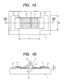
- Figs. 1A and 1B show a construction of an embodiment of the electron-emitting device of the invention.
- reference numeral 1 denotes a substrate; 2 and 3 device electrodes; 4 an electroconductive thin film; 5 a carbon film; 6 a groove portion; and 7 an electron-emitting region.
- Fig. 1A is a schematic plan view of the device.
- Fig. 1B is a schematic cross sectional view taken along the line 1B-1B in Fig. 1A.
- a manufacturing method of the electron-emitting device of the invention will now be described with reference to a manufacturing step of the device shown in Figs. 1A and 1B as an example.
- the device electrodes 2 and 3 are formed on the substrate 1. Quartz glass, glass in which a content of impurities such as Na or the like is reduced, soda lime glass, a substrate obtained by laminating an SiO 2 layer or an SiN layer onto the glass in which the content of impurities such as Na or the like is reduced, ceramics of alumina or the like, an Si substrate, or the like can be used as a substrate 1.
- a metal such as Ni, Cr, Au, Mo, W, Pt, Ti, Al, Cu, Pd, Ru, or the like, an alloy of them, or the like is preferable as a material of the device electrodes 2 and 3, or a print conductor made of a metal oxide and glass or the like or a transparent conductor such as ITO or the like can be used.
- An interval L between the device electrodes 2 and 3, a width W of device electrode, and the like are designed in consideration of a form or the like which is applied.
- the interval L between the device electrodes can be preferably set to a value within a range from hundreds of nm to hundreds of ⁇ m, more preferably, a range from a few ⁇ m to tens of ⁇ m.
- the device electrode width W can be set to a value within a range from a few ⁇ m to hundreds of ⁇ m in consideration of a resistance value of the electrode and the electron-emitting characteristics.
- a film thickness d of each of the device electrodes 2 and 3 can be set to a value within a range from tens of nm to a few ⁇ m.
- the continuous electroconductive thin film 4 connecting the device electrodes 2 and 3 is formed.
- a film thickness of electroconductive thin film 4 is properly selected in consideration of step coverage, processing conditions of a forming step, which will be explained hereinafter, and the like. It is preferably set to a value within a range from 0.1 nm to 100 nm, more preferably, a range from 1 nm to 50 nm.
- a metal such as Pd, Pt, Ru, Ag, Au, Ti, In, Cu, Cr, Fe, Zn, Sn, Ta, W, Pb, or the like; an oxide such as PdO, SnO 2 , In 2 O 3 , PbO, Sb 2 O 3 , RuO 2 , or the like; a boride such as HfB 2 , ZrB 2 , LaB 6 , CeB 6 , YB 4 , GdB 4 , or the like; a carbide such as TiC, ZrC, HfC, TaC, SiC, WC, or the like; a nitride such as TiN, ZrN, HfN, or the like; a semiconductor of Si, Ge, or the like; carbon; or the like.
- a metal such as Pd, Pt, Ru, Ag, Au, Ti, In, Cu, Cr, Fe, Zn, Sn, Ta, W, Pb, or the like
- an oxide such as Pd
- the electroconductive thin film 4 shows a sheet resistance value of 1 ⁇ 10 7 ⁇ / ⁇ or less.
- the sheet resistance value of the electroconductive thin film 4 is limited as a resistance value in which a preferable gap can be formed in the forming step, which will be explained hereinafter.
- the resistance value lies within a range from 1 ⁇ 10 3 to 1 ⁇ 10 7 ⁇ / ⁇ .
- the electron-emitting region 7 After the electron-emitting region 7 is formed, it is preferable that a voltage which is applied through the device electrodes 2 and 3 is sufficiently applied to the electron-emitting region 7. It is more preferable that the resistance value of the electroconductive thin film 4 is smaller.
- the electroconductive thin film 4 is formed as a metal oxide semiconductor thin film having a resistance value in the range from 1 ⁇ 10 3 to 1 ⁇ 10 7 ⁇ / ⁇ , reduced after the forming step, which will be explained hereinafter, and used as a metal thin film having a smaller resistance value.
- a lower limit of the resistance value of the electroconductive thin film 4 in the final state is not particularly limited.
- the resistance value of the electroconductive thin film 4 used here denotes a resistance value which is measured in a region including no gap.
- a forming voltage By applying a forming voltage across the device electrodes 2 and 3, a part of the electroconductive thin film 4 is deformed and altered, thereby forming a gap and forming the electron-emitting region 7. This step is called a forming step.
- a pulse voltage as a voltage which is applied across the device electrodes 2 and 3.
- a pulse peak value is made constant and a case where the voltage is applied while increasing the pulse peak value.
- a method of applying the pulse voltage and a voltage value, a pulse width, and a pulse interval of the pulse voltage which is applied are properly selected in accordance with the material, film thickness, resistance value, and the like of the electroconductive thin film 4. It is also preferable to execute the forming step in the vacuum or in the atmosphere containing a reductive gas such as hydrogen or the like.
- the activating step is executed. Specifically speaking, voltage pulses of both polarities are applied across the device electrodes 2 and 3 in the atmosphere containing carbon compound gases, thereby depositing the carbon film 5 containing carbon as a main component into the gap of the electroconductive thin film 4 and on the electroconductive thin film 4.
- the device electrode 2 and the electroconductive thin film 4 form an electroconductive member
- the device electrode 3 and the electroconductive thin film 4 form an electroconductive member
- the voltage pulses of both polarities are applied across the pair of electroconductive members.
- carbon is, for example, graphite (containing what is called HOPG, PG, and GC:
- HOPG denotes a crystalline structure of almost perfect graphite
- PG denotes a slightly disordered crystalline structure in which a crystal grain is equal to about 20 nm
- GC denotes a further disordered crystalline structure in which a crystal grain is equal to about 2 nm
- amorphous carbon which denotes amorphous carbon and a mixture of amorphous carbon and microcrystal of graphite.
- the invention is characterized in that the pulses of both polarities which are used in the activating step have a predetermined relation with the polarity of the voltage pulse at driving of the electron-emitting device.
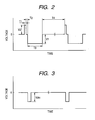
- Fig. 2 shows an example of a waveform of the voltage pulse which is used in the activating step in the invention.
- Fig. 3 shows an example of a waveform of the voltage pulse at driving which is used in combination with Fig. 2.
- the voltage pulses which are used in the activating step in the invention satisfies either the following condition (1) or (2).
- the voltage pulses are set so as to satisfy the relation (T2 ⁇ T4).
- they are set so as to satisfy the relation (
- the pulse waveform is set so as to satisfy both of (1) and (2).
- is set to a value within a range of 20 to 24 V and
- a pulse width T1 is set to a value within a range of 0.01 to 0.2 msec.
- a pulse width T3 is set to a value within a range of 0.1 to 2 msec.
- a pulse interval T2 is set to a value within a range of 0.01 to 0.2 msec.
- a pulse interval T4 is set to a value within a range of 0.01 to 120 msec.
- one period (T1 + T2 + T3 + T4) is set to a value within a range of 2 to 120 msec.
- the carbon films 5 are asymmetrically formed on the electroconductive thin films 4, so that the electron-emitting region 7 is formed.
- an electroconductor comprising the device electrode 2, electroconductive thin film 4, and carbon film 5 and an electroconductor comprising the device electrode 3, electroconductive thin film 4, and carbon film 5 are arranged at an interval and a top (portion which is farthest from the substrate 1) of one electroconductor (on the side of the device electrode 2 in Figs. 1A and 1B) is higher than that of the other electroconductor (on the side of the device electrode 3 in Figs. 1A and 1B).
- the heat upon activation occurs alternately and asymmetrically, alteration of the substrate 1 occurs in a lower portion of the electroconductor (the device electrode 2 + the electroconductive thin film 4). It is, consequently, considered that the groove portion 6 extending from the interval region toward the downward of a region where one electroconductor is come into contact with the substrate is formed along the interval between the electroconductors. As shown in Figs. 1A and 1B, it is desirable that the deepest portion of the groove portion 6 is located under the region where one electroconductor is come into contact with the substrate.
- the electron-emitting device of Figs. 1A and 1B applies the voltage pulse of the same polarity as that upon driving to the device electrode 2 side.
- an aliphatic hydrocarbon class of alkane, alkene, or alkyne, an aromatic hydrocarbon class, an alcohol class, an aldehyde class, a ketone class, an amine class, an organic acid class such as phenol, carvone, or sulfonic acid, or the like can be mentioned.
- saturated hydrocarbon expressed by C n H 2n+2 such as methane, ethane, propane, or the like
- unsaturated hydrocarbon expressed by a composition formula such as C n H 2n of ethylene, propylene, or the like
- benzene; toluene methanol; ethanol; formaldehyde; acetaldehyde; acetone; methylethyl ketone; methylamine; ethylamine; phenol; benzonitrile; trinitrile; formic acid; acetic acid; propionic acid; or the like; or their mixture.
- the electron-emitting device formed as mentioned above has a simple construction and can be easily manufactured, a number of electron-emitting devices can be arranged and formed in a large area. Therefore, by forming a plurality of electron-emitting devices onto the substrate and electrically connecting those electron-emitting devices by wirings, the electron source of the large area can be easily formed.
- FIG. 7 In the electron source in which a plurality of electron-emitting devices are arranged on the substrate, various layouts of the electron-emitting devices can be used.
- an electron source in which electron-emitting devices 74 are arranged in a matrix form as shown in Fig. 7 can be mentioned.
- reference numeral 71 denotes an electron source substrate; 52 row-directional (Y-direction) wirings; 53 column-directional (X-direction) wirings; and 74 the electron-emitting devices.
- One of the electrodes of each of the plurality of electron-emitting devices arranged on the same row is connected to the common row-directional wiring 52.
- the other electrode of each of the plurality of electron-emitting devices arranged on the same column is connected to the common column-directional wiring 53.
- Such a wiring method is called a simple matrix wiring.
- a voltage Vx is applied to the column-directional wiring 53 to which the electron-emitting devices to be driven are connected.
- a voltage -Vy having the polarity opposite to that of the voltage Vx is applied to the row-directional wiring 52 to which the electron-emitting devices to be driven are connected.
- a differential voltage (Vx + Vy) is applied to the electron-emitting devices to be driven.
- the voltage Vx is applied to the electron-emitting devices arranged on the same column as that of the electron-emitting devices to be driven.
- the voltage Vy is applied to the electron-emitting devices arranged on the same row as that of the electron-emitting devices to be driven.
- the image display apparatus can be constructed by combining it with the phosphor members which emit the light by the electrons emitted from the electron-emitting devices.
- Fig. 5 is a schematic plan view of an embodiment of the electron source with the simple matrix construction shown in Fig. 7.
- reference numeral 54 denotes an interlayer insulative layer and the same component elements as those in Figs. 1A, 1B, and 7 are designated by the same reference numerals.
- the carbon film 5 and the groove portion 6 in Figs. 1A and 1B are omitted.
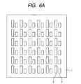
- the substrate 1 is sufficiently cleaned by using a detergent, pure water, organic solvent, and the like and the device electrodes 2 and 3 are formed by using a combination of a vacuum evaporation depositing method, a sputtering method, and a photolithography technique, or a printing method, or the like (Fig. 6A).
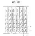
- the column-directional wirings 53 made of an electroconductive material such as a metal or the like are formed on the substrate 1 on which the device electrodes 2 and 3 have been formed by using the combination of the vacuum evaporation depositing method, the sputtering method, and the photolithography technique, or the printing method, or the like (Fig. 6B).
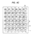
- the interlayer insulative layer 54 made of an insulative material containing silicon oxide, lead oxide, or the like as a main component is formed by using the combination of the vacuum evaporation depositing method, the sputtering method, and the photolithography technique, or the printing method, or the like (Fig. 6C).
- the interlayer insulative layer 54 is formed so as to cover crossing portions of the row-directional wirings 52 and the column-directional wirings 53.
- a material, a film thickness, and a manufacturing method of the interlayer insulative layer 54 are properly set so as to withstand the potential difference between both of those wirings.
- Contact holes 55 to electrically connect the device electrode 2 and the row-directional wirings 52 are formed.
- the row-directional wirings 52 are formed on the interlayer insulative layer 54 in a manner similar to the column-directional wirings 53 (Fig. 6D).
- the row-directional wirings 52 and the column-directional wirings 53 are electrically connected to the pair of device electrodes 2 and 3 of each electron-emitting device.
- the electroconductive thin film 4 is formed between the device electrodes 2 and 3 (Fig. 6E).
- the electroconductive thin film 4 can be formed by: a method whereby the material constructing the electroconductive thin film 4 is formed as a film by the sputtering method, vacuum evaporation depositing method, chemical vapor phase depositing method, or the like; a method whereby the gap between the device electrodes 2 and 3 is coated with a compound solution containing the material constructing the electroconductive thin film 4 by using a dipping method, a spin coating method, an ink-jet coating method, or the like; etc.
- the forming step is executed.
- the forming step can be executed by applying the voltage across the device electrodes 2 and 3 of each electron-emitting device through the row-directional wirings 52 and the column-directional wirings 53.
- the electroconductive thin film 4 of each electron-emitting device is locally destroyed, a gap is caused, and the electron-emitting region 7 is formed (Fig. 5).
- the activating step is executed.
- the activating step is executed by applying the voltage across the device electrodes 2 and 3 of each electron-emitting device through the row-directional wirings 52 and the column-directional wirings 53 in the atmosphere containing the carbon compound.
- carbon and/or carbon compound are/is deposited in the gap formed in the forming step and in the portion around the gap and the carbon film 5 is formed.
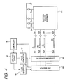
- Fig. 4 is a connection diagram of the voltage applying means and the electron source in the activating step.
- reference numeral 41 denotes an electron source substrate; 42 an activation driver; 43 and 47 pulse generators; 44 a line selector; 45 a current measuring unit; and 46 a controller.
- the pulse generator 43 and the line selector 44 are constructed in such a manner that a pulse oscillating period and a line selection switching period are synchronized by the activation driver 42.
- the pulse voltage generated by the pulse generator 43 is inputted to the line selector 44 and outputted to one of output terminals Sy1 to Sym.
- the output terminals Sy1 to Sym are connected to row-directional wirings Dy1 to Dym of the electron source substrate 41, respectively.
- Column-directional wiring D ⁇ 1 to Dxn are coupled in common and connected to the ground level.
- the output terminals Sy1 to Sym are connected to switches sw1 to swm (not shown), respectively.
- Each switch is connected to either an output portion of the pulse generator 43 or the ground level. The switching operation of each switch is independently controlled by the activation driver 42. Thus, the pulse voltages are sequentially applied to the row-directional wirings of the electron source substrate 41.
- the current measuring unit 45 is a measuring unit of the device current flowing in each of the row-directional wirings Dy1 to Dym. Measurement values of the device currents are read out and inputted to the controller 46.
- the controller 46 controls the operation of the activation driver 42 on the basis of the measurement values. For example, the selection of the row-directional wirings to which the pulse voltages are applied, the waveform of the pulse voltage which is generated from the pulse generator 43, and the like are controlled. For example, the controller 46 controls so that another pulse voltage which is generated from the other pulse generator 47 is applied.
- the activation is performed while sequentially applying the pulse voltages to the row-directional wirings of the electron source substrate 41 as mentioned above.
- the stabilizing step is executed after the activating step.
- This step is a step of exhausting the carbon compound in the vacuum container.
- a vacuum exhauster for exhausting the inside of the vacuum container it is preferable to use an oil-free vacuum exhauster so that an oil which is generated from the exhauster does not exert an influence on characteristics of the device.
- a vacuum exhauster such as absorption pump, ion pump, or the like can be mentioned.
- a partial pressure of the organic component in the vacuum container is a partial pressure at which carbon and carbon compound mentioned above are hardly newly deposited and is preferably set to 1 ⁇ 10 -6 Pa or less, more preferably, 1 ⁇ 10 -8 Pa or less.
- a heating condition at this time is set so that the vacuum container is heated at temperatures of 150 to 350 °C for a processing time as long as possible. It is not, particularly, limited to such a heating condition but a proper heating condition is selected in accordance with various conditions such as size and shape of the vacuum container, construction of the electron-emitting device, and the like.
- the deposition of new carbon or carbon compound can be suppressed and H 2 O, O 2 , and the like adsorbed onto the vacuum container, the substrate, and the like can be also removed, so that a device current If and an emission current Ie become stable.
- reference numeral 81 denotes a rear plate on which the electron source substrate 71 has been fixed; 86 a face plate (phosphor member) on which a phosphor film 84, a metal back 85, and the like have been formed on the inner surface of a glass substrate 83; and 82 a supporting frame.
- the rear plate 81 and the face plate 86 are coupled with the supporting frame 82 by using frit glass or the like of a low melting point.
- Reference numeral 87 denotes a high-voltage terminal and 88 indicates an envelope.
- the envelope 88 is constructed by the face plate 86, supporting frame 82, and rear plate 81 as mentioned above.
- the rear plate 81 is provided mainly to reinforce strength of the electron source substrate 71, if the electron source substrate 71 itself has the sufficient strength, the rear plate 81 which is provided as a separate member can be made unnecessary.
- the envelope 88 having the sufficient strength against the atmospheric pressure can be also constructed.
- the substrate 1 on which a silicon oxide film having a thickness of 500 nm has been formed on soda lime glass by a CVD method is cleaned with a detergent and pure water.
- a lift-off pattern of the device electrodes 2 and 3 is formed by a photoresist (RD-2000N-41 made by Hitachi Chemical Co., Ltd.) and a Ti film having a thickness of 5 nm and a Pt film having a thickness of 100 nm are sequentially deposited by a vacuum evaporation depositing method.
- a pattern of the column-directional wirings 53 is formed and printed by a screen printing method by using a paste material (NP-4028A made by Noritake Co., Ltd.) containing Ag as a metal component. After the printing, the pattern is dried at 110°C for 20 minutes. Subsequently, the paste is baked by a heat treatment apparatus under the conditions of a peak temperature 480°C and a peak holding time of 8 minutes and the column-directional wirings 53 are formed.
- a paste material NP-4028A made by Noritake Co., Ltd.
- a pattern of the interlayer insulative layer 54 is printed by using a paste containing PbO as a main component and the paste is baked under conditions similar to those in step (b), and the interlayer insulative layer 54 is formed.
- the interlayer insulative layer 54 is formed by opening the contact holes 55 to electrically connect the device electrode 2 and the row-directional wirings 52 so as to cover the regions including at least the crossing portions of the row-directional wirings 52 and the column-directional wirings 53.
- a pattern of the row-directional wirings 52 is printed onto the insulative layer 54 by the screen printing method by using a material similar to that of the column-directional wirings 53. After the printing, the pattern is dried at 110°C for 20 minutes. Subsequently, the paste is baked by the heat treatment apparatus under the conditions of the peak temperature 480°C and the peak holding time of 8 minutes and the row-directional wirings 52 are formed.
- a palladium complex solution obtained by dissolving a palladium acetate monoethanol amine complex into a mixture solution of IPA and water
- a heat baking process is executed at 300°C for 15 minutes and the electroconductive thin film 4 made of palladium oxide is formed.
- An average thickness of electroconductive thin film 4 formed in this manner is equal to 8 nm.
- the substrate on which the electron-emitting devices, wirings, and interlayer insulative layers have been formed as mentioned above is put in the vacuum container and the inside of the container is exhausted by a vacuum pump.
- a pressure in the container reaches 2 ⁇ 10 -3 Pa, an exhaust valve is closed.
- 2% H 2 mixture N 2 gases are introduced into the container, a voltage is applied across the row-directional wirings 52 and the column-directional wirings 53 through terminals out of the container and the forming of the electron-emitting devices is executed.
- the forming voltage is set to -14V and has a square wave of a pulse width of 1 msec and a pulse interval of 50 msec.
- the column-directional wirings 53 are connected to the ground level in common and the voltages are applied while the row-directional wirings 52 are sequentially selected.
- a resistance measuring pulse of 1V is inserted between the pulses and a resistance is measured.
- a measured value per device reaches about 1 M ⁇ or more, the supply of the voltage is finished. In this manner, the gap is formed in the electroconductive thin film 4 of each electron-emitting device.
- the 2% H 2 mixture N 2 gases are introduced into the container until the pressure reaches 2 ⁇ 10 -4 Pa. After that, the device is held for 30 minutes and the electroconductive thin film 4 is reduced.
- the inside of the vacuum container is exhausted by the vacuum pump.
- the pressure in the container reaches 2 ⁇ 10 -5 Pa
- trinitrile is introduced into the vacuum container through a slow leakage valve and the pressure of 1.3 ⁇ 10 -4 Pa is maintained.
- the column-directional wirings 53 (Dx1 to Dxn) are connected to the ground level in common through the terminals out of the container, the pulse voltages are sequentially applied to the row-directional wirings 52 (Dy1 to Dym), and the activation operation is executed.
- the pulse voltages in this instance the pulse voltages of the both polarities shown in Fig. 2 are used.
- the foregoing pulses are continuously supplied for 30 minutes. After that, the electron source substrate after the activating step is extracted from the vacuum container and five arbitrary devices are observed with the SEM.
- the structure of an arbitrary electron-emitting region is sliced by using an FIB working technique in order to observe a cross section.
- FIB working technique in order to observe a cross section.
- the electron source substrate after the activating step is put into the vacuum container again. While exhausting the inside of the vacuum container, the electron source substrate is heated at 300°C and the vacuum container is heated at 200°C for 10 hours, and the stabilization operation is executed.
- electron-emitting characteristics are evaluated in this vacuum container.
- the voltage is applied to the electron-emitting device through the terminals out of the container and the device current (If) flowing in the electron-emitting device at this time is measured.
- An anode electrode is attached 2 mm above the electron source substrate and the voltage is applied to the anode electrode.
- the emission current (Ie) emitted from the electron-emitting device is measured.
- the pressure in the vacuum exhauster at the time of measuring the electron-emitting characteristics is equal to 2 ⁇ 10 -8 Pa or less.
- one (D ⁇ 1) of the column-directional wirings 53 is selected and the pulse voltage of +7.5V having a pulse width of 1 msec and a pulse interval of 16.6 msec is applied.
- the pulse voltage of -14V having a pulse width of 1 msec and a pulse interval of 16.6 msec is sequentially applied to the row-directional wirings 52 (Dy1 to Dym) by 10 pulses at a time.
- the pulse voltage of 21.5V is applied to all of the electron-emitting devices by 10 pulses at a time. At this time, unselected wirings are connected to the ground level.
- one (D ⁇ 1) of the column-directional wirings 53 is similarly selected and the pulse voltage of +7.5V having a pulse width of 1 msec and a pulse interval of 16.6 msec is applied.
- the pulse voltage of -10.5V having a pulse width of 1 msec and a pulse interval of 16.6 msec is sequentially applied to the row-directional wirings 52 (Dy1 to Dym) each time for 300 seconds.
- the pulse voltage of 18V is applied to all of the electron-emitting devices, thereby driving the devices.
- the device current (If) flowing in each electron-emitting device at this time is measured, the voltage of 1 kV is applied to the anode electrode, and the emission current (Ie) is measured.
- the column-directional wirings 53 (Dx1 to Dxn) are connected to the ground level in common through the terminals out of the container, the pulse voltages are sequentially applied to the row-directional wirings 52 (Dy1 to Dym), and the activation operation is executed.
- the pulse voltages in this instance the pulse voltages of the both polarities shown in Fig. 2 are used.
- the electron source substrate after the activating step is extracted from the vacuum container and five arbitrary devices are observed with the SEM.
- the structure of an arbitrary electron-emitting region is sliced by using the FIB working technique in order to observe a cross section.
- most of the sliced cross sections have the structure shown in the schematic diagrams of Figs. 1A and 1B, the groove portion 6 exists obliquely, and the deepest portion of the groove portion 6 is located under the Pd thin film.
- the electron source substrate is put into the vacuum container again. While exhausting the inside of the vacuum container, the electron source substrate is heated at 300°C and the vacuum container is heated at 200°C for 10 hours, and the stabilization operation is executed.
- electron-emitting characteristics are evaluated in this vacuum container.
- the voltage is applied to the electron-emitting device through the terminals out of the container and the device current (If) flowing in the electron-emitting device at this time is measured.
- the anode electrode is attached 2 mm above the electron source substrate and the voltage is applied to the anode electrode.
- the emission current (Ie) emitted from the electron-emitting device is measured.
- the pressure in the vacuum exhauster at the time of measuring the electron-emitting characteristics is equal to 2 ⁇ 10 -8 Pa or less.
- one (Dx1) of the column-directional wirings 53 is selected and the pulse voltage of +7.5V having a pulse width of 1 msec and a pulse interval of 16.6 msec is applied.
- the pulse voltage of -15V having a pulse width of 1 msec and a pulse interval of 16.6 msec is sequentially applied to the row-directional wirings 52 (Dy1 to Dym) by 10 pulses at a time.
- the pulse voltage of 22.5V is applied to all of the electron-emitting devices by 10 pulses at a time. At this time, unselected wirings are connected to the ground level.
- one (Dx1) of the column-directional wirings 53 is similarly selected and the pulse voltage of +7.5V having a pulse width of 1 msec and a pulse interval of 16.6 msec is applied.
- the pulse voltage of -11.5V having a pulse width of 1 msec and a pulse interval of 16.6 msec is sequentially applied to the row-directional wirings 52 (Dy1 to Dym) each time for 60 seconds.
- the pulse voltage of 19V is applied to all of the electron-emitting devices, thereby driving the devices.
- the device current (If) flowing in each electron-emitting device at this time is measured, the voltage of 1 kV is applied to the anode electrode, and the emission current (Ie) is measured.
- An average value of electron-emitting efficiency (Ie/If) obtained from the measured device currents (If) and emission currents (Ie) is equal to 0.5% and it shows that excellent electron-emitting characteristics are obtained.
- the electron source substrate 71 obtained by executing the processes up to the activating step is formed.
- the face plate 86 is fixed 2 mm above the electron source substrate 71 through the supporting frame 82 and an exhaust pipe (not shown) and the envelope 88 is formed.
- a spacer (not shown) is arranged between the rear plate 81 and the face plate 86, thereby forming a structure which can withstand the atmospheric pressure.
- a getter (not shown) to keep the inside of the container in a high vacuum state is arranged in the envelope 88. Frit glass is used to joint the rear plate 81, the supporting frame 82, and the face plate 86 and they are seal-bonded by heating to 420°C in an argon atmosphere.
- the temperature is dropped to the room temperature and the inside is set to a pressure of about 10 -7 Pa.
- the exhaust pipe is heated by a gas burner, thereby melt-bonding it and sealing the envelope 88.
- the getter is highfrequency-heated and a getter process is executed.
- the image display apparatus as shown in Fig. 8 is manufactured in this manner.
- the preliminary driving is executed in a manner similar to the embodiment 2 and the device current, the emission current, and a non-selection current are measured in a manner similar to the embodiment 2, so that characteristics similar to those in the embodiment 2 are obtained.
- the electron-emitting devices are sequentially driven.
- a pulse voltage of +7.5V is used for the information signal and a pulse voltage of -11.5V is used for the scanning signal.
- the emission electron is made to collide with the phosphor film 84 so as to be excited and emit the light, thereby displaying an image.
- the electron-emitting efficiency at an anode voltage of 10 kV is equal to a high value of 5% and the bright image can be displayed.
- a luminance deterioration is measured after driving the panel for 1000 hours, so that it has been found that a change ratio is equal to 5% or less.
- the inside of the vacuum container is exhausted by the vacuum pump.
- the pressure in the container reaches 2 ⁇ 10 -5 Pa, trinitrile is introduced into the vacuum container through the slow leakage valve and the pressure of 6 ⁇ 10 -4 Pa is maintained.
- the column-directional wirings 53 (Dx1 to Dxn) are connected to the ground level in common through the terminals out of the container, the pulse voltages are sequentially applied to the row-directional wirings 52 (Dy1 to Dym), and the activation operation is executed.
- the pulse voltages in this instance the pulse voltages of the both polarities shown in Fig. 2 are used.
- the electron source substrate after the activating step is extracted from the vacuum container and five arbitrary devices are observed with the SEM.
- the structure of an arbitrary electron-emitting region is sliced by using the FIB working technique in order to observe a cross section.
- most of the sliced cross sections have the structure shown in the schematic diagrams of Figs. 1A and 1B, the groove portion 6 exists obliquely, and the deepest portion of the groove portion 6 is located under the Pd thin film.
- the electron source substrate is put into the vacuum container again. While exhausting the inside of the vacuum container, the electron source substrate is heated at 300°C and the vacuum container is heated at 200°C for 10 hours, and the stabilization operation is executed.
- electron-emitting characteristics are evaluated in this vacuum container.
- the voltage is applied to the electron-emitting device through the terminals out of the container and the device current (If) flowing in the electron-emitting device at this time is measured.
- the anode electrode is attached 2 mm above the electron source substrate and the voltage is applied to the anode electrode.
- the emission current (Ie) emitted from the electron-emitting device is measured.
- the pressure in the vacuum exhauster at the time of measuring the electron-emitting characteristics is equal to 2 ⁇ 10 -8 Pa or less.
- one (Dx1) of the column-directional wirings 53 is selected and the pulse voltage of +7.5V having a pulse width of 0.01 msec and a pulse interval of 16.6 msec is applied.
- the pulse voltage of -15V having a pulse width of 1 msec and a pulse interval of 16.6 msec is sequentially applied to the row-directional wirings 52 (Dy1 to Dym) by 10 pulses at a time.
- the pulse voltage of 22.5V is applied to all of the electron-emitting devices by 1000 pulses at a time. At this time, unselected wirings are connected to the ground level.
- one (Dx1) of the column-directional wirings 53 is similarly selected and the pulse voltage of +7.5V having a pulse width of 1 msec and a pulse interval of 16.6 msec is applied.
- the pulse voltage of -11.5V having a pulse width of 0.1 msec and a pulse interval of 16.6 msec is sequentially applied to the row-directional wirings 52 (Dy1 to Dym) each time for 60 seconds.
- the pulse voltage of 19V is applied to all of the electron-emitting devices, thereby driving the devices.
- the device current (If) flowing in each electron-emitting device at this time is measured, the voltage of 1 kV is applied to the anode electrode, and the emission current (Ie) is measured.
- An average value of electron-emitting efficiency (Ie/If) obtained from the measured device currents (If) and emission currents (Ie) is equal to 0.6% and it shows that excellent electron-emitting characteristics are obtained.
- the electron source substrate 71 obtained by executing the processes up to the activating step is formed.
- the face plate 86 is fixed 2 mm above the electron source substrate 71 through the supporting frame 82 and the exhaust pipe (not shown) and the envelope 88 is formed.
- the spacer (not shown) is arranged between the rear plate 81 and the face plate 86, thereby forming the structure which can withstand the atmospheric pressure.
- the getter (not shown) to keep the inside of the container in a high vacuum state is arranged in the envelope 88.
- the frit glass is used to joint the rear plate 81, the supporting frame 82, and the face plate 86 and they are seal-bonded by heating to 420°C in the vacuum atmosphere.
- the temperature is dropped to the room temperature and the inside is set to a pressure of about 10 -7 Pa.
- the exhaust pipe is heated by the gas burner, thereby melt-bonding it and sealing the envelope 88.
- the getter is highfrequency heated and the getter process is executed.
- the image display apparatus as shown in Fig. 8 is manufactured in this manner.
- the preliminary driving is executed in a manner similar to the embodiment 2 and the device current, the emission current, and a non-selection current are measured in a manner similar to the embodiment 2, so that characteristics similar to those in the embodiment 2 are obtained.
- the electron-emitting devices are sequentially driven.
- the pulse voltage of +7.5V is used for the information signal and the pulse voltage of - 11.5V is used for the scanning signal.
- the emission electron is made to collide with the phosphor film 84 so as to be excited and emit the light, thereby displaying an image.
- the electron-emitting efficiency at the anode voltage of 10 kV is equal to a high value of 4% and the bright image can be displayed.
- a luminance deterioration is measured after driving the panel for 800 hours, so that it has been found that a change ratio is equal to 5% or less.
- the inside of the vacuum container is exhausted by the vacuum pump.
- the pressure in the container reaches 2 ⁇ 10 -5 Pa, trinitrile is introduced into the vacuum container through the slow leakage valve and the pressure of 6 ⁇ 10 -4 Pa is maintained.
- the column-directional wirings 53 (Dx1 to Dxn) are connected to the ground level in common through the terminals out of the container, the pulse voltages are sequentially applied to the row-directional wirings 52 (Dy1 to Dym), and the activation operation is executed.
- the pulse voltages in this instance the pulse voltages of the both polarities shown in Fig. 2 are used.
- the electron source substrate after the activating step is extracted from the vacuum container and five arbitrary devices are observed with the SEM.
- the structure of an arbitrary electron-emitting region is sliced by using the FIB working technique in order to observe a cross section.
- the FIB working technique in order to observe a cross section.
- the electron source substrate is put into the vacuum container again. While exhausting the inside of the vacuum container, the electron source substrate is heated at 300°C and the vacuum container is heated at 200°C for 10 hours, and the stabilization operation is executed.
- electron-emitting characteristics are evaluated in this vacuum container.
- the voltage is applied to the electron-emitting device through the terminals out of the container and the device current (If) flowing in the electron-emitting device at this time is measured.
- the anode electrode is attached 2 mm above the electron source substrate and the voltage is applied to the anode electrode.
- the emission current (Ie) emitted from the electron-emitting device is measured.
- the pressure in the vacuum exhauster at the time of measuring the electron-emitting characteristics is equal to 2 ⁇ 10 -8 Pa or less.
- one (Dx1) of the column-directional wirings 53 is selected and the pulse voltage of +7.5V having a pulse width of 0.01 msec and a pulse interval of 16.6 msec is applied.
- the pulse voltage of -15V having a pulse width of 1 msec and a pulse interval of 16.6 msec is sequentially applied to the row-directional wirings 52 (Dy1 to Dym) by 10 pulses at a time.
- the pulse voltage of 22.5V is applied to all of the electron-emitting devices by 100 pulses at a time. At this time, unselected wirings are connected to the ground level.
- one (Dx1) of the column-directional wirings 53 is similarly selected and the pulse voltage of +7.5V having a pulse width of 1 msec and a pulse interval of 16.6 msec is applied.
- the pulse voltage of -11.5V having a pulse width of 0.1 msec and a pulse interval of 16.6 msec is sequentially applied to the row-directional wirings 52 (Dy1 to Dym) each time for 60 seconds.
- the pulse voltage of 19V is applied to all of the electron-emitting devices, thereby driving the devices.
- the device current (If) flowing in each electron-emitting device is measured, the voltage of 1 kV is applied to the anode electrode, and the emission current (Ie) is measured.
- An average value of electron-emitting efficiency (Ie/If) obtained from the measured device currents (If) and emission currents (Ie) is equal to 0.5% and it shows that excellent electron-emitting characteristics are obtained.
- the electron source substrate 71 obtained by executing the processes up to the activating step is formed.
- the face plate 86 is fixed 2 mm above the electron source substrate 71 through the supporting frame 82 and the exhaust pipe (not shown) and the envelope 88 is formed.
- the spacer (not shown) is arranged between the rear plate 81 and the face plate 86, thereby forming the structure which can withstand the atmospheric pressure.
- the getter (not shown) to keep the inside of the container in a high vacuum state is arranged in the envelope 88.
- the frit glass is used to joint the rear plate 81, the supporting frame 82, and the face plate 86 and they are seal-bonded by heating to 420°C in the vacuum atmosphere.
- the temperature is dropped to the room temperature and the inside is set to a pressure of about 10 -7 Pa.
- the exhaust pipe is heated by the gas burner, thereby melt-bonding it and sealing the envelope 88.
- the getter is highfrequency heated and the getter process is executed.
- the image display apparatus as shown in Fig. 8 is manufactured in this manner.
- the preliminary driving is executed in a manner similar to the embodiment 2 and the device current, the emission current, and a non-selection current are measured in a manner similar to the embodiment 2, so that characteristics similar to those in the embodiment 2 are obtained.
- the electron-emitting devices are sequentially driven.
- the pulse voltage of +7.5V is used for the information signal and the pulse voltage of - 11.5V is used for the scanning signal.
- the emission electron is made to collide with the phosphor film 84 so as to be excited and emit the light, thereby displaying an image.
- the electron-emitting efficiency at the anode voltage of 10 kV is equal to a high value of 4% and the bright image can be displayed.
- a luminance deterioration is measured after driving the panel for 1000 hours, so that it has been found that a change ratio is equal to 5% or less.
- an electron-emitting device having a pair of electroconductors arranged on a substrate at an interval, a top of one electroconductor is higher than that of the other electroconductor and a groove extending from the interval region toward a position under a region where the one electroconductor is come into contact with the substrate is formed on the substrate. Deterioration of the electron-emitting device due to collision of charged particles is suppressed by the asymmetrical electron-emitting region, electron-emitting efficiency is improved, and a long life is realized.
Landscapes
- Engineering & Computer Science (AREA)
- General Engineering & Computer Science (AREA)
- Life Sciences & Earth Sciences (AREA)
- Environmental Sciences (AREA)
- Manufacturing & Machinery (AREA)
- Environmental & Geological Engineering (AREA)
- Biodiversity & Conservation Biology (AREA)
- Animal Husbandry (AREA)
- Zoology (AREA)
- Marine Sciences & Fisheries (AREA)
- Ocean & Marine Engineering (AREA)
- Mechanical Engineering (AREA)
- Civil Engineering (AREA)
- Structural Engineering (AREA)
- Cold Cathode And The Manufacture (AREA)
- Cathode-Ray Tubes And Fluorescent Screens For Display (AREA)
Applications Claiming Priority (2)
| Application Number | Priority Date | Filing Date | Title |
|---|---|---|---|
| JP2004127646 | 2004-04-23 | ||
| JP2004127646 | 2004-04-23 |
Publications (2)
| Publication Number | Publication Date |
|---|---|
| EP1596409A1 true EP1596409A1 (de) | 2005-11-16 |
| EP1596409B1 EP1596409B1 (de) | 2010-05-26 |
Family
ID=34935544
Family Applications (1)
| Application Number | Title | Priority Date | Filing Date |
|---|---|---|---|
| EP05008780A Expired - Lifetime EP1596409B1 (de) | 2004-04-23 | 2005-04-21 | Elektronen-emittierende Vorrichtung, Elektronenquelle, Bildanzeigegerät und Verfahren zur deren Herstellung |
Country Status (5)
| Country | Link |
|---|---|
| US (2) | US7230372B2 (de) |
| EP (1) | EP1596409B1 (de) |
| KR (1) | KR100721872B1 (de) |
| CN (1) | CN100461326C (de) |
| DE (1) | DE602005021429D1 (de) |
Families Citing this family (16)
| Publication number | Priority date | Publication date | Assignee | Title |
|---|---|---|---|---|
| JP3740485B2 (ja) * | 2004-02-24 | 2006-02-01 | キヤノン株式会社 | 電子放出素子、電子源、画像表示装置の製造方法及び駆動方法 |
| US7271529B2 (en) * | 2004-04-13 | 2007-09-18 | Canon Kabushiki Kaisha | Electron emitting devices having metal-based film formed over an electro-conductive film element |
| JP4366235B2 (ja) | 2004-04-21 | 2009-11-18 | キヤノン株式会社 | 電子放出素子、電子源及び画像表示装置の製造方法 |
| JP3907667B2 (ja) * | 2004-05-18 | 2007-04-18 | キヤノン株式会社 | 電子放出素子、電子放出装置およびそれを用いた電子源並びに画像表示装置および情報表示再生装置 |
| JP3774723B2 (ja) | 2004-07-01 | 2006-05-17 | キヤノン株式会社 | 電子放出素子の製造方法およびそれを用いた電子源並びに画像表示装置の製造方法、該製造方法によって製造された画像表示装置を用いた情報表示再生装置 |
| JP4594077B2 (ja) * | 2004-12-28 | 2010-12-08 | キヤノン株式会社 | 電子放出素子及びそれを用いた電子源並びに画像表示装置および情報表示再生装置 |
| KR101107134B1 (ko) * | 2005-08-26 | 2012-01-31 | 삼성에스디아이 주식회사 | 전자 방출 소자, 전자 방출 디바이스 및 그 제조 방법 |
| JP2008258108A (ja) * | 2007-04-09 | 2008-10-23 | Hitachi Ltd | 画像表示装置およびその製造方法 |
| JP2009277459A (ja) * | 2008-05-14 | 2009-11-26 | Canon Inc | 電子放出素子及び画像表示装置 |
| JP4458380B2 (ja) * | 2008-09-03 | 2010-04-28 | キヤノン株式会社 | 電子放出素子およびそれを用いた画像表示パネル、画像表示装置並びに情報表示装置 |
| JP2010092843A (ja) * | 2008-09-09 | 2010-04-22 | Canon Inc | 電子線装置およびそれを用いた画像表示装置 |
| JP2010146914A (ja) * | 2008-12-19 | 2010-07-01 | Canon Inc | 電子放出素子の製造方法および画像表示装置の製造方法 |
| JP4637233B2 (ja) * | 2008-12-19 | 2011-02-23 | キヤノン株式会社 | 電子放出素子の製造方法及びこれを用いた画像表示装置の製造方法 |
| JP2010182585A (ja) * | 2009-02-06 | 2010-08-19 | Canon Inc | 電子放出素子及びこれを用いた画像表示装置 |
| US8284012B2 (en) * | 2009-06-04 | 2012-10-09 | The Aerospace Corporation | Ultra-stable refractory high-power thin film resistors for space applications |
| CN104638522B (zh) * | 2015-01-30 | 2017-01-25 | 王东 | 负离子激活器 |
Citations (4)
| Publication number | Priority date | Publication date | Assignee | Title |
|---|---|---|---|---|
| US6409563B1 (en) * | 1999-02-23 | 2002-06-25 | Canon Kabushiki Kaisha | Electron-emitting device manufacturing method and apparatus, driving method, and adjusting method |
| US20020117670A1 (en) * | 2001-02-27 | 2002-08-29 | Takahiro Horiguchi | Method of manufacturing image-forming apparatus |
| EP1324366A2 (de) * | 2001-12-25 | 2003-07-02 | Canon Kabushiki Kaisha | Elektronenemittierende Vorrichtung, Elektronenquelle und Bildanzeigevorrichtung und Verfahren zur Herstellung |
| EP1347487A2 (de) * | 1998-12-08 | 2003-09-24 | Canon Kabushiki Kaisha | Elektronenemittierende Vorrichtung, Elektronenquelle die diese elektronenemittierenden Vorrichtungen verwendet, und Bilderzeugungsgerät mit dieser Elektronenquelle |
Family Cites Families (31)
| Publication number | Priority date | Publication date | Assignee | Title |
|---|---|---|---|---|
| JP3147267B2 (ja) * | 1993-08-30 | 2001-03-19 | キヤノン株式会社 | 電子放出素子およびその製造方法 |
| JP3072825B2 (ja) * | 1994-07-20 | 2000-08-07 | キヤノン株式会社 | 電子放出素子、電子源、及び、画像形成装置の製造方法 |
| JP3332676B2 (ja) * | 1994-08-02 | 2002-10-07 | キヤノン株式会社 | 電子放出素子、電子源及び画像形成装置と、それらの製造方法 |
| JP2903295B2 (ja) * | 1994-08-29 | 1999-06-07 | キヤノン株式会社 | 電子放出素子、それを用いた電子源並びに画像形成装置と、それらの製造方法 |
| US6246168B1 (en) * | 1994-08-29 | 2001-06-12 | Canon Kabushiki Kaisha | Electron-emitting device, electron source and image-forming apparatus as well as method of manufacturing the same |
| AU712966B2 (en) * | 1994-09-22 | 1999-11-18 | Canon Kabushiki Kaisha | Electron-emitting device and method of manufacturing the same as well as electron source and image forming apparatus comprising such electron-emitting device |
| EP0955663B1 (de) * | 1995-03-13 | 2005-09-21 | Canon Kabushiki Kaisha | Herstellungsverfahren einer Elektronenemittierenden Vorrichtung, einer Elektronenquelle und eines Bilderzeugungsgeräts |
| JP3174999B2 (ja) * | 1995-08-03 | 2001-06-11 | キヤノン株式会社 | 電子放出素子、電子源、それを用いた画像形成装置、及びそれらの製造方法 |
| JP3376220B2 (ja) * | 1995-10-03 | 2003-02-10 | キヤノン株式会社 | 画像形成装置とその製造方法 |
| US6220912B1 (en) * | 1997-05-09 | 2001-04-24 | Canon Kabushiki Kaisha | Method and apparatus for producing electron source using dispenser to produce electron emitting portions |
| DE69919242T2 (de) * | 1998-02-12 | 2005-08-11 | Canon K.K. | Verfahren zur Herstellung eines elektronenemittierenden Elementes, Elektronenquelle und Bilderzeugungsgerätes |
| JPH11283493A (ja) | 1998-03-30 | 1999-10-15 | Canon Inc | 電子放出素子、電子源、画像形成装置及びそれらの製造方法 |
| JP3320387B2 (ja) * | 1998-09-07 | 2002-09-03 | キヤノン株式会社 | 電子源の製造装置及び製造方法 |
| JP2000155555A (ja) * | 1998-09-16 | 2000-06-06 | Canon Inc | 電子放出素子の駆動方法及び、該電子放出素子を用いた電子源の駆動方法、並びに該電子源を用いた画像形成装置の駆動方法 |
| JP3135118B2 (ja) * | 1998-11-18 | 2001-02-13 | キヤノン株式会社 | 電子源形成用基板、電子源及び画像形成装置並びにそれらの製造方法 |
| JP3131782B2 (ja) * | 1998-12-08 | 2001-02-05 | キヤノン株式会社 | 電子放出素子、電子源並びに画像形成装置 |
| WO2000044022A1 (fr) * | 1999-01-19 | 2000-07-27 | Canon Kabushiki Kaisha | Canon d'électrons et imageur et procédé de fabrication, procédé et dispositif de fabrication de source d'électrons, et appareil de fabrication d'imageur |
| JP2000251624A (ja) * | 1999-02-25 | 2000-09-14 | Canon Inc | 電子放出素子及びその製造方法、並びに該電子放出素子を用いた電子源、画像形成装置 |
| JP3652160B2 (ja) * | 1999-02-25 | 2005-05-25 | キヤノン株式会社 | 電子放出素子及び電子源及び画像形成装置及び電子放出素子の製造方法 |
| JP3423661B2 (ja) * | 1999-02-25 | 2003-07-07 | キヤノン株式会社 | 電子放出素子、電子源および画像形成装置の製造方法 |
| JP3323850B2 (ja) * | 1999-02-26 | 2002-09-09 | キヤノン株式会社 | 電子放出素子およびこれを用いた電子源およびこれを用いた画像形成装置 |
| JP3323851B2 (ja) * | 1999-02-26 | 2002-09-09 | キヤノン株式会社 | 電子放出素子およびこれを用いた電子源およびこれを用いた画像形成装置 |
| JP3323849B2 (ja) * | 1999-02-26 | 2002-09-09 | キヤノン株式会社 | 電子放出素子およびこれを用いた電子源およびこれを用いた画像形成装置 |
| JP3323848B2 (ja) * | 1999-02-26 | 2002-09-09 | キヤノン株式会社 | 電子放出素子およびこれを用いた電子源およびこれを用いた画像形成装置 |
| JP3323852B2 (ja) * | 1999-02-26 | 2002-09-09 | キヤノン株式会社 | 電子放出素子およびこれを用いた電子源およびこれを用いた画像形成装置 |
| JP3696083B2 (ja) * | 2000-12-25 | 2005-09-14 | 株式会社東芝 | 平面型電子放出素子 |
| JP3740485B2 (ja) * | 2004-02-24 | 2006-02-01 | キヤノン株式会社 | 電子放出素子、電子源、画像表示装置の製造方法及び駆動方法 |
| US7271529B2 (en) * | 2004-04-13 | 2007-09-18 | Canon Kabushiki Kaisha | Electron emitting devices having metal-based film formed over an electro-conductive film element |
| JP4366235B2 (ja) * | 2004-04-21 | 2009-11-18 | キヤノン株式会社 | 電子放出素子、電子源及び画像表示装置の製造方法 |
| JP3907667B2 (ja) * | 2004-05-18 | 2007-04-18 | キヤノン株式会社 | 電子放出素子、電子放出装置およびそれを用いた電子源並びに画像表示装置および情報表示再生装置 |
| JP3774723B2 (ja) * | 2004-07-01 | 2006-05-17 | キヤノン株式会社 | 電子放出素子の製造方法およびそれを用いた電子源並びに画像表示装置の製造方法、該製造方法によって製造された画像表示装置を用いた情報表示再生装置 |
-
2005
- 2005-04-15 US US11/106,636 patent/US7230372B2/en not_active Expired - Fee Related
- 2005-04-21 DE DE602005021429T patent/DE602005021429D1/de not_active Expired - Lifetime
- 2005-04-21 KR KR1020050032938A patent/KR100721872B1/ko not_active Expired - Fee Related
- 2005-04-21 EP EP05008780A patent/EP1596409B1/de not_active Expired - Lifetime
- 2005-04-22 CN CNB2005100676918A patent/CN100461326C/zh not_active Expired - Fee Related
-
2007
- 2007-01-10 US US11/621,658 patent/US7582002B2/en not_active Expired - Fee Related
Patent Citations (4)
| Publication number | Priority date | Publication date | Assignee | Title |
|---|---|---|---|---|
| EP1347487A2 (de) * | 1998-12-08 | 2003-09-24 | Canon Kabushiki Kaisha | Elektronenemittierende Vorrichtung, Elektronenquelle die diese elektronenemittierenden Vorrichtungen verwendet, und Bilderzeugungsgerät mit dieser Elektronenquelle |
| US6409563B1 (en) * | 1999-02-23 | 2002-06-25 | Canon Kabushiki Kaisha | Electron-emitting device manufacturing method and apparatus, driving method, and adjusting method |
| US20020117670A1 (en) * | 2001-02-27 | 2002-08-29 | Takahiro Horiguchi | Method of manufacturing image-forming apparatus |
| EP1324366A2 (de) * | 2001-12-25 | 2003-07-02 | Canon Kabushiki Kaisha | Elektronenemittierende Vorrichtung, Elektronenquelle und Bildanzeigevorrichtung und Verfahren zur Herstellung |
Also Published As
| Publication number | Publication date |
|---|---|
| US20050236965A1 (en) | 2005-10-27 |
| KR20060047297A (ko) | 2006-05-18 |
| DE602005021429D1 (de) | 2010-07-08 |
| KR100721872B1 (ko) | 2007-05-25 |
| US20070176532A1 (en) | 2007-08-02 |
| US7230372B2 (en) | 2007-06-12 |
| US7582002B2 (en) | 2009-09-01 |
| CN100461326C (zh) | 2009-02-11 |
| EP1596409B1 (de) | 2010-05-26 |
| CN1691244A (zh) | 2005-11-02 |
Similar Documents
| Publication | Publication Date | Title |
|---|---|---|
| US7582002B2 (en) | Manufacturing method of electron emitting device, electron source and image display apparatus | |
| JP3241613B2 (ja) | 電子放出素子、電子源および画像形成装置の製造方法 | |
| KR20010089266A (ko) | 전자선 장치의 제조방법, 화상 형성장치의 제조방법, 이들제조방법에 의해 제조된 전자선 장치 및 화상 형성장치,전자원의 제조방법, 전자원의 제조장치 및 화상형성장치의 제조장치 | |
| JP4366235B2 (ja) | 電子放出素子、電子源及び画像表示装置の製造方法 | |
| EP2120246A2 (de) | Elektronenemittierende Vorrichtung und Bildanzeigevorrichtung | |
| US8013511B2 (en) | Highly-efficient electron-emitting device and image display apparatus having a substrate with a distribution of nitrogen containing ratio | |
| KR100371064B1 (ko) | 전자 방출 소자의 제조 장치 | |
| JP3740485B2 (ja) | 電子放出素子、電子源、画像表示装置の製造方法及び駆動方法 | |
| JP3919792B2 (ja) | 電子放出素子、電子源、画像表示装置、及び、それらの製造方法 | |
| JP3559689B2 (ja) | 電子放出素子、電子源、画像形成装置及びそれらの製造方法 | |
| JP2000195415A (ja) | 電子放出素子、電子源、画像形成装置及びそれらの製造方法 | |
| JP3689683B2 (ja) | 電子放出素子、電子源および画像形成装置の製造方法 | |
| JP2000200544A (ja) | 電子放出素子の製造方法、および電子源と画像形成装置の製造方法 | |
| JP2009043568A (ja) | 電子放出素子及び画像表示装置 | |
| JP3673668B2 (ja) | 電子源の製造方法及び電子源の製造装置 | |
| JP3592032B2 (ja) | 電子放出素子、電子源および画像形成装置の製造方法 | |
| JP2000231876A (ja) | 電子放出素子、電子源、画像形成装置及びそれらの製造方法 | |
| JP2006134592A (ja) | 電子放出素子、電子源、及び、画像形成装置の製造方法 | |
| JP2000243241A (ja) | 電子放出素子の製造方法及び画像形成装置の製造方法 | |
| JP2000164118A (ja) | 表面伝導型電子放出素子、電子源、画像形成装置の製造方法及びその製造に用いる液滴付与装置 | |
| JP2003086083A (ja) | 電子放出素子、電子源基板、画像形成装置、及びそれらの製造方法 | |
| JP2004207124A (ja) | 電子放出素子の製造方法 | |
| JP2000149770A (ja) | 表面伝導型電子放出素子、電子源、画像形成装置の製造方法 | |
| JP2002075169A (ja) | 電子放出素子、電子源、および画像形成装置、並びにそれらの製造方法 | |
| JP2000021290A (ja) | 電子放出素子、電子源、画像形成装置及びそれらの製造方法 |
Legal Events
| Date | Code | Title | Description |
|---|---|---|---|
| PUAI | Public reference made under article 153(3) epc to a published international application that has entered the european phase |
Free format text: ORIGINAL CODE: 0009012 |
|
| AK | Designated contracting states |
Kind code of ref document: A1 Designated state(s): AT BE BG CH CY CZ DE DK EE ES FI FR GB GR HU IE IS IT LI LT LU MC NL PL PT RO SE SI SK TR |
|
| AX | Request for extension of the european patent |
Extension state: AL BA HR LV MK YU |
|
| 17P | Request for examination filed |
Effective date: 20060516 |
|
| AKX | Designation fees paid |
Designated state(s): DE FR GB IT NL |
|
| 17Q | First examination report despatched |
Effective date: 20061214 |
|
| GRAP | Despatch of communication of intention to grant a patent |
Free format text: ORIGINAL CODE: EPIDOSNIGR1 |
|
| GRAS | Grant fee paid |
Free format text: ORIGINAL CODE: EPIDOSNIGR3 |
|
| GRAA | (expected) grant |
Free format text: ORIGINAL CODE: 0009210 |
|
| AK | Designated contracting states |
Kind code of ref document: B1 Designated state(s): DE FR GB IT NL |
|
| REG | Reference to a national code |
Ref country code: GB Ref legal event code: FG4D |
|
| REF | Corresponds to: |
Ref document number: 602005021429 Country of ref document: DE Date of ref document: 20100708 Kind code of ref document: P |
|
| REG | Reference to a national code |
Ref country code: NL Ref legal event code: VDEP Effective date: 20100526 |
|
| PG25 | Lapsed in a contracting state [announced via postgrant information from national office to epo] |
Ref country code: NL Free format text: LAPSE BECAUSE OF FAILURE TO SUBMIT A TRANSLATION OF THE DESCRIPTION OR TO PAY THE FEE WITHIN THE PRESCRIBED TIME-LIMIT Effective date: 20100526 |
|
| PG25 | Lapsed in a contracting state [announced via postgrant information from national office to epo] |
Ref country code: IT Free format text: LAPSE BECAUSE OF FAILURE TO SUBMIT A TRANSLATION OF THE DESCRIPTION OR TO PAY THE FEE WITHIN THE PRESCRIBED TIME-LIMIT Effective date: 20100526 |
|
| PLBE | No opposition filed within time limit |
Free format text: ORIGINAL CODE: 0009261 |
|
| STAA | Information on the status of an ep patent application or granted ep patent |
Free format text: STATUS: NO OPPOSITION FILED WITHIN TIME LIMIT |
|
| 26N | No opposition filed |
Effective date: 20110301 |
|
| REG | Reference to a national code |
Ref country code: DE Ref legal event code: R097 Ref document number: 602005021429 Country of ref document: DE Effective date: 20110228 |
|
| PGFP | Annual fee paid to national office [announced via postgrant information from national office to epo] |
Ref country code: GB Payment date: 20130418 Year of fee payment: 9 Ref country code: DE Payment date: 20130430 Year of fee payment: 9 |
|
| PGFP | Annual fee paid to national office [announced via postgrant information from national office to epo] |
Ref country code: FR Payment date: 20130517 Year of fee payment: 9 |
|
| REG | Reference to a national code |
Ref country code: DE Ref legal event code: R119 Ref document number: 602005021429 Country of ref document: DE |
|
| GBPC | Gb: european patent ceased through non-payment of renewal fee |
Effective date: 20140421 |
|
| REG | Reference to a national code |
Ref country code: FR Ref legal event code: ST Effective date: 20141231 |
|
| REG | Reference to a national code |
Ref country code: DE Ref legal event code: R119 Ref document number: 602005021429 Country of ref document: DE Effective date: 20141101 |
|
| PG25 | Lapsed in a contracting state [announced via postgrant information from national office to epo] |
Ref country code: GB Free format text: LAPSE BECAUSE OF NON-PAYMENT OF DUE FEES Effective date: 20140421 Ref country code: DE Free format text: LAPSE BECAUSE OF NON-PAYMENT OF DUE FEES Effective date: 20141101 |
|
| PG25 | Lapsed in a contracting state [announced via postgrant information from national office to epo] |
Ref country code: FR Free format text: LAPSE BECAUSE OF NON-PAYMENT OF DUE FEES Effective date: 20140430 |