EP1580723A2 - Elektrooptische Anzeigevorrichtung und elektronisches Gerät mit einer solchen Vorrichtung - Google Patents
Elektrooptische Anzeigevorrichtung und elektronisches Gerät mit einer solchen Vorrichtung Download PDFInfo
- Publication number
- EP1580723A2 EP1580723A2 EP05250819A EP05250819A EP1580723A2 EP 1580723 A2 EP1580723 A2 EP 1580723A2 EP 05250819 A EP05250819 A EP 05250819A EP 05250819 A EP05250819 A EP 05250819A EP 1580723 A2 EP1580723 A2 EP 1580723A2
- Authority
- EP
- European Patent Office
- Prior art keywords
- signal
- data lines
- stage
- signals
- electro
- Prior art date
- Legal status (The legal status is an assumption and is not a legal conclusion. Google has not performed a legal analysis and makes no representation as to the accuracy of the status listed.)
- Granted
Links
- 230000005540 biological transmission Effects 0.000 claims description 69
- 238000005070 sampling Methods 0.000 claims description 57
- 230000015556 catabolic process Effects 0.000 abstract description 11
- 238000006731 degradation reaction Methods 0.000 abstract description 11
- 239000004973 liquid crystal related substance Substances 0.000 description 31
- 238000006243 chemical reaction Methods 0.000 description 11
- 238000010586 diagram Methods 0.000 description 9
- 239000000758 substrate Substances 0.000 description 9
- 238000000034 method Methods 0.000 description 8
- 239000003990 capacitor Substances 0.000 description 7
- 230000003321 amplification Effects 0.000 description 5
- 230000008878 coupling Effects 0.000 description 5
- 238000010168 coupling process Methods 0.000 description 5
- 238000005859 coupling reaction Methods 0.000 description 5
- 238000003199 nucleic acid amplification method Methods 0.000 description 5
- 230000003287 optical effect Effects 0.000 description 5
- 230000004044 response Effects 0.000 description 4
- 101000885321 Homo sapiens Serine/threonine-protein kinase DCLK1 Proteins 0.000 description 3
- 102100039758 Serine/threonine-protein kinase DCLK1 Human genes 0.000 description 3
- 230000000903 blocking effect Effects 0.000 description 3
- 239000003086 colorant Substances 0.000 description 3
- 230000000717 retained effect Effects 0.000 description 3
- 238000003860 storage Methods 0.000 description 3
- 239000011159 matrix material Substances 0.000 description 2
- 230000002441 reversible effect Effects 0.000 description 2
- 230000032900 absorption of visible light Effects 0.000 description 1
- 230000000295 complement effect Effects 0.000 description 1
- 230000003111 delayed effect Effects 0.000 description 1
- 238000007599 discharging Methods 0.000 description 1
- 239000004815 dispersion polymer Substances 0.000 description 1
- 238000009826 distribution Methods 0.000 description 1
- 230000000694 effects Effects 0.000 description 1
- 230000005684 electric field Effects 0.000 description 1
- 238000005516 engineering process Methods 0.000 description 1
- 239000005262 ferroelectric liquid crystals (FLCs) Substances 0.000 description 1
- 239000010408 film Substances 0.000 description 1
- 230000006870 function Effects 0.000 description 1
- 229910052736 halogen Inorganic materials 0.000 description 1
- 150000002367 halogens Chemical class 0.000 description 1
- -1 into 6 systems Proteins 0.000 description 1
- 230000014759 maintenance of location Effects 0.000 description 1
- 238000004519 manufacturing process Methods 0.000 description 1
- 230000002093 peripheral effect Effects 0.000 description 1
- 238000007493 shaping process Methods 0.000 description 1
- 239000010409 thin film Substances 0.000 description 1
- 238000002834 transmittance Methods 0.000 description 1
Images


Classifications
-
- G—PHYSICS
- G09—EDUCATION; CRYPTOGRAPHY; DISPLAY; ADVERTISING; SEALS
- G09G—ARRANGEMENTS OR CIRCUITS FOR CONTROL OF INDICATING DEVICES USING STATIC MEANS TO PRESENT VARIABLE INFORMATION
- G09G3/00—Control arrangements or circuits, of interest only in connection with visual indicators other than cathode-ray tubes
- G09G3/20—Control arrangements or circuits, of interest only in connection with visual indicators other than cathode-ray tubes for presentation of an assembly of a number of characters, e.g. a page, by composing the assembly by combination of individual elements arranged in a matrix no fixed position being assigned to or needed to be assigned to the individual characters or partial characters
-
- G—PHYSICS
- G09—EDUCATION; CRYPTOGRAPHY; DISPLAY; ADVERTISING; SEALS
- G09G—ARRANGEMENTS OR CIRCUITS FOR CONTROL OF INDICATING DEVICES USING STATIC MEANS TO PRESENT VARIABLE INFORMATION
- G09G3/00—Control arrangements or circuits, of interest only in connection with visual indicators other than cathode-ray tubes
- G09G3/20—Control arrangements or circuits, of interest only in connection with visual indicators other than cathode-ray tubes for presentation of an assembly of a number of characters, e.g. a page, by composing the assembly by combination of individual elements arranged in a matrix no fixed position being assigned to or needed to be assigned to the individual characters or partial characters
- G09G3/34—Control arrangements or circuits, of interest only in connection with visual indicators other than cathode-ray tubes for presentation of an assembly of a number of characters, e.g. a page, by composing the assembly by combination of individual elements arranged in a matrix no fixed position being assigned to or needed to be assigned to the individual characters or partial characters by control of light from an independent source
- G09G3/36—Control arrangements or circuits, of interest only in connection with visual indicators other than cathode-ray tubes for presentation of an assembly of a number of characters, e.g. a page, by composing the assembly by combination of individual elements arranged in a matrix no fixed position being assigned to or needed to be assigned to the individual characters or partial characters by control of light from an independent source using liquid crystals
- G09G3/3611—Control of matrices with row and column drivers
- G09G3/3685—Details of drivers for data electrodes
- G09G3/3688—Details of drivers for data electrodes suitable for active matrices only
-
- G—PHYSICS
- G09—EDUCATION; CRYPTOGRAPHY; DISPLAY; ADVERTISING; SEALS
- G09G—ARRANGEMENTS OR CIRCUITS FOR CONTROL OF INDICATING DEVICES USING STATIC MEANS TO PRESENT VARIABLE INFORMATION
- G09G3/00—Control arrangements or circuits, of interest only in connection with visual indicators other than cathode-ray tubes
- G09G3/20—Control arrangements or circuits, of interest only in connection with visual indicators other than cathode-ray tubes for presentation of an assembly of a number of characters, e.g. a page, by composing the assembly by combination of individual elements arranged in a matrix no fixed position being assigned to or needed to be assigned to the individual characters or partial characters
- G09G3/34—Control arrangements or circuits, of interest only in connection with visual indicators other than cathode-ray tubes for presentation of an assembly of a number of characters, e.g. a page, by composing the assembly by combination of individual elements arranged in a matrix no fixed position being assigned to or needed to be assigned to the individual characters or partial characters by control of light from an independent source
- G09G3/36—Control arrangements or circuits, of interest only in connection with visual indicators other than cathode-ray tubes for presentation of an assembly of a number of characters, e.g. a page, by composing the assembly by combination of individual elements arranged in a matrix no fixed position being assigned to or needed to be assigned to the individual characters or partial characters by control of light from an independent source using liquid crystals
-
- G—PHYSICS
- G09—EDUCATION; CRYPTOGRAPHY; DISPLAY; ADVERTISING; SEALS
- G09G—ARRANGEMENTS OR CIRCUITS FOR CONTROL OF INDICATING DEVICES USING STATIC MEANS TO PRESENT VARIABLE INFORMATION
- G09G2310/00—Command of the display device
- G09G2310/02—Addressing, scanning or driving the display screen or processing steps related thereto
- G09G2310/0264—Details of driving circuits
- G09G2310/027—Details of drivers for data electrodes, the drivers handling digital grey scale data, e.g. use of D/A converters
-
- G—PHYSICS
- G09—EDUCATION; CRYPTOGRAPHY; DISPLAY; ADVERTISING; SEALS
- G09G—ARRANGEMENTS OR CIRCUITS FOR CONTROL OF INDICATING DEVICES USING STATIC MEANS TO PRESENT VARIABLE INFORMATION
- G09G2310/00—Command of the display device
- G09G2310/02—Addressing, scanning or driving the display screen or processing steps related thereto
- G09G2310/0264—Details of driving circuits
- G09G2310/0297—Special arrangements with multiplexing or demultiplexing of display data in the drivers for data electrodes, in a pre-processing circuitry delivering display data to said drivers or in the matrix panel, e.g. multiplexing plural data signals to one D/A converter or demultiplexing the D/A converter output to multiple columns
-
- G—PHYSICS
- G09—EDUCATION; CRYPTOGRAPHY; DISPLAY; ADVERTISING; SEALS
- G09G—ARRANGEMENTS OR CIRCUITS FOR CONTROL OF INDICATING DEVICES USING STATIC MEANS TO PRESENT VARIABLE INFORMATION
- G09G2352/00—Parallel handling of streams of display data
Definitions
- the present invention relates to a technology for suppressing degradation of image quality in the case that data lines are driven in a block for a plurality lines.
- a projector for using an electro-optical panel such as liquid crystal to form small images and for amplifying and projecting the small images on a screen or a wall by an optical system has been widely used.
- the projector does not have a function to make images on its own, but receives image data (or image signals) from some higher level devices such as a PC or a television tuner.
- the image data designates a gray scale level (brightness) of a pixel, and are supplied in a vertical scanning type or a horizontal scanning type to pixels arranged in a matrix, so that it is desirable even for an electro-optical panel for use in a projector to be driven in these types.
- the electro-optical panel for use in the projector selects scanning lines one after another, and sequentially selects data lines one by one for a period (one horizontal scanning period) where one scanning line is selected, and the image data are generally driven in a point sequential method, such that the image data transformed to be suitable for driving the liquid crystal are supplied to the selected data line.
- the phase expansion method refers to a method in which a predetermined number of the data lines (e.g., 6 data lines) are selected for every one horizontal scanning period, and image signals of the pixels corresponding to intersections of the selected scanning lines and the selected data lines are selected and extended by 6 times along a time axis to supply to each of 6 data lines. It has been understood that the phase expansion driving is appropriate to high definition since the time to supply image signals to the data lines can be extended 6 times longer than that for the point sequential method.
- the plurality of data lines are selected at the same time, resulting in degradation of image quality.
- the present invention is contrived to solve the above problems, and an object of the present invention is to provide an electro-optical device and an electronic apparatus capable of suppressing degradation of image quality and displaying high level image quality.
- One aspect of the present invention is to provide an electro-optical device having a plurality of pixels arranged correspondingly to intersections of a plurality of scanning lines and a plurality of data lines, for producing gray scale levels in response to given image signals when image signals are sampled in the plurality of data lines for a period where the plurality of scanning lines are selected, the plurality of data lines being blocked for a plurality of lines, the electro-optical device comprising: a scanning line driving circuit for selecting the plurality of scanning lines for the respective horizontal scanning periods one after another; a shift register connected to a plurality of stages for transmitting a plurality of transmission start pulse signals initially supplied for the respective horizontal scanning periods one after another according to a predetermined clock signal; and a plurality of sampling switches, each electrically interposed between each data line and any of image signal lines that supplies image signals, for sampling the image signals supplied to the image signal lines into the data lines, wherein the signals are turned on and off substantially at the same time based on the pulse signal transmitted to the same stage of the shift register corresponding
- the pulse signals output from the first stage are output based only on the clock signals, while the pulse signals output from the second and subsequent stages are output to be latched based on the clock signals. For this reason, the pulse signals output from the first stage may have different waveforms from those of the pulse signals output from the second and subsequent stages.
- the region in which the image signals are sampled using the pulse signals output from the first stage is regarded as non-display one, as the dummy pixel regions, so that degradation of the display quality is prevented in advance.
- various aspects of causing pixels to be non-display ones as dummy pixel regions can be provided, such as an aspect of causing the given pixels to be a predetermined color (e.g., black, white, and gray colors) irrespective of display content, an aspect of blocking the given pixels with a light blocking layer, and an aspect of partially or fully forming the pixel circuits.
- a predetermined color e.g., black, white, and gray colors
- the pixels corresponding to the data lines selected based on the pulse signals transmitted to the last stage of the shift register may preferably be also non-display ones as dummy pixel regions.
- the pixels corresponding to the dummy pixel regions based on the pulse signals output from the first stage may preferably be also non-display ones. This is because, among the pixel regions corresponding to the second stage, the region adjacent to the pixel regions corresponding to the first stage is susceptible to the effect (such as capacitive couplings) of the pixel regions corresponding to the first stage.
- the dummy pixel regions may preferably be symmetrically located with respect to the center of an effective pixel region for performing display.
- the number of data lines in the effective pixel region may preferably be a multiple number of the number of the sampling switches turned on and off substantially at the same time.
- the electro-optical device of the present invention may further comprise an operation circuit for requesting a plurality of signals logically operated with the pulse signals transmitted to each stage of the shift register and an enable signal such that each pulse width does not overlap with each other, and the sampling switch corresponding to the same block may turn on and off according to the same logical operation signals.
- each image signal may preferably be extended along a time axis according to the number of image signal lines, by synchronizing signals that designate gray scale levels of the pixels with the enable signal, and distributed over the image signal line to supply the data line turned on by the sampling switch.
- an electronic apparatus comprises the electro-optical device as a display unit, so that degradation of image quality can be undetectable.
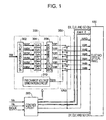
- FIG. 1 is a block diagram showing an overall arrangement of an electro-optical device according to an embodiment of the present invention.
- the electro-optical device comprises an electro-optical panel 100, a control circuit 200, and a processing circuit 300.
- control circuit 200 generates a timing signal or a clock signal for controlling each unit according to a vertical scanning signal Vs, a horizontal scanning signal Hs, and a dot clock signal DCLK, supplied from a higher level device (not shown).
- the processing circuit 300 comprises an S/P conversion circuit 302, a plurality of D/A converters 304, and an amplification/inversion circuit 306.
- the S/P conversion circuit 302 distributes image data Vid that designate gray level (brightness) of the pixels supplied from the higher level device in a serial manner as a digital value for each pixel in synchronization with the vertical scanning signal Vs, the horizontal scanning signal Hs, and the dot clock signal DCLK, into 6 systems, or channels ch1 to ch6, and extends the image data Vid by six times along a time axis (S/P conversion) to output as image data Vd1d to Vd6d, as shown in Fig. 5. Therefore, when the image data for one pixel is supplied for one period of the dot clock signal DCLX, the extended image data Vd1d to Vd6d are respectively supplied through 6 periods of dot clocks DCLK.
- the serial-parallel conversion (S/P conversion) is performed to extend the time in which the image signals are applied and obtain a sample and hold time and a sufficient charging and discharging time for the sampling switch described below.
- the S/P conversion circuit 302 outputs image data to blacken the pixels, for example, in synchronization with a selection time of the image belonging to a dummy pixel region described below.
- the D/A converters 304 are D/A converters arranged for each channel ch1 to ch6, and the image data Vd1d to Vd6d convert voltages corresponding to the gray scale levels of the respective pixels into analog image signals.
- the amplification/inversion circuit 306 rotates the analog converted image signals rotated clockwise and counterclockwise using the voltage Vc as a basis, and then, amplifies and supplies them as the image signals Vd1 to Vd6 in an appropriate manner.
- the polarity inversion can be performed in various aspects such as those (a) for every scanning line, (b) for every data line, (c) for every pixel, and (d) for every plane (frame)
- an embodiment of the present invention employs a polarity inversion (a) for every scanning line.
- the present invention is not limited hereto.
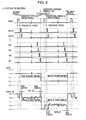
- the voltage Vc is an amplitude center voltage of an image signal, as shown in Fig. 6, and is roughly the same as a voltage LCcom applied to a counter electrode.
- a voltage higher than the amplitude center voltage is referred to as a positive voltage
- a voltage lower than the amplitude center voltage is referred to as a negative voltage, respectively.
- a precharge voltage generation circuit 310 generates a voltage signal Vpre for precharging, for a retrace period immediately prior to sampling the image signals into the data lines.
- a graying voltage gray-like voltage
- Vpre a graying voltage that is an intermediate value between a highest gray scale or white color, and a lowest gray scale or black color is used as a precharge voltage signal Vpre.
- polarity is inverted for every scanning line, so that, in one horizontal scanning period, a positive polarity writing and a negative polarity writing are alternatively performed for every one horizontal scanning period.
- the precharge voltage generation circuit 310 inverts and generates the precharge voltage signal Vpre for every one horizontal scanning period to be a positive gray-like voltage Vg(+) for a retrace period immediately prior to the positive polarity writing, or to be a negative gray-like voltage Vg(-) for a retrace period immediately prior to the negative polarity writing, respectively, as shown in Fig. 6.
- a selector 350 selects the image signals Vd1 to Vd6 by using the amplification/inversion circuit 306 when a signal NRG is an L level, for example, while selecting the precharge voltage signal Vpre by using the precharge voltage generation circuit 310 when a signal NRG is an H level, so that each selected signal is supplied to the electro-optical panel 100 as Vid1 to Vid6.
- the signal NRG is supplied from the control circuit, and is a signal that is in an H level for a precharge period or a portion of a retrace period.
- the signals Vid1 to Vid6 become the precharge voltage signal Vpre in common, for a precharge time where the signal NRG is an H level, and become the image signals Vd1 to Vd6, respectively, for other periods.
- Fig. 2 is a block diagram showing an electrical arrangement of the electro-optical panel 100.
- the electro-optical panel 100 is a liquid crystal panel in which an element substrate and a counter substrate where counter electrodes are provided are attached with a gap therebetween and liquid crystal is sealed into the gap.
- scanning lines 112 are horizontally extended in the drawing, while 1044 (6 x 174) data lines 114 are vertically arranged in the drawing. Further, pixels 110 are arranged at intersections between scanning lines 112 and data lines 114.
- the pixels 110 are arranged in a matrix type of 768 vertical rows and 1044 horizontal columns.
- the leftmost ten columns and the rightmost ten columns in the pixel arrangements that do not attribute to the display are used as dummy pixel regions.
- a display contributing region or an effective pixel region is 768 vertical rows and 1024 horizontal columns corresponding to a region excluding each leftmost and rightmost ten columns.
- an N-channel type TFT (thin film transistor) 116 has a source connected to a data line 114, a drain connected the pixel electrode 118, and a gate connected to the scanning line.
- the counter electrode 108 is commonly arranged for all the pixels to face the pixel electrode 118, and a liquid crystal layer 105 is interposed between the pixel electrode 118 and the counter electrode 108.
- a liquid crystal capacitor comprises the pixel electrode 118, the counter electrode 108, and the liquid crystal layer 105, for each pixel.
- a rubbing processed alignment film is arranged such that a long axis direction of the liquid crystal molecules are consecutively tilted, for example, about 90 degrees between both substrates, while a polarizer is arranged on each opposing side of both substrates, according to the direction of alignment.
- a storage capacitor 109 is arranged for every pixel.
- One end of the storage capacitor 109 is connected to the pixel electrode 118 (drain of the TFT 116), while the other end thereof is commonly grounded through all pixels.
- peripheral circuits such as a scanning line driving circuit 130 or a shift register 140 are arranged around the effective pixel region and the dummy pixel region.
- the scanning line driving circuit 130 supplies scanning signals G1, G2, G3, ⁇ , and G768 that are in an L level only for one horizontal effective display period one after another, to 1st, 2nd, 3rd, ⁇ , and 768th row of the scanning lines, respectively, as shown in Fig. 5.
- the scanning line driving circuit 130 has an arrangement such that a waveform shaping processing is performed, for example, a transmission start pulse DY firstly supplied of one vertical scanning period 1F is shifted one after another each time that a level of a clock signal CLY transits (up or down), and then, reduces a pulse width to output as the scanning signals G1, G2, G3, ⁇ , and G768.
- a waveform shaping processing for example, a transmission start pulse DY firstly supplied of one vertical scanning period 1F is shifted one after another each time that a level of a clock signal CLY transits (up or down), and then, reduces a pulse width to output as the scanning signals G1, G2, G3, ⁇ , and G768.
- the shift register 140 refers to 175 stages of latch circuits 1450 connected in parallel, for transmitting the transmission start pulses DX one after another, according to clock signal CLX having a duty ratio of almost 50%, and a clock signal CLXinv having a logical inversion relationship with the clock signal CLX.
- the transmission start pulse DX is supplied at the start time of one horizontal scanning period, referring to a signal having a pulse width (a period for an H level) of almost one period of the clock signal CLX.
- a shift register 140 has an arrangement such that the transmission start pulse can be transmitted either to the right direction (R direction or clockwise direction) or to the left direction (L direction or counterclockwise direction).
- Signals Dir-R, Dir-L, having logic levels exclusive with each other designate the transmission direction, and a transmission toward the R direction is indicated when the signal Dir-R is an H level (when the signal Dir-L is a L level) while a transmission toward the L direction is indicated when the signal Dir-L is an H level (when the signal Dir-R is a L level).
- the latch circuit 1450 uses a left end as an input and a right end as an output.
- the left 1st stage, left 2nd stage, ⁇ , and left 174th stage, and left 175th stage are represented from the left of the drawing one after another.
- the signals F1, F2, ⁇ , F174 are output from the left 1st stage, left 2nd stage, ⁇ , left 174th stage of the latch circuit 1450, respectively.
- the latch circuit 1450 uses a right end as an input and a left end as an output.
- the right 1st stage, right 2nd stage, ⁇ , and right 174th stage, and right 131st stage are represented from the left of the drawing one after another.
- the signals F174, F173, ⁇ , F1 are output from the right 1st stage, right 2nd stage, ⁇ , right 174th stage of the latch circuit 1450, respectively.
- the left 2nd stage of the latch circuit 1450 is the same as the right 174th stage of the latch circuit 1450, for example. Therefore, according to an embodiment of the present invention, there is no discrimination of an even numbered stage and an odd numbered stage between the R direction transmission (counting from the left) and the L direction transmission (counting from the right).
- a clocked inverter 152 supplies the transmission start pulse DX as an input to the left 1st stage of the latch circuit 1450 only in the R direction transmission where the signal Dir-R is in the H level. Further, a clocked inverter 154 supplies the transmission start pulse DX as an input to the right 1st stage of the latch circuit 1450 only in the R direction transmission where the signal Dir-L is in the H level.
- Fig. 4 is a diagram showing an arrangement comprising three stages, or an odd numbered mth stage of the latch circuit 1450, an even numbered (m+1)th stage of the latch circuit 1450, and an odd numbered (m+2)th stage of the latch circuit 1450.
- Every latch circuit 1450 has four clocked inverters 1451 to 1454.
- the clocked inverter 1451 inverts a logic level of the input signal when the clock signal CLX is in the H level, and makes the output in a high impedance when the clock signal CLX is in the L level
- the clocked inverter 1452 inverts a logic level of the input signal when the clock signal CLXinv is in the H level, and makes the output in a high impedance when the clock signal CLXinv is in the L level.
- the clocked inverter 1453 inverts a logic level of the input signal when the clock signal Dir-R is in the H level, and makes the output in a high impedance when the clock signal Dir-R is in the L level
- the clocked inverter 1454 inverts a logic level of the input signal when the clock signal Dir-L is in the H level, and makes the output in a high impedance when the clock signal Dir-L is in the L level.
- the clocked inverter 1451 inverts a logic level of the input signal when the clock signal CLXinv is in the H level, and makes the output in a high impedance when the clock signal CLXinv is in the L level
- the clocked inverter 1452 inverts a logic level of the input signal when the clock signal CLX is in the H level, and makes the output in a high impedance when the clock signal CLX is in the L level
- the clocked inverters 1453 and 1454 do not have any difference between the odd numbered stage and the even numbered stage.
- the shift register 140 has an arrangement in which the odd numbered stage of the latch circuit 1450 and the even numbered stage of the latch circuit 1450 are alternatively connected.
- the output of the clocked inverter 1454 is in the high impedance throughout all stages, so that it is electrically negligible, while the clocked inverter 1453 is a simple NOT circuit.
- the clocked inverter 1451 inverts a logic level of the input signal from the left end and supplies the logic level to the input stage of the clocked inverter 1453, and the clocked inverter 1453 re-inverts the logical level of the signal supplied to the input stage to supply to input stage of the clocked inverter 1452 along with the output signal from the latch circuit 1450.
- the output of the clocked inverter 1452 for the odd numbered stage becomes a high impedance state.
- the output of the clocked inverter 1453 or the output signal of the odd numbered stage is designated based only on the output level of the clocked inverter 1451.
- the signal Fm output from the odd numbered stage of the latch circuit 1450 is a clockwise rotated signal that repeats twice the logic inversion of the input signal at the left end.
- the clocked inverter 1452 inverts the logic level of the output signal by using the clock inverter 1453 and is fed back to the given clocked inverter 1453.
- the output of the clocked inverter 1451 for the odd numbered stage is in the high impedance.
- the signal Fm output from the odd numbered mth stage of the latch circuit 1450 is a latched one output from the clocked inverter 1453 immediately before the clock signal CLX is in the L level.
- the clock signal CLX is a latched one output from the clocked inverter 1453 immediately before the clock signal CLX is in the H level.
- the signal F(m+1) output from the even numbered (m+1)th stage of the latch circuit 1450 is a half period delayed one of the clock signal CLX (clock signal CLXinv) compared to the signal Fm output from the previous stage, or the odd numbered m stage of the latch circuit 1450.
- the shift register 140 has an arrangement in which these odd numbered stages and even numbered stages of the latch circuit 1450 are alternatively connected.
- the signals F1, F2, F3, ⁇ output from the left 1st stage, left 2nd stage, left 3rd stage, ⁇ will be as shown in Fig. 5.
- the first signal F1 is a signal that rotates the transmission start pulse DX clockwise when the clock signal CLX is in the H level, and a latched one of the immediately previous clockwise rotated output when the clock signal CLX is in the L level.
- the second signal F2 is a signal latched by the left 1st stage of the latch circuit when the clock signal CLX is in the L level, and a latched one of the immediately previous clockwise rotated output when the clock signal CLX is in the H level, and the following signals are repeated in the same manner. Therefore, the signals F1, F2, F3, ⁇ , and F174 are shifted one after another by a half period of the clock signal CLX (clock signal CLXinve).
- the output of the clocked inverter 1453 is in the high impedance throughout all stages, so that it is electrically negligible, while the clocked inverter 1454 is a simple NOT circuit.
- the odd number (m+2)th stage of the latch circuit 1450 when the clock signal CLX is in the L level, the clocked inverter 1452 inverts the logic level of the signal input from the right end to supply to the input stage of the clocked inverter 1454, and the clocked inverter 1454 re-inverts the logic level of the signal supplied to the input stage to supply to the input stage of the clocked inverter 1451 where the output is in the high impedance, as well as to output as a signal F(m+1). Therefore, in the L direction transmission, the signal F(m+1) output when the clock CLK is in the L level becomes a clockwise rotated signal that twice rotates the logical inversion of the input signal at the right end.
- the clocked inverter 1451 Inverts the logic level of the signal output by the clock inverter 1454 to feed back to the given clocked inverter 1454. Therefore, in the L direction transmission, the signal F(m+1) output when the clock signal CLX is in the H level is a latched one output from the odd numbered (m+2) stage of the clocked inverter 1454 immediately before the clock signal CLX is in the H level.
- the signal Fm output from the even numbered (m+1) stage of the latch circuit 1450 is a signal latched by a clockwise rotated signal that repeats twice the logical inversion of the input signal at the right end, or one previous stage of the odd numbered (m+2) stage of the latch circuit 1450.
- the signal Fm output when the clock signal CLX is in the L level is a latched one output from the clocked inverter 1454 of the even numbered (m+1) stage immediately before the clock signal CLX is in the L level.
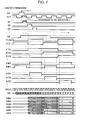
- the signals F174, F173, F172, ⁇ output from the right 1st stage, right 2nd stage, right 3rd stage, ⁇ of the latch circuit 1450 are as shown Fig. 7.
- the first signal F174 is a signal that rotates the transmission start pulse DX clockwise when the clock signal CLX is in the L level, and a latched one of the immediately previous clockwise rotated output when the clock signal CLX is in the H level.
- the second signal F173 is a signal latched by the right 1st stage of the latch circuit when the clock signal CLX is in the H level, and a latched one of the immediately previous clockwise rotated output when the clock signal CLX is in the L level, and the following signals are repeated in the same manner. Therefore, the signals F174, F173, F172, ⁇ , and F1 are shifted one after another by a half period of the clock signal CLX (clock signal CLXinv).
- clocked inverters 1451, 1452, 1453, and 1454 are well known respectively, each of which complementarily comprises two P-channel type TFTs and two N-channel type TFTs connected in serial in a range from the high level voltage to the low level voltage of the power supply.
- the clock signal CLX shown in Fig. 4 as well as the clock signal CLXinv is supplied to the odd numbered stage of the clocked inverter 1451, for example.
- the signal Dir-R shown in Fig. 4 as well as the signal Dir-L not shown is supplied to the clocked inverter 1453.
- each signal path of the output signals F1, F2, ⁇ , F174 by the shift register 140 is branched into two, or the right and left directions in Fig. 2, respectively, and in principle, the operation circuit comprising a NAND circuit 142, a NOT circuit 143, a NAND circuit 144, and NOT circuits 145 and 146 is respectively arranged after each branched path.
- the NAND circuit 142 corresponding to the left-branched path of Fig. 2 outputs a NAND signal referred to as the given signal Fm and the enable signal Enb1, while the NAND circuit 142 corresponding to the right-branched path outputs a NAND signal referred to as the given signal Fm and the enable signal Enb1.
- the NAND circuit 142 corresponding to the left-branched path of Fig. 2 outputs a NAND signal referred to as the given signal F(m+1) and the enable signal Enb3, while the NAND circuit 142 corresponding to the right-branched path outputs a NAND signal referred to as the given signal F(m+1) and the enable signal Enb2.
- enable signals Enb1 and Enb2 are signals supplied from the control circuit 200 (refer to Fig. 1), and phases thereof are shifted by 180 degrees with each other, as shown in Fig. 5. Further, the pulse width of the enable signal Enb1 at a H level is smaller than that of the clock signal CLX at the H level by a predetermined dimension at the front and rear ends of the clock signal CLX at the H level, and the pulse width of the enable signal Enb2 at an L level is smaller than that of the clock signal CLX at the L level by a predetermined dimension at the front and rear ends of the clock signal CLX at the L level.
- the NAND circuit 144 outputs a NAND operated signal between a signal NAND operated by the NAND circuit 142 and a signal inverted from the signal NRZ by the NOT circuit 143.
- the NOR operated signal by the NOR circuit 144 is output as a sampling signal through even times (twice in Fig. 2) of logical inversion by the NOT circuits 145 and 146.
- the sampling signals of which original signals are respectively signals F1, F2, ⁇ , and F174 are referred to as S1, S2, ⁇ , and S174.
- the reason why the NAND circuit 144 performs a NAND operation using NOT circuits 145 and 146 is that it is necessary to branch the signals into 6 and supply the branched signals to a gate of the TFT as a sampling switch 148, with a high driving capacity. For this reason, the size of the transistor is gradually increased to the NOT circuit 145 and 146.
- the sampling switch 148 is, for example, an N-channel type TFT, for sampling into the data lines 114 the respective signals Vid1 to Vid6 of six channels supplied through six image signal lines 171 arranged for every data line 114.
- the source is connected to the image signal line 171 to which the signal Vid1 is supplied.
- the source is connected to the image signal line 171 to which the signal Vid2 to Vid6 is supplied.
- the source of the sampling switching in which a drain is connected to the eleventh data line 114 counting from the left side of Fig. 2 is connected to the image signal line 171 to which the signal Vid5 is supplied since the remainder that divides '11' into 6 is '5'.
- each sampling signal S(i+1) is commonly supplied to the gate of 6 sampling switches 148 connected to the drain.
- (j-1) is '6' to '11'
- the quotient that divides the resultant number into 6 is '1' so that the sampling signal S2 is commonly supplied to the gate of the sampling switch 148 corresponding to these data lines 114.
- six data lines 114 having a relation that the same sampling signal is supplied to the gate of the corresponding sampling switch 148 are regarded as a block.
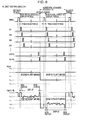
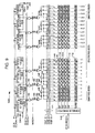
- FIGs. 5 and 6 are timing charts for illustrating operation of an electro-optical device in the R direction transmission.
- a transmission start pulse DY is supplied to a scanning line driving circuit 130.
- the scanning signals G1, G2, G3, ⁇ , and G768 are in the H level exclusively only for the horizontal effective display period, as shown in Fig. 5.
- the precharge voltage generation circuit 310 makes a precharge voltage signal Vpre a voltage Vg(+) corresponding to the positive polarity writing.
- a selector 350 selects the precharge voltage signal Vpre, so that six image signal lines 171 is a voltage Vg(+) corresponding to the positive polarity writing for the immediately following horizontal effective display period.
- the NAND signal by the NAND circuit 144 is forced to be the H level, so that all sampling switches 148 are turned on. Therefore, when the signal NRG is in the H level, the voltage signal Vpre of the image signal line 171 is sampled so that all of the data lines 114 are precharged into Vg(+) as the pre-established positive polarity writing.
- the NAND circuit 144 acts as a NOT circuit for inverting a logic level of the NAND signal by the NAND circuit 142.
- the transmission start pulse DX is shifted one after another by each latch circuit 1450 of the shift register 140, and output as the signals F1, F2, F3, ⁇ through a horizontal effective display period.
- the odd numbered m signal Fm may reduce a pulse width by performing NAND operation of the enable signal Enb1 with the NAND circuit 142, and further, is output as the sampling signal Sm through the NAND circuit 144, and the NOT circuits 145 and 146.
- the even numbered (m+1) signal F(m+1) can reduce a pulse width by performing NAND operation of the enable signal Enb2 with the NAND circuit 142, and further, is output as the sampling signal F(m+1) through the NOT circuit 145 and 146.
- the image data Vid supplied in synchronization with the horizontal period are distributed into six channels by the S/P conversion circuit 302, and extended by six times along the time axis, and secondly, converted into each analog signal by the D/A converters 304, and outputs as a basis of the voltage Vc corresponding to the positive polarity writing.
- the clockwise rotated image signals Vd1 to Vd6 are in the High level voltage compared to the voltage Vc as the pixels are used as black ones.
- a signal NRG is the L level.
- a selector 350 selects the given image signals Vd1 to Vd6, so that the signals Vid1 to Vid6 supplied to six image signal lines 171 become image signals Vd1 to Vd6 by the amplification/inversion circuit 306.
- a voltage variation of the signal Vid1 corresponding to the channel ch1 is shown.
- the signal Vid1 supplied to the image signal line 171 is some portion of the black-like voltage
- the precharge voltage signal Vpre is provided so that the signal is in gray-like voltages Vg(+) or Vg(-) corresponding to the immediately following writing polarity.
- image signals Vd1 to Vd6 are respectively sampled for each of the 1st to 6th data lines 114 counting from the left side of Fig. 2. Further, the sampled image signals Vd1 to Vd6 are respectively applied to the pixel electrode 118 of the pixel 110 corresponding to the intersections of the 1st to 6th data lines 114 and the 1st scanning line 112 counting from the upper portion of Fig. 2.
- the first to sixth data lines 114 belong to the dummy pixel region, so that the sampled image signals are black-like voltage Vb(+) in response to the positive polarity writing. For this reason, pixels in a range of 1st row ⁇ 1st column to 1st row ⁇ 6th column perform a black display.
- each image signal Vd1 to Vd6 is sampled.
- the sampled image signals are respectively applied to the pixel electrode 118 of the pixel 110 corresponding to the intersection between the first row scanning line 112 and the seventh to twelfth data lines 114.
- the seventh to twelfth data lines 114 belong to the dummy pixel regions, so that the sampled image signals are in the black-like voltage Vb(+) identical to the 1st to 6th data lines. For this reason, pixels in the range of 1st row ⁇ 7th column to 1st row ⁇ 10th column are blackened.
- the eleventh and twelfth data lines 114 belong to the effective pixel region and the sampled image signals are gray scale levels indicated by the image data Vid, corresponding to the positive polarity writing. For this reason, the pixels in a range of 1st row ⁇ 11th column to 1st row ⁇ 12th column are in gray levels indicated by the image data Vid.
- the effective pixel that contributes to the display starts from the eleventh one.
- each image signal Vd1 to Vd6 is sampled.
- the sampled image signals Vd1 to Vd4 are respectively applied to the pixel electrode 118 of the pixel 110 corresponding to the intersection between the first row scanning line 112 and the thirteenth to eighteenth data lines 114.
- the pixels in a range of 1st row ⁇ 13th column to 1st row ⁇ 18th column are in gray levels indicated by the image data Vid.
- the 1035th to 1038th data lines belong to the dummy pixel region so that the sampled image signals are in the black-like voltage Vb(+). For this reason, pixels in a range of 1st row x 1035th column to 1st row x 1038th column are blackened.
- the sampling signal S174 is in the H level
- the 1039th to 1044th data lines 114 belong to the dummy pixel regions, the sampled image signals are in the black-like voltage Vb(+). For this reason, pixels in the range of 1st row x 1039th column to 1st row x 1044th column are blackened.
- the pixel that contributes to the display is completed at the 1034th one.
- the range of effective pixels contributing the display is from 11th to 1034th, or 1024 columns.
- the scanning signal G1 becomes to the L level.
- the TFT 116 connected to the first row scanning line 112 turns off, but due to the storage capacitor 109 and capacitance of the liquid crystal layer itself, the pixel electrode 118 is retained to the voltage written at the time of 'on' so that the gray scale corresponding to the given retention voltage is retained.
- the amplification/inversion circuit 306 inverts the analog signal by the D/A converters 304 as a basis of the voltage Vc in response to each negative polarity writing, so that the signals Vid1 to Vid6 (Vd1 to Vd6) correspond to the voltage lower than a voltage Vc, as the pixels are blackened (see Fig. 6).
- the scanning signals G3, G4, ⁇ , and G768 are in the H level and writing is performed on the pixels in the 3rd row, 4th row, ⁇ , 768th.
- the positive polarity writing for the pixels in the odd numbered rows, and the negative polarity writing for the pixels in the even numbered rows are performed, and for this one vertical scanning period, writing into the 1st to 768th rows of pixels is completed.
- the same writing is performed, but at this time, a writing polarity for each row of pixel can be interchanged.
- the negative polarity writing for the pixels in the odd numbered rows, and the positive polarity writing for the pixels in the even numbered rows are performed.
- the precharge voltage signal Vpre is also polarity-inverted.
- a difference compared to the R direction transmission is that the sampling signals S174, S173, S172, ⁇ , and S1 are in the H level one after another, and the distribution sequence of the image signals Vd1 to Vd6 to the image signal line 171 is reversed as the sampling switch 148 and the image signal line 171 are in the block to be fixedly connected.
- a phase relation between the clock signals CLX and CLXinv and the enable signals Enb1 and Enb2 is also reversed, but this may be coped by interchanging the signal supply path.
- an effective pixel range that contributes to the display is restricted to the 11th to 1034th pixels, or 1024 pixels in total.
- the restriction herein will be described below.
- the first half of the positive pulse (H level) in the signal F1 output at first from the shift register 140 is one clockwise rotating the transmission start pulse DX clockwise for a period when the clock signal CLX is in the H level, while the first halves of the positive pulses in the signals F2, F3, ⁇ , and F174 are respectively obtained by normally outputting the signals latched by the latch circuits at the previous stages.
- the signal F1 to be the first positive pulse since the signal F1 to be the first positive pulse does not have a latch circuit at the previous stage, the signal F1 is output under different condition and in waveform from those of other signals F2, F3, ⁇ , and F174.
- the signal F1 can reduce the pulse width by NAND operation of the enable signal Enb1, and through repetition, it is output as a sampling signal S1.
- a ranged to be reduced is a former part of the pulse width having different conditions with other signals F2 and F3.
- a conditional state for sampling the image signal into the data line 114 according to the sampling signal S1 based on the signal F1 is different from a conditional stage for sampling the image signal 114 into the data line 114 according to the sampling signals S2, S3, ⁇ , and S174 based on the signal F2.
- the difference of the display quality is noticeable.
- the counter electrode 108 due to a capacitive coupling between the image signal line 171 and the counter electrode 108, a capacitive coupling between the data line 114 and the counter electrode 108, and resistance of the counter electrode 108, the counter electrode 108 to be constant to the voltage LCcom may varies according to the voltage variation of the image signal line 171.
- the image signals are sampled into the data line 114 in the sequence of 1st to 6th, 7th to 12th, and 13th to 18th columns, but for example, due to the voltage variation of the image signal line 171 when the 1st to 6th data lines 114 are selected or the voltage variation of the data line 114 accompanied with the sampling of the image signal, the voltage of the counter electrode 108 may be changed.
- the counter electrode 108 is not in the voltage LCcom even if the image signal is properly applied to the pixel electrode 118 of the corresponding pixel. Therefore, the voltage retained in the liquid crystal capacitor does not become the predetermined value. This is also applicable to each group after a group of 13th to 18th data lines where the image signals are simultaneously sampled.
- an arrangement is provided in which the image signals are sampled into the 6 columns of data lines 114 at the same time, so that it will be appreciated that a unit for representing the display difference is 6 columns, which is noticeable.
- the pixel regions of the 1st to 6th data lines are blackened as the dummy pixel regions that do not contribute to the display. For this reason, the degradation of the display quality is suppressed in advance due to a fact that the signal F1 firstly output in one horizontal scanning period is different from other signals F2, ⁇ , and that the voltage of the counter electrode is changed.
- the first half of the positive pulse (H level) in the signal F174 output at first from the shift register 140 is obtained by normally outputting the transmission start pulse DX as it is for a period when the clock signal CLX is in the L level, while the first halves of the positive pulses in the signals F173, F172, ⁇ , and F1 are respectively obtained by normally outputting the signals latched by the latch circuit at the previous stage.
- the pixel regions of the 1044th to 1039th data lines are blackened as the dummy pixel regions that do not contribute to the display. Therefore, the degradation of the display quality is suppressed in advance.
- the degradation of the display quality results from signals output at first from the shift register 140 for the one horizontal scanning period and a voltage variation of the counter electrode, in the case of the R direction transmission, it will be appreciated that only the region corresponding to the 1st to 6th data lines is designated to be the dummy pixel region so the pixel region of the 1039th to 1044th data lines at the opposite side are not necessarily used as the dummy pixel region.
- the region corresponding to the 1044th to 1039th data lines is designated to be the dummy pixel region so the pixel region of the 6th to 1st data lines are not necessarily used as the dummy pixel region.
- the pixel region of the 1039th to 1044th data lines is used as the dummy pixel region, and in the L direction transmission, the pixel region of the 6th to 1st data lines is used as the dummy pixel region to obtain the left and right symmetry of the image formed in the panel, in the L direction transmission.
- the pixel region may be used as the effective pixel region.
- the pixel region of the 6th to 1st data lines it is possible to use the pixel region of the 6th to 1st data lines as the effective pixel region to contribute to the display.
- the number of data lines 114 for sampling the image signals with the same sampling signals is '6'
- the number of pixels in the horizontal direction '1024' is not divisible, but there is a remainder of '4'.
- the remainder of '4' is located in the effective pixel region by distributing two '2' at the right and left sides thereof, for symmetry.
- the pixel regions corresponding to the 7th to 10th data lines 114 as well as the 1st to 6th data lines and the pixel regions corresponding to the 1035th to 1038th data lines 114 as well as the 1039 to 1044th data lines are used as the dummy pixel regions.
- the pixel regions corresponding to the 7th to 10th and 1035th to 1038th data lines 114 are adjacent to the 1st to 6th and 1039th to 1044th data lines 114 in which the difference of the display quality may easily occur, so that it will be appreciated that the display may be effected by a capacitive coupling between these data lines and pixels.
- the pixel regions corresponding to the 7th to 10th data lines 114 act as a buffer between the effective pixel regions and the 1st to 6th data lines in which the difference of the display quality may easily occur.
- the pixel regions corresponding to the 1035th to 1038th data lines 114 act as a buffer between the effective pixel regions and the 1039th to 1044th data lines in which the difference of the display quality may easily occur.
- the number of the data lines 114 in the effective pixel region is a multiple number of the number of the sampling switches 148 turned on and off at the same, time
- examples of the non-display can be various types other than this.
- the pixel of the dummy pixel region is not the minimum gray scale, and may also be a color close to this, and may be a gray and a black color, or the maximum brightness.
- the pixel 110 may not be partially or fully formed.
- the data line 114 may be omitted.
- the pixel 110 in the dummy pixel region and the pixel 110 in the effective pixel region are the same from a need of preparing a degree of the capacitive coupling at the dummy pixel region and the effective pixel region.
- a light blocking layer (or liquid crystal) may be arranged corresponding to the portion as the dummy pixel region.
- pixels of the dummy pixel region may be discriminated from the pixels of the effective display region.
- the number of channels is not limited to '6', and it may be '2'.
- an arrangement in which the number of pixels in the horizontal direction specified by the display format is divisible, in other words, an arrangement in which the number of the data lines 114 of the effective pixel regions is a multiple number of the number of the sampling switch 148 turned on and off at the same time may be provided.
- processing circuit 300 processes digital image signals Vid, it may also process analog image signals.
- processing circuit 300 has an arrangement of S/P conversion followed by an analog conversion, but it may be an arrangement of the S/P conversion expansion followed by an analog conversion provided that the final result is the same analog signal.
- a TN type liquid crystal a bi-stable type liquid crystal having a memory characteristic such as ferroelectric liquid crystal and a BTN (Bi-stable twisted nematic) liquid crystal, a polymer dispersion type liquid crystal, or a GH (guest-host) type liquid crystal in which a dye (guest) having anisotropic due to absorption of visible light in a long axis direction and a short axis direction are resolved into a liquid crystal (host) of the constant molecular arrangement and the dye molecules are arranged in parallel with the liquid crystal molecules can be used.
- a TN type liquid crystal a bi-stable type liquid crystal having a memory characteristic such as ferroelectric liquid crystal and a BTN (Bi-stable twisted nematic) liquid crystal, a polymer dispersion type liquid crystal, or a GH (guest-host) type liquid crystal in which a dye (guest) having anisotropic due to absorption of visible light in a long axis direction and a
- a vertical alignment may be provided such that the liquid crystal molecules are vertically arranged with respect to both substrates when the voltage is not applied, while the liquid crystal molecules are horizontally arranged with respect to both substrates when the voltage is applied.
- a parallel (horizontal) alignment may also be available such that the liquid crystal molecules are vertically arranged with respect to both substrates when the voltage is applied, while the liquid crystal molecules are horizontally arranged with respect to both substrates when the voltage is not applied.
- liquid crystal and alignment scheme may be applicable to various types.
- the present invention has an arrangement such that the video data (video signal) is S/P expanded to supply across the image signal line, for example, it can be applied to a device such as an electronic luminescent device, an electron emission device, a electrophoretic device, a digital mirror device, and a plasma display.
- a device such as an electronic luminescent device, an electron emission device, a electrophoretic device, a digital mirror device, and a plasma display.
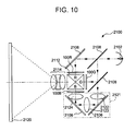
- Fig. 10 is a plan view showing an arrangement of the projector.
- a lamp unit 2102 having a white color light source such as a halogen lamp is arranged inside the projector 2100.
- Projection light emitted from the lamp unit 2102 are divided into the three primary colors R (red), G (green), and B (blue) by three mirrors 2106 and two dichroic mirrors 2108 arranged inside the projector 2100, and then is induced to light valves 100R, 100G, and 100B respectively corresponding to each primary color.
- a relay lens system comprising an incident lens 2122, a relay lens 2123, and an exit lens 2124 are induced to the optical path of the B light component, causing to prevent optical loss.
- the arrangements of the light valves 100R, 100G, and 100B have the same as that of the electro-optical panel 100 according to the embodiments described above, and are respectively driven by image signals corresponding to each color of R, G, and B supplied from a processing circuit (not shown in Fig. 10).
- Light demodulated by the light valves 100R, 100G, and 100B, respectively, is incident into a dichroic prism from 3 directions. Further, in the dichroic prism 2112, the R light component and the B light component are refracted at 90 degrees, while the G light component propagates straight. Therefore, after each color image is combined, a color image is projected to the screen 2120 through a projector lens 2114.
- the light valves 100R, 100G, and 100B since light corresponding to each primary color R, G, and B is incident by the dichroic mirrors 2108, a color filter is not required.
- transmission images of the light valves 100R and 100B are reflected and then transmitted by the dichroic prism 2112, and the transmission image of the light valve 100G is just transmitted.
- the horizontal scanning direction by the light valves 100R and 100B are in the opposite direction to the horizontal scanning direction by the light valve 100G to display the left-right inverted image.
- an electronic apparatus in addition to the example shown in Fig. 10, there can be employed a direct-vision type apparatus such as a mobile telephone, a personal computer, a television, a monitor of a video camera, a car navigation device, a pager, an electronic notebook, a calculator, a word processor, a workstation, a video call, a POS terminal, a digital still camera, and an apparatus having a touch panel.
- a direct-vision type apparatus such as a mobile telephone, a personal computer, a television, a monitor of a video camera, a car navigation device, a pager, an electronic notebook, a calculator, a word processor, a workstation, a video call, a POS terminal, a digital still camera, and an apparatus having a touch panel.
- the electro-optical device according to the present invention can be applied to these various electronic apparatuses.
Landscapes
- Engineering & Computer Science (AREA)
- Physics & Mathematics (AREA)
- Computer Hardware Design (AREA)
- General Physics & Mathematics (AREA)
- Theoretical Computer Science (AREA)
- Chemical & Material Sciences (AREA)
- Crystallography & Structural Chemistry (AREA)
- Control Of Indicators Other Than Cathode Ray Tubes (AREA)
- Liquid Crystal Display Device Control (AREA)
- Liquid Crystal (AREA)
- Transforming Electric Information Into Light Information (AREA)
Applications Claiming Priority (2)
| Application Number | Priority Date | Filing Date | Title |
|---|---|---|---|
| JP2004081518 | 2004-03-19 | ||
| JP2004081518A JP4759925B2 (ja) | 2004-03-19 | 2004-03-19 | 電気光学装置および電子機器 |
Publications (3)
| Publication Number | Publication Date |
|---|---|
| EP1580723A2 true EP1580723A2 (de) | 2005-09-28 |
| EP1580723A3 EP1580723A3 (de) | 2007-01-10 |
| EP1580723B1 EP1580723B1 (de) | 2014-03-19 |
Family
ID=34858356
Family Applications (1)
| Application Number | Title | Priority Date | Filing Date |
|---|---|---|---|
| EP05250819.9A Ceased EP1580723B1 (de) | 2004-03-19 | 2005-02-11 | Elektrooptische Anzeigevorrichtung und elektronisches Gerät mit einer solchen Vorrichtung |
Country Status (5)
| Country | Link |
|---|---|
| US (1) | US7932885B2 (de) |
| EP (1) | EP1580723B1 (de) |
| JP (1) | JP4759925B2 (de) |
| KR (1) | KR100684097B1 (de) |
| CN (1) | CN100432760C (de) |
Families Citing this family (17)
| Publication number | Priority date | Publication date | Assignee | Title |
|---|---|---|---|---|
| JP4691890B2 (ja) * | 2004-03-19 | 2011-06-01 | セイコーエプソン株式会社 | 電気光学装置および電子機器 |
| KR101277975B1 (ko) * | 2006-09-07 | 2013-06-27 | 엘지디스플레이 주식회사 | 쉬프트 레지스터 및 이를 구비한 데이터 드라이버,액정표시장치 |
| JP4315184B2 (ja) * | 2006-10-31 | 2009-08-19 | ブラザー工業株式会社 | 画像読取装置 |
| JP4367509B2 (ja) * | 2007-03-14 | 2009-11-18 | エプソンイメージングデバイス株式会社 | 電気光学装置、駆動回路および電子機器 |
| JP5057335B2 (ja) * | 2008-03-24 | 2012-10-24 | 株式会社ジャパンディスプレイウェスト | 表示装置 |
| JP5165782B2 (ja) * | 2011-08-11 | 2013-03-21 | 株式会社コナミデジタルエンタテインメント | 画像ファイル処理装置およびプログラム |
| KR20150108994A (ko) * | 2014-03-18 | 2015-10-01 | 삼성디스플레이 주식회사 | 표시 장치 및 그 구동 방법 |
| CN104064144B (zh) * | 2014-06-13 | 2016-03-09 | 北京京东方视讯科技有限公司 | 一种显示面板的显示控制电路、显示装置及显示控制方法 |
| JP6551150B2 (ja) * | 2015-10-23 | 2019-07-31 | 株式会社リコー | 画像処理装置、画像形成装置、及び画像処理方法 |
| JP2017129781A (ja) * | 2016-01-21 | 2017-07-27 | 株式会社メガチップス | 色むら補正装置及び色むら補正方法 |
| CN106057160B (zh) * | 2016-08-09 | 2018-10-16 | 武汉华星光电技术有限公司 | 液晶面板及液晶显示器 |
| CN106205457B (zh) * | 2016-08-29 | 2019-02-22 | 武汉华星光电技术有限公司 | 一种显示面板 |
| CN107967904B (zh) * | 2018-01-02 | 2020-07-31 | 上海天马微电子有限公司 | 扫描驱动电路、显示面板和显示装置 |
| KR102664310B1 (ko) * | 2018-08-31 | 2024-05-09 | 엘지디스플레이 주식회사 | 게이트 구동부와 그를 포함한 표시장치 |
| JP7613066B2 (ja) * | 2020-11-27 | 2025-01-15 | セイコーエプソン株式会社 | 回路装置及び電気光学装置 |
| JP7226470B2 (ja) * | 2021-04-26 | 2023-02-21 | セイコーエプソン株式会社 | 電気光学装置および電子機器 |
| KR20240119709A (ko) * | 2023-01-30 | 2024-08-06 | 엘지디스플레이 주식회사 | 발광표시장치 |
Family Cites Families (35)
| Publication number | Priority date | Publication date | Assignee | Title |
|---|---|---|---|---|
| JP2719224B2 (ja) * | 1990-09-28 | 1998-02-25 | シャープ株式会社 | 表示装置の駆動回路 |
| EP1022604B1 (de) * | 1992-02-27 | 2003-09-03 | Canon Kabushiki Kaisha | Flüssigkristallanzeigevorrichtung |
| JPH07175454A (ja) * | 1993-10-25 | 1995-07-14 | Toshiba Corp | 表示制御装置および表示制御方法 |
| JP3246194B2 (ja) * | 1994-06-10 | 2002-01-15 | ソニー株式会社 | アクティブマトリクス型液晶表示装置 |
| DE19540146B4 (de) | 1994-10-27 | 2012-06-21 | Nec Corp. | Flüssigkristallanzeige vom aktiven Matrixtyp mit Treibern für Multimedia-Anwendungen und Ansteuerverfahren dafür |
| JP2625390B2 (ja) | 1994-10-27 | 1997-07-02 | 日本電気株式会社 | 液晶表示装置およびその駆動方法 |
| JP3727416B2 (ja) * | 1996-05-31 | 2005-12-14 | 株式会社半導体エネルギー研究所 | 表示装置 |
| JP3433022B2 (ja) * | 1996-09-20 | 2003-08-04 | 三洋電機株式会社 | 液晶表示装置 |
| JPH10153986A (ja) * | 1996-09-25 | 1998-06-09 | Toshiba Corp | 表示装置 |
| TW455725B (en) * | 1996-11-08 | 2001-09-21 | Seiko Epson Corp | Driver of liquid crystal panel, liquid crystal device, and electronic equipment |
| JPH10149139A (ja) * | 1996-11-18 | 1998-06-02 | Sony Corp | 画像表示装置 |
| EP2189839A1 (de) * | 1997-10-31 | 2010-05-26 | Seiko Epson Corporation | Elektrooptische Vorrichtung und elektronische Vorrichtung |
| JP3694599B2 (ja) | 1997-11-10 | 2005-09-14 | 株式会社 日立ディスプレイズ | 液晶表示装置 |
| TW491954B (en) | 1997-11-10 | 2002-06-21 | Hitachi Device Eng | Liquid crystal display device |
| JP3536653B2 (ja) * | 1998-03-27 | 2004-06-14 | セイコーエプソン株式会社 | 電気光学装置のデータ線駆動回路、電気光学装置、及び電子機器 |
| JP3791208B2 (ja) | 1998-10-01 | 2006-06-28 | セイコーエプソン株式会社 | 電気光学装置の駆動回路 |
| JP3663943B2 (ja) * | 1998-12-04 | 2005-06-22 | セイコーエプソン株式会社 | 電気光学装置および電子機器 |
| JP3635972B2 (ja) * | 1999-02-23 | 2005-04-06 | セイコーエプソン株式会社 | 電気光学装置の駆動回路、電気光学装置および電子機器 |
| TWI245950B (en) * | 1999-03-19 | 2005-12-21 | Sharp Kk | Liquid crystal display apparatus |
| US6909411B1 (en) * | 1999-07-23 | 2005-06-21 | Semiconductor Energy Laboratory Co., Ltd. | Display device and method for operating the same |
| JP4538915B2 (ja) * | 2000-07-24 | 2010-09-08 | セイコーエプソン株式会社 | 電気光学装置の駆動方法 |
| GB2367176A (en) * | 2000-09-14 | 2002-03-27 | Sharp Kk | Active matrix display and display driver |
| JP3744450B2 (ja) * | 2001-05-09 | 2006-02-08 | セイコーエプソン株式会社 | 電気光学装置、駆動用ic及び電子機器 |
| JP3730161B2 (ja) | 2001-11-28 | 2005-12-21 | シャープ株式会社 | 液晶表示装置 |
| US6949883B2 (en) * | 2001-12-06 | 2005-09-27 | Seiko Epson Corporation | Electro-optical device and an electronic apparatus |
| JP2003271108A (ja) * | 2002-03-18 | 2003-09-25 | Hitachi Ltd | 液晶表示装置 |
| JP4190921B2 (ja) | 2002-04-10 | 2008-12-03 | シャープ株式会社 | 駆動回路及びそれを備えた表示装置 |
| JP2004013050A (ja) | 2002-06-11 | 2004-01-15 | Matsushita Electric Ind Co Ltd | 表示装置 |
| JP2004045665A (ja) * | 2002-07-10 | 2004-02-12 | Sharp Corp | データドライバ、表示装置およびその駆動方法 |
| JP2004054058A (ja) | 2002-07-22 | 2004-02-19 | Sharp Corp | 駆動装置及び駆動方法、並びに駆動装置を備えた表示装置 |
| JP2004094058A (ja) * | 2002-09-02 | 2004-03-25 | Semiconductor Energy Lab Co Ltd | 液晶表示装置および液晶表示装置の駆動方法 |
| US7193593B2 (en) * | 2002-09-02 | 2007-03-20 | Semiconductor Energy Laboratory Co., Ltd. | Liquid crystal display device and method of driving a liquid crystal display device |
| TWI273540B (en) * | 2004-02-10 | 2007-02-11 | Sharp Kk | Display apparatus and driver circuit of display apparatus |
| US20050206597A1 (en) * | 2004-02-10 | 2005-09-22 | Seiko Epson Corporation | Electro-optical device, method for driving electro-optical device, driving circuit, and electronic apparatus |
| JP4691890B2 (ja) * | 2004-03-19 | 2011-06-01 | セイコーエプソン株式会社 | 電気光学装置および電子機器 |
-
2004
- 2004-03-19 JP JP2004081518A patent/JP4759925B2/ja not_active Expired - Fee Related
-
2005
- 2005-02-11 EP EP05250819.9A patent/EP1580723B1/de not_active Ceased
- 2005-02-15 US US11/057,852 patent/US7932885B2/en not_active Expired - Fee Related
- 2005-03-11 CN CNB2005100537883A patent/CN100432760C/zh not_active Expired - Fee Related
- 2005-03-19 KR KR1020050022915A patent/KR100684097B1/ko not_active Expired - Fee Related
Non-Patent Citations (1)
| Title |
|---|
| None |
Also Published As
| Publication number | Publication date |
|---|---|
| EP1580723B1 (de) | 2014-03-19 |
| KR20060044453A (ko) | 2006-05-16 |
| US7932885B2 (en) | 2011-04-26 |
| CN1670807A (zh) | 2005-09-21 |
| US20050206969A1 (en) | 2005-09-22 |
| CN100432760C (zh) | 2008-11-12 |
| EP1580723A3 (de) | 2007-01-10 |
| JP2005266577A (ja) | 2005-09-29 |
| JP4759925B2 (ja) | 2011-08-31 |
| KR100684097B1 (ko) | 2007-02-16 |
Similar Documents
| Publication | Publication Date | Title |
|---|---|---|
| KR100707764B1 (ko) | 전기 광학 장치, 그 구동 방법 및 전자 기기 | |
| EP1580723B1 (de) | Elektrooptische Anzeigevorrichtung und elektronisches Gerät mit einer solchen Vorrichtung | |
| JP5332485B2 (ja) | 電気光学装置 | |
| US7358940B2 (en) | Electro-optical device, circuit for driving electro-optical device, method of driving electro-optical device, and electronic apparatus | |
| JP2005165277A (ja) | 輝度ムラの補正方法、輝度ムラの補正回路、電気光学装置および電子機器 | |
| CN101276532B (zh) | 电光装置、其驱动方法以及电子设备 | |
| JP4385730B2 (ja) | 電気光学装置の駆動方法、電気光学装置および電子機器 | |
| US20050206597A1 (en) | Electro-optical device, method for driving electro-optical device, driving circuit, and electronic apparatus | |
| US7495650B2 (en) | Electro-optical device and electronic apparatus | |
| US7602361B2 (en) | Electro-optical device, driving circuit, method, and apparatus to clear residual images between frames and precharge voltage for subsequent operation | |
| US7602359B2 (en) | Image signal correcting method, correcting circuit, electro-optical device, and electronic apparatus | |
| JP4645494B2 (ja) | 電気光学装置、その駆動回路および電子機器 | |
| US7804548B2 (en) | Electro-optical device, method of driving the same, and electronic apparatus | |
| JP2006065212A (ja) | 電気光学装置および電子機器 | |
| JP2007148348A (ja) | 電気光学装置、その駆動方法および電子機器 | |
| JP2007017564A (ja) | 電気光学装置、駆動方法および電子機器 | |
| JP2006195387A (ja) | 電気光学装置および電子機器 | |
| JP2006276119A (ja) | データ信号供給回路、供給方法、電気光学装置および電子機器 | |
| JP2005227391A (ja) | 電気光学装置の駆動回路、駆動方法、電気光学装置および電子機器 | |
| JP2006330510A (ja) | 電気光学装置、駆動方法および電子機器 | |
| JP2006267358A (ja) | 電気光学装置および電子機器 | |
| JP2005321649A (ja) | 電気光学装置、電気光学装置の駆動回路、電気光学装置の駆動方法および電子機器 |
Legal Events
| Date | Code | Title | Description |
|---|---|---|---|
| PUAI | Public reference made under article 153(3) epc to a published international application that has entered the european phase |
Free format text: ORIGINAL CODE: 0009012 |
|
| AK | Designated contracting states |
Kind code of ref document: A2 Designated state(s): AT BE BG CH CY CZ DE DK EE ES FI FR GB GR HU IE IS IT LI LT LU MC NL PL PT RO SE SI SK TR |
|
| AX | Request for extension of the european patent |
Extension state: AL BA HR LV MK YU |
|
| PUAL | Search report despatched |
Free format text: ORIGINAL CODE: 0009013 |
|
| AK | Designated contracting states |
Kind code of ref document: A3 Designated state(s): AT BE BG CH CY CZ DE DK EE ES FI FR GB GR HU IE IS IT LI LT LU MC NL PL PT RO SE SI SK TR |
|
| AX | Request for extension of the european patent |
Extension state: AL BA HR LV MK YU |
|
| 17P | Request for examination filed |
Effective date: 20070605 |
|
| AKX | Designation fees paid |
Designated state(s): DE FR GB |
|
| 17Q | First examination report despatched |
Effective date: 20071102 |
|
| GRAP | Despatch of communication of intention to grant a patent |
Free format text: ORIGINAL CODE: EPIDOSNIGR1 |
|
| INTG | Intention to grant announced |
Effective date: 20131018 |
|
| GRAS | Grant fee paid |
Free format text: ORIGINAL CODE: EPIDOSNIGR3 |
|
| GRAA | (expected) grant |
Free format text: ORIGINAL CODE: 0009210 |
|
| AK | Designated contracting states |
Kind code of ref document: B1 Designated state(s): DE FR GB |
|
| REG | Reference to a national code |
Ref country code: GB Ref legal event code: FG4D |
|
| REG | Reference to a national code |
Ref country code: DE Ref legal event code: R096 Ref document number: 602005043001 Country of ref document: DE Effective date: 20140430 |
|
| REG | Reference to a national code |
Ref country code: DE Ref legal event code: R097 Ref document number: 602005043001 Country of ref document: DE |
|
| PLBE | No opposition filed within time limit |
Free format text: ORIGINAL CODE: 0009261 |
|
| STAA | Information on the status of an ep patent application or granted ep patent |
Free format text: STATUS: NO OPPOSITION FILED WITHIN TIME LIMIT |
|
| 26N | No opposition filed |
Effective date: 20141222 |
|
| REG | Reference to a national code |
Ref country code: DE Ref legal event code: R097 Ref document number: 602005043001 Country of ref document: DE Effective date: 20141222 |
|
| REG | Reference to a national code |
Ref country code: FR Ref legal event code: PLFP Year of fee payment: 12 |
|
| REG | Reference to a national code |
Ref country code: FR Ref legal event code: PLFP Year of fee payment: 13 |
|
| REG | Reference to a national code |
Ref country code: FR Ref legal event code: PLFP Year of fee payment: 14 |
|
| PGFP | Annual fee paid to national office [announced via postgrant information from national office to epo] |
Ref country code: DE Payment date: 20200219 Year of fee payment: 16 Ref country code: GB Payment date: 20200219 Year of fee payment: 16 |
|
| PGFP | Annual fee paid to national office [announced via postgrant information from national office to epo] |
Ref country code: FR Payment date: 20200219 Year of fee payment: 16 |
|
| REG | Reference to a national code |
Ref country code: DE Ref legal event code: R119 Ref document number: 602005043001 Country of ref document: DE |
|
| GBPC | Gb: european patent ceased through non-payment of renewal fee |
Effective date: 20210211 |
|
| PG25 | Lapsed in a contracting state [announced via postgrant information from national office to epo] |
Ref country code: DE Free format text: LAPSE BECAUSE OF NON-PAYMENT OF DUE FEES Effective date: 20210901 Ref country code: GB Free format text: LAPSE BECAUSE OF NON-PAYMENT OF DUE FEES Effective date: 20210211 Ref country code: FR Free format text: LAPSE BECAUSE OF NON-PAYMENT OF DUE FEES Effective date: 20210228 |