EP1559138B1 - Procede de formation d'une zone fragile dans un substrat par co-implantation - Google Patents
Procede de formation d'une zone fragile dans un substrat par co-implantation Download PDFInfo
- Publication number
- EP1559138B1 EP1559138B1 EP03767871A EP03767871A EP1559138B1 EP 1559138 B1 EP1559138 B1 EP 1559138B1 EP 03767871 A EP03767871 A EP 03767871A EP 03767871 A EP03767871 A EP 03767871A EP 1559138 B1 EP1559138 B1 EP 1559138B1
- Authority
- EP
- European Patent Office
- Prior art keywords
- substrate
- species
- fabrication method
- main
- depth
- Prior art date
- Legal status (The legal status is an assumption and is not a legal conclusion. Google has not performed a legal analysis and makes no representation as to the accuracy of the status listed.)
- Expired - Lifetime
Links
- 239000000758 substrate Substances 0.000 title claims abstract description 111
- 238000002513 implantation Methods 0.000 title claims abstract description 56
- 238000000034 method Methods 0.000 title claims abstract description 42
- 238000004519 manufacturing process Methods 0.000 claims abstract description 22
- 239000013626 chemical specie Substances 0.000 claims abstract description 18
- 230000005012 migration Effects 0.000 claims abstract description 8
- 238000013508 migration Methods 0.000 claims abstract description 8
- 238000010438 heat treatment Methods 0.000 claims description 22
- 239000001257 hydrogen Substances 0.000 claims description 16
- 229910052739 hydrogen Inorganic materials 0.000 claims description 16
- 150000002500 ions Chemical class 0.000 claims description 13
- 238000000926 separation method Methods 0.000 claims description 7
- -1 hydrogen ions Chemical class 0.000 claims description 4
- 239000002562 thickening agent Substances 0.000 claims description 3
- 239000012530 fluid Substances 0.000 claims description 2
- 230000003313 weakening effect Effects 0.000 claims description 2
- 238000005452 bending Methods 0.000 claims 1
- 230000000977 initiatory effect Effects 0.000 claims 1
- 238000003780 insertion Methods 0.000 claims 1
- 230000037431 insertion Effects 0.000 claims 1
- 238000004093 laser heating Methods 0.000 claims 1
- 229910052756 noble gas Inorganic materials 0.000 claims 1
- 239000010409 thin film Substances 0.000 abstract description 5
- 239000010410 layer Substances 0.000 description 61
- 230000007547 defect Effects 0.000 description 21
- 125000004429 atom Chemical group 0.000 description 17
- UFHFLCQGNIYNRP-UHFFFAOYSA-N Hydrogen Chemical compound [H][H] UFHFLCQGNIYNRP-UHFFFAOYSA-N 0.000 description 12
- XUIMIQQOPSSXEZ-UHFFFAOYSA-N Silicon Chemical compound [Si] XUIMIQQOPSSXEZ-UHFFFAOYSA-N 0.000 description 12
- 238000012546 transfer Methods 0.000 description 12
- 239000010703 silicon Substances 0.000 description 11
- 229910052710 silicon Inorganic materials 0.000 description 11
- 239000000463 material Substances 0.000 description 9
- 230000008901 benefit Effects 0.000 description 8
- 238000005468 ion implantation Methods 0.000 description 8
- SWQJXJOGLNCZEY-UHFFFAOYSA-N helium atom Chemical compound [He] SWQJXJOGLNCZEY-UHFFFAOYSA-N 0.000 description 7
- 230000008569 process Effects 0.000 description 7
- 239000007789 gas Substances 0.000 description 6
- 230000006870 function Effects 0.000 description 5
- 238000011161 development Methods 0.000 description 4
- VYPSYNLAJGMNEJ-UHFFFAOYSA-N silicon dioxide Inorganic materials O=[Si]=O VYPSYNLAJGMNEJ-UHFFFAOYSA-N 0.000 description 4
- 239000000126 substance Substances 0.000 description 4
- 239000002344 surface layer Substances 0.000 description 4
- 230000000694 effects Effects 0.000 description 3
- 239000001307 helium Substances 0.000 description 3
- 229910052734 helium Inorganic materials 0.000 description 3
- HBMJWWWQQXIZIP-UHFFFAOYSA-N silicon carbide Chemical compound [Si+]#[C-] HBMJWWWQQXIZIP-UHFFFAOYSA-N 0.000 description 3
- 229910010271 silicon carbide Inorganic materials 0.000 description 3
- 238000007669 thermal treatment Methods 0.000 description 3
- 238000011282 treatment Methods 0.000 description 3
- 229910004298 SiO 2 Inorganic materials 0.000 description 2
- 239000003990 capacitor Substances 0.000 description 2
- 239000005350 fused silica glass Substances 0.000 description 2
- 239000011521 glass Substances 0.000 description 2
- 125000004435 hydrogen atom Chemical group [H]* 0.000 description 2
- 230000007246 mechanism Effects 0.000 description 2
- GKAOGPIIYCISHV-UHFFFAOYSA-N neon atom Chemical group [Ne] GKAOGPIIYCISHV-UHFFFAOYSA-N 0.000 description 2
- 230000003647 oxidation Effects 0.000 description 2
- 238000007254 oxidation reaction Methods 0.000 description 2
- JBRZTFJDHDCESZ-UHFFFAOYSA-N AsGa Chemical compound [As]#[Ga] JBRZTFJDHDCESZ-UHFFFAOYSA-N 0.000 description 1
- 229910017214 AsGa Inorganic materials 0.000 description 1
- GPXJNWSHGFTCBW-UHFFFAOYSA-N Indium phosphide Chemical compound [In]#P GPXJNWSHGFTCBW-UHFFFAOYSA-N 0.000 description 1
- 229910013641 LiNbO 3 Inorganic materials 0.000 description 1
- 239000000853 adhesive Substances 0.000 description 1
- 230000001070 adhesive effect Effects 0.000 description 1
- 238000000137 annealing Methods 0.000 description 1
- 230000015572 biosynthetic process Effects 0.000 description 1
- 239000013078 crystal Substances 0.000 description 1
- 239000002178 crystalline material Substances 0.000 description 1
- 230000003247 decreasing effect Effects 0.000 description 1
- 238000000151 deposition Methods 0.000 description 1
- 230000008021 deposition Effects 0.000 description 1
- 238000013461 design Methods 0.000 description 1
- 230000001066 destructive effect Effects 0.000 description 1
- 230000009977 dual effect Effects 0.000 description 1
- 238000010292 electrical insulation Methods 0.000 description 1
- 238000004299 exfoliation Methods 0.000 description 1
- 239000010408 film Substances 0.000 description 1
- 229910052732 germanium Inorganic materials 0.000 description 1
- GNPVGFCGXDBREM-UHFFFAOYSA-N germanium atom Chemical compound [Ge] GNPVGFCGXDBREM-UHFFFAOYSA-N 0.000 description 1
- 239000003292 glue Substances 0.000 description 1
- 230000017525 heat dissipation Effects 0.000 description 1
- 239000007943 implant Substances 0.000 description 1
- 239000012212 insulator Substances 0.000 description 1
- 230000010354 integration Effects 0.000 description 1
- 238000005304 joining Methods 0.000 description 1
- 239000007788 liquid Substances 0.000 description 1
- 238000004943 liquid phase epitaxy Methods 0.000 description 1
- 238000005259 measurement Methods 0.000 description 1
- 230000010070 molecular adhesion Effects 0.000 description 1
- 230000007935 neutral effect Effects 0.000 description 1
- 150000004767 nitrides Chemical class 0.000 description 1
- 230000003287 optical effect Effects 0.000 description 1
- 239000012071 phase Substances 0.000 description 1
- 239000004033 plastic Substances 0.000 description 1
- 238000005498 polishing Methods 0.000 description 1
- 230000001737 promoting effect Effects 0.000 description 1
- 239000010453 quartz Substances 0.000 description 1
- 238000004064 recycling Methods 0.000 description 1
- 230000009467 reduction Effects 0.000 description 1
- 239000010980 sapphire Substances 0.000 description 1
- 229910052594 sapphire Inorganic materials 0.000 description 1
- 230000001629 suppression Effects 0.000 description 1
- 238000002604 ultrasonography Methods 0.000 description 1
Images
Classifications
-
- H—ELECTRICITY
- H01—ELECTRIC ELEMENTS
- H01L—SEMICONDUCTOR DEVICES NOT COVERED BY CLASS H10
- H01L21/00—Processes or apparatus adapted for the manufacture or treatment of semiconductor or solid state devices or of parts thereof
- H01L21/02—Manufacture or treatment of semiconductor devices or of parts thereof
- H01L21/04—Manufacture or treatment of semiconductor devices or of parts thereof the devices having potential barriers, e.g. a PN junction, depletion layer or carrier concentration layer
- H01L21/18—Manufacture or treatment of semiconductor devices or of parts thereof the devices having potential barriers, e.g. a PN junction, depletion layer or carrier concentration layer the devices having semiconductor bodies comprising elements of Group IV of the Periodic Table or AIIIBV compounds with or without impurities, e.g. doping materials
- H01L21/26—Bombardment with radiation
- H01L21/263—Bombardment with radiation with high-energy radiation
- H01L21/265—Bombardment with radiation with high-energy radiation producing ion implantation
- H01L21/26506—Bombardment with radiation with high-energy radiation producing ion implantation in group IV semiconductors
-
- H—ELECTRICITY
- H01—ELECTRIC ELEMENTS
- H01L—SEMICONDUCTOR DEVICES NOT COVERED BY CLASS H10
- H01L21/00—Processes or apparatus adapted for the manufacture or treatment of semiconductor or solid state devices or of parts thereof
- H01L21/02—Manufacture or treatment of semiconductor devices or of parts thereof
- H01L21/04—Manufacture or treatment of semiconductor devices or of parts thereof the devices having potential barriers, e.g. a PN junction, depletion layer or carrier concentration layer
- H01L21/18—Manufacture or treatment of semiconductor devices or of parts thereof the devices having potential barriers, e.g. a PN junction, depletion layer or carrier concentration layer the devices having semiconductor bodies comprising elements of Group IV of the Periodic Table or AIIIBV compounds with or without impurities, e.g. doping materials
- H01L21/26—Bombardment with radiation
- H01L21/263—Bombardment with radiation with high-energy radiation
- H01L21/265—Bombardment with radiation with high-energy radiation producing ion implantation
-
- H—ELECTRICITY
- H01—ELECTRIC ELEMENTS
- H01L—SEMICONDUCTOR DEVICES NOT COVERED BY CLASS H10
- H01L21/00—Processes or apparatus adapted for the manufacture or treatment of semiconductor or solid state devices or of parts thereof
- H01L21/70—Manufacture or treatment of devices consisting of a plurality of solid state components formed in or on a common substrate or of parts thereof; Manufacture of integrated circuit devices or of parts thereof
- H01L21/71—Manufacture of specific parts of devices defined in group H01L21/70
- H01L21/76—Making of isolation regions between components
- H01L21/762—Dielectric regions, e.g. EPIC dielectric isolation, LOCOS; Trench refilling techniques, SOI technology, use of channel stoppers
- H01L21/7624—Dielectric regions, e.g. EPIC dielectric isolation, LOCOS; Trench refilling techniques, SOI technology, use of channel stoppers using semiconductor on insulator [SOI] technology
- H01L21/76251—Dielectric regions, e.g. EPIC dielectric isolation, LOCOS; Trench refilling techniques, SOI technology, use of channel stoppers using semiconductor on insulator [SOI] technology using bonding techniques
- H01L21/76254—Dielectric regions, e.g. EPIC dielectric isolation, LOCOS; Trench refilling techniques, SOI technology, use of channel stoppers using semiconductor on insulator [SOI] technology using bonding techniques with separation/delamination along an ion implanted layer, e.g. Smart-cut, Unibond
Definitions
- the invention relates to the separation of a thin layer on the surface of a "source” substrate, for the purpose, usually, to postpone this thin layer on a "target” substrate.
- the patent application FR-2,681,472 discloses such a method.
- the implanted species create a buried zone weakened by the presence of defects such as micro-cavities, in particular micro-bubbles (of essentially spherical shape, in English “bubbles ”) or "platelets” (in the form of a lens, in English “ platelets ").
- This buried zone delimits with the surface of the source substrate a thin layer which will subsequently be transferred to the target substrate.
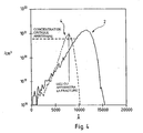
- the secondary concentration in species of lesser effectiveness can be equal to a significant fraction of the concentration which would be sufficient for the subsequent fracture of the substrate at the level of this secondary implantation (it will naturally be necessary to preserve, by choosing this secondary concentration, a certain margin of safety to prevent the substrate from fracturing at this level).
- the secondary species has, according to the invention, a lower efficiency than the main species, it means in practice that the secondary concentration can be significantly higher than the main concentration.
- the three concentration curves rise above this critical concentration, so that, for each concentration curve, we deduce the existence of a disturbed zone in the substrate (zone with crystalline defects having origin ion implantation) located essentially between the two depth levels where said curve intersects the critical concentration line.
- a heat treatment furnace, and / or local heating, and / or laser beam, or other
- mechanical stresses such as the projecting a fluid jet (gas, liquid) and / or inserting a blade at the weakened zone, and / or tensile, shear or flexural stresses applied to the substrate, and / or acoustic waves (ultrasound, or other).
- the rest of the embrittled substrate can be recycled both as a source substrate and as, if appropriate, as a target substrate.
Landscapes
- Physics & Mathematics (AREA)
- Engineering & Computer Science (AREA)
- High Energy & Nuclear Physics (AREA)
- Condensed Matter Physics & Semiconductors (AREA)
- General Physics & Mathematics (AREA)
- Manufacturing & Machinery (AREA)
- Computer Hardware Design (AREA)
- Microelectronics & Electronic Packaging (AREA)
- Power Engineering (AREA)
- Toxicology (AREA)
- Health & Medical Sciences (AREA)
- Crystals, And After-Treatments Of Crystals (AREA)
- Element Separation (AREA)
- Physical Vapour Deposition (AREA)
- Recrystallisation Techniques (AREA)
- Silicon Compounds (AREA)
- Semiconductor Memories (AREA)
- Manufacturing Of Printed Wiring (AREA)
- Laminated Bodies (AREA)
- Moulding By Coating Moulds (AREA)
Applications Claiming Priority (3)
| Application Number | Priority Date | Filing Date | Title |
|---|---|---|---|
| FR0213934A FR2847075B1 (fr) | 2002-11-07 | 2002-11-07 | Procede de formation d'une zone fragile dans un substrat par co-implantation |
| FR0213934 | 2002-11-07 | ||
| PCT/FR2003/003256 WO2004044976A1 (fr) | 2002-11-07 | 2003-10-31 | Procede de formation d'une zone fragile dans un substrat par co-implantation |
Publications (2)
| Publication Number | Publication Date |
|---|---|
| EP1559138A1 EP1559138A1 (fr) | 2005-08-03 |
| EP1559138B1 true EP1559138B1 (fr) | 2010-04-21 |
Family
ID=32116441
Family Applications (1)
| Application Number | Title | Priority Date | Filing Date |
|---|---|---|---|
| EP03767871A Expired - Lifetime EP1559138B1 (fr) | 2002-11-07 | 2003-10-31 | Procede de formation d'une zone fragile dans un substrat par co-implantation |
Country Status (11)
| Country | Link |
|---|---|
| US (1) | US20070037363A1 (ja) |
| EP (1) | EP1559138B1 (ja) |
| JP (2) | JP5258146B2 (ja) |
| KR (2) | KR101174594B1 (ja) |
| CN (1) | CN100587940C (ja) |
| AT (1) | ATE465514T1 (ja) |
| AU (1) | AU2003292305A1 (ja) |
| DE (1) | DE60332261D1 (ja) |
| FR (1) | FR2847075B1 (ja) |
| TW (1) | TWI323912B (ja) |
| WO (1) | WO2004044976A1 (ja) |
Families Citing this family (44)
| Publication number | Priority date | Publication date | Assignee | Title |
|---|---|---|---|---|
| FR2748851B1 (fr) | 1996-05-15 | 1998-08-07 | Commissariat Energie Atomique | Procede de realisation d'une couche mince de materiau semiconducteur |
| FR2773261B1 (fr) | 1997-12-30 | 2000-01-28 | Commissariat Energie Atomique | Procede pour le transfert d'un film mince comportant une etape de creation d'inclusions |
| FR2830983B1 (fr) | 2001-10-11 | 2004-05-14 | Commissariat Energie Atomique | Procede de fabrication de couches minces contenant des microcomposants |
| US7176108B2 (en) | 2002-11-07 | 2007-02-13 | Soitec Silicon On Insulator | Method of detaching a thin film at moderate temperature after co-implantation |
| FR2848336B1 (fr) | 2002-12-09 | 2005-10-28 | Commissariat Energie Atomique | Procede de realisation d'une structure contrainte destinee a etre dissociee |
| FR2856844B1 (fr) | 2003-06-24 | 2006-02-17 | Commissariat Energie Atomique | Circuit integre sur puce de hautes performances |
| FR2861497B1 (fr) | 2003-10-28 | 2006-02-10 | Soitec Silicon On Insulator | Procede de transfert catastrophique d'une couche fine apres co-implantation |
| US7772087B2 (en) | 2003-12-19 | 2010-08-10 | Commissariat A L'energie Atomique | Method of catastrophic transfer of a thin film after co-implantation |
| JP4730581B2 (ja) * | 2004-06-17 | 2011-07-20 | 信越半導体株式会社 | 貼り合わせウェーハの製造方法 |
| WO2006032948A1 (en) * | 2004-09-21 | 2006-03-30 | S.O.I.Tec Silicon On Insulator Technologies | Method for obtaining a thin layer by implementing co-implantation and subsequent implantation |
| FR2886051B1 (fr) | 2005-05-20 | 2007-08-10 | Commissariat Energie Atomique | Procede de detachement d'un film mince |
| FR2889887B1 (fr) | 2005-08-16 | 2007-11-09 | Commissariat Energie Atomique | Procede de report d'une couche mince sur un support |
| DE102005052357A1 (de) | 2005-09-01 | 2007-03-15 | Osram Opto Semiconductors Gmbh | Verfahren zum lateralen Zertrennen eines Halbleiterwafers und optoelektronisches Bauelement |
| FR2891281B1 (fr) | 2005-09-28 | 2007-12-28 | Commissariat Energie Atomique | Procede de fabrication d'un element en couches minces. |
| EP1798764A1 (en) * | 2005-12-14 | 2007-06-20 | STMicroelectronics S.r.l. | Process for manufacturing wafers usable in the semiconductor industry |
| FR2898431B1 (fr) * | 2006-03-13 | 2008-07-25 | Soitec Silicon On Insulator | Procede de fabrication de film mince |
| FR2899378B1 (fr) | 2006-03-29 | 2008-06-27 | Commissariat Energie Atomique | Procede de detachement d'un film mince par fusion de precipites |
| FR2905801B1 (fr) * | 2006-09-12 | 2008-12-05 | Soitec Silicon On Insulator | Procede de transfert d'une couche a haute temperature |
| FR2907965B1 (fr) * | 2006-10-27 | 2009-03-06 | Soitec Silicon On Insulator | Procede de traitement d'un substrat donneur pour la fabrication d'un substrat. |
| FR2910179B1 (fr) | 2006-12-19 | 2009-03-13 | Commissariat Energie Atomique | PROCEDE DE FABRICATION DE COUCHES MINCES DE GaN PAR IMPLANTATION ET RECYCLAGE D'UN SUBSTRAT DE DEPART |
| KR101484296B1 (ko) * | 2007-06-26 | 2015-01-19 | 가부시키가이샤 한도오따이 에네루기 켄큐쇼 | 반도체 기판의 제작방법 |
| FR2922359B1 (fr) * | 2007-10-12 | 2009-12-18 | Commissariat Energie Atomique | Procede de fabrication d'une structure micro-electronique impliquant un collage moleculaire |
| FR2925221B1 (fr) | 2007-12-17 | 2010-02-19 | Commissariat Energie Atomique | Procede de transfert d'une couche mince |
| US8741740B2 (en) * | 2008-10-02 | 2014-06-03 | Semiconductor Energy Laboratory Co., Ltd. | Method for manufacturing SOI substrate |
| US7927975B2 (en) * | 2009-02-04 | 2011-04-19 | Micron Technology, Inc. | Semiconductor material manufacture |
| FR2947098A1 (fr) | 2009-06-18 | 2010-12-24 | Commissariat Energie Atomique | Procede de transfert d'une couche mince sur un substrat cible ayant un coefficient de dilatation thermique different de celui de la couche mince |
| FR2949606B1 (fr) | 2009-08-26 | 2011-10-28 | Commissariat Energie Atomique | Procede de detachement par fracture d'un film mince de silicium mettant en oeuvre une triple implantation |
| US20110207306A1 (en) * | 2010-02-22 | 2011-08-25 | Sarko Cherekdjian | Semiconductor structure made using improved ion implantation process |
| FR2981501B1 (fr) * | 2011-10-17 | 2016-05-13 | Soitec Silicon On Insulator | Procédé de transfert de couches matériau dans des processus d’intégration 3d et structures et dispositifs associes |
| US8673733B2 (en) | 2011-09-27 | 2014-03-18 | Soitec | Methods of transferring layers of material in 3D integration processes and related structures and devices |
| TWI573198B (zh) * | 2011-09-27 | 2017-03-01 | 索泰克公司 | 在三度空間集積製程中轉移材料層之方法及其相關結構與元件 |
| US8841742B2 (en) | 2011-09-27 | 2014-09-23 | Soitec | Low temperature layer transfer process using donor structure with material in recesses in transfer layer, semiconductor structures fabricated using such methods |
| FR2988516B1 (fr) * | 2012-03-23 | 2014-03-07 | Soitec Silicon On Insulator | Procede d'implantation de fragilisation de substrats ameliore |
| US9281233B2 (en) | 2012-12-28 | 2016-03-08 | Sunedison Semiconductor Limited | Method for low temperature layer transfer in the preparation of multilayer semiconductor devices |
| JP2014138152A (ja) * | 2013-01-18 | 2014-07-28 | Fuji Electric Co Ltd | 半導体薄膜フィルムの製造方法 |
| CN104143496B (zh) * | 2013-05-08 | 2016-12-28 | 中国科学院上海高等研究院 | 一种基于层转移的晶硅薄膜的制备方法 |
| WO2015034118A1 (ko) * | 2013-09-09 | 2015-03-12 | Yoo Bong Young | 실리콘 기판의 표면 박리 방법 |
| US10068795B2 (en) | 2014-02-07 | 2018-09-04 | Globalwafers Co., Ltd. | Methods for preparing layered semiconductor structures |
| CN104979425B (zh) * | 2014-04-09 | 2017-03-15 | 中国科学院上海高等研究院 | 一种应用于层转移薄膜生长的籽晶阵列的制备方法 |
| US10546915B2 (en) | 2017-12-26 | 2020-01-28 | International Business Machines Corporation | Buried MIM capacitor structure with landing pads |
| CN112655083A (zh) | 2018-04-27 | 2021-04-13 | 环球晶圆股份有限公司 | 促进从半导体施体衬底的层转移的光辅助薄片形成 |
| WO2019236320A1 (en) | 2018-06-08 | 2019-12-12 | Globalwafers Co., Ltd. | Method for transfer of a thin layer of silicon |
| FR3091620B1 (fr) * | 2019-01-07 | 2021-01-29 | Commissariat Energie Atomique | Procédé de transfert de couche avec réduction localisée d’une capacité à initier une fracture |
| WO2023058355A1 (ja) | 2021-10-06 | 2023-04-13 | 信越半導体株式会社 | ヘテロエピタキシャル膜の作製方法 |
Family Cites Families (54)
| Publication number | Priority date | Publication date | Assignee | Title |
|---|---|---|---|---|
| US4028149A (en) * | 1976-06-30 | 1977-06-07 | Ibm Corporation | Process for forming monocrystalline silicon carbide on silicon substrates |
| DE2849184A1 (de) * | 1978-11-13 | 1980-05-22 | Bbc Brown Boveri & Cie | Verfahren zur herstellung eines scheibenfoermigen silizium-halbleiterbauelementes mit negativer anschraegung |
| US4956698A (en) * | 1987-07-29 | 1990-09-11 | The United States Of America As Represented By The Department Of Commerce | Group III-V compound semiconductor device having p-region formed by Be and Group V ions |
| EP0520294B1 (de) * | 1991-06-24 | 1998-08-26 | Siemens Aktiengesellschaft | Halbleiterbauelement und Verfahren zu seiner Herstellung |
| FR2681472B1 (fr) * | 1991-09-18 | 1993-10-29 | Commissariat Energie Atomique | Procede de fabrication de films minces de materiau semiconducteur. |
| JP3416163B2 (ja) * | 1992-01-31 | 2003-06-16 | キヤノン株式会社 | 半導体基板及びその作製方法 |
| US5424863A (en) * | 1993-09-23 | 1995-06-13 | Ael Industries, Inc. | Dual-polarization fiber optic communications link |
| FR2715501B1 (fr) * | 1994-01-26 | 1996-04-05 | Commissariat Energie Atomique | Procédé de dépôt de lames semiconductrices sur un support. |
| JP3381443B2 (ja) * | 1995-02-02 | 2003-02-24 | ソニー株式会社 | 基体から半導体層を分離する方法、半導体素子の製造方法およびsoi基板の製造方法 |
| CN1132223C (zh) * | 1995-10-06 | 2003-12-24 | 佳能株式会社 | 半导体衬底及其制造方法 |
| FR2744285B1 (fr) * | 1996-01-25 | 1998-03-06 | Commissariat Energie Atomique | Procede de transfert d'une couche mince d'un substrat initial sur un substrat final |
| FR2747506B1 (fr) * | 1996-04-11 | 1998-05-15 | Commissariat Energie Atomique | Procede d'obtention d'un film mince de materiau semiconducteur comprenant notamment des composants electroniques |
| FR2748850B1 (fr) * | 1996-05-15 | 1998-07-24 | Commissariat Energie Atomique | Procede de realisation d'un film mince de materiau solide et applications de ce procede |
| FR2748851B1 (fr) * | 1996-05-15 | 1998-08-07 | Commissariat Energie Atomique | Procede de realisation d'une couche mince de materiau semiconducteur |
| US6127199A (en) * | 1996-11-12 | 2000-10-03 | Seiko Epson Corporation | Manufacturing method of active matrix substrate, active matrix substrate and liquid crystal display device |
| SG65697A1 (en) * | 1996-11-15 | 1999-06-22 | Canon Kk | Process for producing semiconductor article |
| KR100232886B1 (ko) * | 1996-11-23 | 1999-12-01 | 김영환 | Soi 웨이퍼 제조방법 |
| FR2756847B1 (fr) * | 1996-12-09 | 1999-01-08 | Commissariat Energie Atomique | Procede de separation d'au moins deux elements d'une structure en contact entre eux par implantation ionique |
| DE19653831A1 (de) * | 1996-12-21 | 1998-06-25 | Bosch Gmbh Robert | Elektrisches Gerät |
| US6013563A (en) * | 1997-05-12 | 2000-01-11 | Silicon Genesis Corporation | Controlled cleaning process |
| US5877070A (en) * | 1997-05-31 | 1999-03-02 | Max-Planck Society | Method for the transfer of thin layers of monocrystalline material to a desirable substrate |
| US6150239A (en) * | 1997-05-31 | 2000-11-21 | Max Planck Society | Method for the transfer of thin layers monocrystalline material onto a desirable substrate |
| US6534380B1 (en) * | 1997-07-18 | 2003-03-18 | Denso Corporation | Semiconductor substrate and method of manufacturing the same |
| US6103599A (en) * | 1997-07-25 | 2000-08-15 | Silicon Genesis Corporation | Planarizing technique for multilayered substrates |
| FR2767416B1 (fr) * | 1997-08-12 | 1999-10-01 | Commissariat Energie Atomique | Procede de fabrication d'un film mince de materiau solide |
| JP3412470B2 (ja) * | 1997-09-04 | 2003-06-03 | 三菱住友シリコン株式会社 | Soi基板の製造方法 |
| US5920764A (en) * | 1997-09-30 | 1999-07-06 | International Business Machines Corporation | Process for restoring rejected wafers in line for reuse as new |
| JP2998724B2 (ja) * | 1997-11-10 | 2000-01-11 | 日本電気株式会社 | 張り合わせsoi基板の製造方法 |
| FR2773261B1 (fr) * | 1997-12-30 | 2000-01-28 | Commissariat Energie Atomique | Procede pour le transfert d'un film mince comportant une etape de creation d'inclusions |
| US6071795A (en) * | 1998-01-23 | 2000-06-06 | The Regents Of The University Of California | Separation of thin films from transparent substrates by selective optical processing |
| FR2774510B1 (fr) * | 1998-02-02 | 2001-10-26 | Soitec Silicon On Insulator | Procede de traitement de substrats, notamment semi-conducteurs |
| JPH11307747A (ja) * | 1998-04-17 | 1999-11-05 | Nec Corp | Soi基板およびその製造方法 |
| US5909627A (en) * | 1998-05-18 | 1999-06-01 | Philips Electronics North America Corporation | Process for production of thin layers of semiconductor material |
| US6054370A (en) * | 1998-06-30 | 2000-04-25 | Intel Corporation | Method of delaminating a pre-fabricated transistor layer from a substrate for placement on another wafer |
| US6271101B1 (en) * | 1998-07-29 | 2001-08-07 | Semiconductor Energy Laboratory Co., Ltd. | Process for production of SOI substrate and process for production of semiconductor device |
| FR2784795B1 (fr) * | 1998-10-16 | 2000-12-01 | Commissariat Energie Atomique | Structure comportant une couche mince de materiau composee de zones conductrices et de zones isolantes et procede de fabrication d'une telle structure |
| US6346458B1 (en) * | 1998-12-31 | 2002-02-12 | Robert W. Bower | Transposed split of ion cut materials |
| JP4379943B2 (ja) * | 1999-04-07 | 2009-12-09 | 株式会社デンソー | 半導体基板の製造方法および半導体基板製造装置 |
| AU4481100A (en) * | 1999-04-21 | 2000-11-02 | Silicon Genesis Corporation | Treatment method of cleaved film for the manufacture of substrates |
| US6323108B1 (en) * | 1999-07-27 | 2001-11-27 | The United States Of America As Represented By The Secretary Of The Navy | Fabrication ultra-thin bonded semiconductor layers |
| FR2797347B1 (fr) * | 1999-08-04 | 2001-11-23 | Commissariat Energie Atomique | Procede de transfert d'une couche mince comportant une etape de surfragililisation |
| US6263941B1 (en) * | 1999-08-10 | 2001-07-24 | Silicon Genesis Corporation | Nozzle for cleaving substrates |
| JP3975634B2 (ja) * | 2000-01-25 | 2007-09-12 | 信越半導体株式会社 | 半導体ウェハの製作法 |
| WO2001080308A2 (fr) * | 2000-04-14 | 2001-10-25 | S.O.I.Tec Silicon On Insulator Technologies | Procede pour la decoupe d'au moins une couche mince dans un substrat ou lingot, notamment en materiau(x) semi-conducteur(s) |
| FR2809867B1 (fr) * | 2000-05-30 | 2003-10-24 | Commissariat Energie Atomique | Substrat fragilise et procede de fabrication d'un tel substrat |
| US6600173B2 (en) * | 2000-08-30 | 2003-07-29 | Cornell Research Foundation, Inc. | Low temperature semiconductor layering and three-dimensional electronic circuits using the layering |
| FR2818010B1 (fr) * | 2000-12-08 | 2003-09-05 | Commissariat Energie Atomique | Procede de realisation d'une couche mince impliquant l'introduction d'especes gazeuses |
| US6774010B2 (en) * | 2001-01-25 | 2004-08-10 | International Business Machines Corporation | Transferable device-containing layer for silicon-on-insulator applications |
| FR2823373B1 (fr) * | 2001-04-10 | 2005-02-04 | Soitec Silicon On Insulator | Dispositif de coupe de couche d'un substrat, et procede associe |
| US6759282B2 (en) * | 2001-06-12 | 2004-07-06 | International Business Machines Corporation | Method and structure for buried circuits and devices |
| US6593212B1 (en) * | 2001-10-29 | 2003-07-15 | The United States Of America As Represented By The Secretary Of The Navy | Method for making electro-optical devices using a hydrogenion splitting technique |
| FR2834820B1 (fr) * | 2002-01-16 | 2005-03-18 | Procede de clivage de couches d'une tranche de materiau | |
| US6607969B1 (en) * | 2002-03-18 | 2003-08-19 | The United States Of America As Represented By The Secretary Of The Navy | Method for making pyroelectric, electro-optical and decoupling capacitors using thin film transfer and hydrogen ion splitting techniques |
| US6767749B2 (en) * | 2002-04-22 | 2004-07-27 | The United States Of America As Represented By The Secretary Of The Navy | Method for making piezoelectric resonator and surface acoustic wave device using hydrogen implant layer splitting |
-
2002
- 2002-11-07 FR FR0213934A patent/FR2847075B1/fr not_active Expired - Fee Related
-
2003
- 2003-10-31 WO PCT/FR2003/003256 patent/WO2004044976A1/fr active Application Filing
- 2003-10-31 EP EP03767871A patent/EP1559138B1/fr not_active Expired - Lifetime
- 2003-10-31 JP JP2004550719A patent/JP5258146B2/ja not_active Expired - Lifetime
- 2003-10-31 AU AU2003292305A patent/AU2003292305A1/en not_active Abandoned
- 2003-10-31 KR KR1020117007374A patent/KR101174594B1/ko active IP Right Grant
- 2003-10-31 KR KR1020057008062A patent/KR101116540B1/ko active IP Right Grant
- 2003-10-31 CN CN200380102438A patent/CN100587940C/zh not_active Expired - Lifetime
- 2003-10-31 DE DE60332261T patent/DE60332261D1/de not_active Expired - Lifetime
- 2003-10-31 AT AT03767871T patent/ATE465514T1/de not_active IP Right Cessation
- 2003-11-03 TW TW092130631A patent/TWI323912B/zh not_active IP Right Cessation
-
2004
- 2004-05-27 US US10/534,199 patent/US20070037363A1/en not_active Abandoned
-
2011
- 2011-05-18 JP JP2011111487A patent/JP2011223011A/ja active Pending
Also Published As
| Publication number | Publication date |
|---|---|
| CN100587940C (zh) | 2010-02-03 |
| JP2006505941A (ja) | 2006-02-16 |
| JP2011223011A (ja) | 2011-11-04 |
| US20070037363A1 (en) | 2007-02-15 |
| KR20050072793A (ko) | 2005-07-12 |
| TW200414320A (en) | 2004-08-01 |
| JP5258146B2 (ja) | 2013-08-07 |
| TWI323912B (en) | 2010-04-21 |
| KR101174594B1 (ko) | 2012-08-16 |
| DE60332261D1 (de) | 2010-06-02 |
| AU2003292305A1 (en) | 2004-06-03 |
| CN1708844A (zh) | 2005-12-14 |
| KR20110048584A (ko) | 2011-05-11 |
| KR101116540B1 (ko) | 2012-02-28 |
| EP1559138A1 (fr) | 2005-08-03 |
| WO2004044976A1 (fr) | 2004-05-27 |
| FR2847075B1 (fr) | 2005-02-18 |
| FR2847075A1 (fr) | 2004-05-14 |
| ATE465514T1 (de) | 2010-05-15 |
Similar Documents
| Publication | Publication Date | Title |
|---|---|---|
| EP1559138B1 (fr) | Procede de formation d'une zone fragile dans un substrat par co-implantation | |
| EP1285461B1 (fr) | Procede de fabrication d'une couche mince | |
| EP1435111B1 (fr) | Procede de fabrication de couches minces contenant des microcomposants | |
| EP1010198B1 (fr) | Procede de fabrication d'un film mince de materiau solide | |
| EP2102904B1 (fr) | Procede de fabrication de couches minces de gan par implantation et recyclage d'un substrat de depart | |
| EP0963598B1 (fr) | Procede pour le transfert d'un film mince comportant une etape de creation d'inclusions | |
| EP1299905B1 (fr) | Procede de decoupage d'un bloc de materiau et de formation d'un film mince | |
| EP0898307B1 (fr) | Procédé de traitement pour le collage moléculaire et le décollage de deux structures | |
| EP1922752B1 (fr) | Procede de report d'une couche mince sur un support | |
| FR2905801A1 (fr) | Procede de transfert d'une couche a haute temperature | |
| EP1487012A2 (fr) | Procédé de réalisation de structure hétérogène et structure obtenue par un tel procédé | |
| WO2005086227A1 (fr) | Technique d’amelioration de la qualite d’une couche mince prelevee | |
| EP2195835A1 (fr) | Procédé de fabrication d'une structure micro-électronique impliquant un collage moléculaire | |
| WO2005043616A1 (fr) | Procede de transfert catastrophique d'une couche fine apres co-implantation | |
| EP2705529B1 (fr) | Procede de formation d'une fracture dans un materiau | |
| WO2001011667A1 (fr) | Procede de transfert d'une couche mince comportant une etape de surfragilisation | |
| FR2938119A1 (fr) | Procede de detachement de couches semi-conductrices a basse temperature | |
| FR2907966A1 (fr) | Procede de fabrication d'un substrat. | |
| EP1631982B1 (fr) | Procede d'obtention d'une couche tres mince par amincissement par auto-portage provoque | |
| FR2866982A1 (fr) | Procede de fabrication de composants electroniques | |
| FR3059149A1 (fr) | Procede de fabrication d'un film mince a base d'inp ou de gaas |
Legal Events
| Date | Code | Title | Description |
|---|---|---|---|
| PUAI | Public reference made under article 153(3) epc to a published international application that has entered the european phase |
Free format text: ORIGINAL CODE: 0009012 |
|
| 17P | Request for examination filed |
Effective date: 20050525 |
|
| AK | Designated contracting states |
Kind code of ref document: A1 Designated state(s): AT BE BG CH CY CZ DE DK EE ES FI FR GB GR HU IE IT LI LU MC NL PT RO SE SI SK TR |
|
| AX | Request for extension of the european patent |
Extension state: AL LT LV MK |
|
| DAX | Request for extension of the european patent (deleted) | ||
| RIN1 | Information on inventor provided before grant (corrected) |
Inventor name: LAGAHE, CHRISTELLE Inventor name: SOUSBIE, NICOLAS Inventor name: ASPAR, BERNARD Inventor name: MICHAUD, JEAN-FRANCOIS |
|
| 17Q | First examination report despatched |
Effective date: 20080708 |
|
| GRAP | Despatch of communication of intention to grant a patent |
Free format text: ORIGINAL CODE: EPIDOSNIGR1 |
|
| GRAS | Grant fee paid |
Free format text: ORIGINAL CODE: EPIDOSNIGR3 |
|
| RAP1 | Party data changed (applicant data changed or rights of an application transferred) |
Owner name: COMMISSARIAT A L'ENERGIE ATOMIQUE |
|
| GRAA | (expected) grant |
Free format text: ORIGINAL CODE: 0009210 |
|
| AK | Designated contracting states |
Kind code of ref document: B1 Designated state(s): AT BE BG CH CY CZ DE DK EE ES FI FR GB GR HU IE IT LI LU MC NL PT RO SE SI SK TR |
|
| REG | Reference to a national code |
Ref country code: GB Ref legal event code: FG4D Free format text: NOT ENGLISH |
|
| REG | Reference to a national code |
Ref country code: CH Ref legal event code: EP |
|
| REG | Reference to a national code |
Ref country code: IE Ref legal event code: FG4D Free format text: LANGUAGE OF EP DOCUMENT: FRENCH |
|
| REF | Corresponds to: |
Ref document number: 60332261 Country of ref document: DE Date of ref document: 20100602 Kind code of ref document: P |
|
| RAP2 | Party data changed (patent owner data changed or rights of a patent transferred) |
Owner name: COMMISSARIAT A L'ENERGIE ATOMIQUE ET AUX ENERGIES |
|
| REG | Reference to a national code |
Ref country code: NL Ref legal event code: T3 |
|
| PG25 | Lapsed in a contracting state [announced via postgrant information from national office to epo] |
Ref country code: SE Free format text: LAPSE BECAUSE OF FAILURE TO SUBMIT A TRANSLATION OF THE DESCRIPTION OR TO PAY THE FEE WITHIN THE PRESCRIBED TIME-LIMIT Effective date: 20100421 Ref country code: ES Free format text: LAPSE BECAUSE OF FAILURE TO SUBMIT A TRANSLATION OF THE DESCRIPTION OR TO PAY THE FEE WITHIN THE PRESCRIBED TIME-LIMIT Effective date: 20100801 |
|
| REG | Reference to a national code |
Ref country code: IE Ref legal event code: FD4D |
|
| PG25 | Lapsed in a contracting state [announced via postgrant information from national office to epo] |
Ref country code: AT Free format text: LAPSE BECAUSE OF FAILURE TO SUBMIT A TRANSLATION OF THE DESCRIPTION OR TO PAY THE FEE WITHIN THE PRESCRIBED TIME-LIMIT Effective date: 20100421 Ref country code: SI Free format text: LAPSE BECAUSE OF FAILURE TO SUBMIT A TRANSLATION OF THE DESCRIPTION OR TO PAY THE FEE WITHIN THE PRESCRIBED TIME-LIMIT Effective date: 20100421 Ref country code: FI Free format text: LAPSE BECAUSE OF FAILURE TO SUBMIT A TRANSLATION OF THE DESCRIPTION OR TO PAY THE FEE WITHIN THE PRESCRIBED TIME-LIMIT Effective date: 20100421 |
|
| PG25 | Lapsed in a contracting state [announced via postgrant information from national office to epo] |
Ref country code: CY Free format text: LAPSE BECAUSE OF FAILURE TO SUBMIT A TRANSLATION OF THE DESCRIPTION OR TO PAY THE FEE WITHIN THE PRESCRIBED TIME-LIMIT Effective date: 20100421 Ref country code: GR Free format text: LAPSE BECAUSE OF FAILURE TO SUBMIT A TRANSLATION OF THE DESCRIPTION OR TO PAY THE FEE WITHIN THE PRESCRIBED TIME-LIMIT Effective date: 20100722 |
|
| PG25 | Lapsed in a contracting state [announced via postgrant information from national office to epo] |
Ref country code: DK Free format text: LAPSE BECAUSE OF FAILURE TO SUBMIT A TRANSLATION OF THE DESCRIPTION OR TO PAY THE FEE WITHIN THE PRESCRIBED TIME-LIMIT Effective date: 20100421 Ref country code: PT Free format text: LAPSE BECAUSE OF FAILURE TO SUBMIT A TRANSLATION OF THE DESCRIPTION OR TO PAY THE FEE WITHIN THE PRESCRIBED TIME-LIMIT Effective date: 20100823 Ref country code: IE Free format text: LAPSE BECAUSE OF FAILURE TO SUBMIT A TRANSLATION OF THE DESCRIPTION OR TO PAY THE FEE WITHIN THE PRESCRIBED TIME-LIMIT Effective date: 20100421 Ref country code: EE Free format text: LAPSE BECAUSE OF FAILURE TO SUBMIT A TRANSLATION OF THE DESCRIPTION OR TO PAY THE FEE WITHIN THE PRESCRIBED TIME-LIMIT Effective date: 20100421 |
|
| PLBE | No opposition filed within time limit |
Free format text: ORIGINAL CODE: 0009261 |
|
| STAA | Information on the status of an ep patent application or granted ep patent |
Free format text: STATUS: NO OPPOSITION FILED WITHIN TIME LIMIT |
|
| PG25 | Lapsed in a contracting state [announced via postgrant information from national office to epo] |
Ref country code: CZ Free format text: LAPSE BECAUSE OF FAILURE TO SUBMIT A TRANSLATION OF THE DESCRIPTION OR TO PAY THE FEE WITHIN THE PRESCRIBED TIME-LIMIT Effective date: 20100421 Ref country code: RO Free format text: LAPSE BECAUSE OF FAILURE TO SUBMIT A TRANSLATION OF THE DESCRIPTION OR TO PAY THE FEE WITHIN THE PRESCRIBED TIME-LIMIT Effective date: 20100421 Ref country code: SK Free format text: LAPSE BECAUSE OF FAILURE TO SUBMIT A TRANSLATION OF THE DESCRIPTION OR TO PAY THE FEE WITHIN THE PRESCRIBED TIME-LIMIT Effective date: 20100421 |
|
| 26N | No opposition filed |
Effective date: 20110124 |
|
| BERE | Be: lapsed |
Owner name: COMMISSARIAT A L'ENERGIE ATOMIQUE Effective date: 20101031 |
|
| PG25 | Lapsed in a contracting state [announced via postgrant information from national office to epo] |
Ref country code: MC Free format text: LAPSE BECAUSE OF NON-PAYMENT OF DUE FEES Effective date: 20101031 |
|
| REG | Reference to a national code |
Ref country code: CH Ref legal event code: PL |
|
| PG25 | Lapsed in a contracting state [announced via postgrant information from national office to epo] |
Ref country code: CH Free format text: LAPSE BECAUSE OF NON-PAYMENT OF DUE FEES Effective date: 20101031 Ref country code: LI Free format text: LAPSE BECAUSE OF NON-PAYMENT OF DUE FEES Effective date: 20101031 |
|
| PG25 | Lapsed in a contracting state [announced via postgrant information from national office to epo] |
Ref country code: BE Free format text: LAPSE BECAUSE OF NON-PAYMENT OF DUE FEES Effective date: 20101031 |
|
| PG25 | Lapsed in a contracting state [announced via postgrant information from national office to epo] |
Ref country code: BG Free format text: LAPSE BECAUSE OF FAILURE TO SUBMIT A TRANSLATION OF THE DESCRIPTION OR TO PAY THE FEE WITHIN THE PRESCRIBED TIME-LIMIT Effective date: 20100421 Ref country code: LU Free format text: LAPSE BECAUSE OF NON-PAYMENT OF DUE FEES Effective date: 20101031 Ref country code: HU Free format text: LAPSE BECAUSE OF FAILURE TO SUBMIT A TRANSLATION OF THE DESCRIPTION OR TO PAY THE FEE WITHIN THE PRESCRIBED TIME-LIMIT Effective date: 20101022 |
|
| PG25 | Lapsed in a contracting state [announced via postgrant information from national office to epo] |
Ref country code: TR Free format text: LAPSE BECAUSE OF FAILURE TO SUBMIT A TRANSLATION OF THE DESCRIPTION OR TO PAY THE FEE WITHIN THE PRESCRIBED TIME-LIMIT Effective date: 20100421 |
|
| PG25 | Lapsed in a contracting state [announced via postgrant information from national office to epo] |
Ref country code: BG Free format text: LAPSE BECAUSE OF FAILURE TO SUBMIT A TRANSLATION OF THE DESCRIPTION OR TO PAY THE FEE WITHIN THE PRESCRIBED TIME-LIMIT Effective date: 20100721 |
|
| REG | Reference to a national code |
Ref country code: FR Ref legal event code: PLFP Year of fee payment: 13 |
|
| REG | Reference to a national code |
Ref country code: FR Ref legal event code: PLFP Year of fee payment: 14 |
|
| REG | Reference to a national code |
Ref country code: FR Ref legal event code: PLFP Year of fee payment: 15 |
|
| REG | Reference to a national code |
Ref country code: FR Ref legal event code: PLFP Year of fee payment: 16 |
|
| PGFP | Annual fee paid to national office [announced via postgrant information from national office to epo] |
Ref country code: NL Payment date: 20221021 Year of fee payment: 20 Ref country code: FR Payment date: 20221020 Year of fee payment: 20 |
|
| PGFP | Annual fee paid to national office [announced via postgrant information from national office to epo] |
Ref country code: IT Payment date: 20221031 Year of fee payment: 20 Ref country code: GB Payment date: 20221024 Year of fee payment: 20 Ref country code: DE Payment date: 20221020 Year of fee payment: 20 |
|
| REG | Reference to a national code |
Ref country code: DE Ref legal event code: R071 Ref document number: 60332261 Country of ref document: DE |
|
| REG | Reference to a national code |
Ref country code: NL Ref legal event code: MK Effective date: 20231030 |
|
| REG | Reference to a national code |
Ref country code: GB Ref legal event code: PE20 Expiry date: 20231030 |
|
| PG25 | Lapsed in a contracting state [announced via postgrant information from national office to epo] |
Ref country code: GB Free format text: LAPSE BECAUSE OF EXPIRATION OF PROTECTION Effective date: 20231030 |
|
| PG25 | Lapsed in a contracting state [announced via postgrant information from national office to epo] |
Ref country code: GB Free format text: LAPSE BECAUSE OF EXPIRATION OF PROTECTION Effective date: 20231030 |