EP1396323B1 - Kunststoffformverfahren zum Einschliessen eines elektronischen Bauteils in Harz und dazu verwendbare Vorrichtung - Google Patents
Kunststoffformverfahren zum Einschliessen eines elektronischen Bauteils in Harz und dazu verwendbare Vorrichtung Download PDFInfo
- Publication number
- EP1396323B1 EP1396323B1 EP03018539A EP03018539A EP1396323B1 EP 1396323 B1 EP1396323 B1 EP 1396323B1 EP 03018539 A EP03018539 A EP 03018539A EP 03018539 A EP03018539 A EP 03018539A EP 1396323 B1 EP1396323 B1 EP 1396323B1
- Authority
- EP
- European Patent Office
- Prior art keywords
- mold
- release film
- resin encapsulation
- encapsulation molding
- resin
- Prior art date
- Legal status (The legal status is an assumption and is not a legal conclusion. Google has not performed a legal analysis and makes no representation as to the accuracy of the status listed.)
- Expired - Fee Related
Links
Images


Classifications
-
- B—PERFORMING OPERATIONS; TRANSPORTING
- B29—WORKING OF PLASTICS; WORKING OF SUBSTANCES IN A PLASTIC STATE IN GENERAL
- B29C—SHAPING OR JOINING OF PLASTICS; SHAPING OF MATERIAL IN A PLASTIC STATE, NOT OTHERWISE PROVIDED FOR; AFTER-TREATMENT OF THE SHAPED PRODUCTS, e.g. REPAIRING
- B29C45/00—Injection moulding, i.e. forcing the required volume of moulding material through a nozzle into a closed mould; Apparatus therefor
- B29C45/14—Injection moulding, i.e. forcing the required volume of moulding material through a nozzle into a closed mould; Apparatus therefor incorporating preformed parts or layers, e.g. injection moulding around inserts or for coating articles
-
- B—PERFORMING OPERATIONS; TRANSPORTING
- B29—WORKING OF PLASTICS; WORKING OF SUBSTANCES IN A PLASTIC STATE IN GENERAL
- B29C—SHAPING OR JOINING OF PLASTICS; SHAPING OF MATERIAL IN A PLASTIC STATE, NOT OTHERWISE PROVIDED FOR; AFTER-TREATMENT OF THE SHAPED PRODUCTS, e.g. REPAIRING
- B29C43/00—Compression moulding, i.e. applying external pressure to flow the moulding material; Apparatus therefor
- B29C43/02—Compression moulding, i.e. applying external pressure to flow the moulding material; Apparatus therefor of articles of definite length, i.e. discrete articles
- B29C43/18—Compression moulding, i.e. applying external pressure to flow the moulding material; Apparatus therefor of articles of definite length, i.e. discrete articles incorporating preformed parts or layers, e.g. compression moulding around inserts or for coating articles
-
- B—PERFORMING OPERATIONS; TRANSPORTING
- B29—WORKING OF PLASTICS; WORKING OF SUBSTANCES IN A PLASTIC STATE IN GENERAL
- B29C—SHAPING OR JOINING OF PLASTICS; SHAPING OF MATERIAL IN A PLASTIC STATE, NOT OTHERWISE PROVIDED FOR; AFTER-TREATMENT OF THE SHAPED PRODUCTS, e.g. REPAIRING
- B29C33/00—Moulds or cores; Details thereof or accessories therefor
- B29C33/56—Coatings, e.g. enameled or galvanised; Releasing, lubricating or separating agents
- B29C33/68—Release sheets
-
- H—ELECTRICITY
- H01—ELECTRIC ELEMENTS
- H01L—SEMICONDUCTOR DEVICES NOT COVERED BY CLASS H10
- H01L21/00—Processes or apparatus adapted for the manufacture or treatment of semiconductor or solid state devices or of parts thereof
- H01L21/02—Manufacture or treatment of semiconductor devices or of parts thereof
- H01L21/04—Manufacture or treatment of semiconductor devices or of parts thereof the devices having at least one potential-jump barrier or surface barrier, e.g. PN junction, depletion layer or carrier concentration layer
- H01L21/50—Assembly of semiconductor devices using processes or apparatus not provided for in a single one of the subgroups H01L21/06 - H01L21/326, e.g. sealing of a cap to a base of a container
- H01L21/56—Encapsulations, e.g. encapsulation layers, coatings
- H01L21/565—Moulds
- H01L21/566—Release layers for moulds, e.g. release layers, layers against residue during moulding
-
- H—ELECTRICITY
- H01—ELECTRIC ELEMENTS
- H01L—SEMICONDUCTOR DEVICES NOT COVERED BY CLASS H10
- H01L24/00—Arrangements for connecting or disconnecting semiconductor or solid-state bodies; Methods or apparatus related thereto
- H01L24/93—Batch processes
- H01L24/95—Batch processes at chip-level, i.e. with connecting carried out on a plurality of singulated devices, i.e. on diced chips
- H01L24/97—Batch processes at chip-level, i.e. with connecting carried out on a plurality of singulated devices, i.e. on diced chips the devices being connected to a common substrate, e.g. interposer, said common substrate being separable into individual assemblies after connecting
-
- H—ELECTRICITY
- H01—ELECTRIC ELEMENTS
- H01L—SEMICONDUCTOR DEVICES NOT COVERED BY CLASS H10
- H01L2224/00—Indexing scheme for arrangements for connecting or disconnecting semiconductor or solid-state bodies and methods related thereto as covered by H01L24/00
- H01L2224/01—Means for bonding being attached to, or being formed on, the surface to be connected, e.g. chip-to-package, die-attach, "first-level" interconnects; Manufacturing methods related thereto
- H01L2224/42—Wire connectors; Manufacturing methods related thereto
- H01L2224/47—Structure, shape, material or disposition of the wire connectors after the connecting process
- H01L2224/48—Structure, shape, material or disposition of the wire connectors after the connecting process of an individual wire connector
- H01L2224/4805—Shape
- H01L2224/4809—Loop shape
- H01L2224/48091—Arched
-
- H—ELECTRICITY
- H01—ELECTRIC ELEMENTS
- H01L—SEMICONDUCTOR DEVICES NOT COVERED BY CLASS H10
- H01L2224/00—Indexing scheme for arrangements for connecting or disconnecting semiconductor or solid-state bodies and methods related thereto as covered by H01L24/00
- H01L2224/01—Means for bonding being attached to, or being formed on, the surface to be connected, e.g. chip-to-package, die-attach, "first-level" interconnects; Manufacturing methods related thereto
- H01L2224/42—Wire connectors; Manufacturing methods related thereto
- H01L2224/47—Structure, shape, material or disposition of the wire connectors after the connecting process
- H01L2224/48—Structure, shape, material or disposition of the wire connectors after the connecting process of an individual wire connector
- H01L2224/481—Disposition
- H01L2224/48151—Connecting between a semiconductor or solid-state body and an item not being a semiconductor or solid-state body, e.g. chip-to-substrate, chip-to-passive
- H01L2224/48221—Connecting between a semiconductor or solid-state body and an item not being a semiconductor or solid-state body, e.g. chip-to-substrate, chip-to-passive the body and the item being stacked
- H01L2224/48225—Connecting between a semiconductor or solid-state body and an item not being a semiconductor or solid-state body, e.g. chip-to-substrate, chip-to-passive the body and the item being stacked the item being non-metallic, e.g. insulating substrate with or without metallisation
- H01L2224/48227—Connecting between a semiconductor or solid-state body and an item not being a semiconductor or solid-state body, e.g. chip-to-substrate, chip-to-passive the body and the item being stacked the item being non-metallic, e.g. insulating substrate with or without metallisation connecting the wire to a bond pad of the item
-
- H—ELECTRICITY
- H01—ELECTRIC ELEMENTS
- H01L—SEMICONDUCTOR DEVICES NOT COVERED BY CLASS H10
- H01L2224/00—Indexing scheme for arrangements for connecting or disconnecting semiconductor or solid-state bodies and methods related thereto as covered by H01L24/00
- H01L2224/93—Batch processes
- H01L2224/95—Batch processes at chip-level, i.e. with connecting carried out on a plurality of singulated devices, i.e. on diced chips
- H01L2224/97—Batch processes at chip-level, i.e. with connecting carried out on a plurality of singulated devices, i.e. on diced chips the devices being connected to a common substrate, e.g. interposer, said common substrate being separable into individual assemblies after connecting
-
- H—ELECTRICITY
- H01—ELECTRIC ELEMENTS
- H01L—SEMICONDUCTOR DEVICES NOT COVERED BY CLASS H10
- H01L2924/00—Indexing scheme for arrangements or methods for connecting or disconnecting semiconductor or solid-state bodies as covered by H01L24/00
- H01L2924/01—Chemical elements
- H01L2924/01005—Boron [B]
-
- H—ELECTRICITY
- H01—ELECTRIC ELEMENTS
- H01L—SEMICONDUCTOR DEVICES NOT COVERED BY CLASS H10
- H01L2924/00—Indexing scheme for arrangements or methods for connecting or disconnecting semiconductor or solid-state bodies as covered by H01L24/00
- H01L2924/01—Chemical elements
- H01L2924/01006—Carbon [C]
-
- H—ELECTRICITY
- H01—ELECTRIC ELEMENTS
- H01L—SEMICONDUCTOR DEVICES NOT COVERED BY CLASS H10
- H01L2924/00—Indexing scheme for arrangements or methods for connecting or disconnecting semiconductor or solid-state bodies as covered by H01L24/00
- H01L2924/01—Chemical elements
- H01L2924/01033—Arsenic [As]
Definitions
- the present invention relates to a resin encapsulation molding method of an electronic part, in which a vacuum mechanism and a release film are used in combination when providing resin encapsulation molding to a substrate to which the electronic part is mounted, and a resin encapsulation apparatus used therefor.
- resin encapsulation molding has been provided to a semiconductor chip attached to a substrate.
- a resin encapsulation molding apparatus is used that includes a mold and a release film for providing the resin encapsulation molding to an electronic part.
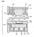
- a conventional resin encapsulation molding apparatus is provided with, for example as shown in Fig. 8, a mold consisting of an upper mold 31 and a lower mold 32. Further, the resin encapsulation molding apparatus is provided with a release film supplying mechanism (not shown) for providing a release film 34 between upper mold 31 and lower mold 32, applying a prescribed tension to release film 34.
- the resin encapsulation molding apparatus is further provided with a seal member 42 for making the inside of the mold to an outer air blocking space 41 before the mold is clamped. Further, the resin encapsulation molding apparatus is provided with a vacuum mechanism (not shown) for evacuating outer air blocking space 41.
- a substrate 36 is provided with resin encapsulation molding.
- Substrate 36 is provided with a semiconductor chip (an electronic part) 37 and a wire 38 that electrically connects substrate 36 and chip 37.
- a cavity 35 is provided to a mold surface 33 of lower mold 32. Cavity 35 is filled with a molten resin.
- chip 37 and wire 38 are commonly provided with resin encapsulation molding.
- a suction port 40 communicating with a mechanism for suctioning a release film (not shown) is provided to the bottom surface of cavity 35 of lower mold 32.
- release film 34 covers cavity 35 of lower 32 conforming to the contour thereof, with a prescribed tension.
- fixing means 39 are provided to mold surface 33 of upper mold 31 for fixing the position of substrate 36.
- substrate 36 can be fixed to upper mold 31, with semiconductor chip 37 and wire 38 facing downward.
- the conventional resin encapsulation molding method is as follows.
- upper mold 31 and lower mold 32 are mold-open (unclamped). Then, the main surface of substrate 36 to which semiconductor chip 37 and wire 38 are attached is faced downward. In this state, fixing means 39 are activated to attach substrate 36 to mold surface 33 of upper mold 31. Additionally, release film 34 with a prescribed tension covers along the surface of cavity 34 of lower mold 32. This is performed by evacuating air from the mold through release film suction port 40. Subsequently, before upper mold 31 and lower mold 32 are clamped, the function of seal member 42 is used to form outer air blocking space 41 by release film 34 covering along the surface of cavity 35 of lower mold 32 and upper mold 31.
- outer air blocking space 41 is evacuated through air vacuum hole 43 by the function of the vacuum mechanism. Then, in the state performing the evacuation of the mold, upper mold 31 and lower mold 32 are completely clamped. Next, cavity 35 covered by release film 34 is filled with a molten resin. Thus, the molten resin covers semiconductor chip 37 and wire 38 mounted on substrate 36. Thereafter, the molten resin cures. As a result, an encapsulated substrate, in which the cured resin is formed on substrate 36, is formed.
- Suction force A is for evacuating through suction hole 40.
- suction force A is for causing release film 34 to cover mold surface 33 of lower mold 32 and the contour of cavity 35.
- suction force B is for evacuating through air vacuum hole 43.
- suction force B is for forming outer air blocking space 41 between release film 34 and upper mold 31 using seal member 42 provided on mold surface 33 of upper mold 31.
- EP 1189270 relates to semiconductor devices having a chip-size package wherein an increased number of pins is employed to increase the integration density, the size of the semiconductor device is reduced, and external connection terminals are arranged at a reduced pitch.
- a resin layer is formed on the surface of the semiconductor element so as to seal the protruding electrodes except for the end portions thereof.
- US 6,471,501 discloses a molding apparatus used for molding a resin semiconductor package body.
- the object of the invention disclosed in US 6,471,501 is to hold the upper and lower molds in exact parallelism, such that a thin resin layer is formed on the surface of a semiconductor chip with a uniform thickness.
- the present invention is made considering the problems above, and an object of the present invention is to provide a resin encapsulation molding method in which deformation of an electronic part is prevented, and a resin encapsulation molding apparatus using the method.
- the resin encapsulation molding method is performed as follows.
- the resin encapsulation molding method of an electronic part comprises the steps of:
- the resin encapsulation molding can be performed in a state where the release film closely contacts the other main mold surface. Accordingly, the release film is prevented from moving into the enclosed space when the enclosed space is evacuated, in a state where the first, second and third molds are clamped. As a result, deformation of the electronic part is avoided.
- the step of clamping may include steps of clamping said second mold and said third mold and closely contacting said release film to said other main mold surface by sandwiching said release film using said second mold and said third mold to apply said prescribed tension to said release film; and thereafter, in this stage, clamping said third mold and said first mold.
- the release film since the release film does not move into the enclosed space when the first and third molds are clamped, it is ensured to avoid contact of the electronic part and the release film.
- a resin encapsulation molding apparatus has the structure used in the resin encapsulation molding method. Further, it is preferable that the resin encapsulation molding apparatus further includes a resilient mechanism for pressing the release film to the third mold when applying a prescribed tension to the release film. By this structure, the prescribed tension can easily be applied to the release film.
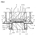
- a resin encapsulation molding apparatus includes, as shown in Figs. 1 and 2, a mold including an upper mold 1, a lower mold 2 arranged facing to upper mold 1, and an intermediate plate 3 provided between upper mold 1 and lower mold 2. Further, the resin encapsulation apparatus is provided with a release film supplying mechanism (not shown) for supplying a release film 4 for covering a mold surface 15b of lower mold 2 between lower mold 2 and intermediate plate 3.
- the mold is provided with a seal member 5 at the mold surface of upper mold 1 for forming an enclosed space 21 that separates cavity space 18 and outer air.
- Resin encapsulation forming apparatus is provided with a vacuum mechanism for forcibly evacuating enclosed space 21.
- the electronic part is provided with a semiconductor chip 7 die-bonded on a substrate 6 and a wire 8 electrically connecting substrate 6 and semiconductor chip 7.
- Upper mold 1 is provided with fixing means 9 for fixing substrate 6 to which the electronic part (semiconductor chip 7) and wire 8 are attached.
- Fixing means 9 fix substrate 6 to a mold surface 15a in a state in which semiconductor chip 7 and wire 8 are facing downward, as shown in Fig. 1.
- fixing means 9 are shown as arranged parallel to substrate 6. However, the arrangement of fixing means 9 is not limited to the arrangement shown in Fig. 1. Fixing means 9 may be, for example, a recess for setting (not shown) by which substrate 6 is set to mold surface 15a of upper mold 1.
- substrate 6 is fixed to mold surface 15a with semiconductor chip 7 and wire 8 facing downward. Then, semiconductor chip 7 and wire 8 are provided with resin encapsulation molding by a molten resin. Thereafter, the molten resin is cured to form a cured resin 10. As a result, the encapsulated substrate 11 is formed.
- intermediate plate 3 has mold surface 12 that forms a cavity arranged through intermediate plate 3 and to which semiconductor chip 7 attached to substrate 11 and wire 8 are fitted. Further, intermediate plate 3 has a slope surface 13 for clamping upper mold 1 and lower mold 2. Still further, intermediate plate 3 has a mold surface 24 for pressing release film 4. Intermediate plate 3 moves upward and downward by upward and downward movement of a support member 14 that supports intermediate plate 3.
- lower mold 2 is provided with mold surface 15b that is horizontal and joins to the bottom of mold surface 12 of intermediate plate 3.
- a member 16 that joins to mold surface 24 for sandwiching release film 4 is provided.
- Mold surface 15b and the upper surface of member 16 are provided approximately at the same plane.
- Member 16 for sandwiching release film 4 is provided with a resilient member 17 formed with a compression spring or the like. By the compression and expansion of resilient member 17 in the vertical direction, release film 4 is tensioned in the direction of its surface.
- Lower mold 2 is provided with a slope surface 23 that joins to slope surface 13 of intermediate plate 3 for tensioning release film 4.
- Slope surface 23 is arranged to face slope surface 13.
- release film 4 which is applied with a prescribed tension and held horizontally, is supplied to the mold by the release film supplying mechanism. Thereafter, when intermediate plate 3 and lower mold 2 are clamped, firstly support member 14 that supports intermediate plate 3 moves downward. Thus, release film 4 applied with a prescribed tension and mold surface 24 of intermediate plate 3 contact to each other. Thereafter, release film 4 is sandwiched by mold surface 24 and the upper surface of member 16.
- support member 14 further moves downward.
- resilient member 17 attached to member 16 is pressed and compresses.
- slope surface 13 of intermediate plate 3 and release film 4 contact to each other.
- the release film is pulled along the contour of slope surface 23 of the lower mold.
- slope surface 13 and slope surface 23 join, with release film 4 interposed between them.
- support member 14 of intermediate plate 3 further moves downward.
- the bottom side of mold surface 12 of intermediate plate 3 and mold surface 15b of lower mold 2 join, with release film 4 interposed between them.
- release film 4 covers mold surface 15b of lower mold 2, in a state being applied with a prescribed tension.
- cavity space 18 is formed by mold surface 12 of intermediate plate 3 and mold surface 15b of lower mold 2 covered with release film 4. Note that it is possible to forcibly evacuate cavity space 18 by a vacuum mechanism that is not shown.
- the condition of the release film when cavity space 18 (enclosed space 21) is forcibly evacuated is different from that of the conventional resin encapsulation molding method shown in Fig. 8.
- release film 4 is prevented from leaving from mold surface 15b of lower mold 2 by the presence of intermediate plate 3.
- a granulated resin 19 of a necessary amount is supplied from a resin material supplying mechanism (not shown) into cavity space 18.
- a resin material supplying mechanism not shown
- granulated resin 19 of the necessary amount supplied to cavity space 18 is heated and a molten resin 20 is formed.
- Granulated resin 19 turns to molten resin 20 before upper mold 1 and intermediate plate 3 are clamped.
- any means may be employed as long as it can heat cavity space 18, such as a heater embedded in the mold or a resin material heating and melting mechanism.
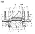
- Fig. 4 shows an intermediate (or an initial) clamping state of intermediate plate 3 and lower mold 2, and shows a state before upper mold 1 and intermediate plate 2 are fully clamped.
- seal member 5 provided to the mold surface of upper mold 1 contacts to the mold surface of intermediate plate 3 to form enclosed space 21. Further, when forcibly evacuating enclosed space 21 using a vacuum mechanism, the air is suctioned from air vacuum hole 22.
- release film 4 is tightly pinched by intermediate plate 3 and both of lower mold 2 and member 16. Therefore, when enclosed space 21 became a vacuum state due to the suction function of the vacuum mechanism, release film 4 is not detached (separated) from upper surface 15 b of lower mold 2.
- Seal member 5 provided to upper mold 1 is to render cavity space 18 to enclosed space 21, seal member 5 may not be provided and enclosed space 21 may be formed using the mold. Additionally, seal member 5 is capable of forming enclosed space 21 even when it is provided on the upper mold surface of intermediate plate 3.
- semiconductor chip 7 and wire 8 are gradually brought near to molten resin 20 in cavity space 18.
- electronic part (semiconductor chip 7) and wire 8 are gradually buried in resin 20.
- the periphery of substrate 6 is not provided with encapsulation molding.
- the periphery of substrate 6 abuts to the upper surface of intermediate plate 3 as shown in Figure 5.
- molten resin 20 does not leak. Thereafter, molten resin 20 that includes the electronic part (semiconductor chip 7) and wire 8 cures. In other words, molten resin 20 changes to cured resin 10. As a result, encapsulated substrate 11 is molded.
- Release film 4 after use is transported from immediately above mold surface 15b of lower mold 2 by the release film supplying mechanism.
- release film 4 before use is supplied from film supplying mechanism to the above of mold surface 15b of lower mold 2.
- encapsulated substrate 11 is released from the fixing of fixing means 9 after upper mold 1, lower mold 2 and intermediate plate 3 are mold-open. Thereafter, encapsulated substrate 11 is transported to other apparatus.
- substrate 6 before provided with encapsulation to which an electronic part (semiconductor chip 7) and wire 8 are attached is supplied to fixing means 9 of upper mold 1 and attached to a prescribed position. It should be noted that an interval may be provided between the step of clamping lower mold 2 and intermediate plate 3 and the step of clamping intermediate plate 3 and upper mold 1.
- the resin encapsulation molding method has been described using the mold consisting of movable upper mold 1, intermediate plate 3 moving reciprocally upward and downward, and lower mold 2 of which position is fixed.
- the resin encapsulation molding method can be carried out using a mold where the position of upper mold 1 is fixed and intermediate plate 3 and lower mold 2 are movable.
- the mold has been described by which the resin encapsulation molding step is carried out by closely contacting release film 4 to mold surface 15b of lower mold 2 using intermediate plate 3 and lower mold 2.
- another mold of different structure may be employed as long as it can carry out the resin encapsulation molding keeping release film 4 and mold surface 15b of lower mold 2 closely contacting to each other.
- granulated resin 19 has been employed in the present embodiment, a liquid resin or a powder resin may be employed. Still further, in the present embodiment, the example has been described where an electronic part that is wire-bonded is provided with resin encapsulation molding. However, with a flip-chip substrate to which an electronic part without wire 8 is provided, the resin encapsulation molding method can be carried out. In this case, a tablet-type resin may be employed for the resin encapsulation.
- the resin encapsulation molding apparatus may have an ejector mechanism (not shown) that is capable of pushing out encapsulated substrate 11 with release film 4 interposed between them when encapsulated substrate 11 and release film 4 are separated.
- This ejector mechanism is preferably embedded into lower mold 2 so that it can accept redundant molten resin 20 when it is excessively supplied.
- semiconductor chip 7 as an electronic part and wire 8 are set to the resin encapsulation mold in the state facing downward.
- the upper and lower molds of the resin encapsulation mold may be arranged reversely as compared to the present embodiment.
- semiconductor chip 7 and wire 8 are set to the lower mold in a state facing upward.
- An attachment holder 101 is removably provided to the body of upper mold 100 of the resin encapsulation molding apparatus.
- Attachment holder 101 is provided with an upper mold block 102, a film holding member 103 provided to surround upper mold block 102, and a resilient member 104 that enables the slidable reciprocal movement of film holding member 103 in upward and downward direction.
- Upper mold block 102, film holding member 103 and resilient member 104 are removably provided to attachment holder 101.
- a seal member 500 is provided to the body so as to be joined to an intermediate mold 300 when clamping of upper mold 100 and lower mold 300 are completed.
- Intermediate mold 300 is provided with a cavity (a through hole) 180 that is provided to pass through intermediate mold 300 in a width direction and accommodating an electronic part (a semiconductor chip 700 and a wire 800) 110 attached to an upper surface of substrate 600 before provided with resin encapsulation.
- Cavity 180 has side surfaces 120, 130.
- each of release film 400 applied with tension by a lower surface 200b of upper mold 100 and seal member 500 of upper mold 100 contact to the upper surface of intermediate mold 300.
- a resin path 301 for injecting a resin material that is heated and molten into cavity 180 is provided to the upper surface of intermediate mold 300.
- Attachment holder 201 is removably provided to the body of lower mold 200.
- Attachment holder 201 is provided with a sliding member 202 for resiliently supporting substrate 6 before provided with resin encapsulation to which the electronic part (semiconductor chip700 and wire 800) are attached in a state facing upward, and a resilient member 203 for enabling reciprocal movement of sliding member 202 in upward and downward direction.
- Sliding member 202 and resilient member 203 are removably attached to attachment holder 201.
- seal member 500 is joined to intermediate mold 300 when lower mold 200 and intermediate mold 300 are clamped.
- Such a resin encapsulation molding apparatus shown in Figs. 6 and 7 has substantially the same structure to the previous embodiment except for the following points:
Landscapes
- Engineering & Computer Science (AREA)
- Mechanical Engineering (AREA)
- Computer Hardware Design (AREA)
- Power Engineering (AREA)
- Microelectronics & Electronic Packaging (AREA)
- Manufacturing & Machinery (AREA)
- Condensed Matter Physics & Semiconductors (AREA)
- General Physics & Mathematics (AREA)
- Physics & Mathematics (AREA)
- Encapsulation Of And Coatings For Semiconductor Or Solid State Devices (AREA)
- Injection Moulding Of Plastics Or The Like (AREA)
- Moulds For Moulding Plastics Or The Like (AREA)
- Casting Or Compression Moulding Of Plastics Or The Like (AREA)
Claims (5)
- Kunstharz-Einschließverfahren für ein elektronisches Bauteil, das folgende Schritte umfasst:- Einrichten einer ersten Gießform (200) mit einer ersten Form-Hauptfläche (200a);- Einrichten einer zweiten Gießform (100) mit einer zweiten Form-Hauptfläche (200b), die der ersten Hauptfläche (200a) gegenüber liegt;- Einrichten einer dritten Gießform (300), die eine Form-Seitenfläche (120) zwischen der ersten Form-Hauptfläche (200a) und der zweiten Form-Hauptfläche (200b) bildet;- Einsetzen eines elektronischen Bauteils (110) in die erste Gießform (200);- eine Trennfolie (400) mit der zweiten Form-Hauptfläche (200b) in direkten Kontakt bringen, indem die Trennfolie (400) zwischen der zweiten Gießform (100) und der dritten Gießform (300) eingebunden wird, um die Trennfolie (400) unter eine vorbestimmte Spannung zu setzen;- Zusammenschließen der ersten Gießform (200) mit der zweiten Gießform (100) und der dritten Gießform (300), um einen das elektronische Bauteil (110) enthaltenden abgeschlossenen Raum (210) zu bilden, nämlich mittels der ersten Form-Hauptfläche (200a), der zweiten Form-Hauptfläche (200b) und der Form-Seitenfläche (120);- Füllen des abgeschlossenen Raums (210) mit einem geschmolzenen Kunstharz (220); und- Einschließen des elektronischen Bauteils (110) in Kunstharz durch Aushärten des geschmolzenen Kunstharzes (220).
- Kunstharz-Einschließverfahren nach Anspruch 1, bei dem der Schritt des Zusammenschließens folgende Schritte umfasst: Zusammenschließen der zweiten Gießform (100) und der dritten Gießform (300) und Herstellen eines direkten Kontakts der Trennfolie (400) mit der zweiten Form-Hauptfläche (200b) durch Einbinden der Trennfolie (400) mittels der zweiten Gießform (100) und der dritten Gießform (300), um die Trennfolie (400) wie vorgeschrieben zu spannen; und anschließend, in diesem Stadium, Zusammenschließen der dritten Gießform (300) und der ersten Gießform (100).
- Kunstharz-Einschließverfahren nach Anspruch 1, bei dem der Schritt, die Trennfolie (400) in direkten Kontakt mit der zweiten Form-Hauptfläche (200b) zu bringen, indem die Trennfolie (400) wie vorgeschrieben gespannt wird, ausgeführt wird, indem die Trennfolie (400) auf die dritte Gießform (300) durch die elastische Kraft eines Federmechanismus (103, 104) gepresst wird.
- Kunstharz-Einschließverfahren nach Anspruch 1, bei dem der Schritt zur Herstellung des Einschlusses in Kunstharz in einem Stadium durchgerührt wird, wo der abgeschlossene Raum (210) unter Vakuum steht.
- Vorrichtung für das Kunstharz-Einschließverfahren, die Mittel umfasst für die Durchführung jedes der genannten Schritte des Verfahrens zum Einschließen eines elektronischen Bauteils in Kunstharz entsprechend Anspruch 1.
Priority Applications (1)
| Application Number | Priority Date | Filing Date | Title |
|---|---|---|---|
| EP07006851A EP1803539B1 (de) | 2002-09-06 | 2003-08-18 | Kunststoffformverfahren zur Verkapselung von elektronischem Bauteil und dafür verwendete Verkapselungs-Kunststoffformeinrichtung |
Applications Claiming Priority (2)
| Application Number | Priority Date | Filing Date | Title |
|---|---|---|---|
| JP2002260894 | 2002-09-06 | ||
| JP2002260894A JP4268389B2 (ja) | 2002-09-06 | 2002-09-06 | 電子部品の樹脂封止成形方法及び装置 |
Related Child Applications (1)
| Application Number | Title | Priority Date | Filing Date |
|---|---|---|---|
| EP07006851A Division EP1803539B1 (de) | 2002-09-06 | 2003-08-18 | Kunststoffformverfahren zur Verkapselung von elektronischem Bauteil und dafür verwendete Verkapselungs-Kunststoffformeinrichtung |
Publications (2)
| Publication Number | Publication Date |
|---|---|
| EP1396323A1 EP1396323A1 (de) | 2004-03-10 |
| EP1396323B1 true EP1396323B1 (de) | 2007-12-05 |
Family
ID=31712334
Family Applications (2)
| Application Number | Title | Priority Date | Filing Date |
|---|---|---|---|
| EP07006851A Expired - Fee Related EP1803539B1 (de) | 2002-09-06 | 2003-08-18 | Kunststoffformverfahren zur Verkapselung von elektronischem Bauteil und dafür verwendete Verkapselungs-Kunststoffformeinrichtung |
| EP03018539A Expired - Fee Related EP1396323B1 (de) | 2002-09-06 | 2003-08-18 | Kunststoffformverfahren zum Einschliessen eines elektronischen Bauteils in Harz und dazu verwendbare Vorrichtung |
Family Applications Before (1)
| Application Number | Title | Priority Date | Filing Date |
|---|---|---|---|
| EP07006851A Expired - Fee Related EP1803539B1 (de) | 2002-09-06 | 2003-08-18 | Kunststoffformverfahren zur Verkapselung von elektronischem Bauteil und dafür verwendete Verkapselungs-Kunststoffformeinrichtung |
Country Status (6)
| Country | Link |
|---|---|
| US (1) | US6977188B2 (de) |
| EP (2) | EP1803539B1 (de) |
| JP (1) | JP4268389B2 (de) |
| KR (1) | KR100546191B1 (de) |
| DE (2) | DE60317864D1 (de) |
| TW (1) | TWI235703B (de) |
Families Citing this family (52)
| Publication number | Priority date | Publication date | Assignee | Title |
|---|---|---|---|---|
| JP4094515B2 (ja) * | 2003-09-26 | 2008-06-04 | 株式会社ルネサステクノロジ | 半導体装置の製造方法 |
| JP2005150350A (ja) * | 2003-11-14 | 2005-06-09 | Renesas Technology Corp | 半導体装置の製造方法 |
| JP4373237B2 (ja) * | 2004-02-13 | 2009-11-25 | Towa株式会社 | 半導体チップの樹脂封止成形方法および樹脂封止成形用金型 |
| JP5004410B2 (ja) | 2004-04-26 | 2012-08-22 | Towa株式会社 | 光素子の樹脂封止成形方法および樹脂封止成形装置 |
| JP5128047B2 (ja) | 2004-10-07 | 2013-01-23 | Towa株式会社 | 光デバイス及び光デバイスの生産方法 |
| JP4508839B2 (ja) * | 2004-11-12 | 2010-07-21 | パナソニック株式会社 | 樹脂封止金型および樹脂封止装置 |
| US7344902B2 (en) * | 2004-11-15 | 2008-03-18 | Philips Lumileds Lighting Company, Llc | Overmolded lens over LED die |
| US7452737B2 (en) * | 2004-11-15 | 2008-11-18 | Philips Lumileds Lighting Company, Llc | Molded lens over LED die |
| US7858408B2 (en) * | 2004-11-15 | 2010-12-28 | Koninklijke Philips Electronics N.V. | LED with phosphor tile and overmolded phosphor in lens |
| WO2006129343A1 (ja) | 2005-05-30 | 2006-12-07 | Spansion Llc | 半導体装置の製造装置及び半導体装置の製造方法 |
| JP4587881B2 (ja) * | 2005-06-10 | 2010-11-24 | サンユレック株式会社 | 樹脂封止装置 |
| US7985357B2 (en) * | 2005-07-12 | 2011-07-26 | Towa Corporation | Method of resin-sealing and molding an optical device |
| JP2007109831A (ja) * | 2005-10-13 | 2007-04-26 | Towa Corp | 電子部品の樹脂封止成形方法 |
| US7595515B2 (en) * | 2005-10-24 | 2009-09-29 | 3M Innovative Properties Company | Method of making light emitting device having a molded encapsulant |
| CN101297411B (zh) * | 2005-10-24 | 2010-05-19 | 3M创新有限公司 | 发光器件的制造方法及发光器件 |
| JP4741383B2 (ja) * | 2006-02-17 | 2011-08-03 | 富士通セミコンダクター株式会社 | 電子部品の樹脂封止方法 |
| US8092735B2 (en) | 2006-08-17 | 2012-01-10 | 3M Innovative Properties Company | Method of making a light emitting device having a molded encapsulant |
| JP4858966B2 (ja) * | 2006-11-02 | 2012-01-18 | Towa株式会社 | 電子部品の圧縮成形方法及び成形装置 |
| EP2111651A4 (de) * | 2007-02-13 | 2011-08-17 | 3M Innovative Properties Co | Led mit linsen und verfahren zu ihrer herstellung |
| JP5036372B2 (ja) * | 2007-04-02 | 2012-09-26 | Towa株式会社 | 光電子部品および光電子部品の製造方法 |
| US7915089B2 (en) * | 2007-04-10 | 2011-03-29 | Infineon Technologies Ag | Encapsulation method |
| KR101132136B1 (ko) * | 2007-08-03 | 2012-04-03 | 스미도모쥬기가이고교 가부시키가이샤 | 피성형품의 낙하 방지 기구 |
| JP2009124012A (ja) * | 2007-11-16 | 2009-06-04 | Towa Corp | 電子部品の圧縮成形方法及び金型 |
| JP4553944B2 (ja) * | 2008-01-10 | 2010-09-29 | アピックヤマダ株式会社 | 樹脂モールド方法および樹脂モールド装置 |
| KR100980299B1 (ko) | 2008-02-27 | 2010-09-06 | 세크론 주식회사 | 전자 부품 몰딩 장치 |
| US7875967B2 (en) * | 2008-03-10 | 2011-01-25 | Stats Chippac Ltd. | Integrated circuit with step molded inner stacking module package in package system |
| JP5153509B2 (ja) * | 2008-08-08 | 2013-02-27 | Towa株式会社 | 電子部品の圧縮成形方法及び金型装置 |
| US20100120199A1 (en) * | 2008-11-07 | 2010-05-13 | Bok Sim Lim | Stacked package-on-package semiconductor device and methods of fabricating thereof |
| WO2010146860A1 (ja) * | 2009-06-17 | 2010-12-23 | パナソニック株式会社 | 樹脂モールド型電子部品の製造方法 |
| KR101101669B1 (ko) | 2009-12-01 | 2011-12-30 | 삼성전기주식회사 | 전자부품 제조장치 및 전자부품 제조방법 |
| US8771577B2 (en) * | 2010-02-16 | 2014-07-08 | Koninklijke Philips N.V. | Light emitting device with molded wavelength converting layer |
| WO2011105640A1 (ko) * | 2010-02-25 | 2011-09-01 | 한미반도체 주식회사 | 압축 성형장치 및 압축 성형방법 |
| WO2011105639A1 (ko) * | 2010-02-25 | 2011-09-01 | 한미반도체 주식회사 | 압축 성형 장치 및 방법 |
| JP5576197B2 (ja) * | 2010-07-08 | 2014-08-20 | Towa株式会社 | 電子部品の圧縮成形方法及び成形装置 |
| KR101052324B1 (ko) | 2011-03-23 | 2011-07-27 | 신한다이아몬드공업 주식회사 | 봉지재 성형 방법 |
| JP5403012B2 (ja) * | 2011-08-11 | 2014-01-29 | 第一精工株式会社 | 樹脂封止装置 |
| DE102011081083A1 (de) * | 2011-08-17 | 2013-02-21 | Osram Ag | Presswerkzeug und verfahren zum pressen eines silikonelements |
| US9159643B2 (en) | 2012-09-14 | 2015-10-13 | Freescale Semiconductor, Inc. | Matrix lid heatspreader for flip chip package |
| US8921994B2 (en) | 2012-09-14 | 2014-12-30 | Freescale Semiconductor, Inc. | Thermally enhanced package with lid heat spreader |
| JP5786918B2 (ja) * | 2013-10-23 | 2015-09-30 | 第一精工株式会社 | 樹脂封止金型およびこれを用いた樹脂封止装置、樹脂封止方法 |
| JP6057880B2 (ja) * | 2013-11-28 | 2017-01-11 | Towa株式会社 | 圧縮成形装置の樹脂材料供給方法及び供給装置 |
| JP6143665B2 (ja) * | 2013-12-26 | 2017-06-07 | Towa株式会社 | 半導体封止方法及び半導体封止装置 |
| KR102335853B1 (ko) * | 2014-01-14 | 2021-12-07 | 아피쿠 야마다 가부시키가이샤 | 수지 몰드 금형 및 수지 몰드 방법 |
| JP6270571B2 (ja) * | 2014-03-19 | 2018-01-31 | Towa株式会社 | シート樹脂の供給方法と半導体封止方法及び半導体封止装置 |
| NL2013978B1 (en) * | 2014-12-15 | 2016-10-11 | Besi Netherlands Bv | Device and method for controlled moulding and degating of a carrier with electronic components and moulded product. |
| JP6304517B1 (ja) * | 2017-02-14 | 2018-04-04 | 第一精工株式会社 | 樹脂封止方法及び樹脂封止装置 |
| CN108448012A (zh) * | 2018-03-01 | 2018-08-24 | 佛山市国星光电股份有限公司 | 全彩led显示模组及其封装方法和显示屏 |
| JP6994445B2 (ja) * | 2018-08-31 | 2022-01-14 | Towa株式会社 | 樹脂成形装置、離型フィルムの剥離方法、樹脂成形品の製造方法 |
| JP7018377B2 (ja) * | 2018-11-26 | 2022-02-10 | Towa株式会社 | 成形型、樹脂成形装置、樹脂成形品の製造方法 |
| JP7134926B2 (ja) * | 2019-07-10 | 2022-09-12 | Towa株式会社 | 樹脂成形装置、及び樹脂成形品の製造方法 |
| CN112873810A (zh) * | 2019-11-29 | 2021-06-01 | 复盛应用科技股份有限公司 | 高尔夫球杆头盖片制造方法及模具 |
| TWI740322B (zh) * | 2019-12-25 | 2021-09-21 | 明安國際企業股份有限公司 | 具有碳纖維板之高爾夫球桿頭及其製造方法 |
Family Cites Families (3)
| Publication number | Priority date | Publication date | Assignee | Title |
|---|---|---|---|---|
| CN1110846C (zh) | 1996-07-12 | 2003-06-04 | 富士通株式会社 | 半导体装置的制造方法 |
| JP3282988B2 (ja) * | 1997-05-01 | 2002-05-20 | アピックヤマダ株式会社 | 樹脂モールド方法及び樹脂モールド装置 |
| JP3490606B2 (ja) | 1998-03-20 | 2004-01-26 | 富士通株式会社 | 半導体装置製造用金型 |
-
2002
- 2002-09-06 JP JP2002260894A patent/JP4268389B2/ja not_active Expired - Fee Related
-
2003
- 2003-08-15 TW TW092122493A patent/TWI235703B/zh not_active IP Right Cessation
- 2003-08-15 US US10/641,606 patent/US6977188B2/en not_active Expired - Fee Related
- 2003-08-18 EP EP07006851A patent/EP1803539B1/de not_active Expired - Fee Related
- 2003-08-18 DE DE60317864T patent/DE60317864D1/de not_active Expired - Lifetime
- 2003-08-18 DE DE60321977T patent/DE60321977D1/de not_active Expired - Fee Related
- 2003-08-18 EP EP03018539A patent/EP1396323B1/de not_active Expired - Fee Related
- 2003-08-22 KR KR1020030058173A patent/KR100546191B1/ko active IP Right Grant
Also Published As
| Publication number | Publication date |
|---|---|
| TWI235703B (en) | 2005-07-11 |
| EP1803539B1 (de) | 2008-07-02 |
| JP4268389B2 (ja) | 2009-05-27 |
| TW200406293A (en) | 2004-05-01 |
| KR100546191B1 (ko) | 2006-01-24 |
| JP2004098364A (ja) | 2004-04-02 |
| EP1396323A1 (de) | 2004-03-10 |
| US20040048416A1 (en) | 2004-03-11 |
| DE60317864D1 (de) | 2008-01-17 |
| DE60321977D1 (de) | 2008-08-14 |
| EP1803539A1 (de) | 2007-07-04 |
| KR20040022152A (ko) | 2004-03-11 |
| US6977188B2 (en) | 2005-12-20 |
Similar Documents
| Publication | Publication Date | Title |
|---|---|---|
| EP1396323B1 (de) | Kunststoffformverfahren zum Einschliessen eines elektronischen Bauteils in Harz und dazu verwendbare Vorrichtung | |
| US7618573B2 (en) | Resin sealing method for electronic part and mold used for the method | |
| JP4077118B2 (ja) | 半導体装置の製造方法および半導体装置製造用金型 | |
| US20080187613A1 (en) | Method of manufacturing wafer-level chip-size package and molding apparatus used in the method | |
| US6444500B1 (en) | Split-mold and method for manufacturing semiconductor device by using the same | |
| WO2007132611A1 (ja) | 電子部品の樹脂封止成形方法 | |
| US6630374B2 (en) | Resin sealing method and resin sealing apparatus | |
| JP2005219297A (ja) | 樹脂モールド方法および樹脂モールド装置 | |
| JP2002036270A (ja) | 樹脂封止方法及び樹脂封止装置 | |
| JP4052939B2 (ja) | 電子部品の樹脂封止成形方法及び装置 | |
| JP6175592B1 (ja) | 樹脂封止装置及び樹脂封止方法 | |
| JP4011781B2 (ja) | 半導体ウェーハの樹脂被覆方法 | |
| JP2004230707A (ja) | 電子部品の樹脂封止成形方法及び装置 | |
| JPWO2018147305A1 (ja) | 樹脂封止装置及び樹脂封止方法 | |
| JP4253393B2 (ja) | 半導体ウェーハの樹脂被覆方法及び金型 | |
| JP4358501B2 (ja) | 電子部品の樹脂封止成形方法及び金型 | |
| JP2005324341A (ja) | 樹脂モールド方法および樹脂モールド装置 | |
| TW201637812A (zh) | 樹脂成形模具、樹脂成形方法、及成形品的製造方法 | |
| US6093583A (en) | Semiconductor component and method of manufacture | |
| JP3139981B2 (ja) | チップサイズパッケージの樹脂封止方法及び樹脂封止装置 | |
| JP2005225067A (ja) | 樹脂モールド方法および樹脂モールド装置 | |
| CN113573867B (zh) | 树脂成形装置以及树脂成形品的制造方法 | |
| JP5027451B2 (ja) | 半導体チップの樹脂封止成形方法 | |
| JP2001168121A (ja) | 電子部品の樹脂封止成形方法 | |
| JP2005236133A (ja) | 樹脂封止成形方法 |
Legal Events
| Date | Code | Title | Description |
|---|---|---|---|
| PUAI | Public reference made under article 153(3) epc to a published international application that has entered the european phase |
Free format text: ORIGINAL CODE: 0009012 |
|
| AK | Designated contracting states |
Kind code of ref document: A1 Designated state(s): AT BE BG CH CY CZ DE DK EE ES FI FR GB GR HU IE IT LI LU MC NL PT RO SE SI SK TR |
|
| AX | Request for extension of the european patent |
Extension state: AL LT LV MK |
|
| 17P | Request for examination filed |
Effective date: 20040112 |
|
| 17Q | First examination report despatched |
Effective date: 20040419 |
|
| AKX | Designation fees paid |
Designated state(s): DE NL |
|
| 17Q | First examination report despatched |
Effective date: 20040419 |
|
| GRAP | Despatch of communication of intention to grant a patent |
Free format text: ORIGINAL CODE: EPIDOSNIGR1 |
|
| GRAS | Grant fee paid |
Free format text: ORIGINAL CODE: EPIDOSNIGR3 |
|
| RIN1 | Information on inventor provided before grant (corrected) |
Inventor name: TAKASE, SHINJIC/O TOWA CORPORATION |
|
| GRAA | (expected) grant |
Free format text: ORIGINAL CODE: 0009210 |
|
| AK | Designated contracting states |
Kind code of ref document: B1 Designated state(s): DE NL |
|
| REF | Corresponds to: |
Ref document number: 60317864 Country of ref document: DE Date of ref document: 20080117 Kind code of ref document: P |
|
| PLBE | No opposition filed within time limit |
Free format text: ORIGINAL CODE: 0009261 |
|
| STAA | Information on the status of an ep patent application or granted ep patent |
Free format text: STATUS: NO OPPOSITION FILED WITHIN TIME LIMIT |
|
| PG25 | Lapsed in a contracting state [announced via postgrant information from national office to epo] |
Ref country code: DE Free format text: LAPSE BECAUSE OF FAILURE TO SUBMIT A TRANSLATION OF THE DESCRIPTION OR TO PAY THE FEE WITHIN THE PRESCRIBED TIME-LIMIT Effective date: 20080306 |
|
| 26N | No opposition filed |
Effective date: 20080908 |
|
| PGFP | Annual fee paid to national office [announced via postgrant information from national office to epo] |
Ref country code: NL Payment date: 20090814 Year of fee payment: 7 |
|
| REG | Reference to a national code |
Ref country code: NL Ref legal event code: V1 Effective date: 20110301 |
|
| PG25 | Lapsed in a contracting state [announced via postgrant information from national office to epo] |
Ref country code: NL Free format text: LAPSE BECAUSE OF NON-PAYMENT OF DUE FEES Effective date: 20110301 |