EP1369935A1 - LED contenant des nanoparticules - Google Patents
LED contenant des nanoparticules Download PDFInfo
- Publication number
- EP1369935A1 EP1369935A1 EP20030076772 EP03076772A EP1369935A1 EP 1369935 A1 EP1369935 A1 EP 1369935A1 EP 20030076772 EP20030076772 EP 20030076772 EP 03076772 A EP03076772 A EP 03076772A EP 1369935 A1 EP1369935 A1 EP 1369935A1
- Authority
- EP
- European Patent Office
- Prior art keywords
- light
- particles
- emitting device
- wavelength
- emitting
- Prior art date
- Legal status (The legal status is an assumption and is not a legal conclusion. Google has not performed a legal analysis and makes no representation as to the accuracy of the status listed.)
- Granted
Links
Images


Classifications
-
- H—ELECTRICITY
- H01—ELECTRIC ELEMENTS
- H01L—SEMICONDUCTOR DEVICES NOT COVERED BY CLASS H10
- H01L33/00—Semiconductor devices with at least one potential-jump barrier or surface barrier specially adapted for light emission; Processes or apparatus specially adapted for the manufacture or treatment thereof or of parts thereof; Details thereof
- H01L33/48—Semiconductor devices with at least one potential-jump barrier or surface barrier specially adapted for light emission; Processes or apparatus specially adapted for the manufacture or treatment thereof or of parts thereof; Details thereof characterised by the semiconductor body packages
- H01L33/50—Wavelength conversion elements
- H01L33/501—Wavelength conversion elements characterised by the materials, e.g. binder
-
- H—ELECTRICITY
- H01—ELECTRIC ELEMENTS
- H01L—SEMICONDUCTOR DEVICES NOT COVERED BY CLASS H10
- H01L33/00—Semiconductor devices with at least one potential-jump barrier or surface barrier specially adapted for light emission; Processes or apparatus specially adapted for the manufacture or treatment thereof or of parts thereof; Details thereof
- H01L33/48—Semiconductor devices with at least one potential-jump barrier or surface barrier specially adapted for light emission; Processes or apparatus specially adapted for the manufacture or treatment thereof or of parts thereof; Details thereof characterised by the semiconductor body packages
- H01L33/52—Encapsulations
- H01L33/56—Materials, e.g. epoxy or silicone resin
-
- H—ELECTRICITY
- H01—ELECTRIC ELEMENTS
- H01L—SEMICONDUCTOR DEVICES NOT COVERED BY CLASS H10
- H01L2933/00—Details relating to devices covered by the group H01L33/00 but not provided for in its subgroups
- H01L2933/0091—Scattering means in or on the semiconductor body or semiconductor body package
Definitions
- the present invention relates to light-emitting devices, and more particularly to semiconductor light-emitting devices.
- LEDs light-emitting diodes
- LDs laser diodes
- III-V semiconductors particularly binary, ternary, and quaternary alloys of gallium, aluminum, indium, and nitrogen, also referred to as III-nitride materials
- III-phosphide materials binary, ternary, and quaternary alloys of gallium, aluminum, indium, and phosphorus
- a common problem with conventional semiconductor light-emitting devices is that the efficiency with which light may be extracted from such a device is reduced by total internal reflection at interfaces between the device and the surrounding environment followed by reabsorption of the reflected light in the device.
- Such total internal reflection occurs because the index of refraction of the semiconductor materials from which the device is formed at the emission wavelengths of the device (n ⁇ 3.5 for III-Phosphide materials, for example) is larger than the index of refraction of the material, typically an epoxy or silicone (n ⁇ 1.5 or less), in which the device is packaged or encapsulated. Losses due to total internal reflection increase rapidly with the ratio of the refractive index inside the device to that outside the device.
- Another aspect of conventional semiconductor light-emitting devices which may be disadvantageous for some applications is that the emission spectrum of such a device typically exhibits a single rather narrow peak (full width at half maximum of about 15 to about 50 nanometers, for example) at a wavelength (peak wavelength) determined by the structure of the light-emitting semiconductor device and by the composition of the materials from which it is constructed.
- Some applications require a broader emission spectrum than can be directly produced by a conventional light-emitting semiconductor device. For example, some lighting applications require the production of apparently white light.
- the efficiency with which a conventional light-emitting semiconductor device generates light typically varies as the structure and composition of the device is changed to tune the narrow emission spectrum. Consequently, conventional light-emitting semiconductor devices may be unsatisfactory for applications requiring efficient generation of light at particular wavelengths.
- phosphor refers to any luminescent material which absorbs light of one wavelength and emits light of a different wavelength. For example, blue light from a light-emitting semiconductor device may be used to excite a yellow emitting phosphor. The resulting yellow light may be mixed with unabsorbed blue light to produce white light.
- Light-emitting devices in which emission from a semiconductor light-emitting device is converted by a phosphor to another wavelength are typically termed "phosphor converted light-emitting devices.” Unfortunately, such phosphor converted light-emitting devices are typically not as efficient as is desired.
- What is needed is a semiconductor light-emitting device having improved light extraction, improved phosphor conversion, or both.
- a light-emitting device comprises a light source emitting first light, a first material substantially transparent to and located to receive at least a portion of the first light, and particles of a second material dispersed in the first material.
- the second material has an index of refraction greater than an index of refraction of the first material at a wavelength of the first light.
- the particles have diameters less than about this wavelength, and do not substantially absorb light of this wavelength.
- the light source may be, for example, a light-emitting semiconductor device.
- the light-emitting devices of these embodiments may further comprise particles of a third material dispersed in the first material.
- the particles of the third material absorb at least a portion of the first light and emit second light having a greater wavelength.
- the first material and the particles of the second material may together provide a medium having a refractive index that approximately matches that of the third material at a wavelength of the first light.
- a light-emitting device comprises a light source emitting first light, a first material substantially transparent to and located to receive at least a portion of the first light, particles of a second material dispersed in the first material, and particles of a third material dispersed in the first material.
- the second material has an index of refraction greater than an index of refraction of the first material at a wavelength of the first light.
- the particles of the second material have diameters less than about this wavelength.
- the particles of the third material have diameters greater than about this wavelength.
- the light source may be, for example, a light-emitting semiconductor device.
- the particles of the second material absorb at least a portion of the first light and emit second light having a greater wavelength.
- the particles of the third material may also absorb at least a portion of the first light and emit light having a greater wavelength.
- the first material and the particles of the second material may together provide a medium having a refractive index that approaches or approximately matches that of the third material at a wavelength of the first light.
- Light-emitting devices in accordance with some embodiments may be fabricated by a method comprising providing a light source that emits first light, providing a first material in optical communication with the light source, and dispersing particles of a second material in the first material.
- the first material is substantially transparent to the first light.
- the second material has an index of refraction greater than an index of refraction of the first material at a wavelength of the first light.
- the particles of the second material have diameters less than about this wavelength.
- the dispersing is such that the first material together with the particles of the second material provide a medium having a particular refractive index.
- the light-emitting devices disclosed herein may advantageously exhibit increased light extraction from a primary light source, increased light extraction from phosphor particles, and decreased light scattering by phosphor particles compared to conventional light-emitting devices.
- nanoparticle refers to a particle having a diameter (or similar cross-sectional dimension) typically much less than about one micron.
- Such nanoparticles may be of any shape and may comprise, for example, crystalline or amorphous solids or liquids.
- the inventors have discovered that the efficiency of conventional phosphor converted light-emitting devices is significantly decreased by scattering by the phosphor particles of both the primary emission from the semiconductor device and the secondary emission from the phosphor particles. A portion of the light scattered by the phosphor particles is scattered onto absorbing parts of the semiconductor device or its package and thereby lost.
- Such scattering by the phosphor particles occurs because they are typically substantially larger than the wavelengths of the primary and secondary emitted light, and because the phosphor particles typically have refractive indices at these wavelengths that are much larger than the surrounding medium.
- conventional phosphor converted light-emitting devices typically utilize phosphor particles having diameters of about 2 microns ( ⁇ m) to about 20 ⁇ m.
- visible light is conventionally defined to include wavelengths from about 380 nanometers (nm) to about 770 run.
- Such conventional phosphor particles which typically have indices of refraction of about 1.7 to about 2.3 for visible light, are typically embedded in an epoxy or silicone host material having an index of refraction of about 1.5 at these wavelengths.
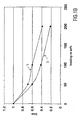
- Fig. 1A The effect of such scattering on the efficiency of phosphor converted light-emitting semiconductor devices is shown, for example, in the plot in Fig. 1A.
- blue emission from a III-Nitride light-emitting diode (LED) is converted to green light by europium-doped strontium thiogallate phosphor particles (having diameters of about 4 ⁇ m to about 5 ⁇ m) dispersed in a silicone resin disposed on the LED.
- the horizontal axis of the plot labeled "blue fraction,” represents the percentage of the blue light emitted by the LED that is unabsorbed and unconverted and hence present in the total light output of the phosphor-converted device.
- the horizontal axis also represents the phosphor loading in the resin, with the phosphor loading decreasing along the axis from left to right.
- the left vertical axis of the plot represents the total light output, in lumens (1m), of the phosphor converted device.
- the right vertical axis labeled “package gain,” represents a scaling factor by which a theoretical prediction of the total light output, based on the known characteristics of the LED and of the phosphor and neglecting scattering, must be multiplied to match the measured performance of the phosphor converted devices.
- An ideal device would have a "package gain" of one.
- the right vertical axis measures the degree to which scattering by the phosphor particles has degraded the performance of the device.
- lower values of "package gain” indicate increased losses due to scattering.
- Diamond shaped data points 2 indicate the relationship between the phosphor loading and the total light output.
- Square shaped data points 4 similarly indicate the relationship between the phosphor loading and losses due to scattering by the phosphor particles.
- the inventors have determined from the data shown in Fig. 1A and from the results of similar measurements that in conventional phosphor converted light-emitting devices losses due to scattering by large phosphor particles embedded in a lower refractive index host material increase as the volume fraction of the particles in the host material increases. From similar measurements the inventors have also determined that losses due to scattering also increase if the refractive index of the phosphor particles is increased and the volume fraction of phosphor particles and the type of host material is unchanged. Typically, about 50% of the total light power of a conventional phosphorconverted light-emitting device is lost due to scattering by the phosphor particles followed by absorption.
- Fig. 1B plots normalized blue emission from III-Nitride LEDs encapsulated in silicone resin (vertical axis) versus the weight % of non-absorbing scattering particles dispersed in the resin.
- Curve 3 represents devices in which the non-absorbing particles were approximately 5 ⁇ m BaSO 4 particles.
- Curve 5 represents devices in which the non-absorbing particles were approximately 2 p.m YOS particles. Blue emission decreases rapidly with increasing particle loading in the encapsulant for both sets of devices.
- the inventors have recognized that scattering by phosphor particles of primary emission from a semiconductor device and of secondary emission from the phosphor particles themselves may be reduced by reducing the size of the phosphor particles to substantially below wavelengths (e.g., peak wavelengths) of the primary and secondary emission.
- wavelengths e.g., peak wavelengths
- semiconductor nanocrystals or semiconductor quantum dots which typically have a diameter less than about 10 run and hence scatter little of the primary and secondary light, may be used as substantially non-scattering phosphors.
- the use of semiconductor nanocrystals and quantum dots to phosphor convert the output of a light-emitting semiconductor device is disclosed in U.S. Patent Application Serial No. 09/167,795 and in U.S. Patent Application Serial No.
- the inventors have also recognized that light scattering by phosphor particles in phosphor converted light-emitting devices may be reduced by increasing the refractive index of the medium in which they are embedded to more closely match the refractive index of the phosphor particles.
- the desired increase in refractive index of the medium surrounding the phosphor particles may be accomplished by dispersing nanoparticles that are smaller than wavelengths (e.g., peak wavelengths) of the primary and secondary emission into the host material in which the phosphor particles are embedded.
- the nanoparticles are chosen to have a refractive index greater than that of the host material. Due to their size, however, the nanoparticles scatter little of the emitted light.
- equation (1) indicates that the refractive index of the mixture varies from about 1.5 to about 1.8 as the volume fraction of the nanoparticles in the mixture varies from about 0 to about 0.35.
- the upper limit on the refractive index of such a mixture is set by the dispersability of the nanoparticles in the host material as well as by the refractive indices of the nanoparticles and of the host material.
- cerium oxide and titanium oxide nanoparticles may be dispersed in silicone to volume fractions exceeding about 30% to about 40%.
- the refractive index of such a mixture may be adjusted such that, for example, conventional doped yttrium aluminum garnet (YAG) phosphor particles, which typically have an index of refraction of about 1.8, would not substantially scatter light if dispersed in the mixture.
- YAG yttrium aluminum garnet
- light extraction from a light-emitting semiconductor device may be increased by dispersing nanoparticles that are smaller than a wavelength (e.g., peak wavelength) of the light emitted by the device into a host material and disposing the mixture on or around the light-emitting semiconductor device.
- the nanoparticles are chosen to have a refractive index greater than that of the host material. Light extraction is increased compared to that for a similar semiconductor light-emitting device encapsulated in only the host material because the increased refractive index of the mixture reduces losses due to total internal reflection.
- the inventors have discovered that light extraction from phosphor particles dispersed in a host material can be increased by also dispersing in the host material nanoparticles that are smaller than a wavelength (e.g., a peak wavelength) of the light emitted by the phosphor particles.
- the nanoparticles are chosen to have an index of refraction greater than that of the host material.
- Light extraction from the phosphor particles is increased compared to that for phosphor materials dispersed in only the host material because of the increased refractive index of the surrounding medium.
- the inventors expect light extraction from phosphor particles having diameters less than about a wavelength (e.g., a peak wavelength) of the light emitted by the phosphor particles to increase as the concentration of the particles in the host material is increased.
- Suitable light-emitting semiconductor devices that may be used in combination with nanoparticles in accordance with embodiments of the present invention include, but are not limited to, devices formed from III-Nitrides, III-Phosphides, III-Arsenides, and combinations thereof. These devices may be, for example, light-emitting diodes or laser diodes and may emit light at ultraviolet, visible, or infrared wavelengths. Suitable light-emitting semiconductor devices are disclosed, for example, in U.S. Patent No. 6,133,589, U.S. Patent No. 6,229,160, and U.S. Patent Application Serial No. 09/469,657, all three of which are incorporated herein by reference in their entirety.
- LED 10 includes a multilayered epitaxial structure 12 disposed on a buffer layer 14, which in turn is disposed on substrate 16.
- Substrate 16 may be formed, for example, from sapphire (Al 2 O 3 ), silicon carbide, or a III-Nitride material.
- Epitaxial structure 12 includes active region 18 disposed between p-type upper Al x In y Ga z N region 20 and lower Al x In y Ga z N region 22.
- Al x In y Ga z N region 22 includes n-type and/or undoped Al x In y Ga z N layers.
- Active region 18 includes one or more quantum wells formed from layers of Al x In y Ga z N.
- Ohmic p-contact 24 and metallic layer 26 are electrically coupled to each other and to upper Al x In y Ga z N region 20.
- Ohmic ncontact 28 is electrically coupled to lower Al x In y Ga z N region 22.
- Application of a suitable forward bias across contacts 24 and 28 results in injection of electrons and holes into active region 18. Radiative recombination of electrons and holes in active region 18 30 generates light.
- metallic layer 26 is semitransparent to light emitted by active region 18.
- metallic layer 26 is highly reflective to light emitted by active region 18, and LED 10 is mounted as a flip-chip with contacts 24 and 28 facing a submount. It should be understood that the composition of Al x In y Ga z N may vary between the various layers and regions in LED 10.
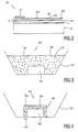
- a light-emitting device 30 includes a light-emitting semiconductor device 32 disposed in a reflective cup 34.
- Reflective cup 34 also contains a material 36 that is substantially transparent to light emitted by device 32.
- Nanoparticles 38 having an index of refraction greater than that of material 36 at wavelengths of light emitted by device 32 are dispersed in substantially transparent material 36.
- Nanoparticles 38 are selected to have diameters less than about a wavelength (e.g., a peak wavelength) of light emitted by device 32 and hence do not substantially scatter the emitted light.
- nanoparticles 38 have diameters less than about 1 ⁇ 4 of a peak emission wavelength of device 32.
- nanoparticles 38 have diameters of about 2 nm to about 50 nm and device 32 emits light having wavelengths greater than about 400 nm.
- Reflective cup 34 reflects light emitted by light-emitting semiconductor device 32 to form an optical output of light-emitting device 30.
- optional phosphor particles 40 shown in Fig. 3 are also dispersed in material 36.
- substantially transparent is used herein to indicate that a material so described transmits light at a peak wavelength emitted by device 32 with less than about 25%, preferably less than about 10%, more preferably less than about 2%, single pass loss due to absorption or scattering.
- Material 36 may be organic or inorganic and may comprise, for example, materials including but not limited to conventional epoxies, acrylic polymers, polycarbonates, silicone polymers, optical glasses, chalcogenide glasses, spiro compounds, and mixtures thereof.
- nanoparticles 38 do not substantially absorb light at wavelengths emitted by device 32, particularly at peak emission wavelengths.
- the phrases "not substantially absorb” and “not substantially absorbing” are used herein to indicate that the nanoparticles in such implementations are sufficiently non-absorbing that they do not increase the single pass loss of light transmitted by the encapsulant to more than about 30%, preferably not to more than about 20%.
- the loss due to absorption by the nanoparticles of light emitted by device 32 will depend on the absorption cross-sections of the individual nanoparticles, the concentration of the nanoparticles in substantially transparent material 36, and possibly on interactions between the nanoparticles and the surrounding material.
- Suitable nanoparticles for such implementations may include, but are not limited to, nanoparticles of metal oxides, nitrides, nitridosilicates, and mixtures thereof.
- Suitable metal oxides may include, but are not limited to, calcium oxide, cerium oxide, hafnium oxide, titanium oxide, zinc oxide, zirconium oxide, and combinations thereof. Nanoparticles of such metal oxides having sizes ranging, for example, from about 2 nm to about 10 run are available, for example, from Degussa-Huls AG of Frankfurt/Main Germany.
- Suitable nanoparticles for such implementations may also include nanoparticles of II-VI semiconductors such as zinc sulfide, zinc selenide, cadmium sulfide, cadmium selenide, cadmium telluride, and their ternary or quaternary mixtures, and nanoparticles of III-V semiconductors such as III-nitrides, III-phosphides, and mixtures thereof.
- Such semiconductor nanoparticles have size tunable absorption spectra, as disclosed, for example, in U.S. Patent Application Serial No. 09/167,795 and in U.S. Patent Application Serial No. 09/350,956.
- the sizes of the semiconductor nanoparticles may be chosen such that the nanoparticles do not substantially absorb at wavelengths emitted by device 32.
- nanoparticles 38 absorb at least a portion of the primary light emitted by light-emitting semiconductor device 32 and emit secondary light of either longer or shorter wavelength than the absorbed light.
- nanoparticles 38 act as phosphors.
- Suitable nanoparticles for such implementations may include, but are not limited to, nanoparticles of the II-VI and III-V materials listed above with sizes chosen such that the nanoparticles absorb a portion of the primary light.
- nanoparticles 38 may be dispersed in material 36 with conventional mixing techniques used in fabricating conventional phosphor converted light-emitting devices and well known to one of ordinary skill in the art.
- a conventional three roll mill may be used to disperse nanoparticles in a silicone material.
- nanoparticles may be dispersed in chalcogenide and optical glasses, for example, by heating the glass to a molten state, adding the nanoparticles as a powder, and stirring the mixture using methods conventional in the glass making arts.
- some semiconductor nanoparticles may be grown or synthesized in a glass by conventional glass-making techniques used in the fabrication of color glass filters.
- the volume fraction (concentration) of nanoparticles 38 in material 36 may be chosen in some implementations such that nanoparticles 38 together with material 36 provide a medium having a particular refractive index.
- the approximate volume fraction of nanoparticles 38 in material 36 needed to provide a desired refractive index may be determined using effective medium theory as explained above.
- the volume fraction of nanoparticles 38 in material 36 may then be varied around the calculated value to determine the volume fraction that provides a mixture having the particular desired refractive index.
- the volume fraction of nanoparticles 38 in material 36 may vary from about 20% to about 60%.
- nanoparticles 38 together with material 36 may provide a medium having a refractive index greater than about 1.6, preferably greater than about 1.8, at a peak wavelength of the primary emission from light-emitting semiconductor device 32, for example.
- material 36 and nanoparticles 38 may be disposed in reflective cup 34 by a variety of well known methods.
- Light extraction from light-emitting semiconductor device 32 may be advantageously increased compared to that for a similar light-emitting device encapsulated in material 36 because the increased refractive index of the mixture of nanoparticles 38 and material 36 may decrease losses due to total internal reflection at the interfaces of device 32 and material 36. This increase in light extraction from device 32 may be accomplished without increasing scattering of the emitted light.
- nanoparticles 38 may advantageously phosphor convert all of or a portion of the primary emission from semiconductor light-emitting device 32 to provide a desired total emission from light-emitting device 30.
- nanoparticles 38 and their volume fraction in material 36 may be chosen by conventional methods used in fabricating phosphor converted light-emitting devices such that the emission from nanoparticles 38 combines with unabsorbed emission from device 32 to provide white light. If necessary, mixing of primary emission from device 32 and secondary emission from nanoparticles 38 may be facilitated, for example, by roughening a surface of any element of light-emitting device 30.
- additional phosphor particles 40 are dispersed in material 36.
- phosphor particles 40 have a refractive index greater than that of material 36 at wavelengths of light emitted by light-emitting semiconductor device 32.
- Phosphor particles 40 may be dispersed in material 36 in combination with nanoparticles 38 that do not substantially absorb light emitted by device 32 or in combination with nanoparticles 38 that absorb a portion of the light emitted by device 32 and emit secondary light.
- phosphor particles 40 have diameters greater than about a wavelength (e.g., a peak wavelength) of light emitted by device 32.
- Suitable phosphor particles for such implementations include, but are not limited to, particles of materials comprising yttrium aluminum garnets, sulfur substituted gallates, unsubstituted gallates, sulfur substituted aluminates, unsubstituted aluminates, phosphates, silicates (nitridosilicates, for example), selenides, sulfides, and mixtures thereof. These materials may be doped with (activated by), for example, rare earth ions including but not limited to cerium and europium ions.
- Phosphor particles 40 may also comprise other conventional phosphor materials known to one of ordinary skill in the art.
- phosphor particles 40 have diameters less than about a wavelength (e.g., a peak wavelength) of light emitted by light-emitting semiconductor device 32.
- Suitable nanoparticles for such implementations may include, but are not limited to, nanoparticles of the II-VI and III-V materials listed above with sizes chosen such that the nanoparticles absorb a portion of the primary light.
- Phosphor particles 40 may also be or include organic dye molecules.
- Phosphor particles 40 may be dispersed in material 36 in combination with nanoparticles 38 by conventional techniques such as those described above. Phosphor 25 particles 40 and their volume fraction in material 36 may be chosen by conventional methods used in fabricating phosphor converted light-emitting devices such that light-emitting device 30 provides a desired output emission spectrum such as, for example, white light.
- the increased refractive index of the mixture of nanoparticles 38 and material 36 compared to that of material 36 alone may advantageously decrease light scattering by and increase light extraction from phosphor particles 40.
- the refractive index of the mixture approaches that of phosphor particles 40, light scattering by the phosphor particles decreases toward zero and light extraction from the phosphor particles is optimized.
- nanoparticles 38 and their volume fraction in material 36 may be chosen such that nanoparticles 38 and material 36 together provide a medium having a refractive index at a wavelength (e.g. a peak wavelength) of emission from device 32 or from phosphor particles 40 that approximately matches the refractive index of phosphor particles 40 at the same wavelength.
- a wavelength e.g. a peak wavelength
- the choice of nanoparticles 38 and their volume fraction in material 36 may be guided by effective medium theory similarly to as explained above.
- the refractive index of a mixture of silicone and cerium oxide or titanium oxide nanoparticles may be adjusted as described above to match that of YAG based phosphor particles to within about 10% to about 2% or better.
- the refractive index of the mixture of nanoparticles 38 and material 36 or the size of phosphor particles 40 may be adjusted so as to provide a desired amount of light scattering by phosphor particles 40.
- the refractive index of the mixture is adjusted so that light scattering by phosphor particles 40 is set to a minimum level needed to facilitate mixing of light emitted by light-emitting semiconductor device 32, phosphor particles 40, and (optionally) nanoparticles 38.
- a light-emitting device 42 includes a light-emitting semiconductor device 32 disposed in a reflective cup 34, and a layer 44 of material 36 disposed on one or more surface of device 32. Nanoparticles 38 and, optionally, phosphor particles 40 are dispersed in material 36. Material 36, nanoparticles 38, and phosphor particles 40 may be provided, for example, in any of the combinations described above with respect to light-emitting device 30 (Fig. 3). Similarly, the incorporation of nanoparticles 38 into light-emitting device 42 may provide any of the previously described advantages.
- Layer 44 may be deposited, for example, by conventional spraying, screen printing, and dipping methods.
- layer 44 may be a conformal layer applied with a stenciling method described in U.S. Patent Application Serial No. 09/688,053 incorporated herein by reference in its entirety.
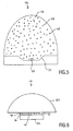
- material 36 is formed into a lens (or other optical element) as shown or provided in, for example, a hollow shell shaped as a lens or other optical element and disposed around light-emitting device 32.
- Material 36, nanoparticles 38, and (optional) phosphor particles 40 may be provided, for example, in any of the combinations described above.
- Material 36 may be formed into a lens or other shape using conventional encapsulation methods familiar to one of ordinary skill in the art.
- the lens shaped portion of light-emitting device 46 reduces losses due to total internal reflection and, in combination with reflector 34, forms an optical output of light-emitting device 46.
- a lens or other optical element 50 is attached to a light-emitting semiconductor device 32 with a layer 52 of material 36.
- Nanoparticles 38, and (optional) phosphor particles 40 may be dispersed in material 36, for example, in any of the combinations described above.
- material 36 is a high refractive index glass having a relatively low melting point
- optical element 50 is bonded to light-emitting semiconductor device 32 with layer 52 by a wafer-bonding method such as, for example, those disclosed in U.S. Patent Application Serial No. 09/660,317, incorporated herein by reference in its entirety.
- optical element 50 may be advantageously formed.
- Light extraction from light-emitting semiconductor device 32 may be advantageously increased by forming optical element 50 from a material having a relatively high refractive index.
- Fig. 7 is an exploded view of a packaged light-emitting device in accordance with some embodiments.
- Light-emitting device 54 which may be any of the light-emitting devices described herein or a light-emitting semiconductor device component of such a light-emitting device, is mounted directly or indirectly via a thermally conducting submount 56 to a heat-sinking slug 58.
- Slug 58 may include an optional reflector cup 60, which may be in addition to or substitute for reflector 34 (Figs. 3-5).
- Slug 58 is placed into an insert-molded leadframe 62.
- Insert-molded leadframe 62 is, for example, a filled plastic material molded around a metal frame that provides an electrical path to light-emitting device 54.
- a lens 64 or other optical element may be added. Lens 64 may be in addition to or substitute for the lenses shown in Figs. 5 and 6.
- nanoparticles may be employed as described above to reduce scattering by phosphor particles of light provided by light sources other than light-emitting semiconductor devices, and to improve light extraction from such lightsources.
- Alternative light sources include, for example, lasers, conventional incandescent lamps, and fluorescent lamps.
- material 36 including nanoparticles 38 and (optionally) phosphor particles 40 is shown in the Figures as disposed directly on light-emitting semiconductor device 32, in other embodiments material 36 may be spaced apart from device 32.
- material 36 may be spaced apart from device 32 by a transparent spacer layer as disclosed in U.S. Patent No. 5,959,316, incorporated herein by reference in its entirety.
- the embodiments illustrated in Figs. 3-5 each include a reflector 34, some other embodiments do not include such a reflector.
- lenses employed in several embodiments have been illustrated as dome-shaped, such lenses may have other shapes or may be implemented, for example, with a microlens array.
Applications Claiming Priority (2)
| Application Number | Priority Date | Filing Date | Title |
|---|---|---|---|
| US165571 | 1993-12-15 | ||
| US10/165,571 US6870311B2 (en) | 2002-06-07 | 2002-06-07 | Light-emitting devices utilizing nanoparticles |
Publications (2)
| Publication Number | Publication Date |
|---|---|
| EP1369935A1 true EP1369935A1 (fr) | 2003-12-10 |
| EP1369935B1 EP1369935B1 (fr) | 2019-08-07 |
Family
ID=29549380
Family Applications (1)
| Application Number | Title | Priority Date | Filing Date |
|---|---|---|---|
| EP03076772.7A Expired - Lifetime EP1369935B1 (fr) | 2002-06-07 | 2003-06-05 | LED contenant des nanoparticules |
Country Status (6)
| Country | Link |
|---|---|
| US (2) | US6870311B2 (fr) |
| EP (1) | EP1369935B1 (fr) |
| JP (1) | JP4666891B2 (fr) |
| AU (1) | AU2003232393A1 (fr) |
| TW (1) | TWI307969B (fr) |
| WO (1) | WO2003105242A1 (fr) |
Cited By (29)
| Publication number | Priority date | Publication date | Assignee | Title |
|---|---|---|---|---|
| WO2005008789A3 (fr) * | 2003-07-14 | 2005-06-16 | Osram Opto Semiconductors Gmbh | Composant emettant de la lumiere, pourvu d'un element de conversion de luminescence |
| WO2005067524A2 (fr) | 2004-01-15 | 2005-07-28 | Nanosys, Inc. | Matrices dopees avec des nanocristaux |
| WO2006061729A2 (fr) * | 2004-12-06 | 2006-06-15 | Philips Intellectual Property & Standards Gmbh | Source lumineuse electroluminescente organique |
| DE102005045106A1 (de) * | 2004-12-10 | 2006-06-29 | Agilent Technologies, Inc. (n.d.Ges.d.Staates Delaware), Palo Alto | Blitzmodul mit Quantenpunktlichtumwandlung |
| WO2006122524A1 (fr) * | 2005-05-19 | 2006-11-23 | Patent-Treuhand-Gesellschaft für elektrische Glühlampen mbH | Diode electroluminescente a conversion de luminescence |
| WO2007002234A1 (fr) * | 2005-06-23 | 2007-01-04 | Rensselaer Polytechnic Institute | Conception de conditionnement produisant une lumière blanche avec des dels de faible longueur d’onde et matériaux de conversion de réduction |
| WO2007006246A1 (fr) * | 2005-06-23 | 2007-01-18 | Osram Opto Semiconductors Gmbh | Materiau convertisseur de longueur d'onde, composant optique electroluminescent et son procede de production |
| WO2008018003A2 (fr) * | 2006-08-08 | 2008-02-14 | Koninklijke Philips Electronics N.V. | Nanoparticule à base de matériau de liaison inorganique |
| US7385349B2 (en) | 2004-01-07 | 2008-06-10 | Koito Manufacturing Co., Ltd. | Light emitting module and lighting unit for vehicle |
| EP1950239A1 (fr) * | 2005-10-28 | 2008-07-30 | Sumitomo Osaka Cement Co., Ltd. | Dispersion transparente d oxyde inorganique, composition de resine contenant des particules d oxyde inorganique, composition pour encapsuler un element luminescent, element luminescent, revetement dur, film fonctionnel optique, piece optique et procede de production d une composition de resine contenant des particules d'oxide inorganique |
| US7470974B2 (en) | 2006-07-14 | 2008-12-30 | Cabot Corporation | Substantially transparent material for use with light-emitting device |
| DE102007049005A1 (de) * | 2007-09-11 | 2009-03-12 | Osram Opto Semiconductors Gmbh | Strahlungsemittierende Vorrichtung |
| EP2042528A1 (fr) * | 2007-09-25 | 2009-04-01 | Sony Chemical & Information Device Corporation | Composition de résine durcissable |
| US7522211B2 (en) | 2005-02-10 | 2009-04-21 | Avago Technologies Ecbu Ip (Singapore) Pte. Ltd. | Studio light |
| WO2006054233A3 (fr) * | 2004-11-19 | 2009-04-30 | Koninkl Philips Electronics Nv | Dispositif electroluminescent comprenant un boitier inorganique |
| US7667766B2 (en) | 2003-12-18 | 2010-02-23 | Avago Technologies Ecbu Ip (Singapore) Pte. Ltd. | Adjustable spectrum flash lighting for image acquisition |
| WO2010038097A1 (fr) * | 2008-10-01 | 2010-04-08 | Koninklijke Philips Electronics N.V. | Diode électroluminescente avec particules dans un encapsulant afin d’améliorer l’extraction de lumière et la couleur non jaune à l’état arrêté |
| EP1755174A3 (fr) * | 2005-08-16 | 2010-08-25 | Kabushiki Kaisha Toshiba | Dispositif luminescent |
| US7791093B2 (en) | 2007-09-04 | 2010-09-07 | Koninklijke Philips Electronics N.V. | LED with particles in encapsulant for increased light extraction and non-yellow off-state color |
| US7879258B2 (en) | 2005-03-14 | 2011-02-01 | Koninklijke Philips Electronics N.V. | Phosphor in polycrystalline ceramic structure and a light-emitting element comprising same |
| EP2113949A3 (fr) * | 2008-05-02 | 2011-09-21 | Cree, Inc. | Encapsulation pour diode électroluminescente blanche à conversion par phosphore |
| US8227817B2 (en) | 2006-12-22 | 2012-07-24 | Qunano Ab | Elevated LED |
| US8415692B2 (en) | 2009-07-06 | 2013-04-09 | Cree, Inc. | LED packages with scattering particle regions |
| US8425803B2 (en) | 2004-01-15 | 2013-04-23 | Samsung Electronics Co., Ltd. | Nanocrystal doped matrixes |
| CN103563108A (zh) * | 2012-05-22 | 2014-02-05 | 松下电器产业株式会社 | 波长变换元件及其制造方法和使用波长变换元件的led元件及半导体激光发光装置 |
| US9273830B2 (en) | 2007-06-14 | 2016-03-01 | Cree, Inc. | Light source with near field mixing |
| DE102015102842A1 (de) | 2015-02-27 | 2016-09-01 | Fraunhofer-Gesellschaft zur Förderung der angewandten Forschung e.V. | Leuchtstoffkompositkeramik sowie Verfahren zu deren Herstellung |
| EP1864274B1 (fr) * | 2005-03-25 | 2019-04-24 | Arkema France | Dispositif d'eclairage combinant une del et une feuille de diffusion |
| US11114594B2 (en) | 2007-08-24 | 2021-09-07 | Creeled, Inc. | Light emitting device packages using light scattering particles of different size |
Families Citing this family (220)
| Publication number | Priority date | Publication date | Assignee | Title |
|---|---|---|---|---|
| US7053419B1 (en) | 2000-09-12 | 2006-05-30 | Lumileds Lighting U.S., Llc | Light emitting diodes with improved light extraction efficiency |
| JP2002141556A (ja) | 2000-09-12 | 2002-05-17 | Lumileds Lighting Us Llc | 改良された光抽出効果を有する発光ダイオード |
| US6744077B2 (en) * | 2002-09-27 | 2004-06-01 | Lumileds Lighting U.S., Llc | Selective filtering of wavelength-converted semiconductor light emitting devices |
| US8993221B2 (en) | 2012-02-10 | 2015-03-31 | Pixelligent Technologies, Llc | Block co-polymer photoresist |
| JP2006523383A (ja) | 2003-03-04 | 2006-10-12 | ピクセリジェント・テクノロジーズ・エルエルシー | フォトリソグラフィ用のナノサイズ半導体粒子の応用 |
| US20040252488A1 (en) * | 2003-04-01 | 2004-12-16 | Innovalight | Light-emitting ceiling tile |
| US7279832B2 (en) * | 2003-04-01 | 2007-10-09 | Innovalight, Inc. | Phosphor materials and illumination devices made therefrom |
| US20070013057A1 (en) * | 2003-05-05 | 2007-01-18 | Joseph Mazzochette | Multicolor LED assembly with improved color mixing |
| WO2004104646A1 (fr) * | 2003-05-20 | 2004-12-02 | Kansas State University Research Foundation | Microlentille comportant une matiere a base d'un nitrure du groupe iii |
| US7321714B2 (en) * | 2003-06-13 | 2008-01-22 | Ers Company | Moisture-resistant nano-particle material and its applications |
| US7009213B2 (en) * | 2003-07-31 | 2006-03-07 | Lumileds Lighting U.S., Llc | Light emitting devices with improved light extraction efficiency |
| JP2005064233A (ja) * | 2003-08-12 | 2005-03-10 | Stanley Electric Co Ltd | 波長変換型led |
| JP2005093712A (ja) * | 2003-09-17 | 2005-04-07 | Stanley Electric Co Ltd | 半導体発光装置 |
| DE10345157B4 (de) * | 2003-09-29 | 2009-01-08 | Qimonda Ag | Wärmeleitende Verpackung von elektronischen Schaltungseinheiten |
| US7307286B2 (en) * | 2003-10-16 | 2007-12-11 | Nitto Denko Corporation | Epoxy resin composition for encapsulating optical semiconductor element and optical semiconductor device using the same |
| CA2544129A1 (fr) * | 2003-10-22 | 2005-05-06 | The Regents Of The University Of California | Procedes de preparation et nanoparticules de fonctionnalisation |
| DE10351397A1 (de) * | 2003-10-31 | 2005-06-16 | Osram Opto Semiconductors Gmbh | Lumineszenzdiodenchip |
| JP4590905B2 (ja) * | 2003-10-31 | 2010-12-01 | 豊田合成株式会社 | 発光素子および発光装置 |
| DE10351349A1 (de) | 2003-10-31 | 2005-06-16 | Osram Opto Semiconductors Gmbh | Verfahren zum Hestellen eines Lumineszenzdiodenchips |
| JP4784966B2 (ja) * | 2003-11-18 | 2011-10-05 | シャープ株式会社 | 半導体レーザ装置および照明装置 |
| US7102152B2 (en) * | 2004-10-14 | 2006-09-05 | Avago Technologies Ecbu Ip (Singapore) Pte. Ltd. | Device and method for emitting output light using quantum dots and non-quantum fluorescent material |
| TWI236162B (en) * | 2003-12-26 | 2005-07-11 | Ind Tech Res Inst | Light emitting diode |
| US20050167684A1 (en) * | 2004-01-21 | 2005-08-04 | Chua Janet B.Y. | Device and method for emitting output light using group IIB element selenide-based phosphor material |
| US20050269932A1 (en) * | 2004-01-21 | 2005-12-08 | Ng Kee Y | Apparatus, device and method for emitting output light using group IIB element selenide-based phosphor material and/or thiogallate-based phosphor material |
| US20050156510A1 (en) * | 2004-01-21 | 2005-07-21 | Chua Janet B.Y. | Device and method for emitting output light using group IIB element selenide-based and group IIA element gallium sulfide-based phosphor materials |
| CN100446279C (zh) * | 2004-02-18 | 2008-12-24 | 财团法人工业技术研究院 | 发光二极管 |
| US7868343B2 (en) * | 2004-04-06 | 2011-01-11 | Cree, Inc. | Light-emitting devices having multiple encapsulation layers with at least one of the encapsulation layers including nanoparticles and methods of forming the same |
| US7553683B2 (en) * | 2004-06-09 | 2009-06-30 | Philips Lumiled Lighting Co., Llc | Method of forming pre-fabricated wavelength converting elements for semiconductor light emitting devices |
| US7534633B2 (en) * | 2004-07-02 | 2009-05-19 | Cree, Inc. | LED with substrate modifications for enhanced light extraction and method of making same |
| US20060006397A1 (en) * | 2004-07-09 | 2006-01-12 | Chua Janet B Y | Device and method for emitting output light using group IIA/IIB selenide sulfur-based phosphor material |
| US7750352B2 (en) | 2004-08-10 | 2010-07-06 | Pinion Technologies, Inc. | Light strips for lighting and backlighting applications |
| JP4786886B2 (ja) * | 2004-08-11 | 2011-10-05 | ローム株式会社 | 半導体発光装置 |
| US7471040B2 (en) * | 2004-08-13 | 2008-12-30 | Avago Technologies Ecbu Ip (Singapore) Pte. Ltd. | Mixed-color light emitting diode apparatus, and method for making same |
| KR100668609B1 (ko) * | 2004-09-24 | 2007-01-16 | 엘지전자 주식회사 | 백색광원소자 |
| TWI256149B (en) * | 2004-09-27 | 2006-06-01 | Advanced Optoelectronic Tech | Light apparatus having adjustable color light and manufacturing method thereof |
| US7265488B2 (en) * | 2004-09-30 | 2007-09-04 | Avago Technologies General Ip Pte. Ltd | Light source with wavelength converting material |
| WO2006040704A1 (fr) * | 2004-10-12 | 2006-04-20 | Philips Intellectual Property & Standards Gmbh | Source de lumiere electroluminescente |
| US20060091414A1 (en) * | 2004-10-29 | 2006-05-04 | Ouderkirk Andrew J | LED package with front surface heat extractor |
| US9929326B2 (en) | 2004-10-29 | 2018-03-27 | Ledengin, Inc. | LED package having mushroom-shaped lens with volume diffuser |
| US8324641B2 (en) * | 2007-06-29 | 2012-12-04 | Ledengin, Inc. | Matrix material including an embedded dispersion of beads for a light-emitting device |
| US7304425B2 (en) * | 2004-10-29 | 2007-12-04 | 3M Innovative Properties Company | High brightness LED package with compound optical element(s) |
| US8134292B2 (en) * | 2004-10-29 | 2012-03-13 | Ledengin, Inc. | Light emitting device with a thermal insulating and refractive index matching material |
| US8816369B2 (en) | 2004-10-29 | 2014-08-26 | Led Engin, Inc. | LED packages with mushroom shaped lenses and methods of manufacturing LED light-emitting devices |
| US7419839B2 (en) | 2004-11-12 | 2008-09-02 | Philips Lumileds Lighting Company, Llc | Bonding an optical element to a light emitting device |
| US7462502B2 (en) | 2004-11-12 | 2008-12-09 | Philips Lumileds Lighting Company, Llc | Color control by alteration of wavelength converting element |
| ATE527705T1 (de) * | 2004-12-06 | 2011-10-15 | Koninkl Philips Electronics Nv | Organische elektrolumineszente lichtquelle |
| US7602116B2 (en) * | 2005-01-27 | 2009-10-13 | Advanced Optoelectronic Technology, Inc. | Light apparatus capable of emitting light of multiple wavelengths using nanometer fluorescent material, light device and manufacturing method thereof |
| US7341878B2 (en) * | 2005-03-14 | 2008-03-11 | Philips Lumileds Lighting Company, Llc | Wavelength-converted semiconductor light emitting device |
| KR100682874B1 (ko) * | 2005-05-02 | 2007-02-15 | 삼성전기주식회사 | 백색 led |
| JP2006310710A (ja) | 2005-05-02 | 2006-11-09 | Sony Corp | 半導体発光素子 |
| US8487527B2 (en) * | 2005-05-04 | 2013-07-16 | Lg Display Co., Ltd. | Organic light emitting devices |
| US7777407B2 (en) | 2005-05-04 | 2010-08-17 | Lg Display Co., Ltd. | Organic light emitting devices comprising a doped triazine electron transport layer |
| US7868302B2 (en) * | 2005-05-05 | 2011-01-11 | Board Of Regents Of The University Of Nebraska | Nano-particle/quantum dot based optical diode |
| KR101111747B1 (ko) * | 2005-05-16 | 2012-06-12 | 삼성엘이디 주식회사 | 혼합 나노 입자 및 이를 이용한 전자소자 |
| US7795806B2 (en) | 2005-05-20 | 2010-09-14 | Lg Display Co., Ltd. | Reduced reflectance display devices containing a thin-layer metal-organic mixed layer (MOML) |
| US7943244B2 (en) * | 2005-05-20 | 2011-05-17 | Lg Display Co., Ltd. | Display device with metal-organic mixed layer anodes |
| US7728517B2 (en) * | 2005-05-20 | 2010-06-01 | Lg Display Co., Ltd. | Intermediate electrodes for stacked OLEDs |
| US7811679B2 (en) * | 2005-05-20 | 2010-10-12 | Lg Display Co., Ltd. | Display devices with light absorbing metal nanoparticle layers |
| US7750561B2 (en) * | 2005-05-20 | 2010-07-06 | Lg Display Co., Ltd. | Stacked OLED structure |
| US8718437B2 (en) | 2006-03-07 | 2014-05-06 | Qd Vision, Inc. | Compositions, optical component, system including an optical component, devices, and other products |
| US9297092B2 (en) | 2005-06-05 | 2016-03-29 | Qd Vision, Inc. | Compositions, optical component, system including an optical component, devices, and other products |
| EP2075288B1 (fr) * | 2005-06-14 | 2014-09-03 | Denki Kagaku Kogyo Kabushiki Kaisha | Composition de résine et feuille contenant du phosphore, et élément d'émission lumineuse utilisant une telle composition et feuille |
| KR101161383B1 (ko) * | 2005-07-04 | 2012-07-02 | 서울반도체 주식회사 | 발광 다이오드 및 이를 제조하기 위한 방법 |
| KR101106134B1 (ko) * | 2005-07-11 | 2012-01-20 | 서울옵토디바이스주식회사 | 나노와이어 형광체를 채택한 발광소자 |
| CN101223824B (zh) * | 2005-07-14 | 2011-05-18 | 皇家飞利浦电子股份有限公司 | 场致发光器件 |
| JP4778745B2 (ja) * | 2005-07-27 | 2011-09-21 | パナソニック株式会社 | 半導体発光装置及びその製造方法 |
| US20070023762A1 (en) * | 2005-07-29 | 2007-02-01 | Luxo Asa And Oec Ag | White light emitting LED-powered lamp |
| KR20080049011A (ko) * | 2005-08-05 | 2008-06-03 | 마쯔시다덴기산교 가부시키가이샤 | 반도체 발광장치 |
| US8187726B2 (en) * | 2005-08-09 | 2012-05-29 | Sony Corporation | Nanoparticle-resin composite material, light emitting device assembly, and filling material for the light-emitting device assembly |
| JP4415972B2 (ja) * | 2005-09-22 | 2010-02-17 | ソニー株式会社 | 金属酸化物ナノ粒子の製造方法 |
| US7594845B2 (en) * | 2005-10-20 | 2009-09-29 | 3M Innovative Properties Company | Abrasive article and method of modifying the surface of a workpiece |
| JP2007299981A (ja) * | 2006-05-01 | 2007-11-15 | Sumitomo Osaka Cement Co Ltd | 発光素子封止用組成物及び発光素子並びに光半導体装置 |
| US20070116423A1 (en) * | 2005-11-22 | 2007-05-24 | 3M Innovative Properties Company | Arrays of optical elements and method of manufacturing same |
| US20070196657A1 (en) * | 2005-12-15 | 2007-08-23 | Cabot Corporation | Transparent polymer composites |
| US7772604B2 (en) * | 2006-01-05 | 2010-08-10 | Illumitex | Separate optical device for directing light from an LED |
| CN101361202B (zh) | 2006-01-16 | 2010-12-08 | 松下电器产业株式会社 | 半导体发光装置 |
| US8044412B2 (en) | 2006-01-20 | 2011-10-25 | Taiwan Semiconductor Manufacturing Company, Ltd | Package for a light emitting element |
| KR100867519B1 (ko) * | 2006-02-02 | 2008-11-07 | 삼성전기주식회사 | 발광 다이오드 모듈 |
| US9951438B2 (en) | 2006-03-07 | 2018-04-24 | Samsung Electronics Co., Ltd. | Compositions, optical component, system including an optical component, devices, and other products |
| US8849087B2 (en) * | 2006-03-07 | 2014-09-30 | Qd Vision, Inc. | Compositions, optical component, system including an optical component, devices, and other products |
| US9874674B2 (en) | 2006-03-07 | 2018-01-23 | Samsung Electronics Co., Ltd. | Compositions, optical component, system including an optical component, devices, and other products |
| EP2041478B1 (fr) | 2006-03-07 | 2014-08-06 | QD Vision, Inc. | Objet contenant des nanocristaux semi-conducteurs |
| JP2007277467A (ja) | 2006-04-10 | 2007-10-25 | Sony Chemical & Information Device Corp | 硬化性樹脂組成物 |
| US8141384B2 (en) * | 2006-05-03 | 2012-03-27 | 3M Innovative Properties Company | Methods of making LED extractor arrays |
| US7423297B2 (en) * | 2006-05-03 | 2008-09-09 | 3M Innovative Properties Company | LED extractor composed of high index glass |
| US8941293B2 (en) * | 2006-05-11 | 2015-01-27 | Samsung Electronics Co., Ltd. | Solid state lighting devices comprising quantum dots |
| US20090256167A1 (en) * | 2006-06-08 | 2009-10-15 | Koninklijke Philips Electronics N.V. | Light-emitting device |
| KR100901947B1 (ko) * | 2006-07-14 | 2009-06-10 | 삼성전자주식회사 | 반도체 나노결정을 이용하는 백색 발광 다이오드 및 그의제조방법 |
| US20100224890A1 (en) * | 2006-09-18 | 2010-09-09 | Cree, Inc. | Light emitting diode chip with electrical insulation element |
| KR20090064474A (ko) * | 2006-10-02 | 2009-06-18 | 일루미텍스, 인크. | Led 시스템 및 방법 |
| US20090275266A1 (en) * | 2006-10-02 | 2009-11-05 | Illumitex, Inc. | Optical device polishing |
| TWI338380B (en) * | 2006-10-11 | 2011-03-01 | Chuan Yu Hung | Light emitting diode incorporating high refractive index material |
| JP4952906B2 (ja) | 2006-11-15 | 2012-06-13 | ソニーケミカル&インフォメーションデバイス株式会社 | 封止樹脂組成物及び発光素子 |
| WO2008063658A2 (fr) * | 2006-11-21 | 2008-05-29 | Qd Vision, Inc. | Nanocristaux à semi-conducteurs et compositions et dispositifs contenant ceux-ci |
| WO2008063652A1 (fr) | 2006-11-21 | 2008-05-29 | Qd Vision, Inc. | Nanocristaux à semi-conducteurs émettant une lumière bleue et compositions et dispositifs contenant ceux-ci |
| TW201448263A (zh) | 2006-12-11 | 2014-12-16 | Univ California | 透明發光二極體 |
| JP4315195B2 (ja) * | 2006-12-21 | 2009-08-19 | ソニー株式会社 | 硬化性樹脂材料−微粒子複合材料及びその製造方法、光学材料、並びに発光装置 |
| US8951631B2 (en) | 2007-01-03 | 2015-02-10 | Applied Nanostructured Solutions, Llc | CNT-infused metal fiber materials and process therefor |
| US8951632B2 (en) | 2007-01-03 | 2015-02-10 | Applied Nanostructured Solutions, Llc | CNT-infused carbon fiber materials and process therefor |
| US9005755B2 (en) | 2007-01-03 | 2015-04-14 | Applied Nanostructured Solutions, Llc | CNS-infused carbon nanomaterials and process therefor |
| US8836212B2 (en) | 2007-01-11 | 2014-09-16 | Qd Vision, Inc. | Light emissive printed article printed with quantum dot ink |
| US8021904B2 (en) * | 2007-02-01 | 2011-09-20 | Cree, Inc. | Ohmic contacts to nitrogen polarity GaN |
| ITTO20070099A1 (it) * | 2007-02-09 | 2008-08-10 | St Microelectronics Srl | Procedimento per la realizzazione di un'interfaccia tra carburo di silicio e ossido di silicio con bassa densita' di stati |
| DE102007010719A1 (de) * | 2007-03-06 | 2008-09-11 | Merck Patent Gmbh | Leuchtstoffe bestehend aus dotierten Granaten für pcLEDs |
| US8941566B2 (en) * | 2007-03-08 | 2015-01-27 | 3M Innovative Properties Company | Array of luminescent elements |
| EP2121872B1 (fr) * | 2007-03-19 | 2015-12-09 | Nanosys, Inc. | Procédés pour encapsuler des nanocristaux |
| US20100110728A1 (en) | 2007-03-19 | 2010-05-06 | Nanosys, Inc. | Light-emitting diode (led) devices comprising nanocrystals |
| US20100155749A1 (en) * | 2007-03-19 | 2010-06-24 | Nanosys, Inc. | Light-emitting diode (led) devices comprising nanocrystals |
| KR100900866B1 (ko) * | 2007-05-09 | 2009-06-04 | 삼성전자주식회사 | 나노결정-금속산화물 복합체를 이용하는 발광 다이오드소자 및 그의 제조방법 |
| US7999283B2 (en) * | 2007-06-14 | 2011-08-16 | Cree, Inc. | Encapsulant with scatterer to tailor spatial emission pattern and color uniformity in light emitting diodes |
| JP5773646B2 (ja) | 2007-06-25 | 2015-09-02 | キユーデイー・ビジヨン・インコーポレーテツド | ナノ材料を被着させることを含む組成物および方法 |
| TWI365546B (en) * | 2007-06-29 | 2012-06-01 | Ind Tech Res Inst | Light emitting diode device and fabrication method thereof |
| WO2009014707A2 (fr) | 2007-07-23 | 2009-01-29 | Qd Vision, Inc. | Substrat d'amélioration de lumière à point quantique et dispositif d'éclairage le comprenant |
| WO2009026105A1 (fr) * | 2007-08-17 | 2009-02-26 | Massachusetts Institute Of Technology | Matériau électroluminescent |
| US8128249B2 (en) * | 2007-08-28 | 2012-03-06 | Qd Vision, Inc. | Apparatus for selectively backlighting a material |
| US8519437B2 (en) * | 2007-09-14 | 2013-08-27 | Cree, Inc. | Polarization doping in nitride based diodes |
| US7446159B1 (en) | 2007-09-20 | 2008-11-04 | Sony Corporation | Curable resin composition |
| US20090085463A1 (en) * | 2007-09-28 | 2009-04-02 | General Electric Company | Thermo-optically functional compositions, systems and methods of making |
| US9012937B2 (en) | 2007-10-10 | 2015-04-21 | Cree, Inc. | Multiple conversion material light emitting diode package and method of fabricating same |
| CN101414651B (zh) * | 2007-10-17 | 2010-06-16 | 洪绢欲 | 以高折光率纳米粒子堆积所装置之发光二极管组件及其制造方法 |
| US8368100B2 (en) * | 2007-11-14 | 2013-02-05 | Cree, Inc. | Semiconductor light emitting diodes having reflective structures and methods of fabricating same |
| US8294156B2 (en) * | 2007-11-19 | 2012-10-23 | Samsung Electronics Co., Ltd. | Nanocrystal light-emitting diode |
| CN101878540B (zh) | 2007-11-29 | 2013-11-06 | 日亚化学工业株式会社 | 发光装置及其制造方法 |
| US9431589B2 (en) * | 2007-12-14 | 2016-08-30 | Cree, Inc. | Textured encapsulant surface in LED packages |
| US20090154198A1 (en) * | 2007-12-14 | 2009-06-18 | Joo Hoon Lee | Reflection type display apparatus |
| US20090173958A1 (en) * | 2008-01-04 | 2009-07-09 | Cree, Inc. | Light emitting devices with high efficiency phospor structures |
| JP2011512037A (ja) * | 2008-02-08 | 2011-04-14 | イルミテックス, インコーポレイテッド | エミッタ層成形のためのシステムおよび方法 |
| US8169136B2 (en) * | 2008-02-21 | 2012-05-01 | Nitto Denko Corporation | Light emitting device with translucent ceramic plate |
| WO2009145813A1 (fr) | 2008-03-04 | 2009-12-03 | Qd Vision, Inc. | Particules comprenant des nanoparticules, leurs utilisations, et procédés |
| US8877524B2 (en) * | 2008-03-31 | 2014-11-04 | Cree, Inc. | Emission tuning methods and devices fabricated utilizing methods |
| JP2011520244A (ja) * | 2008-04-03 | 2011-07-14 | バンドギャップ エンジニアリング, インコーポレイテッド | 性能を改善するナノ構造の光電子デバイスのホストの設計 |
| DE102008021438A1 (de) | 2008-04-29 | 2009-12-31 | Schott Ag | Konversionsmaterial insbesondere für eine, eine Halbleiterlichtquelle umfassende weiße oder farbige Lichtquelle, Verfahren zu dessen Herstellung sowie dieses Konversionsmaterial umfassende Lichtquelle |
| US9207385B2 (en) | 2008-05-06 | 2015-12-08 | Qd Vision, Inc. | Lighting systems and devices including same |
| WO2009137053A1 (fr) | 2008-05-06 | 2009-11-12 | Qd Vision, Inc. | Composants optiques, systèmes comprenant un composant optique et dispositifs associés |
| JP2011524064A (ja) | 2008-05-06 | 2011-08-25 | キユーデイー・ビジヨン・インコーポレーテツド | 量子閉じ込め半導体ナノ粒子を含有する固体照明装置 |
| JP2011523212A (ja) * | 2008-06-05 | 2011-08-04 | スリーエム イノベイティブ プロパティズ カンパニー | 半導体波長変換器が接合された発光ダイオード |
| US8383432B2 (en) * | 2008-08-07 | 2013-02-26 | Sharp Laboratories Of America, Inc. | Colloidal-processed silicon particle device |
| US7888691B2 (en) * | 2008-08-29 | 2011-02-15 | Koninklijke Philips Electronics N.V. | Light source including a wavelength-converted semiconductor light emitting device and a filter |
| US8075165B2 (en) | 2008-10-14 | 2011-12-13 | Ledengin, Inc. | Total internal reflection lens and mechanical retention and locating device |
| US8096676B2 (en) * | 2008-10-21 | 2012-01-17 | Mitutoyo Corporation | High intensity pulsed light source configurations |
| US20100097779A1 (en) * | 2008-10-21 | 2010-04-22 | Mitutoyo Corporation | High intensity pulsed light source configurations |
| US20100117106A1 (en) * | 2008-11-07 | 2010-05-13 | Ledengin, Inc. | Led with light-conversion layer |
| CA2741864C (fr) * | 2008-11-07 | 2015-12-29 | Idd Aerospace Corporation | Systemes d'eclairage |
| US8360617B2 (en) * | 2008-11-25 | 2013-01-29 | Samsung Electronics Co., Ltd. | Lighting system including LED with glass-coated quantum-dots |
| TW201034256A (en) | 2008-12-11 | 2010-09-16 | Illumitex Inc | Systems and methods for packaging light-emitting diode devices |
| US8507300B2 (en) * | 2008-12-24 | 2013-08-13 | Ledengin, Inc. | Light-emitting diode with light-conversion layer |
| US11198270B2 (en) | 2008-12-30 | 2021-12-14 | Nanosys, Inc. | Quantum dot films, lighting devices, and lighting methods |
| US8343575B2 (en) | 2008-12-30 | 2013-01-01 | Nanosys, Inc. | Methods for encapsulating nanocrystals and resulting compositions |
| US10214686B2 (en) | 2008-12-30 | 2019-02-26 | Nanosys, Inc. | Methods for encapsulating nanocrystals and resulting compositions |
| AU2010257117A1 (en) | 2009-02-27 | 2011-08-11 | Applied Nanostructured Solutions Llc | Low temperature CNT growth using gas-preheat method |
| US20100224129A1 (en) | 2009-03-03 | 2010-09-09 | Lockheed Martin Corporation | System and method for surface treatment and barrier coating of fibers for in situ cnt growth |
| US20100264371A1 (en) * | 2009-03-19 | 2010-10-21 | Nick Robert J | Composition including quantum dots, uses of the foregoing, and methods |
| US8598793B2 (en) | 2011-05-12 | 2013-12-03 | Ledengin, Inc. | Tuning of emitter with multiple LEDs to a single color bin |
| US7985000B2 (en) * | 2009-04-08 | 2011-07-26 | Ledengin, Inc. | Lighting apparatus having multiple light-emitting diodes with individual light-conversion layers |
| US8384097B2 (en) | 2009-04-08 | 2013-02-26 | Ledengin, Inc. | Package for multiple light emitting diodes |
| WO2010126606A2 (fr) | 2009-05-01 | 2010-11-04 | Nanosys, Inc. | Matrices fonctionnalisées pour la dispersion de nanostructures |
| KR101644047B1 (ko) * | 2009-07-09 | 2016-08-01 | 삼성전자 주식회사 | 발광체-고분자 복합체용 조성물, 발광체-고분자 복합체 및 상기 발광체-고분자 복합체를 포함하는 발광 소자 |
| JP5823393B2 (ja) * | 2009-08-03 | 2015-11-25 | アプライド ナノストラクチャード ソリューションズ リミテッド ライアビリティー カンパニーApplied Nanostructuredsolutions, Llc | 複合繊維へのナノ粒子の組み込み |
| EP2465147B1 (fr) | 2009-08-14 | 2019-02-27 | Samsung Electronics Co., Ltd. | Dispositifs d'éclairage, composant optique pour un dispositif d'éclairage et procédés associés |
| US8449128B2 (en) * | 2009-08-20 | 2013-05-28 | Illumitex, Inc. | System and method for a lens and phosphor layer |
| US8585253B2 (en) | 2009-08-20 | 2013-11-19 | Illumitex, Inc. | System and method for color mixing lens array |
| WO2011031876A1 (fr) | 2009-09-09 | 2011-03-17 | Qd Vision, Inc. | Formulations comprenant des nanoparticules |
| CN102482457B (zh) | 2009-09-09 | 2015-04-15 | Qd视光有限公司 | 包含纳米颗粒的颗粒、其应用和方法 |
| US8203161B2 (en) * | 2009-11-23 | 2012-06-19 | Koninklijke Philips Electronics N.V. | Wavelength converted semiconductor light emitting device |
| US8604461B2 (en) * | 2009-12-16 | 2013-12-10 | Cree, Inc. | Semiconductor device structures with modulated doping and related methods |
| US8536615B1 (en) | 2009-12-16 | 2013-09-17 | Cree, Inc. | Semiconductor device structures with modulated and delta doping and related methods |
| US8303141B2 (en) * | 2009-12-17 | 2012-11-06 | Ledengin, Inc. | Total internal reflection lens with integrated lamp cover |
| JP2010098335A (ja) * | 2010-02-01 | 2010-04-30 | Toshiba Corp | 発光装置 |
| KR100969100B1 (ko) | 2010-02-12 | 2010-07-09 | 엘지이노텍 주식회사 | 발광소자, 발광소자의 제조방법 및 발광소자 패키지 |
| JP4980492B2 (ja) | 2010-03-10 | 2012-07-18 | パナソニック株式会社 | Led装置の製造方法 |
| US8530883B2 (en) * | 2010-03-11 | 2013-09-10 | Light-Based Technologies Incorporated | Manufacture of quantum dot-enabled solid-state light emitters |
| KR101683270B1 (ko) | 2010-03-31 | 2016-12-21 | 삼성전자 주식회사 | 백색 발광 다이오드를 포함하는 액정 디스플레이 장치 |
| US9345095B2 (en) | 2010-04-08 | 2016-05-17 | Ledengin, Inc. | Tunable multi-LED emitter module |
| US9080729B2 (en) | 2010-04-08 | 2015-07-14 | Ledengin, Inc. | Multiple-LED emitter for A-19 lamps |
| US8858022B2 (en) | 2011-05-05 | 2014-10-14 | Ledengin, Inc. | Spot TIR lens system for small high-power emitter |
| US20110278536A1 (en) * | 2010-05-17 | 2011-11-17 | Massachusetts Institute Of Technology | Light emitting material |
| US8142050B2 (en) | 2010-06-24 | 2012-03-27 | Mitutoyo Corporation | Phosphor wheel configuration for high intensity point source |
| US9382470B2 (en) | 2010-07-01 | 2016-07-05 | Samsung Electronics Co., Ltd. | Thiol containing compositions for preparing a composite, polymeric composites prepared therefrom, and articles including the same |
| EP2588448B1 (fr) * | 2010-07-01 | 2017-10-18 | Samsung Electronics Co., Ltd. | Composition pour composite particule-polymère électroluminescent, composite particule-polymère électroluminescent et dispositif comprenant le composite particule-polymère électroluminescent |
| CN102386317A (zh) * | 2010-09-01 | 2012-03-21 | 富士康(昆山)电脑接插件有限公司 | 发光二极管导线架组合 |
| WO2012037042A1 (fr) | 2010-09-14 | 2012-03-22 | Applied Nanostructured Solutions, Llc | Substrats en verre présentant des nanotubes de carbone qui ont grandi sur ceux-ci et procédés pour la production de ceux-ci |
| WO2012040004A1 (fr) | 2010-09-22 | 2012-03-29 | Applied Nanostructured Solutions, Llc | Substrats de fibre de carbone ayant des nanotubes de carbone formés sur ceux-ci et procédés pour la production de ceux-ci |
| US9070851B2 (en) | 2010-09-24 | 2015-06-30 | Seoul Semiconductor Co., Ltd. | Wafer-level light emitting diode package and method of fabricating the same |
| JP5468517B2 (ja) * | 2010-10-19 | 2014-04-09 | パナソニック株式会社 | 半導体発光デバイス |
| CN104932051A (zh) | 2010-11-10 | 2015-09-23 | 纳米系统公司 | 量子点薄膜、照明器件及照明方法 |
| JP6087835B2 (ja) * | 2010-12-21 | 2017-03-01 | フィリップス ライティング ホールディング ビー ヴィ | 高分子含有母材を有する照明装置 |
| US8317347B2 (en) | 2010-12-22 | 2012-11-27 | Mitutoyo Corporation | High intensity point source system for high spectral stability |
| EP2655961A4 (fr) | 2010-12-23 | 2014-09-03 | Qd Vision Inc | Elément optique contenant des points quantiques |
| US8493569B2 (en) | 2010-12-27 | 2013-07-23 | Mitutoyo Corporation | Optical encoder readhead configuration with phosphor layer |
| US8513900B2 (en) | 2011-05-12 | 2013-08-20 | Ledengin, Inc. | Apparatus for tuning of emitter with multiple LEDs to a single color bin |
| US9134595B2 (en) * | 2011-09-29 | 2015-09-15 | Casio Computer Co., Ltd. | Phosphor device, illumination apparatus and projector apparatus |
| US9365766B2 (en) * | 2011-10-13 | 2016-06-14 | Intematix Corporation | Wavelength conversion component having photo-luminescence material embedded into a hermetic material for remote wavelength conversion |
| KR101575139B1 (ko) | 2011-12-09 | 2015-12-08 | 삼성전자주식회사 | 백라이트 유닛 및 이를 포함하는 액정 디스플레이 장치 |
| US11032884B2 (en) | 2012-03-02 | 2021-06-08 | Ledengin, Inc. | Method for making tunable multi-led emitter module |
| US9897284B2 (en) | 2012-03-28 | 2018-02-20 | Ledengin, Inc. | LED-based MR16 replacement lamp |
| JP2013232479A (ja) | 2012-04-27 | 2013-11-14 | Toshiba Corp | 半導体発光装置 |
| US9929325B2 (en) | 2012-06-05 | 2018-03-27 | Samsung Electronics Co., Ltd. | Lighting device including quantum dots |
| US9139770B2 (en) | 2012-06-22 | 2015-09-22 | Nanosys, Inc. | Silicone ligands for stabilizing quantum dot films |
| US9685585B2 (en) * | 2012-06-25 | 2017-06-20 | Cree, Inc. | Quantum dot narrow-band downconverters for high efficiency LEDs |
| TWI596188B (zh) | 2012-07-02 | 2017-08-21 | 奈米系統股份有限公司 | 高度發光奈米結構及其製造方法 |
| US20150171372A1 (en) * | 2012-07-04 | 2015-06-18 | Sharp Kabushiki Kaisha | Fluorescent material, fluorescent coating material, phosphor substrate, electronic apparatus, and led package |
| JP6250785B2 (ja) | 2013-03-14 | 2017-12-20 | ナノシス・インク. | 無溶媒量子ドット交換方法 |
| US9234801B2 (en) | 2013-03-15 | 2016-01-12 | Ledengin, Inc. | Manufacturing method for LED emitter with high color consistency |
| WO2014199851A1 (fr) | 2013-06-10 | 2014-12-18 | 旭化成イーマテリアルズ株式会社 | Dispositif électroluminescent à semi-conducteur |
| US9786823B2 (en) * | 2013-07-08 | 2017-10-10 | Ns Materials Inc. | Light-emitting device with sealing member comprising zinc sulfide particles |
| US9406654B2 (en) | 2014-01-27 | 2016-08-02 | Ledengin, Inc. | Package for high-power LED devices |
| JP6464877B2 (ja) * | 2014-05-21 | 2019-02-06 | 日亜化学工業株式会社 | 発光装置の製造方法 |
| WO2015188190A1 (fr) * | 2014-06-06 | 2015-12-10 | The Regents Of The University Of California | Matériaux réfléchissant la lumière solaire et leurs procédés de fabrication |
| TW201616689A (zh) * | 2014-06-25 | 2016-05-01 | 皇家飛利浦有限公司 | 經封裝之波長轉換發光裝置 |
| JP6563495B2 (ja) | 2014-11-26 | 2019-08-21 | エルイーディエンジン・インコーポレーテッド | 穏やかな調光及び色調整可能なランプ用のコンパクトなledエミッタ |
| US9530943B2 (en) | 2015-02-27 | 2016-12-27 | Ledengin, Inc. | LED emitter packages with high CRI |
| JP6925100B2 (ja) * | 2015-05-21 | 2021-08-25 | 日亜化学工業株式会社 | 発光装置 |
| CN205944139U (zh) | 2016-03-30 | 2017-02-08 | 首尔伟傲世有限公司 | 紫外线发光二极管封装件以及包含此的发光二极管模块 |
| US10219345B2 (en) | 2016-11-10 | 2019-02-26 | Ledengin, Inc. | Tunable LED emitter with continuous spectrum |
| TWI645585B (zh) * | 2017-03-03 | 2018-12-21 | 光感動股份有限公司 | 光半導體裝置與光半導體裝置的封裝件 |
| US10446722B2 (en) * | 2017-09-29 | 2019-10-15 | Samsung Electronics Co., Ltd. | White light emitting device |
| US10879431B2 (en) * | 2017-12-22 | 2020-12-29 | Lumileds Llc | Wavelength converting layer patterning for LED arrays |
| US10575374B2 (en) | 2018-03-09 | 2020-02-25 | Ledengin, Inc. | Package for flip-chip LEDs with close spacing of LED chips |
| KR102085275B1 (ko) * | 2019-01-28 | 2020-03-05 | 삼성전자주식회사 | 백색 발광 다이오드, 백라이트 유닛, 및 이를 포함한 디스플레이 장치 |
| US11313671B2 (en) | 2019-05-28 | 2022-04-26 | Mitutoyo Corporation | Chromatic confocal range sensing system with enhanced spectrum light source configuration |
Citations (4)
| Publication number | Priority date | Publication date | Assignee | Title |
|---|---|---|---|---|
| US5777433A (en) * | 1996-07-11 | 1998-07-07 | Hewlett-Packard Company | High refractive index package material and a light emitting device encapsulated with such material |
| US5813753A (en) * | 1997-05-27 | 1998-09-29 | Philips Electronics North America Corporation | UV/blue led-phosphor device with efficient conversion of UV/blues light to visible light |
| WO2000004593A1 (fr) * | 1998-07-14 | 2000-01-27 | Cambridge Display Technology Ltd | Dispositifs optiques |
| WO2001050540A1 (fr) * | 1999-12-30 | 2001-07-12 | Osram Opto Semiconductors Gmbh | Source lumineuse a diodes electroluminescentes pouvant etre montee en surface et procede de production d'une source lumineuse a diodes electroluminescentes |
Family Cites Families (9)
| Publication number | Priority date | Publication date | Assignee | Title |
|---|---|---|---|---|
| JP2606025Y2 (ja) * | 1993-12-24 | 2000-09-11 | 日亜化学工業株式会社 | 発光ダイオード素子 |
| JPH08162676A (ja) * | 1994-12-02 | 1996-06-21 | Nichia Chem Ind Ltd | 発光ダイオード |
| US6229160B1 (en) * | 1997-06-03 | 2001-05-08 | Lumileds Lighting, U.S., Llc | Light extraction from a semiconductor light-emitting device via chip shaping |
| US6501091B1 (en) * | 1998-04-01 | 2002-12-31 | Massachusetts Institute Of Technology | Quantum dot white and colored light emitting diodes |
| US5959316A (en) * | 1998-09-01 | 1999-09-28 | Hewlett-Packard Company | Multiple encapsulation of phosphor-LED devices |
| US6133589A (en) * | 1999-06-08 | 2000-10-17 | Lumileds Lighting, U.S., Llc | AlGaInN-based LED having thick epitaxial layer for improved light extraction |
| US6486499B1 (en) * | 1999-12-22 | 2002-11-26 | Lumileds Lighting U.S., Llc | III-nitride light-emitting device with increased light generating capability |
| US7064355B2 (en) * | 2000-09-12 | 2006-06-20 | Lumileds Lighting U.S., Llc | Light emitting diodes with improved light extraction efficiency |
| US6650044B1 (en) * | 2000-10-13 | 2003-11-18 | Lumileds Lighting U.S., Llc | Stenciling phosphor layers on light emitting diodes |
-
2002
- 2002-06-07 US US10/165,571 patent/US6870311B2/en not_active Expired - Lifetime
-
2003
- 2003-06-04 WO PCT/IB2003/002125 patent/WO2003105242A1/fr not_active Application Discontinuation
- 2003-06-04 AU AU2003232393A patent/AU2003232393A1/en not_active Abandoned
- 2003-06-05 TW TW092115309A patent/TWI307969B/zh not_active IP Right Cessation
- 2003-06-05 EP EP03076772.7A patent/EP1369935B1/fr not_active Expired - Lifetime
- 2003-06-09 JP JP2003163148A patent/JP4666891B2/ja not_active Expired - Lifetime
-
2005
- 2005-01-11 US US11/033,594 patent/US7083490B2/en not_active Expired - Lifetime
Patent Citations (4)
| Publication number | Priority date | Publication date | Assignee | Title |
|---|---|---|---|---|
| US5777433A (en) * | 1996-07-11 | 1998-07-07 | Hewlett-Packard Company | High refractive index package material and a light emitting device encapsulated with such material |
| US5813753A (en) * | 1997-05-27 | 1998-09-29 | Philips Electronics North America Corporation | UV/blue led-phosphor device with efficient conversion of UV/blues light to visible light |
| WO2000004593A1 (fr) * | 1998-07-14 | 2000-01-27 | Cambridge Display Technology Ltd | Dispositifs optiques |
| WO2001050540A1 (fr) * | 1999-12-30 | 2001-07-12 | Osram Opto Semiconductors Gmbh | Source lumineuse a diodes electroluminescentes pouvant etre montee en surface et procede de production d'une source lumineuse a diodes electroluminescentes |
Cited By (51)
| Publication number | Priority date | Publication date | Assignee | Title |
|---|---|---|---|---|
| WO2005008789A3 (fr) * | 2003-07-14 | 2005-06-16 | Osram Opto Semiconductors Gmbh | Composant emettant de la lumiere, pourvu d'un element de conversion de luminescence |
| US7667766B2 (en) | 2003-12-18 | 2010-02-23 | Avago Technologies Ecbu Ip (Singapore) Pte. Ltd. | Adjustable spectrum flash lighting for image acquisition |
| US7318651B2 (en) | 2003-12-18 | 2008-01-15 | Avago Technologies Ecbu Ip (Singapore) Pte. Ltd. | Flash module with quantum dot light conversion |
| US7385349B2 (en) | 2004-01-07 | 2008-06-10 | Koito Manufacturing Co., Ltd. | Light emitting module and lighting unit for vehicle |
| US8425803B2 (en) | 2004-01-15 | 2013-04-23 | Samsung Electronics Co., Ltd. | Nanocrystal doped matrixes |
| WO2005067524A2 (fr) | 2004-01-15 | 2005-07-28 | Nanosys, Inc. | Matrices dopees avec des nanocristaux |
| US8749130B2 (en) | 2004-01-15 | 2014-06-10 | Samsung Electronics Co., Ltd. | Nanocrystal doped matrixes |
| EP1733077A2 (fr) * | 2004-01-15 | 2006-12-20 | Nanosys, Inc. | Matrices dopees avec des nanocristaux |
| EP1733077A4 (fr) * | 2004-01-15 | 2011-10-26 | Samsung Electronics Co Ltd | Matrices dopees avec des nanocristaux |
| US8592037B2 (en) | 2004-01-15 | 2013-11-26 | Samsung Electronics Co., Ltd. | Nanocrystal doped matrixes |
| WO2006054233A3 (fr) * | 2004-11-19 | 2009-04-30 | Koninkl Philips Electronics Nv | Dispositif electroluminescent comprenant un boitier inorganique |
| WO2006061729A3 (fr) * | 2004-12-06 | 2006-09-08 | Philips Intellectual Property | Source lumineuse electroluminescente organique |
| WO2006061729A2 (fr) * | 2004-12-06 | 2006-06-15 | Philips Intellectual Property & Standards Gmbh | Source lumineuse electroluminescente organique |
| DE102005045106A1 (de) * | 2004-12-10 | 2006-06-29 | Agilent Technologies, Inc. (n.d.Ges.d.Staates Delaware), Palo Alto | Blitzmodul mit Quantenpunktlichtumwandlung |
| US7522211B2 (en) | 2005-02-10 | 2009-04-21 | Avago Technologies Ecbu Ip (Singapore) Pte. Ltd. | Studio light |
| US7879258B2 (en) | 2005-03-14 | 2011-02-01 | Koninklijke Philips Electronics N.V. | Phosphor in polycrystalline ceramic structure and a light-emitting element comprising same |
| US8496852B2 (en) | 2005-03-14 | 2013-07-30 | Philips Koninklijke N.V. | Phosphor in polycrystalline ceramic structure and a light-emitting element comprisng same |
| EP1864274B1 (fr) * | 2005-03-25 | 2019-04-24 | Arkema France | Dispositif d'eclairage combinant une del et une feuille de diffusion |
| US8690629B2 (en) | 2005-05-19 | 2014-04-08 | Osram Gesellschaft Mit Beschrankter Haftung | Luminescence conversion LED |
| WO2006122524A1 (fr) * | 2005-05-19 | 2006-11-23 | Patent-Treuhand-Gesellschaft für elektrische Glühlampen mbH | Diode electroluminescente a conversion de luminescence |
| WO2007002234A1 (fr) * | 2005-06-23 | 2007-01-04 | Rensselaer Polytechnic Institute | Conception de conditionnement produisant une lumière blanche avec des dels de faible longueur d’onde et matériaux de conversion de réduction |
| CN101238592B (zh) * | 2005-06-23 | 2010-06-16 | 奥斯兰姆奥普托半导体有限责任公司 | 转换波长的转换器材料,发光的光学元件以及它们的制造方法 |
| US7750359B2 (en) | 2005-06-23 | 2010-07-06 | Rensselaer Polytechnic Institute | Package design for producing white light with short-wavelength LEDS and down-conversion materials |
| US8723198B2 (en) | 2005-06-23 | 2014-05-13 | Osram Opto Semiconductors Gmbh | Wavelength-converting converter material, light-emitting optical component, and method for the production thereof |
| DE102005061828B4 (de) * | 2005-06-23 | 2017-05-24 | Osram Opto Semiconductors Gmbh | Wellenlängenkonvertierendes Konvertermaterial, lichtabstrahlendes optisches Bauelement und Verfahren zu dessen Herstellung |
| WO2007006246A1 (fr) * | 2005-06-23 | 2007-01-18 | Osram Opto Semiconductors Gmbh | Materiau convertisseur de longueur d'onde, composant optique electroluminescent et son procede de production |
| CN101138104B (zh) * | 2005-06-23 | 2011-08-24 | 伦斯勒工业学院 | 利用短波长led和下变频材料产生白光的封装设计 |
| EP1755174A3 (fr) * | 2005-08-16 | 2010-08-25 | Kabushiki Kaisha Toshiba | Dispositif luminescent |
| EP1950239A1 (fr) * | 2005-10-28 | 2008-07-30 | Sumitomo Osaka Cement Co., Ltd. | Dispersion transparente d oxyde inorganique, composition de resine contenant des particules d oxyde inorganique, composition pour encapsuler un element luminescent, element luminescent, revetement dur, film fonctionnel optique, piece optique et procede de production d une composition de resine contenant des particules d'oxide inorganique |
| US7985476B2 (en) | 2005-10-28 | 2011-07-26 | Sumitomo Osaka Cement Co., Ltd. | Transparent zirconia dispersion and zirconia particle-containing resin composition, composition for sealing light emitting element and light emitting element, hard coat film and optical functional film and optical component, and method for producing zirconia particle-containing resin |
| EP1950239A4 (fr) * | 2005-10-28 | 2010-10-06 | Sumitomo Osaka Cement Co Ltd | Dispersion transparente d oxyde inorganique, composition de resine contenant des particules d oxyde inorganique, composition pour encapsuler un element luminescent, element luminescent, revetement dur, film fonctionnel optique, piece optique et procede de production d une composition de resine contenant des particules d'oxide inorganique |
| US7470974B2 (en) | 2006-07-14 | 2008-12-30 | Cabot Corporation | Substantially transparent material for use with light-emitting device |
| CN101501872B (zh) * | 2006-08-08 | 2012-03-14 | 皇家飞利浦电子股份有限公司 | 纳米颗粒基无机粘合材料 |
| WO2008018003A2 (fr) * | 2006-08-08 | 2008-02-14 | Koninklijke Philips Electronics N.V. | Nanoparticule à base de matériau de liaison inorganique |
| WO2008018003A3 (fr) * | 2006-08-08 | 2008-04-10 | Koninkl Philips Electronics Nv | Nanoparticule à base de matériau de liaison inorganique |
| US9318655B2 (en) | 2006-12-22 | 2016-04-19 | Qunano Ab | Elevated LED |
| US8227817B2 (en) | 2006-12-22 | 2012-07-24 | Qunano Ab | Elevated LED |
| US9273830B2 (en) | 2007-06-14 | 2016-03-01 | Cree, Inc. | Light source with near field mixing |
| US11114594B2 (en) | 2007-08-24 | 2021-09-07 | Creeled, Inc. | Light emitting device packages using light scattering particles of different size |
| US7791093B2 (en) | 2007-09-04 | 2010-09-07 | Koninklijke Philips Electronics N.V. | LED with particles in encapsulant for increased light extraction and non-yellow off-state color |
| DE102007049005A1 (de) * | 2007-09-11 | 2009-03-12 | Osram Opto Semiconductors Gmbh | Strahlungsemittierende Vorrichtung |
| EP2042528A1 (fr) * | 2007-09-25 | 2009-04-01 | Sony Chemical & Information Device Corporation | Composition de résine durcissable |
| US9287469B2 (en) | 2008-05-02 | 2016-03-15 | Cree, Inc. | Encapsulation for phosphor-converted white light emitting diode |
| EP2113949A3 (fr) * | 2008-05-02 | 2011-09-21 | Cree, Inc. | Encapsulation pour diode électroluminescente blanche à conversion par phosphore |
| RU2493635C2 (ru) * | 2008-10-01 | 2013-09-20 | Конинклейке Филипс Электроникс Н.В. | Сид с частицами в герметике для повышенного извлечения света и нежелтого цвета в выключенном состоянии |
| WO2010038097A1 (fr) * | 2008-10-01 | 2010-04-08 | Koninklijke Philips Electronics N.V. | Diode électroluminescente avec particules dans un encapsulant afin d’améliorer l’extraction de lumière et la couleur non jaune à l’état arrêté |
| US8415692B2 (en) | 2009-07-06 | 2013-04-09 | Cree, Inc. | LED packages with scattering particle regions |
| CN103563108B (zh) * | 2012-05-22 | 2016-09-28 | 松下知识产权经营株式会社 | 波长变换元件及其制造方法和使用波长变换元件的led元件及半导体激光发光装置 |
| CN103563108A (zh) * | 2012-05-22 | 2014-02-05 | 松下电器产业株式会社 | 波长变换元件及其制造方法和使用波长变换元件的led元件及半导体激光发光装置 |
| DE102015102842A1 (de) | 2015-02-27 | 2016-09-01 | Fraunhofer-Gesellschaft zur Förderung der angewandten Forschung e.V. | Leuchtstoffkompositkeramik sowie Verfahren zu deren Herstellung |
| WO2016135057A1 (fr) | 2015-02-27 | 2016-09-01 | Leuchtstoffwerk Breitungen Gmbh | Céramique composite à luminophore et procédé pour la produire |
Also Published As
| Publication number | Publication date |
|---|---|
| AU2003232393A1 (en) | 2003-12-22 |
| US20030227249A1 (en) | 2003-12-11 |
| US7083490B2 (en) | 2006-08-01 |
| AU2003232393A8 (en) | 2003-12-22 |
| TW200405587A (en) | 2004-04-01 |
| JP4666891B2 (ja) | 2011-04-06 |
| JP2004015063A (ja) | 2004-01-15 |
| WO2003105242A1 (fr) | 2003-12-18 |
| TWI307969B (en) | 2009-03-21 |
| EP1369935B1 (fr) | 2019-08-07 |
| US20050215164A1 (en) | 2005-09-29 |
| US6870311B2 (en) | 2005-03-22 |
Similar Documents
| Publication | Publication Date | Title |
|---|---|---|
| US6870311B2 (en) | Light-emitting devices utilizing nanoparticles | |
| US6614170B2 (en) | Light emitting diode with light conversion using scattering optical media | |
| US8426871B2 (en) | Phosphor converting IR LEDs | |
| US6653765B1 (en) | Uniform angular light distribution from LEDs | |
| JP5951180B2 (ja) | 飽和変換材料を有するエミッタパッケージ | |
| US8324647B2 (en) | Light emitting module with optically-transparent thermally-conductive element | |
| US20160377262A1 (en) | System and method for providing color light sources in proximity to predetermined wavelength conversion structures | |
| US10879436B2 (en) | Light emitting device | |
| US20060270081A1 (en) | Light emitting device having a layer of photonic crystals and a region of diffusing material and method for fabricating the device | |
| US20110133237A1 (en) | Semiconductor light-emitting device | |
| US20060192225A1 (en) | Light emitting device having a layer of photonic crystals with embedded photoluminescent material and method for fabricating the device | |
| JP2009510744A (ja) | 放射放出オプトエレクトロニクス素子 | |
| JP2003034791A (ja) | 蛍光変換発光ダイオード | |
| WO2012134706A1 (fr) | Dispositif à diodes électroluminescentes utilisant des points quantiques | |
| CN107408610B (zh) | 发光器件 | |
| WO2013001685A1 (fr) | Luminophore composite et dispositif émettant de la lumière | |
| JP2002050800A (ja) | 発光装置及びその形成方法 | |
| KR101619475B1 (ko) | 표면 플라즈몬 공명을 이용한 발광소자구조 | |
| KR100649762B1 (ko) | 백색 발광 장치 | |
| JP3705272B2 (ja) | 白色発光素子 | |
| JP3702863B2 (ja) | 白色発光素子 | |
| US20230260972A1 (en) | Arrangements of multiple-chip light-emitting diode packages | |
| KR100714581B1 (ko) | 백색 발광 장치 | |
| US20050167684A1 (en) | Device and method for emitting output light using group IIB element selenide-based phosphor material | |
| KR20060063511A (ko) | 녹색 및 황색형광체를 이용하는 백색 광원 |
Legal Events
| Date | Code | Title | Description |
|---|---|---|---|
| PUAI | Public reference made under article 153(3) epc to a published international application that has entered the european phase |
Free format text: ORIGINAL CODE: 0009012 |
|
| AK | Designated contracting states |
Kind code of ref document: A1 Designated state(s): AT BE BG CH CY CZ DE DK EE ES FI FR GB GR HU IE IT LI LU MC NL PT RO SE SI SK TR |
|
| AX | Request for extension of the european patent |
Extension state: AL LT LV MK |
|
| 17P | Request for examination filed |
Effective date: 20040611 |
|
| AKX | Designation fees paid |
Designated state(s): DE |
|
| RAP1 | Party data changed (applicant data changed or rights of an application transferred) |
Owner name: PHILIPS LUMILEDS LIGHTING COMPANY LLC |
|
| 17Q | First examination report despatched |
Effective date: 20131017 |
|
| RAP1 | Party data changed (applicant data changed or rights of an application transferred) |
Owner name: LUMILEDS HOLDING B.V. |
|
| REG | Reference to a national code |
Ref country code: DE Ref legal event code: R079 Ref document number: 60352173 Country of ref document: DE Free format text: PREVIOUS MAIN CLASS: H01L0033000000 Ipc: H01L0033500000 |
|
| GRAP | Despatch of communication of intention to grant a patent |
Free format text: ORIGINAL CODE: EPIDOSNIGR1 |
|
| RIC1 | Information provided on ipc code assigned before grant |
Ipc: H01L 33/50 20100101AFI20190115BHEP Ipc: H01L 33/56 20100101ALI20190115BHEP |
|
| RAP1 | Party data changed (applicant data changed or rights of an application transferred) |
Owner name: LUMILEDS HOLDING B.V. |
|
| INTG | Intention to grant announced |
Effective date: 20190218 |
|
| RIN1 | Information on inventor provided before grant (corrected) |
Inventor name: BERTRAM, DIETRICH Inventor name: SCHMIDT, PETER J. Inventor name: JUESTEL, THOMAS Inventor name: OPITZ, JOACHIM Inventor name: MUELLER, GERD O. Inventor name: MUELLER-MACH, REGINA B. |
|
| GRAS | Grant fee paid |
Free format text: ORIGINAL CODE: EPIDOSNIGR3 |
|
| GRAA | (expected) grant |
Free format text: ORIGINAL CODE: 0009210 |
|
| AK | Designated contracting states |
Kind code of ref document: B1 Designated state(s): DE |
|
| REG | Reference to a national code |
Ref country code: DE Ref legal event code: R096 Ref document number: 60352173 Country of ref document: DE |
|
| REG | Reference to a national code |
Ref country code: DE Ref legal event code: R097 Ref document number: 60352173 Country of ref document: DE |
|
| PLBE | No opposition filed within time limit |
Free format text: ORIGINAL CODE: 0009261 |
|
| STAA | Information on the status of an ep patent application or granted ep patent |
Free format text: STATUS: NO OPPOSITION FILED WITHIN TIME LIMIT |
|
| 26N | No opposition filed |
Effective date: 20200603 |
|
| PGFP | Annual fee paid to national office [announced via postgrant information from national office to epo] |
Ref country code: DE Payment date: 20220628 Year of fee payment: 20 |
|
| REG | Reference to a national code |
Ref country code: DE Ref legal event code: R071 Ref document number: 60352173 Country of ref document: DE |
|
| P01 | Opt-out of the competence of the unified patent court (upc) registered |
Effective date: 20230530 |