EP1321980A1 - Semiconductor element, method of manufacturing semiconductor element, multi-layer printed circuit board, and method of manufacturing multi-layer printed circuit board - Google Patents
Semiconductor element, method of manufacturing semiconductor element, multi-layer printed circuit board, and method of manufacturing multi-layer printed circuit board Download PDFInfo
- Publication number
- EP1321980A1 EP1321980A1 EP01925925A EP01925925A EP1321980A1 EP 1321980 A1 EP1321980 A1 EP 1321980A1 EP 01925925 A EP01925925 A EP 01925925A EP 01925925 A EP01925925 A EP 01925925A EP 1321980 A1 EP1321980 A1 EP 1321980A1
- Authority
- EP
- European Patent Office
- Prior art keywords
- layer
- printed circuit
- semiconductor device
- circuit board
- multilayer printed
- Prior art date
- Legal status (The legal status is an assumption and is not a legal conclusion. Google has not performed a legal analysis and makes no representation as to the accuracy of the status listed.)
- Withdrawn
Links
Images

























Classifications
-
- H—ELECTRICITY
- H10—SEMICONDUCTOR DEVICES; ELECTRIC SOLID-STATE DEVICES NOT OTHERWISE PROVIDED FOR
- H10W—GENERIC PACKAGES, INTERCONNECTIONS, CONNECTORS OR OTHER CONSTRUCTIONAL DETAILS OF DEVICES COVERED BY CLASS H10
- H10W70/00—Package substrates; Interposers; Redistribution layers [RDL]
- H10W70/60—Insulating or insulated package substrates; Interposers; Redistribution layers
- H10W70/62—Insulating or insulated package substrates; Interposers; Redistribution layers characterised by their interconnections
- H10W70/65—Shapes or dispositions of interconnections
-
- H—ELECTRICITY
- H10—SEMICONDUCTOR DEVICES; ELECTRIC SOLID-STATE DEVICES NOT OTHERWISE PROVIDED FOR
- H10W—GENERIC PACKAGES, INTERCONNECTIONS, CONNECTORS OR OTHER CONSTRUCTIONAL DETAILS OF DEVICES COVERED BY CLASS H10
- H10W20/00—Interconnections in chips, wafers or substrates
- H10W20/40—Interconnections external to wafers or substrates, e.g. back-end-of-line [BEOL] metallisations or vias connecting to gate electrodes
- H10W20/49—Adaptable interconnections, e.g. fuses or antifuses
-
- H—ELECTRICITY
- H05—ELECTRIC TECHNIQUES NOT OTHERWISE PROVIDED FOR
- H05K—PRINTED CIRCUITS; CASINGS OR CONSTRUCTIONAL DETAILS OF ELECTRIC APPARATUS; MANUFACTURE OF ASSEMBLAGES OF ELECTRICAL COMPONENTS
- H05K1/00—Printed circuits
- H05K1/18—Printed circuits structurally associated with non-printed electric components
- H05K1/182—Printed circuits structurally associated with non-printed electric components associated with components mounted in printed circuit boards [PCB], e.g. insert-mounted components [IMC]
- H05K1/185—Printed circuits structurally associated with non-printed electric components associated with components mounted in printed circuit boards [PCB], e.g. insert-mounted components [IMC] associated with components encapsulated in the insulating substrate of the PCBs; associated with components incorporated in internal layers of multilayer circuit boards
-
- H—ELECTRICITY
- H10—SEMICONDUCTOR DEVICES; ELECTRIC SOLID-STATE DEVICES NOT OTHERWISE PROVIDED FOR
- H10P—GENERIC PROCESSES OR APPARATUS FOR THE MANUFACTURE OR TREATMENT OF DEVICES COVERED BY CLASS H10
- H10P72/00—Handling or holding of wafers, substrates or devices during manufacture or treatment thereof
- H10P72/70—Handling or holding of wafers, substrates or devices during manufacture or treatment thereof for supporting or gripping
- H10P72/74—Handling or holding of wafers, substrates or devices during manufacture or treatment thereof for supporting or gripping using temporarily an auxiliary support
-
- H—ELECTRICITY
- H10—SEMICONDUCTOR DEVICES; ELECTRIC SOLID-STATE DEVICES NOT OTHERWISE PROVIDED FOR
- H10W—GENERIC PACKAGES, INTERCONNECTIONS, CONNECTORS OR OTHER CONSTRUCTIONAL DETAILS OF DEVICES COVERED BY CLASS H10
- H10W70/00—Package substrates; Interposers; Redistribution layers [RDL]
- H10W70/01—Manufacture or treatment
- H10W70/05—Manufacture or treatment of insulating or insulated package substrates, or of interposers, or of redistribution layers
- H10W70/08—Manufacture or treatment of insulating or insulated package substrates, or of interposers, or of redistribution layers by depositing layers on the chip or wafer, e.g. "chip-first" RDLs
- H10W70/09—Manufacture or treatment of insulating or insulated package substrates, or of interposers, or of redistribution layers by depositing layers on the chip or wafer, e.g. "chip-first" RDLs extending onto an encapsulation that laterally surrounds the chip or wafer, e.g. fan-out wafer level package [FOWLP] RDLs
-
- H—ELECTRICITY
- H10—SEMICONDUCTOR DEVICES; ELECTRIC SOLID-STATE DEVICES NOT OTHERWISE PROVIDED FOR
- H10W—GENERIC PACKAGES, INTERCONNECTIONS, CONNECTORS OR OTHER CONSTRUCTIONAL DETAILS OF DEVICES COVERED BY CLASS H10
- H10W70/00—Package substrates; Interposers; Redistribution layers [RDL]
- H10W70/60—Insulating or insulated package substrates; Interposers; Redistribution layers
- H10W70/611—Insulating or insulated package substrates; Interposers; Redistribution layers for connecting multiple chips together
- H10W70/614—Insulating or insulated package substrates; Interposers; Redistribution layers for connecting multiple chips together the multiple chips being integrally enclosed
-
- H—ELECTRICITY
- H10—SEMICONDUCTOR DEVICES; ELECTRIC SOLID-STATE DEVICES NOT OTHERWISE PROVIDED FOR
- H10W—GENERIC PACKAGES, INTERCONNECTIONS, CONNECTORS OR OTHER CONSTRUCTIONAL DETAILS OF DEVICES COVERED BY CLASS H10
- H10W70/00—Package substrates; Interposers; Redistribution layers [RDL]
- H10W70/60—Insulating or insulated package substrates; Interposers; Redistribution layers
- H10W70/62—Insulating or insulated package substrates; Interposers; Redistribution layers characterised by their interconnections
- H10W70/66—Conductive materials thereof
-
- H—ELECTRICITY
- H10—SEMICONDUCTOR DEVICES; ELECTRIC SOLID-STATE DEVICES NOT OTHERWISE PROVIDED FOR
- H10W—GENERIC PACKAGES, INTERCONNECTIONS, CONNECTORS OR OTHER CONSTRUCTIONAL DETAILS OF DEVICES COVERED BY CLASS H10
- H10W70/00—Package substrates; Interposers; Redistribution layers [RDL]
- H10W70/60—Insulating or insulated package substrates; Interposers; Redistribution layers
- H10W70/67—Insulating or insulated package substrates; Interposers; Redistribution layers characterised by their insulating layers or insulating parts
- H10W70/69—Insulating materials thereof
-
- H—ELECTRICITY
- H10—SEMICONDUCTOR DEVICES; ELECTRIC SOLID-STATE DEVICES NOT OTHERWISE PROVIDED FOR
- H10W—GENERIC PACKAGES, INTERCONNECTIONS, CONNECTORS OR OTHER CONSTRUCTIONAL DETAILS OF DEVICES COVERED BY CLASS H10
- H10W74/00—Encapsulations, e.g. protective coatings
- H10W74/01—Manufacture or treatment
- H10W74/019—Manufacture or treatment using temporary auxiliary substrates
-
- H—ELECTRICITY
- H10—SEMICONDUCTOR DEVICES; ELECTRIC SOLID-STATE DEVICES NOT OTHERWISE PROVIDED FOR
- H10W—GENERIC PACKAGES, INTERCONNECTIONS, CONNECTORS OR OTHER CONSTRUCTIONAL DETAILS OF DEVICES COVERED BY CLASS H10
- H10W90/00—Package configurations
- H10W90/701—Package configurations characterised by the relative positions of pads or connectors relative to package parts
-
- H—ELECTRICITY
- H05—ELECTRIC TECHNIQUES NOT OTHERWISE PROVIDED FOR
- H05K—PRINTED CIRCUITS; CASINGS OR CONSTRUCTIONAL DETAILS OF ELECTRIC APPARATUS; MANUFACTURE OF ASSEMBLAGES OF ELECTRICAL COMPONENTS
- H05K2201/00—Indexing scheme relating to printed circuits covered by H05K1/00
- H05K2201/09—Shape and layout
- H05K2201/09009—Substrate related
- H05K2201/09036—Recesses or grooves in insulating substrate
-
- H—ELECTRICITY
- H05—ELECTRIC TECHNIQUES NOT OTHERWISE PROVIDED FOR
- H05K—PRINTED CIRCUITS; CASINGS OR CONSTRUCTIONAL DETAILS OF ELECTRIC APPARATUS; MANUFACTURE OF ASSEMBLAGES OF ELECTRICAL COMPONENTS
- H05K2201/00—Indexing scheme relating to printed circuits covered by H05K1/00
- H05K2201/09—Shape and layout
- H05K2201/09209—Shape and layout details of conductors
- H05K2201/095—Conductive through-holes or vias
- H05K2201/09563—Metal filled via
-
- H—ELECTRICITY
- H05—ELECTRIC TECHNIQUES NOT OTHERWISE PROVIDED FOR
- H05K—PRINTED CIRCUITS; CASINGS OR CONSTRUCTIONAL DETAILS OF ELECTRIC APPARATUS; MANUFACTURE OF ASSEMBLAGES OF ELECTRICAL COMPONENTS
- H05K2201/00—Indexing scheme relating to printed circuits covered by H05K1/00
- H05K2201/09—Shape and layout
- H05K2201/09209—Shape and layout details of conductors
- H05K2201/095—Conductive through-holes or vias
- H05K2201/096—Vertically aligned vias, holes or stacked vias
-
- H—ELECTRICITY
- H05—ELECTRIC TECHNIQUES NOT OTHERWISE PROVIDED FOR
- H05K—PRINTED CIRCUITS; CASINGS OR CONSTRUCTIONAL DETAILS OF ELECTRIC APPARATUS; MANUFACTURE OF ASSEMBLAGES OF ELECTRICAL COMPONENTS
- H05K3/00—Apparatus or processes for manufacturing printed circuits
- H05K3/46—Manufacturing multilayer circuits
- H05K3/4602—Manufacturing multilayer circuits characterized by a special circuit board as base or central core whereon additional circuit layers are built or additional circuit boards are laminated
-
- H—ELECTRICITY
- H10—SEMICONDUCTOR DEVICES; ELECTRIC SOLID-STATE DEVICES NOT OTHERWISE PROVIDED FOR
- H10W—GENERIC PACKAGES, INTERCONNECTIONS, CONNECTORS OR OTHER CONSTRUCTIONAL DETAILS OF DEVICES COVERED BY CLASS H10
- H10W70/00—Package substrates; Interposers; Redistribution layers [RDL]
- H10W70/099—Connecting interconnections to insulating or insulated package substrates, interposers or redistribution layers
-
- H—ELECTRICITY
- H10—SEMICONDUCTOR DEVICES; ELECTRIC SOLID-STATE DEVICES NOT OTHERWISE PROVIDED FOR
- H10W—GENERIC PACKAGES, INTERCONNECTIONS, CONNECTORS OR OTHER CONSTRUCTIONAL DETAILS OF DEVICES COVERED BY CLASS H10
- H10W70/00—Package substrates; Interposers; Redistribution layers [RDL]
- H10W70/60—Insulating or insulated package substrates; Interposers; Redistribution layers
-
- H—ELECTRICITY
- H10—SEMICONDUCTOR DEVICES; ELECTRIC SOLID-STATE DEVICES NOT OTHERWISE PROVIDED FOR
- H10W—GENERIC PACKAGES, INTERCONNECTIONS, CONNECTORS OR OTHER CONSTRUCTIONAL DETAILS OF DEVICES COVERED BY CLASS H10
- H10W70/00—Package substrates; Interposers; Redistribution layers [RDL]
- H10W70/60—Insulating or insulated package substrates; Interposers; Redistribution layers
- H10W70/62—Insulating or insulated package substrates; Interposers; Redistribution layers characterised by their interconnections
- H10W70/65—Shapes or dispositions of interconnections
- H10W70/654—Top-view layouts
- H10W70/655—Fan-out layouts
-
- H—ELECTRICITY
- H10—SEMICONDUCTOR DEVICES; ELECTRIC SOLID-STATE DEVICES NOT OTHERWISE PROVIDED FOR
- H10W—GENERIC PACKAGES, INTERCONNECTIONS, CONNECTORS OR OTHER CONSTRUCTIONAL DETAILS OF DEVICES COVERED BY CLASS H10
- H10W70/00—Package substrates; Interposers; Redistribution layers [RDL]
- H10W70/60—Insulating or insulated package substrates; Interposers; Redistribution layers
- H10W70/67—Insulating or insulated package substrates; Interposers; Redistribution layers characterised by their insulating layers or insulating parts
- H10W70/68—Shapes or dispositions thereof
- H10W70/682—Shapes or dispositions thereof comprising holes having chips therein
-
- H—ELECTRICITY
- H10—SEMICONDUCTOR DEVICES; ELECTRIC SOLID-STATE DEVICES NOT OTHERWISE PROVIDED FOR
- H10W—GENERIC PACKAGES, INTERCONNECTIONS, CONNECTORS OR OTHER CONSTRUCTIONAL DETAILS OF DEVICES COVERED BY CLASS H10
- H10W70/00—Package substrates; Interposers; Redistribution layers [RDL]
- H10W70/60—Insulating or insulated package substrates; Interposers; Redistribution layers
- H10W70/67—Insulating or insulated package substrates; Interposers; Redistribution layers characterised by their insulating layers or insulating parts
- H10W70/68—Shapes or dispositions thereof
- H10W70/685—Shapes or dispositions thereof comprising multiple insulating layers
-
- H—ELECTRICITY
- H10—SEMICONDUCTOR DEVICES; ELECTRIC SOLID-STATE DEVICES NOT OTHERWISE PROVIDED FOR
- H10W—GENERIC PACKAGES, INTERCONNECTIONS, CONNECTORS OR OTHER CONSTRUCTIONAL DETAILS OF DEVICES COVERED BY CLASS H10
- H10W72/00—Interconnections or connectors in packages
- H10W72/01—Manufacture or treatment
- H10W72/012—Manufacture or treatment of bump connectors, dummy bumps or thermal bumps
- H10W72/01251—Changing the shapes of bumps
- H10W72/01255—Changing the shapes of bumps by using masks
-
- H—ELECTRICITY
- H10—SEMICONDUCTOR DEVICES; ELECTRIC SOLID-STATE DEVICES NOT OTHERWISE PROVIDED FOR
- H10W—GENERIC PACKAGES, INTERCONNECTIONS, CONNECTORS OR OTHER CONSTRUCTIONAL DETAILS OF DEVICES COVERED BY CLASS H10
- H10W72/00—Interconnections or connectors in packages
- H10W72/01—Manufacture or treatment
- H10W72/013—Manufacture or treatment of die-attach connectors
- H10W72/01331—Manufacture or treatment of die-attach connectors using blanket deposition
-
- H—ELECTRICITY
- H10—SEMICONDUCTOR DEVICES; ELECTRIC SOLID-STATE DEVICES NOT OTHERWISE PROVIDED FOR
- H10W—GENERIC PACKAGES, INTERCONNECTIONS, CONNECTORS OR OTHER CONSTRUCTIONAL DETAILS OF DEVICES COVERED BY CLASS H10
- H10W72/00—Interconnections or connectors in packages
- H10W72/01—Manufacture or treatment
- H10W72/0198—Manufacture or treatment batch processes
-
- H—ELECTRICITY
- H10—SEMICONDUCTOR DEVICES; ELECTRIC SOLID-STATE DEVICES NOT OTHERWISE PROVIDED FOR
- H10W—GENERIC PACKAGES, INTERCONNECTIONS, CONNECTORS OR OTHER CONSTRUCTIONAL DETAILS OF DEVICES COVERED BY CLASS H10
- H10W72/00—Interconnections or connectors in packages
- H10W72/071—Connecting or disconnecting
- H10W72/073—Connecting or disconnecting of die-attach connectors
-
- H—ELECTRICITY
- H10—SEMICONDUCTOR DEVICES; ELECTRIC SOLID-STATE DEVICES NOT OTHERWISE PROVIDED FOR
- H10W—GENERIC PACKAGES, INTERCONNECTIONS, CONNECTORS OR OTHER CONSTRUCTIONAL DETAILS OF DEVICES COVERED BY CLASS H10
- H10W72/00—Interconnections or connectors in packages
- H10W72/20—Bump connectors, e.g. solder bumps or copper pillars; Dummy bumps; Thermal bumps
- H10W72/241—Dispositions, e.g. layouts
-
- H—ELECTRICITY
- H10—SEMICONDUCTOR DEVICES; ELECTRIC SOLID-STATE DEVICES NOT OTHERWISE PROVIDED FOR
- H10W—GENERIC PACKAGES, INTERCONNECTIONS, CONNECTORS OR OTHER CONSTRUCTIONAL DETAILS OF DEVICES COVERED BY CLASS H10
- H10W72/00—Interconnections or connectors in packages
- H10W72/20—Bump connectors, e.g. solder bumps or copper pillars; Dummy bumps; Thermal bumps
- H10W72/29—Bond pads specially adapted therefor
-
- H—ELECTRICITY
- H10—SEMICONDUCTOR DEVICES; ELECTRIC SOLID-STATE DEVICES NOT OTHERWISE PROVIDED FOR
- H10W—GENERIC PACKAGES, INTERCONNECTIONS, CONNECTORS OR OTHER CONSTRUCTIONAL DETAILS OF DEVICES COVERED BY CLASS H10
- H10W72/00—Interconnections or connectors in packages
- H10W72/50—Bond wires
- H10W72/551—Materials of bond wires
- H10W72/552—Materials of bond wires comprising metals or metalloids, e.g. silver
- H10W72/5522—Materials of bond wires comprising metals or metalloids, e.g. silver comprising gold [Au]
-
- H—ELECTRICITY
- H10—SEMICONDUCTOR DEVICES; ELECTRIC SOLID-STATE DEVICES NOT OTHERWISE PROVIDED FOR
- H10W—GENERIC PACKAGES, INTERCONNECTIONS, CONNECTORS OR OTHER CONSTRUCTIONAL DETAILS OF DEVICES COVERED BY CLASS H10
- H10W72/00—Interconnections or connectors in packages
- H10W72/851—Dispositions of multiple connectors or interconnections
- H10W72/874—On different surfaces
-
- H—ELECTRICITY
- H10—SEMICONDUCTOR DEVICES; ELECTRIC SOLID-STATE DEVICES NOT OTHERWISE PROVIDED FOR
- H10W—GENERIC PACKAGES, INTERCONNECTIONS, CONNECTORS OR OTHER CONSTRUCTIONAL DETAILS OF DEVICES COVERED BY CLASS H10
- H10W72/00—Interconnections or connectors in packages
- H10W72/90—Bond pads, in general
- H10W72/941—Dispositions of bond pads
- H10W72/9413—Dispositions of bond pads on encapsulations
-
- H—ELECTRICITY
- H10—SEMICONDUCTOR DEVICES; ELECTRIC SOLID-STATE DEVICES NOT OTHERWISE PROVIDED FOR
- H10W—GENERIC PACKAGES, INTERCONNECTIONS, CONNECTORS OR OTHER CONSTRUCTIONAL DETAILS OF DEVICES COVERED BY CLASS H10
- H10W90/00—Package configurations
-
- H—ELECTRICITY
- H10—SEMICONDUCTOR DEVICES; ELECTRIC SOLID-STATE DEVICES NOT OTHERWISE PROVIDED FOR
- H10W—GENERIC PACKAGES, INTERCONNECTIONS, CONNECTORS OR OTHER CONSTRUCTIONAL DETAILS OF DEVICES COVERED BY CLASS H10
- H10W90/00—Package configurations
- H10W90/10—Configurations of laterally-adjacent chips
-
- H—ELECTRICITY
- H10—SEMICONDUCTOR DEVICES; ELECTRIC SOLID-STATE DEVICES NOT OTHERWISE PROVIDED FOR
- H10W—GENERIC PACKAGES, INTERCONNECTIONS, CONNECTORS OR OTHER CONSTRUCTIONAL DETAILS OF DEVICES COVERED BY CLASS H10
- H10W90/00—Package configurations
- H10W90/701—Package configurations characterised by the relative positions of pads or connectors relative to package parts
- H10W90/731—Package configurations characterised by the relative positions of pads or connectors relative to package parts of die-attach connectors
- H10W90/734—Package configurations characterised by the relative positions of pads or connectors relative to package parts of die-attach connectors between a chip and a stacked insulating package substrate, interposer or RDL
-
- H—ELECTRICITY
- H10—SEMICONDUCTOR DEVICES; ELECTRIC SOLID-STATE DEVICES NOT OTHERWISE PROVIDED FOR
- H10W—GENERIC PACKAGES, INTERCONNECTIONS, CONNECTORS OR OTHER CONSTRUCTIONAL DETAILS OF DEVICES COVERED BY CLASS H10
- H10W90/00—Package configurations
- H10W90/701—Package configurations characterised by the relative positions of pads or connectors relative to package parts
- H10W90/731—Package configurations characterised by the relative positions of pads or connectors relative to package parts of die-attach connectors
- H10W90/736—Package configurations characterised by the relative positions of pads or connectors relative to package parts of die-attach connectors between a chip and a stacked lead frame, conducting package substrate or heat sink
-
- Y—GENERAL TAGGING OF NEW TECHNOLOGICAL DEVELOPMENTS; GENERAL TAGGING OF CROSS-SECTIONAL TECHNOLOGIES SPANNING OVER SEVERAL SECTIONS OF THE IPC; TECHNICAL SUBJECTS COVERED BY FORMER USPC CROSS-REFERENCE ART COLLECTIONS [XRACs] AND DIGESTS
- Y10—TECHNICAL SUBJECTS COVERED BY FORMER USPC
- Y10T—TECHNICAL SUBJECTS COVERED BY FORMER US CLASSIFICATION
- Y10T29/00—Metal working
- Y10T29/49—Method of mechanical manufacture
- Y10T29/49002—Electrical device making
- Y10T29/49117—Conductor or circuit manufacturing
- Y10T29/49124—On flat or curved insulated base, e.g., printed circuit, etc.
-
- Y—GENERAL TAGGING OF NEW TECHNOLOGICAL DEVELOPMENTS; GENERAL TAGGING OF CROSS-SECTIONAL TECHNOLOGIES SPANNING OVER SEVERAL SECTIONS OF THE IPC; TECHNICAL SUBJECTS COVERED BY FORMER USPC CROSS-REFERENCE ART COLLECTIONS [XRACs] AND DIGESTS
- Y10—TECHNICAL SUBJECTS COVERED BY FORMER USPC
- Y10T—TECHNICAL SUBJECTS COVERED BY FORMER US CLASSIFICATION
- Y10T29/00—Metal working
- Y10T29/49—Method of mechanical manufacture
- Y10T29/49002—Electrical device making
- Y10T29/49117—Conductor or circuit manufacturing
- Y10T29/49124—On flat or curved insulated base, e.g., printed circuit, etc.
- Y10T29/49126—Assembling bases
-
- Y—GENERAL TAGGING OF NEW TECHNOLOGICAL DEVELOPMENTS; GENERAL TAGGING OF CROSS-SECTIONAL TECHNOLOGIES SPANNING OVER SEVERAL SECTIONS OF THE IPC; TECHNICAL SUBJECTS COVERED BY FORMER USPC CROSS-REFERENCE ART COLLECTIONS [XRACs] AND DIGESTS
- Y10—TECHNICAL SUBJECTS COVERED BY FORMER USPC
- Y10T—TECHNICAL SUBJECTS COVERED BY FORMER US CLASSIFICATION
- Y10T29/00—Metal working
- Y10T29/49—Method of mechanical manufacture
- Y10T29/49002—Electrical device making
- Y10T29/49117—Conductor or circuit manufacturing
- Y10T29/49124—On flat or curved insulated base, e.g., printed circuit, etc.
- Y10T29/49128—Assembling formed circuit to base
-
- Y—GENERAL TAGGING OF NEW TECHNOLOGICAL DEVELOPMENTS; GENERAL TAGGING OF CROSS-SECTIONAL TECHNOLOGIES SPANNING OVER SEVERAL SECTIONS OF THE IPC; TECHNICAL SUBJECTS COVERED BY FORMER USPC CROSS-REFERENCE ART COLLECTIONS [XRACs] AND DIGESTS
- Y10—TECHNICAL SUBJECTS COVERED BY FORMER USPC
- Y10T—TECHNICAL SUBJECTS COVERED BY FORMER US CLASSIFICATION
- Y10T29/00—Metal working
- Y10T29/49—Method of mechanical manufacture
- Y10T29/49002—Electrical device making
- Y10T29/49117—Conductor or circuit manufacturing
- Y10T29/49124—On flat or curved insulated base, e.g., printed circuit, etc.
- Y10T29/4913—Assembling to base an electrical component, e.g., capacitor, etc.
-
- Y—GENERAL TAGGING OF NEW TECHNOLOGICAL DEVELOPMENTS; GENERAL TAGGING OF CROSS-SECTIONAL TECHNOLOGIES SPANNING OVER SEVERAL SECTIONS OF THE IPC; TECHNICAL SUBJECTS COVERED BY FORMER USPC CROSS-REFERENCE ART COLLECTIONS [XRACs] AND DIGESTS
- Y10—TECHNICAL SUBJECTS COVERED BY FORMER USPC
- Y10T—TECHNICAL SUBJECTS COVERED BY FORMER US CLASSIFICATION
- Y10T29/00—Metal working
- Y10T29/49—Method of mechanical manufacture
- Y10T29/49002—Electrical device making
- Y10T29/49117—Conductor or circuit manufacturing
- Y10T29/49124—On flat or curved insulated base, e.g., printed circuit, etc.
- Y10T29/4913—Assembling to base an electrical component, e.g., capacitor, etc.
- Y10T29/49133—Assembling to base an electrical component, e.g., capacitor, etc. with component orienting
-
- Y—GENERAL TAGGING OF NEW TECHNOLOGICAL DEVELOPMENTS; GENERAL TAGGING OF CROSS-SECTIONAL TECHNOLOGIES SPANNING OVER SEVERAL SECTIONS OF THE IPC; TECHNICAL SUBJECTS COVERED BY FORMER USPC CROSS-REFERENCE ART COLLECTIONS [XRACs] AND DIGESTS
- Y10—TECHNICAL SUBJECTS COVERED BY FORMER USPC
- Y10T—TECHNICAL SUBJECTS COVERED BY FORMER US CLASSIFICATION
- Y10T29/00—Metal working
- Y10T29/49—Method of mechanical manufacture
- Y10T29/49002—Electrical device making
- Y10T29/49117—Conductor or circuit manufacturing
- Y10T29/49124—On flat or curved insulated base, e.g., printed circuit, etc.
- Y10T29/4913—Assembling to base an electrical component, e.g., capacitor, etc.
- Y10T29/49139—Assembling to base an electrical component, e.g., capacitor, etc. by inserting component lead or terminal into base aperture
-
- Y—GENERAL TAGGING OF NEW TECHNOLOGICAL DEVELOPMENTS; GENERAL TAGGING OF CROSS-SECTIONAL TECHNOLOGIES SPANNING OVER SEVERAL SECTIONS OF THE IPC; TECHNICAL SUBJECTS COVERED BY FORMER USPC CROSS-REFERENCE ART COLLECTIONS [XRACs] AND DIGESTS
- Y10—TECHNICAL SUBJECTS COVERED BY FORMER USPC
- Y10T—TECHNICAL SUBJECTS COVERED BY FORMER US CLASSIFICATION
- Y10T29/00—Metal working
- Y10T29/49—Method of mechanical manufacture
- Y10T29/49002—Electrical device making
- Y10T29/49117—Conductor or circuit manufacturing
- Y10T29/49124—On flat or curved insulated base, e.g., printed circuit, etc.
- Y10T29/4913—Assembling to base an electrical component, e.g., capacitor, etc.
- Y10T29/49144—Assembling to base an electrical component, e.g., capacitor, etc. by metal fusion
-
- Y—GENERAL TAGGING OF NEW TECHNOLOGICAL DEVELOPMENTS; GENERAL TAGGING OF CROSS-SECTIONAL TECHNOLOGIES SPANNING OVER SEVERAL SECTIONS OF THE IPC; TECHNICAL SUBJECTS COVERED BY FORMER USPC CROSS-REFERENCE ART COLLECTIONS [XRACs] AND DIGESTS
- Y10—TECHNICAL SUBJECTS COVERED BY FORMER USPC
- Y10T—TECHNICAL SUBJECTS COVERED BY FORMER US CLASSIFICATION
- Y10T29/00—Metal working
- Y10T29/49—Method of mechanical manufacture
- Y10T29/49002—Electrical device making
- Y10T29/49117—Conductor or circuit manufacturing
- Y10T29/49124—On flat or curved insulated base, e.g., printed circuit, etc.
- Y10T29/4913—Assembling to base an electrical component, e.g., capacitor, etc.
- Y10T29/49146—Assembling to base an electrical component, e.g., capacitor, etc. with encapsulating, e.g., potting, etc.
-
- Y—GENERAL TAGGING OF NEW TECHNOLOGICAL DEVELOPMENTS; GENERAL TAGGING OF CROSS-SECTIONAL TECHNOLOGIES SPANNING OVER SEVERAL SECTIONS OF THE IPC; TECHNICAL SUBJECTS COVERED BY FORMER USPC CROSS-REFERENCE ART COLLECTIONS [XRACs] AND DIGESTS
- Y10—TECHNICAL SUBJECTS COVERED BY FORMER USPC
- Y10T—TECHNICAL SUBJECTS COVERED BY FORMER US CLASSIFICATION
- Y10T29/00—Metal working
- Y10T29/49—Method of mechanical manufacture
- Y10T29/49002—Electrical device making
- Y10T29/49117—Conductor or circuit manufacturing
- Y10T29/49124—On flat or curved insulated base, e.g., printed circuit, etc.
- Y10T29/49155—Manufacturing circuit on or in base
-
- Y—GENERAL TAGGING OF NEW TECHNOLOGICAL DEVELOPMENTS; GENERAL TAGGING OF CROSS-SECTIONAL TECHNOLOGIES SPANNING OVER SEVERAL SECTIONS OF THE IPC; TECHNICAL SUBJECTS COVERED BY FORMER USPC CROSS-REFERENCE ART COLLECTIONS [XRACs] AND DIGESTS
- Y10—TECHNICAL SUBJECTS COVERED BY FORMER USPC
- Y10T—TECHNICAL SUBJECTS COVERED BY FORMER US CLASSIFICATION
- Y10T29/00—Metal working
- Y10T29/49—Method of mechanical manufacture
- Y10T29/49002—Electrical device making
- Y10T29/49117—Conductor or circuit manufacturing
- Y10T29/49124—On flat or curved insulated base, e.g., printed circuit, etc.
- Y10T29/49155—Manufacturing circuit on or in base
- Y10T29/49165—Manufacturing circuit on or in base by forming conductive walled aperture in base
Definitions
- the present invention relates to a semiconductor device such as an IC chip, a semiconductor device manufacturing method, a multilayer printed circuit board into which a semiconductor device is integrated and a multilayer printed circuit board manufacturing method.
- An IC chip is electrically connected to a printed circuit board by a mounting method such as wire bonding, TAB or flip chip bonding.
- an IC chip is die-bonded to a printed circuit board by adhesive, the pads of the printed circuit board are connected to the pads of an IC chip by wires such as metallic wires and then a sealing resin such as a thermosetting resin or a thermoplastic resin is applied to protect the IC chip and the wires.
- the wires referred to as leads are connected in the block by a solder or the like and then the bumps of an IC chip and the pads of a printed circuit board are sealed by a resin.
- the pads of an IC chip are connected to the pads of a printed circuit board through bumps and the gaps'between the pads and the bumps are filled with a resin.
- connection lead members wires, leads or bumps.
- the lead members tend to be cut off and eroded, thereby breaking the connection of the printed circuit board with the IC chip and causing malfunctions.
- thermoplastic resin such as an epoxy resin is applied to seal the IC chip so as to protect the IC chip. If bubbles are contained at the time of filling the resin, the breakage of lead members, the corrosion of the IC pads and the deterioration of reliability are derived from the bubbles.
- a thermoplastic resin it is necessary to create resin filling plungers and metallic molds in accordance with the respective members.
- a thermosetting resin it is necessary to select an appropriate resin for the materials of lead members, solder resist and the like, thereby disadvantageously causing cost increase.
- Japanese Patent Laid-Open No. 10-256429 shows a structure in which a semiconductor device is contained in a ceramic substrate and the substrate is electrically connected to the semiconductor device by flip chip bonding.
- ceramic is inferior in outline workability and the semiconductor device cannot be appropriately contained in the ceramic substrate.
- the bumps are irregular in height. Due to this, the smoothness of an interlayer insulating layer is deteriorated and connection characteristic is deteriorated accordingly.
- Japanese Patent Laid-Open No.11-126978 shows amultilayer printed circuit board wherein an electrical component such as a semiconductor device is embedded into a gap or containing portion, connected to a conductor circuit and built up through via holes.
- an electrical component such as a semiconductor device
- the containing portion is a gap
- a positional error tends to occur and the substrate cannot be often connected to the pads of the semiconductor device.
- die pads are directly connected to the conductor circuit, oxide coats tend to be formed on the respective die pads, thereby disadvantageously increasing insulating resistance.
- the present invention has been made to improve the above-stated problems. It is an object of the present invention to provide a semiconductor device manufacturing method which allows a semiconductor device to be directly electrical connected to a printed circuit board without using lead members.
- the present invention has been made to improve the above-stated problem. It is, therefore, a still further object of the present invention to provide a multilayer printed circuit board into which a semiconductor device is integrated and the method of manufacturing the multilayer printed circuit board.
- the present invention has been made to improve the above problem. It is, therefore, a still further object of the present invention to provide a manufacturing method capable of efficiently manufacturing a highly reliable multilayer printed circuit board into which a semiconductor device is integrated.
- the multilayer printed circuit board can fulfill its behaviors by being electrically connected to an external substrate (which is a so-called mother board or a daughter board). Due to this, it is necessary to provide BGA's and conductive connection pins (PGA's) on the multilayer printed circuit board.
- the BGA's and PGA's are formed by providing solder pads on a solder resist layer on the surface layer of the multilayer printed circuit board.
- the present invention has been made to improve the above-stated problems. It is, therefore, a still further object of the present invention to provide a multilayer printed circuit board or particularly a multilayer printed circuit board into which a semiconductor device is integrated having high electrical connection characteristics and high reliability.
- the inventor of the present invention devised to form a transition layer on the die pad of a semiconductor device. Even if the semiconductor device having the transition layer is embedded, stored and contained in a printed circuit board and an interlayer insulating layer is provided on the semiconductor device and via holes are formed in the interlayer insulating layer, it is possible to obtain desired size and shape.
- the die pad of an IC chip is normally made of aluminum or the like. If the via holes of an interlayer insulating layer are formed by photo-etching while no transition layer is formed on the die pad, a resin tends to remain on the surface layer of the pad after exposure and development. Besides, the pad is discolored due to the adhesion of a development solution. On the other hand, if via holes are formed by laser, there is a possibility of burning the aluminum pad. Also, if via holes are formed under the conditions that the pad is not burned, a resin residue on the pad occurs.
- the pad of the IC chip is discolored and dissolved.
- the pad of the IC chip is formed to have a diameter of about 40 ⁇ m and a via hole is larger in diameter than the pad to thereby require a location tolerance. As a result, a positional error and a connection defect tend to occur.
- a via hole formation defect can be improved to make it possible to use a solvent and a resin residue on the pad can be prevented. Also, even if the IC chip is immersed in an oxide, an oxidizer or an etching solution in later steps or subjected to various annealing steps, the pad is not discolored or dissolved. This allows improving the connection characteristics between the pad and the via hole and reliability. Moreover, by interposing the transition layer having a larger diameter than that of the die pad of the IC chip, it is possible to ensure connecting the via hole to the pad. It is preferable that the transition layer is equal to or larger than a via hole diameter or a location tolerance.
- the IC chip which is a semiconductor device can be appropriately embedded, contained and stored in the printed circuit board.
- the semiconductor device having the transition layer may be also referred to as a semiconductor device for embedding, containing and storing the printed circuit board.
- the transition layer is constituted by forming a thin film layer on the die pad and a thickening layer on the thin film layer.
- the transition layer can be formed to comprise at least two layers.
- the multilayer printed circuit board functions per se.
- BGA's, solder bumps or PGA's may be provided to connect the multilayer printed circuit board to a mother board or a daughter board serving as an external substrate so that the multilayer printed circuit board functions as a package substrate for a semiconductor device.
- wiring lengths can be shortened and loop inductance can be reduced compared with a case of connecting the multilayer printed circuit board to the external substrate by a conventional mounting method.
- the transition layer directly connect an IC chip, which is a semiconductor device, to a printed circuit board without using a conventional IC chip mounting technique
- the transition layer signifies an intermediate layer.
- the transition layer is characterized by being formed out of two or more metallic layers or by being formed to be larger than the die pad of the IC chip which is the semiconductor device. This allows electrical connection characteristics and alignment efficiency to be improved and processing a via hole by laser or photo-etching without damaging the die pad. Due to this, it is possible to ensure embedding, containing, storing and connecting the IC chip in and to the printed circuit board. Besides, it is possible to directly form a metal serving as the conductor layer of the printed circuit board on the transition layer.
- the conductor layer is exemplified by the via hole of an interlayer resin insulating layer or a through hole on a substrate.
- a substrate into which an electronic component such as an IC chip used in the present invention is integrated a substrate containing an epoxy resin, a BT resin, a phenol resin or the like impregnated with a reinforcement or a core material such as a glass epoxy resin, or a substrate in which prepregs impregnated with an epoxy resin are built up is used.
- a substrate used for a printed circuit board is available.
- a two-sided copper-clad laminated board, a one-side board, a resin board without a metallic film or a resin film can be used. However, if applied with heat at a temperature of 350°C or higher, the resin is dissolved and carbonated.
- the metallic film is preferably formed of one or more layers of metal such as tin, chromium, titanium, nickel, zinc, cobalt, goldor copper.
- the thickness thereof is preferably in the range of 0.001 to 2.0 ⁇ m, more preferably in the range of 0.01 to 1.0 ⁇ m.
- the upper metallic film is preferably formed out of one or more layers of metal such as nickel, copper, gold or silver.
- the thickness thereof is preferably 0.01 to 5.0 ⁇ m, more preferably 0.1 to 3.0 ⁇ m.
- the metallic film is plated by electroless plating or electroplating.
- the types of plating materials include nickel, copper, gold, silver, zinc, iron and the like. In view of electrical characteristics, inexpensiveness and the fact that buildup conductor layers formed in later steps mainly comprise, copper is preferably used.
- the thickness of the plated film is preferably in the range of 1 to 20 ⁇ m. If the thickness exceeds that range, undercut sometimes occurs during etching to thereby generate gaps among the transition layers and via holes to be formed, and interfaces. Thereafter, an etching resist is formed, exposure and development are conducted and the metal other than the transition layers are exposed and etching is conducted, thereby forming a transition layer on each pad of the IC chip.
- a dry film resist is formed on a metallic film formed on the IC chip and the core substrate, a portion corresponding to the transition layer is removed, a thickening layer is provided by electroplating, the resist is peeled and that a transition layer is formed on each pad of the IC chip by an etching solution.
- the inventor of the present invention discovered that by attaching a heat sink to the rear surface of a semiconductor device embedded in a printed circuit board, heat generated in the semiconductor device is discharged, warping and breaking do not occur to the printed circuit board and reliability can be obtained.
- a buildup wiring out of a resin on the semiconductor device it is possible to appropriately connect the semiconductor device to the printed circuit board.
- the heat sink is connected to the semiconductor device through a conductive adhesive. This is because the conductive adhesive is high in heat conductivity and is capable of efficiently discharging heat generated in the semiconductor device toward the heat sink.
- prepregs having a through hole containing therein the IC chip are built up and pressurized vertically.
- An epoxy resin is exuded from the prepregs and covers the upper surface of the IC chip.
- the upper surface of the IC chip and that of the core substrate formed by curing the prepregs are completely flattened. Due to this, at the time of forming buildup layers, via holes and wirings can be appropriately formed and the wiring reliability of the multilayer printed circuit board can be, therefore, improved.
- a multilayer printed circuit board provided with semiconductor devices is manufactured for multiple multilayer printed circuit boards.
- the multilayer printed circuit board is cut into pieces to thereby obtain individual multilayer printed circuit boards. Due to this, highly reliable multilayer printed circuit board can be efficiently manufactured.
- prepregs having a through hole containing therein the IC chip are built up and pressurized vertically.
- An epoxy resin is exuded from the prepregs and covers the upper surface of the IC chip.
- the upper surface of the IC chip and that of the core substrate formed by curing a resin such as prepregs are completely flattened. Due to this, at the time of forming buildup layers, via holes and wirings can be appropriately formed and the wiring reliability of the multilayer printed circuit board can be, therefore, improved.
- a heat sink is attached to the rear surface of a semiconductor device embedded into a printed circuit board.
- a method of manufacturing a multilayer printed circuit board according to claim 35 is characterized by comprising at least the following steps (a) to (f):
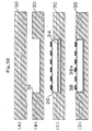
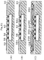
- the semiconductor device is mounted on the sheet at the bottom of the through hole of the core substrate so that the terminal contacts with the sheet, the resin is filled into the through hole and then the sheet is peeled, thereby forming a buildup layer. That is to say, after mounting the semiconductor device on the sheet so that the terminal thereof contacts with the sheet and peeling the sheet, the buildup layer is formed on the semiconductor device. Due to this, it is possible to appropriately, electrically connect the terminal to the wiring of the buildup layer and to, therefore, manufacture a highly reliable multilayer printed circuit board into which the semiconductor device is integrated.
- a method of manufacturing a multilayer printed circuit board according to claim 36 is characterized by comprising at least the following steps (a) to (i):
- the semiconductor device is mounted on the sheet at the bottom of the through hole of the core substrate so that the terminal of the device contacts with the sheet, the resin is filled into the through hole and then the sheet is peeled, thereby forming a buildup layer. That is to say, after mounting the semiconductor device on the sheet so that the terminal thereof contacts with the sheet and peeling the sheet, the buildup layer is formed on the semiconductor device. Due to this, it is possible to appropriately, electrically connect the terminal to the wiring of the buildup layer and to, therefore, manufacture a highly reliable multilayer printed circuit into which the semiconductor device is integrated.
- the bottom side of the core substrate is polished to exposure the bottom of the semiconductor device, it is possible to attach a radiating plate to the bottom of the semiconductor device and to, therefore, improve the stability of the operation of the semiconductor device.
- a UV tape the viscosity of which is lowered if being applied with UV is preferable. Since the UV tape is peeled without leaving the adhesive on the terminal of the semiconductor device by applying UV, it is possible to appropriately, electrically connect the terminal to the wiring of the buildup layer and to, therefore, manufacture a highly reliable multilayer printed circuit board into which the semiconductor device is integrated.
- a taper By providing the taper, no bubbles or grooves remain between the through hole of the core substrate and the resin and the reliability of the multilayer printed circuit board can be improved. Besides, the smoothness of the core substrate can be ensured.
- a multilayer printed circuit board having interlayer insulating layers and conductor layers repeatedly formed on a substrate in which a semiconductor device is embedded, contained or stored, via holes formed in said interlayer insulating layers, and establishing electrical connection through said via holes is characterized in that:
- the region on the substrate of the multilayer printed circuit boar into which region the semiconductor device is integrated and the region on the substrate into which the semiconductor device is not integrated are differentiated from each other. Then, the external connection terminal (BGA/PGA) is provided in the region of the substrate into which region the semiconductor device is not integrated.
- Peeling or cracking which occurs to the surrounding of the above-stated external connection terminal is resulted from the difference in thermal expansion among the semiconductor device, the external substrate, the interlayer insulating layer and the solder resist layer. That is to say, the semiconductor device and the external substrate made of ceramic are high in the coefficient of thermal expansion and expanded less by thermal expansion.
- the interlayer insulating layer and the solder resist layer made of the resin are higher in the coefficient of thermal expansion than the semiconductor device and the external substrate and, therefore, expanded more by the thermal expansion. Because of this difference in the coefficient of thermal expansion, a stress is concentrated on the surrounding of the external connection terminal (GBA/PGA) or the like and peeling and cracking occur.
- the external connection terminal (BGA/PGA) in the region on the substrate into which region the semiconductor device is not integrated, the influence of thermal expansion can be reduced. Therefore, it is possible to prevent peeling and cracking from occurring to the surrounding of the external connection terminal (BGA/PGA) or the like. Accordingly, it is possible to prevent the detachment and positional error of the external connection terminal (BGA/PGA) and to improve electrical connection characteristics and reliability.
- the external connection terminal signifies a terminal for connecting a substrate, on which an IC chip is mounted, to an external substrate or so-called mother board or daughter board.
- the terminal described herein refers to a BGA, PGA or a solder bump.
- the invention recited in claim 42 according to the multilayer printed circuit board recited in claim 41 is technically characterized by forming the transition layer on the pad portion of the semiconductor device so as to be connected to the via hole formed in the lowermost interlayer resin insulating layer.
- the transition layer is formed to cover the pad of the semiconductor device.
- a solvent can be used and a resin residue on the die pad can be prevented.
- the die pad is not discolored or dissolved.
- the formation of the oxide film of the die pad is prevented.
- the transition layer has a diameter equal to or larger than the diameter of the via hole.
- a multilayer printed circuit board according to claim 41 is characterized in that:
- the adhesion between the substrate and the semiconductor device can be improved.
- this resin filling material can prevent the cracking of the core substrate and the waviness of the interlayer resin insulating layer and the solder resist layer. Due to this, it is possible to prevent peeling and cracking from occurring to the surrounding of the solder bump or the like. Accordingly, it is possible to prevent the detachment and positional error of the solder bump and to, therefore, improve electrical connection characteristics and reliability.
- the resin filling material a thermosetting resin, a thermoplastic resin or a mixture thereof can be used as the resin filling material.
- FIG. 3(A) is a cross-sectional view of a semiconductor device 20
- FIG. 4(B) is a plan view thereof.
- transition layers 38 mainly comprising copper are formed on the respective die pads 22.
- Each transition layer 38 comprises a thin film layer 33 and a thickening layer 37. In other words, the transition layer 38 is formed out of metallic films of two or more layers.
- the thin film layer 33 is formed out of chromium.
- the thin film layer 33 is formed out of titanium. Titanium is provided by deposition or sputtering. Since titanium has good adhesiveness to metal, it is possible to suppress the entry of moisture.
- the thin film layer 33 is formed out of chromium.
- a thin film layer 33 is formed out of tin. Since tin has good adhesiveness to metal, it is possible to suppress the entry of moisture.
- a thin film layer 33 is formed out of chromium.
- the thin film layer 33 is formed out of zinc.
- a thin film layer 33 is formed out of chromium.
- the thin film layer 33 is formed out of nickel.
- Nickel is provided by sputtering. Since nickel has good adhesiveness to metal, it is possible to suppress the entry of moisture.
- a thin film layer 33 is formed out of chromium.
- the thin film layer 33 is formed out of cobalt.
- copper may be further built up on the thin film layer.
- each of the transition layers 38 has a two-layer structure comprising the thin film layer 33 and the thickening layer 37.
- each transition layer 38 is constituted to have a three-layer structure comprising the first thin film layer 33, the second thin film layer 36 and a thickening layer 37 as shown in FIG. 7(B).
- the first thin layer 33 is formed out of chromium
- the second thin film layer 36 is formed by electroless copper plating
- the thickening layer 37 is formed by copper electroplating.
- the first thin film layer 33 is formed out of chromium
- the second thin film layer 36 is formed by sputtering copper
- the thickening layer 37 is formed by copper electroplating.
- the thickness of the chromium layer is 0.07 ⁇ m, that of the copper layer is 0.5 ⁇ m and that of the electroplated copper layer is 15 ⁇ m.
- the first thin film layer 33 is formed out of titanium
- the second thin film layer 36 is formed by electroless copper plating
- the thickening layer 37 is formed by copper electroplating.
- the thickness of the titanium layer is 0.07 ⁇ m, that of the copper plated layer is 1.0 ⁇ m and that of the copper electroplated layer is 17 ⁇ m.
- the first thin film layer 33 is formed out of titanium
- the second thin film layer 36 is formed by sputtering copper
- the thickening layer 37 is formed by copper electroplating.
- the thickness of the titanium layer is 0.06 ⁇ m, that of the copper layer is 0.5 ⁇ m and that of the copper electroplated layer is 15 ⁇ m.
- the first thin film layer 33 is formed out of chromium
- the second thin film layer 36 is formed by electroless nickel plating
- the thickening layer 37 is formed by copper electroplating.
- the thickness of the chromium layer is 0.07 ⁇ m, that of the copper plated layer is 1.0 ⁇ m and the copper electroplated layer is 15 ⁇ m.
- the thin film layer 33 is formed out of titanium
- the second thin film layer 36 is formed by electroless nickel plating
- the thickening layer 37 is formed by copper electroplating.
- the thickness of the titanium layer is 0.05 ⁇ m, that of the nickel plated layer is 1.2 ⁇ m and that of the copper electroplated layer is 15 ⁇ m.
- the method of manufacturing a semiconductor device 20 according to the second modification will be described with reference to FIG. 8.
- the constitution of the semiconductor device in the second modification is almost the same as that in the first embodiment stated above with reference to FIG. 3(B).
- a semi-additive step is employed and the thickening layers 37 are formed on the respective resist unformed portions, thereby forming the transition layers 38.
- an additive step is employed and thickening layers 37 are uniformly formed. Thereafter, a resist is provided and resist unformed portions are etched away, thereby forming transition layers 38.
- the thin film layer 33 is formed out of chromium.
- a thin film layer 33 is formed out of titanium.
- each transition layer 38 has a two-layer structure comprising the thin film layer 33 and the thickening layer 37.
- a transition layer 38 is constituted to have a three-layer structure comprising the first thin film layer 33, the second thin film layer 36 and a thickening layer 37.
- the first thin film layer 33 is formed out of chromium
- the second thin film layer 36 is formed by electroless copper plating
- the thickening layer 37 is formed by copper electroplating.
- the first thin film layer 33 is formed out of chromium
- the second thin film layer 36 is formed by sputtering copper
- a thickening layer 37 is formed by-copper electroplating.
- the thickness of the chromium layer is 0.07 ⁇ m, that of the copper layer is 0.5 ⁇ m and that of the copper electroplated layer is 15 ⁇ m.
- the first thin film layer 33 is formed out of titanium
- the second thin film layer 36 is formed by electroless copper plating
- a thickening layer 37 is formed by copper electroplating.
- the thickness of the titanium layer is 0.07 ⁇ m, that of the copper layer is 1.0 ⁇ m and that of the copper electroplated layer is 15 ⁇ m.
- the first thin film layer 33 is formed out of titanium
- the second thin film layer 36 is formed by sputtering copper
- the thickening layer 37 is formed by copper electroplating.
- the thickness of the titanium layer is 0.07 ⁇ m, that of the copper layer is 0.5 ⁇ m and that of the copper electroplated layer is 18 ⁇ m.
- the first thin film layer 33 is formed out of chromium
- the second thin film layer 36 is formed by electroless nickel plating
- a thickening layer 37 is formed by copper electroplating.
- the thickness of the chromium layer is 0.06 ⁇ m
- that of the nickel layer is 1.2 ⁇ m
- that of the copper electroplated layer is 16 ⁇ m.
- the first thin film layer 33 is formed out of titanium
- the second thin film layer 36 is formed by electroless nickel plating
- a thickening layer 37 is formed by copper electroplating.
- the thickness of the titanium layer is 0.07 ⁇ m
- that of the nickel layer is 1.1 ⁇ m
- that of the copper electroplated layer is 15 ⁇ m.
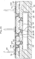
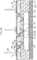
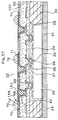
- the multilayer printed circuit board 10 comprises a core substrate 30 containing therein an IC chip 20, an interlayer resin insulating layer 50 and an interlayer resin insulating layer 150. Via holes 60 and conductor circuits 58 are formed on the interlayer resin insulating layer 50. Via holes 160 and conductor circuits 158 are formed on the interlayer resin insulating layer 150.
- solder resist layer 70 is provided on the interlayer resin insulating layer 150.
- Solder bumps 76 for connecting to an external substrate such as a daughter board or a mother board, which is not shown in FIG. 14, are provided on the conductor circuits 158 under the openings 71 of the solder resist layer 70, respectively.
- the IC chip 20 is integrated into the core substrate 30 and transition layers 38 are provided on the respective pads 22 of the IC chip 20. Due to this, it is possible to electrically connect the IC chip to the multilayer printed circuit board (or package substrate) without using lead members and a sealing resin. Further, since the transition layers 38 are formed on the IC chip portion, the IC chip portion is flattened and the upper interlayer insulating layer 50 is, therefore, flattened to thereby provide uniform film thickness. Further, because of the transition layers, it is possible to maintain the stability of shape even if the via holes 60 provided in the upper layer are formed.
- transition layers 38 made of copper on the respective die pads 22, it is possible to prevent resin residues on the die pads 22 and to prevent the die pads 22 from being discolored or dissolved even after impregnating the multilayer printed circuit board in an acid, an oxidizer or an etching solution in a later step or conducting various annealing steps.
- connection characteristic between the die pads of the IC chip and the via holes and reliability can be improved.
- interposing the transition layers 38 each having a diameter of 60 ⁇ m or more on the respective pads 22 each having a diameter of 40 ⁇ m it is possible to ensure connecting the via holes each having a diameter of 60 ⁇ m.
- an Ni/Cu alloy 52 can be formed on the surface of the interlayer epoxy resin insulating layer 50 by conducting sputtering with an Ni-Cu alloy 52 as a target under conditions of an air pressure of 0.6 Pa, a temperature of 80° C, power of 200W and a duration of five minutes using SV-4540 manufactured by ULVAC JAPAN LTD. At this moment, the thickness of the Ni-Cu alloy layer 52 thus formed is 0.2 ⁇ m.
- solder paste Sn/Pb, Sn/Sb, Sn/Ag, Sn/Ag/Cu or the like may be used. Needless to say, a solder paste of low a radiation ray type may be used.
- thermosetting resin sheet is used for the interlayer resin insulating layers 50 and 150.
- the thermosetting resin insulating sheet contains a refractory resin, soluble particles, a hardening agent and other components. The materials will now be described one by one.
- the resin used in the manufacturing method of the present invention has a structure in that particles soluble in acid or an oxidizer (hereinafter, referred to as “soluble particles”) are dispersed in resin which is refractory with respect to acid or an oxidizer (hereinafter, referred to as “refractory resin”).
- the soluble particles are exemplified by resin particles which are soluble in acid or an oxidizer (hereinafter called “soluble resin particles”), inorganic particles which are soluble in acid or an oxidizer (hereinafter called “inorganic soluble particles”) and metal particles which are soluble in acid or an oxidizer (hereinafter called “soluble metal particles”).
- soluble resin particles resin particles which are soluble in acid or an oxidizer
- inorganic soluble particles inorganic particles which are soluble in acid or an oxidizer
- metal particles which are soluble in acid or an oxidizer
- each of the soluble particles is not limited.
- the shape may be a spherical shape or a pulverized shape. It is preferable that the particles have a uniform shape. The reason for this lies in that a rough surface having uniformly rough pits and projections can be formed.
- the mean particle size of the soluble particles is 0.1 ⁇ m to 10 ⁇ m.
- particles having two or more particle sizes may be employed. That is, soluble particles having a mean particle size of 0.1 ⁇ m to 0.5 ⁇ m and soluble particles having a mean particle size of 1 ⁇ m to 3 ⁇ mm may be mixed. Thus, a more complicated rough surface can be formed. Moreover, the adhesiveness with the conductor circuit can be improved.
- the particle size of the soluble particles is the length of a longest portion of each of the soluble particles.
- the soluble resin particles may be particles constituted by thermosetting resin or thermoplastic resin. When the particles are immersed in solution composed of acid or an oxidizer, the particles must exhibit dissolving rate higher than that of the foregoing refractory resin.
- the soluble resin particles are exemplified by particles constituted by epoxy resin, phenol resin, polyimide resin, polyphenylene resin, polyolefin resin polietelslufon or fluorine resin.
- the foregoing material may be employed solely or two or more materials may be mixed.
- the soluble resin particles may be resin particles constituted by rubber.
- Rubber above is exemplified by polybutadiene rubber, a variety of denatured polybutadiene rubber, such as denatured epoxy rubber, denatured urethane rubber or denatured (metha) acrylonitrile rubber, and (metha) acrylonitrile butadiene rubber containing a carboxylic group.
- the soluble resin particles can easily be dissolved in acid or an oxidizer. That is, when the soluble resin particles are dissolved with acid, dissolution is permitted with acid except for strong acid. When the soluble resin particles are dissolved, dissolution is permitted with permanganate which has a relatively weak oxidizing power.
- chromic acid When chromic acid is employed, dissolution is permitted even at a low concentration. Therefore, retention of the acid or the oxidizer on the surface of the resin can be prevented.
- a catalyst such as palladium chloride, is supplied after the rough surface has been formed as described later, inhibition of supply of the catalyst and oxidation of the catalyst can be prevented.
- the inorganic soluble particles are exemplified by particles made of at least a material selected from a group comprising an aluminum compound, a calcium compound, a potassium compound, a magnesium compound and a silicon compound.
- the aluminum compound is exemplified by alumina and aluminum hydroxide.
- the calcium compound is exemplified by calcium carbonate and calcium hydroxide.
- the potassium compound is exemplified by potassium carbonate.
- the magnesium compound is exemplified by magnesia, dolomite and basic magnesium carbonated.
- the silicon compound is exemplified by silica and zeolite. The foregoing material may be employed solely or two or more materials may be mixed.
- the soluble metal particles are exemplified by particles constituted by at least one material selected from a group comprising copper, nickel, iron, zinc, lead, gold, silver, aluminum, magnesium, potassium and silicon.
- the soluble metal particles may have surfaces coated with resin or the like in order to maintain an insulating characteristic.
- the combination of the two types of soluble particles is combination of resin particles and inorganic particles. Since each of the particles has low conductivity, an insulating characteristic with the resin film can be maintained. Moreover, the thermal expansion can easily be adjusted with the refractory resin. Thus, occurrence of a crack of the interlayer resin insulating layer constituted by the resin film can be prevented. Thus, separation between the interlayer resin insulating layer and the conductor circuit can be prevented.
- the refractory resin is not limited when the resin is able to maintain the shape of the rough surface when the rough surface is formed on the interlayer resin insulating layer by using acid or oxidizer.
- the refractory resin is exemplified by thermosetting resin, thermoplastic resin and their composite material.
- the foregoing photosensitive resin of a type having photosensitive characteristic imparted thereto may be employed. When the photosensitive resin is employed, exposure and development processes of the interlayer resin insulating layers can be performed to form the openings for the via holes.
- the resin containing thermosetting resin is employed.
- the shape of the rough surface can be maintained against plating solution and when a variety of heating processes are performed.
- the refractory resin is exemplified by epoxy resin, phenol resin, phenoxy resin, polyimide resin, polyphenylene resin, polyolefin resin, polyetelslufon and fluorine resin.
- the foregoing material may be employed solely or two or more types of the materials may be mixed.
- epoxy resin having two or more epoxy groups in one molecule thereof is employed.
- the reason for this lies in that the foregoing rough surface can be formed. Moreover, excellent heat resistance and the like can be obtained. Thus, concentration of stress onto the metal layer can be prevented even under a heat cycle condition. Thus, occurrence of separation of the metal layer can be prevented.
- the epoxy resin is exemplified by cresol novolac epoxy resin, bisphenol-A epoxy resin, bisphenol-F epoxy resin, phenol novolac epoxy resin, alkylphenol novolac epoxy resin, biphenol-F epoxy resin, naphthalene epoxy resin, dicyclopentadiene epoxy resin, an epoxy material constituted by a condensation material of phenol and an aromatic aldehyde having a phenol hydroxyl group, triglycidyl isocyanurate and alicyclic epoxy resin.
- the foregoing material may be employed solely or two or more material may be mixed. Thus, excellent heat resistance can be realized.
- the soluble particles in the resin film according to the present invention are substantially uniformly dispersed in the refractory resin.
- the reason for this lies in that a rough surface having uniform pits and projections can be formed.
- a resin film containing soluble particles in only the surface on which the rough surface is formed may be employed.
- the portions of the resin film except for the surface is not exposed to acid or the oxidizer. Therefore, the insulating characteristic between conductor circuits through the interlayer resin insulating layer can reliably be maintained.
- the amount of the soluble particles which are dispersed in the refractory resin is 3 wt% to 40 wt% with respect to the resin film.
- the amount of mixture of the soluble particles is lower than 3 wt%, the rough surface having required pits and projections cannot be formed.
- the amount is higher than 40 wt%, deep portions of the resin film are undesirably dissolved when the soluble particles are dissolved by using acid or the oxidizer.
- the insulating characteristic between the conductor circuits through the interlayer resin insulating layer constituted by the resin film cannot be maintained. Thus, short circuit is sometimes is caused to occur.
- the resin film contains a hardening agent and other components as well as the refractory resin.
- the hardening agent is exemplified by an imidazole hardening agent, an amine hardening agent, a guanidine hardening agent, an epoxy adduct of each of the foregoing hardening agents, a microcapsule of each of the foregoing hardening agents and an organic phosphine compound, such as triphenylphosphine or tetraphenyl phosphonium tetraphenyl borate.
- the content of the hardening agent is 0.05 wt% to 10 wt% with respect to the resin film.
- the content is lower than 0.05 wt%.
- the resin film cannot sufficiently be hardened.
- introduction of acid and the oxidizer into the resin film occurs greatly.
- the insulating characteristic of the resin film sometimes deteriorates.
- an excessively large quantity of the hardening agent component sometimes denatures the composition of the resin.
- the reliability sometimes deteriorates.
- the other components are exemplified by an inorganic compound which does not exert an influence on the formation of the rough surface and a filler constituted by resin.
- the inorganic compound is exemplified by silica, alumina and dolomite.
- the resin is exemplified by polyimide resin, polyacrylic resin, polyamideimide resin, polyphenylene resin, melanine resin and olefin resin.
- the resin film may contain solvent.
- the solvent is exemplified by ketone, such as acetone, methylethylketone or cyclohexane; aromatic hydrocarbon, such as ethyl acetate, butyl acetate, cellosolve acetate, toluene or xylene.
- ketone such as acetone, methylethylketone or cyclohexane
- aromatic hydrocarbon such as ethyl acetate, butyl acetate, cellosolve acetate, toluene or xylene.
- the foregoing material may be employed solely or two or more materials may be mixed. It is noted, however, interlayer resin insulating layer is resolved and carbonated if heated at a temperature of 350° C or higher.
- a semiconductor device is the same as that in the first embodiment. However, in the comparison example 1, no transition layers are formed and die pads are directly embedded into a multilayer printed circuit board.
- the IC chip and the printed circuit board can be connected to each other without using lead members. Due to this, resin sealing becomes unnecessary. Furthermore, since no defects resulting from the lead members and sealing resin occur, connection characteristic and reliability are improved. Besides, since the pads of the IC chip are directly connected to the conductive layers of the printed circuit board, it is possible to improve electrical characteristic.
- the wiring length from the IC chip to the substrate to the external substrate can be advantageously shortened and loop inductance can be advantageously reduced.
- the degree of freedom for wiring formation increases to the extent that BGA's and PGA's can be provided.
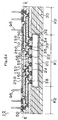
- the multilayer printed circuit board 10 comprises a heat sink 30D on which the IC chip 20 in the first embodiment stated above with reference to FIG. 3(B) is mounted, a core substrate 31 containing therein the IC chip 20, an interlayer resin insulating layer 50 and an interlayer resin insulating layer 150. Via holes 60 and conductor circuits 58 are formed on the interlayer resin insulating layer 50. Via holes 160 and conductor circuits 158 are formed on the interlayer resin insulating layer 150.
- solder resist layer 70 is provided on the interlayer resin insulating layer 150.
- the heat sink 30D is made of ceramic such as aluminum nitride, alumina or mullite, or metal such as aluminum alloy, copper or phosphor bronze.
- the aluminum alloy having heat conductivity or a copper foil both sides of which have been subjected to a roughening process is appropriate.
- the heat sink 30D is attached to the rear surface of the IC chip 20 embedded into the core substrate 31, thereby emitting heat generated in the IC chip 20, preventing the core substrate 31 and the interlayer resin insulating layers 50 and 150 formed on the core substrate 31 from warping and preventing the breakage of the via holes 60, 160 and the conductor circuits 58 and 158 on the interlayer resin insulating layers.
- the reliability of wirings enhances.
- the IC chip 20 is integrated into the core substrate 31 and transition layers 38 are provided on the respective pads 22 of the IC chip 20. Due to this, it is possible to electrically connect the IC chip to the multilayer printed circuit board (or package substrate) without using leadmembers and a sealing resin. Further, since the transition layers 38 are formed on the IC chip portion, the IC chip portion is flattened and the upper interlayer insulating layer 50 is, therefore, flattened to thereby provide uniform film thickness. Further, because of the transition layers, it is possible to maintain the stability of shape even if the via holes 60 provided in the upper layer are formed.
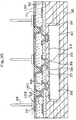
- the multilayer printed circuit board is constituted in a PGA type for establishing connection through conductive connection pins 96 as shown in FIG. 26. Also, via holes are formed by laser in the above-stated second embodiment, whereas via holes are formed by phptoetching in the first modification.
- the heat sink is attached to the rear surfaces of the IC chips embedded in the core substrate, thereby allow heat generated in the IC chip to be discharged. By doing so, it is possible to prevent the core substrate and interlayer resin insulating layers formed on the core substrate from warping, and prevent the breakage of the via holes and the conductor circuits on the interlayer resin insulating layers.
- the wiring length from the IC chip to the substrate to the external substrate can be advantageously shortened and loop inductance can be advantageously reduced.
- a multilayer printed circuit board 10 in the third embodiment comprises a core substrate 30 containing therein an IC chip 20, an interlayer resin insulating layer 50 and an interlayer resin insulating layer 150. Via holes 60 and conductor circuits 58 are formed on the interlayer resin insulating layer 50. Via holes 160 and conductor circuits 158 are formed on the interlayer resin insulating layer 150.
- the IC chip 20 is integrated into a core substrate 30 and transition layers 38 are provided on the respective pads 22 of the IC chip 20. Due to this, it is possible to connect the IC chip to the multilayer printed circuit board (or package substrate) without using lead members and a sealing resin. Also, since the transition layers 38 are formed on the IC chip portion, the IC chip portion is flattened and the upper interlayer resin insulating layer 50 is flattened accordingly, thereby providing uniform film thickness. Further, the transition layers allow maintaining shape even if the upper via holes 60 are formed.
- transition layers 38 made of copper on the respective die pads 22, it is possible to prevent resin residues on the die pads 22 and to prevent the die pads 22 from being discolored or dissolved even after impregnating the multilayer printed circuit board in an acid, an oxidizer or an etching solution in a later step or conducting various annealing steps.
- connection characteristic between the die pads of the IC chip and the via holes and reliability can be improved.
- interposing the transition layers 38 each having a diameter of 60 ⁇ m or more on the respective pads 22 each having a diameter of 40 ⁇ m it is possible to ensure connecting the via holes each having a diameter of 60 ⁇ m.
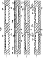
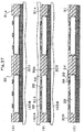
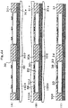
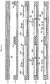
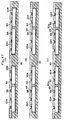
- a multilayer printed circuit board into which semiconductor devices are integrated is manufactured for obtaining multiple multilayer printed circuit boards. Then, as shown in FIG. 32(C), the multilayer printed circuit board is cut into pieces, thereby obtaining a plurality of multilayer printed circuit boards. Due to this, it is possible to efficiently manufacture highly reliable multilayer printed circuit boards 10 (see FIG. 33).
- a multilayer printed circuit board according to the other example of the third embodiment will be described with reference to FIG. 35.
- the multilayer printed circuit board is constituted in a PGA type for establishing connection through conductive connection pins 96 as shown in FIG. 35. Also, via holes are formed by laser in the above-stated third embodiment, whereas via holes are formed by phptoetching in the first another example.
- the IC chip is embedded into the core substrate.
- a heat sink 30D is attached to the rear surface of an IC chip 20.
- the multilayer printed circuit board 10 comprises the heat sink 30D, a core substrate 31 containing therein the IC chip 20, an interlayer resin insulating layer 50 and an interlayer resin insulating layer 150 above the IC chip 20.
- Via holes 60 and conductor circuits 58 are formed on the interlayer resin insulating layer 50.
- Via holes 160 and conductor circuits 158 are formed on the interlayer resin insulating layer 150.
- solder resist layer 70 is provided on the interlayer resin insulating layer 150.
- the heat sink 30D is made of ceramic such as aluminum nitride, alumina or mullite, or metal such as aluminum alloy, copper or phosphor bronze.
- the aluminum alloy having heat conductivity or a copper foil both sides of which have been subjected to a roughening process is appropriate.
- the heat sink 30D is attached to the rear surface of the IC chip 20 embedded into the core substrate 31, thereby emitting heat generated in the IC chip 20, preventing the core substrate 31 and the interlayer resin insulating layers 50 and 150 formed on the core substrate 31 from warping and preventing the breakage of the via holes 60, 160 and the conductor circuits 58 and 158 on the interlayer resin insulating layers.
- the reliability of wirings enhances.
- the IC chip 20 is attached to the heat sink 30D by conductive adhesive 29.
- the conductive adhesive 29 has resin containing metallic powder such as copper, silver, gold or aluminum and has high heat conductivity, so that the heat generated in the IC chip 20 can be efficiently emitted toward the heat sink 30D.
- the conductive adhesive is used to attach the IC chip 20 to the heat sink 30D; however, various adhesives are available as long as they have high heat conductivity.
- the IC chip 20 is integrated into the core substrate 30 and transition layers 38 are provided on the respective pads 22 of the IC chip 20. Due to this, it is possible to electrically connect the IC chip to the multilayer printed circuit board (or package substrate) without using lead members and a sealing resin. Further, since the transition layers 38 are formed on the IC chip portion, the IC chip portion is flattened and the upper interlayer insulating layer 50 is, therefore, flattened to thereby provide uniform film thickness . Further, because of the transition layers, it is possible to maintain the stability of shape even if the via holes 60 provided in the upper layer are formed.
- transition layers 38 made of copper on the respective die pads 22, it is possible to prevent resin residues on the die pads 22 and to prevent the die pads 22 from being discolored or dissolved even after impregnating the multilayer printed circuit board in an acid, an oxidizer or an etching solution in a later step or conducting various annealing steps.
- connection characteristic between the die pads of the IC chip and the via holes and reliability can be improved.
- interposing the transition layers 38 each having a diameter of 60 ⁇ m or more on the respective pads 22 each having a diameter of 40 ⁇ m it is possible to ensure connecting the via holes each having a diameter of 60 ⁇ m.
- the multilayer printed circuit board is constituted in a PGA type for establishing connection through conductive connection pins 96 as shown in FIG. 43. Also, via holes are formed by laser in the above-stated first embodiment, whereas via holes are formed by phptoetching in the first another example.
- the core substrate 30 is formed out of prepregs.
- a resin substrate obtained by curing prepregs is fixed to a heat sink 30D by prepregs.
- FIG. 50 shows the cross section of a multilayer printed circuit board 10.
- the multilayer printed circuit board 10 contains an IC chip (or CPU) 20A and an IC chip (or a cache memory) 20B in a core substrate 30.
- IC chip or CPU
- IC chip or a cache memory
- interlayer resin insulating layers 50 and 150 are formed on the core substrate 30.
- Via holes 60 and conductor circuits 58 are formed on the interlayer resin insulating layer 50.
- Via holes 160 and conductor circuits 158 are formed on the interlayer resin insulating layer 150.
- the IC chips 20A and 20B are covered with a passivation film 24 and die pads 22 constituting input/output terminals are provided in the openings of the passivation film 24.
- Transition layers 38 are formed on the respective die pads 22 made of aluminum. Each transition layer 38 has a three-layer structure comprising the first thin film layer 33, the second thin film layer 36 and a thickening layer 37.
- solder resist layer 70 is provided on the interlayer resin insulating layer 150.
- the IC chips 20A and 20B are integrated into a core substrate 30 in advance and the transition layers 38 are provided on the respective pads 22 of the IC chips 20A and 20B. Due to this, it is possible to electrically connect the IC chips to the multilayer printed circuit board (or package substrate) without using lead members and a sealing resin. Further, since the transition layers 38 are formed on the IC chip portions, the IC chip portions are flattened and an interlayer insulating layer 50 provided above the chips is, therefore, flattened to thereby provide uniform film thickness. Further, because of the transition layers, it is possible to maintain the stability of shape even if via holes 60 provided in the upper layer are formed.
- transition layers 38 made of copper on the respective die pads 22, it is possible to prevent resin residues on the die pads 22 and to prevent the die pads 22 from being discolored or dissolved even after impregnating the multilayer printed circuit board in an acid, an oxidizer or an etching solution in a later step or conducting various annealing steps.
- connection characteristic between the die pads of the IC chips and the via holes and reliability can be improved.
- interposing the transition layers 38 each having a diameter of 60 ⁇ m or more on the respective pads 22 each having a diameter of 40 ⁇ m it is possible to ensure connecting the via holes each having a diameter of 60 ⁇ m.
- the IC chip 20A for a CPU and the IC chip 20B for a cache memory are separately embedded into the printed circuit board. Since the IC chips can be more economical if they are formed separately and the chips are located adjacent, to each other, transmission delay or malfunction does not occur. Besides, even if the design of the printed circuit board is changed, there is no need to change the design of the IC chips themselves and the degree of freedom for formation can be increased.
- An adhesive layer 34 is filled into the recess 32 of the printed circuit board in the second modification of the third embodiment.
- the adhesive 34 can suppress the behaviors of the IC chips 20A and 20B and maintain smoothness even after a heat history during a heat cycle and via hole formation. Due to this, the connection portions between the IC chips and the via holes are not peeled or broken or the interlayer insulating layers 50 and 150 do not crack. It is also possible to improve reliability.
- the transition layers 38 are formed on the IC chip and then the IC chip is contained in the core substrate.
- the IC chips are contained in the core substrate and then the transition layers 38 are formed.
- FIG. 52 shows the printed circuit board according to the first other example.
- the printed circuit board according to the first other example is the same as the printed circuit board according to the second modification stated above with reference to FIG. 50.
- the IC chips are contained in the core substrate 30 and then the transition layers 38 are formed.
- transition layers 38 are formed on IC chips and then the IC chips are contained in a core substrate as in the case of the first embodiment.
- transition layers 38 are provided on the IC chips 20A and 20B in the same manner as the manufacturing method of the first embodiment discribed above.
- the transition layers on the die pads by providing the transition layers on the die pads, it is possible to prevent resin residues on the pads and the connection characteristics between the die pads and the via holes and reliability can be improved. Further, multiple multilayer printed circuit boards provided with semiconductor devices are manufactured. Then, the substrate is cut into pieces and a plurality of multilayer printed circuit boards are obtained. Due to this, it is possible to efficiently manufacture highly reliable multilayer printed circuit boards .
- the wiring length from the IC chip to the substrate to the external substrate can be advantageously shortened and loop inductance can be advantageously reduced.
- a multilayer printed circuit board in the fourth embodiment comprises a core substrate 30 containing therein an IC chip 20, an interlayer resin insulating layer 50 and an interlayer resin insulating layer 150. Via holes 60 and conductor circuits 58 are formed on the interlayer resin insulating layer 50. Via holes 160 and conductor circuits 158 are formed on the interlayer resin insulating layer 150.
- a radiating plate 44 is attached to the rear surface of the IC chip 20.
- solder resist layer 70 is provided on the interlayer resin insulating layer 150.
- Solder bumps 76 for connecting to an external substrate, which is not shown, such as a daughter board or a mother board are provided on the conductor circuit 158 under the opening portions 71 of the solder resist layer 70.
- die pads 22 and wirings are provided on the upper surface of the IC chip 20
- a passivation film 24 is covered on the die pads 22 and the wirings and the openings of the passivation film 24 are formed in the respective die pads 22.
- Transition layers 38 mainly comprising copper are formed on the respective die pads 22.
- Each transition layer 38 comprises a thin film layer 33 and an electroplated film 37.
- the IC chip 20 is integrated into a core substrate 30 and the transition layers 38 are provided on the respective pads 22 of the IC chip 20. Due to this, it is possible to connect the IC chip to the multilayer printed circuit board (or package substrate) electricaly without using lead members and a sealing resin. Also, since the transition layers 38 are formed on the IC chip portion, the IC chip portion is flattened and the upper interlayer resin insulating layer 50 is flattened accordingly, thereby providing uniform film thickness. Further, the transition layers allow maintaining shape even if the upper via holes 60 are formed.
- transition layers 38 made of copper on the respective die pads 22, it is possible to prevent resin residues on the die pads 22 and to prevent the die pads 22 from being discolored or dissolved even after impregnating the multilayer printed circuit board in an acid, an oxidizer or an etching solution in a later step or conducting various annealing steps.
- connection characteristic between the die pads of the IC chip and the via holes and reliability can be improved.
- interposing the transition layers 38 each having a diameter of 60 ⁇ m or more on the respective pads 22 each having a diameter of 40 ⁇ m it is possible to ensure connecting the via holes each having a diameter of 60 ⁇ m.
- the IC chip 20 is mounted so that the die pads 38 contact with the UV tape 40, the UV tape 40 is peeled and then the buildup layers are formed on the IC chip 20. Due to this, it is possible to appropriately, electrically connect the IC chip to the via holes 60 of the buildup layers-and to manufacture a highly reliable multilayer printed circuit board into which a semiconductor device is integrated.
- the semiconductor device is mounted on the sheet at the bottom of the through hole of the core substrate so that terminals contact with the sheet, the sheet is peeled after the resin is filled into the through hole and the buildup layers are formed.
- the semiconductor device is mounted on the sheet so that the terminals contact with the sheet and the buildup layers are formed on the semiconductor device after peeling the sheet.
- FIG. 63 shows the cross section of a multilayer printed circuit board 10.
- the multilayer printed circuit board 10 comprises a core substrate 30 containing therein an IC chip 20, an interlayer resin insulating layer 50, an interlayer resin insulating layer 150 and an interlayer resin insulating layer 250.
- Via holes 60 and conductor circuits 58 are formed on the interlayer resin insulating layer 50.
- Via holes 160 and conductor circuits 158 are formed on the interlayer resin insulating layer 150.
- Via holes 260 and conductor circuits 258 are formed on the interlayer resin insulating layer 250.
- a solder resist layer 70 is provided on the interlayer resin insulating layer 250.
- the BGA's 76 are provided in a region R2 other than a region R1 right above the IC chip 20.
- the IC chip 20 is covered with a passivation film 24 protecting the IC chip 20 and die pads 22 each constituting an input/output terminal are provided in the respective openings of the passivation film 24.
- Transition layers 38 mainly comprising copper are formed on the respective pads 22.
- An adhesive material 34 which is a resin material, is filled between the IC chip 20 and the recess 32 of the substrate 30.
- the adhesive material 34 allows the IC chip 20 to be fixed in the recess of the substrate 30. Since this resin filler material 34 relaxes a stress generated by thermal expansion, it is possible to prevent the cracking of the core substrate 30 and the waviness of the interlayer resin insulating layers 50, 150 and 250 and the solder resist layer 70. Due to this, it is possible to prevent peeling and cracking from occurring to the surroundings of the BGA's 76. It is possible to prevent the detachment and positional error of the solder bumps 76, accordingly. It is, therefore, possible to improve electrical connection characteristics and reliability.
- FIG. 65 shows the cross-sectional view of the multilayer printed circuit board 10 taken along line E-E of FIG. 63.
- An inside region denoted by a dotted line in FIG. 65 is a region R1 into which the IC chip 20 is integrated.
- a region outside of the dotted line and inside of a solid line in FIG. 65 is a region R2 into which the IC chip 20 is not integrated.
- the conductor circuits 258 are formed to radially spread from the region R1 to the region R2.
- the solder pads 75 to be connected to the BGA's 76, respectively, are arranged in the region R2 in a grid-like fashion.
- FIG. 66(A) is a plan view of the multilayer printed circuit board 10 shown in FIG. 63.
- the BGA's 76 are arranged in the region R2 in a grid-like fashion and connected to the external substrate, not shown, such as a daughter board or a mother board.
- the BGA's 76 may be formed in the region R2 in a staggered fashion as shown in FIG. 66(B).
- the BGA's 76 are provided in the region R2 on the substrate into which region the IC chip is not integrated.
- the BGA's 76 in the region R2 other than the region right above the IC chip 20, it is possible to reduce the influence of the thermal expansion of the IC chip 20 made of ceramic and having a low coefficient of thermal expansion and the interlayer insulating layers 50, 150, 250 and the solder resist layer 70 each of which is made of resin and has a high coefficient of thermal expansion and, therefore, possible to prevent peeling and cracking from occurring to the surroundings of the BGA's 76 and the like. Accordingly, it is possible to prevent the detachment and positional error of the solder bumps 76 and to improve electrical connection characteristics and reliability.
- the IC chip 20 is integrated into the core substrate 30 and the transition layers 38 are provided on the respective pads 22 of the IC chip 20. Due to this, it is possible to electrically connect the IC chip to the multilayer printed circuit board (or package substrate) without using lead members and a sealing resin. Further, since the transition layers 38 are formed on the IC chip portion, the IC chip portion is flattened and the upper interlayer insulating layer 50 is, therefore, flattened to thereby provide uniform film thickness. Further, because of the transition layers, it is possible to maintain the stability of shape even if the via holes 60 provided in the upper layer are formed.
- transition layers 38 made of copper on the respective die pads 22, it is possible to prevent resin residues on the die pads 22 and to prevent the die pads 22 from being discolored or dissolved even after impregnating the multilayer printed circuit board in an acid, an oxidizer or an etching solution in a later step or conducting various annealing steps.
- connection characteristic between the die pads of the IC chip and the via holes and reliability can be improved.
- interposing the transition layers 38 each having a diameter of 60 ⁇ m or more on the respective pads 22 each having a diameter of 40 ⁇ m it is possible to ensure connecting the via holes each having a diameter of 60 ⁇ m.
- the transition layers 38 are formed on the IC chip 20 and then the IC chip 20 is contained in the core substrate 30.
- an IC chip is contained in a core substrate and then transition layers are formed.
- a multilayer printed circuit board according to comparison example 3 will be described.
- the BGA's 76 are arranged in the region R2 other than the region right above the IC chip.
- BGA's 76 are uniformly arranged on a solder resist layer as shown in FIG. 66(C). Namely, the BGA's 76 are formed on the entire surface of the solder resist layer in a grid-like (or full grid-like) fashion without differentiating a region R1 from a region R2.
- the multilayer printed circuit board according to the fifth embodiment showed an appropriate result.
- cracking and/or peeling was found in the surroundings of the BGA's. Also, it was found that the contact resistance increased. The same results were obtained if PGA's instead of the BGA's as shown in FIG. 64 were used.
- the region on the substrate into which region the semiconductor device of the multilayer printed circuit board is integrated and the region on the substrate into which region the semiconductor device is not integrated are differentiated from each other.
- the external connection terminals (BGA's/PGA's) are arranged in the region on the substrate into which region the semiconductor device is not integrated. Namely, by arranging the external connection terminals (BGA's/PGA's) in the region on the substrate into which region the semiconductor device is not integrated, the influence of thermal expansion can be reduced and peeling and/or cracking can be, therefore, prevented from occurring to the surroundings of the external connection terminals (BGA's/PGA's). Accordingly, it is possible to prevent the detachment or positional error of the external connection terminals (BGA's/PGA's) and to improve electrical connection characteristics and reliability.
Landscapes
- Engineering & Computer Science (AREA)
- Microelectronics & Electronic Packaging (AREA)
- Production Of Multi-Layered Print Wiring Board (AREA)
- Manufacturing & Machinery (AREA)
- Physics & Mathematics (AREA)
- Geometry (AREA)
Abstract
A transition layer 38 is provided on a die pad 22 of an
IC chip 20 and integrated into a multilayer printed circuit board
10. Due to this, it is possible to electrically connect the
IC chip 20 to the multilayer printed circuit board 10 without
using lead members and a sealing resin. Also, by providing the
transition layer 38 made of copper on an aluminum pad 24, it
is possible to prevent a resin residue on the pad 24 and to improve
connection characteristics between the die pad 24 and a via hole
60 and reliability.
Description
The present invention relates to a semiconductor device
such as an IC chip, a semiconductor device manufacturing method,
a multilayer printed circuit board into which a semiconductor
device is integrated and a multilayer printed circuit board
manufacturing method.
An IC chip is electrically connected to a printed circuit
board by a mounting method such as wire bonding, TAB or flip
chip bonding.
In the wire bonding method, an IC chip is die-bonded to
a printed circuit board by adhesive, the pads of the printed
circuit board are connected to the pads of an IC chip by wires
such as metallic wires and then a sealing resin such as a
thermosetting resin or a thermoplastic resin is applied to
protect the IC chip and the wires.
In the TAB method, the wires referred to as leads are
connected in the block by a solder or the like and then the bumps
of an IC chip and the pads of a printed circuit board are sealed
by a resin.
In the flip chip bonding method, the pads of an IC chip
are connected to the pads of a printed circuit board through
bumps and the gaps'between the pads and the bumps are filled
with a resin.
In each of these mounting methods, however, the IC chip
is electrically connected to the printed circuit board through
connection lead members (wires, leads or bumps). The lead
members tend to be cut off and eroded, thereby breaking the
connection of the printed circuit board with the IC chip and
causing malfunctions.
Further, in each mounting method, a thermoplastic resin
such as an epoxy resin is applied to seal the IC chip so as to
protect the IC chip. If bubbles are contained at the time of
filling the resin, the breakage of lead members, the corrosion
of the IC pads and the deterioration of reliability are derived
from the bubbles. To seal members by a thermoplastic resin,
it is necessary to create resin filling plungers and metallic
molds in accordance with the respective members. In addition,
if a thermosetting resin is employed, it is necessary to select
an appropriate resin for the materials of lead members, solder
resist and the like, thereby disadvantageously causing cost
increase.
On the other hand, there has been conventionally proposed
a technique for electrically connecting an IC chip to a printed
circuit board by embedding a semiconductor device into a
substrate and forming buildup layers on the substrate instead
of attaching the IC chip to the exterior of the printed circuit
board (or package substrate) as stated above in Japanese Patent
Laid-Open Nos. 9-321408 (or USP5875100), 10-256429, 11-126978
and the like.
According to Japanese Patent Laid-Open No. 9-321408 (or
USP5875100), a semiconductor device having stud bumps formed
on die pads is embedded into a printed circuit board and wirings
are formed on the stud bumps to thereby electrically connect
the printed circuit board to the semiconductor device. However,
since the stud bumps are onion-shaped and irregular in height,
smoothness is deteriorated if an interlayer insulating layer
is formed and electrical connection cannot be established even
if via holes are formed. Further, since the stud bumps are
provided by bonding one by one, they cannot be provided
collectively and productivity is thereby disadvantageously
lowered.
Japanese Patent Laid-Open No. 10-256429 shows a structure
in which a semiconductor device is contained in a ceramic
substrate and the substrate is electrically connected to the
semiconductor device by flip chip bonding. However, ceramic
is inferior in outline workability and the semiconductor device
cannot be appropriately contained in the ceramic substrate.
Besides, the bumps are irregular in height. Due to this, the
smoothness of an interlayer insulating layer is deteriorated
and connection characteristic is deteriorated accordingly.
Japanese Patent Laid-Open No.11-126978 shows amultilayer
printed circuit board wherein an electrical component such as
a semiconductor device is embedded into a gap or containing
portion, connected to a conductor circuit and built up through
via holes. However, since the containing portion is a gap, a
positional error tends to occur and the substrate cannot be often
connected to the pads of the semiconductor device. Besides,
since die pads are directly connected to the conductor circuit,
oxide coats tend to be formed on the respective die pads, thereby
disadvantageously increasing insulating resistance.
The present invention has been made to improve the
above-stated problems. It is an object of the present invention
to provide a semiconductor device manufacturing method which
allows a semiconductor device to be directly electrical connected
to a printed circuit board without using lead members.
Meanwhile, if a semiconductor device is embedded into a
printed circuit board made of resin, then the printed circuit
board is warped by heat generated in the semiconductor device,
internal wirings are cut off and reliability is thereby
disadvantageously deteriorated.
The present invention has been made to improve the
above-stated problem. It is, therefore, a still further object
of the present invention to provide a multilayer printed circuit
board into which a semiconductor device is integrated and the
method of manufacturing the multilayer printed circuit board.
Furthermore, conventionally, a highly reliable printed
circuit board into which a semiconductor device is integrated
cannot be efficiently manufactured.
The present invention has been made to improve the above
problem. It is, therefore, a still further object of the present
invention to provide a manufacturing method capable of
efficiently manufacturing a highly reliable multilayer printed
circuit board into which a semiconductor device is integrated.
Moreover, if a multilayer printed circuit board comprising
a substrate into which a semiconductor device is embedded and
contained, is employed as a package substrate, a chip set or
the like, the multilayer printed circuit board can fulfill its
behaviors by being electrically connected to an external
substrate (which is a so-called mother board or a daughter board).
Due to this, it is necessary to provide BGA's and conductive
connection pins (PGA's) on the multilayer printed circuit board.
The BGA's and PGA's are formed by providing solder pads on a
solder resist layer on the surface layer of the multilayer printed
circuit board.
However, if a behavioral test or a reliability test is
conducted while providing solder bumps on the surface layer of
a substrate into which a semiconductor device is embedded and
electrically connecting the substrate to an external substrate,
it is discovered that an interlayer insulating layer, a solder
resist layer, an interlayer resin insulating layer, a solder
resist, solder bumps and the surroundings of the solder bumps
(which means solder layers and corrosion resisting metal) are
cracked and peeled, that the solder bumps are detached and that
the positions of the solder bumps are slipped. Particularly,
cracks occur to the pads of the semiconductor device and the
cracks penetrate the interlayer insulating layer. Accordingly,
it becomes clear that in the multilayer printed circuit board
into which the semiconductor device is integrated, the electrical
connection characteristics between solder bumps and conductor
circuits is disadvantageously deteriorated and that the
reliability of the multilayer printed circuit board is
deteriorated accordingly.
The present invention has been made to improve the
above-stated problems. It is, therefore, a still further object
of the present invention to provide a multilayer printed circuit
board or particularly a multilayer printed circuit board into
which a semiconductor device is integrated having high electrical
connection characteristics and high reliability.
As a result of dedicated studies, the inventor of the
present invention devised to form a transition layer on the die
pad of a semiconductor device. Even if the semiconductor device
having the transition layer is embedded, stored and contained
in a printed circuit board and an interlayer insulating layer
is provided on the semiconductor device and via holes are formed
in the interlayer insulating layer, it is possible to obtain
desired size and shape.
The reason for providing the transition layer on the die
pad of an IC chip will be described. The die pad of an IC chip
is normally made of aluminum or the like. If the via holes of
an interlayer insulating layer are formed by photo-etching while
no transition layer is formed on the die pad, a resin tends to
remain on the surface layer of the pad after exposure and
development. Besides, the pad is discolored due to the adhesion
of a development solution. On the other hand, if via holes are
formed by laser, there is a possibility of burning the aluminum
pad. Also, if via holes are formed under the conditions that
the pad is not burned, a resin residue on the pad occurs. In
addition, if the IC chip is immersed in an acid, an oxidizer
or an etching solution in later steps or subjected to various
annealing steps, the pad of the IC chip is discolored and dissolved.
Moreover, the pad of the IC chip is formed to have a diameter
of about 40 µm and a via hole is larger in diameter than the
pad to thereby require a location tolerance. As a result, a
positional error and a connection defect tend to occur.
By providing a transition layer made of copper or the like
on a die pad, by contrast, a via hole formation defect can be
improved to make it possible to use a solvent and a resin residue
on the pad can be prevented. Also, even if the IC chip is immersed
in an oxide, an oxidizer or an etching solution in later steps
or subjected to various annealing steps, the pad is not discolored
or dissolved. This allows improving the connection
characteristics between the pad and the via hole and reliability.
Moreover, by interposing the transition layer having a larger
diameter than that of the die pad of the IC chip, it is possible
to ensure connecting the via hole to the pad. It is preferable
that the transition layer is equal to or larger than a via hole
diameter or a location tolerance.
Furthermore, since the transition layer is formed, the
operation test and electrical test of the semiconductor device
can be easily conducted before or after embedding, containing
and storing the IC chip which is a semiconductor device in a
printed circuit board. This is because the transition layer
larger than the pad is formed and a test probe pin can be contacted
with the IC chip more easily. As a result, it is possible to
determine whether a product is good or defective in advance and
to improve productivity and cost effectiveness. Besides, the
pad is not lost or damaged by the probe.
Thus, by forming the transition, the IC chip which is a
semiconductor device can be appropriately embedded, contained
and stored in the printed circuit board. Namely, the
semiconductor device having the transition layer may be also
referred to as a semiconductor device for embedding, containing
and storing the printed circuit board.
The transition layer is constituted by forming a thin film
layer on the die pad and a thickening layer on the thin film
layer. The transition layer can be formed to comprise at least
two layers.
The multilayer printed circuit board functions per se.
In some cases, BGA's, solder bumps or PGA's (conductive
connection pins) may be provided to connect the multilayer
printed circuit board to a mother board or a daughter board serving
as an external substrate so that the multilayer printed circuit
board functions as a package substrate for a semiconductor device.
In addition, with this constitution, wiring lengths can be
shortened and loop inductance can be reduced compared with a
case of connecting the multilayer printed circuit board to the
external substrate by a conventional mounting method.
Now, a transition layer defined in the present invention
will be described.
Since the transition layer directly connect an IC chip,
which is a semiconductor device, to a printed circuit board
without using a conventional IC chip mounting technique, the
transition layer signifies an intermediate layer. The
transition layer is characterized by being formed out of two
or more metallic layers or by being formed to be larger than
the die pad of the IC chip which is the semiconductor device.
This allows electrical connection characteristics and alignment
efficiency to be improved and processing a via hole by laser
or photo-etching without damaging the die pad. Due to this,
it is possible to ensure embedding, containing, storing and
connecting the IC chip in and to the printed circuit board.
Besides, it is possible to directly form a metal serving as the
conductor layer of the printed circuit board on the transition
layer. The conductor layer is exemplified by the via hole of
an interlayer resin insulating layer or a through hole on a
substrate.
As a resin substrate into which an electronic component
such as an IC chip used in the present invention is integrated,
a substrate containing an epoxy resin, a BT resin, a phenol resin
or the like impregnated with a reinforcement or a core material
such as a glass epoxy resin, or a substrate in which prepregs
impregnated with an epoxy resin are built up is used. Normally,
a substrate used for a printed circuit board is available.
Alternatively, a two-sided copper-clad laminated board, a
one-side board, a resin board without a metallic film or a resin
film can be used. However, if applied with heat at a temperature
of 350°C or higher, the resin is dissolved and carbonated.
Physical deposition such as deposition or sputtering is
conducted to the entire surface of the IC chip to thereby form
a conductive metallic film on the entire surface. The metallic
film is preferably formed of one or more layers of metal such
as tin, chromium, titanium, nickel, zinc, cobalt, goldor copper.
The thickness thereof is preferably in the range of 0.001 to
2.0 µm, more preferably in the range of 0.01 to 1.0 µm.
It is also possible to further provide a metallic film
on the metallic film by electroless plating or the like. The
upper metallic film is preferably formed out of one or more layers
of metal such as nickel, copper, gold or silver. The thickness
thereof is preferably 0.01 to 5.0 µm, more preferably 0.1 to
3.0 µm.
The metallic film is plated by electroless plating or
electroplating. The types of plating materials include nickel,
copper, gold, silver, zinc, iron and the like. In view of
electrical characteristics, inexpensiveness and the fact that
buildup conductor layers formed in later steps mainly comprise,
copper is preferably used. The thickness of the plated film
is preferably in the range of 1 to 20 µm. If the thickness exceeds
that range, undercut sometimes occurs during etching to thereby
generate gaps among the transition layers and via holes to be
formed, and interfaces. Thereafter, an etching resist is formed,
exposure and development are conducted and the metal other than
the transition layers are exposed and etching is conducted,
thereby forming a transition layer on each pad of the IC chip.
Further, instead of the above-stated transition layer
manufacturing method, it is also possible that a dry film resist
is formed on a metallic film formed on the IC chip and the core
substrate, a portion corresponding to the transition layer is
removed, a thickening layer is provided by electroplating, the
resist is peeled and that a transition layer is formed on each
pad of the IC chip by an etching solution.
As a result of devoted studies, the inventor of the present
invention discovered that by attaching a heat sink to the rear
surface of a semiconductor device embedded in a printed circuit
board, heat generated in the semiconductor device is discharged,
warping and breaking do not occur to the printed circuit board
and reliability can be obtained. Here, by forming a buildup
wiring out of a resin on the semiconductor device, it is possible
to appropriately connect the semiconductor device to the printed
circuit board.
It is preferable that the heat sink is connected to the
semiconductor device through a conductive adhesive. This is
because the conductive adhesive is high in heat conductivity
and is capable of efficiently discharging heat generated in the
semiconductor device toward the heat sink.
In addition, according to the present invention, prepregs
having a through hole containing therein the IC chip are built
up and pressurized vertically. An epoxy resin is exuded from
the prepregs and covers the upper surface of the IC chip. By
doing so, the upper surface of the IC chip and that of the core
substrate formed by curing the prepregs are completely flattened.
Due to this, at the time of forming buildup layers, via holes
and wirings can be appropriately formed and the wiring
reliability of the multilayer printed circuit board can be,
therefore, improved.
According to the present invention, a multilayer printed
circuit board provided with semiconductor devices is
manufactured for multiple multilayer printed circuit boards.
The multilayer printed circuit board is cut into pieces to thereby
obtain individual multilayer printed circuit boards. Due to
this, highly reliable multilayer printed circuit board can be
efficiently manufactured.
In addition, according to the present invention, prepregs
having a through hole containing therein the IC chip are built
up and pressurized vertically. An epoxy resin is exuded from
the prepregs and covers the upper surface of the IC chip. By
doing so, the upper surface of the IC chip and that of the core
substrate formed by curing a resin such as prepregs are completely
flattened. Due to this, at the time of forming buildup layers,
via holes and wirings can be appropriately formed and the wiring
reliability of the multilayer printed circuit board can be,
therefore, improved.
Furthermore, according to a preferred mode of the present
invention, a heat sink is attached to the rear surface of a
semiconductor device embedded into a printed circuit board. By
doing so, it is possible to discharge heat generated into the
semiconductor device, to prevent the occurrence of warping and
breaking of the printed circuit board and to improve reliability.
A method of manufacturing a multilayer printed circuit
board according to claim 35 is characterized by comprising at
least the following steps (a) to (f):
According to the invention recited in claim 35, the
semiconductor device is mounted on the sheet at the bottom of
the through hole of the core substrate so that the terminal
contacts with the sheet, the resin is filled into the through
hole and then the sheet is peeled, thereby forming a buildup
layer. That is to say, after mounting the semiconductor device
on the sheet so that the terminal thereof contacts with the sheet
and peeling the sheet, the buildup layer is formed on the
semiconductor device. Due to this, it is possible to
appropriately, electrically connect the terminal to the wiring
of the buildup layer and to, therefore, manufacture a highly
reliable multilayer printed circuit board into which the
semiconductor device is integrated.
A method of manufacturing a multilayer printed circuit
board according to claim 36 is characterized by comprising at
least the following steps (a) to (i):
According to the invention recited in claim 36, the
semiconductor device is mounted on the sheet at the bottom of
the through hole of the core substrate so that the terminal of
the device contacts with the sheet, the resin is filled into
the through hole and then the sheet is peeled, thereby forming
a buildup layer. That is to say, after mounting the semiconductor
device on the sheet so that the terminal thereof contacts with
the sheet and peeling the sheet, the buildup layer is formed
on the semiconductor device. Due to this, it is possible to
appropriately, electrically connect the terminal to the wiring
of the buildup layer and to, therefore, manufacture a highly
reliable multilayer printed circuit into which the semiconductor
device is integrated.
Furthermore, since the bottom side of the core substrate
is polished to exposure the bottom of the semiconductor device,
it is possible to attach a radiating plate to the bottom of the
semiconductor device and to, therefore, improve the stability
of the operation of the semiconductor device.
As a sheet closing the through hole of the core substrate,
a UV tape the viscosity of which is lowered if being applied
with UV is preferable. Since the UV tape is peeled without
leaving the adhesive on the terminal of the semiconductor device
by applying UV, it is possible to appropriately, electrically
connect the terminal to the wiring of the buildup layer and to,
therefore, manufacture a highly reliable multilayer printed
circuit board into which the semiconductor device is integrated.
It is also preferable to pressurize the resin under reduced
pressure. By reducing the pressure, no bubbles remain between
the core substrate and the resin and in the resin, thereby making
it possible to improve the reliability of the multilayer printed
circuit board.
It is further preferable to provide a taper on the through
hole formed in the core substrate. By providing the taper, no
bubbles or grooves remain between the through hole of the core
substrate and the resin and the reliability of the multilayer
printed circuit board can be improved. Besides, the smoothness
of the core substrate can be ensured.
In the invention recited in claim 41, a multilayer printed
circuit board having interlayer insulating layers and conductor
layers repeatedly formed on a substrate in which a semiconductor
device is embedded, contained or stored, via holes formed in
said interlayer insulating layers, and establishing electrical
connection through said via holes, is characterized in that:
According to the invention recited in claim 41, the region
on the substrate of the multilayer printed circuit boar into
which region the semiconductor device is integrated and the
region on the substrate into which the semiconductor device is
not integrated are differentiated from each other. Then, the
external connection terminal (BGA/PGA) is provided in the region
of the substrate into which region the semiconductor device is
not integrated.
Peeling or cracking which occurs to the surrounding of
the above-stated external connection terminal (BGA/PGA) is
resulted from the difference in thermal expansion among the
semiconductor device, the external substrate, the interlayer
insulating layer and the solder resist layer. That is to say,
the semiconductor device and the external substrate made of
ceramic are high in the coefficient of thermal expansion and
expanded less by thermal expansion. The interlayer insulating
layer and the solder resist layer made of the resin, by contrast,
are higher in the coefficient of thermal expansion than the
semiconductor device and the external substrate and, therefore,
expanded more by the thermal expansion. Because of this
difference in the coefficient of thermal expansion, a stress
is concentrated on the surrounding of the external connection
terminal (GBA/PGA) or the like and peeling and cracking occur.
In other words, by providing the external connection
terminal (BGA/PGA) in the region on the substrate into which
region the semiconductor device is not integrated, the influence
of thermal expansion can be reduced. Therefore, it is possible
to prevent peeling and cracking from occurring to the surrounding
of the external connection terminal (BGA/PGA) or the like.
Accordingly, it is possible to prevent the detachment and
positional error of the external connection terminal (BGA/PGA)
and to improve electrical connection characteristics and
reliability.
Here, the external connection terminal signifies a
terminal for connecting a substrate, on which an IC chip is mounted,
to an external substrate or so-called mother board or daughter
board. The terminal described herein refers to a BGA, PGA or
a solder bump.
The invention recited in claim 42 according to the
multilayer printed circuit board recited in claim 41 is
technically characterized by forming the transition layer on
the pad portion of the semiconductor device so as to be connected
to the via hole formed in the lowermost interlayer resin
insulating layer.
According to the invention recited in claim 42, the
transition layer is formed to cover the pad of the semiconductor
device. By providing the transition layer made of cupper or
the like on the die pad, a solvent can be used and a resin residue
on the die pad can be prevented. Further, even if the substrate
is immersed in an oxide, an oxidizer or an etching solution in
later steps or subjected to various annealing steps, the die
pad is not discolored or dissolved. The formation of the oxide
film of the die pad is prevented. Thus, it is possible to improve
the connection characteristics between the die pad and the via
hole and reliability. Also, by interposing the transition layer
having a diameter larger than 20 µm on the die pad of the IC
chip, it is possible to ensure connecting the via hole to the
transition layer. Preferably, the transition layer has a
diameter equal to or larger than the diameter of the via hole.
In the invention recited in claim 43, a multilayer printed
circuit board according to claim 41 is characterized in that:
According to the invention recited in claim 43, by filling
the resin filling material between the recess or the through
hole of the substrate and the semiconductor device, the adhesion
between the substrate and the semiconductor device can be
improved. In addition, to relax a stress generated by thermal
expansion, this resin filling material can prevent the cracking
of the core substrate and the waviness of the interlayer resin
insulating layer and the solder resist layer. Due to this, it
is possible to prevent peeling and cracking from occurring to
the surrounding of the solder bump or the like. Accordingly,
it is possible to prevent the detachment and positional error
of the solder bump and to, therefore, improve electrical
connection characteristics and reliability. As the resin
filling material, a thermosetting resin, a thermoplastic resin
or a mixture thereof can be used.
The embodiments of the present invention will be described
hereinafter with reference to the drawings.
First, the constitution of a semiconductor device (or an
IC chip) according to the first embodiment of the present
invention will be described with reference to FIG. 3(A) which
is a cross-sectional view of a semiconductor device 20 and to
FIG. 4(B) which is a plan view thereof.
As shown in FIG. 3(B), die pads 22 and wirings (not shown)
are arranged on the upper surface of the semiconductor device
20, a protective film 24 is applied on the respective die pads
22 and wirings and the openings of the protective film 24 are
formed on the respective die pads 22. Transition layers 38 mainly
comprising copper are formed on the respective die pads 22. Each
transition layer 38 comprises a thin film layer 33 and a thickening
layer 37. In other words, the transition layer 38 is formed
out of metallic films of two or more layers.
Next, the method of manufacturing the semiconductor device
stated above with reference to FIG. 3(B) will be described with
reference to FIGS. 1 to 4.
In the above-stated first embodiment, the thin film layer
33 is formed out of chromium. In the first other example, by
contrast, the thin film layer 33 is formed out of titanium.
Titanium is provided by deposition or sputtering. Since
titanium has good adhesiveness to metal, it is possible to
suppress the entry of moisture.
In the above-stated first embodiment, the thin film layer
33 is formed out of chromium. In the second other example, by
contrast, a thin film layer 33 is formed out of tin. Since tin
has good adhesiveness to metal, it is possible to suppress the
entry of moisture.
In the above-stated first embodiment, a thin film layer
33 is formed out of chromium. In the third other example, by
contrast, the thin film layer 33 is formed out of zinc.
In the above-stated first embodiment, a thin film layer
33 is formed out of chromium. In the fourth other example, by
contrast, the thin film layer 33 is formed out of nickel. Nickel
is provided by sputtering. Since nickel has good adhesiveness
to metal, it is possible to suppress the entry of moisture.
In the above-stated first embodiment, a thin film layer
33 is formed out of chromium. In the fifth other example, by
contrast, the thin film layer 33 is formed out of cobalt.
In each of the above other examples, copper may be further
built up on the thin film layer.
A semiconductor device 20 according to the first
modification of the first embodiment will be described with
reference to FIG. 7(B). In case of the semiconductor device
according to the first embodiment stated above with reference
to FIG. 3(B), each of the transition layers 38 has a two-layer
structure comprising the thin film layer 33 and the thickening
layer 37. In the first modification, by contrast, each
transition layer 38 is constituted to have a three-layer
structure comprising the first thin film layer 33, the second
thin film layer 36 and a thickening layer 37 as shown in FIG.
7(B).
Next, the method of manufacturing the semiconductor device
according to the first modification described above with
reference to FIG. 7(B) will be described with reference to FIGS.
5 to 7.
In the first modification stated above, the first thin
layer 33 is formed out of chromium, the second thin film layer
36 is formed by electroless copper plating and the thickening
layer 37 is formed by copper electroplating. In the first other
example, by contrast, the first thin film layer 33 is formed
out of chromium, the second thin film layer 36 is formed by
sputtering copper and the thickening layer 37 is formed by copper
electroplating. The thickness of the chromium layer is 0.07µm,
that of the copper layer is 0.5µm and that of the electroplated
copper layer is 15 µm.
In the second other example, the first thin film layer
33 is formed out of titanium, the second thin film layer 36 is
formed by electroless copper plating and the thickening layer
37 is formed by copper electroplating. The thickness of the
titanium layer is 0.07 µm, that of the copper plated layer is
1.0µm and that of the copper electroplated layer is 17µm.
In the third other example, the first thin film layer 33
is formed out of titanium, the second thin film layer 36 is formed
by sputtering copper and the thickening layer 37 is formed by
copper electroplating. The thickness of the titanium layer is
0.06 µm, that of the copper layer is 0.5 µm and that of the copper
electroplated layer is 15 µm.
In.the fourth other example, the first thin film layer
33 is formed out of chromium, the second thin film layer 36 is
formed by electroless nickel plating and the thickening layer
37 is formed by copper electroplating. The thickness of the
chromium layer is 0.07 µm, that of the copper plated layer is
1.0 µm and the copper electroplated layer is 15 µm.
In the fifth example, the thin film layer 33 is formed
out of titanium, the second thin film layer 36 is formed by
electroless nickel plating and the thickening layer 37 is formed
by copper electroplating. The thickness of the titanium layer
is 0.05 µm, that of the nickel plated layer is 1.2 µm and that
of the copper electroplated layer is 15 µm.
The method of manufacturing a semiconductor device 20
according to the second modification will be described with
reference to FIG. 8. The constitution of the semiconductor
device in the second modification is almost the same as that
in the first embodiment stated above with reference to FIG. 3(B).
In the first embodiment, a semi-additive step is employed and
the thickening layers 37 are formed on the respective resist
unformed portions, thereby forming the transition layers 38.
In the second modification, by contrast, an additive step is
employed and thickening layers 37 are uniformly formed.
Thereafter, a resist is provided and resist unformed portions
are etched away, thereby forming transition layers 38.
The manufacturing method in the second modification will
be described with reference to FIG. 8.
In the second modification stated above, the thin film
layer 33 is formed out of chromium. In the first other example,
by contrast, a thin film layer 33 is formed out of titanium.
The method of manufacturing a semiconductor device 20
according to the third modification will be described with
reference to FIG. 9. In case of the semiconductor device
according to the second modification stated above with reference
to FIG. 8, each transition layer 38 has a two-layer structure
comprising the thin film layer 33 and the thickening layer 37.
In the third modification, as shown Fig. 9 (D), by contrast,
a transition layer 38 is constituted to have a three-layer
structure comprising the first thin film layer 33, the second
thin film layer 36 and a thickening layer 37.
The manufacturing method in the third modification will
be described with reference to FIG. 9.
In the third modification stated above, the first thin
film layer 33 is formed out of chromium, the second thin film
layer 36 is formed by electroless copper plating and the
thickening layer 37 is formed by copper electroplating. In the
first other example, by contrast, the first thin film layer 33
is formed out of chromium, the second thin film layer 36 is formed
by sputtering copper and a thickening layer 37 is formed by-copper
electroplating. The thickness of the chromium layer is 0.07
µm, that of the copper layer is 0.5 µm and that of the copper
electroplated layer is 15 µm.
In the second other example, the first thin film layer
33 is formed out of titanium, the second thin film layer 36 is
formed by electroless copper plating and a thickening layer 37
is formed by copper electroplating. The thickness of the
titanium layer is 0.07 µm, that of the copper layer is 1.0 µm
and that of the copper electroplated layer is 15 µm.
In the third other example, the first thin film layer 33
is formed out of titanium, the second thin film layer 36 is formed
by sputtering copper and the thickening layer 37 is formed by
copper electroplating. The thickness of the titanium layer is
0.07 µm, that of the copper layer is 0.5 µm and that of the copper
electroplated layer is 18 µm.
In the fourth other example, the first thin film layer
33 is formed out of chromium, the second thin film layer 36 is
formed by electroless nickel plating and a thickening layer 37
is formed by copper electroplating. The thickness of the
chromium layer is 0.06 µm, that of the nickel layer is 1.2 µm
and that of the copper electroplated layer is 16 µm.
In the fifth other example, the first thin film layer 33
is formed out of titanium, the second thin film layer 36 is formed
by electroless nickel plating and a thickening layer 37 is formed
by copper electroplating. The thickness of the titanium layer
is 0.07 µm, that of the nickel layer is 1.1 µm and that of the
copper electroplated layer is 15 µm.
Next, description will be given to the constitution of
a multilayer printed circuit board provided by embedding and
containing a semiconductor device (or an IC chip) 20 in the
above-stated first to third modifications into the recess, gap
or opening of a core substrate.
As shown in FIG. 14, the multilayer printed circuit board
10 comprises a core substrate 30 containing therein an IC chip
20, an interlayer resin insulating layer 50 and an interlayer
resin insulating layer 150. Via holes 60 and conductor circuits
58 are formed on the interlayer resin insulating layer 50. Via
holes 160 and conductor circuits 158 are formed on the interlayer
resin insulating layer 150.
A solder resist layer 70 is provided on the interlayer
resin insulating layer 150. Solder bumps 76 for connecting to
an external substrate such as a daughter board or a mother board,
which is not shown in FIG. 14, are provided on the conductor
circuits 158 under the openings 71 of the solder resist layer
70, respectively.
In the multilayer printed circuit board 10 in this
embodiment, the IC chip 20 is integrated into the core substrate
30 and transition layers 38 are provided on the respective pads
22 of the IC chip 20. Due to this, it is possible to electrically
connect the IC chip to the multilayer printed circuit board (or
package substrate) without using lead members and a sealing resin.
Further, since the transition layers 38 are formed on the IC
chip portion, the IC chip portion is flattened and the upper
interlayer insulating layer 50 is, therefore, flattened to
thereby provide uniform film thickness. Further, because of
the transition layers, it is possible to maintain the stability
of shape even if the via holes 60 provided in the upper layer
are formed.
Furthermore, by providing the transition layers 38 made
of copper on the respective die pads 22, it is possible to prevent
resin residues on the die pads 22 and to prevent the die pads
22 from being discolored or dissolved even after impregnating
the multilayer printed circuit board in an acid, an oxidizer
or an etching solution in a later step or conducting various
annealing steps. Thus, connection characteristic between the
die pads of the IC chip and the via holes and reliability can
be improved. Besides, by interposing the transition layers 38
each having a diameter of 60µm or more on the respective pads
22 each having a diameter of 40 µm, it is possible to ensure
connecting the via holes each having a diameter of 60 µm.
Next, the method of manufacturing the multilayer printed
circuit board described above with reference to FIG. 14 will
be described with reference to FIGS. 10 to 13.
| NiSO4 | 0.003 mol/l |
| tartaric acid | 0.200 mol/l |
| copper sulfate | 0.030 mol/l |
| HCHO | 0.050 mol/l |
| NaOH | 0.100 mol/l |
| α, α'- |
100 mg/l |
| polyethylene glycol (PEG) | 0.10 g/l |
Alternatively, an Ni/Cu alloy 52 can be formed on the
surface of the interlayer epoxy resin insulating layer 50 by
conducting sputtering with an Ni-Cu alloy 52 as a target under
conditions of an air pressure of 0.6 Pa, a temperature of 80° C,
power of 200W and a duration of five minutes using SV-4540
manufactured by ULVAC JAPAN LTD.. At this moment, the thickness
of the Ni-Cu alloy layer 52 thus formed is 0.2 µm.
| sulfuric acid | 2.24 mol/l |
| copper sulfate | 0.26 mol/l |
| additive | 19.5 mol/l |
| (Kapalacid HL manufactured by Atotech Japan) |
| current density | 1 A/dm2 |
| duration | 65 |
| temperature | |
| 22±2° C |
As the solder paste, Sn/Pb, Sn/Sb, Sn/Ag, Sn/Ag/Cu or the
like may be used. Needless to say, a solder paste of low a
radiation ray type may be used.
In the above-stated embodiment, the thermosetting resin
sheet is used for the interlayer resin insulating layers 50 and
150. The thermosetting resin insulating sheet contains a
refractory resin, soluble particles, a hardening agent and other
components. The materials will now be described one by one.
The resin used in the manufacturing method of the present
invention has a structure in that particles soluble in acid or
an oxidizer (hereinafter, referred to as "soluble particles")
are dispersed in resin which is refractory with respect to acid
or an oxidizer (hereinafter, referred to as "refractory resin").
The expressions "refractory" and "soluble" will now be
described. When materials are immersed in solution composed
of the same acid or the same oxidizers for the same time, a material
of a type which is dissolved at a relatively high dissolving
rate is called a "soluble" material for convenience. A material
of a type which is dissolved at a relatively slow dissolving
rate is called a "refractory material" for convenience.
The soluble particles are exemplified by resin particles
which are soluble in acid or an oxidizer (hereinafter called
"soluble resin particles"), inorganic particles which are
soluble in acid or an oxidizer (hereinafter called "inorganic
soluble particles") and metal particles which are soluble in
acid or an oxidizer (hereinafter called "soluble metal
particles"). The foregoing soluble particles may be employed
solely or two or more particles may be employed.
The shape of each of the soluble particles is not limited.
The shape may be a spherical shape or a pulverized shape. It
is preferable that the particles have a uniform shape. The reason
for this lies in that a rough surface having uniformly rough
pits and projections can be formed.
It is preferable that the mean particle size of the soluble
particles is 0.1µm to 10µm. When the particles have the
diameters satisfying the foregoing range, particles having two
or more particle sizes may be employed. That is, soluble
particles having a mean particle size of 0.1 µm to 0.5 µm and
soluble particles having a mean particle size of 1 µm to 3
µmm may be mixed. Thus, a more complicated rough surface can
be formed. Moreover, the adhesiveness with the conductor
circuit can be improved. In the present invention, the particle
size of the soluble particles is the length of a longest portion
of each of the soluble particles.
The soluble resin particles may be particles constituted
by thermosetting resin or thermoplastic resin. When the
particles are immersed in solution composed of acid or an oxidizer,
the particles must exhibit dissolving rate higher than that of
the foregoing refractory resin.
Specifically, the soluble resin particles are exemplified
by particles constituted by epoxy resin, phenol resin, polyimide
resin, polyphenylene resin, polyolefin resin polietelslufon or
fluorine resin. The foregoing material may be employed solely
or two or more materials may be mixed.
The soluble resin particles may be resin particles
constituted by rubber. Rubber above is exemplified by
polybutadiene rubber, a variety of denatured polybutadiene
rubber, such as denatured epoxy rubber, denatured urethane rubber
or denatured (metha) acrylonitrile rubber, and (metha)
acrylonitrile butadiene rubber containing a carboxylic group.
When the foregoing rubber material is employed, the soluble resin
particles can easily be dissolved in acid or an oxidizer. That
is, when the soluble resin particles are dissolved with acid,
dissolution is permitted with acid except for strong acid. When
the soluble resin particles are dissolved, dissolution is
permitted with permanganate which has a relatively weak oxidizing
power. When chromic acid is employed, dissolution is permitted
even at a low concentration. Therefore, retention of the acid
or the oxidizer on the surface of the resin can be prevented.
When a catalyst, such as palladium chloride, is supplied after
the rough surface has been formed as described later, inhibition
of supply of the catalyst and oxidation of the catalyst can be
prevented.
The inorganic soluble particles are exemplified by
particles made of at least a material selected from a group
comprising an aluminum compound, a calcium compound, a potassium
compound, a magnesium compound and a silicon compound.
The aluminum compound is exemplified by alumina and
aluminum hydroxide. The calcium compound is exemplified by
calcium carbonate and calcium hydroxide. The potassium
compound is exemplified by potassium carbonate. The magnesium
compound is exemplified by magnesia, dolomite and basic magnesium
carbonated. The silicon compound is exemplified by silica and
zeolite. The foregoing material may be employed solely or two
or more materials may be mixed.
The soluble metal particles are exemplified by particles
constituted by at least one material selected from a group
comprising copper, nickel, iron, zinc, lead, gold, silver,
aluminum, magnesium, potassium and silicon. The soluble metal
particles may have surfaces coated with resin or the like in
order to maintain an insulating characteristic.
When two or more types of the soluble particles are mixed,
it is preferable that the combination of the two types of soluble
particles is combination of resin particles and inorganic
particles. Since each of the particles has low conductivity,
an insulating characteristic with the resin film can be
maintained. Moreover, the thermal expansion can easily be
adjusted with the refractory resin. Thus, occurrence of a crack
of the interlayer resin insulating layer constituted by the resin
film can be prevented. Thus, separation between the interlayer
resin insulating layer and the conductor circuit can be
prevented.
The refractory resin is not limited when the resin is able
to maintain the shape of the rough surface when the rough surface
is formed on the interlayer resin insulating layer by using acid
or oxidizer. The refractory resin is exemplified by
thermosetting resin, thermoplastic resin and their composite
material. As an alternative to this, the foregoing
photosensitive resin of a type having photosensitive
characteristic imparted thereto may be employed. When the
photosensitive resin is employed, exposure and development
processes of the interlayer resin insulating layers can be
performed to form the openings for the via holes.
In particular, it is preferable that the resin containing
thermosetting resin is employed. In the foregoing case, the
shape of the rough surface can be maintained against plating
solution and when a variety of heating processes are performed.
The refractory resin is exemplified by epoxy resin, phenol
resin, phenoxy resin, polyimide resin, polyphenylene resin,
polyolefin resin, polyetelslufon and fluorine resin. The
foregoing material may be employed solely or two or more types
of the materials may be mixed.
It is preferable that epoxy resin having two or more epoxy
groups in one molecule thereof is employed. The reason for this
lies in that the foregoing rough surface can be formed. Moreover,
excellent heat resistance and the like can be obtained. Thus,
concentration of stress onto the metal layer can be prevented
even under a heat cycle condition. Thus, occurrence of
separation of the metal layer can be prevented.
The epoxy resin is exemplified by cresol novolac epoxy
resin, bisphenol-A epoxy resin, bisphenol-F epoxy resin, phenol
novolac epoxy resin, alkylphenol novolac epoxy resin, biphenol-F
epoxy resin, naphthalene epoxy resin, dicyclopentadiene epoxy
resin, an epoxy material constituted by a condensation material
of phenol and an aromatic aldehyde having a phenol hydroxyl group,
triglycidyl isocyanurate and alicyclic epoxy resin. The
foregoing material may be employed solely or two or more material
may be mixed. Thus, excellent heat resistance can be realized.
It is preferable that the soluble particles in the resin
film according to the present invention are substantially
uniformly dispersed in the refractory resin. The reason for
this lies in that a rough surface having uniform pits and
projections can be formed. When via holes and through holes
are formed in the resin film, adhesiveness with the metal layer
of the conductor circuit can be maintained. As an alternative
to this, a resin film containing soluble particles in only the
surface on which the rough surface is formed may be employed.
Thus, the portions of the resin film except for the surface is
not exposed to acid or the oxidizer. Therefore, the insulating
characteristic between conductor circuits through the
interlayer resin insulating layer can reliably be maintained.
It is preferable that the amount of the soluble particles
which are dispersed in the refractory resin is 3 wt% to 40 wt%
with respect to the resin film. When the amount of mixture of
the soluble particles is lower than 3 wt%, the rough surface
having required pits and projections cannot be formed. When
the amount is higher than 40 wt%, deep portions of the resin
film are undesirably dissolved when the soluble particles are
dissolved by using acid or the oxidizer. Thus, the insulating
characteristic between the conductor circuits through the
interlayer resin insulating layer constituted by the resin film
cannot be maintained. Thus, short circuit is sometimes is caused
to occur.
It is preferable that the resin film contains a hardening
agent and other components as well as the refractory resin.
The hardening agent is exemplified by an imidazole
hardening agent, an amine hardening agent, a guanidine hardening
agent, an epoxy adduct of each of the foregoing hardening agents,
a microcapsule of each of the foregoing hardening agents and
an organic phosphine compound, such as triphenylphosphine or
tetraphenyl phosphonium tetraphenyl borate.
It is preferable that the content of the hardening agent
is 0.05 wt% to 10 wt% with respect to the resin film. When the
content is lower than 0.05 wt%. the resin film cannot sufficiently
be hardened. Thus, introduction of acid and the oxidizer into
the resin film occurs greatly. In the foregoing case, the
insulating characteristic of the resin film sometimes
deteriorates. When the content is higher than 10 wt%, an
excessively large quantity of the hardening agent component
sometimes denatures the composition of the resin. In the
foregoing case, the reliability sometimes deteriorates.
The other components are exemplified by an inorganic
compound which does not exert an influence on the formation of
the rough surface and a filler constituted by resin. The
inorganic compound is exemplified by silica, alumina and dolomite.
The resin is exemplified by polyimide resin, polyacrylic resin,
polyamideimide resin, polyphenylene resin, melanine resin and
olefin resin. When anyone of the foregoing fillers is contained,
conformity of the thermal expansion coefficients can be
established. Moreover, heat resistance and chemical resistance
can be improved. As a result, the performance of the multilayer
printed circuit board can be improved.
The resin film may contain solvent. The solvent is
exemplified by ketone, such as acetone, methylethylketone or
cyclohexane; aromatic hydrocarbon, such as ethyl acetate, butyl
acetate, cellosolve acetate, toluene or xylene. The foregoing
material may be employed solely or two or more materials may
be mixed. It is noted, however, interlayer resin insulating
layer is resolved and carbonated if heated at a temperature of
350° C or higher.
Next, description will be given to a multilayer printed
circuit board according to the first modification of the first
embodiment with reference to FIG. 16.
In the first embodiment stated above, description has been
given to a case where the BGA's are arranged. In the first
modification, which is almost the same as the first embodiment,
the multilayer printed circuit board is constituted in a PGA
type for establishing connection through conductive connection
pins 96 as shown in FIG. 16. Also, via holes are formed by laser
in the above-stated first embodiment, whereas via holes are
formed by phptoetching in the first modification.
The method of manufacturing the multilayer printed circuit
board according to the first modification will be described with
reference to FIG. 15.
The results of estimating the semiconductor devices in
the above-stated embodiment and semiconductor devices in
comparison examples while containing the devices in the
multilayer printed circuit boards in the first embodiment and
the first modification are shown in tables of FIGS. 17 and 18.
In comparison example 1, a semiconductor device is the
same as that in the first embodiment. However, in the comparison
example 1, no transition layers are formed and die pads are
directly embedded into a multilayer printed circuit board.
In comparison example 2, stud bumps described in Japanese
Patent Laid-Open No. 9-321408 are formed and embedded into a
multilayer printed circuit board.
Estimation items are as follows:
In case of the semiconductor devices in the first to third
modifications, appropriate results were obtained. In case of
the comparison examples 1 and 2, however, there occurred problems
such as via hole formation defects, connection defects or
resistance value increase.
With the structure of the first embodiment, the IC chip
and the printed circuit board can be connected to each other
without using lead members. Due to this, resin sealing becomes
unnecessary. Furthermore, since no defects resulting from the
lead members and sealing resin occur, connection characteristic
and reliability are improved. Besides, since the pads of the
IC chip are directly connected to the conductive layers of the
printed circuit board, it is possible to improve electrical
characteristic.
Moreover, compared with the conventional IC chip mounting
method, the wiring length from the IC chip to the substrate to
the external substrate can be advantageously shortened and loop
inductance can be advantageously reduced. Also, the degree of
freedom for wiring formation increases to the extent that BGA's
and PGA's can be provided.
The second embodiment of the present invention will be
described hereinafter with reference to the drawings.
The constitution of a multilayer printed circuit board
containing therein a semiconductor device (or an IC chip) 20
in the second embodiment will be described.
As shown in FIG. 24, the multilayer printed circuit board
10 comprises a heat sink 30D on which the IC chip 20 in the first
embodiment stated above with reference to FIG. 3(B) is mounted,
a core substrate 31 containing therein the IC chip 20, an
interlayer resin insulating layer 50 and an interlayer resin
insulating layer 150. Via holes 60 and conductor circuits 58
are formed on the interlayer resin insulating layer 50. Via
holes 160 and conductor circuits 158 are formed on the interlayer
resin insulating layer 150.
A solder resist layer 70 is provided on the interlayer
resin insulating layer 150. Solder bumps 76 for connecting to
an external substrate such as a daughter board or a mother board,
which is not shown in FIG. 24, are provided on the conductor
circuits 158 under the openings 71 of the solder resist layer
70, respectively.
The heat sink 30D is made of ceramic such as aluminum nitride,
alumina or mullite, or metal such as aluminum alloy, copper or
phosphor bronze. Here, the aluminum alloy having heat
conductivity or a copper foil both sides of which have been
subjected to a roughening process is appropriate. In this
embodiment, the heat sink 30D is attached to the rear surface
of the IC chip 20 embedded into the core substrate 31, thereby
emitting heat generated in the IC chip 20, preventing the core
substrate 31 and the interlayer resin insulating layers 50 and
150 formed on the core substrate 31 from warping and preventing
the breakage of the via holes 60, 160 and the conductor circuits
58 and 158 on the interlayer resin insulating layers. Thus,
the reliability of wirings enhances.
It is noted that the IC chip 20 is attached to the heat
sink 30D by conductive adhesive 29. The conductive adhesive
29 has resin containing metallic powder such as copper, silver,
gold or aluminum and has high heat conductivity, so that the
heat generated in the IC chip 20 can be efficiently emitted toward
the heat sink 30D. Here, the conductive adhesive is used to
attach the IC chip 20 to the heat sink 30D; however, various
adhesives are available as long as they have high heat
conductivity.
In the multilayer printed circuit board 10 in this
embodiment, the IC chip 20 is integrated into the core substrate
31 and transition layers 38 are provided on the respective pads
22 of the IC chip 20. Due to this, it is possible to electrically
connect the IC chip to the multilayer printed circuit board (or
package substrate) without using leadmembers and a sealing resin.
Further, since the transition layers 38 are formed on the IC
chip portion, the IC chip portion is flattened and the upper
interlayer insulating layer 50 is, therefore, flattened to
thereby provide uniform film thickness. Further, because of
the transition layers, it is possible to maintain the stability
of shape even if the via holes 60 provided in the upper layer
are formed.
Furthermore, by providing the transition layers 38 made
of copper on the respective die pads 22, it is possible to prevent
resin residues on the die pads 22 and to prevent the die pads
22 from being discolored or dissolved even after impregnating
the multilayer printed circuit board in an acid, an oxidizer
or an etching solution in a later step or conducting various
annealing steps. Thus, connection characteristic between the
die pads of the IC chip and the via holes and reliability can
be improved. Furthermore, by interposing the transition layers
38 each having a diameter of 60µm or more on the respective pads
22 each having a diameter of 40 µm, it is possible to ensure
connecting the via holes each having a diameter of 60 µm.
Next, the method of manufacturing the multilayer printed
circuit board described above with reference to FIG. 24 will
be described with reference to FIGS. 19 to 23.
Next, description will be given to a multilayer printed
circuit board according to the first modification of the second
embodiment with reference to FIG. 26.
In the second embodiment stated above, description has
been given to a case where the BGA's are arranged. In the first
modification, which is almost the same as the second embodiment,
the multilayer printed circuit board is constituted in a PGA
type for establishing connection through conductive connection
pins 96 as shown in FIG. 26. Also, via holes are formed by laser
in the above-stated second embodiment, whereas via holes are
formed by phptoetching in the first modification.
The method of manufacturing the multilayer printed circuit
board according to the first modification will be described with
reference to FIG. 25.
Next, the method of a multilayer printed circuit board
according to the second modification of the second embodiment
will be described.
In the first modification stated above, the core substrate
is formed out of prepregs. In the second modification, by
contrast, a resin substrate obtained by curing prepregs is fixed
to a heat sink 30D by prepregs.
The method of a multilayer printed circuit board according
to the second modification will be described with reference to
FIG. 27.
In the second embodiment, the heat sink is attached to
the rear surfaces of the IC chips embedded in the core substrate,
thereby allow heat generated in the IC chip to be discharged.
By doing so, it is possible to prevent the core substrate and
interlayer resin insulating layers formed on the core substrate
from warping, and prevent the breakage of the via holes and the
conductor circuits on the interlayer resin insulating layers.
Furthermore, with the structure of the present invention,
the IC chip can be connected to the printed circuit board without
using lead members. Due to this, resin sealing becomes
unnecessary. Also, since no defects resulting from the lead
members and sealing resin occur, connection characteristic and
reliability are improved. Besides, since the pads of the IC
chip are directly connected to the conductive layers of the
printed circuit board, it is possible to improve electrical
characteristic.
Moreover, compared with the conventional IC chip mounting
method, the wiring length from the IC chip to the substrate to
the external substrate can be advantageously shortened and loop
inductance can be advantageously reduced.
The third embodiment of the present invention will be
described hereinafter with reference to the drawings.
As shown in FIG. 33, a multilayer printed circuit board
10 in the third embodiment comprises a core substrate 30
containing therein an IC chip 20, an interlayer resin insulating
layer 50 and an interlayer resin insulating layer 150. Via holes
60 and conductor circuits 58 are formed on the interlayer resin
insulating layer 50. Via holes 160 and conductor circuits 158
are formed on the interlayer resin insulating layer 150.
A solder resist layer 70 is provided on the interlayer
resin insulating layer 150. Solder bumps 76 for connecting to
an external substrate, which is not shown, such as a daughter
board or a mother board are provided on the conductor circuit
158 under the opening portions 71 of the solder resist layer
70.
In case of the multilayer printed circuit board 10 in the
third embodiment, the IC chip 20 is integrated into a core
substrate 30 and transition layers 38 are provided on the
respective pads 22 of the IC chip 20. Due to this, it is possible
to connect the IC chip to the multilayer printed circuit board
(or package substrate) without using lead members and a sealing
resin. Also, since the transition layers 38 are formed on the
IC chip portion, the IC chip portion is flattened and the upper
interlayer resin insulating layer 50 is flattened accordingly,
thereby providing uniform film thickness. Further, the
transition layers allow maintaining shape even if the upper via
holes 60 are formed.
Moreover, by providing the transition layers 38 made of
copper on the respective die pads 22, it is possible to prevent
resin residues on the die pads 22 and to prevent the die pads
22 from being discolored or dissolved even after impregnating
the multilayer printed circuit board in an acid, an oxidizer
or an etching solution in a later step or conducting various
annealing steps. Thus, connection characteristic between the
die pads of the IC chip and the via holes and reliability can
be improved. Furthermore, by interposing the transition layers
38 each having a diameter of 60µm or more on the respective pads
22 each having a diameter of 40 µm, it is possible to ensure
connecting the via holes each having a diameter of 60 µm.
Next, the method of manufacturing the multilayer printed
circuit board according to the third embodiment described above
with reference to FIG. 33 will be described with reference to
FIGS. 28 to 32.
In the third embodiment, the steps of Fig. 28(A) to Fig.
32 (B) stated above, a multilayer printed circuit board into
which semiconductor devices are integrated is manufactured for
obtaining multiple multilayer printed circuit boards. Then,
as shown in FIG. 32(C), the multilayer printed circuit board
is cut into pieces, thereby obtaining a plurality of multilayer
printed circuit boards. Due to this, it is possible to
efficiently manufacture highly reliable multilayer printed
circuit boards 10 (see FIG. 33).
A multilayer printed circuit board according to the other
example of the third embodiment will be described with reference
to FIG. 35.
In the third embodiment stated above, description has been
given to a case where the BGA's are arranged. In the first other
example, which is almost the same as the third embodiment, the
multilayer printed circuit board is constituted in a PGA type
for establishing connection through conductive connection pins
96 as shown in FIG. 35. Also, via holes are formed by laser
in the above-stated third embodiment, whereas via holes are
formed by phptoetching in the first another example.
The method of manufacturing the multilayer printed circuit
board according to the first other example will be described
with reference to FIG. 34.
Next, the constitution of a multilayer printed circuit
board containing therein a semiconductor device (or an IC chip)
20 in the first modification of the third embodiment will be
described.
In case of the multilayer printed circuit board 10 in the
third embodiment described above with reference to FIG. 33, the
IC chip is embedded into the core substrate. In the first
modification, by contrast, as shown in FIG. 41, a heat sink 30D
is attached to the rear surface of an IC chip 20. The multilayer
printed circuit board 10 comprises the heat sink 30D, a core
substrate 31 containing therein the IC chip 20, an interlayer
resin insulating layer 50 and an interlayer resin insulating
layer 150 above the IC chip 20. Via holes 60 and conductor
circuits 58 are formed on the interlayer resin insulating layer
50. Via holes 160 and conductor circuits 158 are formed on the
interlayer resin insulating layer 150.
A solder resist layer 70 is provided on the interlayer
resin insulating layer 150. Solder bumps 76 for connecting to
an external substrate such as a daughter board or a mother board,
which is not shown, are provided on the conductor circuits 158
under the openings 71 of the solder resist layer 70, respectively.
The heat sink 30D is made of ceramic such as aluminum nitride,
alumina or mullite, or metal such as aluminum alloy, copper or
phosphor bronze. Here, the aluminum alloy having heat
conductivity or a copper foil both sides of which have been
subjected to a roughening process is appropriate. In this
embodiment, the heat sink 30D is attached to the rear surface
of the IC chip 20 embedded into the core substrate 31, thereby
emitting heat generated in the IC chip 20, preventing the core
substrate 31 and the interlayer resin insulating layers 50 and
150 formed on the core substrate 31 from warping and preventing
the breakage of the via holes 60, 160 and the conductor circuits
58 and 158 on the interlayer resin insulating layers. Thus,
the reliability of wirings enhances.
It is noted that the IC chip 20 is attached to the heat
sink 30D by conductive adhesive 29. The conductive adhesive
29 has resin containing metallic powder such as copper, silver,
gold or aluminum and has high heat conductivity, so that the
heat generated in the IC chip 20 can be efficiently emitted toward
the heat sink 30D. Here, the conductive adhesive is used to
attach the IC chip 20 to the heat sink 30D; however, various
adhesives are available as long as they have high heat
conductivity.
In the multilayer printed circuit board 10 in the first
modification of the third embodiment, the IC chip 20 is integrated
into the core substrate 30 and transition layers 38 are provided
on the respective pads 22 of the IC chip 20. Due to this, it
is possible to electrically connect the IC chip to the multilayer
printed circuit board (or package substrate) without using lead
members and a sealing resin. Further, since the transition
layers 38 are formed on the IC chip portion, the IC chip portion
is flattened and the upper interlayer insulating layer 50 is,
therefore, flattened to thereby provide uniform film thickness .
Further, because of the transition layers, it is possible to
maintain the stability of shape even if the via holes 60 provided
in the upper layer are formed.
Furthermore, by providing the transition layers 38 made
of copper on the respective die pads 22, it is possible to prevent
resin residues on the die pads 22 and to prevent the die pads
22 from being discolored or dissolved even after impregnating
the multilayer printed circuit board in an acid, an oxidizer
or an etching solution in a later step or conducting various
annealing steps. Thus, connection characteristic between the
die pads of the IC chip and the via holes and reliability can
be improved. Furthermore, by interposing the transition layers
38 each having a diameter of 60µm or more on the respective pads
22 each having a diameter of 40 µm, it is possible to ensure
connecting the via holes each having a diameter of 60 µm.
Next, the method of manufacturing the multilayer printed
circuit board described above with reference to FIG. 41 will
be described with reference to FIGS. 36 to 40.
Next, description will be given to a multilayer printed
circuit board according to the first other example of the first
modification of the third embodiment with reference to FIG. 43.
In the first modification stated above, description has
been given to a case where the BGA's are arranged. In the first
other example, which is almost the same as the first modification,
the multilayer printed circuit board is constituted in a PGA
type for establishing connection through conductive connection
pins 96 as shown in FIG. 43. Also, via holes are formed by laser
in the above-stated first embodiment, whereas via holes are
formed by phptoetching in the first another example.
The method of manufacturing the multilayer printed circuit
board according to the first other example will be described
with reference to FIG. 42.
Next, the method of a multilayer printed circuit board
according to the second other example of the first modification
of the third embodiment will be described.
In the first modification and the first other example
stated above, the core substrate 30 is formed out of prepregs.
In the second other example, by contrast, a resin substrate
obtained by curing prepregs is fixed to a heat sink 30D by prepregs.
The method of a multilayer printed circuit board according
to the second other will be described with reference to FIG.
44.
The constitution of a multilayer printed circuit board
according to the second modification will be described with
reference to FIG. 50 which shows the cross section of a multilayer
printed circuit board 10.
In the first modification stated above, one IC chip is
contained in the multilayer printed circuit board. The
multilayer printed circuit board 10 according to the second
modification as shown in FIG. 50, by contrast, contains an IC
chip (or CPU) 20A and an IC chip (or a cache memory) 20B in a
core substrate 30. Then, as in the case of the third embodiment,
interlayer resin insulating layers 50 and 150 are formed on the
core substrate 30. Via holes 60 and conductor circuits 58 are
formed on the interlayer resin insulating layer 50. Via holes
160 and conductor circuits 158 are formed on the interlayer resin
insulating layer 150.
The IC chips 20A and 20B are covered with a passivation
film 24 and die pads 22 constituting input/output terminals are
provided in the openings of the passivation film 24. Transition
layers 38 are formed on the respective die pads 22 made of aluminum.
Each transition layer 38 has a three-layer structure comprising
the first thin film layer 33, the second thin film layer 36 and
a thickening layer 37.
A solder resist layer 70 is provided on the interlayer
resin insulating layer 150. Solder bumps 76 for connecting to
an external substrate such as a daughter board or a mother board,
which is not shown, are provided on the conductor circuits 158
under the openings 71 of the solder resist layer 70, respectively.
In the multilayer printed circuit board 10 in the second
modification of the third embodiment, the IC chips 20A and 20B
are integrated into a core substrate 30 in advance and the
transition layers 38 are provided on the respective pads 22 of
the IC chips 20A and 20B. Due to this, it is possible to
electrically connect the IC chips to the multilayer printed
circuit board (or package substrate) without using lead members
and a sealing resin. Further, since the transition layers 38
are formed on the IC chip portions, the IC chip portions are
flattened and an interlayer insulating layer 50 provided above
the chips is, therefore, flattened to thereby provide uniform
film thickness. Further, because of the transition layers, it
is possible to maintain the stability of shape even if via holes
60 provided in the upper layer are formed.
Furthermore, by providing the transition layers 38 made
of copper on the respective die pads 22, it is possible to prevent
resin residues on the die pads 22 and to prevent the die pads
22 from being discolored or dissolved even after impregnating
the multilayer printed circuit board in an acid, an oxidizer
or an etching solution in a later step or conducting various
annealing steps. Thus, connection characteristic between the
die pads of the IC chips and the via holes and reliability can
be improved. Besides, by interposing the transition layers 38
each having a diameter of 60µm or more on the respective pads
22 each having a diameter of 40 µm, it is possible to ensure
connecting the via holes each having a diameter of 60 µm.
In the second modification of the third embodiment, the
IC chip 20A for a CPU and the IC chip 20B for a cache memory
are separately embedded into the printed circuit board. Since
the IC chips can be more economical if they are formed separately
and the chips are located adjacent, to each other, transmission
delay or malfunction does not occur. Besides, even if the design
of the printed circuit board is changed, there is no need to
change the design of the IC chips themselves and the degree of
freedom for formation can be increased.
An adhesive layer 34 is filled into the recess 32 of the
printed circuit board in the second modification of the third
embodiment. Thus, it is possible to couple the IC chips 20A
and 20B in the recess 32 and the adhesive 34 can suppress the
behaviors of the IC chips 20A and 20B and maintain smoothness
even after a heat history during a heat cycle and via hole formation.
Due to this, the connection portions between the IC chips and
the via holes are not peeled or broken or the interlayer insulating
layers 50 and 150 do not crack. It is also possible to improve
reliability.
Next, the method of manufacturing the multilayer printed
circuit board according to the second modification of the third
embodiment stated above with reference to FIG. 50 will be
described with reference to FIGS. 45 to 49. Here, in the first
modification stated above, the transition layers 38 are formed
on the IC chip and then the IC chip is contained in the core
substrate. In the secondmodification, by contrast, the IC chips
are contained in the core substrate and then the transition layers
38 are formed.
Next, a printed circuit board according to the first other
example of the third embodiment will be described with reference
to FIGS. 51 to 52.
FIG. 52 shows the printed circuit board according to the
first other example. The printed circuit board according to
the first other example is the same as the printed circuit board
according to the second modification stated above with reference
to FIG. 50. However, in the second modification stated above,
the IC chips are contained in the core substrate 30 and then
the transition layers 38 are formed. In the first other example,
by contrast, transition layers 38 are formed on IC chips and
then the IC chips are contained in a core substrate as in the
case of the first embodiment.
Next, description will be given to the method of
manufacturing the multilayer printed circuit board according
to the first other example shown in FIG. 52 constituted by
containing semiconductor devices (or IC chips) 20A and 20B in
the through holes of a core substrate, with reference to FIG.
51. Here, transition layers 38 are provided on the IC chips
20A and 20B in the same manner as the manufacturing method of
the first embodiment discribed above.
In the third embodiment, by providing the transition layers
on the die pads, it is possible to prevent resin residues on
the pads and the connection characteristics between the die pads
and the via holes and reliability can be improved. Further,
multiple multilayer printed circuit boards provided with
semiconductor devices are manufactured. Then, the substrate
is cut into pieces and a plurality of multilayer printed circuit
boards are obtained. Due to this, it is possible to efficiently
manufacture highly reliable multilayer printed circuit boards .
Moreover, compared with the conventional IC chip mounting
method, the wiring length from the IC chip to the substrate to
the external substrate can be advantageously shortened and loop
inductance can be advantageously reduced.
The fourth embodiment according to the present inve ntion
will be described hereinafter with reference to the drawings.
As shown in FIG. 57, a multilayer printed circuit board
in the fourth embodiment comprises a core substrate 30 containing
therein an IC chip 20, an interlayer resin insulating layer 50
and an interlayer resin insulating layer 150. Via holes 60 and
conductor circuits 58 are formed on the interlayer resin
insulating layer 50. Via holes 160 and conductor circuits 158
are formed on the interlayer resin insulating layer 150. A
radiating plate 44 is attached to the rear surface of the IC
chip 20.
A solder resist layer 70 is provided on the interlayer
resin insulating layer 150. Solder bumps 76 for connecting to
an external substrate, which is not shown, such as a daughter
board or a mother board are provided on the conductor circuit
158 under the opening portions 71 of the solder resist layer
70.
As in the case of the first embodiment, die pads 22 and
wirings (not shown) are provided on the upper surface of the
IC chip 20, a passivation film 24 is covered on the die pads
22 and the wirings and the openings of the passivation film 24
are formed in the respective die pads 22. Transition layers
38 mainly comprising copper are formed on the respective die
pads 22. Each transition layer 38 comprises a thin film layer
33 and an electroplated film 37.
In case of the multilayer printed circuit board 10 in the
fourth embodiment, the IC chip 20 is integrated into a core
substrate 30 and the transition layers 38 are provided on the
respective pads 22 of the IC chip 20. Due to this, it is possible
to connect the IC chip to the multilayer printed circuit board
(or package substrate) electricaly without using lead members
and a sealing resin. Also, since the transition layers 38 are
formed on the IC chip portion, the IC chip portion is flattened
and the upper interlayer resin insulating layer 50 is flattened
accordingly, thereby providing uniform film thickness. Further,
the transition layers allow maintaining shape even if the upper
via holes 60 are formed.
Moreover, by providing the transition layers 38 made of
copper on the respective die pads 22, it is possible to prevent
resin residues on the die pads 22 and to prevent the die pads
22 from being discolored or dissolved even after impregnating
the multilayer printed circuit board in an acid, an oxidizer
or an etching solution in a later step or conducting various
annealing steps. Thus, connection characteristic between the
die pads of the IC chip and the via holes and reliability can
be improved. Furthermore, by interposing the transition layers
38 each having a diameter of 60µm or more on the respective pads
22 each having a diameter of 40 µm, it is possible to ensure
connecting the via holes each having a diameter of 60 µm.
Next, the method of manufacturing the multilayer printed
circuit board according to the fourth embodiment will be
described with reference to FIGS. 53 to 56.
In the fourth embodiment, the IC chip 20 is mounted so
that the die pads 38 contact with the UV tape 40, the UV tape
40 is peeled and then the buildup layers are formed on the IC
chip 20. Due to this, it is possible to appropriately,
electrically connect the IC chip to the via holes 60 of the buildup
layers-and to manufacture a highly reliable multilayer printed
circuit board into which a semiconductor device is integrated.
As stated above, according to the fourth embodiment, the
semiconductor device is mounted on the sheet at the bottom of
the through hole of the core substrate so that terminals contact
with the sheet, the sheet is peeled after the resin is filled
into the through hole and the buildup layers are formed. Namely,
the semiconductor device is mounted on the sheet so that the
terminals contact with the sheet and the buildup layers are formed
on the semiconductor device after peeling the sheet. Thus, it
is possible to appropriately, electrically connect the terminals
to the wirings of the buildup layers and to manufacture a highly
reliable multilayer printed circuit board into which the
semiconductor device is integrated.
The fifth embodiment of the present invention will be
described hereinafter.
The constitution of a multilayer printed circuit board
according to the fifth embodiment will be described with
reference to FIG. 63 which shows the cross section of a multilayer
printed circuit board 10.
As shown in FIG. 63, the multilayer printed circuit board
10 comprises a core substrate 30 containing therein an IC chip
20, an interlayer resin insulating layer 50, an interlayer resin
insulating layer 150 and an interlayer resin insulating layer
250. Via holes 60 and conductor circuits 58 are formed on the
interlayer resin insulating layer 50. Via holes 160 and
conductor circuits 158 are formed on the interlayer resin
insulating layer 150. Via holes 260 and conductor circuits 258
are formed on the interlayer resin insulating layer 250.
A solder resist layer 70 is provided on the interlayer
resin insulating layer 250. BGA's 76 for connecting to an
external substrate, not shown, such as a daughter board or a
mother board, are provided on the conductor circuits 258 under
the respective opening portions 71 of the solder resist layer
70. The BGA's 76 are provided in a region R2 other than a region
R1 right above the IC chip 20.
The IC chip 20 is covered with a passivation film 24
protecting the IC chip 20 and die pads 22 each constituting an
input/output terminal are provided in the respective openings
of the passivation film 24. Transition layers 38 mainly
comprising copper are formed on the respective pads 22.
An adhesive material 34, which is a resin material, is
filled between the IC chip 20 and the recess 32 of the substrate
30. The adhesive material 34 allows the IC chip 20 to be fixed
in the recess of the substrate 30. Since this resin filler
material 34 relaxes a stress generated by thermal expansion,
it is possible to prevent the cracking of the core substrate
30 and the waviness of the interlayer resin insulating layers
50, 150 and 250 and the solder resist layer 70. Due to this,
it is possible to prevent peeling and cracking from occurring
to the surroundings of the BGA's 76. It is possible to prevent
the detachment and positional error of the solder bumps 76,
accordingly. It is, therefore, possible to improve electrical
connection characteristics and reliability.
FIG. 65 shows the cross-sectional view of the multilayer
printed circuit board 10 taken along line E-E of FIG. 63. An
inside region denoted by a dotted line in FIG. 65 is a region
R1 into which the IC chip 20 is integrated. A region outside
of the dotted line and inside of a solid line in FIG. 65 is a
region R2 into which the IC chip 20 is not integrated. The
conductor circuits 258 are formed to radially spread from the
region R1 to the region R2. The solder pads 75 to be connected
to the BGA's 76, respectively, are arranged in the region R2
in a grid-like fashion.
FIG. 66(A) is a plan view of the multilayer printed circuit
board 10 shown in FIG. 63. The BGA's 76 are arranged in the
region R2 in a grid-like fashion and connected to the external
substrate, not shown, such as a daughter board or a mother board.
The BGA's 76 may be formed in the region R2 in a staggered fashion
as shown in FIG. 66(B).
In case of the multilayer printed circuit board in the
fifth embodiment, the BGA's 76 are provided in the region R2
on the substrate into which region the IC chip is not integrated.
That is, by providing the BGA's 76 in the region R2 other
than the region right above the IC chip 20, it is possible to
reduce the influence of the thermal expansion of the IC chip
20 made of ceramic and having a low coefficient of thermal
expansion and the interlayer insulating layers 50, 150, 250 and
the solder resist layer 70 each of which is made of resin and
has a high coefficient of thermal expansion and, therefore,
possible to prevent peeling and cracking from occurring to the
surroundings of the BGA's 76 and the like. Accordingly, it is
possible to prevent the detachment and positional error of the
solder bumps 76 and to improve electrical connection
characteristics and reliability.
In the multilayer printed circuit board 10 in this
embodiment, the IC chip 20 is integrated into the core substrate
30 and the transition layers 38 are provided on the respective
pads 22 of the IC chip 20. Due to this, it is possible to
electrically connect the IC chip to the multilayer printed
circuit board (or package substrate) without using lead members
and a sealing resin. Further, since the transition layers 38
are formed on the IC chip portion, the IC chip portion is flattened
and the upper interlayer insulating layer 50 is, therefore,
flattened to thereby provide uniform film thickness. Further,
because of the transition layers, it is possible to maintain
the stability of shape even if the via holes 60 provided in the
upper layer are formed.
Furthermore, by providing the transition layers 38 made
of copper on the respective die pads 22, it is possible to prevent
resin residues on the die pads 22 and to prevent the die pads
22 from being discolored or dissolved even after impregnating
the multilayer printed circuit board in an acid, an oxidizer
or an etching solution in a later step or conducting various
annealing steps. Thus, connection characteristic between the
die pads of the IC chip and the via holes and reliability can
be improved. Besides, by interposing the transition layers 38
each having a diameter of 60µm or more on the respective pads
22 each having a diameter of 40 µm, it is possible to ensure
connecting the via holes each having a diameter of 60 µm.
Next, the method of manufacturing the multilayer printed
circuit board in the fifth embodiment described above with
reference to FIG. 63 will be described with reference to FIGS.
58 to 62.
Next, description will be given to a multilayer printed
circuit board according to the other example of the fifth
embodiment. In the fifth embodiment stated above, the via holes
are formed in the interlayer resin insulating layers using laser.
In this example, by contrast, via holes are formed by exposure.
The method of manufacturing a multilayer printed circuit board
according to the other example will be described with reference
to FIG. 67.
Next, the method of manufacturing a multilayer printed
circuit board according to the first modification will be
described with reference to FIGS. 68 to 70. In the fifth
embodiment stated above, the transition layers 38 are formed
on the IC chip 20 and then the IC chip 20 is contained in the
core substrate 30. In the first modification, by contrast, an
IC chip is contained in a core substrate and then transition
layers are formed.
A multilayer printed circuit board according to comparison
example 3 will be described. In the fifth embodiment stated
above, the BGA's 76 are arranged in the region R2 other than
the region right above the IC chip. In the comparison example
3, by contrast, BGA's 76 are uniformly arranged on a solder resist
layer as shown in FIG. 66(C). Namely, the BGA's 76 are formed
on the entire surface of the solder resist layer in a grid-like
(or full grid-like) fashion without differentiating a region
R1 from a region R2.
After connecting the multilayer printed circuit board
according to the fifth embodiment and the multilayer printed
circuit board according to the comparison example 3 to external
substrates, respectively, the boards were electrically
connected to the respective external substrate and the following
items were estimated:
The multilayer printed circuit board according to the fifth
embodiment showed an appropriate result. In case of the
comparison example 3, however, cracking and/or peeling was found
in the surroundings of the BGA's. Also, it was found that the
contact resistance increased. The same results were obtained
if PGA's instead of the BGA's as shown in FIG. 64 were used.
As stated above, according to the fifth embodiment, the
region on the substrate into which region the semiconductor
device of the multilayer printed circuit board is integrated
and the region on the substrate into which region the
semiconductor device is not integrated are differentiated from
each other. Then, the external connection terminals
(BGA's/PGA's) are arranged in the region on the substrate into
which region the semiconductor device is not integrated. Namely,
by arranging the external connection terminals (BGA's/PGA's)
in the region on the substrate into which region the semiconductor
device is not integrated, the influence of thermal expansion
can be reduced and peeling and/or cracking can be, therefore,
prevented from occurring to the surroundings of the external
connection terminals (BGA's/PGA's). Accordingly, it is
possible to prevent the detachment or positional error of the
external connection terminals (BGA's/PGA's) and to improve
electrical connection characteristics and reliability.
Claims (43)
- A multilayer printed circuit board having interlayer insulating layers and conductor layers repeatedly formed on a substrate, via holes formed in the interlayer insulating layers, and establishing electrical connection through the via holes, characterized in that
an electronic component is integrated into said substrate. - A multilayer printed circuit board according to claim 1, characterized in that
an electronic component is mounted on a surface of the multilayer printed circuit board. - A multilayer printed circuit board according to claim 1 or 2, characterized in that
a terminal connected to an external substrate is provided on said substrate. - A multilayer printed circuit board having interlayer insulating layers and conductor layers repeatedly by formed on a substrate, via holes formed in the interlayer insulating layers, and establishing electrical connection through the via holes, characterized in that
an electronic component is integrated into said substrate; and
a transition layer to be connected to the via hole of a lowermost interlayer insulating layer is formed on a pad portion of said electronic component. - A multilayer printed circuit board according to claims 1 to 4, characterized in that
said substrate is a package substrate. - A semiconductor device characterized in that
on the wafer on which the semiconductor device is formed, a transition layer is formed on a die pad of said semiconductor device. - A semiconductor device characterized in that
on the wafer on which the semiconductor device is formed, a transition layer is formed on a die pad of said semiconductor device, the number of said transition layer is two or more. - A semiconductor device according to claim 6 or 7, characterized in that
a lowermost layer of said transition layer is built up by at least one selected from a group comprising tin, chromium, titanium, nickel, zinc, cobalt, gold and copper. - A semiconductor device according to any one of claims 6 to 8, characterized in that
an uppermost layer of said transition layer is selected from a group comprising nickel, copper, gold, silver, zinc and iron. - A semiconductor device characterized in that
on the wafer on which the semiconductor device is formed, a transition layer is formed on a die pad of said semiconductor device, the transition layer formed to comprise a first thin film layer, a second thin film layer and a thickening layer. - A semiconductor device according to claim 6 or 7, characterized in that
the first thin film layer of said transition layer is built up by at least one selected from a group comprising tin, chromium, titanium, nickel, zinc, cobalt, gold and copper. - A semiconductor device according to any one of claims 6 to 9, characterized in that
the second thin film layer of said transition layer is selected from a group comprising nickel, copper, gold and silver. - A method of manufacturing a multilayer printed circuit board into which a semiconductor device is integrated, formed by containing, storing or embedding said semiconductor device according to claims 6 to 12 in a printed circuit board and forming buildup layers on the semiconductor device through a buildup step.
- A method of manufacturing a semiconductor device having a transition layer formed through at least the following steps (a) to (f):(a) forming a wiring and a die pad on a wafer;(b) forming a thin film layer on an entire surface of the wafer obtained in said step (a);(c) forming a resist layer on said thin film layer, and forming a thickening layer on a resist layer unformed section;(d) peeling the resist layer;(e) removing the thin film layer by etching; and(f) dividing said wafer to thereby form semiconductor devices.
- A method of manufacturing a semiconductor device having a transition layer formed through at least the following steps (a) to (f):(a) forming a wiring and a die pad on a wafer;(b) forming a first thin film layer and a second thin film layer on an entire surface of the wafer obtained in said step (a);(c) forming a resist layer on said thin film layers, and forming a thickening layer on a resist layer unformed section;(d) peeling the resist layer;(e) removing said first and second thin film layers by etching; and(f) dividing said wafer to thereby form semiconductor devices.
- A method of manufacturing a semiconductor device having a transition layer formed through at least the following steps (a) to (f):(a) forming a wiring and a die pad on a wafer;(b) forming a thin film layer on an entire surface of the wafer obtained in said step (a);(c) forming a thickening layer on an enfire surface of said thin film layer, and forming a resist on the thickening layer;(d) removing the thickening layer on a resist unformed section by etching;(e) peeling the resist layer; and(f) dividing said wafer to thereby form semiconductor devices.
- A method of manufacturing a semiconductor device having a transition layer formed through at least the following steps (a) to (f):(a) forming a wiring and a die pad on a wafer;(b) forming a first thin film layer and a second thin film layer on an entire surface of the wafer obtained in said step (a);(c) forming a thickening layer on an entire surface of said thin film layers, and forming a resist on the thickening layer;(d) removing the first and second thin film layers and the thickening layer on a resist unformed section by etching;(e) peeling a resist layer; and(f) dividing said wafer to thereby form semiconductor devices.
- A semiconductor device manufacturing method-according to claim 14 or 16, characterized in that
said thin film layer is formed by sputtering or deposition. - A semiconductor device manufacturing method according to claim 15 or 17, characterized in that
said first thin film layer is formed by sputtering or deposition. - A semiconductor device manufacturing method according to claim 15 or 17, characterized in that
said second thin film layer is formed by one of sputtering, deposition and plating. - A semiconductor device manufacturing method according to any one of claims 14 to 17, characterized in that
said thickening layer is selected from a group comprising nickel, copper, gold, silver, zinc and iron. - A semiconductor device manufacturing method according to claim 14 or 16, characterized in that
said thin film layer is built up by at least one selected from a group comprising tin, chromium, titanium, nickel, zinc, cobalt, gold and copper. - A semiconductor device according to claim 15 or 17, characterized in that
said first thin film layer is built up by at least one selected from a group comprising tin, chromium, titanium, nickel, zinc, cobalt, gold and copper; and
said second thin film layer is selected from a group comprising nickel, copper, gold and silver. - A printed circuit board having interlayer insulating layers and conductor circuits repeated formed on a substrate and establishing electrical connection through a via hole, characterized in that
a semiconductor device is contained, stored or embedded into said substrate;
a heat sink made of metal or ceramic is provided on a rear surface of said semiconductor device. - A multilayer printed circuit board according to claim 24, characterized in that
said semiconductor device is fixed to said heat sink through a conductive adhesive. - A multilayer printed circuit board according to claim 24 or 25, characterized in that
a transition is provided on a die pad of said semiconductor device and connected to said via hole. - A method of manufacturing a multilayer printed circuit board characterized by comprising at least the following steps (a) to (d):(a) mounting a semiconductor device on a heat sink made of metal or ceramic;(b) mounting a sheet having a through hole corresponding to said semiconductor device and having a core material impregnated with an uncured resin;(c) pressurizing said sheet, and forming a core substrate; and(d) forming a buildup layer on an upper surface of said core substrate.
- A method of manufacturing a multilayer printed circuit board characterized by comprising at least the following steps (a) to (e):(a) forming a transition layer on a die pad of a semiconductor device;(b) mounting said semiconductor device on a heat sink made of metal or ceramic;(c) mounting a sheet having a through hole corresponding to said semiconductor device and having a core material impregnated with an uncured resin;(d) pressurizing said sheet, and forming a core substrate; and(e) forming a buildup layer on an upper surface of said core substrate.
- A method of manufacturing a multilayer printed circuit board into which a semiconductor device is integrated, characterized by comprising at least the following steps (a) to (e):(a) containing a plurality of semiconductor devices in a plurality of through holes formed in a core substrate;(b) building up the core substrate containing therein said semiconductor devices-and a resin plate through a sheet having a core material impregnated with an uncured resin;(c) pressurizing said core substrate and said resin plate;(d) forming a buildup layer on an upper surface of said core substrate; and(e) cutting said core substrate into pieces to thereby obtain a plurality of pieces of multilayer printed circuit boards.
- A method of manufacturing a multilayer printed circuit board into which a semiconductor device is integrated, characterized by comprising at least the following steps (a) to (f):(a) forming a transition layer on a die pad of the semiconductor device;(b) containing a plurality of said semiconductor devices in a plurality of through holes formed in a core substrate;(c) building up the core substrate containing therein said semiconductor devices and a resin plate through a sheet having a core material impregnated with an uncured resin;(d) pressurizing said core substrate and said resin plate;(e) forming a buildup layer on an upper surface of said core substrate; and(f) cutting said core substrate into pieces to thereby obtain a plurality of pieces of multilayer printed circuit boards.
- A method of manufacturing a multilayer printed circuit board into which a semiconductor device is integrated, characterized by comprising at least the following steps (a) to (e):(a) mounting a plurality of semiconductor devices on a heat sink made of metal or ceramic;(b) mounting a sheet having a through hole corresponding to said semiconductor device and having a core material impregnated with an uncured resin, on said heat sink;(c) pressurizing said sheet, and forming a core substrate;(d) forming a buildup layer on an upper surface of said core substrate; and(e) cutting said core substrate into pieces to thereby obtain a plurality of pieces of multilayer printed circuit boards.
- A method of manufacturing a multilayer printed circuit board into which a semiconductor device is integrated, characterized by comprising at least the following steps (a) to (f):(a) forming a transition layer on a die pad of the semiconductor device;(b) mounting a plurality of said semiconductor devices on a heat sink made of metal or ceramic;(c) mounting a sheet having a through hole corresponding to said semiconductor devices and having a core material impregnated with an uncured resin, on said heat sink;(d) pressurizing said sheet, and forming a core substrate;(e) forming a buildup layer on an upper surface of said core substrate; and(f) cutting said core substrate into pieces to thereby obtain a plurality of pieces of multilayer printed circuit boards.
- A method of manufacturing a multilayer printed circuit board into which a semiconductor device is integrated, characterized by comprising at least the following steps (a) to (d):(a) containing a plurality of semiconductor devices in a plurality of through holes formed in a core substrate;(b) forming transition layers on die pads of said semiconductor devices;(c) forming a buildup layer on said core substrate;(d) cutting said core substrate into pieces to thereby obtain a plurality of pieces of multilayer printed circuit boards.
- A method of manufacturing a multilayer printed circuit board into which a semiconductor device according to any one of claims 29 to 33 is integrated, characterized in that
said plurality of pieces of multilayer printed circuit boards comprise a plurality of semiconductor devices. - A method of manufacturing a multilayer printed circuit board, characterized by comprising at least the following steps (a) to (f):(a) attaching a sheet to a bottom of a through hole formed in a core substrate;(b) mounting a semiconductor device on said sheet at the bottom of said through hole so that a terminal contacts with said sheet;(c) filling a resin into said through hole;(d) pressurizing and curing said resin;(e) peeling of said sheet; and(f) forming a buildup layer on an upper surface of said semiconductor device.
- A method of manufacturing a multilayer printed circuit board, characterized by comprising at least the following steps (a) to (i):(a) attaching a sheet to a bottom of a through hole formed in a core substrate;(b) mounting said sheet on the bottom of said through hole so that a terminal contacts with said sheet;(c) filling a resin into said through hole;(d) pressurizing and temporarily curing said resin;(e) peeling of said sheet;(f) polishing a bottom side of said core substrate, and exposing the bottom of said semiconductor device;(g) actually curing said resin;(h) attaching a radiating plate to the bottom of said semiconductor device; and(i) forming a buildup layer on an upper surface of said semiconductor device.
- A multilayer printed circuit board manufacturing method according to claim 35 or 36, characterized in that
a transition layer is formed on said terminal of said semiconductor device. - A multilayer printed circuit board manufacturing method according to any one of claims 35 or 37, characterized in that
a UV tape having viscosity reduced if being applied with UV is used as said sheet. - A multilayer printed circuit board manufacturing method according to any one of claims 35 to 38, characterized in that
pressurization of said resin is conducted under reduced pressure. - A multilayer printed circuit board manufacturing method according to any one of claims 35 to 39, characterized in that
a taper is provided on said through hole formed in said core substrate. - A multilayer printed circuit board having interlayer insulating layers and conductor layers repeatedly formed on a substrate in which a semiconductor device is embedded, contained or stored, via holes formed in said interlayer insulating layers, and establishing electrical connection through said via holes, characterized in that:an external connection terminal is formed only in a region in said substrate other than a region right above the semiconductor device.
- A multilayer printed circuit board according to claim 41, characterized in that
a transition layer to be connected to said via holes formed in a lowermost layer of said interlayer resin insulating layers is formed on a pad portion of said semiconductor device. - A multilayer printed circuit board according to claim 41 or 42, characterized in that:a resin filling material is filled between a recess or a through hole of said substrate into which the semiconductor device is embedded, stored or contained, and said semiconductor device.
Applications Claiming Priority (13)
| Application Number | Priority Date | Filing Date | Title |
|---|---|---|---|
| JP2000290231 | 2000-09-25 | ||
| JP2000290231 | 2000-09-25 | ||
| JP2000290232 | 2000-09-25 | ||
| JP2000290232 | 2000-09-25 | ||
| JP2000382806 | 2000-12-15 | ||
| JP2000382813 | 2000-12-15 | ||
| JP2000382814 | 2000-12-15 | ||
| JP2000382813 | 2000-12-15 | ||
| JP2000382806 | 2000-12-15 | ||
| JP2000382807 | 2000-12-15 | ||
| JP2000382807 | 2000-12-15 | ||
| JP2000382814 | 2000-12-15 | ||
| PCT/JP2001/003589 WO2002027786A1 (en) | 2000-09-25 | 2001-04-25 | Semiconductor element, method of manufacturing semiconductor element, multi-layer printed circuit board, and method of manufacturing multi-layer printed circuit board |
Publications (2)
| Publication Number | Publication Date |
|---|---|
| EP1321980A1 true EP1321980A1 (en) | 2003-06-25 |
| EP1321980A4 EP1321980A4 (en) | 2007-04-04 |
Family
ID=27554845
Family Applications (1)
| Application Number | Title | Priority Date | Filing Date |
|---|---|---|---|
| EP01925925A Withdrawn EP1321980A4 (en) | 2000-09-25 | 2001-04-25 | SEMICONDUCTOR ELEMENT, METHOD FOR MANUFACTURING SEMICONDUCTOR ELEMENT, MULTILAYER PRINTED CIRCUIT BOARD, AND METHOD FOR MANUFACTURING MULTILAYER PRINTED CIRCUIT BOARD |
Country Status (5)
| Country | Link |
|---|---|
| US (11) | US7855342B2 (en) |
| EP (1) | EP1321980A4 (en) |
| KR (3) | KR101093471B1 (en) |
| CN (4) | CN1278413C (en) |
| WO (1) | WO2002027786A1 (en) |
Cited By (9)
| Publication number | Priority date | Publication date | Assignee | Title |
|---|---|---|---|---|
| WO2004001848A1 (en) * | 2002-06-19 | 2003-12-31 | Sten Bjorsell | Electronics circuit manufacture |
| WO2004015771A3 (en) * | 2002-08-09 | 2004-07-08 | Casio Computer Co Ltd | Semiconductor device and method of manufacturing the same |
| US7485489B2 (en) | 2002-06-19 | 2009-02-03 | Bjoersell Sten | Electronics circuit manufacture |
| EP2517241A1 (en) * | 2009-12-24 | 2012-10-31 | Imec | Window interposed die packaging |
| EP2615638A3 (en) * | 2012-01-16 | 2013-09-25 | Yu, Wan-Ling | Semiconductor Package Structure and Method for Manufacturing The Same |
| US8547701B2 (en) | 2004-11-26 | 2013-10-01 | Imbera Electronics Oy | Electronics module and method for manufacturing the same |
| EP3540766A1 (en) * | 2018-03-12 | 2019-09-18 | AT & S Austria Technologie & Systemtechnik Aktiengesellschaft | Layer stack of component carrier material with embedded components and common high temperature robust dielectric structure |
| CN110943069A (en) * | 2018-09-25 | 2020-03-31 | 奥特斯奥地利科技与系统技术有限公司 | Component carrier for connecting pads of embedded components in different wiring layers |
| EP4280276A1 (en) * | 2022-05-19 | 2023-11-22 | Infineon Technologies Austria AG | An electronic device module and a device module both with increased reliability due to an adhesion promoter layer |
Families Citing this family (199)
| Publication number | Priority date | Publication date | Assignee | Title |
|---|---|---|---|---|
| WO2000076281A1 (en) | 1999-06-02 | 2000-12-14 | Ibiden Co., Ltd. | Multilayer printed wiring board and method of manufacturing multilayer printed wiring board |
| WO2001063991A1 (en) * | 2000-02-25 | 2001-08-30 | Ibiden Co., Ltd. | Multilayer printed wiring board and method for producing multilayer printed wiring board |
| WO2002027786A1 (en) * | 2000-09-25 | 2002-04-04 | Ibiden Co., Ltd. | Semiconductor element, method of manufacturing semiconductor element, multi-layer printed circuit board, and method of manufacturing multi-layer printed circuit board |
| DE10137184B4 (en) * | 2001-07-31 | 2007-09-06 | Infineon Technologies Ag | Method for producing an electronic component with a plastic housing and electronic component |
| US6580611B1 (en) * | 2001-12-21 | 2003-06-17 | Intel Corporation | Dual-sided heat removal system |
| TW557521B (en) * | 2002-01-16 | 2003-10-11 | Via Tech Inc | Integrated circuit package and its manufacturing process |
| JP2004009144A (en) * | 2002-06-03 | 2004-01-15 | Disco Abrasive Syst Ltd | Manufacturing method of micro parts |
| JP3888267B2 (en) * | 2002-08-30 | 2007-02-28 | カシオ計算機株式会社 | Semiconductor device and manufacturing method thereof |
| JP3951854B2 (en) * | 2002-08-09 | 2007-08-01 | カシオ計算機株式会社 | Semiconductor device and manufacturing method thereof |
| JP3918681B2 (en) * | 2002-08-09 | 2007-05-23 | カシオ計算機株式会社 | Semiconductor device |
| US6964881B2 (en) * | 2002-08-27 | 2005-11-15 | Micron Technology, Inc. | Multi-chip wafer level system packages and methods of forming same |
| JP4209178B2 (en) | 2002-11-26 | 2009-01-14 | 新光電気工業株式会社 | Electronic component mounting structure and manufacturing method thereof |
| JP3888302B2 (en) * | 2002-12-24 | 2007-02-28 | カシオ計算機株式会社 | Semiconductor device |
| JP4489411B2 (en) * | 2003-01-23 | 2010-06-23 | 新光電気工業株式会社 | Manufacturing method of electronic component mounting structure |
| EP1465250A1 (en) * | 2003-04-02 | 2004-10-06 | Abb Research Ltd. | Insulated power semiconductor module with reduced partial discharge and manufacturing method |
| US20040262368A1 (en) * | 2003-06-26 | 2004-12-30 | Haw Tan Tzyy | Ball grid array solder joint reliability |
| JP4298559B2 (en) * | 2004-03-29 | 2009-07-22 | 新光電気工業株式会社 | Electronic component mounting structure and manufacturing method thereof |
| JP2006019441A (en) * | 2004-06-30 | 2006-01-19 | Shinko Electric Ind Co Ltd | Manufacturing method of electronic component built-in substrate |
| CN100370591C (en) * | 2004-11-29 | 2008-02-20 | 吉林大学 | A Prediction Method for the Nucleation and Growth Temperature of Interconnecting Wires in Single Crystal |
| KR100688769B1 (en) * | 2004-12-30 | 2007-03-02 | 삼성전기주식회사 | Chip embedded printed circuit board by plating and manufacturing method thereof |
| TWI275149B (en) * | 2005-05-09 | 2007-03-01 | Phoenix Prec Technology Corp | Surface roughing method for embedded semiconductor chip structure |
| TWI396481B (en) * | 2005-06-03 | 2013-05-11 | 日本特殊陶業股份有限公司 | Wiring substrate and method of manufacturing same |
| US8101868B2 (en) * | 2005-10-14 | 2012-01-24 | Ibiden Co., Ltd. | Multilayered printed circuit board and method for manufacturing the same |
| JP5164362B2 (en) | 2005-11-02 | 2013-03-21 | キヤノン株式会社 | Semiconductor embedded substrate and manufacturing method thereof |
| CN100586253C (en) * | 2005-11-09 | 2010-01-27 | 皇家飞利浦电子股份有限公司 | Packaging, packaging carrier and manufacturing method thereof, diagnostic device and manufacturing method thereof |
| EP1801142B1 (en) * | 2005-12-16 | 2016-02-24 | Canon Kabushiki Kaisha | Resin composition,resin cured product, and liquid discharge head |
| JP5114041B2 (en) * | 2006-01-13 | 2013-01-09 | 日本シイエムケイ株式会社 | Semiconductor device built-in printed wiring board and manufacturing method thereof |
| JP5165207B2 (en) * | 2006-03-29 | 2013-03-21 | オンセミコンダクター・トレーディング・リミテッド | Manufacturing method of semiconductor device |
| US7592202B2 (en) * | 2006-03-31 | 2009-09-22 | Intel Corporation | Embedding device in substrate cavity |
| JP4850576B2 (en) * | 2006-05-01 | 2012-01-11 | アルプス電気株式会社 | Manufacturing method of circuit module and collective substrate for circuit module used therefor |
| AT9551U1 (en) * | 2006-05-16 | 2007-11-15 | Austria Tech & System Tech | METHOD FOR FIXING AN ELECTRONIC COMPONENT ON A PCB AND A SYSTEM CONSISTING OF A PCB AND AT LEAST ONE ELECTRONIC COMPONENT |
| EP2023414A4 (en) * | 2006-05-31 | 2010-02-17 | Denki Kagaku Kogyo Kk | LED LIGHT SOURCE MODULE |
| TWI325745B (en) * | 2006-11-13 | 2010-06-01 | Unimicron Technology Corp | Circuit board structure and fabrication method thereof |
| US7588951B2 (en) * | 2006-11-17 | 2009-09-15 | Freescale Semiconductor, Inc. | Method of packaging a semiconductor device and a prefabricated connector |
| KR100788213B1 (en) * | 2006-11-21 | 2007-12-26 | 삼성전기주식회사 | Manufacturing Method of Electronic Circuit Board |
| US8043953B2 (en) | 2007-01-29 | 2011-10-25 | Renesas Electronics Corporation | Semiconductor device including an LSI chip and a method for manufacturing the same |
| EP2109156A4 (en) * | 2007-01-30 | 2010-02-24 | Denki Kagaku Kogyo Kk | LED LIGHT SOURCE UNIT |
| TWI353661B (en) * | 2007-04-09 | 2011-12-01 | Unimicron Technology Corp | Circuit board structure capable of embedding semic |
| TW200906263A (en) * | 2007-05-29 | 2009-02-01 | Matsushita Electric Industrial Co Ltd | Circuit board and method for manufacturing the same |
| US8237259B2 (en) * | 2007-06-13 | 2012-08-07 | Infineon Technologies Ag | Embedded chip package |
| WO2009022461A1 (en) * | 2007-08-10 | 2009-02-19 | Sanyo Electric Co., Ltd. | Circuit device, circuit device manufacturing method and portable device |
| JP4784586B2 (en) * | 2007-10-25 | 2011-10-05 | パナソニック株式会社 | Component built-in printed wiring board and method for manufacturing component built-in printed wiring board |
| CN102612264B (en) * | 2007-11-01 | 2014-11-19 | 大日本印刷株式会社 | Component built-in wiring board and manufacturing method of component built-in wiring board |
| TW200930173A (en) * | 2007-12-31 | 2009-07-01 | Phoenix Prec Technology Corp | Package substrate having embedded semiconductor element and fabrication method thereof |
| JP4581011B2 (en) | 2008-01-25 | 2010-11-17 | 株式会社東芝 | Electrical parts and manufacturing method |
| JP5262188B2 (en) * | 2008-02-29 | 2013-08-14 | 富士通株式会社 | substrate |
| US8018043B2 (en) * | 2008-03-10 | 2011-09-13 | Hynix Semiconductor Inc. | Semiconductor package having side walls and method for manufacturing the same |
| TW200939430A (en) * | 2008-03-14 | 2009-09-16 | Harvatek Corp | Semiconductor chip package structure and manufacturing method for achieving front electrical connection without using wire-bonding process |
| JP5295596B2 (en) * | 2008-03-19 | 2013-09-18 | 新光電気工業株式会社 | Multilayer wiring board and manufacturing method thereof |
| US8130507B2 (en) * | 2008-03-24 | 2012-03-06 | Ngk Spark Plug Co., Ltd. | Component built-in wiring board |
| JP2009283741A (en) * | 2008-05-23 | 2009-12-03 | Fuji Electric Device Technology Co Ltd | Semiconductor device |
| WO2009145727A1 (en) * | 2008-05-28 | 2009-12-03 | Agency For Science, Technology And Research | A semiconductor structure and a method of manufacturing a semiconductor structure |
| US8283209B2 (en) * | 2008-06-10 | 2012-10-09 | Stats Chippac, Ltd. | Semiconductor device and method of forming PiP with inner known good die interconnected with conductive bumps |
| KR100996914B1 (en) * | 2008-06-19 | 2010-11-26 | 삼성전기주식회사 | Chip embedded printed circuit board and its manufacturing method |
| KR101438826B1 (en) | 2008-06-23 | 2014-09-05 | 엘지이노텍 주식회사 | Light emitting device |
| KR101003585B1 (en) * | 2008-06-25 | 2010-12-22 | 삼성전기주식회사 | Electronic component embedded printed circuit board and manufacturing method |
| TWI363411B (en) | 2008-07-22 | 2012-05-01 | Advanced Semiconductor Eng | Embedded chip substrate and fabrication method thereof |
| TWI373113B (en) * | 2008-07-31 | 2012-09-21 | Unimicron Technology Corp | Method of fabricating printed circuit board having semiconductor components embedded therein |
| US8114708B2 (en) * | 2008-09-30 | 2012-02-14 | General Electric Company | System and method for pre-patterned embedded chip build-up |
| JP5313626B2 (en) * | 2008-10-27 | 2013-10-09 | 新光電気工業株式会社 | Electronic component built-in substrate and manufacturing method thereof |
| DE102008063863A1 (en) * | 2008-12-19 | 2010-07-01 | Martin Schneider | Electronic component with incorporated electronic component |
| JP5147678B2 (en) * | 2008-12-24 | 2013-02-20 | 新光電気工業株式会社 | Manufacturing method of fine wiring package |
| JP5147677B2 (en) * | 2008-12-24 | 2013-02-20 | 新光電気工業株式会社 | Manufacturing method of resin-sealed package |
| KR101055509B1 (en) * | 2009-03-19 | 2011-08-08 | 삼성전기주식회사 | Electronic component embedded printed circuit board |
| US9543262B1 (en) * | 2009-08-18 | 2017-01-10 | Cypress Semiconductor Corporation | Self aligned bump passivation |
| US20110079908A1 (en) * | 2009-10-06 | 2011-04-07 | Unisem Advanced Technologies Sdn. Bhd. | Stress buffer to protect device features |
| TWI501376B (en) * | 2009-10-07 | 2015-09-21 | 精材科技股份有限公司 | Chip package and method of manufacturing same |
| US8236615B2 (en) * | 2009-11-25 | 2012-08-07 | International Business Machines Corporation | Passivation layer surface topography modifications for improved integrity in packaged assemblies |
| DE102009058764A1 (en) * | 2009-12-15 | 2011-06-16 | Fraunhofer-Gesellschaft zur Förderung der angewandten Forschung e.V. | Method for producing an electronic assembly and electronic assembly |
| US20110215450A1 (en) * | 2010-03-05 | 2011-09-08 | Chi Heejo | Integrated circuit packaging system with encapsulation and method of manufacture thereof |
| CN102332408B (en) * | 2010-07-13 | 2015-05-13 | 矽品精密工业股份有限公司 | Chip size package and method for making the same |
| US8498127B2 (en) * | 2010-09-10 | 2013-07-30 | Ge Intelligent Platforms, Inc. | Thermal interface material for reducing thermal resistance and method of making the same |
| KR101122225B1 (en) * | 2010-09-10 | 2012-03-20 | 주식회사 코리아써키트 | Method for manufacturing chip embedded pcb |
| EP2617784B1 (en) * | 2010-09-13 | 2015-06-10 | Sumitomo Metal Mining Co., Ltd. | Primer composition |
| KR101718011B1 (en) * | 2010-11-01 | 2017-03-21 | 삼성전자주식회사 | Semiconductor packages and methods for the same |
| KR20120050755A (en) * | 2010-11-11 | 2012-05-21 | 삼성전기주식회사 | Semiconductor package substrate and method for manufacturing the same |
| US8927339B2 (en) | 2010-11-22 | 2015-01-06 | Bridge Semiconductor Corporation | Method of making thermally enhanced semiconductor assembly with bump/base/flange heat spreader and build-up circuitry |
| US8912653B2 (en) * | 2010-12-30 | 2014-12-16 | Stmicroelectronics Pte Ltd. | Plasma treatment on semiconductor wafers |
| US8384215B2 (en) * | 2010-12-30 | 2013-02-26 | Industrial Technology Research Institute | Wafer level molding structure |
| US8410598B2 (en) * | 2010-12-30 | 2013-04-02 | STMicroeletronics Pte. Ltd. | Semiconductor package and method of manufacturing the same |
| US9711403B2 (en) * | 2011-01-17 | 2017-07-18 | Xintec Inc. | Method for forming chip package |
| JP2012164952A (en) | 2011-01-20 | 2012-08-30 | Ibiden Co Ltd | Wiring board with built-in electronic component and method of manufacturing the same |
| JP2013038374A (en) | 2011-01-20 | 2013-02-21 | Ibiden Co Ltd | Wiring board and manufacturing method of the same |
| US8718550B2 (en) | 2011-09-28 | 2014-05-06 | Broadcom Corporation | Interposer package structure for wireless communication element, thermal enhancement, and EMI shielding |
| US20130098659A1 (en) * | 2011-10-25 | 2013-04-25 | Yiu Fai KWAN | Pre-plated lead frame for copper wire bonding |
| US8586408B2 (en) * | 2011-11-08 | 2013-11-19 | Taiwan Semiconductor Manufacturing Company, Ltd. | Contact and method of formation |
| KR101287761B1 (en) * | 2011-11-10 | 2013-07-18 | 삼성전기주식회사 | Printed circuit board and method for manufacturing the same |
| US20130154106A1 (en) | 2011-12-14 | 2013-06-20 | Broadcom Corporation | Stacked Packaging Using Reconstituted Wafers |
| JP5892780B2 (en) * | 2011-12-19 | 2016-03-23 | 日東電工株式会社 | Manufacturing method of semiconductor device |
| US20130168132A1 (en) * | 2011-12-29 | 2013-07-04 | Sumsung Electro-Mechanics Co., Ltd. | Printed circuit board and method of manufacturing the same |
| US9548251B2 (en) * | 2012-01-12 | 2017-01-17 | Broadcom Corporation | Semiconductor interposer having a cavity for intra-interposer die |
| US9691706B2 (en) | 2012-01-23 | 2017-06-27 | Taiwan Semiconductor Manufacturing Company, Ltd. | Multi-chip fan out package and methods of forming the same |
| US20130187284A1 (en) | 2012-01-24 | 2013-07-25 | Broadcom Corporation | Low Cost and High Performance Flip Chip Package |
| US8558395B2 (en) | 2012-02-21 | 2013-10-15 | Broadcom Corporation | Organic interface substrate having interposer with through-semiconductor vias |
| US8587132B2 (en) | 2012-02-21 | 2013-11-19 | Broadcom Corporation | Semiconductor package including an organic substrate and interposer having through-semiconductor vias |
| US8749072B2 (en) | 2012-02-24 | 2014-06-10 | Broadcom Corporation | Semiconductor package with integrated selectively conductive film interposer |
| US9275976B2 (en) | 2012-02-24 | 2016-03-01 | Broadcom Corporation | System-in-package with integrated socket |
| US8928128B2 (en) | 2012-02-27 | 2015-01-06 | Broadcom Corporation | Semiconductor package with integrated electromagnetic shielding |
| US20130277856A1 (en) * | 2012-04-20 | 2013-10-24 | Apple Inc. | Method for stabilizing embedded silicon |
| KR101548786B1 (en) * | 2012-05-31 | 2015-09-10 | 삼성전기주식회사 | Semiconductor package and method for manufacturing the semiconductor package |
| CN103517583B (en) * | 2012-06-27 | 2016-09-28 | 富葵精密组件(深圳)有限公司 | Multilayer circuit board and preparation method thereof |
| JP5868274B2 (en) * | 2012-06-29 | 2016-02-24 | 京セラサーキットソリューションズ株式会社 | WIRING BOARD AND ELECTRONIC DEVICE USING THE SAME |
| CN103579128B (en) * | 2012-07-26 | 2016-12-21 | 碁鼎科技秦皇岛有限公司 | Chip package base plate, chip-packaging structure and preparation method thereof |
| US8846452B2 (en) | 2012-08-21 | 2014-09-30 | Infineon Technologies Ag | Semiconductor device package and methods of packaging thereof |
| US8754508B2 (en) * | 2012-08-29 | 2014-06-17 | Taiwan Semiconductor Manufacturing Company, Ltd. | Structure to increase resistance to electromigration |
| US8890628B2 (en) | 2012-08-31 | 2014-11-18 | Intel Corporation | Ultra slim RF package for ultrabooks and smart phones |
| US9673162B2 (en) * | 2012-09-13 | 2017-06-06 | Nxp Usa, Inc. | High power semiconductor package subsystems |
| JP5998792B2 (en) * | 2012-09-21 | 2016-09-28 | Tdk株式会社 | Semiconductor IC-embedded substrate and manufacturing method thereof |
| KR20140060115A (en) * | 2012-11-09 | 2014-05-19 | 삼성전기주식회사 | Printed circuit board and manufacturing the same |
| KR101420526B1 (en) * | 2012-11-29 | 2014-07-17 | 삼성전기주식회사 | Substrate embedding electronic component and manufacturing mehtod thereof |
| KR102031731B1 (en) | 2012-12-18 | 2019-10-14 | 삼성전자주식회사 | Semiconductor package and method of manufacturing the same |
| US9543197B2 (en) * | 2012-12-19 | 2017-01-10 | Intel Corporation | Package with dielectric or anisotropic conductive (ACF) buildup layer |
| US9406552B2 (en) | 2012-12-20 | 2016-08-02 | Advanced Semiconductor Engineering, Inc. | Semiconductor device having conductive via and manufacturing process |
| JP5624699B1 (en) * | 2012-12-21 | 2014-11-12 | パナソニック株式会社 | Electronic component package and manufacturing method thereof |
| JP5708903B2 (en) * | 2013-02-14 | 2015-04-30 | 株式会社村田製作所 | Circuit board and manufacturing method thereof |
| US9000587B1 (en) * | 2013-03-12 | 2015-04-07 | Maxim Integrated Products, Inc. | Wafer-level thin chip integration |
| US9275925B2 (en) * | 2013-03-12 | 2016-03-01 | Taiwan Semiconductor Manufacturing Company, Ltd. | System and method for an improved interconnect structure |
| US10194537B2 (en) * | 2013-03-25 | 2019-01-29 | International Business Machines Corporation | Minimizing printed circuit board warpage |
| CN103236424A (en) * | 2013-04-16 | 2013-08-07 | 江苏物联网研究发展中心 | Wafer level packaging structure and packaging method |
| JP6103054B2 (en) * | 2013-06-18 | 2017-03-29 | 株式会社村田製作所 | Manufacturing method of resin multilayer substrate |
| JP5752299B2 (en) * | 2013-07-01 | 2015-07-22 | デクセリアルズ株式会社 | Method for manufacturing heat conductive sheet, heat conductive sheet, and heat dissipation member |
| KR102192356B1 (en) | 2013-07-29 | 2020-12-18 | 삼성전자주식회사 | Semiconductor Packages |
| JP2015028986A (en) * | 2013-07-30 | 2015-02-12 | イビデン株式会社 | Printed wiring board and printed wiring board manufacturing method |
| KR101497229B1 (en) | 2013-08-14 | 2015-02-27 | 삼성전기주식회사 | Electronic device for being embedded, substrate embedding electronic device and method of manufacturing substrate embedding electronic device |
| US9085826B2 (en) * | 2013-09-27 | 2015-07-21 | Avago Technologies General Ip (Singapore) Pte. Ltd. | Method of fabricating printed circuit board (PCB) substrate having a cavity |
| US20150380369A1 (en) * | 2013-09-30 | 2015-12-31 | Nantong Fujitsu Microelectronics Co., Ltd | Wafer packaging structure and packaging method |
| WO2015077808A1 (en) | 2013-11-27 | 2015-06-04 | At&S Austria Technologie & Systemtechnik Aktiengesellschaft | Circuit board structure |
| US10056294B2 (en) * | 2013-12-02 | 2018-08-21 | Maxim Integrated Products, Inc. | Techniques for adhesive control between a substrate and a die |
| AT515101B1 (en) | 2013-12-12 | 2015-06-15 | Austria Tech & System Tech | Method for embedding a component in a printed circuit board |
| US9282681B2 (en) | 2014-01-21 | 2016-03-08 | Seagate Technology Llc | Dissipating heat during device operation |
| US11523520B2 (en) * | 2014-02-27 | 2022-12-06 | At&S Austria Technologie & Systemtechnik Aktiengesellschaft | Method for making contact with a component embedded in a printed circuit board |
| KR102250997B1 (en) | 2014-05-02 | 2021-05-12 | 삼성전자주식회사 | Semiconductor package |
| US9192048B1 (en) * | 2014-06-20 | 2015-11-17 | Avago Technologies General Ip (Singapore) Pte. Ltd. | Bonding pad for printed circuit board and semiconductor chip package using same |
| CN104091792A (en) * | 2014-06-20 | 2014-10-08 | 华进半导体封装先导技术研发中心有限公司 | Structure for improving TSV adapter plate electromigration reliability and preparation method |
| US9431319B2 (en) * | 2014-08-01 | 2016-08-30 | Linear Technology Corporation | Exposed, solderable heat spreader for integrated circuit packages |
| JP6295238B2 (en) * | 2014-10-31 | 2018-03-14 | デクセリアルズ株式会社 | HEAT CONDUCTIVE SHEET, HEAT CONDUCTIVE SHEET MANUFACTURING METHOD, HEAT DISSIBLING MEMBER AND SEMICONDUCTOR DEVICE |
| CN104411105A (en) * | 2014-11-21 | 2015-03-11 | 深圳崇达多层线路板有限公司 | Method for improving excessive circuit etching of circuit board |
| CN105826295B (en) * | 2015-01-07 | 2019-01-29 | 中芯国际集成电路制造(上海)有限公司 | Interconnection structure and forming method thereof |
| US10128207B2 (en) * | 2015-03-31 | 2018-11-13 | Stmicroelectronics Pte Ltd | Semiconductor packages with pillar and bump structures |
| US10373922B2 (en) | 2015-06-04 | 2019-08-06 | Micron Technology, Inc. | Methods of manufacturing a multi-device package |
| US10049970B2 (en) * | 2015-06-17 | 2018-08-14 | Samsung Electronics Co., Ltd. | Methods of manufacturing printed circuit board and semiconductor package |
| KR102327738B1 (en) * | 2015-06-18 | 2021-11-17 | 삼성전기주식회사 | Semiconductor package and method of manufacturing the same |
| CN107646141A (en) | 2015-06-25 | 2018-01-30 | 英特尔公司 | The integrated circuit structure with depression electrically conducting contact for stacked package |
| CN107750388A (en) * | 2015-06-25 | 2018-03-02 | 英特尔公司 | Integrated circuit structure with interposer with groove |
| CN105206597A (en) * | 2015-08-11 | 2015-12-30 | 蔡亲佳 | Support plate level embedded packaging structure with UBM structure and manufacture method of packaging structure |
| EP3358313B1 (en) * | 2015-09-30 | 2020-09-23 | Hitachi Automotive Systems, Ltd. | Resin-molded body and sensor device |
| KR102016492B1 (en) * | 2016-04-25 | 2019-09-02 | 삼성전기주식회사 | Fan-out semiconductor package |
| US10586757B2 (en) | 2016-05-27 | 2020-03-10 | Linear Technology Corporation | Exposed solderable heat spreader for flipchip packages |
| US9991219B2 (en) | 2016-06-23 | 2018-06-05 | Samsung Electro-Mechanics Co., Ltd. | Fan-out semiconductor package module |
| CN107809852A (en) * | 2016-09-08 | 2018-03-16 | 鹏鼎控股(深圳)股份有限公司 | Without conductive line surfaces electro-plating method and circuit board obtained by this method |
| KR102016491B1 (en) * | 2016-10-10 | 2019-09-02 | 삼성전기주식회사 | Fan-out semiconductor package |
| US20180182682A1 (en) * | 2016-12-25 | 2018-06-28 | Powertech Technology Inc. | Semiconductor device package with stress relief layer |
| JP2019067858A (en) * | 2017-09-29 | 2019-04-25 | イビデン株式会社 | Printed wiring board and manufacturing method thereof |
| US10527896B2 (en) * | 2017-12-08 | 2020-01-07 | L3 Technologies, Inc. | Chip on glass protection |
| US10665522B2 (en) * | 2017-12-22 | 2020-05-26 | Intel IP Corporation | Package including an integrated routing layer and a molded routing layer |
| JP7046639B2 (en) * | 2018-02-21 | 2022-04-04 | 新光電気工業株式会社 | Wiring board and its manufacturing method |
| JP7214966B2 (en) * | 2018-03-16 | 2023-01-31 | 富士電機株式会社 | Semiconductor device and method for manufacturing semiconductor device |
| TWI657721B (en) * | 2018-04-02 | 2019-04-21 | Unimicron Technology Corp. | Circuit board, package structure and manufacturing method thereof |
| EP3557608A1 (en) * | 2018-04-19 | 2019-10-23 | AT & S Austria Technologie & Systemtechnik Aktiengesellschaft | Packaged integrated circuit with interposing functionality and method for manufacturing such a packaged integrated circuit |
| CN110581075B (en) * | 2018-06-08 | 2021-11-02 | 欣兴电子股份有限公司 | Circuit carrier structure and method of making the same |
| US11309294B2 (en) * | 2018-09-05 | 2022-04-19 | Taiwan Semiconductor Manufacturing Company, Ltd. | Integrated fan-out packages and methods of forming the same |
| US10804188B2 (en) * | 2018-09-07 | 2020-10-13 | Intel Corporation | Electronic device including a lateral trace |
| JP7096489B2 (en) * | 2018-09-20 | 2022-07-06 | 日亜化学工業株式会社 | Manufacturing method of semiconductor device |
| US11031289B2 (en) * | 2018-10-31 | 2021-06-08 | Taiwan Semiconductor Manufacturing Company, Ltd. | Semiconductor package and methods of forming the same |
| US10573547B1 (en) * | 2018-11-05 | 2020-02-25 | Honeywell Federal Manufacturing & Technologies, Llc | Apparatus and method for facilitating planar delayering of integrated circuit die |
| CN109561570B (en) | 2018-11-21 | 2020-12-18 | 奥特斯(中国)有限公司 | Component carrier, method of making the same, and method of using filler particles |
| US11342256B2 (en) | 2019-01-24 | 2022-05-24 | Applied Materials, Inc. | Method of fine redistribution interconnect formation for advanced packaging applications |
| JP2020150026A (en) * | 2019-03-11 | 2020-09-17 | 株式会社村田製作所 | Multi-layer wiring board |
| US10985116B2 (en) * | 2019-03-14 | 2021-04-20 | Taiwan Semiconductor Manufacturing Company, Ltd. | Semiconductor package and method of forming the same |
| JP2022527389A (en) | 2019-04-08 | 2022-06-01 | ナノ ディメンション テクノロジーズ,リミテッド | Systems and Methods for Additional Manufacturing of SMT Mounted Sockets |
| IT201900006740A1 (en) * | 2019-05-10 | 2020-11-10 | Applied Materials Inc | SUBSTRATE STRUCTURING PROCEDURES |
| IT201900006736A1 (en) | 2019-05-10 | 2020-11-10 | Applied Materials Inc | PACKAGE MANUFACTURING PROCEDURES |
| US11931855B2 (en) | 2019-06-17 | 2024-03-19 | Applied Materials, Inc. | Planarization methods for packaging substrates |
| US11824013B2 (en) | 2019-08-15 | 2023-11-21 | Intel Corporation | Package substrate with reduced interconnect stress |
| KR102671975B1 (en) * | 2019-08-29 | 2024-06-05 | 삼성전기주식회사 | Printed circuit board with embedded electronic component |
| CN112584600A (en) * | 2019-09-27 | 2021-03-30 | 深南电路股份有限公司 | Printed circuit board and manufacturing method thereof |
| US11862546B2 (en) | 2019-11-27 | 2024-01-02 | Applied Materials, Inc. | Package core assembly and fabrication methods |
| CN111278213B (en) * | 2020-02-10 | 2021-10-01 | 广西容县菱通竞业电子有限公司 | Flexible printed circuit board |
| CN111403314A (en) * | 2020-02-18 | 2020-07-10 | 北京芯之路企业管理中心(有限合伙) | A kind of wafer backside metallization structure, thinning device and metallization process method |
| CN111243968B (en) * | 2020-02-28 | 2021-12-17 | 浙江集迈科微电子有限公司 | Method for placing chips in groove |
| US11257790B2 (en) | 2020-03-10 | 2022-02-22 | Applied Materials, Inc. | High connectivity device stacking |
| US11454884B2 (en) | 2020-04-15 | 2022-09-27 | Applied Materials, Inc. | Fluoropolymer stamp fabrication method |
| US11400545B2 (en) | 2020-05-11 | 2022-08-02 | Applied Materials, Inc. | Laser ablation for package fabrication |
| US11232951B1 (en) | 2020-07-14 | 2022-01-25 | Applied Materials, Inc. | Method and apparatus for laser drilling blind vias |
| US11676832B2 (en) | 2020-07-24 | 2023-06-13 | Applied Materials, Inc. | Laser ablation system for package fabrication |
| US11521937B2 (en) | 2020-11-16 | 2022-12-06 | Applied Materials, Inc. | Package structures with built-in EMI shielding |
| US11404318B2 (en) | 2020-11-20 | 2022-08-02 | Applied Materials, Inc. | Methods of forming through-silicon vias in substrates for advanced packaging |
| GB202018676D0 (en) * | 2020-11-27 | 2021-01-13 | Graphcore Ltd | Controlling warpage of a substrate for mounting a semiconductor die |
| KR102885548B1 (en) * | 2020-12-15 | 2025-11-12 | 엘지디스플레이 주식회사 | Light source unit and display device including the same |
| US11705365B2 (en) | 2021-05-18 | 2023-07-18 | Applied Materials, Inc. | Methods of micro-via formation for advanced packaging |
| CN115379636B (en) * | 2021-05-18 | 2025-10-14 | 鹏鼎控股(深圳)股份有限公司 | Circuit board with heat dissipation function and manufacturing method thereof |
| KR102956488B1 (en) | 2021-06-18 | 2026-04-22 | 삼성전자주식회사 | Semiconductor package and manufacturing method thereof |
| TWI777741B (en) * | 2021-08-23 | 2022-09-11 | 欣興電子股份有限公司 | Substrate with buried component and manufacture method thereof |
| US12183684B2 (en) | 2021-10-26 | 2024-12-31 | Applied Materials, Inc. | Semiconductor device packaging methods |
| US12525564B2 (en) * | 2022-01-28 | 2026-01-13 | Stmicroelectronics Pte Ltd | Integrated circuit chip package that does not utilize a leadframe |
| US12543611B2 (en) * | 2023-04-19 | 2026-02-03 | Littelfuse, Inc. | Method to connect power terminal to substrate within semiconductor package |
| CN119450902A (en) * | 2023-08-01 | 2025-02-14 | 同欣电子工业股份有限公司 | Circuit board structure containing metal materials with different thermal expansion coefficients and manufacturing method thereof |
| KR20250033802A (en) * | 2023-09-01 | 2025-03-10 | 삼성전자주식회사 | Semiconductor chip and semiconductor package including the same |
| TWI863608B (en) * | 2023-10-04 | 2024-11-21 | 強茂股份有限公司 | Package component capable of reducing bubble generation and manufacturing method thereof |
Family Cites Families (185)
| Publication number | Priority date | Publication date | Assignee | Title |
|---|---|---|---|---|
| US2004A (en) * | 1841-03-12 | Improvement in the manner of constructing and propelling steam-vessels | ||
| US563449A (en) * | 1896-07-07 | Charles cluthe | ||
| US239A (en) * | 1837-06-19 | Machine for scraping hides | ||
| US3495324A (en) | 1967-11-13 | 1970-02-17 | Sperry Rand Corp | Ohmic contact for planar devices |
| US3775844A (en) * | 1970-06-25 | 1973-12-04 | Bunker Ramo | Method of fabricating a multiwafer electrical circuit structure |
| US4372996A (en) * | 1972-05-09 | 1983-02-08 | Massachusetts Institute Of Technology | Method for metallizing aluminum pads of an integrated circuit chip |
| JPS49131863U (en) * | 1973-03-10 | 1974-11-13 | ||
| US4356223A (en) | 1980-02-28 | 1982-10-26 | Nippon Electric Co., Ltd. | Semiconductor device having a registration mark for use in an exposure technique for micro-fine working |
| JPS5879504U (en) | 1981-11-25 | 1983-05-30 | 凸版印刷株式会社 | Inclined heating plate for sealing the opening of square tube paper containers |
| SE437050B (en) * | 1982-06-04 | 1985-02-04 | Ingemar Eriksson | FOR A LOADER APPLICABLE GRAVAGGGGAT FOR MINOR GRAVING WORK |
| US4452806A (en) | 1982-11-01 | 1984-06-05 | Pfizer Inc. | Treating diabetic complications with 5-(substituted phenyl)hydantoins |
| JPH0324786Y2 (en) | 1984-11-30 | 1991-05-29 | ||
| US4751146A (en) * | 1985-07-09 | 1988-06-14 | Showa Denko Kabushiki Kaisha | Printed circuit boards |
| JPH0350734Y2 (en) | 1986-05-30 | 1991-10-30 | ||
| US4783695A (en) * | 1986-09-26 | 1988-11-08 | General Electric Company | Multichip integrated circuit packaging configuration and method |
| US4835704A (en) * | 1986-12-29 | 1989-05-30 | General Electric Company | Adaptive lithography system to provide high density interconnect |
| KR910006967B1 (en) * | 1987-11-18 | 1991-09-14 | 가시오 게이상기 가부시기가이샤 | Bump electrod structure of semiconductor device and a method for forming the bump electrode |
| JPH0425038Y2 (en) | 1988-02-05 | 1992-06-15 | ||
| DE3804239A1 (en) * | 1988-02-11 | 1989-08-24 | Karl Heinrich Prof Dr Taeger | JOINT PART FOR A JOINT PROSTHESIS |
| JPH0546069Y2 (en) | 1988-04-20 | 1993-12-01 | ||
| JPH0258345A (en) | 1988-08-24 | 1990-02-27 | Hitachi Ltd | Semiconductor device |
| BE1002529A6 (en) * | 1988-09-27 | 1991-03-12 | Bell Telephone Mfg | Method for an electronic component assembly and memory card in which it is applied. |
| US4894115A (en) * | 1989-02-14 | 1990-01-16 | General Electric Company | Laser beam scanning method for forming via holes in polymer materials |
| JPH02312296A (en) | 1989-05-26 | 1990-12-27 | Japan Radio Co Ltd | Manufacture of high density mounting module |
| JPH0324786A (en) | 1989-06-22 | 1991-02-01 | Sharp Corp | Positioning structure of circuit board to be photoetched |
| JPH0338084A (en) | 1989-07-04 | 1991-02-19 | Sharp Corp | Connection of circuit board |
| JPH0350734A (en) | 1989-07-18 | 1991-03-05 | Seiko Epson Corp | Manufacture of integrated circuit |
| JPH03101234A (en) | 1989-08-14 | 1991-04-26 | Nec Corp | Manufacture of semiconductor device |
| JPH0377327A (en) * | 1989-08-19 | 1991-04-02 | Fujitsu Ltd | Bump electrode type semiconductor device and manufacture thereof |
| JPH0377327U (en) | 1989-11-30 | 1991-08-02 | ||
| JPH0614572Y2 (en) | 1990-02-02 | 1994-04-20 | 株式会社イトーキクレビオ | Cover device for the cord extraction hole on the tabletop etc. |
| US5021016A (en) | 1990-03-05 | 1991-06-04 | Currey Lesley B | Outboard motor support |
| US5081563A (en) * | 1990-04-27 | 1992-01-14 | International Business Machines Corporation | Multi-layer package incorporating a recessed cavity for a semiconductor chip |
| JP3091214B2 (en) | 1990-05-11 | 2000-09-25 | 株式会社日立製作所 | Manufacturing method of multi-chip module |
| JP2785444B2 (en) | 1990-05-16 | 1998-08-13 | 松下電器産業株式会社 | Semiconductor device, manufacturing method thereof, and electronic circuit device using semiconductor device |
| US5357403A (en) | 1990-06-29 | 1994-10-18 | General Electric Company | Adaptive lithography in a high density interconnect structure whose signal layers have fixed patterns |
| US5073814A (en) * | 1990-07-02 | 1991-12-17 | General Electric Company | Multi-sublayer dielectric layers |
| US5161093A (en) * | 1990-07-02 | 1992-11-03 | General Electric Company | Multiple lamination high density interconnect process and structure employing a variable crosslinking adhesive |
| DE4028776C2 (en) * | 1990-07-03 | 1994-03-10 | Samsung Electronics Co Ltd | Method for forming a metallic wiring layer and filling a contact opening in a semiconductor component |
| JPH0465832A (en) | 1990-07-06 | 1992-03-02 | Fujitsu Ltd | Manufacturing of semiconductor device |
| JPH0465823A (en) * | 1990-07-06 | 1992-03-02 | Oki Electric Ind Co Ltd | Method and device for manufacturing semiconductor element |
| JPH04233258A (en) | 1990-07-23 | 1992-08-21 | Internatl Business Mach Corp <Ibm> | Ultrasmall electronic circuit package |
| JPH04154197A (en) | 1990-10-18 | 1992-05-27 | Nippon Chemicon Corp | Component built-in multilayer substrate |
| JPH0472656U (en) | 1990-11-02 | 1992-06-26 | ||
| US5386623A (en) * | 1990-11-15 | 1995-02-07 | Hitachi, Ltd. | Process for manufacturing a multi-chip module |
| US5126016A (en) * | 1991-02-01 | 1992-06-30 | International Business Machines Corporation | Circuitization of polymeric circuit boards with galvanic removal of chromium adhesion layers |
| US5250843A (en) | 1991-03-27 | 1993-10-05 | Integrated System Assemblies Corp. | Multichip integrated circuit modules |
| US5111278A (en) * | 1991-03-27 | 1992-05-05 | Eichelberger Charles W | Three-dimensional multichip module systems |
| US5130889A (en) * | 1991-06-28 | 1992-07-14 | Digital Equipment Corporation | Integrated circuit protection by liquid encapsulation |
| JPH0546069A (en) | 1991-08-08 | 1993-02-26 | Yamaha Corp | Piano fingering display device |
| JPH0548000A (en) * | 1991-08-13 | 1993-02-26 | Fujitsu Ltd | Semiconductor device |
| JP3081326B2 (en) | 1991-12-04 | 2000-08-28 | 株式会社日立製作所 | Semiconductor module device |
| US5289631A (en) | 1992-03-04 | 1994-03-01 | Mcnc | Method for testing, burn-in, and/or programming of integrated circuit chips |
| US5455459A (en) * | 1992-03-27 | 1995-10-03 | Martin Marietta Corporation | Reconstructable interconnect structure for electronic circuits |
| JPH0821782B2 (en) | 1992-03-30 | 1996-03-04 | 日本碍子株式会社 | Method for forming multilayer circuit board |
| US5304511A (en) | 1992-09-29 | 1994-04-19 | Mitsubishi Denki Kabushiki Kaisha | Production method of T-shaped gate electrode in semiconductor device |
| US5309322A (en) * | 1992-10-13 | 1994-05-03 | Motorola, Inc. | Leadframe strip for semiconductor packages and method |
| US5376584A (en) * | 1992-12-31 | 1994-12-27 | International Business Machines Corporation | Process of making pad structure for solder ball limiting metallurgy having reduced edge stress |
| US5250743A (en) * | 1992-12-31 | 1993-10-05 | Eastman Kodak Company | Method of intercoversion of enantiomers of acyclic 1,2-dihydroxy-3-alkenes |
| US5353498A (en) * | 1993-02-08 | 1994-10-11 | General Electric Company | Method for fabricating an integrated circuit module |
| US5306670A (en) | 1993-02-09 | 1994-04-26 | Texas Instruments Incorporated | Multi-chip integrated circuit module and method for fabrication thereof |
| DE69412596T2 (en) * | 1993-03-10 | 1999-03-04 | Magainin Pharmaceuticals Inc., Plymouth Meeting, Pa. | STEROID DERIVATIVES, PHARMACEUTICAL COMPOSITIONS CONTAINING THEM AND THEIR USE AS ANTIBIOTIC OR DISINFECTANT |
| JPH06268098A (en) | 1993-03-17 | 1994-09-22 | Oki Electric Ind Co Ltd | Manufacture of semiconductor integrated circuit device |
| JPH06268101A (en) | 1993-03-17 | 1994-09-22 | Hitachi Ltd | Semiconductor device and manufacturing method thereof, electronic device, lead frame and mounting substrate |
| US5422514A (en) * | 1993-05-11 | 1995-06-06 | Micromodule Systems, Inc. | Packaging and interconnect system for integrated circuits |
| JP3110922B2 (en) | 1993-08-12 | 2000-11-20 | 富士通株式会社 | Multi-chip module |
| DE69330603T2 (en) * | 1993-09-30 | 2002-07-04 | Consorzio Per La Ricerca Sulla Microelettronica Nel Mezzogiorno, Catania | Process for metallization and connection in the production of power semiconductor components |
| US5410184A (en) * | 1993-10-04 | 1995-04-25 | Motorola | Microelectronic package comprising tin-copper solder bump interconnections, and method for forming same |
| JPH07193184A (en) * | 1993-12-27 | 1995-07-28 | Fujitsu Ltd | Manufacturing method of multi-chip module and multi-chip module |
| US5434751A (en) * | 1994-04-11 | 1995-07-18 | Martin Marietta Corporation | Reworkable high density interconnect structure incorporating a release layer |
| US5503286A (en) * | 1994-06-28 | 1996-04-02 | International Business Machines Corporation | Electroplated solder terminal |
| JPH0878572A (en) | 1994-08-31 | 1996-03-22 | Hitachi Ltd | SEMICONDUCTOR PACKAGE, MANUFACTURING METHOD THEREOF, AND CIRCUIT BOARD AND ELECTRONIC DEVICE MOUNTING THE SAME PACKAGE |
| JP3424344B2 (en) * | 1994-09-01 | 2003-07-07 | ヤマハ株式会社 | Semiconductor device |
| US5524339A (en) * | 1994-09-19 | 1996-06-11 | Martin Marietta Corporation | Method for protecting gallium arsenide mmic air bridge structures |
| US5539156A (en) * | 1994-11-16 | 1996-07-23 | International Business Machines Corporation | Non-annular lands |
| US5561085A (en) * | 1994-12-19 | 1996-10-01 | Martin Marietta Corporation | Structure for protecting air bridges on semiconductor chips from damage |
| US5972736A (en) * | 1994-12-21 | 1999-10-26 | Sun Microsystems, Inc. | Integrated circuit package and method |
| US5563449A (en) * | 1995-01-19 | 1996-10-08 | Cornell Research Foundation, Inc. | Interconnect structures using group VIII metals |
| JP2625398B2 (en) | 1995-03-17 | 1997-07-02 | 日本電気株式会社 | Multi-chip cooling device |
| JP3356921B2 (en) | 1995-03-24 | 2002-12-16 | 新光電気工業株式会社 | Semiconductor device and method of manufacturing the same |
| US5745984A (en) | 1995-07-10 | 1998-05-05 | Martin Marietta Corporation | Method for making an electronic module |
| JP3285294B2 (en) * | 1995-08-08 | 2002-05-27 | 太陽誘電株式会社 | Circuit module manufacturing method |
| CN1094717C (en) * | 1995-11-16 | 2002-11-20 | 松下电器产业株式会社 | PC board and fixing body thereof |
| US5866952A (en) * | 1995-11-30 | 1999-02-02 | Lockheed Martin Corporation | High density interconnected circuit module with a compliant layer as part of a stress-reducing molded substrate |
| US5707893A (en) | 1995-12-01 | 1998-01-13 | International Business Machines Corporation | Method of making a circuitized substrate using two different metallization processes |
| JPH09162320A (en) | 1995-12-08 | 1997-06-20 | Shinko Electric Ind Co Ltd | Semiconductor package and semiconductor device |
| US5862583A (en) | 1995-12-28 | 1999-01-26 | Lucent Technologies Inc. | Panel positioning method and apparatus |
| US5838361A (en) * | 1996-01-11 | 1998-11-17 | Micron Technology, Inc. | Laser marking techniques |
| US5700716A (en) * | 1996-02-23 | 1997-12-23 | Micron Technology, Inc. | Method for forming low contact resistance contacts, vias, and plugs with diffusion barriers |
| JPH09266268A (en) * | 1996-03-28 | 1997-10-07 | Mitsubishi Electric Corp | Semiconductor device manufacturing method and semiconductor device package |
| JPH09278494A (en) | 1996-04-15 | 1997-10-28 | Corning Japan Kk | Method for marking glass substrate |
| JPH0927849A (en) | 1996-04-18 | 1997-01-28 | Sony Corp | Communication terminal device |
| US5841193A (en) * | 1996-05-20 | 1998-11-24 | Epic Technologies, Inc. | Single chip modules, repairable multichip modules, and methods of fabrication thereof |
| JP2842378B2 (en) | 1996-05-31 | 1999-01-06 | 日本電気株式会社 | High-density mounting structure for electronic circuit boards |
| US5710063A (en) | 1996-06-06 | 1998-01-20 | Sun Microsystems, Inc. | Method for improving the alignment of holes with other elements on a printed circuit board |
| TW331698B (en) | 1996-06-18 | 1998-05-11 | Hitachi Chemical Co Ltd | Multi-layered printed circuit board |
| TW345710B (en) | 1996-07-31 | 1998-11-21 | Hitachi Chemical Co Ltd | Chip supporting substrate for semiconductor package, semiconductor package and process for manufacturing semiconductor package |
| DE69722106T2 (en) * | 1996-08-29 | 2004-04-01 | Mitsubishi Denki K.K. | Epoxy resin composition and thus encapsulated semiconductor devices |
| JPH1098081A (en) * | 1996-09-24 | 1998-04-14 | Hitachi Cable Ltd | Tape carrier for mounting semiconductor chip and method of manufacturing the same |
| WO1998022252A1 (en) | 1996-11-20 | 1998-05-28 | Ibiden Co., Ltd. | Laser machining apparatus, and apparatus and method for manufacturing a multilayered printed wiring board |
| JP3573894B2 (en) | 1997-01-06 | 2004-10-06 | ローム株式会社 | Semiconductor device and manufacturing method thereof |
| US5920123A (en) * | 1997-01-24 | 1999-07-06 | Micron Technology, Inc. | Multichip module assembly having via contacts and method of making the same |
| US6399230B1 (en) | 1997-03-06 | 2002-06-04 | Sarnoff Corporation | Multilayer ceramic circuit boards with embedded resistors |
| JPH10256429A (en) | 1997-03-07 | 1998-09-25 | Toshiba Corp | Semiconductor package |
| JPH10256737A (en) | 1997-03-10 | 1998-09-25 | Ibiden Co Ltd | Manufacture of printed wiring board and printing wiring board |
| US5969424A (en) * | 1997-03-19 | 1999-10-19 | Fujitsu Limited | Semiconductor device with pad structure |
| JP3754171B2 (en) * | 1997-04-08 | 2006-03-08 | 富士通株式会社 | Circuit board and manufacturing method thereof |
| EP1035758B1 (en) * | 1997-04-15 | 2003-03-19 | Ibiden Co, Ltd. | Adhesive for electroless plating, raw material composition for preparing adhesive for electroless plating and printed wiring board |
| JP3081168B2 (en) * | 1997-04-30 | 2000-08-28 | イビデン株式会社 | Substrate for mounting electronic components |
| US5887343A (en) * | 1997-05-16 | 1999-03-30 | Harris Corporation | Direct chip attachment method |
| JPH10321634A (en) | 1997-05-22 | 1998-12-04 | Citizen Watch Co Ltd | Method of manufacturing bump electrode |
| KR19990002341A (en) | 1997-06-19 | 1999-01-15 | 윤종용 | Printed circuit board for mixing heterogeneous chip parts and manufacturing method |
| JP3324973B2 (en) | 1997-07-28 | 2002-09-17 | イビデン株式会社 | Positioning mark for forming resist pattern and method for manufacturing multilayer printed wiring board |
| JP3588230B2 (en) | 1997-07-31 | 2004-11-10 | 京セラ株式会社 | Manufacturing method of wiring board |
| US6005197A (en) * | 1997-08-25 | 1999-12-21 | Lucent Technologies Inc. | Embedded thin film passive components |
| JPH11111738A (en) | 1997-10-07 | 1999-04-23 | Oki Electric Ind Co Ltd | COB, COB manufacturing method, semiconductor device, and semiconductor device manufacturing method |
| JP3378185B2 (en) | 1997-11-28 | 2003-02-17 | イビデン株式会社 | Package substrate |
| US6441487B2 (en) | 1997-10-20 | 2002-08-27 | Flip Chip Technologies, L.L.C. | Chip scale package using large ductile solder balls |
| JPH11126978A (en) | 1997-10-24 | 1999-05-11 | Kyocera Corp | Multilayer wiring board |
| US6025995A (en) * | 1997-11-05 | 2000-02-15 | Ericsson Inc. | Integrated circuit module and method |
| JPH11145174A (en) | 1997-11-10 | 1999-05-28 | Sony Corp | Semiconductor device and manufacturing method thereof |
| JP3375555B2 (en) | 1997-11-25 | 2003-02-10 | 松下電器産業株式会社 | Circuit component built-in module and method of manufacturing the same |
| JPH11163047A (en) | 1997-11-27 | 1999-06-18 | Toshiba Corp | Semiconductor device manufacturing method and device |
| JPH11176977A (en) | 1997-12-08 | 1999-07-02 | Mitsubishi Gas Chem Co Inc | Cavity type printed wiring board with metal core |
| CN100521882C (en) | 1997-12-11 | 2009-07-29 | 伊比登株式会社 | Method of manufacturing multilayer printed wiring board |
| US6087203A (en) * | 1997-12-19 | 2000-07-11 | Texas Instruments Incorporated | Method for adhering and sealing a silicon chip in an integrated circuit package |
| JP3969875B2 (en) | 1997-12-29 | 2007-09-05 | イビデン株式会社 | Multilayer printed wiring board |
| US6162652A (en) * | 1997-12-31 | 2000-12-19 | Intel Corporation | Process for sort testing C4 bumped wafers |
| JP2958520B2 (en) | 1998-01-07 | 1999-10-06 | カシオ計算機株式会社 | Semiconductor device joining method |
| JPH11233678A (en) | 1998-02-16 | 1999-08-27 | Sumitomo Metal Electronics Devices Inc | Manufacturing method of IC package |
| JPH11274734A (en) | 1998-03-20 | 1999-10-08 | Sony Corp | Electronic circuit device and method of manufacturing the same |
| US5937320A (en) | 1998-04-08 | 1999-08-10 | International Business Machines Corporation | Barrier layers for electroplated SnPb eutectic solder joints |
| US5943597A (en) | 1998-06-15 | 1999-08-24 | Motorola, Inc. | Bumped semiconductor device having a trench for stress relief |
| SE513875C2 (en) | 1998-06-15 | 2000-11-20 | Ericsson Telefon Ab L M | Electrical component and a multilayer circuit board |
| JP2000021916A (en) | 1998-07-02 | 2000-01-21 | Citizen Watch Co Ltd | Semiconductor device and manufacturing method thereof |
| US6153829A (en) * | 1998-09-15 | 2000-11-28 | Intel Corporation | Split cavity wall plating for an integrated circuit package |
| JP2000151079A (en) | 1998-11-09 | 2000-05-30 | Dainippon Printing Co Ltd | Method of forming fine wiring and via hole |
| JP2000150705A (en) | 1998-11-10 | 2000-05-30 | Hitachi Ltd | Semiconductor device and manufacturing method thereof |
| JP2000150518A (en) | 1998-11-17 | 2000-05-30 | Shinko Electric Ind Co Ltd | Method for manufacturing semiconductor device |
| US6756295B2 (en) * | 1998-12-21 | 2004-06-29 | Megic Corporation | Chip structure and process for forming the same |
| US7405149B1 (en) | 1998-12-21 | 2008-07-29 | Megica Corporation | Post passivation method for semiconductor chip or wafer |
| US6327158B1 (en) * | 1999-01-15 | 2001-12-04 | National Semiconductor Corporation | Metal pads for electrical probe testing on wafer with bump interconnects |
| US6433360B1 (en) * | 1999-01-15 | 2002-08-13 | Xilinx, Inc. | Structure and method of testing failed or returned die to determine failure location and type |
| KR100687548B1 (en) | 1999-01-27 | 2007-02-27 | 신꼬오덴기 고교 가부시키가이샤 | Semiconductor wafer manufacturing method, semiconductor device manufacturing method and chip size semiconductor wafer package manufacturing method |
| JP2000228423A (en) | 1999-02-05 | 2000-08-15 | Sanyo Electric Co Ltd | Semiconductor device and manufacturing method thereof |
| US6232212B1 (en) | 1999-02-23 | 2001-05-15 | Lucent Technologies | Flip chip bump bonding |
| JP2000243754A (en) | 1999-02-24 | 2000-09-08 | Sanyo Electric Co Ltd | Semiconductor device |
| JP3522571B2 (en) | 1999-03-05 | 2004-04-26 | 日本特殊陶業株式会社 | Wiring board |
| US6205032B1 (en) | 1999-03-16 | 2001-03-20 | Cts Corporation | Low temperature co-fired ceramic with improved registration |
| WO2000059036A1 (en) * | 1999-03-26 | 2000-10-05 | Hitachi, Ltd. | Semiconductor module and method of mounting |
| US6110806A (en) * | 1999-03-26 | 2000-08-29 | International Business Machines Corporation | Process for precision alignment of chips for mounting on a substrate |
| US6806428B1 (en) | 1999-04-16 | 2004-10-19 | Matsushita Electric Industrial Co., Ltd. | Module component and method of manufacturing the same |
| JP2000323645A (en) | 1999-05-11 | 2000-11-24 | Shinko Electric Ind Co Ltd | Semiconductor device and manufacturing method thereof |
| US6337228B1 (en) * | 1999-05-12 | 2002-01-08 | Amkor Technology, Inc. | Low-cost printed circuit board with integral heat sink for semiconductor package |
| JP3756041B2 (en) * | 1999-05-27 | 2006-03-15 | Hoya株式会社 | Manufacturing method of multilayer printed wiring board |
| US6330259B1 (en) * | 1999-06-24 | 2001-12-11 | Jonathan S. Dahm | Monolithic radial diode-pumped laser with integral micro channel cooling |
| US6235453B1 (en) * | 1999-07-07 | 2001-05-22 | Advanced Micro Devices, Inc. | Low-k photoresist removal process |
| DE60030743T2 (en) * | 1999-07-12 | 2007-09-06 | Ibiden Co., Ltd., Ogaki | Method for producing a printed circuit board |
| US6395073B1 (en) * | 1999-08-23 | 2002-05-28 | Gore Enterprise Holdings, Inc. | Multi-functional filter for removing contaminants from an enclosure |
| US20020000239A1 (en) * | 1999-09-27 | 2002-01-03 | Krishna G. Sachdev | Removal of cured silicone adhesive for reworking electronic components |
| US6271469B1 (en) * | 1999-11-12 | 2001-08-07 | Intel Corporation | Direct build-up layer on an encapsulated die package |
| US6154366A (en) * | 1999-11-23 | 2000-11-28 | Intel Corporation | Structures and processes for fabricating moisture resistant chip-on-flex packages |
| US6370013B1 (en) * | 1999-11-30 | 2002-04-09 | Kyocera Corporation | Electric element incorporating wiring board |
| WO2001063991A1 (en) | 2000-02-25 | 2001-08-30 | Ibiden Co., Ltd. | Multilayer printed wiring board and method for producing multilayer printed wiring board |
| US6586836B1 (en) * | 2000-03-01 | 2003-07-01 | Intel Corporation | Process for forming microelectronic packages and intermediate structures formed therewith |
| US6281046B1 (en) * | 2000-04-25 | 2001-08-28 | Atmel Corporation | Method of forming an integrated circuit package at a wafer level |
| US6606792B1 (en) | 2000-05-25 | 2003-08-19 | Oak-Mitsui, Inc. | Process to manufacturing tight tolerance embedded elements for printed circuit boards |
| US6292366B1 (en) * | 2000-06-26 | 2001-09-18 | Intel Corporation | Printed circuit board with embedded integrated circuit |
| US6657707B1 (en) * | 2000-06-28 | 2003-12-02 | Advanced Micro Devices, Inc. | Metallurgical inspection and/or analysis of flip-chip pads and interfaces |
| US6385833B1 (en) * | 2000-09-06 | 2002-05-14 | Ultrafab, Inc. | Apparatus for installing weatherstripping into frames |
| WO2002027786A1 (en) | 2000-09-25 | 2002-04-04 | Ibiden Co., Ltd. | Semiconductor element, method of manufacturing semiconductor element, multi-layer printed circuit board, and method of manufacturing multi-layer printed circuit board |
| US6586276B2 (en) * | 2001-07-11 | 2003-07-01 | Intel Corporation | Method for fabricating a microelectronic device using wafer-level adhesion layer deposition |
| US6667230B2 (en) | 2001-07-12 | 2003-12-23 | Taiwan Semiconductor Manufacturing Co., Ltd. | Passivation and planarization process for flip chip packages |
| KR100389314B1 (en) | 2001-07-18 | 2003-06-25 | 엘지전자 주식회사 | Making method of PCB |
| US6974659B2 (en) * | 2002-01-16 | 2005-12-13 | Taiwan Semiconductor Manufacturing Co., Ltd. | Method of forming a solder ball using a thermally stable resinous protective layer |
| FI115285B (en) * | 2002-01-31 | 2005-03-31 | Imbera Electronics Oy | Method of immersing a component in a base material and forming a contact |
| JP4233265B2 (en) | 2002-03-29 | 2009-03-04 | 株式会社三共 | Game machine |
| US6782897B2 (en) | 2002-05-23 | 2004-08-31 | Taiwan Semiconductor Manufacturing Co., Ltd. | Method of protecting a passivation layer during solder bump formation |
| US7008867B2 (en) | 2003-02-21 | 2006-03-07 | Aptos Corporation | Method for forming copper bump antioxidation surface |
| US7060877B2 (en) * | 2003-02-26 | 2006-06-13 | Stine Seed Farm, Inc. | Soybean cultivar 0491713 |
| JP2004281491A (en) | 2003-03-13 | 2004-10-07 | Toshiba Corp | Semiconductor device and manufacturing method thereof |
| CN1291069C (en) | 2003-05-31 | 2006-12-20 | 香港科技大学 | Electroplating preparation method of fine-pitch flip-chip bumps |
| DE102004062968B4 (en) * | 2004-12-28 | 2014-07-03 | Asm Automation Sensorik Messtechnik Gmbh | Distance measuring device |
| US8101868B2 (en) * | 2005-10-14 | 2012-01-24 | Ibiden Co., Ltd. | Multilayered printed circuit board and method for manufacturing the same |
| JP5275856B2 (en) | 2009-03-16 | 2013-08-28 | 株式会社東海理化電機製作所 | Decorative member, radar unit, and decorative member manufacturing method |
-
2001
- 2001-04-25 WO PCT/JP2001/003589 patent/WO2002027786A1/en not_active Ceased
- 2001-04-25 EP EP01925925A patent/EP1321980A4/en not_active Withdrawn
- 2001-04-25 KR KR1020107009947A patent/KR101093471B1/en not_active Expired - Lifetime
- 2001-04-25 KR KR1020077017644A patent/KR100797422B1/en not_active Expired - Lifetime
- 2001-04-25 KR KR10-2003-7004202A patent/KR20030060898A/en active Pending
- 2001-04-25 CN CNB018161545A patent/CN1278413C/en not_active Expired - Lifetime
- 2001-04-25 CN CNB2006101148251A patent/CN100539106C/en not_active Expired - Lifetime
- 2001-04-25 CN CN2006101148247A patent/CN1901181B/en not_active Expired - Lifetime
- 2001-04-25 US US10/380,631 patent/US7855342B2/en not_active Expired - Lifetime
- 2001-04-25 CN CN2006101148232A patent/CN1901177B/en not_active Expired - Lifetime
-
2007
- 2007-05-14 US US11/747,972 patent/US7893360B2/en not_active Expired - Fee Related
-
2008
- 2008-02-20 US US12/034,193 patent/US7852634B2/en not_active Expired - Fee Related
- 2008-02-20 US US12/034,037 patent/US7908745B2/en not_active Expired - Fee Related
- 2008-02-20 US US12/034,069 patent/US8067699B2/en not_active Expired - Fee Related
- 2008-04-22 US US12/107,364 patent/US7999387B2/en not_active Expired - Fee Related
- 2008-04-22 US US12/107,377 patent/US8524535B2/en not_active Expired - Fee Related
- 2008-11-19 US US12/274,162 patent/US8959756B2/en not_active Expired - Fee Related
-
2009
- 2009-07-01 US US12/496,342 patent/US8293579B2/en not_active Expired - Fee Related
-
2010
- 2010-02-02 US US12/698,622 patent/US8822323B2/en not_active Expired - Fee Related
-
2015
- 2015-01-21 US US14/601,541 patent/US9245838B2/en not_active Expired - Fee Related
Cited By (14)
| Publication number | Priority date | Publication date | Assignee | Title |
|---|---|---|---|---|
| WO2004001848A1 (en) * | 2002-06-19 | 2003-12-31 | Sten Bjorsell | Electronics circuit manufacture |
| US7485489B2 (en) | 2002-06-19 | 2009-02-03 | Bjoersell Sten | Electronics circuit manufacture |
| WO2004015771A3 (en) * | 2002-08-09 | 2004-07-08 | Casio Computer Co Ltd | Semiconductor device and method of manufacturing the same |
| US8547701B2 (en) | 2004-11-26 | 2013-10-01 | Imbera Electronics Oy | Electronics module and method for manufacturing the same |
| EP2517241A1 (en) * | 2009-12-24 | 2012-10-31 | Imec | Window interposed die packaging |
| EP2615638A3 (en) * | 2012-01-16 | 2013-09-25 | Yu, Wan-Ling | Semiconductor Package Structure and Method for Manufacturing The Same |
| EP3540766A1 (en) * | 2018-03-12 | 2019-09-18 | AT & S Austria Technologie & Systemtechnik Aktiengesellschaft | Layer stack of component carrier material with embedded components and common high temperature robust dielectric structure |
| CN110265311A (en) * | 2018-03-12 | 2019-09-20 | 奥特斯奥地利科技与系统技术有限公司 | Layer stacks of component carrier materials with embedded components and common high temperature robust dielectric structures |
| US10863631B2 (en) | 2018-03-12 | 2020-12-08 | At&S Austria Technologie & Systemtechnik Aktiengesellschaft | Layer stack of component carrier material with embedded components and common high temperature robust dielectric structure |
| CN110265311B (en) * | 2018-03-12 | 2024-01-05 | 奥特斯奥地利科技与系统技术有限公司 | Component carrier and manufacturing method, semi-finished product and electronic device |
| CN110943069A (en) * | 2018-09-25 | 2020-03-31 | 奥特斯奥地利科技与系统技术有限公司 | Component carrier for connecting pads of embedded components in different wiring layers |
| EP3629682A1 (en) * | 2018-09-25 | 2020-04-01 | AT & S Austria Technologie & Systemtechnik Aktiengesellschaft | Component carrier with embedded component having pads connected in different wiring layers |
| US11240914B2 (en) | 2018-09-25 | 2022-02-01 | At&S Austria Technologie & Systemtechnik Aktiengesellschaft | Component carrier with embedded component having pads connected in different wiring layers |
| EP4280276A1 (en) * | 2022-05-19 | 2023-11-22 | Infineon Technologies Austria AG | An electronic device module and a device module both with increased reliability due to an adhesion promoter layer |
Also Published As
Similar Documents
| Publication | Publication Date | Title |
|---|---|---|
| US9245838B2 (en) | Semiconductor element | |
| US7842887B2 (en) | Multilayer printed circuit board |
Legal Events
| Date | Code | Title | Description |
|---|---|---|---|
| PUAI | Public reference made under article 153(3) epc to a published international application that has entered the european phase |
Free format text: ORIGINAL CODE: 0009012 |
|
| 17P | Request for examination filed |
Effective date: 20030411 |
|
| AK | Designated contracting states |
Designated state(s): AT BE CH CY DE DK ES FI FR GB GR IE IT LI LU MC NL PT SE TR |
|
| RBV | Designated contracting states (corrected) |
Designated state(s): DE FI GB NL |
|
| A4 | Supplementary search report drawn up and despatched |
Effective date: 20070301 |
|
| 17Q | First examination report despatched |
Effective date: 20070913 |
|
| STAA | Information on the status of an ep patent application or granted ep patent |
Free format text: STATUS: THE APPLICATION IS DEEMED TO BE WITHDRAWN |
|
| 18D | Application deemed to be withdrawn |
Effective date: 20121204 |