EP1287187B1 - Chemical vapor deposition process - Google Patents
Chemical vapor deposition process Download PDFInfo
- Publication number
- EP1287187B1 EP1287187B1 EP01930582A EP01930582A EP1287187B1 EP 1287187 B1 EP1287187 B1 EP 1287187B1 EP 01930582 A EP01930582 A EP 01930582A EP 01930582 A EP01930582 A EP 01930582A EP 1287187 B1 EP1287187 B1 EP 1287187B1
- Authority
- EP
- European Patent Office
- Prior art keywords
- semiconductor wafer
- susceptor
- back surface
- wafer
- epitaxial
- Prior art date
- Legal status (The legal status is an assumption and is not a legal conclusion. Google has not performed a legal analysis and makes no representation as to the accuracy of the status listed.)
- Expired - Lifetime
Links
- 238000000034 method Methods 0.000 title claims description 43
- 238000005229 chemical vapour deposition Methods 0.000 title description 5
- 239000004065 semiconductor Substances 0.000 claims description 86
- 239000007789 gas Substances 0.000 claims description 65
- XUIMIQQOPSSXEZ-UHFFFAOYSA-N Silicon Chemical compound [Si] XUIMIQQOPSSXEZ-UHFFFAOYSA-N 0.000 claims description 38
- 229910052710 silicon Inorganic materials 0.000 claims description 38
- 239000010703 silicon Substances 0.000 claims description 38
- 238000004140 cleaning Methods 0.000 claims description 32
- 230000008021 deposition Effects 0.000 claims description 25
- 239000002019 doping agent Substances 0.000 claims description 17
- 239000001257 hydrogen Substances 0.000 claims description 15
- 229910052739 hydrogen Inorganic materials 0.000 claims description 15
- UFHFLCQGNIYNRP-UHFFFAOYSA-N Hydrogen Chemical compound [H][H] UFHFLCQGNIYNRP-UHFFFAOYSA-N 0.000 claims description 14
- 238000010926 purge Methods 0.000 claims description 9
- VEXZGXHMUGYJMC-UHFFFAOYSA-N Hydrochloric acid Chemical compound Cl VEXZGXHMUGYJMC-UHFFFAOYSA-N 0.000 claims description 8
- 239000000203 mixture Substances 0.000 claims description 6
- 235000012431 wafers Nutrition 0.000 description 128
- 238000005137 deposition process Methods 0.000 description 29
- 230000012010 growth Effects 0.000 description 20
- 238000000151 deposition Methods 0.000 description 18
- 125000004429 atom Chemical group 0.000 description 12
- 125000005843 halogen group Chemical group 0.000 description 12
- OKTJSMMVPCPJKN-UHFFFAOYSA-N Carbon Chemical compound [C] OKTJSMMVPCPJKN-UHFFFAOYSA-N 0.000 description 11
- 229910002804 graphite Inorganic materials 0.000 description 11
- 239000010439 graphite Substances 0.000 description 11
- XEEYBQQBJWHFJM-UHFFFAOYSA-N Iron Chemical compound [Fe] XEEYBQQBJWHFJM-UHFFFAOYSA-N 0.000 description 6
- 238000010438 heat treatment Methods 0.000 description 6
- HBMJWWWQQXIZIP-UHFFFAOYSA-N silicon carbide Chemical compound [Si+]#[C-] HBMJWWWQQXIZIP-UHFFFAOYSA-N 0.000 description 6
- 229910010271 silicon carbide Inorganic materials 0.000 description 6
- 239000011248 coating agent Substances 0.000 description 5
- 238000000576 coating method Methods 0.000 description 5
- 239000012530 fluid Substances 0.000 description 5
- 229910021397 glassy carbon Inorganic materials 0.000 description 5
- PXHVJJICTQNCMI-UHFFFAOYSA-N Nickel Chemical compound [Ni] PXHVJJICTQNCMI-UHFFFAOYSA-N 0.000 description 4
- 230000000694 effects Effects 0.000 description 4
- 230000015572 biosynthetic process Effects 0.000 description 3
- 238000009792 diffusion process Methods 0.000 description 3
- 229910052742 iron Inorganic materials 0.000 description 3
- 238000011068 loading method Methods 0.000 description 3
- 238000012545 processing Methods 0.000 description 3
- XKRFYHLGVUSROY-UHFFFAOYSA-N Argon Chemical compound [Ar] XKRFYHLGVUSROY-UHFFFAOYSA-N 0.000 description 2
- IJGRMHOSHXDMSA-UHFFFAOYSA-N Atomic nitrogen Chemical compound N#N IJGRMHOSHXDMSA-UHFFFAOYSA-N 0.000 description 2
- ZOXJGFHDIHLPTG-UHFFFAOYSA-N Boron Chemical compound [B] ZOXJGFHDIHLPTG-UHFFFAOYSA-N 0.000 description 2
- RYGMFSIKBFXOCR-UHFFFAOYSA-N Copper Chemical compound [Cu] RYGMFSIKBFXOCR-UHFFFAOYSA-N 0.000 description 2
- ZOKXTWBITQBERF-UHFFFAOYSA-N Molybdenum Chemical compound [Mo] ZOKXTWBITQBERF-UHFFFAOYSA-N 0.000 description 2
- BLRPTPMANUNPDV-UHFFFAOYSA-N Silane Chemical compound [SiH4] BLRPTPMANUNPDV-UHFFFAOYSA-N 0.000 description 2
- 229910052796 boron Inorganic materials 0.000 description 2
- 239000000356 contaminant Substances 0.000 description 2
- 229910052802 copper Inorganic materials 0.000 description 2
- 239000010949 copper Substances 0.000 description 2
- 239000013078 crystal Substances 0.000 description 2
- 238000005530 etching Methods 0.000 description 2
- 238000005286 illumination Methods 0.000 description 2
- 239000011261 inert gas Substances 0.000 description 2
- 238000004519 manufacturing process Methods 0.000 description 2
- 229910052751 metal Inorganic materials 0.000 description 2
- 239000002184 metal Substances 0.000 description 2
- 150000002739 metals Chemical class 0.000 description 2
- 238000012986 modification Methods 0.000 description 2
- 230000004048 modification Effects 0.000 description 2
- 229910052750 molybdenum Inorganic materials 0.000 description 2
- 239000011733 molybdenum Substances 0.000 description 2
- 229910021421 monocrystalline silicon Inorganic materials 0.000 description 2
- 229910052759 nickel Inorganic materials 0.000 description 2
- 229910021420 polycrystalline silicon Inorganic materials 0.000 description 2
- 239000010453 quartz Substances 0.000 description 2
- 229910000077 silane Inorganic materials 0.000 description 2
- VYPSYNLAJGMNEJ-UHFFFAOYSA-N silicon dioxide Inorganic materials O=[Si]=O VYPSYNLAJGMNEJ-UHFFFAOYSA-N 0.000 description 2
- KRHYYFGTRYWZRS-UHFFFAOYSA-N Fluorane Chemical compound F KRHYYFGTRYWZRS-UHFFFAOYSA-N 0.000 description 1
- OAICVXFJPJFONN-UHFFFAOYSA-N Phosphorus Chemical compound [P] OAICVXFJPJFONN-UHFFFAOYSA-N 0.000 description 1
- 238000004616 Pyrometry Methods 0.000 description 1
- 230000002411 adverse Effects 0.000 description 1
- 238000000137 annealing Methods 0.000 description 1
- 238000013459 approach Methods 0.000 description 1
- 229910052786 argon Inorganic materials 0.000 description 1
- 238000003491 array Methods 0.000 description 1
- 238000005260 corrosion Methods 0.000 description 1
- 230000007797 corrosion Effects 0.000 description 1
- 230000005574 cross-species transmission Effects 0.000 description 1
- 230000003247 decreasing effect Effects 0.000 description 1
- 238000011161 development Methods 0.000 description 1
- 229910003460 diamond Inorganic materials 0.000 description 1
- 239000010432 diamond Substances 0.000 description 1
- MROCJMGDEKINLD-UHFFFAOYSA-N dichlorosilane Chemical compound Cl[SiH2]Cl MROCJMGDEKINLD-UHFFFAOYSA-N 0.000 description 1
- 238000000227 grinding Methods 0.000 description 1
- 150000002431 hydrogen Chemical class 0.000 description 1
- 229910000040 hydrogen fluoride Inorganic materials 0.000 description 1
- 239000000463 material Substances 0.000 description 1
- 239000000155 melt Substances 0.000 description 1
- 229910052757 nitrogen Inorganic materials 0.000 description 1
- 230000006911 nucleation Effects 0.000 description 1
- 238000010899 nucleation Methods 0.000 description 1
- 230000003287 optical effect Effects 0.000 description 1
- 235000012771 pancakes Nutrition 0.000 description 1
- 229910052698 phosphorus Inorganic materials 0.000 description 1
- 239000011574 phosphorus Substances 0.000 description 1
- 238000005498 polishing Methods 0.000 description 1
- 230000002028 premature Effects 0.000 description 1
- ZDHXKXAHOVTTAH-UHFFFAOYSA-N trichlorosilane Chemical compound Cl[SiH](Cl)Cl ZDHXKXAHOVTTAH-UHFFFAOYSA-N 0.000 description 1
- 239000005052 trichlorosilane Substances 0.000 description 1
- XLYOFNOQVPJJNP-UHFFFAOYSA-N water Substances O XLYOFNOQVPJJNP-UHFFFAOYSA-N 0.000 description 1
Images


Classifications
-
- H—ELECTRICITY
- H01—ELECTRIC ELEMENTS
- H01L—SEMICONDUCTOR DEVICES NOT COVERED BY CLASS H10
- H01L21/00—Processes or apparatus adapted for the manufacture or treatment of semiconductor or solid state devices or of parts thereof
- H01L21/67—Apparatus specially adapted for handling semiconductor or electric solid state devices during manufacture or treatment thereof; Apparatus specially adapted for handling wafers during manufacture or treatment of semiconductor or electric solid state devices or components ; Apparatus not specifically provided for elsewhere
- H01L21/68—Apparatus specially adapted for handling semiconductor or electric solid state devices during manufacture or treatment thereof; Apparatus specially adapted for handling wafers during manufacture or treatment of semiconductor or electric solid state devices or components ; Apparatus not specifically provided for elsewhere for positioning, orientation or alignment
-
- C—CHEMISTRY; METALLURGY
- C30—CRYSTAL GROWTH
- C30B—SINGLE-CRYSTAL GROWTH; UNIDIRECTIONAL SOLIDIFICATION OF EUTECTIC MATERIAL OR UNIDIRECTIONAL DEMIXING OF EUTECTOID MATERIAL; REFINING BY ZONE-MELTING OF MATERIAL; PRODUCTION OF A HOMOGENEOUS POLYCRYSTALLINE MATERIAL WITH DEFINED STRUCTURE; SINGLE CRYSTALS OR HOMOGENEOUS POLYCRYSTALLINE MATERIAL WITH DEFINED STRUCTURE; AFTER-TREATMENT OF SINGLE CRYSTALS OR A HOMOGENEOUS POLYCRYSTALLINE MATERIAL WITH DEFINED STRUCTURE; APPARATUS THEREFOR
- C30B29/00—Single crystals or homogeneous polycrystalline material with defined structure characterised by the material or by their shape
- C30B29/02—Elements
- C30B29/06—Silicon
-
- C—CHEMISTRY; METALLURGY
- C23—COATING METALLIC MATERIAL; COATING MATERIAL WITH METALLIC MATERIAL; CHEMICAL SURFACE TREATMENT; DIFFUSION TREATMENT OF METALLIC MATERIAL; COATING BY VACUUM EVAPORATION, BY SPUTTERING, BY ION IMPLANTATION OR BY CHEMICAL VAPOUR DEPOSITION, IN GENERAL; INHIBITING CORROSION OF METALLIC MATERIAL OR INCRUSTATION IN GENERAL
- C23C—COATING METALLIC MATERIAL; COATING MATERIAL WITH METALLIC MATERIAL; SURFACE TREATMENT OF METALLIC MATERIAL BY DIFFUSION INTO THE SURFACE, BY CHEMICAL CONVERSION OR SUBSTITUTION; COATING BY VACUUM EVAPORATION, BY SPUTTERING, BY ION IMPLANTATION OR BY CHEMICAL VAPOUR DEPOSITION, IN GENERAL
- C23C16/00—Chemical coating by decomposition of gaseous compounds, without leaving reaction products of surface material in the coating, i.e. chemical vapour deposition [CVD] processes
- C23C16/02—Pretreatment of the material to be coated
- C23C16/0227—Pretreatment of the material to be coated by cleaning or etching
-
- C—CHEMISTRY; METALLURGY
- C23—COATING METALLIC MATERIAL; COATING MATERIAL WITH METALLIC MATERIAL; CHEMICAL SURFACE TREATMENT; DIFFUSION TREATMENT OF METALLIC MATERIAL; COATING BY VACUUM EVAPORATION, BY SPUTTERING, BY ION IMPLANTATION OR BY CHEMICAL VAPOUR DEPOSITION, IN GENERAL; INHIBITING CORROSION OF METALLIC MATERIAL OR INCRUSTATION IN GENERAL
- C23C—COATING METALLIC MATERIAL; COATING MATERIAL WITH METALLIC MATERIAL; SURFACE TREATMENT OF METALLIC MATERIAL BY DIFFUSION INTO THE SURFACE, BY CHEMICAL CONVERSION OR SUBSTITUTION; COATING BY VACUUM EVAPORATION, BY SPUTTERING, BY ION IMPLANTATION OR BY CHEMICAL VAPOUR DEPOSITION, IN GENERAL
- C23C16/00—Chemical coating by decomposition of gaseous compounds, without leaving reaction products of surface material in the coating, i.e. chemical vapour deposition [CVD] processes
- C23C16/44—Chemical coating by decomposition of gaseous compounds, without leaving reaction products of surface material in the coating, i.e. chemical vapour deposition [CVD] processes characterised by the method of coating
- C23C16/458—Chemical coating by decomposition of gaseous compounds, without leaving reaction products of surface material in the coating, i.e. chemical vapour deposition [CVD] processes characterised by the method of coating characterised by the method used for supporting substrates in the reaction chamber
- C23C16/4582—Rigid and flat substrates, e.g. plates or discs
- C23C16/4583—Rigid and flat substrates, e.g. plates or discs the substrate being supported substantially horizontally
- C23C16/4584—Rigid and flat substrates, e.g. plates or discs the substrate being supported substantially horizontally the substrate being rotated
-
- C—CHEMISTRY; METALLURGY
- C30—CRYSTAL GROWTH
- C30B—SINGLE-CRYSTAL GROWTH; UNIDIRECTIONAL SOLIDIFICATION OF EUTECTIC MATERIAL OR UNIDIRECTIONAL DEMIXING OF EUTECTOID MATERIAL; REFINING BY ZONE-MELTING OF MATERIAL; PRODUCTION OF A HOMOGENEOUS POLYCRYSTALLINE MATERIAL WITH DEFINED STRUCTURE; SINGLE CRYSTALS OR HOMOGENEOUS POLYCRYSTALLINE MATERIAL WITH DEFINED STRUCTURE; AFTER-TREATMENT OF SINGLE CRYSTALS OR A HOMOGENEOUS POLYCRYSTALLINE MATERIAL WITH DEFINED STRUCTURE; APPARATUS THEREFOR
- C30B25/00—Single-crystal growth by chemical reaction of reactive gases, e.g. chemical vapour-deposition growth
- C30B25/02—Epitaxial-layer growth
- C30B25/12—Substrate holders or susceptors
-
- Y—GENERAL TAGGING OF NEW TECHNOLOGICAL DEVELOPMENTS; GENERAL TAGGING OF CROSS-SECTIONAL TECHNOLOGIES SPANNING OVER SEVERAL SECTIONS OF THE IPC; TECHNICAL SUBJECTS COVERED BY FORMER USPC CROSS-REFERENCE ART COLLECTIONS [XRACs] AND DIGESTS
- Y10—TECHNICAL SUBJECTS COVERED BY FORMER USPC
- Y10S—TECHNICAL SUBJECTS COVERED BY FORMER USPC CROSS-REFERENCE ART COLLECTIONS [XRACs] AND DIGESTS
- Y10S117/00—Single-crystal, oriented-crystal, and epitaxy growth processes; non-coating apparatus therefor
- Y10S117/90—Apparatus characterized by composition or treatment thereof, e.g. surface finish, surface coating
-
- Y—GENERAL TAGGING OF NEW TECHNOLOGICAL DEVELOPMENTS; GENERAL TAGGING OF CROSS-SECTIONAL TECHNOLOGIES SPANNING OVER SEVERAL SECTIONS OF THE IPC; TECHNICAL SUBJECTS COVERED BY FORMER USPC CROSS-REFERENCE ART COLLECTIONS [XRACs] AND DIGESTS
- Y10—TECHNICAL SUBJECTS COVERED BY FORMER USPC
- Y10T—TECHNICAL SUBJECTS COVERED BY FORMER US CLASSIFICATION
- Y10T117/00—Single-crystal, oriented-crystal, and epitaxy growth processes; non-coating apparatus therefor
- Y10T117/10—Apparatus
Definitions
- the present invention relates to a chemical vapor deposition process. More particularly, the present invention relates to a process using a modified susceptor having a plurality of holes for use in an epitaxial deposition reactor and process such that autodoping of the front surface of a semiconductor wafer and discontinuous silicon growth on the back surface of the semiconductor wafer is significantly reduced or eliminated.
- polycrystalline silicon is first melted within a quartz crucible with or without dopant. After the polycrystalline silicon has melted and the temperature equilibrated, a seed crystal is dipped into the melt and subsequently extracted to form a single crystal silicon ingot while the quartz crucible is rotated. The single crystal silicon ingot is subsequently sliced into individual semiconductor wafers which are subjected to several processing steps including lapping/grinding, etching, and polishing to produce a finished semiconductor wafer having a front surface with specular gloss.
- the wafer may be subjected to a chemical vapor deposition process such as an epitaxial deposition process to grow a thin layer of silicon generally between about 0.1 and about 200 micrometers thick on the front surface of the wafer such that devices can be fabricated directly on the epitaxial layer.
- a chemical vapor deposition process such as an epitaxial deposition process to grow a thin layer of silicon generally between about 0.1 and about 200 micrometers thick on the front surface of the wafer such that devices can be fabricated directly on the epitaxial layer.
- Conventional epitaxial deposition processes are disclosed in U.S. Patent Nos. 5,904,769 and 5,769,942 .
- the epitaxial deposition process is typically comprised of two steps.
- the first step after the semiconductor wafer is loaded into a deposition chamber and lowered onto a susceptor, the front surface of the wafer is subjected to a cleaning gas such as hydrogen or a hydrogen/hydrochloric acid mixture at about 1150°C to "pre-bake" and clean the front surface of the semiconductor wafer and remove any native oxide on that surface to allow the epitaxial silicon layer to grow continuously and evenly onto the front surface.
- a cleaning gas such as hydrogen or a hydrogen/hydrochloric acid mixture
- pre-bake a hydrogen/hydrochloric acid mixture
- the front surface of the wafer is subjected to a vaporous silicon source such as silane or trichlorosilane at about 800°C or higher to deposit and grow an epitaxial layer of silicon on the front surface.
- the semiconductor wafer is supported in the epitaxial deposition chamber by the susceptor which is generally rotated during the process to ensure even growth of the epitaxial layer.
- the susceptor is generally comprised of high purity graphite and has a silicon carbide layer completely covering the graphite to reduce the amount of contaminants such as iron released from the graphite into the surrounding ambient during high temperature processes.
- Conventional susceptors used in epitaxial growth processes are well known in the art and described in U.S. Patent Nos. 4,322,592 , 4,496,609 , 5,200,157 , and 5,242,501 .
- the hydrogen or hydrogen/hydrochloric acid mixture will completely remove the native oxide layer near the outer edge of the back surface where the cleaning gas effuses around the wafer and will create pinhole openings in the native oxide layer exposing the silicon surface as etching moves away from the outer edge of the wafer. These pinhole openings typically form a ring or "halo" around the wafer.
- a small amount of silicon containing source gas can also effuse around the wafer edge between the wafer and the susceptor and into space between the wafer and the susceptor. If the back surface of the wafer is oxide sealed, nucleation and growth of a silicon film is substantially suppressed. In areas where the native oxide layer has been completely etched away by the cleaning gas a smooth continuous layer of silicon is grown. Where the cleaning gas has not completely removed the native oxide layer and pinholes have created exposed silicon, however, the silicon containing source gas can deposit silicon in the pinholes and create a non-uniform silicon film on the wafer backside during the epitaxial deposition.
- pinholes created in the native oxide layer during the pre-bake step may lead to discontinuous silicon growth on the back surface which appears hazy under bright light illumination.
- This haziness or "halo" on the back surface of the wafer is comprised of small silicon growths or bumps having a diameter of about 0.5 micrometers and being about 10 nanometers high. These bumps of silicon scatter light and lead to the haziness and are undesirable as they can interfere with machine vision and optical pyrometry systems that view the back surface of the wafer during device processing.
- Another problem encountered during the high temperature growth of the epitaxial silicon layer is the out-diffusion of dopant atoms such as boron or phosphorus through the back surface of the semiconductor wafer during the high temperature pre-bake and the epitaxial growth steps.
- dopant atoms such as boron or phosphorus
- the dopant atoms that out-diffuse from the back surface are trapped between the susceptor and the wafer itself and can effuse between the wafer edge and the susceptor toward the front surface of the wafer.
- These dopant atoms can be incorporated into and contaminate the growing deposition layer and degrade the resistivity uniformity near the wafer edge.
- the dopant atoms will not substantially out-diffuse from the back surface.
- Semiconductor wafers having etched or polished back surfaces are subject to out-diffusion of dopant atoms from the back surface during the epitaxial deposition process which can lead to unwanted autodoping of the front surface.
- 5,960,555 disclosed a method of preventing the frontside reactive source gas from effusing to the wafer backside by utilizing a susceptor with built-in channels along the wafer edge for directing purge gas flows to the edge of the wafer.
- This process requires substantial modification of existing epitaxial deposition chambers and utilizes increased purge gas flows which can cause the purge gas to spill over to the front surface and mix with the source gas which can degrade the resulting epitaxial film.
- Hoshi Japanese Unexamined Patent Application No. JP11-87250
- Nakamura Japanese Unexamined Patent Application JP1-223545
- Nakamura Japanese Unexamined Patent Application JP1-223545
- This method also allows a substantial amount of the deposition gas to be evacuated below the back surface of the wafer which can lead to the halo affect previously discussed as well as premature corrosion of the exhaust system and safety concerns.
- a modified susceptor which allows cleaning gas to contact substantially the entire back surface of a semiconductor wafer; the provision of a modified susceptor which significantly reduces autodoping of the front surface of a semiconductor wafer during epitaxial silicon growth; the provision of a modified susceptor which allows substantially complete native oxide removal from the back surface of a semiconductor wafer during the pre-bake step of epitaxial deposition and substantially eliminates the halo affect; the provision of a modified susceptor having a plurality of holes such that epitaxial wafers produced using the susceptor are of improved quality; and the provision of a modified susceptor which reduces or eliminates wafer "floating" during loading.
- the invention is directed to a process for growing an epitaxial silicon layer on a semiconductor wafer.
- the process comprises introducing a cleaning gas into an epitaxial deposition chamber containing a wafer such that the gas flows parallel to the front and back surfaces and contacts the front surface of the wafer and substantially the back surface to remove a native oxide layer from the surfaces.
- a silicon containing source gas is introduced into the deposition chamber to grow an epitaxial silicon layer on the front surface
- the modified susceptor substantially eliminates "floating" during loading and allows fluid transport toward and away from the back surface of the wafer which allows the cleaning gas utilized in the pre-bake step of an epitaxial deposition process to contact substantially the entire back surface of the semiconductor wafer and chemically remove substantially the entire native oxide layer such that during the growth of the epitaxial layer when source gas contacts the back surface of the semiconductor wafer a smooth continuous layer of silicon is grown and the halo affect on the back surface is significantly reduced or eliminated.
- the modified susceptor allows dopant atoms contained in the semiconductor wafer that out-diffuse from the back surface of the wafer during the epitaxial deposition process to be carried away from the front surface of the wafer in a purge gas stream and into the exhaust to keep a substantial amount of dopant from effusing between the wafer and the susceptor edge and contact the front surface resulting in unwanted autodoping of the front surface.
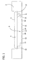
- Modified susceptor 2 has an inner annular ledge 22 which is capable of supporting semiconductor wafer 4 which has a front surface 6 and a back surface 8.
- Modified susceptor 2 has a porous surface 9 with a plurality of holes or openings 10, 11, 12, 13, 14, 16, and 18 and wafer lift pin hole 21.
- the terms openings and holes may be used interchangeably herein and both refer to the open passageways in the porous surface 9.
- Porous surface 9 having the openings is located directly below the semiconductor wafer 4.
- the term "plurality" means two or more holes.
- Holes 10, 11, 12, 13, 14, 16, and 18 are drilled into modified susceptor 2 prior to the coating being applied.
- holes 10, 11, 12, 13, 14, 16, and 18 allow the cleaning gas to contact substantially the entire back surface 8 of semiconductor wafer 4 to allow the cleaning gas to react with, and remove substantially all native oxide on the back surface 8 of semiconductor wafer 4.
- the portion of back surface 8 of semiconductor wafer 4 in contact with the inner annular ledge 22 of susceptor 2 is also substantially etched by the cleaning gas as the gas will effuse between the wafer and the susceptor resulting in substantially complete removal of the native oxide layer on the back surface.
- the removal of the native oxide from the back surface 8 significantly reduces or eliminates any halo effect on the back surface of the semiconductor wafer as any source gas that effuses between the wafer and the susceptor during the epitaxial growth process and contacts back surface 8 will grow smoothly and continuously on top of the silicon surface.
- Holes 10, 11, 12, 13, 14, 16, and 18 also allow dopant atoms that out-diffuse from the back surface 8 of semiconductor wafer 4 during the high temperature cleaning step and epitaxial deposition step of an epitaxial deposition process to drain through the holes into a purge gas or hydrogen stream and away from the front surface 6 of semiconductor wafer 4 into the exhaust system. As such, a significant reduction in autodoping of the front surface during an epitaxial deposition process is realized.
- FIG. 2 there is shown a top view of modified susceptor 2 having inner annular ledge 22 and porous surface 24 having a plurality of holes.
- Wafer lift pin holes 28, 30, and 32 on porous surface 24 allow lift pins (not shown) below the modified susceptor 2 to raise and lower semiconductor wafers onto and off of the modified susceptor during and after an epitaxial deposition process.
- Edge ring 26 surrounds the periphery of modified susceptor 2 and is utilized throughout an epitaxial deposition process to ensure temperature uniformity across a semiconductor wafer such that a temperature gradient does not form across the wafer and adversely affect the deposition process.
- Edge ring 26 generally has a diameter 4 centimeters to about 10 centimeters greater than the diameter of modified susceptor 2 and is comprised of high purity graphite which has a silicon carbide or glassy carbon coating.
- the modified susceptor for use in the process of the present invention can be sized and configured such that the inner annular ledge of the susceptor can accommodate any diameter semiconductor wafer including, for example, 150 millimeter, 200 millimeter and 300 millimeter wafers.
- the modified susceptor may be constructed of conventional materials such as high purity graphite and has a silicon carbide or glassy carbon layer covering the graphite to reduce the amount of contaminants released into the surrounding ambient from the graphite during the high temperature epitaxial deposition process.
- the graphite utilized to construct the susceptor is generally at least about 99%, more preferably at least about 99.9% and most preferably at least about 99.99% pure graphite.
- the graphite preferably contains less than about 20 ppm total metals such as iron, molybdenum, copper, and nickel, and more preferably less that about 5 ppm total metals such as iron, molybdenum, copper, and nickel.
- the silicon carbide or glassy carbon coating covering the graphite generally has a thickness of between about 75 micrometers and about 150 micrometers, preferably about 125 micrometers.
- the holes in the porous surface of the modified susceptor located directly below the semiconductor wafer preferably have a diameter such that the silicon carbide or glassy carbon coating, if applied to the susceptor after the holes have been drilled into the susceptor, will not substantially block or plug the holes and thus restrict fluid flow therethrough.
- the openings generally referred to as holes throughout, could be squares, slots, diamond shapes, or any other shapes allowing fluid flow therethrough.
- the openings preferably have a width of between about 0.1 millimeters and about 3 millimeters, more preferably between about 0.1 millimeters and about 1 millimeter, and most preferably between about 0.5 millimeters and about 1 millimeter.
- the width of the openings is defined as the greatest distance between two corners of the opening or the diameter if the opening is a circle.
- the holes are spaced on the modified susceptor to allow the cleaning gas utilized during the pre-bake step of the epitaxial deposition process to contact and etch substantially the entire back surface of the semiconductor wafer. Spacing of the holes of the modified susceptor of between about 0.5 millimeters and about 4 centimeters apart, more preferably between about 2 millimeters and about 2 centimeters apart, and most preferably between about 6 millimeters and about 1.5 centimeters apart allows the cleaning gas to contact substantially the entire back surface of the semiconductor wafer such that it may etch substantially all of the native oxide from the back surface.
- the total percentage of open area on the surface of the susceptor is between about 0.5% and about 4% of the total surface area of the susceptor, more preferably between about 1% and about 3% of the total surface area of the susceptor.
- the surface of the susceptor preferably has a density of between about 0.2 holes/cm 2 and about 4 holes/cm 2 , more preferably between about 0.8 holes/cm 2 and about 1.75 holes/cm 2 . Density as used herein means either a uniform or non-uniform density.
- the holes in the modified susceptor have as small a diameter as practical yet not allow the silicon carbide or glassy carbon coating to restrict fluid flow through the holes to the back surface of the semiconductor wafer. If the holes in the susceptor are drilled too large, nanotopology problems on the front surface of the wafer that are caused by localized temperature non-uniformity on the back surface can occur. Large diameter holes in the modified susceptor can lead to the development of hot spots or cold spots on the back surface of the semiconductor wafer through direct irradiation of the back surface by the heating lamps located below the semiconductor wafer. These hot or cold spots cause temperature gradients to form across the front surface of the semiconductor wafer and can lead to non-uniform epitaxial silicon growth on the front surface of the semiconductor wafer.
- Non-uniform growth of the epitaxial layer significantly degrades the wafer quality.
- the holes on the modified susceptor can be drilled into the susceptor at an oblique angle to further reduce the possibility of direct irradiation of the back surface by the heating lamps and the formation of hot or cold spots leading to non-uniform epitaxial growth on the front surface yet still allow gases to penetrate the susceptor and contact the back surface and allow out-diffused dopant atoms to move away from the back surface.
- the lamp power ratio of the heating lamps above and below the semiconductor wafer can be adjusted and tuned to produce a balanced heating from the lamps.
- the modified susceptor of the present invention may be utilized as part of an apparatus for chemical vapor deposition processes such as an epitaxial deposition processes.
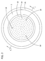
- Fig. 3 there is shown an epitaxial reaction chamber 34 for use during an epitaxial growth process utilizing the modified susceptor 36 of the present invention.
- Modified susceptor 36 is attached to rotatable support means 58 and 59 and is sized and configured to support semiconductor wafer 38 on inner annular ledge 42 during an epitaxial deposition process.
- Semiconductor wafer 38 is in spaced relationship with holes 44, 45, 46, 47, 48, 49, and 51 in porous surface 49 in modified susceptor 36.
- Lift pin hole 62 allows a lift pin (not shown) access through porous surface 9 of modified susceptor 36 to semiconductor wafer 38 such that semiconductor wafer 3 8 may be lifted onto and off of modified susceptor 36 before and after an epitaxial deposition process.
- Epitaxial deposition chamber 34 also contains heating lamp arrays 50 and 52 located above and below modified susceptor 36 respectively for heating during an epitaxial deposition process.
- Gas inlets 54 and 56 allow the introduction of the cleaning gas during the prebake step of the epitaxial deposition process such that cleaning gas is introduced above and below the semiconductor wafer 38 to enhance the native oxide removal of the front surface 60 and back surface 62 of semiconductor wafer 38.
- gas inlet 54 introduces a silicon containing source gas which is flowed above the wafer 38 and gas inlet 56 introduces hydrogen or an inert gas below the wafer 38 to flush the back surface 62 of the semiconductor wafer 38 and carry out-diffused dopant atoms away from the front surface.
- gas injected into the epitaxial deposition chamber flows parallel to the front and back surfaces of the semiconductor wafer. Such a flow pattern allows the injected gases to contact the front surface and penetrate the susceptor through the holes in the susceptor's surface to contact the back surface of the wafer.
- the holes in the modified susceptor will allow the cleaning gas to pass through the modified susceptor and contact substantially the entire back surface of the semiconductor wafer during the cleaning step such that any native oxide present on the back surface will be removed by the cleaning gas.
- This native oxide removal from the back surface will allow a smooth, continuous epitaxial silicon layer to grow on any portion of the back surface of the semiconductor wafer that is contacted with the source gas during the growth of the epitaxial layer and thus will substantially eliminate the formation of any halo on the back surface.
- the holes in the modified susceptor will allow inert gas or hydrogen to contact the back surface of the wafer such that dopant atoms that out-diffuse from the back surface during both the cleaning step and the epitaxial growth step may be carried away from the semiconductor wafer and into the exhaust thus substantially decreasing the possibility of autodoping the front surface of the wafer.
- the epitaxial reaction chamber containing the modified susceptor of the present invention described above may be utilized for both the cleaning and the growth steps of an epitaxial deposition process.
- an epitaxial silicon layer is grown on the front surface of a semiconductor wafer.
- a silicon wafer is introduced into an epitaxial deposition chamber at ambient pressure and a cleaning gas such as hydrogen or a mixture of hydrogen and hydrochloric acid is introduced into the chamber at a temperature of between about 1000°C and about 1300°C at a flow rate of between about 1 liter/minute and about 50 liters/minute, preferably between about 10 liters/minute and about 20 liters/minute for at least about 10 seconds to remove the native oxide layers on the front and back surfaces of the semiconductor wafer.
- a cleaning gas such as hydrogen or a mixture of hydrogen and hydrochloric acid
- the cleaning gas is discontinued and the temperature in the reaction chamber is adjusted to between about 600°C and about 1200°C and a silicon containing source gas such as silane or dichlorosilane, for example, is introduced above the front surface of the semiconductor wafer at a flow rate of between about 1 liter/minute and about 20 liters/minute for a period of time sufficient to grow an epitaxial silicon layer on the front surface of the semiconductor wafer having a thickness of between about 0.1 and about 200 micrometers, preferably between about 1 and about 100 micrometers.
- a silicon containing source gas such as silane or dichlorosilane
- a gas such as nitrogen, argon, hydrogen, a mixture thereof or the source gas is introduced below the back surface of the semiconductor wafer at a flow rate of between about 1 liter/minute and about 50 liters/minute, preferably between about 10 liters/minute and about 20 liters/minute such that the purge gas can contact the back surface of the semiconductor wafer and carry out-diffused dopant atoms from the back surface toward to the exhaust outlet.
- This preferred embodiment significantly reduces or eliminates any back surface halo effect and minimizes autodoping of the front surface.
- the preferred epitaxial deposition process is carried out at ambient pressure, reduced pressure chemical vapor deposition is also within the scope of the present invention.
- the modified susceptor may be sized and configured to allow the semiconductor wafer to rest directly on the porous surface thus eliminating the inner annular ledge 22 as shown in Fig. 1 .
- Fig. 4 there is shown a cross section of a modified susceptor where the semiconductor wafer rests directly upon the porous surface.
- the back surface 76 of semiconductor wafer 70 sits directly on porous surface 72 of modified susceptor 74.
- back surface 76 of wafer 70 is in direct contact with the porous surface 72, gases flowed beneath modified susceptor 74 are able to penetrate porous surface 72 through holes 78, 80, 82, 84, 86, 88, and 90 and contact substantially the entire back surface 76 of wafer 70.
- the modified susceptor for use in the process of the present invention as illustrated in Fig. 4 may be further modified such that porous surface 72 is shaped in a dish or dome shape to allow only the outer edges of the semiconductor wafer to contact the modified susceptor.
- Fig. 5 there is shown a cross section of a modified susceptor where the semiconductor wafer rests directly on the porous surface of the susceptor. The back surface 76 of semiconductor wafer 70 sits directly on porous surface 72 of modified susceptor 74.
- Porous surface 72 is shaped like a dish or dome such that the outer edges 92 and 94 of semiconductor wafer 70 are in direct contact with the porous surface 72 and the remainder of back surface 76 or wafer 70 is not in direct contact with porous surface 72.
- holes 78, 80, 82, 84, 86, 88, and 90 allow fluid flow therethrough to the back surface of the wafer.
- modified susceptor for use in the process of the present invention can be utilized with various types of deposition reactors including barrel, pancake and mini batch reactors regardless of the shape of the susceptor utilized.
Landscapes
- Chemical & Material Sciences (AREA)
- Engineering & Computer Science (AREA)
- Organic Chemistry (AREA)
- Materials Engineering (AREA)
- Metallurgy (AREA)
- Chemical Kinetics & Catalysis (AREA)
- General Chemical & Material Sciences (AREA)
- Mechanical Engineering (AREA)
- Crystallography & Structural Chemistry (AREA)
- Physics & Mathematics (AREA)
- Condensed Matter Physics & Semiconductors (AREA)
- General Physics & Mathematics (AREA)
- Manufacturing & Machinery (AREA)
- Computer Hardware Design (AREA)
- Microelectronics & Electronic Packaging (AREA)
- Power Engineering (AREA)
- Chemical Vapour Deposition (AREA)
- Crystals, And After-Treatments Of Crystals (AREA)
Applications Claiming Priority (3)
| Application Number | Priority Date | Filing Date | Title |
|---|---|---|---|
| US566890 | 2000-05-08 | ||
| US09/566,890 US6444027B1 (en) | 2000-05-08 | 2000-05-08 | Modified susceptor for use in chemical vapor deposition process |
| PCT/US2001/012668 WO2001086034A2 (en) | 2000-05-08 | 2001-04-19 | Modified susceptor for use in chemical vapor deposition process |
Publications (2)
| Publication Number | Publication Date |
|---|---|
| EP1287187A2 EP1287187A2 (en) | 2003-03-05 |
| EP1287187B1 true EP1287187B1 (en) | 2009-06-17 |
Family
ID=24264828
Family Applications (1)
| Application Number | Title | Priority Date | Filing Date |
|---|---|---|---|
| EP01930582A Expired - Lifetime EP1287187B1 (en) | 2000-05-08 | 2001-04-19 | Chemical vapor deposition process |
Country Status (8)
Families Citing this family (125)
| Publication number | Priority date | Publication date | Assignee | Title |
|---|---|---|---|---|
| US6113702A (en) * | 1995-09-01 | 2000-09-05 | Asm America, Inc. | Wafer support system |
| US6183565B1 (en) * | 1997-07-08 | 2001-02-06 | Asm International N.V | Method and apparatus for supporting a semiconductor wafer during processing |
| US6444027B1 (en) * | 2000-05-08 | 2002-09-03 | Memc Electronic Materials, Inc. | Modified susceptor for use in chemical vapor deposition process |
| DE10027931C1 (de) * | 2000-05-31 | 2002-01-10 | Infineon Technologies Ag | Verfahren zur rückseitigen elektrischen Kontaktierung eines Halbleitersubstrats während seiner Bearbeitung |
| US6599815B1 (en) * | 2000-06-30 | 2003-07-29 | Memc Electronic Materials, Inc. | Method and apparatus for forming a silicon wafer with a denuded zone |
| US6822945B2 (en) | 2000-11-08 | 2004-11-23 | Genesys Telecommunications Laboratories, Inc. | Method and apparatus for anticipating and planning communication-center resources based on evaluation of events waiting in a communication center master queue |
| US6576572B2 (en) * | 2000-12-28 | 2003-06-10 | Schott Lithotec Ag | Method of heating a substrate using a variable surface hot plate for improved bake uniformity |
| DE10111761A1 (de) * | 2001-03-12 | 2002-10-02 | Infineon Technologies Ag | Anordnung und Verfahren zum rückseitigen Kontaktieren eines Halbleitersubstrats |
| JP2003229370A (ja) * | 2001-11-30 | 2003-08-15 | Shin Etsu Handotai Co Ltd | サセプタ、気相成長装置、エピタキシャルウェーハの製造方法およびエピタキシャルウェーハ |
| EP1460679A1 (en) * | 2001-11-30 | 2004-09-22 | Shin-Etsu Handotai Co., Ltd | Susceptor, gaseous phase growing device, device and method for manufacturing epitaxial wafer, and epitaxial wafer |
| JP4061062B2 (ja) * | 2001-12-13 | 2008-03-12 | ローム株式会社 | 半導体発光素子の製法および酸化炉 |
| JP2003197532A (ja) * | 2001-12-21 | 2003-07-11 | Sumitomo Mitsubishi Silicon Corp | エピタキシャル成長方法及びエピタキシャル成長用サセプター |
| US20050000449A1 (en) * | 2001-12-21 | 2005-01-06 | Masayuki Ishibashi | Susceptor for epitaxial growth and epitaxial growth method |
| DE10211312A1 (de) | 2002-03-14 | 2003-10-02 | Wacker Siltronic Halbleitermat | Verfahren und Vorrichtung zur epitaktischen Beschichtung einer Halbleiterscheibe sowie epitaktisch beschichtete Halbleiterscheibe |
| JP4089354B2 (ja) * | 2002-08-30 | 2008-05-28 | 株式会社Sumco | エピタキシャルウェーハとその製造方法 |
| JP4016823B2 (ja) * | 2002-12-06 | 2007-12-05 | 信越半導体株式会社 | シリコンエピタキシャルウェーハの製造方法 |
| DE10261362B8 (de) * | 2002-12-30 | 2008-08-28 | Osram Opto Semiconductors Gmbh | Substrat-Halter |
| US20060225642A1 (en) * | 2003-03-31 | 2006-10-12 | Yoshihiko Kanzawa | Method of forming semiconductor crystal |
| US7064073B1 (en) * | 2003-05-09 | 2006-06-20 | Newport Fab, Llc | Technique for reducing contaminants in fabrication of semiconductor wafers |
| JP4066881B2 (ja) * | 2003-05-21 | 2008-03-26 | 信越半導体株式会社 | 表面処理方法、シリコンエピタキシャルウェーハの製造方法及びシリコンエピタキシャルウェーハ |
| DE10328842B4 (de) * | 2003-06-26 | 2007-03-01 | Siltronic Ag | Suszeptor für eine chemische Gasphasenabscheidung, Verfahren zur Bearbeitung einer Halbleiterscheibe durch chemische Gasphasenabscheidung und nach dem Verfahren bearbeitete Halbleiterscheibe |
| KR101144825B1 (ko) * | 2003-06-26 | 2012-05-11 | 신에쯔 한도타이 가부시키가이샤 | 실리콘 에피택셜 웨이퍼의 제조 방법 및 실리콘 에피택셜 웨이퍼 |
| DE102004060625A1 (de) * | 2004-12-16 | 2006-06-29 | Siltronic Ag | Beschichtete Halbleiterscheibe und Verfahren und Vorrichtung zur Herstellung der Halbleiterscheibe |
| US7285483B2 (en) * | 2003-06-26 | 2007-10-23 | Silitronic Ag | Coated semiconductor wafer, and process and apparatus for producing the semiconductor wafer |
| CN1864245A (zh) * | 2003-10-01 | 2006-11-15 | 信越半导体株式会社 | 硅外延片的制造方法及硅外延片 |
| US7323058B2 (en) * | 2004-01-26 | 2008-01-29 | Applied Materials, Inc. | Apparatus for electroless deposition of metals onto semiconductor substrates |
| US7827930B2 (en) * | 2004-01-26 | 2010-11-09 | Applied Materials, Inc. | Apparatus for electroless deposition of metals onto semiconductor substrates |
| US7654221B2 (en) * | 2003-10-06 | 2010-02-02 | Applied Materials, Inc. | Apparatus for electroless deposition of metals onto semiconductor substrates |
| US7166528B2 (en) | 2003-10-10 | 2007-01-23 | Applied Materials, Inc. | Methods of selective deposition of heavily doped epitaxial SiGe |
| US7235139B2 (en) * | 2003-10-28 | 2007-06-26 | Veeco Instruments Inc. | Wafer carrier for growing GaN wafers |
| DE10357698A1 (de) * | 2003-12-09 | 2005-07-14 | Schunk Kohlenstofftechnik Gmbh | Träger für zu behandelnde Gegenstände sowie Verfahren zur Herstellung eines solchen |
| US7648579B2 (en) * | 2004-02-13 | 2010-01-19 | Asm America, Inc. | Substrate support system for reduced autodoping and backside deposition |
| US20050193951A1 (en) * | 2004-03-08 | 2005-09-08 | Muneo Furuse | Plasma processing apparatus |
| JP4636807B2 (ja) * | 2004-03-18 | 2011-02-23 | キヤノン株式会社 | 基板保持装置およびそれを用いた露光装置 |
| JPWO2005093136A1 (ja) * | 2004-03-29 | 2008-02-14 | エピクルー株式会社 | 支持体並びに半導体基板の処理方法 |
| US20050217585A1 (en) * | 2004-04-01 | 2005-10-06 | Blomiley Eric R | Substrate susceptor for receiving a substrate to be deposited upon |
| US20050217569A1 (en) * | 2004-04-01 | 2005-10-06 | Nirmal Ramaswamy | Methods of depositing an elemental silicon-comprising material over a semiconductor substrate and methods of cleaning an internal wall of a chamber |
| US20050223985A1 (en) * | 2004-04-08 | 2005-10-13 | Blomiley Eric R | Deposition apparatuses, methods of assessing the temperature of semiconductor wafer substrates within deposition apparatuses, and methods for deposition of epitaxial semiconductive material |
| US20050223993A1 (en) * | 2004-04-08 | 2005-10-13 | Blomiley Eric R | Deposition apparatuses; methods for assessing alignments of substrates within deposition apparatuses; and methods for assessing thicknesses of deposited layers within deposition apparatuses |
| JP2005333090A (ja) * | 2004-05-21 | 2005-12-02 | Sumco Corp | P型シリコンウェーハおよびその熱処理方法 |
| JP2006040972A (ja) * | 2004-07-22 | 2006-02-09 | Shin Etsu Handotai Co Ltd | シリコンエピタキシャルウェーハおよびその製造方法 |
| JP4304720B2 (ja) * | 2004-07-30 | 2009-07-29 | 信越半導体株式会社 | サセプタ、気相成長装置、エピタキシャルウェーハの製造方法およびエピタキシャルウェーハ |
| US7250358B2 (en) * | 2004-08-06 | 2007-07-31 | Globitech Incorporated | Wafer for preventing the formation of silicon nodules and method for preventing the formation of silicon nodules |
| KR100678468B1 (ko) * | 2005-01-14 | 2007-02-02 | 삼성전자주식회사 | 반도체 기판의 인-시츄 세정방법 및 이를 채택하는 반도체소자의 제조방법 |
| US7198677B2 (en) * | 2005-03-09 | 2007-04-03 | Wafermasters, Inc. | Low temperature wafer backside cleaning |
| US7462246B2 (en) * | 2005-04-15 | 2008-12-09 | Memc Electronic Materials, Inc. | Modified susceptor for barrel reactor |
| US7474114B2 (en) * | 2005-09-08 | 2009-01-06 | Sitronic Corporation | System and method for characterizing silicon wafers |
| KR100794719B1 (ko) * | 2005-11-02 | 2008-01-15 | 주식회사 실트론 | 화학 기상 증착 장치용 서셉터 |
| US7485928B2 (en) * | 2005-11-09 | 2009-02-03 | Memc Electronic Materials, Inc. | Arsenic and phosphorus doped silicon wafer substrates having intrinsic gettering |
| TWI354320B (en) * | 2006-02-21 | 2011-12-11 | Nuflare Technology Inc | Vopor phase deposition apparatus and support table |
| US7566951B2 (en) | 2006-04-21 | 2009-07-28 | Memc Electronic Materials, Inc. | Silicon structures with improved resistance to radiation events |
| US20070282471A1 (en) * | 2006-06-01 | 2007-12-06 | Integrated System Solution Corp. | Bluetooth audio chip with multiple input/output sources |
| CN100392815C (zh) * | 2006-06-02 | 2008-06-04 | 河北工业大学 | 能消除硅气相外延层中滑移线与高应力区的装置 |
| US8852349B2 (en) * | 2006-09-15 | 2014-10-07 | Applied Materials, Inc. | Wafer processing hardware for epitaxial deposition with reduced auto-doping and backside defects |
| US8951351B2 (en) * | 2006-09-15 | 2015-02-10 | Applied Materials, Inc. | Wafer processing hardware for epitaxial deposition with reduced backside deposition and defects |
| DE102006055038B4 (de) * | 2006-11-22 | 2012-12-27 | Siltronic Ag | Epitaxierte Halbleiterscheibe sowie Vorrichtung und Verfahren zur Herstellung einer epitaxierten Halbleiterscheibe |
| CN101241854B (zh) * | 2007-02-06 | 2011-06-01 | 中芯国际集成电路制造(上海)有限公司 | 一种晶圆生产工艺 |
| US8083963B2 (en) * | 2007-02-08 | 2011-12-27 | Applied Materials, Inc. | Removal of process residues on the backside of a substrate |
| US7605054B2 (en) * | 2007-04-18 | 2009-10-20 | S.O.I.Tec Silicon On Insulator Technologies | Method of forming a device wafer with recyclable support |
| US20080314319A1 (en) * | 2007-06-19 | 2008-12-25 | Memc Electronic Materials, Inc. | Susceptor for improving throughput and reducing wafer damage |
| DE102008010041A1 (de) * | 2007-09-28 | 2009-04-02 | Osram Opto Semiconductors Gmbh | Schichtabscheidevorrichtung und Verfahren zu deren Betrieb |
| US20090165721A1 (en) * | 2007-12-27 | 2009-07-02 | Memc Electronic Materials, Inc. | Susceptor with Support Bosses |
| US8404049B2 (en) * | 2007-12-27 | 2013-03-26 | Memc Electronic Materials, Inc. | Epitaxial barrel susceptor having improved thickness uniformity |
| JP5396737B2 (ja) * | 2008-04-04 | 2014-01-22 | 株式会社Sumco | エピタキシャルシリコンウェーハ及びその製造方法 |
| US20090280248A1 (en) * | 2008-05-06 | 2009-11-12 | Asm America, Inc. | Porous substrate holder with thinned portions |
| DE102008023054B4 (de) * | 2008-05-09 | 2011-12-22 | Siltronic Ag | Verfahren zur Herstellung einer epitaxierten Halbleiterscheibe |
| JP5380912B2 (ja) * | 2008-06-10 | 2014-01-08 | 株式会社Sumco | 膜厚測定方法、エピタキシャルウェーハの製造方法、および、エピタキシャルウェーハ |
| CN101676203B (zh) | 2008-09-16 | 2015-06-10 | 储晞 | 生产高纯颗粒硅的方法 |
| JP2010098284A (ja) * | 2008-09-19 | 2010-04-30 | Covalent Materials Corp | エピタキシャル基板用シリコンウェハの製造方法及びエピタキシャル基板の製造方法 |
| JP5271648B2 (ja) * | 2008-09-22 | 2013-08-21 | 株式会社ニューフレアテクノロジー | 半導体製造方法および半導体製造装置 |
| US20100098519A1 (en) * | 2008-10-17 | 2010-04-22 | Memc Electronic Materials, Inc. | Support for a semiconductor wafer in a high temperature environment |
| KR101543273B1 (ko) | 2008-10-27 | 2015-08-12 | 주성엔지니어링(주) | 기판처리장치 |
| US8151852B2 (en) | 2009-06-30 | 2012-04-10 | Twin Creeks Technologies, Inc. | Bonding apparatus and method |
| JP5795461B2 (ja) * | 2009-08-19 | 2015-10-14 | 株式会社Sumco | エピタキシャルシリコンウェーハの製造方法 |
| US9127364B2 (en) | 2009-10-28 | 2015-09-08 | Alta Devices, Inc. | Reactor clean |
| JP5544859B2 (ja) * | 2009-12-15 | 2014-07-09 | 信越半導体株式会社 | シリコンエピタキシャルウェーハの製造方法 |
| KR101125739B1 (ko) * | 2010-02-03 | 2012-03-27 | 주식회사 엘지실트론 | 반도체 제조용 서셉터 |
| US9650726B2 (en) | 2010-02-26 | 2017-05-16 | Applied Materials, Inc. | Methods and apparatus for deposition processes |
| US9181619B2 (en) * | 2010-02-26 | 2015-11-10 | Fujifilm Corporation | Physical vapor deposition with heat diffuser |
| US20110239933A1 (en) * | 2010-04-01 | 2011-10-06 | Bernhard Freudenberg | Device and method for the production of silicon blocks |
| US9570328B2 (en) | 2010-06-30 | 2017-02-14 | Applied Materials, Inc. | Substrate support for use with multi-zonal heating sources |
| US8535445B2 (en) * | 2010-08-13 | 2013-09-17 | Veeco Instruments Inc. | Enhanced wafer carrier |
| KR20120071695A (ko) * | 2010-12-23 | 2012-07-03 | 삼성엘이디 주식회사 | 화학 기상 증착 장치용 서셉터, 화학 기상 증착 장치 및 화학 기상 증착 장치를 이용한 기판의 가열 방법 |
| WO2012092064A1 (en) * | 2010-12-30 | 2012-07-05 | Veeco Instruments Inc. | Wafer processing with carrier extension |
| KR101238841B1 (ko) * | 2011-01-04 | 2013-03-04 | 주식회사 엘지실트론 | 화학 기상 증착 장치용 서셉터 및 이를 갖는 화학 기상 증착 장치 |
| WO2012102755A1 (en) * | 2011-01-28 | 2012-08-02 | Applied Materials, Inc. | Carbon addition for low resistivity in situ doped silicon epitaxy |
| CN102851735B (zh) * | 2011-06-28 | 2015-08-19 | 上海华虹宏力半导体制造有限公司 | 化学气相淀积硅外延生长方法 |
| JP5780062B2 (ja) * | 2011-08-30 | 2015-09-16 | 東京エレクトロン株式会社 | 基板処理装置及び成膜装置 |
| CN102412271A (zh) * | 2011-09-15 | 2012-04-11 | 上海晶盟硅材料有限公司 | 外延片衬底、外延片及半导体器件 |
| US8940094B2 (en) | 2012-04-10 | 2015-01-27 | Sunedison Semiconductor Limited | Methods for fabricating a semiconductor wafer processing device |
| US9401271B2 (en) | 2012-04-19 | 2016-07-26 | Sunedison Semiconductor Limited (Uen201334164H) | Susceptor assemblies for supporting wafers in a reactor apparatus |
| WO2013162972A1 (en) * | 2012-04-25 | 2013-10-31 | Applied Materials, Inc. | Process chamber having separate process gas and purge gas regions |
| JP5845143B2 (ja) * | 2012-06-29 | 2016-01-20 | 株式会社Sumco | エピタキシャルシリコンウェーハの製造方法、および、エピタキシャルシリコンウェーハ |
| US11326255B2 (en) * | 2013-02-07 | 2022-05-10 | Uchicago Argonne, Llc | ALD reactor for coating porous substrates |
| CN107557758A (zh) * | 2013-05-01 | 2018-01-09 | 应用材料公司 | 用于控制外延沉积腔室流量的注入及排放设计 |
| EP3100298B1 (en) | 2014-01-27 | 2020-07-15 | Veeco Instruments Inc. | Wafer carrier having retention pockets with compound radii for chemical vapor deposition systems |
| CN204434500U (zh) * | 2015-03-05 | 2015-07-01 | 京东方科技集团股份有限公司 | 一种蒸镀载板及蒸镀装置 |
| WO2016154052A1 (en) | 2015-03-25 | 2016-09-29 | Applied Materials, Inc. | Chamber components for epitaxial growth apparatus |
| JP6447351B2 (ja) * | 2015-05-08 | 2019-01-09 | 株式会社Sumco | シリコンエピタキシャルウェーハの製造方法およびシリコンエピタキシャルウェーハ |
| US10184193B2 (en) | 2015-05-18 | 2019-01-22 | Globalwafers Co., Ltd. | Epitaxy reactor and susceptor system for improved epitaxial wafer flatness |
| US20160342147A1 (en) | 2015-05-19 | 2016-11-24 | Applied Materials, Inc. | Methods and systems for applying run-to-run control and virtual metrology to reduce equipment recovery time |
| DE102016210203B3 (de) * | 2016-06-09 | 2017-08-31 | Siltronic Ag | Suszeptor zum Halten einer Halbleiterscheibe, Verfahren zum Abscheiden einer epitaktischen Schicht auf einer Vorderseite einer Halbleiterscheibe und Halbleiterscheibe mit epitaktischer Schicht |
| CN107546101A (zh) * | 2016-06-23 | 2018-01-05 | 上海新昇半导体科技有限公司 | 一种外延生长方法 |
| US20180102247A1 (en) * | 2016-10-06 | 2018-04-12 | Asm Ip Holding B.V. | Substrate processing apparatus and method of manufacturing semiconductor device |
| CN108728898A (zh) * | 2017-04-24 | 2018-11-02 | 上海新昇半导体科技有限公司 | 一种外延炉硅片基座 |
| CN109811406B (zh) * | 2017-11-20 | 2021-09-17 | 北京北方华创微电子装备有限公司 | 石英件、工艺腔室和半导体处理设备 |
| US10991617B2 (en) * | 2018-05-15 | 2021-04-27 | Applied Materials, Inc. | Methods and apparatus for cleaving of semiconductor substrates |
| JP7321768B2 (ja) | 2018-05-23 | 2023-08-07 | 信越化学工業株式会社 | 化学気相成長装置および被膜形成方法 |
| JP6998839B2 (ja) * | 2018-06-25 | 2022-01-18 | グローバルウェーハズ・ジャパン株式会社 | エピタキシャルシリコンウェーハの製造方法 |
| KR102620219B1 (ko) * | 2018-11-02 | 2024-01-02 | 삼성전자주식회사 | 기판 처리 방법 및 기판 처리 장치 |
| DE102019132933A1 (de) * | 2018-12-10 | 2020-06-10 | Showa Denko K.K. | Suszeptor und vorrichtung zur chemischen gasphasenabscheidung |
| CN112309950B (zh) * | 2019-07-26 | 2023-01-17 | 上海宏轶电子科技有限公司 | 一种晶圆清洗机用机台 |
| JP7192756B2 (ja) * | 2019-12-19 | 2022-12-20 | 株式会社Sumco | 気相成長装置及び気相成長方法 |
| US11111578B1 (en) | 2020-02-13 | 2021-09-07 | Uchicago Argonne, Llc | Atomic layer deposition of fluoride thin films |
| CN111599746B (zh) * | 2020-07-27 | 2020-10-30 | 西安奕斯伟硅片技术有限公司 | 一种用于晶片的外延生长的基座、装置及方法 |
| KR20230027251A (ko) * | 2020-11-19 | 2023-02-27 | 어플라이드 머티어리얼스, 인코포레이티드 | 기판 극단 에지 보호를 위한 링 |
| KR102582346B1 (ko) * | 2021-03-30 | 2023-09-25 | 에스케이실트론 주식회사 | 웨이퍼의 에피택셜층 성장 방법 |
| US12394659B2 (en) * | 2021-04-30 | 2025-08-19 | Asm Ip Holding B.V. | Susceptors with film deposition control features |
| US20220364263A1 (en) * | 2021-05-12 | 2022-11-17 | Applied Materials, Inc. | Low mass substrate support |
| CN113529165B (zh) * | 2021-07-21 | 2024-08-16 | 青岛佳恩半导体有限公司 | 一种超薄衬底外延生长装置及制备方法 |
| US12065738B2 (en) | 2021-10-22 | 2024-08-20 | Uchicago Argonne, Llc | Method of making thin films of sodium fluorides and their derivatives by ALD |
| US11901169B2 (en) | 2022-02-14 | 2024-02-13 | Uchicago Argonne, Llc | Barrier coatings |
| JP2023134139A (ja) * | 2022-03-14 | 2023-09-27 | キオクシア株式会社 | 半導体製造装置 |
| US20240145230A1 (en) * | 2022-10-28 | 2024-05-02 | Applied Materials, Inc. | Semiconductor cleaning using plasma-free precursors |
| US20240247405A1 (en) * | 2023-01-24 | 2024-07-25 | Applied Materials, Inc. | Method for controlling layer-to-layer thickness in multi-tier epitaxial process |
Family Cites Families (30)
| Publication number | Priority date | Publication date | Assignee | Title |
|---|---|---|---|---|
| US4496609A (en) | 1969-10-15 | 1985-01-29 | Applied Materials, Inc. | Chemical vapor deposition coating process employing radiant heat and a susceptor |
| US4322592A (en) | 1980-08-22 | 1982-03-30 | Rca Corporation | Susceptor for heating semiconductor substrates |
| JPS58130518A (ja) | 1982-01-29 | 1983-08-04 | Toshiba Corp | 気相成長方法 |
| US5242501A (en) | 1982-09-10 | 1993-09-07 | Lam Research Corporation | Susceptor in chemical vapor deposition reactors |
| NL8602357A (nl) | 1985-10-07 | 1987-05-04 | Epsilon Ltd Partnership | Inrichting en werkwijze voor het chemisch uit damp neerslaan met gebruik van een axiaal symmetrische gasstroming. |
| US5200157A (en) | 1986-02-17 | 1993-04-06 | Toshiba Ceramics Co., Ltd. | Susceptor for vapor-growth deposition |
| US5177878A (en) | 1989-05-08 | 1993-01-12 | U.S. Philips Corporation | Apparatus and method for treating flat substrate under reduced pressure in the manufacture of electronic devices |
| DE3943482C2 (de) * | 1989-05-08 | 1994-07-07 | Balzers Hochvakuum | Werkstückträger für ein scheibenförmiges Werkstück, sowie Vakuumprozeßkammer |
| US5133284A (en) | 1990-07-16 | 1992-07-28 | National Semiconductor Corp. | Gas-based backside protection during substrate processing |
| US5192371A (en) | 1991-05-21 | 1993-03-09 | Asm Japan K.K. | Substrate supporting apparatus for a CVD apparatus |
| JP2921306B2 (ja) | 1992-11-20 | 1999-07-19 | 株式会社村田製作所 | コイル部品及びその製造方法 |
| US5695568A (en) * | 1993-04-05 | 1997-12-09 | Applied Materials, Inc. | Chemical vapor deposition chamber |
| JPH088198A (ja) | 1994-06-21 | 1996-01-12 | Sumitomo Sitix Corp | 気相成長装置用サセプター |
| JPH0897159A (ja) | 1994-09-29 | 1996-04-12 | Handotai Process Kenkyusho:Kk | エピタキシャル成長方法および成長装置 |
| JPH08236462A (ja) | 1995-03-01 | 1996-09-13 | Shin Etsu Handotai Co Ltd | 気相成長方法 |
| JP3725598B2 (ja) | 1996-01-12 | 2005-12-14 | 東芝セラミックス株式会社 | エピタキシャルウェハの製造方法 |
| JP3467960B2 (ja) | 1996-02-29 | 2003-11-17 | 信越半導体株式会社 | 半導体単結晶薄膜の製造方法および装置 |
| US5960555A (en) | 1996-07-24 | 1999-10-05 | Applied Materials, Inc. | Method and apparatus for purging the back side of a substrate during chemical vapor processing |
| JPH10144697A (ja) | 1996-11-06 | 1998-05-29 | Toshiba Ceramics Co Ltd | シリコンウエーハ及びその製造方法 |
| JP3336897B2 (ja) | 1997-02-07 | 2002-10-21 | 三菱住友シリコン株式会社 | 気相成長装置用サセプター |
| JPH1116844A (ja) | 1997-06-23 | 1999-01-22 | Sumitomo Metal Ind Ltd | エピタキシャルシリコンウェーハの製造方法と素材用ウェーハ |
| JPH11116844A (ja) | 1997-08-09 | 1999-04-27 | Elegant:Kk | アルミニウム及びアルミニウム合金用充填被覆材、これを用いたアルミニウム及びアルミニウム合金の被覆構造、接着構造及び成形体 |
| JPH1187250A (ja) | 1997-09-01 | 1999-03-30 | Inotetsuku Kk | 気相成長装置 |
| US6596086B1 (en) | 1998-04-28 | 2003-07-22 | Shin-Etsu Handotai Co., Ltd. | Apparatus for thin film growth |
| US6127286A (en) * | 1998-05-11 | 2000-10-03 | Lsi Logic Corporation | Apparatus and process for deposition of thin film on semiconductor substrate while inhibiting particle formation and deposition |
| EP1125008B1 (en) | 1998-10-14 | 2003-06-18 | MEMC Electronic Materials, Inc. | Thermally annealed, low defect density single crystal silicon |
| WO2000026949A1 (fr) | 1998-10-29 | 2000-05-11 | Shin-Etsu Handotai Co., Ltd. | Plaquette a semi-conducteur et son procede de fabrication |
| US6284384B1 (en) | 1998-12-09 | 2001-09-04 | Memc Electronic Materials, Inc. | Epitaxial silicon wafer with intrinsic gettering |
| US6184154B1 (en) | 1999-10-13 | 2001-02-06 | Seh America, Inc. | Method of processing the backside of a wafer within an epitaxial reactor chamber |
| US6444027B1 (en) * | 2000-05-08 | 2002-09-03 | Memc Electronic Materials, Inc. | Modified susceptor for use in chemical vapor deposition process |
-
2000
- 2000-05-08 US US09/566,890 patent/US6444027B1/en not_active Expired - Lifetime
- 2000-12-29 US US09/752,222 patent/US6596095B2/en not_active Expired - Fee Related
-
2001
- 2001-04-19 EP EP01930582A patent/EP1287187B1/en not_active Expired - Lifetime
- 2001-04-19 JP JP2001582617A patent/JP4492840B2/ja not_active Expired - Lifetime
- 2001-04-19 KR KR1020027015043A patent/KR100784001B1/ko not_active Expired - Fee Related
- 2001-04-19 WO PCT/US2001/012668 patent/WO2001086034A2/en active Application Filing
- 2001-04-19 CN CNB018108091A patent/CN1223709C/zh not_active Expired - Lifetime
- 2001-04-19 DE DE60139008T patent/DE60139008D1/de not_active Expired - Lifetime
- 2001-06-26 TW TW090110944A patent/TWI285936B/zh not_active IP Right Cessation
-
2002
- 2002-08-28 US US10/229,415 patent/US6652650B2/en not_active Expired - Lifetime
Also Published As
| Publication number | Publication date |
|---|---|
| WO2001086034A2 (en) | 2001-11-15 |
| DE60139008D1 (de) | 2009-07-30 |
| CN1223709C (zh) | 2005-10-19 |
| US20010037761A1 (en) | 2001-11-08 |
| KR20030086220A (ko) | 2003-11-07 |
| TWI285936B (en) | 2007-08-21 |
| CN1434884A (zh) | 2003-08-06 |
| US6596095B2 (en) | 2003-07-22 |
| JP2004522294A (ja) | 2004-07-22 |
| KR100784001B1 (ko) | 2007-12-07 |
| WO2001086034B1 (en) | 2002-05-10 |
| EP1287187A2 (en) | 2003-03-05 |
| US6652650B2 (en) | 2003-11-25 |
| US20030041799A1 (en) | 2003-03-06 |
| JP4492840B2 (ja) | 2010-06-30 |
| WO2001086034A3 (en) | 2002-02-21 |
| US6444027B1 (en) | 2002-09-03 |
Similar Documents
| Publication | Publication Date | Title |
|---|---|---|
| EP1287187B1 (en) | Chemical vapor deposition process | |
| EP1287188B1 (en) | Epitaxial silicon wafer free from autodoping and backside halo | |
| JP3908112B2 (ja) | サセプタ、エピタキシャルウェーハ製造装置及びエピタキシャルウェーハ製造方法 | |
| KR101077324B1 (ko) | 에피택셜 코팅 실리콘 웨이퍼의 제조 방법 | |
| EP0953659B1 (en) | Apparatus for thin film growth | |
| US20100107974A1 (en) | Substrate holder with varying density | |
| KR20090117610A (ko) | 에피텍샬방식으로 코팅된 반도체 웨이퍼를 제조하는 방법 | |
| JP2003273037A (ja) | Cvd反応器中で半導体ウェーハの表側をエピタキシャル被覆する方法、この種の被覆された半導体ウェーハおよびcvd反応器用サセプタ | |
| KR20240115127A (ko) | 에피텍셜 웨이퍼 제조 방법 | |
| US20010052324A1 (en) | Device for producing and processing semiconductor substrates | |
| JP2000012470A (ja) | 気相成長装置 | |
| JPH0782997B2 (ja) | 半導体ウェーハの製造方法 | |
| JPWO2005093136A1 (ja) | 支持体並びに半導体基板の処理方法 | |
| JP2002231634A (ja) | シリコンエピタキシャルウェーハ及びシリコンエピタキシャルウェーハの製造方法 | |
| US20220316090A1 (en) | Method for growing epitaxial layer on wafer | |
| KR101238842B1 (ko) | 반도체 제조용 서셉터 및 이를 포함한 에피택셜 성장 장치 | |
| KR101125739B1 (ko) | 반도체 제조용 서셉터 | |
| JPH06188198A (ja) | エピタキシャル成長法 | |
| JPH11121314A (ja) | 炭化ケイ素ウエハおよびその製造方法 | |
| JPH11121313A (ja) | 炭化ケイ素ウエハの製造方法および炭化ケイ素ウエハ |
Legal Events
| Date | Code | Title | Description |
|---|---|---|---|
| PUAI | Public reference made under article 153(3) epc to a published international application that has entered the european phase |
Free format text: ORIGINAL CODE: 0009012 |
|
| 17P | Request for examination filed |
Effective date: 20021114 |
|
| AK | Designated contracting states |
Kind code of ref document: A2 Designated state(s): AT BE CH CY DE DK ES FI FR GB GR IE IT LI LU MC NL PT SE TR |
|
| 17Q | First examination report despatched |
Effective date: 20031125 |
|
| RBV | Designated contracting states (corrected) |
Designated state(s): AT BE CH CY DE FR GB IT LI |
|
| RTI1 | Title (correction) |
Free format text: CHEMICAL VAPOR DEPOSITION PROCESS |
|
| GRAP | Despatch of communication of intention to grant a patent |
Free format text: ORIGINAL CODE: EPIDOSNIGR1 |
|
| RBV | Designated contracting states (corrected) |
Designated state(s): DE FR GB IT |
|
| GRAS | Grant fee paid |
Free format text: ORIGINAL CODE: EPIDOSNIGR3 |
|
| GRAA | (expected) grant |
Free format text: ORIGINAL CODE: 0009210 |
|
| AK | Designated contracting states |
Kind code of ref document: B1 Designated state(s): DE FR GB IT |
|
| REG | Reference to a national code |
Ref country code: GB Ref legal event code: FG4D |
|
| REF | Corresponds to: |
Ref document number: 60139008 Country of ref document: DE Date of ref document: 20090730 Kind code of ref document: P |
|
| PLBE | No opposition filed within time limit |
Free format text: ORIGINAL CODE: 0009261 |
|
| STAA | Information on the status of an ep patent application or granted ep patent |
Free format text: STATUS: NO OPPOSITION FILED WITHIN TIME LIMIT |
|
| 26N | No opposition filed |
Effective date: 20100318 |
|
| PGFP | Annual fee paid to national office [announced via postgrant information from national office to epo] |
Ref country code: GB Payment date: 20110426 Year of fee payment: 11 |
|
| PGFP | Annual fee paid to national office [announced via postgrant information from national office to epo] |
Ref country code: IT Payment date: 20110428 Year of fee payment: 11 |
|
| GBPC | Gb: european patent ceased through non-payment of renewal fee |
Effective date: 20120419 |
|
| PG25 | Lapsed in a contracting state [announced via postgrant information from national office to epo] |
Ref country code: GB Free format text: LAPSE BECAUSE OF NON-PAYMENT OF DUE FEES Effective date: 20120419 |
|
| PG25 | Lapsed in a contracting state [announced via postgrant information from national office to epo] |
Ref country code: IT Free format text: LAPSE BECAUSE OF NON-PAYMENT OF DUE FEES Effective date: 20120419 |
|
| REG | Reference to a national code |
Ref country code: FR Ref legal event code: PLFP Year of fee payment: 16 |
|
| REG | Reference to a national code |
Ref country code: FR Ref legal event code: PLFP Year of fee payment: 17 |
|
| REG | Reference to a national code |
Ref country code: FR Ref legal event code: PLFP Year of fee payment: 18 |
|
| PGFP | Annual fee paid to national office [announced via postgrant information from national office to epo] |
Ref country code: FR Payment date: 20200427 Year of fee payment: 20 Ref country code: DE Payment date: 20200429 Year of fee payment: 20 |
|
| REG | Reference to a national code |
Ref country code: DE Ref legal event code: R071 Ref document number: 60139008 Country of ref document: DE |