EP1213773A1 - Massive linse, lichtemittierender körper, beleuchtungskörper und optisches informationssystem - Google Patents
Massive linse, lichtemittierender körper, beleuchtungskörper und optisches informationssystem Download PDFInfo
- Publication number
- EP1213773A1 EP1213773A1 EP00949912A EP00949912A EP1213773A1 EP 1213773 A1 EP1213773 A1 EP 1213773A1 EP 00949912 A EP00949912 A EP 00949912A EP 00949912 A EP00949912 A EP 00949912A EP 1213773 A1 EP1213773 A1 EP 1213773A1
- Authority
- EP
- European Patent Office
- Prior art keywords
- light
- bulk
- lens
- shaped
- concavity
- Prior art date
- Legal status (The legal status is an assumption and is not a legal conclusion. Google has not performed a legal analysis and makes no representation as to the accuracy of the status listed.)
- Granted
Links
- 230000003287 optical effect Effects 0.000 title claims description 202
- 229920005989 resin Polymers 0.000 claims description 107
- 239000011347 resin Substances 0.000 claims description 107
- 239000004065 semiconductor Substances 0.000 description 110
- 238000004020 luminiscence type Methods 0.000 description 85
- 238000005286 illumination Methods 0.000 description 79
- 239000000463 material Substances 0.000 description 77
- 239000000758 substrate Substances 0.000 description 53
- 230000004048 modification Effects 0.000 description 42
- 238000012986 modification Methods 0.000 description 42
- 239000010410 layer Substances 0.000 description 41
- 239000013307 optical fiber Substances 0.000 description 37
- 239000010408 film Substances 0.000 description 32
- 239000003086 colorant Substances 0.000 description 27
- 235000004522 Pentaglottis sempervirens Nutrition 0.000 description 26
- 239000012780 transparent material Substances 0.000 description 26
- 238000000034 method Methods 0.000 description 25
- 230000007246 mechanism Effects 0.000 description 23
- 240000004050 Pentaglottis sempervirens Species 0.000 description 21
- -1 acryl Chemical group 0.000 description 19
- 239000006185 dispersion Substances 0.000 description 18
- 239000010409 thin film Substances 0.000 description 18
- 230000004907 flux Effects 0.000 description 17
- NJPPVKZQTLUDBO-UHFFFAOYSA-N novaluron Chemical group C1=C(Cl)C(OC(F)(F)C(OC(F)(F)F)F)=CC=C1NC(=O)NC(=O)C1=C(F)C=CC=C1F NJPPVKZQTLUDBO-UHFFFAOYSA-N 0.000 description 17
- 229920003023 plastic Polymers 0.000 description 17
- 239000011521 glass Substances 0.000 description 16
- 238000004519 manufacturing process Methods 0.000 description 16
- 239000010980 sapphire Substances 0.000 description 16
- 229910052594 sapphire Inorganic materials 0.000 description 16
- 239000010931 gold Substances 0.000 description 15
- 238000002310 reflectometry Methods 0.000 description 15
- 239000011796 hollow space material Substances 0.000 description 14
- 239000011247 coating layer Substances 0.000 description 13
- 229910052736 halogen Inorganic materials 0.000 description 13
- 150000002367 halogens Chemical class 0.000 description 13
- 229910052751 metal Inorganic materials 0.000 description 12
- 239000002184 metal Substances 0.000 description 12
- 230000035945 sensitivity Effects 0.000 description 12
- 239000002178 crystalline material Substances 0.000 description 11
- 125000006850 spacer group Chemical group 0.000 description 11
- RYGMFSIKBFXOCR-UHFFFAOYSA-N Copper Chemical compound [Cu] RYGMFSIKBFXOCR-UHFFFAOYSA-N 0.000 description 10
- 239000000853 adhesive Substances 0.000 description 10
- 230000001070 adhesive effect Effects 0.000 description 10
- 210000000481 breast Anatomy 0.000 description 10
- 239000010949 copper Substances 0.000 description 10
- 239000012530 fluid Substances 0.000 description 10
- 239000011344 liquid material Substances 0.000 description 10
- PXHVJJICTQNCMI-UHFFFAOYSA-N Nickel Chemical compound [Ni] PXHVJJICTQNCMI-UHFFFAOYSA-N 0.000 description 9
- 238000006243 chemical reaction Methods 0.000 description 9
- 230000005540 biological transmission Effects 0.000 description 8
- 239000004567 concrete Substances 0.000 description 8
- 229910052737 gold Inorganic materials 0.000 description 8
- 230000007774 longterm Effects 0.000 description 8
- 230000008859 change Effects 0.000 description 7
- 238000001514 detection method Methods 0.000 description 7
- 230000000694 effects Effects 0.000 description 7
- 239000011888 foil Substances 0.000 description 7
- PCHJSUWPFVWCPO-UHFFFAOYSA-N gold Chemical compound [Au] PCHJSUWPFVWCPO-UHFFFAOYSA-N 0.000 description 7
- 238000002955 isolation Methods 0.000 description 7
- 229910000679 solder Inorganic materials 0.000 description 7
- JMASRVWKEDWRBT-UHFFFAOYSA-N Gallium nitride Chemical compound [Ga]#N JMASRVWKEDWRBT-UHFFFAOYSA-N 0.000 description 6
- VYPSYNLAJGMNEJ-UHFFFAOYSA-N Silicium dioxide Chemical compound O=[Si]=O VYPSYNLAJGMNEJ-UHFFFAOYSA-N 0.000 description 6
- 229910052802 copper Inorganic materials 0.000 description 6
- 230000006870 function Effects 0.000 description 6
- 238000002156 mixing Methods 0.000 description 6
- 230000002093 peripheral effect Effects 0.000 description 6
- 239000004033 plastic Substances 0.000 description 6
- 229920001169 thermoplastic Polymers 0.000 description 6
- 239000004416 thermosoftening plastic Substances 0.000 description 6
- 229910002601 GaN Inorganic materials 0.000 description 5
- XLOMVQKBTHCTTD-UHFFFAOYSA-N Zinc monoxide Chemical compound [Zn]=O XLOMVQKBTHCTTD-UHFFFAOYSA-N 0.000 description 5
- 239000004973 liquid crystal related substance Substances 0.000 description 5
- 238000005259 measurement Methods 0.000 description 5
- 230000005499 meniscus Effects 0.000 description 5
- 230000005855 radiation Effects 0.000 description 5
- 230000009467 reduction Effects 0.000 description 5
- HBMJWWWQQXIZIP-UHFFFAOYSA-N silicon carbide Chemical compound [Si+]#[C-] HBMJWWWQQXIZIP-UHFFFAOYSA-N 0.000 description 5
- 229910052721 tungsten Inorganic materials 0.000 description 5
- XKRFYHLGVUSROY-UHFFFAOYSA-N Argon Chemical compound [Ar] XKRFYHLGVUSROY-UHFFFAOYSA-N 0.000 description 4
- 229910001369 Brass Inorganic materials 0.000 description 4
- 239000005083 Zinc sulfide Substances 0.000 description 4
- 230000009471 action Effects 0.000 description 4
- 230000008901 benefit Effects 0.000 description 4
- 239000010951 brass Substances 0.000 description 4
- 239000011889 copper foil Substances 0.000 description 4
- 239000002537 cosmetic Substances 0.000 description 4
- 238000013461 design Methods 0.000 description 4
- 238000010586 diagram Methods 0.000 description 4
- 239000003822 epoxy resin Substances 0.000 description 4
- 238000001125 extrusion Methods 0.000 description 4
- 230000035611 feeding Effects 0.000 description 4
- 239000007789 gas Substances 0.000 description 4
- 238000001746 injection moulding Methods 0.000 description 4
- 238000009434 installation Methods 0.000 description 4
- 239000011159 matrix material Substances 0.000 description 4
- 238000007747 plating Methods 0.000 description 4
- 229920000647 polyepoxide Polymers 0.000 description 4
- 230000008569 process Effects 0.000 description 4
- 229910010271 silicon carbide Inorganic materials 0.000 description 4
- 238000004544 sputter deposition Methods 0.000 description 4
- 239000010937 tungsten Substances 0.000 description 4
- 238000007738 vacuum evaporation Methods 0.000 description 4
- 229910052724 xenon Inorganic materials 0.000 description 4
- FHNFHKCVQCLJFQ-UHFFFAOYSA-N xenon atom Chemical compound [Xe] FHNFHKCVQCLJFQ-UHFFFAOYSA-N 0.000 description 4
- 229910000831 Steel Inorganic materials 0.000 description 3
- 229910052782 aluminium Inorganic materials 0.000 description 3
- 150000001875 compounds Chemical class 0.000 description 3
- 230000007423 decrease Effects 0.000 description 3
- 229920001971 elastomer Polymers 0.000 description 3
- 239000000806 elastomer Substances 0.000 description 3
- 238000005516 engineering process Methods 0.000 description 3
- 238000000605 extraction Methods 0.000 description 3
- 238000009499 grossing Methods 0.000 description 3
- 210000003128 head Anatomy 0.000 description 3
- 230000020169 heat generation Effects 0.000 description 3
- 230000001788 irregular Effects 0.000 description 3
- 229910052743 krypton Inorganic materials 0.000 description 3
- DNNSSWSSYDEUBZ-UHFFFAOYSA-N krypton atom Chemical compound [Kr] DNNSSWSSYDEUBZ-UHFFFAOYSA-N 0.000 description 3
- 239000005355 lead glass Substances 0.000 description 3
- 239000007788 liquid Substances 0.000 description 3
- QSHDDOUJBYECFT-UHFFFAOYSA-N mercury Chemical compound [Hg] QSHDDOUJBYECFT-UHFFFAOYSA-N 0.000 description 3
- 239000000113 methacrylic resin Substances 0.000 description 3
- 230000007935 neutral effect Effects 0.000 description 3
- 229910052759 nickel Inorganic materials 0.000 description 3
- 230000000149 penetrating effect Effects 0.000 description 3
- 229920005668 polycarbonate resin Polymers 0.000 description 3
- 239000004431 polycarbonate resin Substances 0.000 description 3
- 229920000728 polyester Polymers 0.000 description 3
- 229920000915 polyvinyl chloride Polymers 0.000 description 3
- 239000004800 polyvinyl chloride Substances 0.000 description 3
- 239000000843 powder Substances 0.000 description 3
- 238000012545 processing Methods 0.000 description 3
- 230000000644 propagated effect Effects 0.000 description 3
- 230000002441 reversible effect Effects 0.000 description 3
- 238000007493 shaping process Methods 0.000 description 3
- 238000001228 spectrum Methods 0.000 description 3
- 239000010959 steel Substances 0.000 description 3
- XOLBLPGZBRYERU-UHFFFAOYSA-N tin dioxide Chemical compound O=[Sn]=O XOLBLPGZBRYERU-UHFFFAOYSA-N 0.000 description 3
- ZCYVEMRRCGMTRW-UHFFFAOYSA-N 7553-56-2 Chemical compound [I] ZCYVEMRRCGMTRW-UHFFFAOYSA-N 0.000 description 2
- XEEYBQQBJWHFJM-UHFFFAOYSA-N Iron Chemical compound [Fe] XEEYBQQBJWHFJM-UHFFFAOYSA-N 0.000 description 2
- 239000004695 Polyether sulfone Substances 0.000 description 2
- 206010039203 Road traffic accident Diseases 0.000 description 2
- XAGFODPZIPBFFR-UHFFFAOYSA-N aluminium Chemical compound [Al] XAGFODPZIPBFFR-UHFFFAOYSA-N 0.000 description 2
- 229910052786 argon Inorganic materials 0.000 description 2
- 239000005388 borosilicate glass Substances 0.000 description 2
- 239000000919 ceramic Substances 0.000 description 2
- 238000004891 communication Methods 0.000 description 2
- 239000002131 composite material Substances 0.000 description 2
- 230000008878 coupling Effects 0.000 description 2
- 238000010168 coupling process Methods 0.000 description 2
- 238000005859 coupling reaction Methods 0.000 description 2
- 238000005034 decoration Methods 0.000 description 2
- 230000003247 decreasing effect Effects 0.000 description 2
- 230000004069 differentiation Effects 0.000 description 2
- 230000005611 electricity Effects 0.000 description 2
- 239000000284 extract Substances 0.000 description 2
- 210000000887 face Anatomy 0.000 description 2
- PJXISJQVUVHSOJ-UHFFFAOYSA-N indium(iii) oxide Chemical compound [O-2].[O-2].[O-2].[In+3].[In+3] PJXISJQVUVHSOJ-UHFFFAOYSA-N 0.000 description 2
- 229910052740 iodine Inorganic materials 0.000 description 2
- 239000011630 iodine Substances 0.000 description 2
- 230000007257 malfunction Effects 0.000 description 2
- 229910052753 mercury Inorganic materials 0.000 description 2
- 229910001507 metal halide Inorganic materials 0.000 description 2
- 150000005309 metal halides Chemical class 0.000 description 2
- 150000002739 metals Chemical class 0.000 description 2
- 238000003801 milling Methods 0.000 description 2
- 239000000203 mixture Substances 0.000 description 2
- 239000012778 molding material Substances 0.000 description 2
- TWNQGVIAIRXVLR-UHFFFAOYSA-N oxo(oxoalumanyloxy)alumane Chemical compound O=[Al]O[Al]=O TWNQGVIAIRXVLR-UHFFFAOYSA-N 0.000 description 2
- 229920002492 poly(sulfone) Polymers 0.000 description 2
- 229920006393 polyether sulfone Polymers 0.000 description 2
- 229920000139 polyethylene terephthalate Polymers 0.000 description 2
- 239000005020 polyethylene terephthalate Substances 0.000 description 2
- 229920005672 polyolefin resin Polymers 0.000 description 2
- 238000011160 research Methods 0.000 description 2
- 239000011669 selenium Substances 0.000 description 2
- 239000005361 soda-lime glass Substances 0.000 description 2
- 239000011343 solid material Substances 0.000 description 2
- 230000001360 synchronised effect Effects 0.000 description 2
- 238000002834 transmittance Methods 0.000 description 2
- 239000011787 zinc oxide Substances 0.000 description 2
- 241000251468 Actinopterygii Species 0.000 description 1
- 229910000838 Al alloy Inorganic materials 0.000 description 1
- GYHNNYVSQQEPJS-UHFFFAOYSA-N Gallium Chemical compound [Ga] GYHNNYVSQQEPJS-UHFFFAOYSA-N 0.000 description 1
- DGAQECJNVWCQMB-PUAWFVPOSA-M Ilexoside XXIX Chemical compound C[C@@H]1CC[C@@]2(CC[C@@]3(C(=CC[C@H]4[C@]3(CC[C@@H]5[C@@]4(CC[C@@H](C5(C)C)OS(=O)(=O)[O-])C)C)[C@@H]2[C@]1(C)O)C)C(=O)O[C@H]6[C@@H]([C@H]([C@@H]([C@H](O6)CO)O)O)O.[Na+] DGAQECJNVWCQMB-PUAWFVPOSA-M 0.000 description 1
- HBBGRARXTFLTSG-UHFFFAOYSA-N Lithium ion Chemical compound [Li+] HBBGRARXTFLTSG-UHFFFAOYSA-N 0.000 description 1
- 241001465754 Metazoa Species 0.000 description 1
- BUGBHKTXTAQXES-UHFFFAOYSA-N Selenium Chemical compound [Se] BUGBHKTXTAQXES-UHFFFAOYSA-N 0.000 description 1
- XUIMIQQOPSSXEZ-UHFFFAOYSA-N Silicon Chemical compound [Si] XUIMIQQOPSSXEZ-UHFFFAOYSA-N 0.000 description 1
- NINIDFKCEFEMDL-UHFFFAOYSA-N Sulfur Chemical compound [S] NINIDFKCEFEMDL-UHFFFAOYSA-N 0.000 description 1
- ATJFFYVFTNAWJD-UHFFFAOYSA-N Tin Chemical compound [Sn] ATJFFYVFTNAWJD-UHFFFAOYSA-N 0.000 description 1
- FBDMJGHBCPNRGF-UHFFFAOYSA-M [OH-].[Li+].[O-2].[Mn+2] Chemical compound [OH-].[Li+].[O-2].[Mn+2] FBDMJGHBCPNRGF-UHFFFAOYSA-M 0.000 description 1
- 238000000149 argon plasma sintering Methods 0.000 description 1
- 229910052785 arsenic Inorganic materials 0.000 description 1
- 230000033228 biological regulation Effects 0.000 description 1
- 230000015572 biosynthetic process Effects 0.000 description 1
- 239000003245 coal Substances 0.000 description 1
- 238000010073 coating (rubber) Methods 0.000 description 1
- 238000004040 coloring Methods 0.000 description 1
- 230000006835 compression Effects 0.000 description 1
- 238000007906 compression Methods 0.000 description 1
- 238000012790 confirmation Methods 0.000 description 1
- 239000013078 crystal Substances 0.000 description 1
- 238000005520 cutting process Methods 0.000 description 1
- 238000009792 diffusion process Methods 0.000 description 1
- 238000009826 distribution Methods 0.000 description 1
- 238000005530 etching Methods 0.000 description 1
- 239000000835 fiber Substances 0.000 description 1
- 239000005338 frosted glass Substances 0.000 description 1
- 229910052733 gallium Inorganic materials 0.000 description 1
- 239000012535 impurity Substances 0.000 description 1
- 229910052738 indium Inorganic materials 0.000 description 1
- APFVFJFRJDLVQX-UHFFFAOYSA-N indium atom Chemical compound [In] APFVFJFRJDLVQX-UHFFFAOYSA-N 0.000 description 1
- 229910003437 indium oxide Inorganic materials 0.000 description 1
- 239000011810 insulating material Substances 0.000 description 1
- 229910052742 iron Inorganic materials 0.000 description 1
- 230000001678 irradiating effect Effects 0.000 description 1
- 229910001416 lithium ion Inorganic materials 0.000 description 1
- 238000002844 melting Methods 0.000 description 1
- 230000008018 melting Effects 0.000 description 1
- 229910044991 metal oxide Inorganic materials 0.000 description 1
- 229910052750 molybdenum Inorganic materials 0.000 description 1
- 238000000465 moulding Methods 0.000 description 1
- 229910052754 neon Inorganic materials 0.000 description 1
- GKAOGPIIYCISHV-UHFFFAOYSA-N neon atom Chemical compound [Ne] GKAOGPIIYCISHV-UHFFFAOYSA-N 0.000 description 1
- 210000002445 nipple Anatomy 0.000 description 1
- 229910052756 noble gas Inorganic materials 0.000 description 1
- 239000003921 oil Substances 0.000 description 1
- 239000011368 organic material Substances 0.000 description 1
- 238000000059 patterning Methods 0.000 description 1
- 125000005010 perfluoroalkyl group Chemical group 0.000 description 1
- 239000013308 plastic optical fiber Substances 0.000 description 1
- 229920001721 polyimide Polymers 0.000 description 1
- 230000001902 propagating effect Effects 0.000 description 1
- 230000004044 response Effects 0.000 description 1
- 238000007650 screen-printing Methods 0.000 description 1
- 238000012216 screening Methods 0.000 description 1
- 229910052711 selenium Inorganic materials 0.000 description 1
- SBIBMFFZSBJNJF-UHFFFAOYSA-N selenium;zinc Chemical compound [Se]=[Zn] SBIBMFFZSBJNJF-UHFFFAOYSA-N 0.000 description 1
- 230000008054 signal transmission Effects 0.000 description 1
- 229910052710 silicon Inorganic materials 0.000 description 1
- 239000010703 silicon Substances 0.000 description 1
- 229910052708 sodium Inorganic materials 0.000 description 1
- 239000011734 sodium Substances 0.000 description 1
- 230000003595 spectral effect Effects 0.000 description 1
- 230000007480 spreading Effects 0.000 description 1
- 238000003892 spreading Methods 0.000 description 1
- 239000010935 stainless steel Substances 0.000 description 1
- 229910001220 stainless steel Inorganic materials 0.000 description 1
- 238000005728 strengthening Methods 0.000 description 1
- 229910052717 sulfur Inorganic materials 0.000 description 1
- 239000011593 sulfur Substances 0.000 description 1
- JBQYATWDVHIOAR-UHFFFAOYSA-N tellanylidenegermanium Chemical compound [Te]=[Ge] JBQYATWDVHIOAR-UHFFFAOYSA-N 0.000 description 1
- 229910052714 tellurium Inorganic materials 0.000 description 1
- PORWMNRCUJJQNO-UHFFFAOYSA-N tellurium atom Chemical compound [Te] PORWMNRCUJJQNO-UHFFFAOYSA-N 0.000 description 1
- 229910052716 thallium Inorganic materials 0.000 description 1
- BKVIYDNLLOSFOA-UHFFFAOYSA-N thallium Chemical compound [Tl] BKVIYDNLLOSFOA-UHFFFAOYSA-N 0.000 description 1
- 229920001187 thermosetting polymer Polymers 0.000 description 1
- 229910001887 tin oxide Inorganic materials 0.000 description 1
- 229910052719 titanium Inorganic materials 0.000 description 1
- 230000001960 triggered effect Effects 0.000 description 1
- XLYOFNOQVPJJNP-UHFFFAOYSA-N water Substances O XLYOFNOQVPJJNP-UHFFFAOYSA-N 0.000 description 1
- DRDVZXDWVBGGMH-UHFFFAOYSA-N zinc;sulfide Chemical compound [S-2].[Zn+2] DRDVZXDWVBGGMH-UHFFFAOYSA-N 0.000 description 1
Images


Classifications
-
- H—ELECTRICITY
- H01—ELECTRIC ELEMENTS
- H01L—SEMICONDUCTOR DEVICES NOT COVERED BY CLASS H10
- H01L33/00—Semiconductor devices with at least one potential-jump barrier or surface barrier specially adapted for light emission; Processes or apparatus specially adapted for the manufacture or treatment thereof or of parts thereof; Details thereof
- H01L33/48—Semiconductor devices with at least one potential-jump barrier or surface barrier specially adapted for light emission; Processes or apparatus specially adapted for the manufacture or treatment thereof or of parts thereof; Details thereof characterised by the semiconductor body packages
- H01L33/58—Optical field-shaping elements
-
- B—PERFORMING OPERATIONS; TRANSPORTING
- B43—WRITING OR DRAWING IMPLEMENTS; BUREAU ACCESSORIES
- B43K—IMPLEMENTS FOR WRITING OR DRAWING
- B43K29/00—Combinations of writing implements with other articles
- B43K29/10—Combinations of writing implements with other articles with illuminating devices
-
- F—MECHANICAL ENGINEERING; LIGHTING; HEATING; WEAPONS; BLASTING
- F21—LIGHTING
- F21K—NON-ELECTRIC LIGHT SOURCES USING LUMINESCENCE; LIGHT SOURCES USING ELECTROCHEMILUMINESCENCE; LIGHT SOURCES USING CHARGES OF COMBUSTIBLE MATERIAL; LIGHT SOURCES USING SEMICONDUCTOR DEVICES AS LIGHT-GENERATING ELEMENTS; LIGHT SOURCES NOT OTHERWISE PROVIDED FOR
- F21K9/00—Light sources using semiconductor devices as light-generating elements, e.g. using light-emitting diodes [LED] or lasers
- F21K9/20—Light sources comprising attachment means
- F21K9/23—Retrofit light sources for lighting devices with a single fitting for each light source, e.g. for substitution of incandescent lamps with bayonet or threaded fittings
- F21K9/233—Retrofit light sources for lighting devices with a single fitting for each light source, e.g. for substitution of incandescent lamps with bayonet or threaded fittings specially adapted for generating a spot light distribution, e.g. for substitution of reflector lamps
-
- F—MECHANICAL ENGINEERING; LIGHTING; HEATING; WEAPONS; BLASTING
- F21—LIGHTING
- F21K—NON-ELECTRIC LIGHT SOURCES USING LUMINESCENCE; LIGHT SOURCES USING ELECTROCHEMILUMINESCENCE; LIGHT SOURCES USING CHARGES OF COMBUSTIBLE MATERIAL; LIGHT SOURCES USING SEMICONDUCTOR DEVICES AS LIGHT-GENERATING ELEMENTS; LIGHT SOURCES NOT OTHERWISE PROVIDED FOR
- F21K9/00—Light sources using semiconductor devices as light-generating elements, e.g. using light-emitting diodes [LED] or lasers
- F21K9/60—Optical arrangements integrated in the light source, e.g. for improving the colour rendering index or the light extraction
- F21K9/61—Optical arrangements integrated in the light source, e.g. for improving the colour rendering index or the light extraction using light guides
-
- F—MECHANICAL ENGINEERING; LIGHTING; HEATING; WEAPONS; BLASTING
- F21—LIGHTING
- F21V—FUNCTIONAL FEATURES OR DETAILS OF LIGHTING DEVICES OR SYSTEMS THEREOF; STRUCTURAL COMBINATIONS OF LIGHTING DEVICES WITH OTHER ARTICLES, NOT OTHERWISE PROVIDED FOR
- F21V5/00—Refractors for light sources
- F21V5/008—Combination of two or more successive refractors along an optical axis
-
- F—MECHANICAL ENGINEERING; LIGHTING; HEATING; WEAPONS; BLASTING
- F21—LIGHTING
- F21V—FUNCTIONAL FEATURES OR DETAILS OF LIGHTING DEVICES OR SYSTEMS THEREOF; STRUCTURAL COMBINATIONS OF LIGHTING DEVICES WITH OTHER ARTICLES, NOT OTHERWISE PROVIDED FOR
- F21V5/00—Refractors for light sources
- F21V5/04—Refractors for light sources of lens shape
- F21V5/045—Refractors for light sources of lens shape the lens having discontinuous faces, e.g. Fresnel lenses
-
- G—PHYSICS
- G02—OPTICS
- G02B—OPTICAL ELEMENTS, SYSTEMS OR APPARATUS
- G02B19/00—Condensers, e.g. light collectors or similar non-imaging optics
- G02B19/0004—Condensers, e.g. light collectors or similar non-imaging optics characterised by the optical means employed
- G02B19/0028—Condensers, e.g. light collectors or similar non-imaging optics characterised by the optical means employed refractive and reflective surfaces, e.g. non-imaging catadioptric systems
-
- G—PHYSICS
- G02—OPTICS
- G02B—OPTICAL ELEMENTS, SYSTEMS OR APPARATUS
- G02B19/00—Condensers, e.g. light collectors or similar non-imaging optics
- G02B19/0033—Condensers, e.g. light collectors or similar non-imaging optics characterised by the use
- G02B19/0047—Condensers, e.g. light collectors or similar non-imaging optics characterised by the use for use with a light source
- G02B19/0061—Condensers, e.g. light collectors or similar non-imaging optics characterised by the use for use with a light source the light source comprising a LED
- G02B19/0066—Condensers, e.g. light collectors or similar non-imaging optics characterised by the use for use with a light source the light source comprising a LED in the form of an LED array
-
- G—PHYSICS
- G02—OPTICS
- G02B—OPTICAL ELEMENTS, SYSTEMS OR APPARATUS
- G02B19/00—Condensers, e.g. light collectors or similar non-imaging optics
- G02B19/0033—Condensers, e.g. light collectors or similar non-imaging optics characterised by the use
- G02B19/0047—Condensers, e.g. light collectors or similar non-imaging optics characterised by the use for use with a light source
- G02B19/0071—Condensers, e.g. light collectors or similar non-imaging optics characterised by the use for use with a light source adapted to illuminate a complete hemisphere or a plane extending 360 degrees around the source
-
- G—PHYSICS
- G02—OPTICS
- G02B—OPTICAL ELEMENTS, SYSTEMS OR APPARATUS
- G02B19/00—Condensers, e.g. light collectors or similar non-imaging optics
- G02B19/0033—Condensers, e.g. light collectors or similar non-imaging optics characterised by the use
- G02B19/0076—Condensers, e.g. light collectors or similar non-imaging optics characterised by the use for use with a detector
-
- G—PHYSICS
- G02—OPTICS
- G02B—OPTICAL ELEMENTS, SYSTEMS OR APPARATUS
- G02B6/00—Light guides; Structural details of arrangements comprising light guides and other optical elements, e.g. couplings
- G02B6/24—Coupling light guides
- G02B6/26—Optical coupling means
- G02B6/32—Optical coupling means having lens focusing means positioned between opposed fibre ends
- G02B6/322—Optical coupling means having lens focusing means positioned between opposed fibre ends and having centering means being part of the lens for the self-positioning of the lightguide at the focal point, e.g. holes, wells, indents, nibs
-
- G—PHYSICS
- G02—OPTICS
- G02B—OPTICAL ELEMENTS, SYSTEMS OR APPARATUS
- G02B6/00—Light guides; Structural details of arrangements comprising light guides and other optical elements, e.g. couplings
- G02B6/24—Coupling light guides
- G02B6/42—Coupling light guides with opto-electronic elements
- G02B6/4201—Packages, e.g. shape, construction, internal or external details
- G02B6/4204—Packages, e.g. shape, construction, internal or external details the coupling comprising intermediate optical elements, e.g. lenses, holograms
-
- G—PHYSICS
- G02—OPTICS
- G02B—OPTICAL ELEMENTS, SYSTEMS OR APPARATUS
- G02B6/00—Light guides; Structural details of arrangements comprising light guides and other optical elements, e.g. couplings
- G02B6/24—Coupling light guides
- G02B6/42—Coupling light guides with opto-electronic elements
- G02B6/4298—Coupling light guides with opto-electronic elements coupling with non-coherent light sources and/or radiation detectors, e.g. lamps, incandescent bulbs, scintillation chambers
-
- H—ELECTRICITY
- H01—ELECTRIC ELEMENTS
- H01L—SEMICONDUCTOR DEVICES NOT COVERED BY CLASS H10
- H01L24/00—Arrangements for connecting or disconnecting semiconductor or solid-state bodies; Methods or apparatus related thereto
- H01L24/01—Means for bonding being attached to, or being formed on, the surface to be connected, e.g. chip-to-package, die-attach, "first-level" interconnects; Manufacturing methods related thereto
- H01L24/50—Tape automated bonding [TAB] connectors, i.e. film carriers; Manufacturing methods related thereto
-
- H—ELECTRICITY
- H01—ELECTRIC ELEMENTS
- H01L—SEMICONDUCTOR DEVICES NOT COVERED BY CLASS H10
- H01L25/00—Assemblies consisting of a plurality of individual semiconductor or other solid state devices ; Multistep manufacturing processes thereof
- H01L25/03—Assemblies consisting of a plurality of individual semiconductor or other solid state devices ; Multistep manufacturing processes thereof all the devices being of a type provided for in the same subgroup of groups H01L27/00 - H01L33/00, or in a single subclass of H10K, H10N, e.g. assemblies of rectifier diodes
- H01L25/04—Assemblies consisting of a plurality of individual semiconductor or other solid state devices ; Multistep manufacturing processes thereof all the devices being of a type provided for in the same subgroup of groups H01L27/00 - H01L33/00, or in a single subclass of H10K, H10N, e.g. assemblies of rectifier diodes the devices not having separate containers
- H01L25/075—Assemblies consisting of a plurality of individual semiconductor or other solid state devices ; Multistep manufacturing processes thereof all the devices being of a type provided for in the same subgroup of groups H01L27/00 - H01L33/00, or in a single subclass of H10K, H10N, e.g. assemblies of rectifier diodes the devices not having separate containers the devices being of a type provided for in group H01L33/00
- H01L25/0756—Stacked arrangements of devices
-
- H—ELECTRICITY
- H01—ELECTRIC ELEMENTS
- H01L—SEMICONDUCTOR DEVICES NOT COVERED BY CLASS H10
- H01L25/00—Assemblies consisting of a plurality of individual semiconductor or other solid state devices ; Multistep manufacturing processes thereof
- H01L25/03—Assemblies consisting of a plurality of individual semiconductor or other solid state devices ; Multistep manufacturing processes thereof all the devices being of a type provided for in the same subgroup of groups H01L27/00 - H01L33/00, or in a single subclass of H10K, H10N, e.g. assemblies of rectifier diodes
- H01L25/10—Assemblies consisting of a plurality of individual semiconductor or other solid state devices ; Multistep manufacturing processes thereof all the devices being of a type provided for in the same subgroup of groups H01L27/00 - H01L33/00, or in a single subclass of H10K, H10N, e.g. assemblies of rectifier diodes the devices having separate containers
- H01L25/13—Assemblies consisting of a plurality of individual semiconductor or other solid state devices ; Multistep manufacturing processes thereof all the devices being of a type provided for in the same subgroup of groups H01L27/00 - H01L33/00, or in a single subclass of H10K, H10N, e.g. assemblies of rectifier diodes the devices having separate containers the devices being of a type provided for in group H01L33/00
-
- H—ELECTRICITY
- H01—ELECTRIC ELEMENTS
- H01L—SEMICONDUCTOR DEVICES NOT COVERED BY CLASS H10
- H01L31/00—Semiconductor devices sensitive to infrared radiation, light, electromagnetic radiation of shorter wavelength or corpuscular radiation and specially adapted either for the conversion of the energy of such radiation into electrical energy or for the control of electrical energy by such radiation; Processes or apparatus specially adapted for the manufacture or treatment thereof or of parts thereof; Details thereof
- H01L31/02—Details
- H01L31/0232—Optical elements or arrangements associated with the device
- H01L31/02325—Optical elements or arrangements associated with the device the optical elements not being integrated nor being directly associated with the device
-
- F—MECHANICAL ENGINEERING; LIGHTING; HEATING; WEAPONS; BLASTING
- F21—LIGHTING
- F21V—FUNCTIONAL FEATURES OR DETAILS OF LIGHTING DEVICES OR SYSTEMS THEREOF; STRUCTURAL COMBINATIONS OF LIGHTING DEVICES WITH OTHER ARTICLES, NOT OTHERWISE PROVIDED FOR
- F21V33/00—Structural combinations of lighting devices with other articles, not otherwise provided for
- F21V33/008—Leisure, hobby or sport articles, e.g. toys, games or first-aid kits; Hand tools; Toolboxes
- F21V33/0084—Hand tools; Toolboxes
-
- F—MECHANICAL ENGINEERING; LIGHTING; HEATING; WEAPONS; BLASTING
- F21—LIGHTING
- F21Y—INDEXING SCHEME ASSOCIATED WITH SUBCLASSES F21K, F21L, F21S and F21V, RELATING TO THE FORM OR THE KIND OF THE LIGHT SOURCES OR OF THE COLOUR OF THE LIGHT EMITTED
- F21Y2105/00—Planar light sources
- F21Y2105/10—Planar light sources comprising a two-dimensional array of point-like light-generating elements
- F21Y2105/14—Planar light sources comprising a two-dimensional array of point-like light-generating elements characterised by the overall shape of the two-dimensional array
- F21Y2105/18—Planar light sources comprising a two-dimensional array of point-like light-generating elements characterised by the overall shape of the two-dimensional array annular; polygonal other than square or rectangular, e.g. for spotlights or for generating an axially symmetrical light beam
-
- F—MECHANICAL ENGINEERING; LIGHTING; HEATING; WEAPONS; BLASTING
- F21—LIGHTING
- F21Y—INDEXING SCHEME ASSOCIATED WITH SUBCLASSES F21K, F21L, F21S and F21V, RELATING TO THE FORM OR THE KIND OF THE LIGHT SOURCES OR OF THE COLOUR OF THE LIGHT EMITTED
- F21Y2113/00—Combination of light sources
- F21Y2113/10—Combination of light sources of different colours
- F21Y2113/13—Combination of light sources of different colours comprising an assembly of point-like light sources
-
- F—MECHANICAL ENGINEERING; LIGHTING; HEATING; WEAPONS; BLASTING
- F21—LIGHTING
- F21Y—INDEXING SCHEME ASSOCIATED WITH SUBCLASSES F21K, F21L, F21S and F21V, RELATING TO THE FORM OR THE KIND OF THE LIGHT SOURCES OR OF THE COLOUR OF THE LIGHT EMITTED
- F21Y2115/00—Light-generating elements of semiconductor light sources
- F21Y2115/10—Light-emitting diodes [LED]
-
- G—PHYSICS
- G02—OPTICS
- G02B—OPTICAL ELEMENTS, SYSTEMS OR APPARATUS
- G02B6/00—Light guides; Structural details of arrangements comprising light guides and other optical elements, e.g. couplings
- G02B6/0001—Light guides; Structural details of arrangements comprising light guides and other optical elements, e.g. couplings specially adapted for lighting devices or systems
- G02B6/0011—Light guides; Structural details of arrangements comprising light guides and other optical elements, e.g. couplings specially adapted for lighting devices or systems the light guides being planar or of plate-like form
-
- H—ELECTRICITY
- H01—ELECTRIC ELEMENTS
- H01L—SEMICONDUCTOR DEVICES NOT COVERED BY CLASS H10
- H01L2224/00—Indexing scheme for arrangements for connecting or disconnecting semiconductor or solid-state bodies and methods related thereto as covered by H01L24/00
- H01L2224/01—Means for bonding being attached to, or being formed on, the surface to be connected, e.g. chip-to-package, die-attach, "first-level" interconnects; Manufacturing methods related thereto
- H01L2224/10—Bump connectors; Manufacturing methods related thereto
- H01L2224/15—Structure, shape, material or disposition of the bump connectors after the connecting process
- H01L2224/16—Structure, shape, material or disposition of the bump connectors after the connecting process of an individual bump connector
- H01L2224/161—Disposition
- H01L2224/16151—Disposition the bump connector connecting between a semiconductor or solid-state body and an item not being a semiconductor or solid-state body, e.g. chip-to-substrate, chip-to-passive
- H01L2224/16221—Disposition the bump connector connecting between a semiconductor or solid-state body and an item not being a semiconductor or solid-state body, e.g. chip-to-substrate, chip-to-passive the body and the item being stacked
- H01L2224/16225—Disposition the bump connector connecting between a semiconductor or solid-state body and an item not being a semiconductor or solid-state body, e.g. chip-to-substrate, chip-to-passive the body and the item being stacked the item being non-metallic, e.g. insulating substrate with or without metallisation
-
- H—ELECTRICITY
- H01—ELECTRIC ELEMENTS
- H01L—SEMICONDUCTOR DEVICES NOT COVERED BY CLASS H10
- H01L2224/00—Indexing scheme for arrangements for connecting or disconnecting semiconductor or solid-state bodies and methods related thereto as covered by H01L24/00
- H01L2224/01—Means for bonding being attached to, or being formed on, the surface to be connected, e.g. chip-to-package, die-attach, "first-level" interconnects; Manufacturing methods related thereto
- H01L2224/10—Bump connectors; Manufacturing methods related thereto
- H01L2224/15—Structure, shape, material or disposition of the bump connectors after the connecting process
- H01L2224/16—Structure, shape, material or disposition of the bump connectors after the connecting process of an individual bump connector
- H01L2224/161—Disposition
- H01L2224/16151—Disposition the bump connector connecting between a semiconductor or solid-state body and an item not being a semiconductor or solid-state body, e.g. chip-to-substrate, chip-to-passive
- H01L2224/16221—Disposition the bump connector connecting between a semiconductor or solid-state body and an item not being a semiconductor or solid-state body, e.g. chip-to-substrate, chip-to-passive the body and the item being stacked
- H01L2224/16245—Disposition the bump connector connecting between a semiconductor or solid-state body and an item not being a semiconductor or solid-state body, e.g. chip-to-substrate, chip-to-passive the body and the item being stacked the item being metallic
-
- H—ELECTRICITY
- H01—ELECTRIC ELEMENTS
- H01L—SEMICONDUCTOR DEVICES NOT COVERED BY CLASS H10
- H01L2924/00—Indexing scheme for arrangements or methods for connecting or disconnecting semiconductor or solid-state bodies as covered by H01L24/00
- H01L2924/10—Details of semiconductor or other solid state devices to be connected
- H01L2924/11—Device type
- H01L2924/12—Passive devices, e.g. 2 terminal devices
- H01L2924/1203—Rectifying Diode
- H01L2924/12033—Gunn diode
-
- H—ELECTRICITY
- H01—ELECTRIC ELEMENTS
- H01L—SEMICONDUCTOR DEVICES NOT COVERED BY CLASS H10
- H01L2924/00—Indexing scheme for arrangements or methods for connecting or disconnecting semiconductor or solid-state bodies as covered by H01L24/00
- H01L2924/10—Details of semiconductor or other solid state devices to be connected
- H01L2924/11—Device type
- H01L2924/12—Passive devices, e.g. 2 terminal devices
- H01L2924/1204—Optical Diode
- H01L2924/12041—LED
-
- H—ELECTRICITY
- H01—ELECTRIC ELEMENTS
- H01L—SEMICONDUCTOR DEVICES NOT COVERED BY CLASS H10
- H01L2924/00—Indexing scheme for arrangements or methods for connecting or disconnecting semiconductor or solid-state bodies as covered by H01L24/00
- H01L2924/10—Details of semiconductor or other solid state devices to be connected
- H01L2924/11—Device type
- H01L2924/12—Passive devices, e.g. 2 terminal devices
- H01L2924/1204—Optical Diode
- H01L2924/12042—LASER
-
- H—ELECTRICITY
- H01—ELECTRIC ELEMENTS
- H01L—SEMICONDUCTOR DEVICES NOT COVERED BY CLASS H10
- H01L2924/00—Indexing scheme for arrangements or methods for connecting or disconnecting semiconductor or solid-state bodies as covered by H01L24/00
- H01L2924/10—Details of semiconductor or other solid state devices to be connected
- H01L2924/11—Device type
- H01L2924/12—Passive devices, e.g. 2 terminal devices
- H01L2924/1204—Optical Diode
- H01L2924/12043—Photo diode
-
- H—ELECTRICITY
- H01—ELECTRIC ELEMENTS
- H01L—SEMICONDUCTOR DEVICES NOT COVERED BY CLASS H10
- H01L2924/00—Indexing scheme for arrangements or methods for connecting or disconnecting semiconductor or solid-state bodies as covered by H01L24/00
- H01L2924/10—Details of semiconductor or other solid state devices to be connected
- H01L2924/11—Device type
- H01L2924/14—Integrated circuits
-
- H—ELECTRICITY
- H01—ELECTRIC ELEMENTS
- H01L—SEMICONDUCTOR DEVICES NOT COVERED BY CLASS H10
- H01L2924/00—Indexing scheme for arrangements or methods for connecting or disconnecting semiconductor or solid-state bodies as covered by H01L24/00
- H01L2924/15—Details of package parts other than the semiconductor or other solid state devices to be connected
- H01L2924/181—Encapsulation
- H01L2924/1815—Shape
-
- H—ELECTRICITY
- H01—ELECTRIC ELEMENTS
- H01L—SEMICONDUCTOR DEVICES NOT COVERED BY CLASS H10
- H01L2924/00—Indexing scheme for arrangements or methods for connecting or disconnecting semiconductor or solid-state bodies as covered by H01L24/00
- H01L2924/30—Technical effects
- H01L2924/301—Electrical effects
- H01L2924/3011—Impedance
-
- H—ELECTRICITY
- H01—ELECTRIC ELEMENTS
- H01L—SEMICONDUCTOR DEVICES NOT COVERED BY CLASS H10
- H01L33/00—Semiconductor devices with at least one potential-jump barrier or surface barrier specially adapted for light emission; Processes or apparatus specially adapted for the manufacture or treatment thereof or of parts thereof; Details thereof
- H01L33/48—Semiconductor devices with at least one potential-jump barrier or surface barrier specially adapted for light emission; Processes or apparatus specially adapted for the manufacture or treatment thereof or of parts thereof; Details thereof characterised by the semiconductor body packages
- H01L33/58—Optical field-shaping elements
- H01L33/60—Reflective elements
Definitions
- the present invention relates to a proposal of an optical lens having a new structure.
- the present invention is directed to the optical lens preferable for using the semiconductor light-emitting elements such as a light emitting diode (LED).
- the present invention pertains to a light-emitting unit using the lens and lighting equipment using the light-emitting unit.
- the present invention relates to an optical information system embracing the light-emitting unit and a light-receiving unit.
- Flashlights having slender bodies employing halogen lamps are marketed recently. But, these kinds of flashlights have disadvantages such that the life of the batteries are short such as around 3 hours, and the life of halogen lamps are short themselves, in continuous lighting operation conditions.
- the liquid crystal display (LCD) units are popularly used.
- a fluorescence discharge tube (a fluorescent lamp) is used as the backlight.
- the fluorescent lamp for the backlight is easily damaged, or is easily deteriorated in the performance, when the personal computer or the portable television installing the fluorescent lamp is dropped.
- the emission of light efficiency becomes low, because the mercury vapor pressure in a tube becomes low, making it impossible to get enough brightness.
- stability and reliability are insufficient for a long time operation.
- the power consumption is large.
- a power consumption of the LCD unit is overwhelmingly larger than electricity used in the microprocessor or in the memory.
- a fluorescent lamp operates with pulse like emission of light, corresponding to the frequency of a power supply. Therefore, although there may be differences between individuals, the flickering feeling causes a problem of fatigue of human eyes. That is to say, for the application which is near to direct lighting method such as the backlight illumination, there is a problem of influence to the human body coming from fatigue of the eyes by directly looking the light from the fluorescent lamp for a long time, or coming from the fatigue itself of the eyes.
- the semiconductor light-emitting element such as the light emitting diode (LED) convert the electric energy directly into light energy, compared with the incandescence lamp such as the halogen lamp, or the fluorescent lamp, the semiconductor light-emitting element has high conversion efficiency and characteristics being not accompanied with generation of heat at the emission of light.
- the incandescent lamp because the electric energy is once converted into the heat energy, and the light radiation due to the generation of heat is used, the conversion efficiency of the incandescent lamp to the light is theoretically low, and the conversion efficiency cannot exceed 1%.
- the electric energy is converted once into electric discharge energy in the fluorescent lamp, the conversion efficiency of the fluorescent lamp is low.
- the LED it is possible to achieve the conversion efficiency of more than more than 20%, which is about 100 times higher than the incandescent lamp or the fluorescent lamp. Furthermore, because the semiconductor light-emitting element such as the LEDs can be considered that the life is almost semi permanent, and there is no problem of flickering such as the light from the fluorescent lamp, it may be called that the light emitted from the semiconductor light-emitting element is "the light-mild-to-human", which does not give bad influence to human eyes and body.
- the LED has such superior features, applications of the LEDs are limited to extremely limited fields, such as the indication lamps on the control panel in various apparatuses or the display unit such as the electric signboard, and there are few examples in which the LEDs are employed by lighting equipments (illumination apparatus).
- LED products for illuminating keyholes are known recently, but only small areas can light up by the LED products. In this way, apart from the special example, generally the LED is not employed for illumination.
- the illumination intensity on an object plane of illumination does not reach desired illumination intensity by the emission of light of a single LED.
- a light flux per a unit area on a plane to be lighted up by the light is not enough.
- the lighting equipment in which a plurality of LEDs are arranged in the matrix form, is provided specific illumination intensity will be obtained.
- an expensive compound semiconductor is used for the present, and there is a definite limit in reduction of production cost of the LED, because advanced manufacture technologies such as an epitaxial growth and impurities diffusion are required.
- an expensive sapphire substrate is used, and there are other situations peculiar to each semiconductor materials.
- an object of the present invention is to provide a bulk-shaped lens providing a desired illumination intensity without requiring large number of the light sources, a light source such as the LED can be employed.
- Another object of the present invention is to provide a bulk-shaped lens, extracting inherent light energy from a commercially available light source, capable of controlling the modification of optical path such as the optical divergence and optical convergence or changing the focal point, without modifying the configuration of the commercially available light source.
- Still another object of the present invention is to provide a light-emitting unit having stability and reliability for long term, and is low cost, capable of achieving the enough illumination intensity.
- Still another object of the present invention is to provide a light-emitting unit with low power consumption, capable of eliminating the flickering of light.
- Still another object of the present invention is to provide a lighting equipment with which the life of a battery is long and is suitable for carrying.
- Still another object of the present invention is to provide an optical information system, which is high in reliability and conversion efficiency.
- the first aspect of the present invention inheres in a bulk-shaped lens encompassing a bulk-shaped lens body identified by top, bottom and contour surfaces, a well-shaped concavity implemented in the bulk-shaped lens body, dug from the bottom of the lens body along the direction to the top surface.
- a ceiling surface of the concavity established in the interior of the lens body serves as a first lens surface
- a top surface of the lens body serves as a second lens surface
- the inside of the concavity serves as a storing cavity of a light source or a photodetector. That is to say, the first lens surface serves as an entrance surface
- the second lens surface serves as an exit surface when the light source is installed in the inside of the concavity.
- the second lens surface serves as the entrance surface
- the first lens surface serves as the exit surface when the photodetector is installed in the inside of concavity.
- a bullet-shape a bullet-shape, an egg-shape, a cocoon-shape, or a barrel vault-shape can be included.
- the sectional geometry which is perpendicular to the optical axis, a complete circle, an ellipse, a triangle, a quadrangle, a polygon, or another shape is possible.
- the cross-sectional contour surface of the bulk-shaped lens body the surface may be parallel with the optical axis such as the circumferential surface of a cylinder or a prism, or the surface may have a taper against the optical axis.
- the bulk-shaped lens body is required to be a transparent material to the wavelength of light, because the lens body serves as the optical transmission medium, connecting the exit surface to the entrance surface.
- a transparent material transparent resins (transparent plastic materials) such as an acryl resin, or various kinds of glass materials such as quartz glass, soda-lime glass, borosilicate glass, or lead glass can be employed. Or, crystalline materials such as zinc oxide (ZnO), zinc sulphide (ZnS), silicon carbide (SiC) may be used. In addition, even a material having pliability, flexibility or elasticity, such as transparent elastomer can be employed.
- heat-resisting optical material when an incandescent lamp such as a halogen lamp is used as the light source, a heat-resisting optical material should be used.
- heat-resisting glass such as quartz glass, sapphire glass is preferable.
- heat-resisting optical materials may include heat-resisting resins such as polysulfone resin, polyethersulfone resin, polycarbonate resin, polyeteresteramide resin, methacrylic resin, amorphous polyolefin resin, and polymeric materials having parfluoroalkyl radix.
- a crystalline material such as SiC is superior in heat-resisting characteristics, too.
- the light source element not generating remarkable heat at the luminescence operation, such as an LED or a semiconductor laser, are desirable. If the LED is used, when “the light source” was installed in the concavity (a storing cavity) of the bulk-shaped lens of the first aspect of the present invention, the thermal effect is not given to the bulk-shaped lens by the heat action.
- Desired illumination intensity can be easily achieved without requiring large number of light sources, according to the bulk-shaped lens of the first aspect of the present invention.
- the illumination intensity of the present invention cannot be achieved by an optical system using the earlier optical lenses. That is to say, the illumination intensity that cannot be predicted by earlier technical common sense can be achieved by simple and small configuration.
- the equivalent function of the bulk-shaped lens of the present invention cannot be implemented by earlier thin optical lenses such as a conventional "double convex lens”, “a planoconvex lens”, “a meniscus convex lens”, “a double concave lens”, “a planoconcave lens”, “a meniscus concave lens”. Or, the equivalent function would only become possible by using a large-scale earlier thin optical lens having a diameter of infinity.
- LED has an internal quantum efficiency and an external quantum efficiency, but the external quantum efficiency is usually lower than the internal quantum efficiency. With efficiency nearly equal to the internal quantum efficiency, it becomes possible to extract the inherent light energy from the LED, by installing the LED in the storing cavity (concavity), which is formed in the bulk-shaped lens, according to the first aspect of the present invention.
- modification of the optical path such as divergence or convergence of light
- modification of the focal point are easily implemented without modifying the configuration of the light source itself, such as the LED itself, according to the bulk-shaped lens of the first aspect of the present invention.
- Light source of the first aspect of the present invention is preferably an element emitting the light in particular direction in predetermined divergence angle. This is because, if the divergence angle of the light is known, emitting the light to a particular direction, the design of optics such as convergence or dispersion of light becomes easy, and because the choice of radiuses of curvature of the first and second surfaces can be simplified. In addition, we should pay attention that one of the first and second curved surfaces can have infinite radius of curvature, or can be identified as the near flat plane. If one of the first and second curved surfaces is assigned by the predetermined (limited) radius of curvature, which is not infinity, the convergence or divergence of light is controllable.
- the predetermined divergence angle may include zero ° , or that parallel rays can be included.
- the divergence angle is 90 °
- the inner wall of the storing cavity other than the portion serving as the entrance surface (the ceiling surface) identified by the first curved surface can serve as the effective entrance portion of the light.
- the light source of the first aspect of the present invention is preferable to be a molded semiconductor light-emitting element, molded by a transparent material having the first refractive index, and the storing cavity install the light source through fluid or liquid material having a second refractive index different from the first refractive index.
- the fluid may be gas or liquid, which is transparent to wavelength of the light emitted from the light source, and it may be air in the simplest choice.
- the liquid material may be sol-like material, colloid-like material or gel-like material, which is transparent to wavelength of the light emitted from the light source.
- the main luminescence portion of light source in the first aspect of the present invention is implemented by an edge of an optical fiber having transmission portion made of a transparent material with the first refractive index, and the storing cavity can install, through fluid or liquid material having the second refractive index different from the first refractive index, the edge of the optical fiber.
- the light source employed to input the predetermined light, from the other end of the optical fiber is not always limited to the semiconductor light-emitting element. Because, even if the light is emitted from the incandescent lamp, the edge of the optical fiber received inside of concavity of the bulk-shaped lens (a storing cavity) can be kept at low temperature.
- the second aspect of the present invention inheres in the light-emitting unit, encompassing at least a light source, emitting light of predetermined wavelength, and a bulk-shaped lens, encapsulating nearly completely the main luminescence portion of the light source.
- the bulk-shaped lens is identified by the structure described in the first aspect, and it embraces the bulk-shaped lens body identified by top, bottom and contour surfaces and the well-shaped concavity implemented in the lens body, the concavity being dug from the bottom to top surface.
- the ceiling surface of the concavity established in the interior of the lens body serves as the entrance surface, while the top of the lens body serves as the exit surface, and the inside of concavity serves as the storing cavity of the light source.
- the light-emitting unit of the second aspect of the present invention it is preferable to install a semiconductor light-emitting element such as an LED in the inside of the concavity of the bulk-shaped lens (the storing cavity), since the generation of heat is so small from the semiconductor light-emitting element at luminescence operation, even if the light source is received in the concavity, that the thermal effect is not given to the bulk-shaped lens, and therefore, in long term operation, high reliability and stability can be achieved.
- a semiconductor light-emitting element such as an LED
- desired illumination intensity can be easily obtained by small number of the light sources.
- This illumination intensity provides a high enough brightness, which cannot be predicted by earlier technical common sense, or the illumination intensity is not achieved by known optical system.
- the light-emitting unit consumes small electricity, without flickering.
- the light source is preferable to have an optical geometry so as to emit a beam to particular orientation with a predetermined divergence angle. If the divergence angle of light is known, the design of optics such as condensing and dispersing becomes easy, and the selections of radius of curvatures of the first and second curved surfaces can be simplified.
- either of the first and second curved surfaces can include the surface, which is nearly flat having infinite or nearly infinite radius of curvature.
- light source is preferable to be a molded semiconductor light-emitting element in a transparent material having a first refractive index, and it is preferable that the storing cavity receives the light source through a fluid or a liquid material having a second refractive index different from the first refractive index.
- the fluid can be construed as gas or liquid, and "the liquid material” as a sol-like, colloid-like, or a gel-like material, as defined in the first aspect.
- an edge of an optical fiber having transmission core made of a transparence material having the first refractive index can serve as the main luminescence portion of light source
- the optical fiber is connected optically to a predetermined light source
- the storing cavity installs the edge of the optical fiber through the fluid or liquid material having the second refractive index different from the first refractive index.
- a third aspect of the present invention inheres in a lighting equipment encompassing a power supply unit and the light-emitting unit described in the second aspect.
- a battery is preferable.
- a semiconductor light-emitting element configured to emit light of predetermined wavelength is desirable, in which a semiconductor chip is molded in a transparence material, the chip having anode and cathode electrodes, both connected to the battery.
- the lighting equipment is preferable to use the bulk-shaped lens, nearly completely encapsulating the main luminescence portion of the semiconductor light-emitting element.
- a bulk-shaped lens is implemented by the configuration described in the first aspect.
- the structure becomes simple, and it can be manufactured in lower cost.
- the bulk-shaped lens extracts the inherent light energy of this semiconductor light-emitting element so that the enough illumination intensity required for lighting is achieved. Furthermore, this lighting equipment is superior in stability and reliability for a long term, operates without flickering. Furthermore, because the power dissipation is low, a lifetime of battery is long.
- the fourth aspect of the present invention inheres in an optical information system embracing a light-emitting unit and a light-receiving unit.
- the light-emitting unit encompasses a first bulk-shaped lens body, identified by first top, first bottom and first contour surfaces, and a light source emitting light of predetermined wavelength, installed in the well-shaped first concavity, the concavity is implemented in the inside of the first lens body, dug from the first bottom to the first top surface.
- the light-receiving unit encompasses a second bulk-shaped lens body, identified by second top, second bottom and second contour surfaces and a photodetector detecting light of the predetermined wavelength, installed in the well-shaped second concavity implemented in the second bulk-shaped lens, the second concavity is dug to the second top from the second bottom.
- the ceiling surface of the first concavity serves as the first entrance surface
- the first top surface serves as the first exit surface
- the second top surface serves as the second entrance surface
- the ceiling surface of the second concavity serves as the second exit surface.
- the optical information system of the fourth aspect of the present invention it is preferable to employ a semiconductor light-emitting element such as an LED as the light source, by which the generation of heat is low at the luminescence operation, such that the light source is installed in the inside of concavity (the storing cavity) of the bulk-shaped lens, because even if the light source is installed in the concavity, the thermal effect is not given to the bulk-shaped lens so that, in a long term operation, high reliability and high stability can be achieved.
- an optical signal can be transmitted with high conversion efficiency as already explained in the second aspect.
- the light-receiving unit the light arrives to photodetector in the reverse process of the light-emitting unit so that the photo detection with extremely high sensitivity is achieved.
- Fig. 1 is a schematic cross-sectional view showing the light-emitting unit according to a first embodiment of the present invention.
- Fig. 2A is a schematic view showing a measuring system, configured to measure vertical optical intensity (illumination intensity) profile to optical axis orientation, using the bulk-shaped lens of the first embodiment of the present invention.
- Fig. 2B is a schematic view showing a measuring system using an earlier double convex lens, comparing with Fig. 2A.
- Fig. 4 shows similar results as shown in Fig. 3, but the output intensity profiles (the illumination intensity profiles) along y direction were measured, changing the measuring distance x.
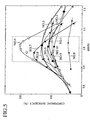
- Fig. 5 is a diagram showing relationships between geometrical configurations and the corresponding condensing efficiencies of the bulk-shaped lenses of the first embodiment of the present invention.
- Fig. 6 is a list showing the corresponding geometrical configurations in the bulk-shaped lens shown in Fig. 5, respectively.
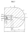
- Fig. 7 is a schematic cross-sectional view showing a light-emitting unit according to a modification of the first embodiment of the present invention.
- Figs. 8A to 8C show relationships between the protruding heights ⁇ implemented by the first lens surfaces and the corresponding beam intensity profiles, respectively.
- Figs. 9A to 9C show relationships between the protruding heights ⁇ implemented by the first lens surfaces and the corresponding beam intensity profiles, respectively.
- Figs. 10A to 10C show relationships between the protruding heights ⁇ implemented by the first lens surfaces and the corresponding beam intensity profiles, respectively.
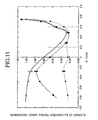
- Fig. 11 is a diagram showing relationships between the protruding heights ⁇ implemented by the first lens surfaces and the corresponding flatness of the illumination intensity profiles, respectively.
- Fig. 12 is a schematic cross-sectional view showing a light-emitting unit according to a second embodiment of the present invention.
- Fig. 13 is a schematic cross-sectional view showing a light-emitting unit according to a third embodiment of the present invention.
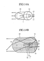
- Fig. 14A is a bird's-eye view showing a light-emitting unit according to a fourth embodiment of the present invention.
- Fig. 14B is a schematic cross-sectional view showing the light-emitting unit of the fourth embodiment of the present invention.
- Fig. 15 is a bird's-eye view showing a back mirror and a LED holder of the light-emitting unit of the fourth embodiment of the present invention.
- Fig. 16A is a bird's-eye view of a chart showing a light-emitting unit of a fifth embodiment of the present invention.
- Fig. 16B shows a schematic cross-sectional view of the light-emitting unit of the fifth embodiment of the present invention.
- Fig. 17A is a schematic cross-sectional view of the light-emitting unit of the fifth embodiment of the present invention, showing a detailed configuration in which a plurality of disk-shaped LEDs are disposed on a film-like substrate.
- Fig. 17B shows a top plan view corresponding to Fig. 17A.
- Fig. 18 is a figure showing circuit configuration in which plural disk-shaped LEDs are connected in series.
- Fig. 19 is a figure showing circuit configuration in which plural disk-shaped LEDs are connected in parallel.
- Fig. 20 shows a schematic cross-sectional view of the light-emitting unit according to a modification of the fifth embodiment of the present invention.
- Fig. 21 is a schematic cross-sectional view of the light-emitting unit according to a sixth embodiment of the present invention, showing a detailed configuration in which a plurality of bare-chips (LED chips) are disposed on a film-like substrate.
- LED chips bare-chips
- Fig. 22 is a schematic cross-sectional view of another light-emitting unit according to a modification of the sixth embodiment of the present invention, showing another mounting configuration in which a plurality of bare-chips (LED chips) are disposed on the film-like substrate..
- LED chips bare-chips
- Fig. 23 is a schematic cross-sectional view of the light-emitting unit according to a seventh embodiment of the present invention, showing a detailed configuration in which a plurality of bare-chips (LED chips) are vertically stacked on a film-like substrate.
- LED chips bare-chips
- Fig. 24 shows a schematic cross-sectional view, in which the LED chips shown in Fig. 23 are magnified.
- Fig. 25 shows a schematic cross-sectional view of a lighting equipment according to a eighth embodiment of the present invention.
- Fig. 26 is a bird's-eye view showing the configuration in which the lighting equipment of the eighth embodiment of the present invention is attached to a supporting substrate.
- Fig. 27 shows a schematic cross-sectional view of a light-emitting unit according to a ninth embodiment of the present invention.
- Fig. 28 shows a schematic cross-sectional view of a light-emitting unit according to a modification of the ninth embodiment of the present invention.
- Fig. 29 shows a schematic cross-sectional view of a light-emitting unit according to another modification of the ninth embodiment of the present invention.
- Fig. 30 shows a schematic cross-sectional view of a light-emitting unit according to a tenth embodiment of the present invention.
- Fig. 31 shows a schematic cross-sectional view of a light-emitting unit according to a eleventh embodiment of the present invention.
- Fig. 32A are bird's-eye views of a lighting equipment (display unit) according to a twelfth embodiment of the present invention.
- Fig. 32B shows a bird's-eye view of the display unit according to a modification of the twelfth embodiment of the present invention.
- Fig. 33 shows a schematic cross-sectional view of a light-emitting unit to be used in the display unit shown in Fig. 32B.
- Fig. 34A shows a schematic cross-sectional view of a light-emitting unit according to a thirteenth embodiment of the present invention.
- Fig. 34B shows a schematic cross-sectional view of an optical mixing device, in which the light-emitting units shown in the thirteenth embodiment of the present invention are merged.
- Fig. 35 shows a schematic cross-sectional view of a light-emitting unit according to a 14th embodiment of the present invention.
- Fig. 36A shows a partially broken bird's-eye view of a two-dimensional light-emitting unit according to a 15th embodiment of the present invention.
- Fig. 36B shows a bird's-eye view of the two-dimensional light-emitting unit, shown from a different orientation from the Fig. 36A.
- Fig. 37A shows a bird's-eye view of a two-dimensional light-emitting unit according to a 16th embodiment.
- Fig. 37B shows a bird's-eye view of a two-dimensional light-emitting unit according to a modification of the 16th embodiment
- Fig. 38 shows a bird's-eye view of a two-dimensional light-emitting unit according to a modification other than the 16th embodiment
- Fig. 39 shows a bird's-eye view of a two-dimensional light-emitting unit of another modification of the 16th embodiment of the present invention.
- Fig. 40A shows a partially broken bird's-eye view of a two-dimensional light-emitting unit according to a 17th embodiment
- Fig. 40B is a bird's-eye view showing a bulk-shaped lens to be used to the two-dimensional light-emitting unit shown in Fig. 40A.
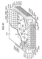
- Fig. 41 shows a partially broken bird's-eye view of a two-dimensional light-emitting unit according to a 18th embodiment
- Fig. 42 shows a partially broken bird's-eye view of a two-dimensional light-emitting unit according to a 19th embodiment
- Fig. 43 shows a partially broken bird's-eye view of a two-dimensional light-emitting unit according to a modification of the 19th embodiment
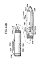
- Fig. 44A are schematic cross-sectional views of a hand-held instrument (portable lighting equipment) according to a 20th embodiment of the present invention
- Fig.44B is a partially broken bird's-eye view of the hand-held instrument shown in Fig. 44A, showing the disassembled state.
- Fig. 45 shows a magnified schematic cross-sectional view, showing the vicinity of LED chip in the hand-held instrument shown in Fig. 44A.
- Fig. 46A shows a schematic cross-sectional view of a hand-held instrument according to a modification of the 20th embodiment of the present invention.
- Fig. 46B shows a sectional view of a hand-held instrument according to another modification of the 20th embodiment of the present invention.
- Fig. 47 is a schematic view showing a locking/release system according to a 21st embodiment of the present invention.
- Fig. 48A is a sectional view of the locking/release system, showing a configuration in which a signal reception unit and a lock mechanism are merged in a desk, which serves as the locking object, the locking/release system is remote controlled by a parallel beam.
- Fig. 48B is a sectional view showing a configuration of a near-field operation, in which the signal reception unit and the lock mechanism are mutually approached.
- Fig. 49 is a schematic view showing a locking/release system having a security feature according to a 22nd embodiment of the present invention.
- Fig. 50 is a schematic cross-sectional view of a hand-held instrument (a hand tool having a lighting unit) according to a 23rd embodiment of the present invention.
- Fig. 51 is a schematic cross-sectional view showing a light-emitting unit according to a 24th embodiment of the present invention.
- Fig. 52 is a schematic cross-sectional view showing a light-emitting unit according to a 25th embodiment of the present invention.
- Fig. 53 is a schematic cross-sectional view showing a light-emitting unit according to a 26th embodiment of the present invention.
- Fig. 54 is a schematic cross-sectional view showing a photodetector according to a 27th embodiment of the present invention.
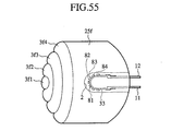
- Fig. 55 is a bird's-eye view showing a light-emitting unit of another embodiment of the present invention.
- Fig.1 is a schematic cross-sectional view showing a light-emitting unit of the first embodiment of the present invention.
- the light-emitting unit of the first embodiment of the present invention embraces at least a light source 1 emitting light having predetermined wavelength and a bulk-shaped lens 20 encapsulating nearly completely the light source 1.
- the bulk-shaped lens 20 encompasses a bulk shape (bullet-shape) lens body 4 identified by top surface 3, bottom surface and contour surface and a well-shaped concavity 6 implemented in the inside of lens body 4, dug to top surface 3 from the bottom surface.
- a ceiling surface of the concavity 6 implemented in the interior of lens body 4 serves as a first lens surface 2
- the top surface of the lens body serves as a second lens surface 3
- the inside of the concavity serves as a storing cavity 6 of the light source 1.
- the first lens surface 2 serves as an entrance surface 2 identified by the first curved surface.
- Storing cavity 6 encompasses a ceiling surface 2 identified by a first curved surface and a sidewall portion, which is configured to form the concavity in succession to the ceiling surface 2.
- the light incident from the entrance surface 2 outputs from the exit surface 3, or the second lens surface 3 identified by the second curved surface.
- the portion connecting the entrance surface 2 and the exit surface 3 of lens body 4 should be made of a transparent material to wavelength of light emitted from the light source, because the poption serves as an optical transmission medium.
- the light source 1 shown in Fig. 1 is a resin-molded LED encompassing a fist pin 11, a susceptor connected to the fist pin 11 so as to merge into a single body, an LED chip 13 mounted on the susceptor, molding resin 14 configured to encapsulate the LED chip 13, and a second pin 12 opposing to the first pin 11.
- a top surface of a main luminescence portion of this resin molded LED 1 has a convex-shaped curved surface as shown in Fig. 1. In this way, the light emitted from LED chip 13 is directed in predetermined divergence angle to right direction in Fig. 1, because the vicinity of the top surface of the resin mold 14 has the convex-shaped curved surface.
- a spacer of thickness around 0.25-0.5mm is interposed in order to fix the LED 1 and the bulk-shaped lens 20.
- the outside diameter 2r LED of the LED 1 is approximately same as the inside diameter 2r of the storing cavity 6, and the outside diameter 2r LED of the LED 1 is set slightly smaller than the inside diameter 2r. It is preferable that the spacer is disposed to exclude the main luminescence portion of the LED 1, or the left portion from the bottom face of LED chip 13 in Fig. 1.
- Bulk-shaped lens 20 has a almost cylinder geometry, similar to the geometry of the LED 1, apart from the top surface having the exit surface, identified by the convex-shaped second curved surface. Diameter (outside diameter) 2Ro of cylinder geometry portion of this bulk-shaped lens 20 is 10-30mm ⁇ .
- the diameter (the outside diameter) 2Ro of the bulk-shaped lens 20 can be chosen depending on purposes of use of the light-emitting units of the first embodiment of the present invention. Therefore, it can be less than 10mm ⁇ , and even more than 30mm ⁇ . However, in order to increase the condensing efficiency, it is preferable to satisfy the relationship: 10r > Ro > 3r Diameter (outside diameter) 2Ro of the bulk-shaped lens 20 can be more than 10 times of the inside diameter 2r of the storing cavity 6, and the large dimensional bulk-shaped lens of the present invention can operate similarly, but it is unfavorable for the purpose of miniaturization, because it becomes larger than requirement.
- the light appearing from region aside from a convex-shaped curved surface of the resin mold 14 of the LED 1 does not contribute to lightings, because it becomes so-called stray light component.
- the stray light component become possible to contribute significantly to lighting. That is to say, the inner wall portion 5 of the storing cavity 6 aside from the entrance surface (the ceiling surface) 2, identified by the first curved surface, can serve as the effective entrance surface of the light.
- components of light reflected back in each interface repeats multiple reflections between the storing cavity 6 of the LED 1 and the bulk-shaped lens 20 so that it become the stray light components.
- these stray light components cannot be extracted so as to contribute to effective lighting.
- these stray light components can finally contribute to lighting, because these stray light components are confined in the inside of the storing cavity 6, in the first embodiment of the present invention.
- the geometrical configuration being designed to satisfy Eq. (1), the light input from the inner wall portion 5 of the storing cavity 6 can be prevented from leaking from the contour surface of the bulk-shaped lens 20 again. Consequently, it becomes possible to extract the inherent light energy from the LED chip 13, with extraction efficiency approximately same as the internal quantum efficiency, without depending on geometry of the resin mold 14 nor the reflection component of the mutual optical system.
- Fig. 2A is schematic view showing a measurement system, in which the optical intensity profiles (the illumination intensity profiles) are measured vertically to optical axis, using the bulk-shaped lens 20 of the first embodiment of the present invention.
- a measuring distance (x) is measured along the optical axis direction.
- Fig. 2B shows the optics in which an earlier double convex lens is used, and similar measurement is done. In the measurement shown in Figs.
- an outside diameter of the bulk-shaped lens 20 of the first embodiment of the present invention is selected to be 30mm ⁇
- the outside diameter of the double convex lens 101 used in comparison is selected to be 63mm ⁇ , which is over two times of the bulk-shaped lens 20.
- Double convex lens 101 employed has a focal distance 190mm, which is disposed from the LED 1 in a location of 150mm along the x direction.
- Fig. 4 shows the intensity (illumination intensity) profile along y-direction similar to the data shown in Fig. 3, but the illumination intensity profiles are measured at various measuring distance x, and they are gathered up. Abscissa of Fig. 4 represents inverse-square of measuring distance x, that is to say of 1/x 2 , while ordinate represents maximum intensity (peak intensity) measured at respective measuring distance x. As shown in Fig. 4, data points are plotted perfectly on a line showing the inverse-square law, that is to say, on the line, which shows 1/x 2 , for the case of the bulk-shaped lens 20 according to the first embodiment of the present invention.
- Fig. 5 shows relationships between geometrical configurations of the bulk-shaped lens of the first embodiment of the present invention and corresponding condensing efficiency.
- the condensing efficiency is defined as the value: " Quantity of output light in divergence angle less than ⁇ 1 ° from the bulk-shaped lens " divided by "quantity of light in divergence angle less than ⁇ 15 ° from light source(LED) ". From the results shown in Fig.
- Fig. 6 is a list showing the geometrical configurations of respective bulk-shaped lenses shown in Fig.
- Fig. 7 is a schematic cross-sectional view showing a light-emitting unit related to a modification of the first embodiment of the present invention.
- Bulk-shaped lens 20 shown in Fig. 1 had the first concave-shaped lens surface and the second convex-shaped lens surface.
- the first and second lens surfaces can accept various kinds of topologies depending on purposes, and the protruding height ⁇ implemented by the first lens surface can take positive or negative value.
- ⁇ 0 can be employed.
- the positive direction of ⁇ is defined as the convex-shaped case, namely the positive direction corresponds to the topology of the first lens surfaces shown in Fig. 7.
- Figs. 8A-8C, Figs. 9A-9C and Figs. 10A-10C show the relationships between the protruding heights ⁇ of the convex portions defined in Fig. 7 and the beam intensity profiles, respectively.
- Outside diameter Ro of the cylinder geometry portion of the bulk-shaped lens 20 used for measurement is 15mm
- overall length L of the bulk-shaped lens is 25mm
- distance D between the first and second lens surfaces is 16mm
- inside radius r of the storing cavity 6 is 5.2mm
- refractive index n of a bulk-shaped lens is 1.54.
- Radius R of curvature of the second lens surface of this bulk-shaped lens is 8.25mm.
- a contour of resin molded LED 1 used for measurement is 5mm.
- FIG. 11 shows relationships between the flatness of the illumination intensity profiles and the protruding heights ⁇ of the convex portions, obtained by the results of Figs. 8A-8C, Figs. 9A-9 and Figs. 10A-10C in the irradiation areas defined by ⁇ 15cm at the measuring distance of 1m.
- the flatness of the illumination intensity is defined by: ((maximum) - (minimum)) / (mean value)
- a transparent material having the first refractive index n 1 such as epoxy resin, molds the LED 1 of the first embodiment of the present invention.
- the bulk-shaped lens 20 installs the LED 1 through air, having the second refractive index n 0 , which is different from the first refractive index n 1 .
- the LED 1 may be installed in the storing cavity 6 with fluid or liquid material aside from air.
- fluid Various kinds of "fluid” can be employed, if it is the gas or liquid, which is transparent to wavelength of light emitted from the LED 1.
- Spacer oil can be used between the LED 1 and the storing cavity 6 of the bulk-shaped lens 20.
- transparent materials of various kinds such as sol-like, colloid-like or gel-like materials can be employed.
- the bulk-shaped lens 20 has a third refractive index n 2 different from the second refractive index n 0 .
- the light from the LED chip 13 can be scattered or converged by choosing the first refractive index n 1 , the second refractive index n 0 and the third refractive index n 2 so that each has the optimum value.
- the optical path may be designed such that the third refractive index n 2 manifested by the optical transmission medium of the bulk-shaped lens 20 is gradually increasing or decreasing.
- the light-emitting unit of the first embodiment of the present invention desired light flux to required irradiation area is achieved, as the light beam contributing to lighting, without employing a large number of the resin molded LEDs 1, and desired illumination intensity can be easily obtained.
- This illumination intensity cannot be achieved by the optical system of the earlier known optical lenses.
- only single LED realized the illumination intensity implemented by the commercially available flashlight using the halogen lamp.
- the illumination intensity that cannot be predicted at all can be realized in the simple configuration as shown in Fig. 1.
- any LED of various kinds of color (wavelength) can be employed.
- white LED is preferred, because it is natural to a human eye.
- various kinds of configuration can be employed. For example, three pieces of LED chips including the red (R) green (G) and blue (B) chips can be stacked vertically so as to compose the white LED (cf. Fig. 24). In this case, from the resin mold 14, corresponding to the respective LED tips of different colors, totally six pins can be extracted.
- six pins may be merged into two pins, so as to assemble the LED in a configuration having two external pins.
- the number of the external pins become four, when one electrode (earth electrode) is elected to be common.
- the drive voltages of three pieces of LED chip, consisting of red (R) color, green (G) color and blue (B) color chips are controlled mutually independently, mixing of every color is possible, so that changes of tone of color can be enjoyed.
- transparent plastic materials such as acryl resin or various kinds of glass materials such as quartz glass, soda-lime glass, borosilicate glass, lead glass can be employed. Or crystalline materials such as ZnO, ZnS, SiC may be used.
- materials having pliability, flexibility and elasticity such as, for example, sol, gel, sol-gel mixture or transparence elastomer can be employed.
- it may be used in configurations such that sol, gel, sol-gel mixture are stored in container made of a transparent elastomer or a flexible transparent plastic material.
- transparent plastic materials such as, acryl resin is material to be preferable for mass-producing the large number of the bulk-shaped lens 20. That is to say, if die is made once, the large number of the bulk-shaped lenses 20 are molded simultaneously using this die, and the bulk-shaped lens 20 are easily mass produced.
- a light-emitting unit of the first embodiment of the present invention encompasses a main luminescence portion 8023 of light source, emitting light of predetermined wavelength, and a bulk-shaped lens 20 encapsulating nearly completely the main luminescence portion 8023 of light source.
- the bulk-shaped lens 20 encompasses a bulk-shaped lens body 4 having a top surface 3, bottom surface and a contour surface, and a well-shaped concavity 6 implemented in the inside of lens body 4, dug toward top surface 3 from the bottom surface.
- the main luminescence portion of light source is an edge of optical fiber bundle 8023, each fiber having a transmission portion made of a transparent material having the first refractive index.
- Optical fiber bundle 8023 shown in Fig. 12 merges plural optical fibers 8023a, 8023b, 8023c, ⁇ .
- Lights from plural optical fibers 8023a, 8023b, 8023c, ⁇ emit in predetermined divergence angle to right direction of Fig. 12.
- Configuration of respective plural optical fibers 8023a, 8023b, 8023c, ⁇ , composing optical fiber bundle 8023 may have straight geometry or twisting topology may be added to the straight geometry,.
- even a single optical fiber rather than optical fiber bundle 8023 can be employed, of course.
- contour of the optical fiber bundle 8023 may be a cylinder having a diameter (an outside diameter) 4-5 mm ⁇ .
- the side wall portion of the storing cavity 6 of the bulk-shaped lens 20 is implemented with a cylindrical geometry of diameter (inside diameter) 4.5-6mm ⁇ so that it can install the edge of optical fiber bundle 8023.
- a spacer of thickness around 0.25-0.5mm is interposed in order to fix the LED 1 and the optical fiber bundle.
- the bulk-shaped lens 20 has cylinder geometry, apart from the top surface serving as the exit surface 3, the top surface being identified by the convex-shaped second curved surface.
- Diameter of cylinder geometry portion of the optical fiber bundle is 10-30mm ⁇ .
- Diameter of the optical fiber bundle can be chosen depending on purposes of the light-emitting units of the second embodiment of the present invention. Therefore, it can be less than 10mm ⁇ , and even more than 30mm ⁇ .
- the optical fiber bundle 8023 of the second embodiment of the present invention embraces a plurality of optical fibers 8023a,8023b, 8023c ⁇ , each having clad layer with the first refractive index n 1 .
- the bulk-shaped lens 20 installs the edge of the optical fiber bundle 8023, through air having second refractive index n 0 , which is different from the first refractive index n 1 .
- the edge of the optical fiber bundle 8023 may be installed in the storing cavity 6 through a fluid or liquid material aside from air.
- the optical fiber bundle may have third refractive index n 6 different from the second refractive index n 0 .
- optical paths may be designed by setting the value of the third refractive index n 6 of the optical fiber bundle such that it is increasing or decreasing gradually.
- component of light reflected back in multiple reflections at each of interfaces between the edge of the optical fiber bundle 8023 and the storing cavity 6 of the optical fiber bundle becomes stray light component.
- these stray light components cannot be extracted such that it can contribute to lighting.
- these stray light components are confined in the inside of the storing cavity 6 in the second embodiment of the present invention, it becomes the components, which can contribute to lighting finally.
- Light source to input predetermined light to the other end portion of the optical fiber bundle 8023 of the second embodiment of the present invention is not always limited to the semiconductor light-emitting element. Because even if it is the light from an incandescent lamp, the edge of the optical fiber bundle 8023 installed in the inside of the storing cavity 6 of the optical fiber bundle can be held at low temperature. Therefore, if light source other than the semiconductor light-emitting element is used, because limiting of the light flux, prescribed by the output of LED, as in the light-emitting unit of the first embodiment of the present invention, can be removed, and an extremely bright lighting system can be realized.
- the geometry of the edge of the optical fiber bundle 8023 is not limited to the topology shown in the drawings, of course.
- Fig.13 is a schematic cross-sectional view showing a light-emitting unit of the third embodiment of the present invention.
- the light-emitting unit of the third embodiment of the present invention embraces at least composed a light source 1 emitting light of predetermined wavelength and a bulk-shaped lens 20 encapsulating the light source 1 by nearly completely.
- the bulk-shaped lens 20 encompasses a bulk-shaped lens body 4 identified by a top surface 3, a bottom surface and a contour surface and a well-shaped concavity 6 implemented in the inside of the lens body 4, dug toward the top surface 3 from the bottom surface.
- a ceiling surface of the concavity 6 serves as a first lens surface (an entrance surface) 2, a top surface of the lens body serves as a second lens surface (an exit surface) 3, inside of the concavity serves as a storing cavity 6 of the light source 1.
- iodine (I 2 )-tungsten lamp (halogen lamp) of diameter (outside diameter) 2-3mm ⁇ measured at the greatest portion, namely an incandescent lamp with a miniature lamp geometry can be employed.
- the cross sectional geometry of the bulk-shaped lens 20 is a bullet-shape as shown in Fig. 13.
- the concavity side wall 5 of the concavity 6 of the bulk-shaped lens 20 has a cylindrical geometry of diameter (inside diameter) 2.5-4mm ⁇ such that it can install the main luminescence portion of light source (an incandescent lamp) 1.
- a spacer of thickness around 1-2.5mm is interposed in order to fix the light source 1 and the bulk-shaped lens 20 (In Fig. 13, left side portion of the light source 1 corresponding to electrode-leads is called "socket part".)
- Diameter (outside diameter) of a cylinder shape portion of the bulk-shaped lens 20 of a bullet-shape can be chosen depending on purposes of the light-emitting unit of the third embodiment of the present invention. Therefore, it can be less than 10mm ⁇ , and even more than 30mm ⁇ .
- the bulk-shaped lens 20 of the third embodiment of the present invention has different refractive index n 1 from refractive index n 0 of air.
- concavity sidewall 5 of the concavity 6 aside from the entrance surface 2 (the ceiling surface) can serve as an entrance surface of effective light.
- Component of lights reflected back in each interfaces do multiple reflections between the concavity 6 of the light source 1 and the bulk-shaped lens 20 become stray light components.
- these stray light components cannot be extracted so as to contribute to lighting.
- these stray light components beings confined in the inside of the concavity 6 in the third embodiment of the present invention, they become the components which can contribute to lighting finally.
- the light source 1 is confined nearly completely in the concavity 6 of the bulk-shaped lens 20, including stray light components emitted from the light source 1, all output lights can effectively contribute to lighting.
- the light-emitting unit of the third embodiment of the present invention without needing large number of light source, desired light flux at irradiation area is obtained as light beam contributing to lighting, and desired illumination intensity can be easily achieved.
- This illumination intensity cannot be achieved by an optical system of the earlier known optical lenses.
- the illumination intensity which cannot be predicted at all by earlier technical common sense can be achieved in the simple configuration as shown in Fig. 13. As is apparent from the comparison between Fig. 2A and Fig.
- heat-resisting optical material when, as materials of the bulk-shaped lens 20 for the light-emitting unit of the third embodiment of the present invention, in view of the generation of heat by the light source (incandescent lamp) 1, a heat-resisting optical material is preferred.
- heat-resisting glass such as quartz glass, sapphire glass are preferable.
- heat-resisting optical materials of heat-resisting resins such as a polysulfone resin, a polyethersulfone resin, a polycarbonate resin, a polyeter ester amide resin, methacrylic resin, an amorphous polyolefin resin, polymeric materials having perfluoroalkyl radix can be employed. Even a crystalline material of SiC is preferable.
- weak heat-resisting resin such as acryl resin.
- a high-insulating sapphire substrate is used as epitaxial growth substrate of GaN, GaN is generally known as a material of blue LED. Because of this high-insulating sapphire substrate, the anode and cathode electrodes of Ga N blue LED are usually extracted together to the front face side of the Ga N epitaxial growth layer. Because this sapphire substrate is transparent to wavelength of blue LED, depending on the configurations of packages for the blue LEDs, luminescence from the blue LED can be extract from the rear surface direction of the substrate (Fig. 13, right direction). However, in the light-emitting unit of above mentioned embodiments of the present invention such as shown in Fig. 13, the configuration so as to take advantage of luminescence from the rear surface direction of substrate (the right direction) was not considered positively.
- a light-emitting unit of the fourth embodiment of the present invention embraces a semiconductor light-emitting element 1 and a bulk-shaped lens 25.
- this bulk-shaped lens 25 encompasses a bulk-shaped lens body 4 having a top surface 3, a bottom surface facing to the top surface and a contour surface and a well-shaped concavity 6 implemented in the inside of the lens body 4, the concavity 6 being dug toward the top surface 3 from the bottom surface.
- a ceiling surface of the concavity 6 arranged at an interior of the lens body 4 serves as a first lens surface (an entrance surface) 2, a top surface of a lens body serves as a second lens surface (an exit surface) 3, inside of the concavity serves as a storing cavity 6 of light source 1.
- a back mirror 31 is formed at bottom surface of the lens body 4.
- the back mirror 31 is extended to a part of the contour surface of bulk-shaped lens 25.
- the back mirror 31 covers a part of the contour surface of bulk-shaped lens 25, it may be possible to cover almost entire surface of the contour surface of the bulk-shaped lens 25.
- the back mirror 31 may be shaped by lathe / milling machine using metal such as Al, brass, stainless into geometry shown in Figs. 14A and 14B, or it may be molded by press working machines, and after that the face is polished. Furthermore, it is preferable that nickel (Ni) plating and gold (Au) plating are given to these surfaces, because reflectivity can be improved. As a low cost and simple manner, the configuration in which a high reflectivity metallic thin film such as Al thin film is bonded to the contour surface of the bulk-shaped lens can be employed. Or, the configuration in which thermoplastic is processed into the geometry shown in Figs.
- the metallic thin film having high reflectivity such as Al foil, or dielectric multilayer films is deposited on the surface by vacuum evaporation or sputtering, or even the configuration in which the high reflectivity polyester white film is adhesively bonded on the surface can be employed.
- configuration in which the high reflectivity metallic thin film or the dielectric multilayer films is directly deposited on the bottom surface of the bulk-shaped lens 25 by vacuum evaporation or sputtering, the configuration in which the high reflectivity metallic thin film is plated, or the configuration in which these composite films are deposited can implement the back mirror 31.
- thin film of various kinds of thickness of 50nm to 20 ⁇ m level can be employed as the back mirror 31.
- the semiconductor light-emitting element 1 shown in Figs. 14A and 4B is a molded LED 1, which embraces, a first pin 11, an LED chip 13 inserted in a hollow portion of a pedestal ring connected to the first pin 11, the LED chip 13 is fixed at the edge, a resin mold 14 encapsulating the LED chip 13, and a second pin 12 facing to the first pin 11.
- holes are opened so as to penetrate the first pin 11 and the second pin 12, configured such that the back mirror 31 does not cause the electrical short-circuit failure between the first pin 11 and the second pin 12.
- the LED chip 13 can execute the double sided luminescence oparatin, in which the luminescences are extracted from both front and rear surfaces of the LED chip 13 (in Figs. 14A and 14B, the luminescence from the rear surface emits to the right direction).
- a pedestal ring is not required to have the configuration in which the ring is completely closed, and even the ring having topology not closing, such as C-shape, U-shape, can be employed. The important thing is, any configuration, which can fix a part of the end surface of LED chip 13, can be employed.
- a top surface of this molded LED 1 has a convex-shaped curved surface as shown in Figs. 14A and 14B.
- the vicinity of the top surface of resin mold 14 has a convex-shaped curved surface in this way, and light outputting in the left direction (front side direction) from the LED chip 13 has directivity in predetermined divergence angle.
- light emitted to the right direction (the rear surface side direction) from the LED chip 13 is reflected back at the back mirror 31, and output from the front surface of LED chip 13 to the left direction.
- a predetermined divergence angle is given by a curved surface, or the convex-shaped top surface.
- the molded LED 1 is a cylinder configuration having diameter (outside diameter) 2-3mm ⁇ .
- a side wall portion of the concavity of bulk-shaped lens 25 is identified by a cylindrical geometry having diameter (inside diameter) 2.5-4mm ⁇ so that it can install the molded LED 1.
- the molded LED 1 is fixed to the LED holder 16, the head of the LED holder having a cup geometry, through the LED holder 16, the molded LED 1 and the bulk-shaped lens 25 are fixed each other.
- the LED holder 16 may be made of optically transparent material, having high electrical isolation property.
- wall thickness of the LED holder 16, at the part of the cup geometry located between the molded LED 1 and the concavity of the bulk-shaped lens 25 is around 0.25-0.5mm.
- the bulk-shaped lens 25 has almost similar cylinder configuration as that of the molded LED 1.
- Diameter (outside diameter) of cylinder geometry portion of the bulk-shaped lens 25 is 10-30mm ⁇ .
- Diameter (outside diameter) of the bulk-shaped lens 25 can be chosen depending on purposes of the light-emitting unit of the fourth embodiment of the present invention. Therefore, it can be less than 10mm ⁇ , and even more than 30mm ⁇ . But, it is preferable to choose the geometrical configuration of the bulk-shaped lens 20 such that it satisfies the already described Eqs. (1) - (3) or Eq. (6), of course.
- the LED holder 16 can be made into a single piece with the back mirror 31 as shown in Fig. 15, for example, and if the molded LED 1 is inserted in this back mirror built-in LED holder 16, the assembly process of the light-emitting unit of the fourth embodiment of the present invention can be simplified.
- the back mirror built-in LED holder 16 shown in Fig. 15 at the LED holder 16 disposed in a central portion, two through-holes for letting the first pin 11 and the second pin 12 go through are dug. The through-holes continue to the through-holes made in the above-mentioned back mirror 31. And by inserting the first pin 11 and the second pin 12 in these two through-holes, the molded LED 1 is fixed to the LED holder 16.
- the LED holder 16 can be made of transparent materials such as epoxy resin, having refractive index same as refractive index n 1 of the molded LED 1, or can be made of transparent materials having refractive index same as refractive index n 2 of the bulk-shaped lens 25. Or it may be made of transparent material having different refractive index from all of refractive index n 1 and refractive index n 2 . At all events, the LED holder 16 can be made of the optical material transparent to wavelength of light emitted from the molded LED 1. As the bulk-shaped lens 25, transparent plastic materials, glass materials, crystalline materials can be employed, and resin of colored or resin including luminescence material can also be employed.
- thermoplastics such as acryl resin or polyvinyl chloride resin are preferable materials for mass-producing the bulk-shaped lens 25. That is to say, die is made once, and if this die does extrusion or injection molding, the bulk-shaped lens 25 can easily implemented with mass production.
- stray light components In a general molded LED, light emitted from a place aside from the convex-shaped curved surface of resin mold 14 does not contribute to lighting, and it becomes so-called stray light components.
- the molded LED 1 is nearly completely confined in the concavity of the bulk-shaped lens 25, and because, in bottom surface of the bulk-shaped lens 25, the back mirror 31 is disposed, all these stray light components can be output from the top surface, serving as the luminescence surface, finally. Therefore, all stray light components contribute to lighting effectively.
- the inner wall portion 5 of the concavity aside from a ceiling surface serves as an entrance surface of effective light
- the stray light component which transmitted through the inner wall portion 5 is reflected back at the back mirror 31, and it can be output from the luminescence surface side finally.
- components of light reflected back at each interfaces repeat multiple reflections in various directions between the concavity of the molded LED 1 and the bulk-shaped lens 25, such that they become stray light components.
- these stray light components are confined in the inside of the concavity in the fourth embodiment of the present invention, and they are reflected back at the back mirror 31 in the inside, and are guided to the top surface side which serves as the luminescence surface. As a result, all these stray light components are output finally from the luminescence surface.
- desired light flux at irradiation area is achieved as light beam contributing to lighting, without requiring large number of the molded LED 1, so that desired illumination intensity can be easily obtained.
- This illumination intensity cannot be achieved by an optical system of the earlier known optical lenses. Therefore, the illumination intensity of the same level as achieved by commercially available slender body flashlight using halogen lamp can be realized with only single LED.
- the illumination intensity which cannot be predicted at all by earlier technical common sense can be realized by simple configuration as shown in Fig. 14A and 14B.
- Fig. 16A shows a schematic bird's eye view of a light-emitting unit of the fifth embodiment of the present invention
- Fig. 16B shows corresponding cross-sectional view.
- a light-emitting unit of fifth embodiment of the present invention embraces at least a plurality of diode chips 81,82,83,84, Vietnamese, each emitting light of predetermined wavelength, and a bulk-shaped lens 20 nearly completely installing the plurality of diode chips 81,82,83,84, « To be concrete, diodes chip 81,82,83,84, etc.
- the bulk-shaped lens 20 embraces a lens body made of transparent material to wavelength of light emitted from the plurality of diode chips, which is identified by an entrance surface 2, an exit surface 3 emitting the light incident from the entrance surface 2, the transparent material connecting the entrance surface 2 and the exit surface 3.
- the bulk-shaped lens 20 has geometry of a bullet-shape, identified by a contour surface of cylinder and a top surface of hemispheric.
- the bullet-shaped bulk-shaped lens 20 has a concavity, installing the disc-shaped LEDs 81,82,83,84,. « This concavity is identified by a entrance surface 2 and a sidewall portion formed in succession with the entrance surface 2. That is to say, the ceiling surface of the concavity serves as the entrance surface 2.
- the concavity is identified by a bullet-shaped geometry, defined by a cylinder-shaped contour surface and a hemispheric ceiling surface. Inside diameter of the cylinder defining the contour surface of the concavity may be around 2mm-6.5mm. On the other hand, outside diameter of the cylinder defining the contour surface of the bulk-shaped lens 20 can be chosen around 10mm-50mm.
- Difference between outside diameter2Ro of the cylinder defining the contour surface of the bulk-shaped lens 20 and inside diameter r of the cylinder defining the contour surface of the concavity, or the wall thickness can be chosen such as same level of the inside diameter r of the cylinder defining the contour surface of the concavity, or it can be chosen larger than around two to three times of the inside diameter r.
- the geometrical configuration of the bulk-shaped lens 20 should satisfy the already described Eqs. (1) - (3) or Eq. (6).
- the plural disc-shaped LEDs 81,82,83,84, Vietnamese are disposed on a film substrate 33, formed in a bullet-shape.
- a film substrate 33 formed in a bullet-shape.
- the plural disc-shaped LEDs 81,82,83,84, Vietnamese are disposed so as to contact with the entrance surface 2, because bright luminescence is obtained by the configuration.
- the film substrate 33 can be flexible organic materials.
- thin polyethylene terephthalate (PET) thin film or polyimide film having thickness of 25 ⁇ m-50 ⁇ m level can be employed as material of the film substrate 33.
- PET polyethylene terephthalate
- Al interconnections 221,222,223,224,225, ⁇ having thickness of 5 ⁇ m-15 ⁇ m level are delineated.
- Al interconnections 221,222,223, Vietnamese are delineated by etching method, after the Al thin film is deposited on the entire surface of the film substrate 33.
- the Al interconnections 221,222,223, Vietnamese may be delineated by screen printing method.
- aperture portions are formed in the Al interconnections 221 ,222,223, across
- the light-emitting unit of the fifth embodiment of the present invention desired light flux at the irradiation area, as light beam contributing to lighting, without requiring large number of disc-shaped LEDs 81,82,83,84, etc, is achieved, and desired illumination intensity can be easily obtained as well.
- This illumination intensity cannot be achieved by optical system of the earlier known optical lenses.
- plural disc-shaped LEDs 81,82,83,84, Vietnamese for the light-emitting unit of the fifth embodiment of the present invention various kinds of LEDs having various color (wavelength) can be employed. But, for lighting purpose such as for example a flashlight, the white LED is preferred, described in the first embodiment, because the white LED is natural to an eye of human.
- a glass material, a transparence plastic material, a crystalline material, which are described in the first embodiment, can be employed.
- transparent plastic materials such as acryl resin are preferable for materials for the bulk-shaped lens 20, because they are suited for mass production. That is to say, if die is made once, using this die, so as to ease the mass production, we can mold large number of the bulk-shaped lens 20.
- Plural disc-shaped LEDs 81,82,83,84,7-8 may be connected in series as shown in Fig. 18, or they may be connected in parallel as shown in Fig. 19.
- a current limiting circuit 812 and a drive circuit 811 are employed to be connected in series so that excess current is limited to flow into the plural disc-shaped LEDs 81,82,83,84, whil
- respective LEDs, or the D 1 , D 2 ,..., D n-1 , D n should be connected to corresponding current limiting resistors R 1 , R 2 ,...., R n-1 , R n in series, respectively, and the supply voltage is supplied through the drive circuit 811 to respective LEDs.
- a high-insulating sapphire substrate is used as an epitaxial growth substrate of gallium nitride (GaN) based semiconductor material. Because of this insulating substrate, the anode and cathode electrodes of the blue LED is usually extracted together from the front surface side of the epitaxial growth layer of the GaN based semiconductor material. Because this sapphire substrate is transparent to wavelength of blue LED, if design of predetermined optics such as using transparent material at the bottom surface of the disc type package, and mounting the blue LED on the transparent material, luminescence from blue LED can be extracted to the rear surface direction of the substrate. In this case, as shown in Fig. 20, it is preferable to arrange a back mirror 31 at bottom surface of the bulk-shaped lens 25. In Fig.
- Back mirror 31 covers almost entirely the contour surface of the bulk-shaped lens 25, only a part of the contour surface of the bulk-shaped lens 25 may be covered, or the formation on the contour surface may be omitted.
- Back mirror 31 may be formed by shaping the metal such as Al, brass, stainless using lathe / milling machine etc. to the geometry shown in Fig. 20, or molded by press working machines, and the surface is polished, afterwards. Furthermore, it is preferred, if nickel (Ni) plating and gold (Au) plating are given to the surface so as to improve reflectivity.
- the configuration in which metallic thin film of high reflectivity such as Al thin film is bonded to the surface can be employed.
- thermoplastic may be formed into the geometry shown in Fig.
- high reflectivity metallic thin film such as the Al foil or high reflectivity dielectric multilayer film may be deposited on the surface by vacuum evaporation or sputtering, or even the configuration in which high reflectivity polyester white film is adhesively bonded on the surface can be employed.
- the configuration in which the high reflectivity metallic thin film or dielectric multilayer film is directly deposited to the bottom surface of the bulk-shaped lens 25, by vacuum evaporation or sputtering, or the configuration in which composite films embracing these films are deposited on the surface can be employed.
- Plural disc-shaped LEDs 81,82,83,84, etc of Fig. 20 are mount on the film substrate 33, same as shown in Figs. 17A and 17B, and are connected to the first pin 11 and the second pin 12 by the Al interconnections.
- Fig. 20 although it is shown as if there is a gap between the entrance surface 2 identified by the ceiling surface of the concavity and the plural disc-shaped LEDs 81,82,83,84, Vietnamese it is preferable such that these plural disc-shaped LEDs 81,82,83,84, Vietnamese are contacted to the entrance surface 2, so as to obtain bright luminescence.
- the back mirror 31 Holes are formed at the back mirror 31 such that the first pin 11 and the second pin 12 can penetrate through the holes, because the configuration, in which the first pin 11 and the second pin 12 are not electrically short-circuited by the back mirror 31, is considered. If we made the film substrate 33, formed into the bullet-shaped, by transparent material, and the resin 14 filled in the inside of the bullet-shaped film substrate 33 is also made by the transparence material, luminescence from plural disc-shaped LEDs 81,82,83,84,7-8 propagates to the rear surface direction (in Fig. 20, to the right direction).
- the components which repeat the multiple reflections at each interfaces between the concavity of the bulk-shaped lens 25 and the plural disc-shaped LEDs 81,82,83,84, Vietnamese are confined in the inside of the concavity, and they are reflected back at the back mirror 31, they are led to the top surface serving as the luminescence surface. As a result, all these multiple reflection components are output finally from the luminescence surface.
- desired light flux at the irradiation area is obtained as the light beam contributing to lighting, without requiring extremely large number of disc-shaped LEDs 81,82,83,84, etc, and desired illumination intensity can be easily obtained as well.
- This illumination intensity is not achieved by the optical system of the earlier known optical lenses.
- the LED chip as shown in Fig. 21, encompasses an n-type semiconductor layer 402, an active layer 403, a p-type semiconductor layer 404 disposed on the sapphire (Al 2 O 3 ) substrate 401, through a buffer layer (the illustration is omitted).
- the sapphire (Al 2 O 3 ) substrate 401 is fixed to the film substrate 33 by adhesives 502.
- Anode electrode 405 can be disposed on the entire surface of the top face of the p-type semiconductor layer 404.
- the anode electrode 405 may be made of a transparent electrode layer to luminescence from the active layer 403.
- metallic oxide such as tin (Sn) doped indium oxide (ITO) and tin oxide (SnO 2 ) can be employed.
- metal layer may be formed into thinly enough so that it can serve as transparent electrode layer 405.
- Cathode electrode 406 serving as another electrode layer is not required, in particular, to be transparence.
- a bonding pad portion is arranged on a part of the anode electrode 405, and beam lead 512 made of copper (Cu) foil is connected to the bonding pad portion.
- Beam lead 511 made of the copper foil is connected to the cathode electrode 406 likewise.
- Beam leads 511,512 are connected to Al interconnections 221,222 through electrically conductive adhesives layer 501 respectively.
- LED chip may be assembled using solder balls 411,412 as shown in Fig. 22, in flip-chip configuration.
- the anode electrode 405 is connected to the Al interconnection 221 through the solder ball 411
- the cathode electrode 406 is connected to the Al interconnection 222 through solder ball 412.
- the film substrate 33 is made of transparent substrate, the light can propagate to two directions of front and rear surface directions. The light, which is emitted to rear surface direction reflects back at the back mirror 31 same as Fig. 20, and is returned to front surface direction.
- plural diode chips 81,82,83,84, Vietnamese are disposed on the surface of the film substrate 33, which is formed into the bullet-shape, or they are arranged, so to speak, in quasi-planar topology (quasi-two dimensionally).
- plural diode chips 61,62,63, Vietnamese are vertically stacked, as shown in Fig.
- Fig.24 shows in detail the stacked configuration embracing plural diode chips 61,62,63, whil Three levels of stacked layers are shown in the drawing for simplification, but multi-level structure more than four levels can be adopted, of course.
- the first level diode tip (the first level LED) 61 encompasses, an n type semiconductor layer 612, an active layer 613 and a p-type semiconductor layer 614 stacked on the sapphire substrate 611.
- the sapphire substrate 611 is fixed to a susceptor 64 by adhesives 602.
- An anode electrode 615 can be formed on the entire surface of the top face of the p-type semiconductor layer 614.
- a central portion of the anode electrode 615 may be made of a transparent electrode layer to the luminescence from the active layer 613.
- a frame-shaped peripheral portion of the anode electrode 615 is made of a relatively thick gold (Au) thin film having the thickness of 0.5 ⁇ m-2 ⁇ m level for bonding.
- Au gold
- a cathode electrode 616 is not required to be transparence, in particular.
- TAB lead (beam lead) 617 made of copper (Cu) foil is connected to the frame-shaped peripheral portion of the anode electrode 615.
- TAB lead (beam lead) 618 made of the copper foil is also connected to the cathode electrode 616.
- a second level diode chip (second level LED) 62 encompasses an n type semiconductor layer 622, an active layer 623 and a p-type semiconductor layer 624 stacked on the sapphire substrate 621.
- the sapphire substrate 621 is fixed on the first level diode tip 61 by transparent adhesives 605.
- An anode electrode 625 can be formed on the entire surface of the top face of the p-type semiconductor layer 624. A central portion of the anode electrode 625 may be made of a transparent electrode layer to the luminescence from the active layer 623.
- a frame-shaped peripheral portion of the anode electrode 625 is made of a relatively thick gold (Au) thin film having thickness of 0.5 ⁇ m-2 ⁇ m level for bonding.
- a cathode electrode 626 is not required to be transparent, in particular.
- TAB lead (beam lead) 627 made of copper (Cu) foil is connected to the frame-shaped peripheral portion of the anode electrode 625.
- TAB lead (beam lead) 628 made of copper foil is also connected to the cathode electrode 626.
- a third level diode chip (third level LED) 63 encompasses an type semiconductor layer 632, an active layer 633 and a p-type semiconductor layer 634 stacked on the sapphire substrate 631.
- the sapphire substrate 631 is fixed on the second level diode chip 62 by transparent adhesives 606.
- An anode electrode 635 can be formed on the almost entire surface of the top surface of the p-type semiconductor layer 634.
- a central portion of the anode electrode 635 can be made of a transparent electrode layer to luminescence from the active layer 633.
- a frame-shaped peripheral portion of the anode electrode 635 is made of relatively thick gold (Au) thin film of 0.5 ⁇ m-2 ⁇ m level for bonding.
- Au gold
- a cathode electrode 636 is not required to be transparence, in particular.
- TAB lead (beam lead) 637 made of copper (Cu) foil is connected to the frame-shaped peripheral portion of the anode electrode 635.
- TAB lead (beam lead) 638 made of copper foil is also connected to the cathode electrode.
- TAB leads (beam leads) 617,627,637,618,628,638 and bonding pads 615,625,635,616,626,636 we can use the techniques usually used as TAB bonding technique such as thermo compression bonding, ultrasonic bonding, gold (Au) bump joints, solder joints.
- TAB leads (beam leads) 617,627,637 are connected to a terminal 603 by electrically conductive adhesives or solders etc.
- TAB lead (beam lead) 618,628,638 are connected to terminal 604 by electrically conductive adhesives or solders etc.
- Resin seal 608 molds plural diode chips 61,62,63.
- the terminal 603 is connected to the second pin 12, and the terminal 604 is connected to the first pin 11.
- the terminal 603 and the terminal 604 are drawn to outside from the through holes formed in the back mirror 31 through a strengthening member 65. If the resin 14 filled in the concavity of the bulk-shaped lens 25 is made of transparent material to luminescence from plural diode chips 61,62,63, the lights can propagate to the rear surface direction (Fig. 23, right direction). Lights emitted from the plural diode chips 61,62,63 to the right direction (rear surface side direction) are reflected back at the back mirror 31, and are output to left direction from the front surfaces of plural diode chips 61,62,63.
- Plural diode chips 61,62,63, Vietnamese are not required to be the same LED chip. That is to say, as the plural diode chips 61,62,63, Vietnamese, various kinds and configurations can be employed. For example, as plural diode chips 61,62,63, if three pieces of LED chips including the red (R) green (G) and blue (B) chips are stacked vertically, as a whole, an output light of white can be achieved.
- red (R), green (G) and blue (B) chips as the red (R) LED chip, Al x Ga 1-x As, as the green (G) LED chip, Al x Ga y In 1-x-y P or GaP, and as blue (B) LED chip, In x Ga 1-x N or ZnSe can be employed.
- Al x Ga 1-x As, Al x Ga y In 1-x-y P, GaP do not require the sapphire substrate.
- ternary, quaternary, quinary, ??compound semiconductor mixed crystal are chosen as the materials for plural diode chips 61,62,63, Vietnamese, in which mole fractions may be changed.
- plural diode chips 61,62,63, Vietnamese made of In x Al y Ga 1-x-y N changing each of mole fractions, we can emit light in green (G)-blue (B) spectral range.
- an optical axis may disperse, first stack embracing vertically laminated plural diode chips, second stack embracing vertically laminated plural diode chips, and third stack embracing vertically laminated plural diode chips may be disposed on a bullet-shaped susceptor in the quasi-planar topology.
- a plurality of the light-emitting units explained one of the first to seventh embodiments can be arranged so as to provide a lighting equipment.
- a lighting equipment in this case, one-dimensional, two-dimensional or three-dimensional arrangement is possible.
- the light source of lighting equipment (lighting apparatus)
- an incandescent lamp, a small discharge tube, an electrodeless discharge lamp, a semiconductor light-emitting element can be adopted.
- the incandescent lamp may includes halogen lamps such as an iodine (I 2 )-tungsten lamp, a xenon (Xe)-tungsten lamp (xenon lamp), which may be called as “a Billiken lump”, a krypton (Kr)-tungsten lamp (krypton lamp), which is also called as “the Billiken lump”, and a miniature lamp with a vacuum evacuated tube or argon gas charged tube, the miniature lamp may be called “the nipple bulb” or "the spot bulb”. Furthermore, a miniature lamp such as a halogen miniature bulb is included in the incandescent lamp.
- halogen lamps such as an iodine (I 2 )-tungsten lamp, a xenon (Xe)-tungsten lamp (xenon lamp), which may be called as “a Billiken lump”, a krypton (Kr)-tungsten lamp (krypton lamp), which is also called as “the Billiken lump”, and a miniature lamp with
- the small discharge tube other than a fluorescence discharge tube, a small xenon lamp, a small metal halide lamp, a small size high-pressure sodium lamp, and a small size mercury lamp can be employed.
- the electrodeless discharge lamp the configuration in which the discharge media is charged in a bulb made of quartz glass, the discharge media including the noble gas such as argon (Ar), neon (Ne), xenon (Xe), krypton (Kr), with metal halide such as gallium (Ga), indium (In), thallium (Tl), and further mercury (Hg), zinc (Zn), sulfur (S), selenium (Se), tellurium (Te) can be employed.
- the noble gas such as argon (Ar), neon (Ne), xenon (Xe), krypton (Kr)
- metal halide such as gallium (Ga), indium (In), thallium (Tl), and further mercury (Hg), zinc (Zn), sulfur (S), se
- microwave of, for example, 100MHz-2.45GHz
- the discharge medium discharges, and it emits light.
- the microwave is preferable to be radiated from a transistor oscillating circuit.
- the semiconductor light-emitting element light emitting diode (LED) and a semiconductor laser can be employed.
- the semiconductor light-emitting element such as the LED has the characteristic of long life with low power consumption, but, in general, compared with the incandescent lamp such as the halogen lamp, the illumination intensity is low. Therefore, if a plurality (n pieces) of the semiconductor light-emitting elements D 1 , D 2 , Vietnamese,D n are combined together so that they can simultaneously emit, desired brightness can be achieved.
- a control circuit is preferable to encompasses a rectifier circuit rectifying commercial alternating current, a current limiting element (fixed resistor) connected to the rectifier circuit, a smoothing circuit connected to the current limiting element, and a constant current element (or a constant current circuit) connected to the smoothing circuit.
- a series circuit of n-pieces-semiconductor light-emitting elements D 1 , D 2 , Vietnamese,D n are shown, but the plural semiconductor light-emitting elements may be connected in parallel.
- a series connection of the semiconductor light-emitting elements (LEDs) of around 50 is preferable, because DC voltage of around 130V, which is obtained rectifying the commercial alternating current, can be just used, and the simplification of circuitry becomes easy.
- DC voltage of around 130V which is obtained rectifying the commercial alternating current
- the number of LEDs implementing the series connection can be chosen depending on the operating voltage.
- the lighting equipment embraces plural bullet-like bulk-shaped lenses 20a, 20b, Vietnamese,20f, Vietnamese disposed adjacently each other, plural light sources (LEDs) 1a,1b, Vietnamese,1f, Vietnamese, respective main luminescence portions of the light sources (LEDs) 1a,1b, Vietnamese,1f, etcare installed in the inside of well-shaped concavities implemented in the plural bulk-shaped lens 20a, 20b, Vietnamese,20 f, an optical-lens-fastening means (an optical-lens-fastening plate) 72 fixing plural bulk-shaped lens 20a, 20b, Vietnamese, 20 f, and a control circuit electrically connected respectively to the plural light sources (LEDs) 1a,1b, Vietnamese,1f, etc, the control circuit disposed in the vicinities of the optical-lens-fastening means 72.
- a configuration of each of plural bullet-like bulk-shaped lenses 20a, 20b, Vietnamese,20f « are shown in Fig 1.
- the control circuit is disposed on a circuit board 966, and is installed in the inside of a control circuit housing 965.
- this control circuit embraces a rectifier circuit, a current limiting element, a smoothing circuit, and a constant current element, etc.
- the circuit board 966 and the control circuit housing 965 are received in the inside of a cone-shaped isolation case 963.
- the optical-lens-fastening means 72 is fixed with fixing-metals 73a, 73b, Vietnamese to the isolation case 963.
- the circuit board 966 is fixed with fixing-metals 71a, 71b, etc.
- An AC-100V-electrode 961b is connected to the vicinity of the squeezed top portion of the cone-shaped isolation case 963 as shown in Fig 25.
- the AC-100V-electrode 961b is isolated by an isolation termination 962 from an AC-100V-electrode 961a.
- An AC-100V-mouthpiece 961 encompasses the AC-100V-electrodes 961a, 961b and the isolation termination 962.
- a power supplying lead 964a is connected to the AC-100V-electrode 961a, and a power supplying lead 964b is connected to the AC-100V-electrode 961b, and AC 100V are supplied to the control circuit installed in the inside of the control circuit housing 965 through the power supplying leads 964a, 964b.
- the LEDs serving as the light sources 1a, 1b, Vietnamese, 1 f, Vietnamese of the lighting equipment according to the eighth embodiment of the present invention (the lighting apparatus), can have configurations such as the bullet-shaped (the cannonball-shape) LED as shown in Fig 25, or the disc-shaped (the surface mount type) LED.
- the LEDs of various colors (wavelengths) can be employed.
- the white LED is preferable.
- plural LED chips can be disposed on the film substrate 33 formed as the bullet-shape as shown in Figs. 16A and 16B, and they may be installed in the storing cavity 6.
- the cluster of light sources 1a, 1b, Vietnamese LEDs, 1f, Vietnamese may include LEDs having different luminous colors.
- the lighting apparatus (the bulk-shaped lens cluster) shown in Fig. 25 is suitable for spotlighting equipment (lighting apparatus), by using separately, since it is superior in beam parallelism.
- spotlighting equipment light apparatus
- three spotlighting equipments emitting three colors of RGB, they can be used in horizont (cyclorama) illumination in a studio of a color TV broadcast.
- temperature rise in the studio can be suppressed, because the heat generation becomes low, by using LEDs as the light sources 1a, 1b, Vietnamese,1f, etc
- a large reduction of the power consumption is possible, or the reduction of electric power around 1/100 is achieved.
- the lighting apparatus is suitable for the studio of a high definition TV broadcast, by using the LEDs as the light sources 1a, 1b, owing, 1f, etc.
- the bulk-shaped lens cluster according to the eighth embodiment of the present invention may be attached to a supporting substrate 931 as shown in Fig 26. That is to say, if the bulk-shaped lens cluster shown in Fig 25 is attached to the supporting substrate 931 employing a socket pedestal 88, the lens cluster can be turned on/off by the information from a sensor 945. Because a mouthpiece 961 is attached to a cone-shaped isolation case 963 of the bulk-shaped lens cluster shown in Fig 25, if the bulk-shaped lens cluster is inserted in the lamp-socket mounted on the socket pedestal 88 disposed at the ceiling, which is identified as a supporting substrate 931, the lens cluster can be easily fixed to the supporting substrate 931.
- a circuitry portion 903 controlling lighting states of the bulk-shaped lens cluster shown in Fig 25 is disposed in a rear face of the supporting substrate 931. And the sensor 945 is connected to the circuitry portion 903. The sensor 945 supplies necessary information in order to control the lighting states of the bulk-shaped lens cluster.
- a circuit board 941 mounting the circuitry portion 903 for AC 100V control is attached.
- a light-emitting unit embraces a bulk-shaped lens 27 having at least a top surface serving as a luminescence surface, a bottom surface facing to the top surface and a lens body connecting the bottom surface to the top surface, the lens body having the first refractive index n 2 , a concavity formed from a part of the bottom surface to the top surface direction, in the inside of the lens body, and an optical path modification portion 35 with second refractive index n 0 different from the first refractive index n 2 formed inside of the lens body between the top surface and the concavity and a semiconductor light-emitting element 1 installed in the concavity.
- a transparent plastic material thermoplastic
- a glass material and a crystalline material etc.
- an optical path modification portion having the second refractive index n 0 a hollow space charged with air of refractive index n 0 as shown in Fig 27, or space filled with other solid material can serve.
- the optical path modification portion has the second different refractive index n 0 different from the first refractive index n 2 , because deflection occurs at interface between the portion having the first refractive index n 2 and the portion having the second refractive index n 0 , it is possible to change the propagation direction of the optical path.
- the optical path modification portion 35 having the second refractive index n 0 is provided in the inside of the lens body between the top surface and the concavity, the optical path modification portion 35 changes propagation direction of the light emitted from the semiconductor light-emitting element 1, incident from the ceiling surface of the concavity.
- optical path modification portion 35 designed to have the major axis along the central axis direction of the bulk-shaped lens 27 as shown in Fig 27, if the first refractive index n 2 is lager than the second refractive index n 0 , the luminous flux density around the central portion of the luminescence surface becomes low, and the lighting in which around the central portion of the optical axis is relatively dark is achieved. If, in the case of similar geometry of optical path modification portion 35, if the first refractive index n 2 is smaller than the second refractive index n 0 , the luminous flux density around the central portion of the luminescence surface increases, and the lighting in which around the central portion of the optical axis is relatively bright is enabled.
- a light-emitting unit according to the ninth embodiment of the present invention because it is basically similar to the light-emitting unit according to the first embodiment, the overlapped description is omitted.
- the geometry of optical path modification portion 36 designed to have the major axis perpendicular to the central axis direction of the bulk-shaped lens 28, the converse optical path modification occurs, when the optical path modification portion 36 is disposed between the top surface and the concavity in the inside of the lens body. That is to say, if the first refractive index n 2 is larger than the second refractive index n 0 , the luminous flux density around the central portion of the luminescence surface increases, and the lighting around the central portion of the optical axis is relatively bright is achieved.
- the luminous flux density around the central portion of the luminescence surface becomes low, and the lighting that around the central portion of the optical axis is relatively dark is achieved.
- Fig. 29 shows a schematic view showing a configuration of a light-emitting unit according to another modification of the ninth embodiment of the present invention, in which a back mirror 31 is disposed at a bottom surface of a bulk-shaped lens 29.
- a back mirror 31 is disposed at a bottom surface of a bulk-shaped lens 29.
- luminescence component from the rear surface of the LED chip 13 and stray light components are reflected back at back mirror 31, and they are led to the top surface side serving as a luminescence surface.
- all these stray light components are output finally from the luminescence surface, and extremely high conversion efficiency lighting is achieved, and the regulation of light intensity distribution at the irradiation surface becomes possible.
- cross-sectional shapes of the optical path modification portions 35,36,37 in the ninth embodiment of the present invention can have various geometries other than the double-convex geometry as shown in Figs. 27, 28 and 29, such as the plano-convex geometry or meniscus geometry.
- a light-emitting unit embraces a bulk-shaped lens (19a, 19b) having at least a top surface serving as a luminescence surface, a bottom surface facing to the top surface, a lens body connecting the bottom surface to the top surface, and a concavity formed from a part of the bottom surface to the top surface, the concavity is implemented in the inside of the lens body, a transmittance-changing means 41 disposed between the top surface and the concavity, the transmittance-changing means 41 disposed in the inside of the lens body, and a semiconductor light-emitting element 1 installed in the concavity.
- the transmittance-changing means 41 a mechanical shutter, an iris, or an electric transmittance-changing means such as a liquid crystal can be employed.
- the transmittance-changing means 41 is interposed between the front head portion 19a and the central portion 19b, depending on purposes, another configuration in which the transmittance-changing means 41 is embedded in a part of the bulk-shaped lens can be employed.
- the light-emitting unit according to the tenth embodiment of the present invention is, apart from the transmittance-changing means 41, basically similar to the light-emitting unit according to the first embodiment, and the overlapped description is omitted,
- the transmittance-changing means 41 by driving the transmittance-changing means 41 with mechanically or electrically, the optical intensity and beam diameter can be changed freely.
- the transmittance-changing means 41 the liquid crystal is employed, an active matrix implemented by thin film transistors (TFTs) may be disposed in the inside of the transmittance-changing means 41, and the each of the active matrix element may be driven with shift registers.
- TFTs thin film transistors
- a mechanical drive system such as micromotors will be disposed adjacent to the bulk-shaped lens (19a, 19b).
- the configuration in which the back mirror 31 is disposed at the bottom surface of the bulk-shaped lens 27 as shown in Fig 30, but, another configuration such that there is no back mirror, as for example Fig 1, can be employed, implementing the transmittance-changing means 41 in the lens body.
- a light-emitting unit embraces a bulk-shaped lens 30 encompassing having at least a top surface serving as a luminescence surface, a bottom surface facing to the top surface, a lens body connecting the bottom surface to the top surface, a concavity formed from a part of the bottom surface to the top surface direction, implemented in the inside of the lens body, and several scatterers 43 formed inside of the lens body between the top surface and the concavity, and a semiconductor light-emitting element 1 installed in the concavity.
- the scatterers 43 it is preferable to dope metal powders such as Al, Au, W, Ti, Mo into the bulk-shaped lens 30 made of transparence plastic material, a glass material etc., so that the metal powders coexist with the bulk-shaped lens 30. These metal powders will be mixed into the bulk-shaped lens 30, when the extrusion or the injection molding of the thermoplastic such as, for example, acryl resin or polyvinyl chloride resin is executed.
- the dimension of the scatterers 43 are selected such that they are larger than the wavelength of light, and various kinds of dimension are possible, which may include around micron order to several mm order, and any geometries can be adopted.
- the light-emitting unit of the first embodiment of the present invention is suited for the lighting equipment in the application fields in which relatively strong light beam with high directivity is required
- the light-emitting unit according to the eleventh embodiment makes the illumination intensity directivity weak, and is configured such that whole body of the light-emitting unit glitters, and it is suitable for the lighting equipment providing the beautiful sight.
- it may be used as an emergency light or bedside illumination equipment, or it may be used for decorating the interior of the room or the outdoors.
- a very bright lighting equipment and display unit can be implemented.
- one-dimensional, two-dimensional or three-dimensional arrangement of the light-emitting units may be possible.
- a traffic signal lamp can be implemented.
- red (R), green (G) and blue (B) double-sides-luminescence LED chips are stacked vertically on a transparent substrate , if each emission intensities of the red (R), green (G) and blue (B) LED chip is adjusted based on predetermined time schedule, red (R), yellow (Y) and green (G) can be displayed by the same lamp.
- Fig. 33 is cross-sectional view showing an example of the light-emitting unit, in which a groove is cut on a part of the top surface.
- a light-emitting unit related to twelfth embodiment of the present invention embraces a bulk-shaped lens 18 having at least a top surface serving as a luminescence surface, a bottom surface facing to the top surface, a lens body connecting the bottom surface to the top surface, a concavity formed from a part of the bottom surface to the top surface direction in the inside of the lens body, a groove 55 cut at a part of the top surface to the concavity direction in the lens body, and a semiconductor light-emitting element 1 installed in the concavity.
- the shape of the groove 55 is not limited to the V-shape as shown in Fig. 33, but various cross-sectional shapes such as U-shape and W-shape can be employed, and the direction and location of the groove can be changed depending on the contents of information to be displayed. By cases, a large groove eliminating all of the front surface (the top surface) of the bulk-shaped lens 18 can be included here. Except that the groove 55 is cut at the top surface of the bulk-shaped lens 18, it is basically similar to the light-emitting unit of the first embodiment, and the overlapped description is omitted.
- the geometry of the bulk-shaped lens of the present invention is not limited to the geometry of the bullet-shape analogy shown in Fig. 1, or the egg-shape (cocoon-shape) analogy shown in Fig. 14B, and it is possible to employ a configuration as shown in Fig. 34A, in which the diameter gradually becomes smaller approaching toward the tip portion.
- Fig. 34A By extending the bulk-shaped lens 17 into a long and thin topology as shown in Fig. 34A, the light flux is guided to the tip of the bulk-shaped lens 17, similar to the light propagation behavior observed in an optical fiber, and we can obtain a finely focused high intensity optical beam from the tip of the bulk-shaped lens 17.
- Fig. 34B we can merge the plural bulk-shaped lens 17a, 17b, 17c,.... into a single bulk-shaped lens 17z so as to implement an optical mixer. That is to say, if the plural lights from plural light sources, each installed in each of storing cavities 6a, 6b, 6c, are incident to respective entrance surfaces 2a, 2b, 2c, strong synthesized light can be emitted from the exit surface 3 of the bulk-shaped lens 17z.
- the top surface serving as the luminescence surface may embrace a first curved surface 7071 and a second curved surface 7072.
- a part of the optical path modification portion 36 of Fig. 28 has been forced out from the top surface of the bulk-shaped lens 28 so as to implement a top surface concavity 7073.
- luminous flux density around the central portion of the luminescence surface increases, the lighting around the central portion of the optical axis is relatively bright is achieved.
- a planar-light-emitting unit related to 15th embodiment of the present invention embraces at least a plurality of LEDs 2211,2212,2213, Vietnamese,2216,2221, Vietnamese,2226,2231, Vietnamese,2236 each emits a predetermined wavelength light, a plurality of bulk-shaped lenses 2111,2112,2113, Vietnamese,2116, 2121, Vietnamese,2126,2131, Vietnamese,2136, each installing a main luminescence portion of the respective LED and emitting light of the LED with a constant directivity, and a main reflector 2012 made of a plane mirror reflecting back the lights from the plural bulk-shaped lenses, a semitransparent plate 2011 transmitting the lights reflected back at the main reflector, the semitransparent plate is disposed in a configuration having a constant angle with the main reflector.
- planar-light-emitting unit related to the 15th embodiment of the present invention encompasses further a side reflector (the first side reflector) 2013 between the main reflector 2012 and the semitransparent plate 2011.
- another side reflector (the second side reflector) is facing to the side reflector 2013.
- Plural LEDs 2211,2212,2213, Vietnamese,2216,2221, Vietnamese,2226, 2231, ⁇ ,2236 are fixed each other by backplate 2015.
- a triangular prismatic cavity is formed by the main reflector 2012, the semitransparent plate 2011, the side reflector (the first side reflector) 2013, another side reflector (the second side reflector) and backplate 2015.
- the plural LEDs 2211,2212,2213, Vietnamese,2216,2221, Vietnamese,2226, 2231, Vietnamese,2236 are connected to LED socket, and predetermined voltages are applied to the LEDs.
- the bulk-shaped lens 2116 for the planar-light-emitting unit related to the 15th embodiment of the present invention is configured to nearly completely encapsulate the main luminescence portion of the LED.
- the concavity implemented in the bulk-shaped lens 2116 installing the main luminescence portion of LED 2216 has a ceiling surface identified as the first curved surface.
- the bulk-shaped lens 2116 embraces a top surface identified as the second curved surface emitting the light, facing the first curved surface.
- the main reflector 2012, the first and second side reflectors are configured such that they have polished surfaces of metals such as aluminum (Al), brass, stainless, and etc., and furthermore, nickel (Ni) film and/or gold (Au) film may be plated on the surfaces of them.
- metals such as aluminum (Al), brass, stainless, and etc.
- Ni nickel
- Au gold
- the configuration in which a high reflectivity metallic thin film such as Al foil or the high reflectivity polyester white film was bonded to the surface of resin substrate can be employed.
- an opalescent plate such as the resin plate in which white pulverized coal of high refractive index is dispersed in resin (to be concrete, such as the methacrylic resin opalescent plate is preferable).
- the semitransparent plate 2011 may be made of a rough surfaced opalescent plate, a rough surfaced transparent plate, or a molded resin sheet in the configuration embracing a transparent molding material and other light scattering corpuscles are kneaded to the transparent molding material.
- the semitransparent plate 2011 may be implemented by sticking a resin film on the surface, on a side or both sides of the resin film is delustered by a rough surface work.
- the semitransparent plate 2011 can accept colored or a transparent material depending on the luminous color of the LED.
- the bulk-shaped lens 2116 to be used in the planar-light-emitting unit related to the 15th embodiment of the present invention various kinds of glass materials, transparent plastic materials, crystalline materials explained in the first embodiment can be employed, and even a colored resin and resin including luminescence material can be accepted.
- transparent plastic materials such as acryl resin are preferable for mass production of the bulk-shaped lens 2116. That is to say, die is made once, and if the bulk-shaped lenses 2116 are molded by this die, they may be easily mass-produced.
- planar-light-emitting unit related to the 15th embodiment of the present invention without requiring large number LEDs, desired illumination intensity having uniformity over a large area is obtained.
- desired illumination intensity having uniformity over a large area is obtained.
- a slight change of fine gradation, such as the neutral tints, on the X-ray film can be easily observed. Or, worry of fatigue of eyes due to the flickering, or worry of the affect to human body from the fatigue of eyes can be eliminated.
- plural bulk-shaped lenses 2111,2112,2113, Vietnamese,2116, 2121, ??,2126,2131, ⁇ ,2136 are disposed in 3*6 matrix form, but, it is not necessary to limit to such matrix-form arrangement.
- the position of the first level plural bulk-shaped lens 2131, Vietnamese,2136 can shift from the position of the second level plural bulk-shaped lens 2121, Vietnamese,2126 by 1/2 pitch
- the position of the third level plural bulk-shaped lens 2111, Vietnamese,2116 can shift similarly from the second level plural bulk-shaped lens 2121, etc,2126 by 1/2 pitch so as to implement the close-packed arrangement.
- a planar-light-emitting unit related to the 16th embodiment of the present invention embraces at least an integrated lens 2031 having plural concavities and plural convex portions facing to the plural concavities, plural LEDs 2211,2212,2213, Vietnamese,2216,2221, Vietnamese,2226, 2231, etc,2236, installed in the plural concavities, each of LEDs emitting light of predetermined wavelength, a main reflector 2012 identified by a plane mirror reflecting back light from the plural convex portions (but the main reflector is not illustrated clearly, because it becoming the rear face side in bird's eye view of Fig.
- the planar-light-emitting unit related to the 16th embodiment of the present invention further embraces a side reflector (the first side reflector) 2013 arranged between the main reflector 2012 and the semitransparent plate 2011.
- a side reflector the first side reflector
- the illustration is omitted, as it becomes the rear face side of the bird's eye view shown in Fig. 37A, there is another side reflector (the second side reflector) facing to the side reflector 2013.
- the integrated lens 2031 is fixed to the backplate 2015.
- a triangular prismatic cavity is implemented similar to the configuration explained in the 15th embodiment.
- the plural LEDs 2211,2212,2213, Vietnamese,2216,2221, Vietnamese,2226, 2231, etc,2236 are connected to LED sockets, and supplied with predetermined voltage, respectively.
- the other configuration repeats the description in the 15th embodiment, and the overlapped description is omitted.
- the electric power is saved, and desired illumination intensity with uniformity over a large area can be easily got.
- desired illumination intensity with uniformity over a large area can be easily got.
- a slight change of fine gradation such as the neutral tints on the X-ray film can be easily observed.
- worry of fatigue of eyes is unnecessary, since there is no flickering.
- Fig. 37B is schematic bird's eye view showing a planar-light-emitting unit related to a modification of the 16th embodiment of the present invention.
- the outer circumferential surface of integrated lens 2031 shown in Fig. 37A has a waveform geometry having plural cylindrical surfaces
- the outer circumferential surface of the integrated lens 2032 shown in Fig. 37B is flat, different from the topology shown in Fig. 37A. Because other features are very similar to the planar-light-emitting unit related to the 16th embodiment of the present invention shown in Fig. 37A, the redundant description is omitted.
- Fig. 38 is a schematic bird's-eye view showing a planar-light-emitting unit related to another modification of the 16th embodiment of the present invention, and it shows an example of a planar-light-emitting unit having a large surface area, in which two units are assembled, preparing the integrated lens 2032 shown in Fig. 37B as a unit. That is to say, in Fig. 38, the first integrated lens 2032a and the second integrated lens 2032b are disposed adjacently.
- main reflector 2008 made of a plane mirror and a semitransparent plate 2016 transmitting the lights reflected back at main reflector 2008, between the main reflector 2008 and the semitransparent plate 2016 a constant angle is defined.
- the main reflector 2008 and semitransparent plate 2016 have areas two times larger than those of the main reflector 2012 and the semitransparent plate 2011 shown in Fig. 37B.
- Fig. 39 is a schematic bird's-eye view showing a planar-light-emitting unit related to a still another modification of the 16th embodiment of the present invention.
- the planar-light-emitting unit assembles four units, the configuration of each units is same as the integrated lens 2032 in Fig. 37B, so as to implement further large surface area than the configuration shown in Fig. 38. That is to say, in Fig. 39, under a adjacency assembled structure of the first integrated lens 2032a and the second integrated lens 2032b, another adjacency structure of the third integrated lens 2032c and the fourth integrated lens 2032d are disposed so as to form a layered structure. And, the planar-light-emitting unit shown in Fig.
- a main reflector 2009 identified by a plane mirror
- a semitransparent plate 2018 transmitting lights reflected back at the main reflector 2009, between the main reflector 2009 and the semitransparent plate 2018 a constant angle is defined.
- the area of the main reflector 2009 and the semitransparent plate 2018 can be designed to be four times lager than the main reflector 2012 and the semitransparent plate 2011 shown in Fig. 37B. However, if an appropriate angle is chosen, the area of the main reflector 2009 and the semitransparent plate 2018 are not required to be made four 4 times larger.
- a planar-light-emitting unit related to 17th embodiment of the present invention embraces at least plural LEDs 2211,...., emitting light of predetermined wavelength, plural bulk-shaped lenses 2311, 2312, 2313, 2321, 2322, 2331, 2332, 2333, each of bulk-shaped lenses emitting light from corresponding LED with a constant directivity and main luminescence portion of the LED is installed in the bulk-shaped lens, a main reflector 2012 identified by a plane mirror reflecting back lights from the plural bulk-shaped lenses and a semitransparent plate 2011 transmitting lights reflected back at the main reflector, between the main reflector and the semitransparent plate a constant angle is defined.
- Each of the plural bulk-shaped lenses 2311, 2312, 2313, 2321, 2322, 2331, 2332, 2333 has a compressed geometry spreading to horizontal directions, which is different from the bulk-shaped lens of the planar-light-emitting unit related to the 15th embodiment of the present invention.
- Plural bulk-shaped lenses 2311, 2312, 2313 are stacked on the plural bulk-shaped lenses 2321, 2322 shifting off 1/2 pitch, and furthermore, the plural bulk-shaped lenses 2321, 2322 are stacked on the plural bulk-shaped lenses 2331, 2332, 2333 shifting off 1/2 pitch, similarly (but may be optionally arranged in 3*3 matrix-form same as the 15th embodiment of the present invention, of course).
- planar-light-emitting unit related to the 17th embodiment of the present invention embraces further a side reflector (a first side reflector) 2013 between the main reflector 2012 and the semitransparent plate 2011.
- the planar-light-emitting unit embraces further another side reflector (a second side reflector) facing to the side reflector 2013.
- the plural LEDs 2211 Vietnamese are fixed to the backplate 2015.
- a triangular prismatic cavity is implemented by the main reflector 2012, the semitransparent plate 2011, the side reflector (the second side reflector extends), the backplate 2015, and another side reflector (the first side reflector) 2013.
- plural LEDs 2211, Vietnamese are connected to LED sockets so that they can be supplied with predetermined voltage.
- the compressed bulk-shaped lens 2311 related to the 17th embodiment of the present invention has major axis W and minor axis H. And, the compressed bulk-shaped lens 2311 encapsulates nearly completely the main luminescence portion of the LED 2211.
- the other plural compressed bulk-shaped lenses 2312, 2313, 2321, 2322, 2323, 2331, 2332, 2333 have similar geometries as shown in Fig. 40B.
- the compressed bulk-shaped lens 2311 encompasses a concavity installing a main luminescence portion of LED 2211, the concavity is aligned along the central axis of compressed bulk-shaped lens 2311, the concavity has a ceiling surface identified by a first curved surface, and the bulk-shaped lens is defined by a top surface identified by a second curved surface, emitting the light.
- the LED 2211 is a resin molded LED encompassing at least a first pin 11, a pedestal connected to the first pin 11, the pedestal merges with the first pin so as to form a single piece, a LED chip disposed on the pedestal, a resin mold encapsulating the LED chip, and a second pin 12 facing to the first pin 11. Because the resin molded LED 2211 is nearly completely confined in the concavity of the compressed bulk-shaped lens 2311, stray light components can contribute to lighting effectively.
- an inner wall portion of the concavity aside from the portion assigned as the entrance surface 2, identified by the first curved surface (the ceiling surface) can serve as the effective entrance surface of the light.
- Components of lights reflected back at each interfaces repeat multiple reflections in the concavity, between the LED 2211 and the concavity of the compressed bulk-shaped lens 2311, so as to generate stray light components. Because these stray light components beings confined in the inside of the concavity in the 17th embodiment of the present invention, the components can contribute to lighting finally.
- desired light flux at the irradiation area serving as the light beam contributing to lighting can be achieved, without requiring large number of the resin molded LEDs 2211, and desired illumination intensity having uniformity over a large area can be easily achieved.
- desired illumination intensity having uniformity over a large area can be easily achieved.
- a slight change of fine gradation, such as the neutral tints on the X-ray film can be easily observed.
- worry of fatigue of eyes is unnecessary, because the flickering is eliminated.
- planar-light-emitting units of a single directivity mode in which light is emitted to one direction
- bonding two planar-light-emitting units of the single directivity mode back to back can assemble a planar-light-emitting unit of the double directivity mode, in which lights are emitted to two mutually opposing directions.
- Fig. 41 is a diagram showing a planar-light-emitting unit of the 18th embodiment of the present invention, pertaining to other double directivity mode.
- the first integrated lens 2033a faces to the second integrated lens 2033b through a main reflector 2043 identified as a plane mirror.
- the main reflector 2043 is a double sided mirror, and is disposed between the first integrated lens 2033a and the second integrated lens 2033b diagonally.
- 18 pieces of concavities are cut in the first integrated lens 2033a so that 18 pieces of LEDs, the illustration of which is omitted, can be installed in the 18 pieces of concavities.
- first semitransparent plate 2041 disposed so as to define a constant angle with the main reflector 2043, transmitting the light reflected at the main reflector 2043, a second semitransparent plate 2042 disposed along the direction parallel to the first semitransparent plate 2041, the second semitransparent plate 2042 is aligned to the opposite side with regard to the main reflector 2043.
- the light reflected at the front surface of the main reflector 2043 propagate upward, and the lights reflected at the rear face of the main reflector 2043 propagate downward.
- Other features are similar to the planar-light-emitting unit related to the 16th embodiment of the present invention, and therefore the redundant description is omitted.
- the planar-light-emitting unit of the double directivity mode having desired illumination intensity with uniformity can be easily provided.
- the planar-light-emitting unit of the double directivity mode dissipates low power and achieves the double-sided lighting, without accompanied by flickering.
- Fig. 42 shows a planar-light-emitting unit of another single directivity mode according to 19th embodiment of the present invention.
- a first integrated lens 2034a faces to a second integrated lens 2034b through a ⁇ (lambda)-shaped main reflector.
- the lambda-shaped main reflector embraces a first reflector 2051 identified by a plane mirror and a second reflector 2052 identified by another plane mirror.
- the first main reflector 2051 is a plane mirror reflecting back the light from the first integrated lens 2034a mainly
- the second main reflector 2052 is another plane mirror reflecting back the light from the second integrated lens 2034b mainly.
- the planar-light-emitting unit related to the 19th embodiment of the present invention embraces further a semitransparent plate 2053 transmitting the lights reflected at the first main reflector 2051 and the second main reflector 2052, the semitransparent plate 2053 is configured to define constant angles with the first main reflector 2051 and the second main reflector 2052.
- a bottom plate 2054 is disposed in an opposite side with regard to the first main reflector 2051 and the second main reflector 2052l.
- a joint portion between the first main reflector 2051 and the second main reflector 2052, or a lambda-shaped top is separated from the semitransparent plate 2053 with distance d .
- the shade of the lambda-shaped top cannot be observed from the front surface of the semitransparent plate 2053. Because other features are similar to the planar-light-emitting unit explained in the 16th embodiment of the present invention, the redundant description is omitted.
- planar-light-emitting unit related to the 19th embodiment of the present invention a large area and longitudinally long size can be lighted up uniformly without requiring large number of LEDs.
- illumination intensity can be increased enough.
- the lighting of low power dissipation, which is not accompanied by flickering, is possible.
- Fig. 43 is schematic bird's eye view showing a planar-light-emitting unit related to a modification of the 19th embodiment of the present invention.
- an isosceles triangle serving as the third main reflector 2063 a plurality of bulk-shaped lenses 2611b, Vietnamese,2622b, 2711b, Vietnamese,2722b, 2811b, ....,2822b are stacked, and along the base of an isosceles triangle serving as the fourth main reflector 2064, a plurality of bulk-shaped lenses 2611a, Vietnamese,2622a, 2711a, Vietnamese,2722a, 2811a, Vietnamese,2822a are stacked.
- the bulk-shaped lenses 2622d, 2621d, 2620d, ??,2722d, ....,2822d and the bulk-shaped lenses 2611c, 2612c, 2613c, Vietnamese,2622c, 2711c, Vietnamese,2811c install LEDs, respectively, of course.
- the planar-light-emitting unit further embraces a semitransparent plate 2079 transmitting the lights reflected at the first main reflector 2061, the second main reflector 2062, the third main reflector 2063 and the fourth main reflector 2064 first main reflector 2061, the semitransparent plate 2079 is configured to define constant angles with the first main reflector 2061, the second main reflector 2062, the third main reflector 2063 and the fourth main reflector 2064.
- a bottom plate 2065 is disposed in direction parallel to the semitransparent plate 2079, and in the opposite side of the semitransparent plate 2079 with regard to the first main reflector 2061, the second main reflector 2062, the third main reflector 2063 and the fourth main reflector 2064.
- a top of the quadrangular pyramid is separated from the semitransparent plate 2079 with a constant distance d .
- the shade of the top of the quadrangular pyramid cannot be observed from the front surface of the semitransparent plate 2079.
- Other features are similar to the planar-light-emitting unit related to the 15th embodiment of the present invention, and the redundant description is omitted.
- the configuration in which four integrated lenses surround the circumference of the quadrangular pyramid, where the integrated lens is shown in Fig. 42 is possible.
- planar-light-emitting unit related to a modification of the 19th embodiment of the present invention as shown in Fig. 43, a comparatively thin planar-light-emitting unit having a large luminescence area can be provided. If the luminescence area of the planar-light-emitting unit becomes larger and larger, the effectiveness of reducing the number of LEDs becomes remarkable. That is to say, according to the planar-light-emitting unit related to the modification of the 19th embodiment of the present invention, comparing with earlier case in which the bulk-shaped lenses are not employed, number of LEDs employed become less than or equal to around 1/4 -1/10, and the reduction of number of LEDs by several hundred level is implemented, and therefore, unit price per area can be reduced.
- a battery case configured to apply predetermined voltage is prepared so as to install a battery (an AA size battery, for example), a slender flashlight of pen type (a portable lighting equipment) is implemented. And electrodes of LED 1 are connected to anode and cathode of the battery.
- the flashlight the portable lighting equipment
- the flashlights are superior in stability and reliability for a long term. In particular, because the power dissipation is low, the performance that life time of the battery is long can be achieved, which is not expected by earlier technologies.
- a hand-held instrument related to 20th embodiment of the present invention is a ballpoint pen, which embraces a visible light LED 1 serving as a semiconductor light-emitting element configured to output light of predetermined wavelength, the LED is mold by resin 14, and the light is emitted from the top surface of the resin 14, a power supply unit 3241,3242 configured to drive the semiconductor light-emitting element (visible light LED) 1, a bulk-shaped lens 20 having a top surface identified by a curved surface, configured to emit the light of semiconductor light-emitting element (visible light LED) 1, a concavity configured to install the resin 14, the concavity is implemented in the inside of the bulk-shaped lens, a holdings shank (a penholder) 3210 serving as a waveguide portion 3211 implementing a hollow space 3217 configured to install the bulk-shaped lens 20.
- a visible light LED 1 serving as a semiconductor light-emitting element configured to output light of predetermined wavelength
- the LED is mold by resin 14
- the light is emitted from the
- the waveguide portion 3211 has a cylindrical hollow space, and a central axis member (a ink cartridge) 3215 is installed in the hollow space.
- the hand-held instrument related to the 20th embodiment of the present invention embraces a power supply unit 3241,3242 driving the semiconductor light-emitting element (visible light LED) 1, and an electric switch portion 3226 controlling the power feeding from the power supply unit 3241,3242.
- a steel ball rotating freely, configured to supply appropriate ink to the surface of paper is arranged at a tip portion of the pen point (operation-tip) 3214 of the ballpoint pen.
- the steel ball any commercially available dimensions such as diameter of 0.2mm ⁇ -0.8mm ⁇ can be employed.
- the hand-held instruments can be disassembled into a writing body 3301 and a lighting body 3302 so that the lighting body 3302 can be independently used. That is to say, the hand-held instruments (the ballpoint pen) is configured such that the lighting body 3302 can be freely attached/released to/from the writing body 3301.
- the ink cartridge 3215 can be installed from the pen point portion at the right side to toward the left side in the cartridge installation cavity 3215A, which is arranged in the central axis member of the penholder 3210. In addition, when the ink cartridge 3215 must be changed after the ink becomes empty, the ink cartridge 3215 can be detached from the left side to the right side, through the cartridge installation cavity 3215A.
- a plastic material such as a comparatively lightweight transparent acryl resin, whose transmittance to the wavelength of the LED light is high, and by which the fabrication is easy, can be employed.
- the penholder 3210 can be formed such that it has diameter of 12mm and overall length of about 150mm.
- the coating layer 3212 is arranged mostly on the surface of the waveguide portion 3211, but the coating layer 3212 may be omitted by case. If we want to focus the light to the pen point portion, the coating layer 3212 should be used. Namely, in the case when the light from penholder 3210 is used as the spot lighting, the coating layer 3212 should be arranged. As the coating layer 3212 intended for the spot lighting, a high reflectivity metallic coating layer can be employed for protecting the surface of the waveguide portion 3211, and raising the transmission efficiency of the light in the waveguide portion 3211 at wavelength of the LED light.
- the coating layer 3212 to improve the fashionable nature, or the decorative nature, a skeleton type (semitransparent) colored resin coating layer of moderate transparency or an opaque colored resin coating layer can be employed.
- a skeleton type (semitransparent) colored resin coating layer of moderate transparency or an opaque colored resin coating layer can be employed.
- rubber coating layer and painted coating layer can be employed, if the optical transmittance of certain level can be manifested. For example, by using transmitted light from the coating layer 3212 effectively, it can be used as a penlight such as a security hand-held instrument for night walk or an amusement hand-held instrument in a concert meeting place.
- the optical dispersion portion 3219 can be implemented.
- a methodology configured to cut plural concavities having V-shaped, U-shaped, or splay-shaped geometry on the end of waveguide portion 3211, a methodology forming fine irregularities on the end of waveguide portion 3211, or methodologies fogging up the end of waveguide portion 3211 to the state of high frosted glass of comparatively high transparency can be employed.
- fine grains of transparent materials such as glass can be coated or bonded to the end of the waveguide portion 3211.
- a bulk-shaped lens engager 3217 serving as the hollow space configured to install the bulk-shaped lens 20 of the present invention.
- the bulk-shaped lens engager 3217 is, so to speak, a socket portion (female unit) configured to install the bulk-shaped lens 20.
- the bulk-shaped lens (plug portion: male unit) 20 of the lighting body 3302 is inserted in the bulk-shaped lens engager 3217 so as to be connected to the engager.
- a ceiling surface of the hollow space of the engager is identified by a concave surface having radius of curvature approximately same as the top surface of the bulk-shaped lens (plug portion: male unit) 20, and is configured such that the light from the bulk-shaped lens 20 is effectively guided to the waveguide portion 3211.
- inside diameter of the hollow space of the engager is set slightly lager than the outside diameter (a portion aside from the top surface) of the bulk-shaped lens (plug portion: male unit) 20, for example, around 0.05mm ⁇ 0.2mm lager.
- a female screw as a writing-body-engager 3218 is implemented (See the light-hand side in Fig. 44B.).
- a male screw serving as a lighting-body-engager 3228 configured to be coupled with the writing-body-engager 3218 of the writing body 3301.
- the writing body 3301 and lighting body 3302 are attached and /or detached using the male and female screws as an example here, other methodologies such as fitting methodology or clamping methodology can be employed.
- a reflecting mirror 3211A is mounted at the bottom plane of the cartridge installation cavity 3215A.
- the reflecting mirror 3211A is configured to increase the lighting efficiency of the light emitted from the visible light LED 1.
- the reflecting mirror can be disposed at the inner wall of the hollow space of the waveguide portion 3211 serving as the portion for installing the ink cartridge 3215, or at the external wall of the cartridge.
- minute irregularities serving as the irregular reflection plane are implemented at the inner wall of the hollow space, the interposed portion of the ink cartridge 3215 can be observed darkness, and we can expect the effectiveness such that the circumference of the writing body 3301 becomes slightly bright by the light from the irregular reflection planes. For using as a previously described penlight, it is effective to make an irregular reflection plane at the inner wall of the hollow space.
- the lighting body 3302 embraces a lighting-body-housing 3223, a semiconductor light-emitting element (visible light LED) 1 attached at the right side of the lighting-body-housing 3223 as shown in Fig. 44A and Fig. 44B, a power supply unit 3241,3242 installed at the central portion of the lighting-body-housing 3223, and an electric switch portion 3226 arranged at the leftmost edge of the lighting-body-housing 3223.
- a top surface of resin 14 is identified by the geometry of the top surface of commercial resin molded LED 1, and it is implemented by a concave geometry having predetermined radius of curvature.
- the resin molded LED 1 is identified by a cylinder configuration having, for example, diameter (outside diameter) of 2-3mm ⁇ .
- the bulk-shaped lens 20 has concavity configured to install the resin 14.
- a side wall portion of the concavity is implemented by a cylindrical geometry having diameter (inside diameter) of 2.5-4mm ⁇ so as to install the resin molded LED 1.
- a spacer or an adhesive having thickness of around 0.25-0.5mm is interposed between the LED 1 and the storing cavity 6 of the bulk-shaped lens 20. The spacer or the adhesive should be disposed at a location aside from the main luminescence portion of the LED 1.
- the bulk-shaped lens 20 has almost cylinder geometry same as the LED 1, apart from the top surface neighborhood serving as the convex-shaped exit surface 3.
- the diameter (outside diameter) of the cylinder geometry portion of the bulk-shaped lens 20 can be selected to a predetermined value smaller than the outside diameter of the lighting-body-housing 3223. For example, it may be chosen as 6 ⁇ 11mm ⁇ level.
- a top surface of the bulk-shaped lens 20 is identified by a concave geometry having predetermined radius of curvature, and the bulk-shaped lens 20 is configured to condense efficiently the light emitted from the visible light LED 1 and to emit the light outside.
- the lights emitted from a place aside from the convex-shaped curved surface serving as the top surface of the resin 14 become so-called stray light component, and do not contributed to the lighting.
- these stray light components can effectively contribute to the lighting. That is to say, the inner wall aside from the portion of the entrance surface (the ceiling surface) 2 of the concavity can serve as the effective entrance surface of the light.
- components of the light, reflected back at each interfaces, repeating the multiple reflections between the visible light LED 1 and the concavity become the stray light components.
- the illumination intensity is not achieved by the optical system of the earlier known optical lenses.
- illumination intensity of the same level as the commercially available flashlight with slender body, using halogen lamp can be realized only by a single LED.
- the illumination intensity which cannot be predicted by the earlier technical common sense can be achieved by the simple configuration as shown in Fig. 44A and Fig. 44B.
- the lighting-body-housing 3223 can be implemented by a pipe-shaped hollow cylinder body or other similar geometries, in which the power supply unit 3241,3242 can be installed.
- the lighting-body-housing 3223 can be made of materials such as stainless steel, aluminum alloy, or acryl resin or plastic materials. Similar to the penholder 3210, the lighting-body-housing 3223 can be made of, for example, transparent acryl resin or transparent plastic material, or it may be made of semitransparent/opaque acryl resin and semitransparent/opaque plastic material, which are colored moderately.
- the lighting-body-housing 3223 is implemented by the size which, for example, is equal to the outside diameter of the penholder 3210 of the writing body 3301.
- the LED chip 13 is mounted on a susceptor (a die pad) 202 arranged on a base pedestal (a stem) 15. And, the LED chip 13 is resin molded by the resin 14.
- the one end of the first lead interconnection 11 is connected to one electrode of the LED chip 13 (bottom electrode), through the susceptor 202, and another end is derived to the rear surface penetrating through the base pedestal 15.
- the one end of the second lead interconnection 12 is connected to the other electrode of the LED chip 13 (top electrode), and another end is derived to the rear surface penetrating through the base pedestal 15.
- the visible light LED 1 embraces the base pedestal 15, the susceptor 202, the LED chip 13, the first lead interconnection 11, the second lead interconnection 12, the resin 14 and etc.
- the base pedestal 15 may be made of insulating materials such as ceramics, encapsulated by metals such as stainless, brass or copper at the contour surface, or it may be made of same material as resin 14, merging to the resin 14,
- the step may be eliminated by the configuration in which the resin 14 and base pedestal 15 are implemented by the same outside diameter.
- LEDs of various colors can be employed.
- the white LED explained in the first embodiment is preferred; because the light from the white LED is natural to eyes of human.
- the resin 14 is implemented by a molded body, which provide the optical lens action and has the function to protect the LED chip 13 simultaneously.
- transparent thermosetting epoxy resin and transparent acryl resin can be used for the resin 14. Since the right side portion of resin 14 in Fig. 45 is identified by a concave geometry having predetermined radius of curvature, the resin 14 condense efficiently the light (white light) emitted from the LED chip 13 so as to shine the bulk-shaped lens 20.
- the power supply unit 3241,3242 can be implemented by two pieces of serially-connected batteries 3241 and 3242 such as AA size to AAAA size batteries so as to improve the portability of a hand-held instrument, while obtaining a moderate illumination intensity as well.
- disk type batteries such as a lithium ion battery or a manganese dioxide lithium battery can be employed, too.
- the power supply unit 3241,3242 is not limited to above -mentioned batteries, and can be implemented by other batteries such as small size rechargeable battery.
- the electric switch portion 3226 is basically implemented by a simple configuration such as a rotary or a push type switch (when a security feature, which will be explained in the 22nd embodiment, is required, a logic circuit, a pulse generator, a voltage regulator may be installed in the electric switches portion.).
- a voltage regulator which can independently control the drive the voltages of three pieces of LED chips of red (R), green (G) and blue (B) colors may be installed in the electric switch portion.
- One terminal of the electric switch portion 3226 is connected to the second lead interconnection 12 of the visible light LED 1 through the interconnection, which is not illustrated because it is arranged inward of the lighting-body-housing 3302.
- the other terminal of the electric switch portion 3226 is connected to the first lead interconnection 11 of the visible light LED 1 through an electrically conductive elastic member 3225, which holds the batteries 241 and 242 and also serves as the interconnection.
- an electrically conductive elastic member 3225 is made of metallic coil spring such as, for example, iron and copper.
- an electrically conductive elastic member 3225 may be implemented by a flat spring in which a metal plate is folded.
- a clip 3230 configured to carry the hand-held instrument storing in a pocket of a suit, for example, is attached.
- the hand-held instrument fitted with lighting portion can be stored in a pencil case, or in a pocket of a suit using the clip 3230 so as to carry. And, for example, in the case when we want to take notes under the slide screening in research meeting or lecture, or in the case when we want to take note on a notebook in night darkness, if we operate the electric switch portion 3226 of the hand-held instrument so that direct current is passed to the LED chip 13, identified by the visible light LED 1, from the power supply unit 3241,3242, visible light such as white light is emitted from the LED chip 13 as shown in Fig. 45. As shown by arrows in Fig.
- the visible light emitted from LED chip 13 is, at first, efficiently condensed by the resin 14, and is successively efficiently condensed by the bulk-shaped lens 20 and the waveguide portion 3211, respectively, and propagates to the direction of the pen point 3214, through the penholder 3210 via the waveguide portion 3211.
- visible lights emitted from the LED chip 13 visible light propagates to pen point 3214 along the shaft center of the writing body 3301 is reflected back at the reflecting mirror 3211A disposed at the bottom face of the cartridge installation cavity 3215A, and the visible light reflected back is reflected back again at the surface of bulk-shaped lens 20 and at the surface of resin 14, so that all of the visible lights can propagate toward the pen point 3214.
- the optical dispersion portion 3219 disperses the visible light transmitted through the waveguide portion 3211 finally, and necessary illumination intensity at the surface of paper, which is appropriate for the writing work in the dark, can be obtained.
- appropriate ink can be supplied to the surface of paper from ink cartridge 3215 depending on the rotation of the balls.
- the hand-held instrument since it encompasses the resin 14 efficiently condensing the light from the LED chip 13, the bulk-shaped lens 20 and the waveguide portion 3211 so as to improve the lighting efficiency, enough illumination intensity can be obtained, which is same level as obtained by incandescent lamp, in the practical use sense. Furthermore, the hand-held instruments manifests the low power consumption feature ascribable to the employment of the visible light LED 1, the lighting duration can be lengthened. For example, by comparing with the case when incandescent lamp is employed, the lighting duration longer than dozens of times to several hundred times can be achieved.
- the hand-held instrument is implemented by the simple configuration such that it encompasses only the resin 14, the bulk-shaped lens 20 and the waveguide portion 3211 each configured to condense the light from the visible light LED 1.
- the hand-held instrument is implemented by such simple configuration, fabrication is easy, and the fabrication cost can be reduced, too.
- the waveguide portion 3211 implements the penholder 3210, parts count employed in the writing body 3301 can be reduced. By the reduction of parts count, the hand-held instrument of further simpler configuration can be realized. As a result, furthermore, the hand-held instrument fitted with lighting portion having advantages such that fabrication is easy, and that the fabrication cost is low can be implemented as well.
- coloring is made on, at least either one of, the resin 14, the bulk-shaped lens 20, the waveguide portion 3211, the optical dispersion portion 3219, so as to emit light tinged with colors such as red, yellow, or purple rather than white light, so that notes can be taken in research meeting or lecture, in the illumination level that a person of periphery is not troubled, and further improving the decorative nature.
- a hand-held instrument (writing implement) shown in Fig. 46A (writing implements) is same as the configuration of the hand-held instruments shown in Fig. 44A to Fig. 45, it further embraces a outer cap 3231 configured to protect the pen point 3214 of the writing body 3301, which can be attached/detached to/from the penholder 3210 freely. And a clip 3232 is fitted on the outer cap 3231.
- a part of the outer cap 3231 in the vicinity of the pen point 3214 with a transparent material, and by choosing the geometry of the part of the vicinity of the pen point 3214 to a predetermined shape, it can serve as the flashlight, even in the state that the outer cap 3231 is attached.
- the writing body 3301 is identified as a fountain pen.
- the writing body 3301 embraces a pen point 3140 of the fountain pen, and an ink cartridge 3150 configured to supply ink to the pen point 3140.
- the writing body 3301 is identified as the fountain pen, the similar effectiveness achieved by the writing implements shown in Fig. 46A can be obtained.
- a locking/unlocking system configured such that an optical signal is transmitted from the hand-held instruments so that a locking object, such as an entrance, a gate, a door of each chambers, a door of a car, a drawer of a desk, a drawer or a door of a furniture, a lid of a seal box or an accessory box, is locked or unlocked is explained, employing the basic configuration of the hand-held instrument fitted with lighting portion related to the 20th embodiment of the present invention.
- the locking/unlocking system related to an embodiment of the 21st of the present invention embraces a signal-transmitting unit 3304 implemented by the hand-held instrument and a locking object having a signal-receiving unit 3305 configured to receive an optical signal from the signal-transmitting unit (the hand-held instrument) 3304.
- the hand-held instrument implementing the locking/unlocking system related to the 21st embodiment of the present invention encompasses a visible light LED 3340, molded by resin 14,the LED serving as a semiconductor light-emitting element outputting the optical signal from a top surface of the resin 14, a bulk-shaped lens 20 implementing a concavity configured to install the visible light LED 3340 in the inside and a waveguide portion 3211, serving as a penholder, having a hollow space configured to attach, install and detach the bulk-shaped lens.
- locking object encompasses the signal-receiving unit 3305 configured to receives the optical signal transmitted by the signal-transmitting unit (the hand-held instrument) 3304 and a locking mechanism 3306 configured to unlock in the case when it is determined that the received optical signal is identified as the predetermined signal. Furthermore, the locking object includes a drive power supply 3307 configured to supply power source to the signal-receiving unit 3305.
- the signal-transmitting unit 3304 has the same basic configuration as the lighting body 3302 explained in the hand-held instrument related to the 20th embodiment of the present invention, and it can be employed as the lighting equipment, it is configured to transmit the optical signal to the signal-receiving unit 3305 in the 21st embodiment. That is to say, the signal-transmitting unit 3304 transmits the optical signal to the signal-receiving unit 3305 so as to control the locking mechanism 3306, thereby implementing a transmitter configured to provide "an electronic key" for locking or unlocking of drawers of desks, etc.
- the signal-transmitting unit 3304 embraces a semiconductor light-emitting element (LED chip) 3410, a resin configured to condense the light (the optical signal) emitted from the LED chip 3410, a bulk-shaped lens 20, a power supply unit 3344 configured to supply voltages for driving the LED chip 3410, and an electric switch portion 3346 configured to control the power feeding from the power supply unit 3344.
- a semiconductor light-emitting element (LED) 3340 encompasses a LED chip 3410 and a resin configured to mold the LED chip.
- LEDs of various colors can be accepted, similar to the 20th embodiment of the present invention.
- the white LED described in the first embodiment is preferable.
- power supply circuits for respective colors are prepared in parallel, and independent control circuits are connected to the respective power supply circuits.
- the operating voltages of the green (G) and blue (B)-colored LEDs are higher than the red (R)-colored LED, is high.
- the balance of three colors of RGB may be adjusted by providing internal resistances.
- simultaneous parallel operations of three pieces of LED chips of RGB can be achieved by a common power supply unit 3344 and a common electric switch portion 3346 controlling the power feedings from the common power supply unit 3344, by adjusting the voltage with the respective internal resistances.
- 44A may encompass predetermined electronic circuits to implement the modulator (cf. the 22nd embodiment) such as a semiconductor memory of random access memory (RAM), a logic circuit, a pulse generator, a voltage regulator, instead of the simple configuration such as shown in the 20th embodiment.
- the modulator cf. the 22nd embodiment
- RAM random access memory
- logic circuit a logic circuit
- pulse generator a pulse generator
- voltage regulator a voltage regulator
- one end (top surface) of the signal-transmitting unit 3304 has a plug geometry so that it can be inserted in a socket shape portion implemented by the end of the writing body 3301, and so that it can attached/detached freely.
- a male screw may be implemented at a part of the plug geometry, and a female may be implemented at a part of the socket geometry.
- the waveguide portion 3211 implementing the penholder 3210 of the writing body 3301 has optical geometry such that it can efficiently condense the optical signal propagated through the bulk-shaped lens 20 having the plug geometry, and transmit to the tip direction, after condensing, the propagated optical signals are output through optical dispersion portion 3219 to outside finally.
- the locking mechanism 3306 judges the level of output current of the photodetector 3350, or judges the level of output voltage through a resistor, and judges whether predetermined input light is fed, using a comparator etc.
- locking mechanism 3306 conducts the unlocking actuating by predetermined drive mechanism.
- the locking mechanism 3306 maintains the locking state (the lockup condition) if the photodetector 3350 does not detect predetermined input light.
- using a predetermined timer it may be automatically locked after the unlocking actuation, or it may be configured such that the locking mechanism 3306 locks when the photodetector 3350 detected the predetermined input light again.
- the signal-receiving unit 3305 various kinds of photodetector 3350 can be adopted, but a semiconductor photodetector such as the photo diode is suitable for compactification, and it has a high sensitivity.
- a diode made of semiconductor material having a completely same specific optical energy (energy gap) as the semiconductor light-emitting element (LED) 3340 can be used. That is to say, the photodetection with highest sensitivity having wavelength-selectivity is achieved by making the specific optical energy of the light-emitting element equal to the specific optical energy of the photodetector.
- the photodetector (the photo diode) 3350 current flows when light having equal or larger energy than the specific optical energy of the photodetector is irradiated. In particular, extremely high sensitivity detection is achieved when light having exactly same energy as the specific optical energy of the photodetector is impinged, due to the wavelength resonance effect.
- a reverse biased LED having completely same configuration as the LED employed in the signal-transmitting unit, can be employed.
- an avalanche photo diode (APD) made of semiconductor material having completely same specific optical energy as the LED may be used.
- a phototransistor made of semiconductor material having completely same specific optical energy as the LED may be used.
- the locking mechanism 3306 actuates unlocking operation.
- the white light is adopted in the locking/unlocking system related to the 21st embodiment of the present invention, the transmission and reception of the signal will employ three colors of light, since it is known that white light is implemented by mixing of three colors of RGB lights. That is to say, since the white light can implement the signal transmission system of three channels, whish is strong against fluctuation and noise, photodetection by the signal-receiving unit 3305 can be done with extremely high sensitivity so as to actuate the locking/unlocking operations.
- the signal-receiving unit 3305 is installed in the entrance, the gate, and the door of each chamber. Therefore, in view of the spatial margin of the signal-receiving unit 3305, in order to condense the light from the LED 3340 from the signal-transmitting unit 3304, well known various optical systems such as earlier lenses can be adopted. In addition, if optical path reversibility is considered, the same optical system as the bulk-shaped lens employed in the writing implements 1, can condense the optical signal to the photodetector 3350.
- photodetectors other than the semiconductor photodetector such as photomultiplier tube
- photomultiplier tube it is preferable to add color filters corresponding to each of colors.
- the semiconductor photodetector by using semiconductor material having the specific optical energy completely same as the LED 3340 as previously described, the equivalent effectiveness as the configuration in which optical filters are built-in.
- Fig. 48A shows a remote control system using a collimated beam
- Fig. 48B shows an operative example of a near field operation corresponding to Fig. 47.
- a locking/unlocking system shown in Fig. 48A is implemented by a desk 3581 serving as the locking object, and embraces a signal-receiving unit 3305 disposed at neighborhood of the front plate 3585 of the drawer 3583, an electromagnetic solenoid 3560 serving as the locking mechanism 3306, a drive power supply 3307 configured to supply the driving current to the electromagnetic solenoid 3560.
- Locking hole 3582 configured to insert a shaft of the electromagnetic solenoid 3560 in the locked state is implemented in desk 3581.
- an optical-signal-receiving-hole (an optical key hole) 3584 penetrating to outward is arranged in the front plate 3585 of the drawer 3583.
- the optical-signal-receiving-hole 3584 may be implemented by a through-hole having a relatively small diameter compared with the thickness of front plate 3585. That is to say, it may be configured such that only a collimated beam is effectively arrive to the signal-receiving unit 3305 through the optical-signal-receiving-hole 3584.
- the optical signal emitted from the LED 3340 in the signal-transmitting unit 3304 is received by the signal-receiving unit 3305 through the optical-signal-receiving-hole 3584, and the driving current is supplied to the electromagnetic solenoid 3560 based on the optical signal received by the signal-receiving unit 3305 from the drive-power supply 3307.
- the shaft of the electromagnetic solenoid 3560 is descend by the driving current, the coupling between the locking hole 3582 and the shaft is broken so as to enable the unlocking actuating.
- the driving current raises the shaft of the electromagnetic solenoid 3560, it makes locking actuation by coupling the locking hole 3582 with the shaft.
- optical keyhole 3584 has a geometry of similar figure with the optical dispersion portion 3219 and is implemented by inside diameter slightly larger, for example, 0.1-0.3 mm, than the corresponding outside diameter of the optical dispersion portion 3219 so that it can install the optical dispersion portion 3219 of the tip of the writing body 3301.
- the light just arrives to the photodetector of signal-receiving unit 3305 in the state, which the optical dispersion portion 3219 is installed in the inside of the optical keyhole 3584. Even if the dispersion light is employed, by arranging the photodetector to the nearest-neighbor place of the optical dispersion portion, the effective optical intensity can be implemented.
- a push button may be implemented at a part of the inside diameter portion of the optical keyhole 3584. And, if it is configured such that when the tip of the writing body 3301 is interposed in the inside of the optical key hole 3584, the push button is pushed so that the power of the signal-receiving unit side become the ON-state, energy can be saved. In addition, protection of malfunctions due to the direct sunlight irradiation on the desk is possible.
- one-dimensional or two-dimensional image sensor as the photodetector of the signal-receiving unit 3305 shown in Fig. 48B, and if predetermined spatial pattern with encryption (coding) is formed on the surface of the optical dispersion portion 3219, it can be configured such that only when predetermined pattern of the specific hand-held instrument, corresponding to the specific person, is identified, the unlocking actuation is enabled. Furthermore, hologram color filter will be established at a part of waveguide portion 3211 or at a part of optical dispersion portion 3219, so that the signal-receiving unit 3305 can recognize the hologram pattern.
- the locking/unlocking system embracing the signal-receiving unit 3305, the locking mechanism 3306 and the drive-power supply 3307 is not limited to the example, in which it is implemented by the front plate 3585 of the drawer 3583 of the desk 3581, serving as the locking object, as shown in Figs. 48A and 48B, miscellaneous locking objects such as a drawer and a door of furniture, a lid of seal box or and accessory box, a door and a cover of a safe, can be adopted. Furthermore, a wall, a gate, a door of the entrance, a door of each chambers, a door of car, etc. can be employed as the locking object.
- the hand-held instrument fitted with lighting portion of the present invention can apply to the locking/unlocking system, improving a security feature.
- a security locking/unlocking system related to an embodiment of the 22nd of the present invention embraces a hand-held instrument serving as a signal-transmitting unit 3304 configured to transmit an optical signal and a locking object implementing a signal-receiving unit 3305 configured to receive the optical signal from the hand-held instrument (a signal-transmitting unit) 3304.
- the hand-held instrument related to the 22nd embodiment of the present invention encompasses, an LED 3340 molded by resin 14, serving as a semiconductor light-emitting element configured to output the optical signal from a top surface of the resin 14, modulator 3400 configured to generate an optical signal by modulating the light so as to include a predetermined personal identification information, a bulk-shaped lens 20 implementing a concavity configured to install the LED 3340 in the inside, and a waveguide portion 3211 serving as a penholder, implementing a hollow space configured to install the bulk-shaped lens 20, in such a way that the bulk-shaped lens is attached to or detached from the hollow space.
- the locking object related to the 22nd embodiment of the present invention encompasses a signal-receiving unit 3305 configured to receive the optical signal emitted from the hand-held instrument (signal-transmitting unit) 3304 and a locking mechanism 3306 configured to actuate unlocking, when the coincidence is confirmed after comparing the personal identification information contained in the received optical signal with the individual identification information registered in the locking object.
- the locking object encompasses a drive-power supply 3307 configured to supply the signal-receiving unit 3305 with a power source.
- the LED 3340 serving as the semiconductor light-emitting element embraces a first semiconductor light-emitting chip (LED chip) 3410 (R) configured to emit light of a first wavelength ⁇ 1 (red), a second semiconductor light-emitting chip (LED chip) 3410 (G) configured to emit light of a second wavelength ⁇ 2 (green) different from the first wavelength ⁇ 1 , a third semiconductor light-emitting chip (LED chip) 3410(B) configured to emit light of a third wavelength ⁇ 3 (blue) different from the first and second wavelengths ⁇ 1 , ⁇ 2 .
- LED chip semiconductor light-emitting chip
- the signal-receiving unit encompasses first, second and third photodetector 3051 (R), 3052 (G), 3053 (B) made of semiconductor materials having the same specific optical energies as the first, second and third semiconductor light-emitting chip 3410 (R), 3410 (G), 3410 (B), respectively.
- the locking mechanism 3306 encompasses a comparator 3631 to examine coincidence between the signal, generated from outputs of the first, second and third photodetector 3051 (R), 3052 (G), 3053 (B), and the registered personal identification information and a locking-driver 3640 configured to actuate unlocking, when coincidence between the signal and the registered personal identification information is confirmed.
- locking mechanism 3306 encompasses random access memory (RAM) 3632 configured to store the personal identification information.
- RAM random access memory
- the white LED encompassed three vertically stacked pieces of LED chips of red LED chip 3410 (R), green LED chip 3410 (G) and blue LED chip 3410 (B).
- modulator 3400 controls these three pieces of LED chips of red LED chip 3410 (R), green LED chip 3410 (G) and blue LED chip 3410 (B), independency.
- the modulator 3400 controls independently voltages of three pieces of LED chips of red LED chip 3410 (R), green LED chip 3410 (G) and a blue LED chip 3410 (B) respectively, so that relative intensities of respective colors are controlled, thereby desired color can be obtained by the mixing ratio.
- the modulator 3400 controls each of three pieces of LED chips. Therefore the modulator 3400 encompasses a digital-to-analog converter configured to control independently three circuits, using voltage from the power supply unit 3344 with signal of each 8 bit and a voltage regulator.
- the modulator 3400 not only controls the feeding of voltage from the power supply unit 3344, but also adjusts the pulse duration and repetition frequency, associated with source voltages applied to three pieces of LED chips of the red LED chip 3410 (R), green LED chip 3410 (G) and blue LED chip 3410 (B).
- the modulator 3400 can execute predetermined encoding of the source voltages with the binary coded signals.
- the modulator 3400 encompasses further a semiconductor memory such as RAM configured to store the 8 bit multiple-valued gradation data of respective colors or the binary coded signal.
- the electronic circuits including the semiconductor memory such as RAM, the logic circuit, the pulse generator and the voltage regulator, which are necessary for the modulator 3400 are monolithically integrated on a single chip as a semiconductor integrated circuit, and the semiconductor integrated circuit is installed in the electric switch portion 3226, as shown in Fig. 44A.
- a microprocessor may be merged in the semiconductor integrated circuits.
- the semiconductor integrated circuit controls independently the intensity of specific color, the pulse duration, the sequential order of the pulses, which are necessary for adding the security features, and further can store these information.
- a ten-key pad and other keyboards such as character-input-keyboards at somewhere of the configuration of the lighting body 3302 shown in Fig. 44A
- more complicated code signal and cryptogram can be input by the ten-key pad or the keyboard.
- the writing body 3301 is detached from the lighting body 3302, and by means of the pen point of writing body 3301, the keyboard can be operated.
- the keyboard may be implemented in the clip 3230 shown in Fig. 44A.
- the signal-receiving unit 3305 of the locking/unlocking system related to the 22nd embodiment of the present invention encompasses a semiconductor photodetector 3051(R) of red band, a semiconductor photodetector 3052 (G) of green band, and a semiconductor photodetector 3053 (B) of blue band, which are connected in parallel.
- these semiconductor photodetectors 3051 (R), 3052 (G), 3053 (B) we can use photo diodes 3051 (R), 3052 (G), 3053 (B), which are made of semiconductor materials having completely same specific optical energy as the red LED chip 3410 (R), green LED chip 3410 (G) and a blue LED chip 3410 (B).
- the photodetection of highest sensitivity with wavelength-selectivity is achieved. Because, in photodetectors (photo diodes) 3051 (R), 3052 (G), 3053 (B), current does not flow unless the light having energy equal to or more than energy gap is input, and when the light having energy same as the energy gap is input, by the wavelength resonance effect, extremely high sensitivity detection can be achieved.
- photo diodes 3051 (R), 3052 (G), 3053 (B) reverse biased LEDs having configuration exactly same as the red LED chip 3410 (R), green LED chip 3410 (G) and blue LED chip 3410 (B) can be employed.
- photodetectors 3051 (R), 3052 (G), 3053 (B) avalanche photo diodes made of semiconductor materials each having energy gap exactly same as the red, green, and blue LEDs can be employed.
- photodetectors 3051 (R), 3052 (G), 3053 (B) phototransistors made of semiconductor materials each having energy gap exactly same as the red LED chip 3410 (R), green LED chip 3410 (G) and blue LED chip 3410 (B) can be employed.
- by implementing the Darlington connection of the phototransistors further high sensitivity detection can be achieved.
- locking mechanism 3306 has level judgment circuits 3611,3612,3613, waveform shaping circuits (or, analog-to-digital converters) 3621,3622,3623. That is to say, at output sides of photodetectors 3051(R), 3052(G), 3053(B) of respective colors, level judgment circuits 3611,3612,3613 are connected respectively, and at the output sides of the level judgment circuits 3611,3612,3613, waveform shaping circuits (or, analog-to-digital converters) 3621,3622,3623 are connected.
- the waveform shapers 3621,3622,3623 feed binary or multiple valued outputs.
- the 8 bit multiple-valued gradation signals are fed, respectively.
- the comparator 3631 compares the 8 bit multiple-valued gradation data of respective colors stored in the RAM 3632 with outputs from the waveform shapers, and only when the coincidence is confirmed, the comparator 3631 drives the locking-driver 3640 so as to actuate unlocking. Or, when the comparator 3631 does not confirm the coincidence, the locking-driver 3640 maintains the locking state (lockup condition).
- the locking-driver 3640 can actuate locking when the comparator 3631 identified the coincidence between the 8 bit multiple-valued gradation data stored in the RAM 3632 and outputs of the photodetectors 3051 (R), 3052 (G), 3053 (B), after the photodetectors 3051 (R), 3052 (G), 3053 (B) detect predetermined input light again.
- the most simplest and effective technique is to move the timing of luminescence each other so as not overlap each other, by choosing the timing and the pulse duration of driving pulse of the LED such that the red LED chip 3410 (R), the green LED chip 3410 (G) and the blue LED chip 3410 (B) luminescence independently. In this way, by selection of the timing of luminescence, high sensitivity detection, using the wavelength resonance effect is enabled.
- a methodology finding the differentiation change of the outputs of photodetectors 3051 (R), 3052 (G), 3053 (B), while the timing is moved so as to overlap in order of red (R) color, green (G) color and blue (B) color can be employed.
- another methodology finding the differentiation change of the outputs of photodetectors 3051 (R), 3052 (G), 3053 (B), while the timing is moved so as to overlap in order of blue (B) color, green (G) color, red (R) color can be employed.
- the selection of the timing of luminescence can be provided in many ways. What is the simplest is to choose so that R, G, B luminescence independently in this sequence so that they don't overlap, respectively. In this case, they may be made to emit light sequentially according to the clock frequency, if a common clock frequency is selected between the signal-transmitting unit 3304 and the locking mechanism 3306. If the synchronous detection, opening the gates of photodetection by the clock frequency, the noise components and the influence of stray light can be eliminated in the locking mechanism 3306 side.
- the 8 bit multiple-valued gradation data stored in the RAM 3632 is compared with the integral value after the repetition of the predetermined cycle number in comparator 3631 so that the coincidence is confirmed.
- the "predetermined cycle number” may include even one cycle. The cycle number can be determined depending on the operating environment such that whether the direct sunlight is irradiated or not, or in view of the output power of the LED, the sensitivity of the semiconductor photodetector.
- the individual identification information (required information of the locking/unlocking system) can be generated.
- timings freely such that for person A, a sequence of RRBGBR, RRBGBR, RRBGBR, RRBGBR, for person B, a sequence of BRBRGG, BRBRGG, BRBRGG, and for person C, a sequence of GGGGBR, GGGGBR, GGGGBR, etc.
- codes of other plural personal identification informations can be aligned sequentially so as to emit light sequentially.
- the semiconductor memory such as RAM installed in the hand-held instrument can store all of the codes required for unlocking the keys of doors of these plural entrances, or the keys of doors of plural chambers.
- the locking mechanism 3306 can compare with the registered personal identification informations stored in the ROM installed in the locking mechanism 3306, and if coincidence is confirmed for one of the sequential luminescences, the specific locking object is unlocked, the trouble of looking for a specific key among a lot of keys becomes needless. In addition, it is not necessary to carry a lot of keys with.
- the pulse duration of the respective colors can be chosen so that it generates the personal identification information.
- pulse duration may be chosen based upon the clock frequency as a reference, if a common clock frequency for the signal-transmitting unit 3304 and locking mechanism 3306 is selected. That is to say, if the synchronous detection, opening the gate of photodetection triggered by the clock frequency, the noise component and the influence of stray light can be eliminated.
- the pulse duration may be chosen independently from the clock frequency under operating environment in which noise component and influence of stray light is low, of course.
- the various kinds of coding techniques used by normal information systems can be applied to respective colors (each channel), respectively, and further, they can be combined in all the colors.
- the locking/unlocking system related to the 22nd embodiment of the present invention shown in Fig. 49 shows example when it makes signal-transmitting unit 3304 corresponding to Fig. 48B and signal-receiving unit 3305 are mutually approached, but the locking/unlocking system is not limited to the example.
- the locking/unlocking system can be applied to a methodology irradiating the light to the signal-receiving unit 3305 located in a distant place by the condensed light with predetermined focal distance or by the collimated light, as shown in Fig. 48A, of course.
- the writing body 3301 is detached from the lighting body 3302 so as to expose the bulk-shaped lens 20 of the lighting body 3302, and the output light from the surface of the bulk-shaped lens 20 can be used.
- the optical intensity impinging the semiconductor photodetectors 3051 (R), 3052 (G), 3053 (B) may depend upon distance.
- the magnitude of optical intensity impinging the semiconductor photodetectors 3051 (R), 3052 (G), 3053 (B) is not detected as necessary information, but the relative intensity ratio of respective colors is detected, the reliability of necessary information will not be lost, even if the distance varies.
- the writing implements explained in the 20th embodiment is only a part of examples of the hand-held instruments of the present invention, and the 20th embodiment does not limit the present invention.
- a cosmetic instrument stick lipstick
- the configuration shown in Fig. 44A at the location of the ink cartridge 3215, if a solid material (lipstick) actuating push-out motion or torsional motion is disposed, a cosmetic instrument (stick lipstick) can be implemented.
- stick lipstick a cosmetic instrument
- the cosmetic instrument fitted with lighting portion of the present invention is convenient for adjusting makeup in darkness, in specific situation such as the case for cabin crew of aircraft.
- the cosmetic instrument fitted with lighting portion of the present invention can employ the white light, makeup of unaffected feeling just same as daytime can be achieved in darkness.
- the hand-held instrument of the present invention can be applied to miscellaneous hand tools such as the driver shown in Fig. 50 and a spanner or a wrench, which are omitted in the illustration.
- Driver shown in Fig. 50 can be attached/detached freely between the tool body 3311 and the lighting body 3302.
- a holdings shank (shank) 3210D serving as a waveguide portion 3211 implements a cylindrical hollow space configured to install a driver shaft (a central axis member) 3115 made of metal rod.
- the waveguide portion 3211 and the driver shaft 3115 are fixed rigidly each other by a shaft stopper 3116.
- tip of waveguide portion 3211 is identified by a convex shape so as to implement a light-condensing portion 3211 B, and configured such that the tip (head) of the driver shaft 3115 can receive an efficient local lighting in a working state.
- the tool body 3311 is detached from lighting body 3302 so that the tool body 3311 can be installed in the toolbox, while the lighting body 3302 is carried in a breast pocket, separately.
- the locking/unlocking of the tool box can be established by the output light from the surface of the bulk-shaped lens of the lighting body 3302, carried separately.
- the head of the lighting body 3302 is made large so that we can add force easily in Fig. 50.
- the lighting body 3302 can always be carried conveniently with a pocket of working clothes, for example.
- the bulk-shaped lens 20 implemented the storing cavity 6 identified by the concave-shaped first curved surface and embraced the exit surface 3 identified by the convex-shaped second curved surface.
- Fig. 1 is an example, and the first curved surface and the second curved surface can adopt miscellaneous topologies depending on purposes.
- Fig. 51 shows a bulk-shaped lens 21 defined by an exit surface 3, identified by a concave-shaped second curved surface, according to the 24th embodiment of the present invention.
- the concave-shaped second curved surface as shown in Fig. 51, because the light has tendency to disperse, homogeneity appropriate for backlight illumination (indirect lighting system) can be obtained.
- the curved surface can take miscellaneous topologies depending on purposes, and they may be modified into a bulk-shaped lens having the luminescence surface identified by the concave-shaped second curved surface. Applying the concave-shaped curved surface to the top surface (the luminescence surface), because the light has tendency to disperse, the homogeneity appropriate for the backlight illumination (indirect lighting system) can be obtained.
- the number of traffic accidents in Japan has tendency to increase year by year.
- the accident number related to bicycle holds about 3%.
- the accident by "non-lighting running" in the night stands out in the bicycle accidents.
- the mounting rate of bicycle lamps is nearly equal to 100%, the lighting rate is very low with 20%.
- battery type is desirable than the DC dynamo type for the bicycle lamp. What are required for the bicycle lamp are the enough brightness and the long lifetime of battery. Light source with low power dissipation is preferable in order to lengthen the lifetime of battery. In view of this aspect, the LED is preferable. However, generally, the illumination intensity from the LED is insufficient. In the 25th embodiment of the present invention, a light-emitting unit using the LED having enough brightness is explained.
- Fig. 52 is a schematic cross-sectional view showing the light-emitting unit according to the 25th embodiment of the present invention.
- the light-emitting unit related to the 25th embodiment of the present invention embraces at least a plurality of light sources (first to fourth light sources) 1a-1d configured to emits lights of predetermined wavelength, and a bulk-shaped lens 26 configured to encapsulate nearly completely respective main luminescence portions of the first to fourth light sources 1a-1d, installing independently and respectively.
- the bulk-shaped lens 26 implements a plurality of well-shaped concavities (the first to fourth concavities) 6a-6 d, separated each other and arranged in parallel.
- the respective well-shaped first to fourth concavities 6a-6d are defined by separate first to fourth entrance surfaces 2a-2d, and separate first to fourth concavity-sidewalls 5a-5d, formed successively to ceiling surfaces, the respective ceiling surfaces are identified by the first to fourth entrance surfaces 2a-2d.
- the exit surface 3 configured to emit plural lights incident from plural entrance surfaces 2a-2d is identified by a single curved surface.
- the lens body 4 connects between the first to fourth entrance surfaces 2a-2d and the single exit surface 3.
- the lens body 4 is made of a transparent material to wavelength of lights emitted from the light sources.
- each of the first to fourth light sources 1a-1d is a bullet-shaped LED having diameter (outside diameter) of 2-3 mm ⁇ at a maximum portion.
- the cross section of the bulk-shaped lens 26 has a geometry resembling a slice of kamaboko (boiled fish paste having a barrel vault geometry) having a constant thickness as shown in Fig. 52.
- the thickness between opposing two flat surface of the kamaboko should be more than three times of the outside diameter of respective first to fourth light sources 1a-1d.
- Each the first to fourth concavity-sidewalls 5a-5d of the first to fourth concavities 6a-6d implemented in the bulk-shaped lens 26, is identified by a cylindrical geometry (well shape geometry) of diameter (inside diameter) of 2.5-4mm ⁇ so as to install each of the main luminescence portions of the first to fourth light sources (bullet-shaped LED) 1a-1d. Spacers of thickness around 0.2-0.5mm are interposed between the first to fourth light sources 1a-1d and the first to fourth concavities 6a-6d, respectively, although the illustration is omitted, in order to fix the first to fourth light sources 1a-1d to the bulk-shaped lens 26.
- Width of the kamaboko -like bulk-shaped lens 26 can be chosen depending on purposes of the light-emitting unit related to the 25th embodiment of the present invention. Therefore, it can be less than 30mm, and even more than 100mm.
- Fig. 52 although four light sources 1a-1d are shown, they may be equal to or more then five, further they may be equal to or less than three. However, for bicycle lamp, the numbers around three to five are enough.
- Fig. 52 shows a configuration in which four light sources 1a-1d are arranged along one-dimensional direction, on a same plane level.
- the first to fourth back mirrors may be implemented to the first to fourth light sources 1a-1d, respectively.
- the pitch of disposition of the light sources 1a, 1b, 1c, Vietnamese should be chosen around three times of the outside diameter of light sources 1a, 1b, 1c, etc.
- outside thicknesses of the lens body 4 located at both ends of light sources are preferable to have a certain thickness of the level more than outside diameter of the light source. This condition almost satisfies Eq. (1).
- the white LED is preferred, because it is natural to human eyes as described in the first embodiment.
- the white LED may have configurations such that three pieces of LED chips of RGB are stacked vertically, or closely spaced each other in one package. That is to say, the first to fourth white LEDs having configurations such that three pieces of LED chips of RGB are encapsulated in the inside of the bullet-shaped resin seal, respectively, can be employed.
- the bicycle lamp may embrace a battery case and a battery (an AA size battery, for example) configured such that predetermined voltage can be supplied to the first to fourth white LEDs, respectively.
- the bicycle lamps embraces further an attachment configured such that the lamp body can be mounted on a bicycle handle.
- a bicycle lamp or the flashlight can be manufactured at low cost.
- the bicycle lamp or the flashlight has high stability and reliability for a long term, and in particular, the power dissipation is low, and the lifetime of battery is extremely long.
- first to fourth light sources 1a-1d and the first to fourth concavities 6a-6d of bulk-shaped lens 26 components of the lights reflected back at each interfaces, repeating the multiple reflections so as to become the stray light components.
- these stray light components cannot be extracted so as to contribute to the lighting.
- these stray light components become the components, which can contribute to lighting, finally, in the 25th embodiment of the present invention, because these stray light components are confined in the insides of the first to fourth concavities 6a-6d.
- the first to fourth light sources 1a-1d are nearly completely confined in the first to fourth concavities 6a-6d of the bulk-shaped lens 26, including the stray light components, all output lights emitted from the first to fourth light sources 1a-1d, can contribute to lighting effectively.
- desired illumination intensity can be easily obtained, by establishing light flux having desired parallelism, which is enough for the bicycle lamp.
- the illumination intensities cannot be achieved by the optical system of the earlier known optical lenses.
- the illumination intensity that cannot be predicted at all by the earlier technical common sense can be realized in the simple configuration, as shown in a Fig. 52.
- the materials for the bulk-shaped lens 26 to be use in the light-emitting unit related to the 25th embodiment of the present invention transparent plastic materials, glass materials, crystalline materials, described in the first embodiment, can be employed. Further, colored resin or resin including luminescence material can be employed. Among them, thermoplastics such as acryl resin or polyvinyl chloride resin are materials preferable to mass production of bulk-shaped lens 26.
- other light sources such as incandescent lamps including halogen lamp, small discharge tubes, and electrodeless discharge lamps can be employed instead of LEDs.
- heat-resisting optical materials are preferable for the bulk-shaped lens 26.
- heat-resisting optical materials heat-resisting glasses such as quartz glass, sapphire glass are preferable.
- heat-resisting optical materials such as the heat-resisting resin of polycarbonate resin can be employed. Even crystalline materials such as ZnO, ZnS, SiC can be employed.
- a lightness sensor to the bicycle lamp so that the bicycle lamp can automatically turn on, when it became dark.
- the LED may illuminate in the unmanned condition, because it dissipates low power.
- it can be so configured that bicycle lamp turns on only in driving, by providing a weighting sensor to a saddle strap and/or pedals.
- a logical product (AND) circuitry configured to input the signal from the lightness sensor and the signal from the weighting sensor, it can be configured such that it turns on automatically only both condition of driving and dark are satisfied, and it turns off the light automatically when the signal from the weighting sensor disappeared.
- the technical advantages in which the modification of optical path such as divergence and convergence of lights, and the modification of focal point are possible and easy are shown, without modifying the configuration of light source (LED) itself, by using the bulk-shaped lens 20.
- the light beam diameter from the resin molded LED 1 can be spread by the configuration as shown in Fig. 53, in which a second bulk-shaped lens 23 is arranged outside of a first bulk-shaped lens 20, and a third bulk-shaped lens 24 is arranged outside of the second bulk-shaped lens 23.
- the second bulk-shaped lens 23 has a second storing cavity configured to install the first bulk-shaped lens 20, and made of transparent material to wavelength of light, similar to the first bulk-shaped lens 20.
- a ceiling surface of the second storing cavity serves as an entrance surface (a third curved surface), a fourth curved surface facing to the third curved surface serves as an exit surface.
- the third bulk-shaped lens 24 implements a third storing cavity configured to install the second bulk-shaped lens 23.
- a ceiling surface of the third storing cavity serves as an entrance surface (a fifth curved surface), a sixth curved surface facing to the fifth curved surface serves as an exit surface.
- the LED 1 is molded by transparent material 14 such as epoxy resin having first refractive index n 1 in the 26th embodiment of the present invention.
- the first bulk-shaped lens 20 having third refractive index n 2 installs the LED 1 through air having the second refractive index n 0 .
- the second bulk-shaped lens 23 having fourth refractive index n 3 installs the first bulk-shaped lens 20 through air having the second refractive index n 0 .
- the third bulk-shaped lens 24 having the refractive index n 4 installs the second bulk-shaped lens 23 through air.
- the LED 1, the first bulk-shaped lens 20 and the second bulk-shaped lens 23 may be installed in respective storing cavities through a fluid or liquid material aside from air.
- the optical path may be designed such that the refractive indexes increase from the third refractive index n 2 , through the fourth refractive index n 3 to the fifth refractive index n 4 , or it may decrease gradually from the third to fifth refractive index.
- the beam diameter is widened too much, like the 26th embodiment of present invention, illumination intensity decreases. Therefore, it becomes improper for the purpose such as a flashlight.
- the backlight illumination in which uniform lighting is required. That is to say, luminescence point of the LEDs shine like spots when a plurality of normal bare LEDs are employed in the backlight illumination (the indirect lighting system), and variations of brightness becomes significant.
- the beam diameter is magnified to 50-100mm ⁇ level as shown in Fig. 53, the uniform backlight illumination is achieved.
- a second bulk-shaped lens can be disposed outside of the bulk-shaped lens (the first bulk-shaped lens) 25 that having the back mirror 31 explained in the fourth embodiment, and furthermore, a third bulk-shaped lens may be arrange outside of the second bulk-shaped lens.
- a light beam diameter of molded LED 1 can be magnified for a purpose of obtaining a further larger irradiation area.
- the second bulk-shaped lens is made of transparent material to wavelength of light, and implements a concavity configured to install the first bulk-shaped lens 25 and a luminescence surface identified by a curved surface.
- the third bulk-shaped lens will implement a concavity configured to install the second bulk-shaped lens.
- Fig. 54 is a schematic cross-sectional view showing a light-receiving unit related to the 27th embodiment of the present invention.
- the light-receiving unit related to the 27th embodiment of the present invention embraces a photodiode (a photodetector) such as a pin photodiode or an avalanche photodiode configured to detect light of predetermined wavelength and a bulk-shaped lens 20 configured to encapsulate nearly completely the photodiode.
- the bulk-shaped lens 20 has an entrance surface (the second lens surface) 3 identified by a second curved surface.
- a concavity 6 configured to install the receiving portion of the photodetector (a photodiode) is implemented.
- a ceiling surface of the concavity is identified by a first curved surface.
- the light incident from the entrance surface (the second lens surface) 3 emits from the ceiling surface of the concavity serving as the exit surface (the first lens surface) 2.
- And light from the exit surface (the first lens surface) 2 is condensed to the receiving portion of the photodetector so as to incident on the photodetector.
- the photodetector shown in Fig. 54 encompasses at least a first pin 11, a pedestal connected to the first pin 11 so as to merge into single piece, a photodiode chip 9 disposed on the pedestal, and second twin pin 12 facing to the first pin 11.
- the side wall portion of the storing cavity 6 of the bulk-shaped lens 20 is identified by a cylindrical geometry having diameter (inside diameter) 2.5-4mm ⁇ so that it can install the photodetector. Although the illustration is omitted, a spacer of thickness around 0.25-0.5mm is interposed between the photodetector and the storing cavity 6 of the bulk-shaped lens 20, in order to fix the photodetector to the bulk-shaped lens 20. The spacer is disposed at place aside from the main receiving portion of the photodetector, or the left side than the bottom face of photodiode chip 9, in Fig. 54.
- the bulk-shaped lens 20 is implemented by cylinder geometry apart from a top surface serving as the entrance surface (the second lens surface) 3 identified by the convex-shaped second curved surface.
- the diameter (outside diameter) of the cylinder geometry portion of the bulk-shaped lens 20 is 10-30mm ⁇ .
- the diameter (outside diameter) of the bulk-shaped lens 20 can be chosen depending on purposes of the light-receiving unit related to the 27th embodiment of the present invention. Therefore, it can be less than 10mm ⁇ , and even more than 30mm ⁇ .
- the light-emitting unit shown in Fig. 1 and the light-receiving unit related to the 27th embodiment of the present invention can be combined to implement an optical information system.
- the light-emitting unit embraces, as described in the first embodiment, a first bulk-shaped lens body 4 identified by a first top surface 3, a first bottom surface and a first contour surface, a well-shaped first concavity 6 implemented in the inside of the first lens body 4, aligned toward the first top surface from the first bottom surface, and a light source 1 configured to emit light of predetermined wavelength, the light source is installed in the first concavity 6 (cf. Fig. 1).
- a light-receiving unit embraces, as shown in figure 54, a bulk-shaped lens implemented by a second bulk-shaped lens body 4 identified by a second top surface 3, a second bottom surface and a second contour surface, and a well-shaped second concavity 6 arranged in the inside of the second lens body 4 aligned toward the second top surface 3 from the second bottom surface, and a photodetector 9 configured to detect light of predetermined wavelength, the photodetector is installed in the second concavity 6 of the bulk-shaped lenses.
- the ceiling surface of the first concavity 6 serves as the first entrance surface 2
- the first top surface 3 serves as the first exit surface
- the second top surface 3 serves as the second entrance surface
- the ceiling surface of second concavity 6 serves as the second exit surface 2.
- semiconductor light-emitting element such as an LED is preferable.
- the semiconductor light-emitting element which is not accompanied by large heat generation at the luminescence action, since any thermal effect is not given to the bulk-shaped lens by the heat generation action, even if the light source is installed in the inside of concavity (storing cavity) of the bulk-shaped lens, the high reliability and stability for long term operation is maintained.
- the optical signal can be transmitted with high conversion efficiency as explained in the first embodiment of the present invention.
- predetermined analog or digital signal can be transmitted, by modulating the operation of the light source 1, installed in the inside of the first lens body 4, by means of the modulator.
- An optical information system related to the 27th embodiment of the present invention can be applied to the security system, which described in the 22nd embodiment, in addition to optical communication.
- the exit surface 3 of the bulk-shaped lens of the present invention can be implemented by Fresnel lens, which is identified by concentric circular curved surfaces 3f1, 3f2.3f3, 3f4, arrangements as shown in figure 55.
- the respective optical lenses implementing the fisheye lens may be configured such that they corresponds to spatial position of the respective plural disc-shaped LEDs installed in the inside of the concavity one-to-one.
- a plurality of high refractive index waveguide regions spatially corresponding to the respective disc-shaped LEDs may be implemented in the lens body so that the light emitted from respective LEDs are guided to the corresponding exit surfaces 3.
- Such configuration may be manufactured by melting a bundle of plastic optical fibers.
- the LED can be fixed to the bulk-shaped lens by means of another methods such as adhesives, screw or clamping mechanism, of course.
- the outside diameter 2r LED of LED 1 and the inside diameter 2r of the storing cavity 6 are made approximately same, so that the LED can be tightly fitted in the storing cavity.
- outside geometry of bulk-shaped lens 20-29 are not always required to be optically flat, but also small irregularity can be implemented on the surface like a crystal glass. With small irregularity on the surface, the output lights emit in all directions and it becomes convenient for the backlight illumination or the indirect lighting.
- the bulk-shaped lens and the lighting equipment of the present invention can be applied to flashlights and lighting equipment (backlight illumination) suitable for the liquid crystal display of portable personal computer, portable word processor, portable small television or vehicle mounted television.
- the bulk-shaped lens, the light-emitting unit and the lighting equipment of the present invention can be applied to miscellaneous electronic product including the indirect lighting.
- the local lighting equipment can be easily implemented by assembling a plurality of light-emitting units, it can be applied to the fields of lighting equipments.
- the semiconductor light-emitting element can be used in the fields of lighting equipments, where the semiconductor light-emitting element is not employed until now.
- the optical information system embracing the light-emitting unit and the light-receiving unit, both employing the bulk-shaped lens of the present invention can be applied to the fields of optical communication and security system.
Landscapes
- Physics & Mathematics (AREA)
- Engineering & Computer Science (AREA)
- General Physics & Mathematics (AREA)
- Optics & Photonics (AREA)
- Microelectronics & Electronic Packaging (AREA)
- Power Engineering (AREA)
- Computer Hardware Design (AREA)
- General Engineering & Computer Science (AREA)
- Condensed Matter Physics & Semiconductors (AREA)
- Electromagnetism (AREA)
- Manufacturing & Machinery (AREA)
- Led Device Packages (AREA)
- Non-Portable Lighting Devices Or Systems Thereof (AREA)
- Lenses (AREA)
Priority Applications (1)
| Application Number | Priority Date | Filing Date | Title |
|---|---|---|---|
| EP09170879A EP2131404A3 (de) | 1999-07-26 | 2000-07-26 | Blasenförmige Linse, lichtemittierende Einheit und Beleuchtungsgerät |
Applications Claiming Priority (19)
| Application Number | Priority Date | Filing Date | Title |
|---|---|---|---|
| JP21076299 | 1999-07-26 | ||
| JP21076299A JP3421698B2 (ja) | 1999-07-26 | 1999-07-26 | 光学媒体、発光体及び照明器具 |
| JP21887099 | 1999-08-02 | ||
| JP21887099A JP3388471B2 (ja) | 1999-08-02 | 1999-08-02 | 手持ち器具及び施錠解錠システム |
| JP24492099A JP3175105B2 (ja) | 1999-08-31 | 1999-08-31 | 面状発光体及び線状発光体 |
| JP24492099 | 1999-08-31 | ||
| JP25752099 | 1999-09-10 | ||
| JP25752099A JP3188907B2 (ja) | 1999-09-10 | 1999-09-10 | 表示装置 |
| JP28444699 | 1999-10-05 | ||
| JP28444699A JP3300778B2 (ja) | 1999-10-05 | 1999-10-05 | 発光体 |
| JP2000074206 | 2000-03-16 | ||
| JP2000074206A JP3585110B2 (ja) | 2000-03-16 | 2000-03-16 | 発光体 |
| JP2000111794A JP3574816B2 (ja) | 2000-04-13 | 2000-04-13 | 光学媒体及び発光体 |
| JP2000111794 | 2000-04-13 | ||
| JP2000113454A JP3574819B2 (ja) | 2000-04-14 | 2000-04-14 | 局部照明装置 |
| JP2000113454 | 2000-04-14 | ||
| JP2000145343A JP3325012B2 (ja) | 2000-05-17 | 2000-05-17 | 照明器具 |
| JP2000145343 | 2000-05-17 | ||
| PCT/JP2000/004994 WO2001008228A1 (fr) | 1999-07-26 | 2000-07-26 | Lentille en masse, corps luminescent, dispositif d'eclairage et systeme d'information optique |
Related Child Applications (1)
| Application Number | Title | Priority Date | Filing Date |
|---|---|---|---|
| EP09170879A Division EP2131404A3 (de) | 1999-07-26 | 2000-07-26 | Blasenförmige Linse, lichtemittierende Einheit und Beleuchtungsgerät |
Publications (3)
| Publication Number | Publication Date |
|---|---|
| EP1213773A1 true EP1213773A1 (de) | 2002-06-12 |
| EP1213773A4 EP1213773A4 (de) | 2007-03-07 |
| EP1213773B1 EP1213773B1 (de) | 2009-12-16 |
Family
ID=27577618
Family Applications (2)
| Application Number | Title | Priority Date | Filing Date |
|---|---|---|---|
| EP09170879A Withdrawn EP2131404A3 (de) | 1999-07-26 | 2000-07-26 | Blasenförmige Linse, lichtemittierende Einheit und Beleuchtungsgerät |
| EP00949912A Expired - Lifetime EP1213773B1 (de) | 1999-07-26 | 2000-07-26 | Linse, lichtemittierender körper, beleuchtungskörper und optisches informationssystem |
Family Applications Before (1)
| Application Number | Title | Priority Date | Filing Date |
|---|---|---|---|
| EP09170879A Withdrawn EP2131404A3 (de) | 1999-07-26 | 2000-07-26 | Blasenförmige Linse, lichtemittierende Einheit und Beleuchtungsgerät |
Country Status (8)
| Country | Link |
|---|---|
| US (3) | US6961190B1 (de) |
| EP (2) | EP2131404A3 (de) |
| KR (1) | KR100682563B1 (de) |
| CN (1) | CN100426050C (de) |
| CA (1) | CA2380356C (de) |
| DE (1) | DE60043546D1 (de) |
| NO (1) | NO20020396L (de) |
| WO (1) | WO2001008228A1 (de) |
Cited By (34)
| Publication number | Priority date | Publication date | Assignee | Title |
|---|---|---|---|---|
| DE10321992A1 (de) * | 2003-05-16 | 2005-03-10 | Wts Kereskedelmi Es Szolgaltat | Scheinwerfer, insbesondere Unterwasserscheinwerfer |
| EP1552560A1 (de) * | 2002-06-14 | 2005-07-13 | Lednium Pty. Ltd. | Lampe und verfahren zur herstellung einer lampe |
| WO2006035391A1 (en) * | 2004-09-30 | 2006-04-06 | Koninklijke Philips Electronics N.V. | Brightness enhancement of led using selective ray angular recycling |
| WO2006049801A1 (en) * | 2004-10-29 | 2006-05-11 | 3M Innovative Properties Company | Led package with non-bonded optical element |
| EP1653254A3 (de) * | 2004-10-18 | 2006-06-07 | Samsung Electronics Co., Ltd. | Lichtemittierende Diode und Linse dafür |
| WO2006084777A2 (de) * | 2005-02-08 | 2006-08-17 | Leica Microsystems Cms Gmbh | Led-modul zur beleuchtung in einem mikroskop |
| WO2006089503A1 (de) * | 2005-02-28 | 2006-08-31 | Osram Opto Semiconductors Gmbh | Lichtleiter |
| DE102005020908A1 (de) * | 2005-02-28 | 2006-08-31 | Osram Opto Semiconductors Gmbh | Beleuchtungsvorrichtung |
| WO2006117710A1 (en) * | 2005-04-29 | 2006-11-09 | Koninklijke Philips Electronics N.V. | Light source with glass housing |
| EP1727202A2 (de) * | 2005-05-27 | 2006-11-29 | Noctron Holding S.A. | Leuchtdioden-Anordnung |
| WO2006130387A2 (en) * | 2005-05-20 | 2006-12-07 | K-Rain Manufacturing Corp. | Cassegrain optical configuration to expand high intensity led flashlight to larger diameter lower intensity beam |
| WO2007036186A1 (de) * | 2005-09-30 | 2007-04-05 | Osram Opto Semiconductors Gmbh | Beleuchtungsanordnung |
| FR2891607A1 (fr) * | 2005-10-05 | 2007-04-06 | Degre K Sa | Dispositif d'eclairage a diode. |
| EP1813857A1 (de) * | 2006-01-27 | 2007-08-01 | Lucea AG | Lichtquelle |
| WO2007125485A1 (en) * | 2006-05-02 | 2007-11-08 | Koninklijke Philips Electronics N.V. | Vehicle headlight |
| US7320632B2 (en) | 2000-06-15 | 2008-01-22 | Lednium Pty Limited | Method of producing a lamp |
| US7352127B2 (en) | 2000-06-15 | 2008-04-01 | Lednium Pty Limited | LED lamp with light-emitting junction arranged in three-dimensional array |
| EP1929340A1 (de) * | 2005-09-30 | 2008-06-11 | OSRAM Opto Semiconductors GmbH | Beleuchtungseinheit mit lumineszenzdiodenchip und lichtleiter, verfahren zum herstellen einer beleuchtungseinheit und lcd-display |
| EP1641052A3 (de) * | 2004-09-27 | 2008-09-17 | Enplas Corporation | Emittierendes Bauteil, Oberflächenlichtquelle, Anzeigevorrichtung und Vorrichtung zur Lenkung des Lichtflusses |
| US7525126B2 (en) | 2006-05-02 | 2009-04-28 | 3M Innovative Properties Company | LED package with converging optical element |
| DE102009024642A1 (de) * | 2009-06-03 | 2010-12-09 | E.G.O. Elektro-Gerätebau GmbH | Anzeigevorrichtung |
| EP2161749A3 (de) * | 2008-09-04 | 2011-01-12 | Oki Data Corporation | Geschichtete Halbleiter-Lichtemissionsvorrichtung und Bildgebungsvorrichtung |
| EP1988576B1 (de) * | 2007-05-03 | 2013-03-06 | Ruud Lighting, Inc. | Abschirmungselement in einer LED-Vorrichtung |
| WO2014005957A1 (de) * | 2012-07-03 | 2014-01-09 | Osram Gmbh | Vorrichtung zum bereitstellen elektromagnetischer strahlung mit einer vorgegebenen zielstrahlungsverteilung und verfahren zum herstellen einer linsenanordnung |
| US8835959B2 (en) | 2006-12-11 | 2014-09-16 | The Regents Of The University Of California | Transparent light emitting diodes |
| WO2016174312A1 (en) | 2015-04-30 | 2016-11-03 | Oy Mtg-Meltron Ltd | Modular luminaire, related module, system and lighting apparatus |
| EP1610158B1 (de) * | 2004-06-24 | 2017-02-22 | Valeo Vision | Signalvorrichtung mit Lichtleiter |
| US9601672B2 (en) * | 2004-10-29 | 2017-03-21 | 3M Innovative Properties Company | High brightness LED package |
| GB2545279A (en) * | 2015-12-09 | 2017-06-14 | Dongguan Chen Cai Illuminating Tech Co Ltd | LED Lamp beads with multiple light-emitting points |
| WO2018206285A1 (de) * | 2017-05-08 | 2018-11-15 | Brose Fahrzeugteile Gmbh & Co. Kommanditgesellschaft, Bamberg | Abstandssensor |
| EP3657558A3 (de) * | 2008-05-23 | 2020-08-26 | Cree, Inc. | Festkörperbeleuchtungskomponente |
| EP3953641A4 (de) * | 2019-04-10 | 2023-04-12 | Peter Sui Lun Fong | Optik für berührungsempfindlichen leuchtdiodenschalter |
| US11796163B2 (en) | 2020-05-12 | 2023-10-24 | Feit Electric Company, Inc. | Light emitting device having improved illumination and manufacturing flexibility |
| US11876042B2 (en) | 2020-08-03 | 2024-01-16 | Feit Electric Company, Inc. | Omnidirectional flexible light emitting device |
Families Citing this family (241)
| Publication number | Priority date | Publication date | Assignee | Title |
|---|---|---|---|---|
| US7566142B2 (en) * | 2004-02-13 | 2009-07-28 | Jam Strait, Inc. | Changing color LEDS |
| JP4708660B2 (ja) * | 2000-04-21 | 2011-06-22 | ラボ・スフィア株式会社 | 威嚇装置 |
| JP2002225762A (ja) * | 2001-01-30 | 2002-08-14 | Rabo Sufia Kk | バルク型レンズを用いた自転車用ライト |
| JP2003031856A (ja) * | 2001-07-18 | 2003-01-31 | Okaya Electric Ind Co Ltd | 発光素子及びその製造方法 |
| WO2003026031A1 (fr) * | 2001-09-11 | 2003-03-27 | Bridgestone Corporation | Element condensateur et procede de production de ce dernier, lampe a del comprenant un element condensateur et dispositif emettant de la lumiere lineaire comprenant une lampe del en tant que source de lumiere |
| JP2003162901A (ja) * | 2001-11-27 | 2003-06-06 | Fujitsu Display Technologies Corp | バックライトおよび液晶表示装置 |
| ITMI20012579A1 (it) * | 2001-12-06 | 2003-06-06 | Fraen Corp Srl | Modulo illuminante ad elevata dissipazione di calore |
| JP2003211374A (ja) | 2002-01-21 | 2003-07-29 | Hitachi Koki Co Ltd | 電動工具 |
| JP3838196B2 (ja) * | 2002-12-24 | 2006-10-25 | ブラザー工業株式会社 | 電子機器 |
| WO2004082021A1 (en) * | 2003-03-12 | 2004-09-23 | Lednium Pty Ltd | A lamp and a process for producing a lamp |
| EP1605523A4 (de) * | 2003-03-14 | 2012-04-04 | Sumitomo Electric Industries | Halbleiterbauelement |
| TWI231465B (en) * | 2003-11-14 | 2005-04-21 | Au Optronics Corp | Driving circuit for liquid crystal display and liquid crystal display using the driving circuit |
| US7575030B2 (en) * | 2003-12-10 | 2009-08-18 | Hutchinson | Runflat device for a motor vehicle, and a mounted assembly incorporating it |
| US7397068B2 (en) * | 2003-12-23 | 2008-07-08 | Tessera, Inc. | Solid state lighting device |
| US10499466B1 (en) | 2004-02-25 | 2019-12-03 | Lynk Labs, Inc. | AC light emitting diode and AC LED drive methods and apparatus |
| US10091842B2 (en) | 2004-02-25 | 2018-10-02 | Lynk Labs, Inc. | AC light emitting diode and AC LED drive methods and apparatus |
| US10154551B2 (en) | 2004-02-25 | 2018-12-11 | Lynk Labs, Inc. | AC light emitting diode and AC LED drive methods and apparatus |
| WO2011143510A1 (en) | 2010-05-12 | 2011-11-17 | Lynk Labs, Inc. | Led lighting system |
| US10575376B2 (en) | 2004-02-25 | 2020-02-25 | Lynk Labs, Inc. | AC light emitting diode and AC LED drive methods and apparatus |
| US10499465B2 (en) | 2004-02-25 | 2019-12-03 | Lynk Labs, Inc. | High frequency multi-voltage and multi-brightness LED lighting devices and systems and methods of using same |
| JP4436704B2 (ja) * | 2004-03-12 | 2010-03-24 | オリンパス株式会社 | 光学部材及び複合光学部材並びに照明装置 |
| US11355676B2 (en) * | 2004-05-07 | 2022-06-07 | Bruce H. Baretz | Light emitting diode |
| US20080149949A1 (en) * | 2006-12-11 | 2008-06-26 | The Regents Of The University Of California | Lead frame for transparent and mirrorless light emitting diodes |
| KR100638611B1 (ko) | 2004-08-12 | 2006-10-26 | 삼성전기주식회사 | 다중 렌즈 발광 다이오드 |
| US7775679B2 (en) * | 2004-08-18 | 2010-08-17 | Advanced Illumination, Inc. | High intensity light source for a machine vision system and method of making same |
| US20060062014A1 (en) * | 2004-09-22 | 2006-03-23 | K-Bridge Electronics Co., Ltd. | LCD light source projection construction |
| CN100516631C (zh) * | 2004-09-27 | 2009-07-22 | 陈仕群 | Led灯 |
| JP2006113166A (ja) * | 2004-10-13 | 2006-04-27 | Nec Saitama Ltd | イルミネーション構造、および電子機器 |
| US7352011B2 (en) * | 2004-11-15 | 2008-04-01 | Philips Lumileds Lighting Company, Llc | Wide emitting lens for LED useful for backlighting |
| US20060133093A1 (en) * | 2004-12-22 | 2006-06-22 | Kye Systems Corp. | Computer peripheral device with emitting homogenized light |
| MX2007007939A (es) | 2004-12-27 | 2007-11-07 | Quantum Paper Inc | Dispositivo de representacion visual emisivo direccionable e imprimible. |
| KR20060084256A (ko) * | 2005-01-19 | 2006-07-24 | 삼성전자주식회사 | 액정 표시 장치용 발광 다이오드 소자의 렌즈 조성물,이를 포함하는 발광 다이오드 소자, 백라이트 유닛 및액정 표시 장치 |
| US20060226336A1 (en) * | 2005-03-23 | 2006-10-12 | Tir Systems Ltd. | Apparatus and method for collecting and detecting light emitted by a lighting apparatus |
| KR100750130B1 (ko) | 2005-03-23 | 2007-08-21 | 삼성전자주식회사 | 발광 어셈블리, 백라이트 유닛 및 디스플레이 |
| US20060221610A1 (en) * | 2005-04-01 | 2006-10-05 | Chew Tong F | Light-emitting apparatus having a plurality of overlapping panels forming recesses from which light is emitted |
| KR101136344B1 (ko) * | 2005-04-06 | 2012-04-18 | 삼성전자주식회사 | 광학 렌즈, 이를 갖는 광학 모듈, 이를 갖는 백라이트어셈블리 및 이를 갖는 표시 장치 |
| CN1851940A (zh) * | 2005-04-22 | 2006-10-25 | 鸿富锦精密工业(深圳)有限公司 | 发光二极管 |
| KR101113236B1 (ko) | 2005-04-26 | 2012-02-20 | 삼성전자주식회사 | 다이나믹한 영상을 위한 백라이트 유닛 및 이를 채용한디스플레이 장치 |
| KR100738251B1 (ko) * | 2005-09-05 | 2007-07-16 | 럭스피아(주) | 발광 유니트 및 이를 채용한 직하 발광형 백라이트 장치 |
| US7339202B2 (en) * | 2005-09-21 | 2008-03-04 | Chunghwa Picture Tubes, Ltd. | Backlight module and a light-emitting-diode package structure therefor |
| KR100721151B1 (ko) * | 2005-11-25 | 2007-05-22 | 삼성전기주식회사 | 렌즈를 구비한 발광 다이오드 패키지 |
| DE102005057166A1 (de) * | 2005-11-30 | 2007-05-31 | BSH Bosch und Siemens Hausgeräte GmbH | Anzeigeelement für ein elektrisches Gerät |
| DE102006037737A1 (de) * | 2005-12-09 | 2007-06-14 | Osram Opto Semiconductors Gmbh | Optische Vorrichtung, optoelektronische Vorrichtung und Verfahren zur Herstellung einer optoelektronischen Vorrichtung |
| JP2007165811A (ja) | 2005-12-16 | 2007-06-28 | Nichia Chem Ind Ltd | 発光装置 |
| US7314325B2 (en) * | 2005-12-19 | 2008-01-01 | Jen-Lin Chen | Pen-and-electronic device assembly |
| WO2007079423A2 (en) * | 2005-12-30 | 2007-07-12 | Dialight Corporation | Method and apparatus for providing a light source that combines different color leds |
| US7798678B2 (en) * | 2005-12-30 | 2010-09-21 | 3M Innovative Properties Company | LED with compound encapsulant lens |
| US7918582B2 (en) * | 2005-12-30 | 2011-04-05 | Dialight Corporation | Signal light using phosphor coated LEDs |
| US20070159420A1 (en) * | 2006-01-06 | 2007-07-12 | Jeff Chen | A Power LED Light Source |
| US20070170449A1 (en) * | 2006-01-24 | 2007-07-26 | Munisamy Anandan | Color sensor integrated light emitting diode for LED backlight |
| KR100607192B1 (ko) * | 2006-02-03 | 2006-08-01 | 김주현 | 문자발광 프래카드 |
| US20070211492A1 (en) * | 2006-03-09 | 2007-09-13 | Gigno Technology Co., Ltd. | Backlight module and driving circuit board of light emitting diodes |
| JP4180624B2 (ja) * | 2006-04-14 | 2008-11-12 | 日本航空電子工業株式会社 | コネクタ装置及びそれを用いたバックライト組立体 |
| US8425085B2 (en) * | 2006-04-16 | 2013-04-23 | Albeo Technologies, Inc. | Thermal management of LED-based lighting systems |
| US8506121B2 (en) * | 2006-12-18 | 2013-08-13 | Albeo Technologies, Inc. | Flow-through LED lighting system |
| JP2007325879A (ja) * | 2006-06-09 | 2007-12-20 | Aruze Corp | 遊技機 |
| US7661840B1 (en) | 2006-06-21 | 2010-02-16 | Ilight Technologies, Inc. | Lighting device with illuminated front panel |
| BRPI0715105A2 (pt) * | 2006-07-28 | 2013-06-04 | Tir Technology Lp | fonte de luz para fornecer iluminaÇço, e, estrutura de emissço de luz par uso em uma fonte de luz de iluminaÇço |
| TW200815709A (en) * | 2006-07-31 | 2008-04-01 | 3M Innovative Properties Co | Integrating light source module |
| US8075140B2 (en) | 2006-07-31 | 2011-12-13 | 3M Innovative Properties Company | LED illumination system with polarization recycling |
| US20080036972A1 (en) * | 2006-07-31 | 2008-02-14 | 3M Innovative Properties Company | Led mosaic |
| JP5330993B2 (ja) * | 2006-07-31 | 2013-10-30 | スリーエム イノベイティブ プロパティズ カンパニー | 光学投影サブシステム |
| EP2372797A3 (de) | 2006-07-31 | 2017-01-18 | 3M Innovative Properties Co. | Leuchtdiode-Quelle mit konkaver Sammellinse |
| US7654695B1 (en) * | 2006-08-22 | 2010-02-02 | Avaya Inc. | Pigmented collar for bi-color light emitting diodes |
| JP5372766B2 (ja) * | 2006-11-15 | 2013-12-18 | ザ リージェンツ オブ ザ ユニバーシティ オブ カリフォルニア | 光取り出し効率の高い球形led |
| US20090121250A1 (en) * | 2006-11-15 | 2009-05-14 | Denbaars Steven P | High light extraction efficiency light emitting diode (led) using glass packaging |
| TWI518941B (zh) * | 2006-11-15 | 2016-01-21 | 美國加利福尼亞大學董事會 | 豎立式透明無鏡發光二極體 |
| WO2008060586A2 (en) * | 2006-11-15 | 2008-05-22 | The Regents Of The University Of California | Textured phosphor conversion layer light emitting diode |
| US7784972B2 (en) * | 2006-12-22 | 2010-08-31 | Nuventix, Inc. | Thermal management system for LED array |
| DE102006062066A1 (de) | 2006-12-29 | 2008-07-03 | Osram Opto Semiconductors Gmbh | Linsenanordnung und LED-Anzeigevorrichtung |
| US7686478B1 (en) | 2007-01-12 | 2010-03-30 | Ilight Technologies, Inc. | Bulb for light-emitting diode with color-converting insert |
| US8109656B1 (en) | 2007-01-12 | 2012-02-07 | Ilight Technologies, Inc. | Bulb for light-emitting diode with modified inner cavity |
| US20080205057A1 (en) * | 2007-02-23 | 2008-08-28 | Frontend Analog And Digital Technology Corporation | Light source device assembly |
| JP2008251230A (ja) * | 2007-03-29 | 2008-10-16 | Harison Toshiba Lighting Corp | 中空式面照明装置 |
| WO2008122029A1 (en) * | 2007-04-02 | 2008-10-09 | Inventure Chemical, Inc. | Simultaneous esterification and alcohol ysis/hydrolysis of oil-containing materials with cellulosic and peptidic content |
| US7943792B2 (en) * | 2007-04-02 | 2011-05-17 | Inventure Chemical Inc. | Production of biodiesel, cellulosic sugars, and peptides from the simultaneous esterification and alcoholysis/hydrolysis of materials with oil-containing substituents including phospholipids and peptidic content |
| CN101711403A (zh) * | 2007-04-24 | 2010-05-19 | 文思技术株式会社 | 字母发光踏板 |
| CN201053628Y (zh) * | 2007-05-30 | 2008-04-30 | 鹤山丽得电子实业有限公司 | 一种尖头led |
| US8889216B2 (en) | 2007-05-31 | 2014-11-18 | Nthdegree Technologies Worldwide Inc | Method of manufacturing addressable and static electronic displays |
| US9425357B2 (en) | 2007-05-31 | 2016-08-23 | Nthdegree Technologies Worldwide Inc. | Diode for a printable composition |
| US8415879B2 (en) | 2007-05-31 | 2013-04-09 | Nthdegree Technologies Worldwide Inc | Diode for a printable composition |
| US8674593B2 (en) | 2007-05-31 | 2014-03-18 | Nthdegree Technologies Worldwide Inc | Diode for a printable composition |
| US8852467B2 (en) | 2007-05-31 | 2014-10-07 | Nthdegree Technologies Worldwide Inc | Method of manufacturing a printable composition of a liquid or gel suspension of diodes |
| US9534772B2 (en) | 2007-05-31 | 2017-01-03 | Nthdegree Technologies Worldwide Inc | Apparatus with light emitting diodes |
| US8877101B2 (en) | 2007-05-31 | 2014-11-04 | Nthdegree Technologies Worldwide Inc | Method of manufacturing a light emitting, power generating or other electronic apparatus |
| US9343593B2 (en) | 2007-05-31 | 2016-05-17 | Nthdegree Technologies Worldwide Inc | Printable composition of a liquid or gel suspension of diodes |
| US8456392B2 (en) | 2007-05-31 | 2013-06-04 | Nthdegree Technologies Worldwide Inc | Method of manufacturing a light emitting, photovoltaic or other electronic apparatus and system |
| US8846457B2 (en) | 2007-05-31 | 2014-09-30 | Nthdegree Technologies Worldwide Inc | Printable composition of a liquid or gel suspension of diodes |
| US8133768B2 (en) | 2007-05-31 | 2012-03-13 | Nthdegree Technologies Worldwide Inc | Method of manufacturing a light emitting, photovoltaic or other electronic apparatus and system |
| US9018833B2 (en) | 2007-05-31 | 2015-04-28 | Nthdegree Technologies Worldwide Inc | Apparatus with light emitting or absorbing diodes |
| US9419179B2 (en) | 2007-05-31 | 2016-08-16 | Nthdegree Technologies Worldwide Inc | Diode for a printable composition |
| US8809126B2 (en) | 2007-05-31 | 2014-08-19 | Nthdegree Technologies Worldwide Inc | Printable composition of a liquid or gel suspension of diodes |
| EP2179632B1 (de) * | 2007-07-03 | 2010-11-17 | Schott AG | Substrat mit einer hochleitfähigen schicht |
| US7663315B1 (en) | 2007-07-24 | 2010-02-16 | Ilight Technologies, Inc. | Spherical bulb for light-emitting diode with spherical inner cavity |
| KR100810499B1 (ko) * | 2007-07-27 | 2008-03-07 | 화우테크놀러지 주식회사 | 전구용 소켓에 설치되는 비상등 |
| US7701327B2 (en) * | 2008-01-11 | 2010-04-20 | International Business Machines Corporation | Wireless display panel having light status indicators |
| US20090190311A1 (en) * | 2008-01-24 | 2009-07-30 | Peng Yu-Kang | Electronic element packaging |
| US7967479B2 (en) * | 2008-03-21 | 2011-06-28 | GE Lighting Solutions, LLC | LED signal with lens for sun phantom effect reduction |
| ITPR20080029A1 (it) * | 2008-04-23 | 2009-10-24 | Coemar Spa | Dispositivo di illuminazione a led |
| US8038327B1 (en) | 2008-05-06 | 2011-10-18 | Genlyte Thomas Group Llc | Color mixing luminaire |
| US8038321B1 (en) | 2008-05-06 | 2011-10-18 | Koninklijke Philips Electronics N.V. | Color mixing luminaire |
| DE102008022888A1 (de) * | 2008-05-08 | 2009-11-19 | Lok-F Gmbh | Leuchtvorrichtung |
| US7992332B2 (en) | 2008-05-13 | 2011-08-09 | Nthdegree Technologies Worldwide Inc. | Apparatuses for providing power for illumination of a display object |
| US8127477B2 (en) | 2008-05-13 | 2012-03-06 | Nthdegree Technologies Worldwide Inc | Illuminating display systems |
| TW200950136A (en) * | 2008-05-26 | 2009-12-01 | wei-hong Luo | LED packaging structure |
| DE202008008036U1 (de) * | 2008-06-16 | 2008-09-11 | Osram Gesellschaft mit beschränkter Haftung | Schlüssel mit einer Schlüsselleuchtenfunktion |
| KR101041960B1 (ko) * | 2008-08-14 | 2011-06-16 | 주식회사 루미맥스테크놀러지 | 파워 led를 구비하는 램프 장치 |
| US20100133975A1 (en) * | 2008-12-02 | 2010-06-03 | Sergio Alejandro Ortiz-Gavin | Linear Lens Envelope for Photographic Lighting |
| TWI462350B (zh) * | 2008-12-24 | 2014-11-21 | Ind Tech Res Inst | 多晶發光二極體 |
| EP2214456A1 (de) * | 2009-01-22 | 2010-08-04 | Nanker(Guang Zhou)Semiconductor Manufacturing Corp. | LED-Lampenschaltung |
| US20110058356A1 (en) | 2009-02-25 | 2011-03-10 | Black & Decker Inc. | Power tool with light emitting assembly |
| US8317350B2 (en) | 2009-02-25 | 2012-11-27 | Black & Decker Inc. | Power tool with a light for illuminating a workpiece |
| US8328381B2 (en) | 2009-02-25 | 2012-12-11 | Black & Decker Inc. | Light for a power tool and method of illuminating a workpiece |
| US8314433B2 (en) * | 2009-03-19 | 2012-11-20 | Cid Technologies Llc | Flexible thermal energy dissipating and light emitting diode mounting arrangement |
| US20120049214A1 (en) * | 2009-04-06 | 2012-03-01 | Lowes Theodore D | Monolithic Multi-Junction Light Emitting Devices Including Multiple Groups of Light Emitting Diodes |
| US9093293B2 (en) | 2009-04-06 | 2015-07-28 | Cree, Inc. | High voltage low current surface emitting light emitting diode |
| US10422503B2 (en) | 2009-10-30 | 2019-09-24 | Ideal Industries Lighting Llc | One-piece multi-lens optical member and method of manufacture |
| US9915409B2 (en) | 2015-02-19 | 2018-03-13 | Cree, Inc. | Lens with textured surface facilitating light diffusion |
| TW201113985A (en) * | 2009-06-10 | 2011-04-16 | Coretek Opto Corp | Header structure of opto-electronic element and opto-electronic element using the same |
| US20100327767A1 (en) * | 2009-06-26 | 2010-12-30 | Tpr Enterprises, Ltd. | System and method for led lampstring |
| US20110013403A1 (en) * | 2009-07-15 | 2011-01-20 | Wen-Sung Hu | Illumination-Improving Structure for LED or SMD LED lights |
| TWI528604B (zh) * | 2009-09-15 | 2016-04-01 | 無限科技全球公司 | 發光、光伏或其它電子裝置及系統 |
| KR20120095349A (ko) * | 2009-10-15 | 2012-08-28 | 하마마츠 포토닉스 가부시키가이샤 | Led 광원 장치 |
| CN102052628A (zh) * | 2009-10-29 | 2011-05-11 | 富士迈半导体精密工业(上海)有限公司 | 光学透镜 |
| CN102062883B (zh) * | 2009-11-11 | 2012-09-19 | 富士迈半导体精密工业(上海)有限公司 | 透镜及采用该透镜的照明装置及路灯 |
| TWI400410B (zh) * | 2009-12-15 | 2013-07-01 | Ind Tech Res Inst | 照明裝置 |
| KR20110080514A (ko) * | 2010-01-06 | 2011-07-13 | 엘지이노텍 주식회사 | 백라이트 유닛 및 이를 이용한 디스플레이 장치 |
| JP5155361B2 (ja) * | 2010-05-12 | 2013-03-06 | シャープ株式会社 | 導光部材、レーザ導光構造体、レーザ照射装置および光源装置 |
| EP2408028B1 (de) * | 2010-07-16 | 2015-04-08 | LG Innotek Co., Ltd. | Lichtemittierende Vorrichtung |
| US8702292B2 (en) * | 2010-09-22 | 2014-04-22 | Terralux, Inc. | Linear illumination devices having light guides and LED-based illumination modules |
| US9028088B2 (en) | 2010-09-30 | 2015-05-12 | Black & Decker Inc. | Lighted power tool |
| US9328915B2 (en) | 2010-09-30 | 2016-05-03 | Black & Decker Inc. | Lighted power tool |
| US9899329B2 (en) | 2010-11-23 | 2018-02-20 | X-Celeprint Limited | Interconnection structures and methods for transfer-printed integrated circuit elements with improved interconnection alignment tolerance |
| CN102130239B (zh) * | 2011-01-31 | 2012-11-07 | 郑榕彬 | 全方位采光的led封装方法及led封装件 |
| KR101780420B1 (ko) * | 2011-03-24 | 2017-09-22 | 삼성디스플레이 주식회사 | 백라이트 유닛 및 이를 구비하는 입체 영상 표시 장치 |
| US9509537B2 (en) * | 2011-05-27 | 2016-11-29 | Samsung Electronics Co., Ltd. | In-band data communication system using wireless power |
| US8934259B2 (en) | 2011-06-08 | 2015-01-13 | Semprius, Inc. | Substrates with transferable chiplets |
| TW201250321A (en) * | 2011-06-13 | 2012-12-16 | Millennium Comm Co Ltd | Optical lens and light-emitting module using the same |
| TWM418400U (en) * | 2011-07-04 | 2011-12-11 | Azurewave Technologies Inc | Upright Stacked Light-emitting 2 LED structure |
| US8962359B2 (en) * | 2011-07-19 | 2015-02-24 | Crystal Is, Inc. | Photon extraction from nitride ultraviolet light-emitting devices |
| US8757845B2 (en) * | 2011-07-29 | 2014-06-24 | TSMC Solid State Lighting, Ltd. | Wide angle based indoor lighting lamp |
| US20130175557A1 (en) * | 2011-09-02 | 2013-07-11 | The Procter & Gamble Company | Light emitting apparatus |
| KR101273076B1 (ko) | 2011-09-29 | 2013-06-10 | 에스엘 주식회사 | 이중 반사부 구조 |
| AT512056B1 (de) * | 2011-11-08 | 2013-05-15 | Zizala Lichtsysteme Gmbh | Lichtleitelement sowie lichteinheit |
| JP5814762B2 (ja) | 2011-12-07 | 2015-11-17 | 株式会社東日製作所 | トルクドライバー |
| US20130147369A1 (en) * | 2011-12-13 | 2013-06-13 | Gemmy Industries Corporation | Led light string and led module with an integrated signal controller thereof |
| US9657930B2 (en) | 2011-12-13 | 2017-05-23 | Ephesus Lighting, Inc. | High intensity light-emitting diode luminaire assembly |
| US9995872B2 (en) | 2011-12-30 | 2018-06-12 | Fraen Corporation | Light mixing systems with a glass light pipe |
| US10663652B2 (en) | 2011-12-30 | 2020-05-26 | Fraen Corporation | Light mixing systems with a glass light pipe |
| CN104169645A (zh) * | 2011-12-30 | 2014-11-26 | 福雷恩集团有限公司 | 光混合透镜及系统 |
| CN202598379U (zh) * | 2012-03-28 | 2012-12-12 | 欧司朗股份有限公司 | 透镜和具有该透镜的照明装置 |
| US9242355B2 (en) | 2012-04-17 | 2016-01-26 | Black & Decker Inc. | Illuminated power tool |
| EP2662850A3 (de) * | 2012-05-11 | 2014-09-10 | VGS Verwaltungsgesellschaft Süd mbH | Leuchtmitteloptimierter Leuchtkörper |
| JP6136117B2 (ja) * | 2012-05-29 | 2017-05-31 | 富士通株式会社 | 撮像装置及び電子装置 |
| TWI422861B (zh) * | 2012-06-29 | 2014-01-11 | 一品光學工業股份有限公司 | 光控制鏡片及其光源裝置 |
| US8974077B2 (en) | 2012-07-30 | 2015-03-10 | Ultravision Technologies, Llc | Heat sink for LED light source |
| US9890926B2 (en) * | 2012-08-02 | 2018-02-13 | Fraen Corporation | Low profile multi-lens TIR |
| JP2015535951A (ja) * | 2012-09-19 | 2015-12-17 | ヴェンティス テクノロジーズ エルエルシー | 光を散乱させる装置 |
| US9920901B2 (en) | 2013-03-15 | 2018-03-20 | Cree, Inc. | LED lensing arrangement |
| US10400984B2 (en) | 2013-03-15 | 2019-09-03 | Cree, Inc. | LED light fixture and unitary optic member therefor |
| TW201438295A (zh) * | 2013-03-27 | 2014-10-01 | 鴻海精密工業股份有限公司 | 透鏡組合及採用該透鏡組合的發光模組 |
| EP3081365B1 (de) * | 2013-05-10 | 2021-02-17 | ABL IP Holding LLC | Verfahren und vorrichtung zur herstellung von silikonoptik |
| TW201504679A (zh) * | 2013-07-26 | 2015-02-01 | Hon Hai Prec Ind Co Ltd | 透鏡模組及應用該透鏡模組之光源模組 |
| CN103557459B (zh) * | 2013-11-06 | 2016-03-02 | 郑州中原显示技术有限公司 | 发光面不相同的三基色led灯 |
| US9195281B2 (en) | 2013-12-31 | 2015-11-24 | Ultravision Technologies, Llc | System and method for a modular multi-panel display |
| CN110010750B (zh) | 2014-06-18 | 2021-11-09 | 艾克斯展示公司技术有限公司 | 微组装led显示器 |
| US9716082B2 (en) | 2014-08-26 | 2017-07-25 | X-Celeprint Limited | Micro assembled hybrid displays and lighting elements |
| US20160081749A1 (en) * | 2014-09-24 | 2016-03-24 | Ams Research, Llc | Surgical laser systems and laser lithotripsy techniques |
| US9818725B2 (en) | 2015-06-01 | 2017-11-14 | X-Celeprint Limited | Inorganic-light-emitter display with integrated black matrix |
| US9537069B1 (en) | 2014-09-25 | 2017-01-03 | X-Celeprint Limited | Inorganic light-emitting diode with encapsulating reflector |
| US9991163B2 (en) | 2014-09-25 | 2018-06-05 | X-Celeprint Limited | Small-aperture-ratio display with electrical component |
| US9799261B2 (en) | 2014-09-25 | 2017-10-24 | X-Celeprint Limited | Self-compensating circuit for faulty display pixels |
| US9799719B2 (en) | 2014-09-25 | 2017-10-24 | X-Celeprint Limited | Active-matrix touchscreen |
| US10207440B2 (en) | 2014-10-07 | 2019-02-19 | Cree, Inc. | Apparatus and method for formation of multi-region articles |
| US9470394B2 (en) | 2014-11-24 | 2016-10-18 | Cree, Inc. | LED light fixture including optical member with in-situ-formed gasket and method of manufacture |
| US9871345B2 (en) | 2015-06-09 | 2018-01-16 | X-Celeprint Limited | Crystalline color-conversion device |
| US11061276B2 (en) | 2015-06-18 | 2021-07-13 | X Display Company Technology Limited | Laser array display |
| US10133426B2 (en) | 2015-06-18 | 2018-11-20 | X-Celeprint Limited | Display with micro-LED front light |
| US10255834B2 (en) | 2015-07-23 | 2019-04-09 | X-Celeprint Limited | Parallel redundant chiplet system for controlling display pixels |
| US9640108B2 (en) | 2015-08-25 | 2017-05-02 | X-Celeprint Limited | Bit-plane pulse width modulated digital display system |
| US10380930B2 (en) | 2015-08-24 | 2019-08-13 | X-Celeprint Limited | Heterogeneous light emitter display system |
| US10230048B2 (en) | 2015-09-29 | 2019-03-12 | X-Celeprint Limited | OLEDs for micro transfer printing |
| US9640741B1 (en) * | 2015-11-01 | 2017-05-02 | Artled Technology Corp. | Concentrating lens of a light emitting diode lamp |
| US10274158B2 (en) * | 2015-11-12 | 2019-04-30 | GE Lighting Solutions, LLC | Methods and apparatus for use in association with lighting systems |
| US10066819B2 (en) | 2015-12-09 | 2018-09-04 | X-Celeprint Limited | Micro-light-emitting diode backlight system |
| JP2017112321A (ja) * | 2015-12-18 | 2017-06-22 | ソニー株式会社 | 発光ユニットおよび表示装置 |
| JP6600749B2 (ja) * | 2015-12-22 | 2019-10-30 | エーエスエムエル ネザーランズ ビー.ブイ. | トポグラフィ測定システム、測定装置、放射ソース、およびリソグラフィ装置 |
| US9930277B2 (en) | 2015-12-23 | 2018-03-27 | X-Celeprint Limited | Serial row-select matrix-addressed system |
| US10091446B2 (en) | 2015-12-23 | 2018-10-02 | X-Celeprint Limited | Active-matrix displays with common pixel control |
| US9786646B2 (en) | 2015-12-23 | 2017-10-10 | X-Celeprint Limited | Matrix addressed device repair |
| US9928771B2 (en) | 2015-12-24 | 2018-03-27 | X-Celeprint Limited | Distributed pulse width modulation control |
| JP6750235B2 (ja) * | 2016-01-29 | 2020-09-02 | ヤマハ株式会社 | 表示装置及び電子機器並びに導光ユニット |
| US10200013B2 (en) | 2016-02-18 | 2019-02-05 | X-Celeprint Limited | Micro-transfer-printed acoustic wave filter device |
| US10361677B2 (en) | 2016-02-18 | 2019-07-23 | X-Celeprint Limited | Transverse bulk acoustic wave filter |
| US10109753B2 (en) | 2016-02-19 | 2018-10-23 | X-Celeprint Limited | Compound micro-transfer-printed optical filter device |
| US10217730B2 (en) | 2016-02-25 | 2019-02-26 | X-Celeprint Limited | Efficiently micro-transfer printing micro-scale devices onto large-format substrates |
| US10193025B2 (en) | 2016-02-29 | 2019-01-29 | X-Celeprint Limited | Inorganic LED pixel structure |
| US10150326B2 (en) | 2016-02-29 | 2018-12-11 | X-Celeprint Limited | Hybrid document with variable state |
| US10150325B2 (en) | 2016-02-29 | 2018-12-11 | X-Celeprint Limited | Hybrid banknote with electronic indicia |
| US10153257B2 (en) | 2016-03-03 | 2018-12-11 | X-Celeprint Limited | Micro-printed display |
| US10153256B2 (en) | 2016-03-03 | 2018-12-11 | X-Celeprint Limited | Micro-transfer printable electronic component |
| US10199546B2 (en) | 2016-04-05 | 2019-02-05 | X-Celeprint Limited | Color-filter device |
| US10008483B2 (en) | 2016-04-05 | 2018-06-26 | X-Celeprint Limited | Micro-transfer printed LED and color filter structure |
| US10198890B2 (en) | 2016-04-19 | 2019-02-05 | X-Celeprint Limited | Hybrid banknote with electronic indicia using near-field-communications |
| US9997102B2 (en) | 2016-04-19 | 2018-06-12 | X-Celeprint Limited | Wirelessly powered display and system |
| US10360846B2 (en) | 2016-05-10 | 2019-07-23 | X-Celeprint Limited | Distributed pulse-width modulation system with multi-bit digital storage and output device |
| US9997501B2 (en) | 2016-06-01 | 2018-06-12 | X-Celeprint Limited | Micro-transfer-printed light-emitting diode device |
| US10453826B2 (en) | 2016-06-03 | 2019-10-22 | X-Celeprint Limited | Voltage-balanced serial iLED pixel and display |
| US11137641B2 (en) | 2016-06-10 | 2021-10-05 | X Display Company Technology Limited | LED structure with polarized light emission |
| EP3282179B1 (de) * | 2016-08-11 | 2020-04-08 | ABL IP Holding LLC | Leuchten mit übergangsbereichen zur blendungsbegrenzung |
| US9980341B2 (en) | 2016-09-22 | 2018-05-22 | X-Celeprint Limited | Multi-LED components |
| US10782002B2 (en) | 2016-10-28 | 2020-09-22 | X Display Company Technology Limited | LED optical components |
| JP6443426B2 (ja) * | 2016-11-08 | 2018-12-26 | 日亜化学工業株式会社 | 半導体装置の製造方法 |
| US10347168B2 (en) | 2016-11-10 | 2019-07-09 | X-Celeprint Limited | Spatially dithered high-resolution |
| TWI739949B (zh) | 2016-11-15 | 2021-09-21 | 愛爾蘭商艾克斯展示公司技術有限公司 | 微轉印可印刷覆晶結構及方法 |
| US10395966B2 (en) | 2016-11-15 | 2019-08-27 | X-Celeprint Limited | Micro-transfer-printable flip-chip structures and methods |
| US10600671B2 (en) | 2016-11-15 | 2020-03-24 | X-Celeprint Limited | Micro-transfer-printable flip-chip structures and methods |
| US10438859B2 (en) | 2016-12-19 | 2019-10-08 | X-Celeprint Limited | Transfer printed device repair |
| US10832609B2 (en) | 2017-01-10 | 2020-11-10 | X Display Company Technology Limited | Digital-drive pulse-width-modulated output system |
| DE102017102849B4 (de) | 2017-02-13 | 2021-07-22 | LXtrade GmbH | Werkzeug mit einem mit der Hand zu umgreifenden Griffteil und konischem Vorderteil |
| US10396137B2 (en) | 2017-03-10 | 2019-08-27 | X-Celeprint Limited | Testing transfer-print micro-devices on wafer |
| US10897972B2 (en) | 2017-03-27 | 2021-01-26 | Luis Javier Pagan | Storage device combination for pencils, pens, and other stationery devices |
| US11024608B2 (en) | 2017-03-28 | 2021-06-01 | X Display Company Technology Limited | Structures and methods for electrical connection of micro-devices and substrates |
| CN108802887A (zh) * | 2017-04-27 | 2018-11-13 | 扬升照明股份有限公司 | 背光模块及其面光源组件 |
| KR102503578B1 (ko) | 2017-06-30 | 2023-02-24 | 엘지전자 주식회사 | 반도체 발광 소자를 이용한 디스플레이 장치 |
| US10222022B2 (en) * | 2017-07-06 | 2019-03-05 | Valeo North America, Inc. | Covered fiber bundle for lighting modules |
| WO2019036455A1 (en) * | 2017-08-18 | 2019-02-21 | Magna International Inc. | FLEXIBLE ELECTROLUMINESCENT SYSTEM |
| KR101959306B1 (ko) * | 2017-08-21 | 2019-03-18 | 엘지전자 주식회사 | 차량용 램프 및 차량 |
| CN109751566A (zh) * | 2017-11-08 | 2019-05-14 | 江苏亿诺车辆部件有限公司 | 用于汽车灯具的新型透镜 |
| WO2019143903A1 (en) * | 2018-01-18 | 2019-07-25 | Chia Ming Chen | Color mixing from different light sources |
| US10585292B2 (en) | 2018-06-28 | 2020-03-10 | Fraen Corporation | Low-profile color-mixing lightpipe |
| CN111059488B (zh) * | 2018-10-15 | 2022-03-15 | 深圳市绎立锐光科技开发有限公司 | 照明装置及照明系统 |
| WO2020093031A1 (en) | 2018-11-02 | 2020-05-07 | Crystal Is, Inc. | Systems and methods for fluid disinfection with ultraviolet light |
| WO2020098174A1 (zh) * | 2019-02-24 | 2020-05-22 | 张澳 | 一种多功能笔 |
| US11002416B2 (en) * | 2019-03-05 | 2021-05-11 | Dell Products L.P. | Information handling system including light-emitting diode lighting feature |
| US11637219B2 (en) | 2019-04-12 | 2023-04-25 | Google Llc | Monolithic integration of different light emitting structures on a same substrate |
| WO2020219594A1 (en) | 2019-04-22 | 2020-10-29 | Crystal Is, Inc. | Fluid treatment reactor |
| US11822145B2 (en) | 2019-09-12 | 2023-11-21 | Apple Inc. | Lens mounting systems for electronic devices |
| US11656497B2 (en) | 2021-05-25 | 2023-05-23 | Lextar Electronics Corporation | Light emitting module and optical lens thereof |
| US11639781B1 (en) | 2022-02-11 | 2023-05-02 | Toyota Motor Engineering & Manufacturing North America, Inc. | Vehicle trailer hitch illumination system |
| CN116973996A (zh) * | 2022-04-21 | 2023-10-31 | 苏州佳世达光电有限公司 | 光感测器 |
Citations (2)
| Publication number | Priority date | Publication date | Assignee | Title |
|---|---|---|---|---|
| JPH06104491A (ja) * | 1992-09-17 | 1994-04-15 | Rohm Co Ltd | 発光ダイオードランプ |
| US5349509A (en) * | 1992-02-28 | 1994-09-20 | Ebt Licht-Technik Gmbh | Indicator element |
Family Cites Families (22)
| Publication number | Priority date | Publication date | Assignee | Title |
|---|---|---|---|---|
| JPS5410754A (en) | 1977-06-23 | 1979-01-26 | Philips Nv | Optical device |
| US4282887A (en) | 1979-10-11 | 1981-08-11 | Rca Corporation | Ridge-waveguide applicator for treatment with electromagnetic energy |
| US4447726A (en) * | 1982-04-16 | 1984-05-08 | Cerberus Ag | Passive infrared intrusion detector |
| JPS634009A (ja) | 1986-06-23 | 1988-01-09 | Nippon Steel Corp | 高炉のステ−プ目地部充填方法 |
| JPS634009U (de) * | 1986-06-27 | 1988-01-12 | ||
| US4959761A (en) * | 1989-12-21 | 1990-09-25 | Dialight Corporation | Surface mounted led package |
| SE468027B (sv) * | 1991-02-27 | 1992-10-19 | Asea Brown Boveri | Optoelektronisk komponent med halvledarelement innefattade i sluten kapsel, vilken kapsel bestaar av en kaapa som centreras och laases relativt en sockel medelst ett byggelement |
| JP2900000B2 (ja) | 1991-07-12 | 1999-06-02 | タキロン株式会社 | 発光表示体及びその製造方法 |
| JP3059828B2 (ja) | 1992-06-26 | 2000-07-04 | 三洋電機株式会社 | 発光ダイオード表示装置 |
| JP3258738B2 (ja) | 1993-01-22 | 2002-02-18 | 三洋電機株式会社 | 発光ダイオード表示装置 |
| JPH0727011A (ja) | 1993-07-09 | 1995-01-27 | Toyota Motor Corp | 内燃機関のノッキング制御装置 |
| IT1265106B1 (it) * | 1993-07-23 | 1996-10-30 | Solari Udine Spa | Sistema ottico per diodi emettitori di luce |
| JPH0727011U (ja) * | 1993-10-20 | 1995-05-19 | 日本電気精器株式会社 | 光学機器用照明装置 |
| DE69605265T2 (de) * | 1995-09-26 | 2000-05-31 | Fiat Ricerche | Beleuchtungssystem mit integriertem Mikroteleskop in einer durchsichtigen Platte |
| TW402856B (en) * | 1996-12-26 | 2000-08-21 | Palite Corp | LED illuminator |
| US5757557A (en) * | 1997-06-09 | 1998-05-26 | Tir Technologies, Inc. | Beam-forming lens with internal cavity that prevents front losses |
| JP3948789B2 (ja) * | 1997-07-02 | 2007-07-25 | シチズン電子株式会社 | 赤外線データ通信モジュール |
| JP3067702B2 (ja) | 1997-07-10 | 2000-07-24 | 日本電気株式会社 | 半導体光集積素子およびその製造方法 |
| GB2330679B (en) * | 1997-10-21 | 2002-04-24 | 911 Emergency Products Inc | Warning signal light |
| TW408497B (en) | 1997-11-25 | 2000-10-11 | Matsushita Electric Works Ltd | LED illuminating apparatus |
| US6525386B1 (en) * | 1998-03-10 | 2003-02-25 | Masimo Corporation | Non-protruding optoelectronic lens |
| JP2001053341A (ja) * | 1999-08-09 | 2001-02-23 | Kazuo Kobayashi | 面発光表示器 |
-
2000
- 2000-07-26 EP EP09170879A patent/EP2131404A3/de not_active Withdrawn
- 2000-07-26 CN CNB008133697A patent/CN100426050C/zh not_active Expired - Fee Related
- 2000-07-26 DE DE60043546T patent/DE60043546D1/de not_active Expired - Lifetime
- 2000-07-26 US US10/048,373 patent/US6961190B1/en not_active Expired - Fee Related
- 2000-07-26 CA CA2380356A patent/CA2380356C/en not_active Expired - Lifetime
- 2000-07-26 WO PCT/JP2000/004994 patent/WO2001008228A1/ja active IP Right Grant
- 2000-07-26 EP EP00949912A patent/EP1213773B1/de not_active Expired - Lifetime
- 2000-07-26 KR KR1020027001105A patent/KR100682563B1/ko not_active IP Right Cessation
-
2002
- 2002-01-25 NO NO20020396A patent/NO20020396L/no not_active Application Discontinuation
-
2005
- 2005-03-25 US US11/090,810 patent/US7283313B2/en not_active Expired - Fee Related
-
2007
- 2007-06-18 US US11/764,386 patent/US7554752B2/en not_active Expired - Fee Related
Patent Citations (2)
| Publication number | Priority date | Publication date | Assignee | Title |
|---|---|---|---|---|
| US5349509A (en) * | 1992-02-28 | 1994-09-20 | Ebt Licht-Technik Gmbh | Indicator element |
| JPH06104491A (ja) * | 1992-09-17 | 1994-04-15 | Rohm Co Ltd | 発光ダイオードランプ |
Non-Patent Citations (2)
| Title |
|---|
| FUKANO: "Spectroscopy of HeLa cell" OPTICS, vol. 32, no. 8, 2003, pages 510-512, Japan * |
| See also references of WO0108228A1 * |
Cited By (72)
| Publication number | Priority date | Publication date | Assignee | Title |
|---|---|---|---|---|
| US7320632B2 (en) | 2000-06-15 | 2008-01-22 | Lednium Pty Limited | Method of producing a lamp |
| US7352127B2 (en) | 2000-06-15 | 2008-04-01 | Lednium Pty Limited | LED lamp with light-emitting junction arranged in three-dimensional array |
| EP1552560A4 (de) * | 2002-06-14 | 2006-10-25 | Lednium Pty Ltd | Lampe und verfahren zur herstellung einer lampe |
| EP1552560A1 (de) * | 2002-06-14 | 2005-07-13 | Lednium Pty. Ltd. | Lampe und verfahren zur herstellung einer lampe |
| US7704762B2 (en) | 2002-06-14 | 2010-04-27 | Lednium Technology Pty Limited | Lamp and method of producing a lamp |
| DE10321992A1 (de) * | 2003-05-16 | 2005-03-10 | Wts Kereskedelmi Es Szolgaltat | Scheinwerfer, insbesondere Unterwasserscheinwerfer |
| US10217916B2 (en) | 2004-06-03 | 2019-02-26 | The Regents Of The University Of California | Transparent light emitting diodes |
| EP1610158B1 (de) * | 2004-06-24 | 2017-02-22 | Valeo Vision | Signalvorrichtung mit Lichtleiter |
| EP2461381A3 (de) * | 2004-09-27 | 2013-08-07 | Enplas Corporation | Emittierendes Bauteil mit Lichtquelle und Vorrichtung zur Lenkung des Lichtflusses |
| EP1641052A3 (de) * | 2004-09-27 | 2008-09-17 | Enplas Corporation | Emittierendes Bauteil, Oberflächenlichtquelle, Anzeigevorrichtung und Vorrichtung zur Lenkung des Lichtflusses |
| EP2461381A2 (de) | 2004-09-27 | 2012-06-06 | Enplas Corporation | Emittierendes Bauteil mit Lichtquelle und Vorrichtung zur Lenkung des Lichtflusses |
| EP3285306A1 (de) * | 2004-09-27 | 2018-02-21 | Enplas Corporation | Emissionsvorrichtung, oberflächenlichtquellenvorrichtung, anzeige und vorrichtung zur lenkung des lichtflusses |
| USRE47891E1 (en) | 2004-09-27 | 2020-03-03 | Enplas Corporation | Emission device, surface light source device, display and light flux control member |
| US7631991B2 (en) | 2004-09-30 | 2009-12-15 | Koninklijke Philips Electronics N.V. | Brightness enhancement of LED using selective ray angular recycling |
| WO2006035391A1 (en) * | 2004-09-30 | 2006-04-06 | Koninklijke Philips Electronics N.V. | Brightness enhancement of led using selective ray angular recycling |
| US7572036B2 (en) | 2004-10-18 | 2009-08-11 | Samsung Electronics Co., Ltd. | Light emitting diode and lens for the same |
| CN100465723C (zh) * | 2004-10-18 | 2009-03-04 | 三星电子株式会社 | 用于发光二极管的透镜和采用其的发光二极管 |
| EP1653254A3 (de) * | 2004-10-18 | 2006-06-07 | Samsung Electronics Co., Ltd. | Lichtemittierende Diode und Linse dafür |
| US7963680B2 (en) | 2004-10-18 | 2011-06-21 | Samsung Electronics Co., Ltd. | Light emitting diode and lens for the same |
| US8696175B2 (en) | 2004-10-18 | 2014-04-15 | Samsung Display Co., Ltd. | Light emitting diode and lens for the same |
| TWI596382B (zh) * | 2004-10-18 | 2017-08-21 | 三星顯示器公司 | 發光二極體及用於此發光二極體之透鏡 |
| US9200778B2 (en) | 2004-10-18 | 2015-12-01 | Samsung Display Co., Ltd. | Light emitting diode and lens for the same |
| US9601672B2 (en) * | 2004-10-29 | 2017-03-21 | 3M Innovative Properties Company | High brightness LED package |
| WO2006049801A1 (en) * | 2004-10-29 | 2006-05-11 | 3M Innovative Properties Company | Led package with non-bonded optical element |
| US7329982B2 (en) | 2004-10-29 | 2008-02-12 | 3M Innovative Properties Company | LED package with non-bonded optical element |
| WO2006084777A2 (de) * | 2005-02-08 | 2006-08-17 | Leica Microsystems Cms Gmbh | Led-modul zur beleuchtung in einem mikroskop |
| WO2006084777A3 (de) * | 2005-02-08 | 2006-12-07 | Leica Microsystems | Led-modul zur beleuchtung in einem mikroskop |
| US8525206B2 (en) | 2005-02-28 | 2013-09-03 | Osram Opto Semiconductor Gmbh | Illumination device |
| US7880188B2 (en) | 2005-02-28 | 2011-02-01 | Osram Opto Semiconductors Gmbh | Illumination device |
| CN101128760B (zh) * | 2005-02-28 | 2010-11-03 | 奥斯兰姆奥普托半导体有限责任公司 | 光导体 |
| US8494337B2 (en) | 2005-02-28 | 2013-07-23 | Osram Opto Semiconductors Gmbh | Light guide |
| DE102005020908A1 (de) * | 2005-02-28 | 2006-08-31 | Osram Opto Semiconductors Gmbh | Beleuchtungsvorrichtung |
| WO2006089503A1 (de) * | 2005-02-28 | 2006-08-31 | Osram Opto Semiconductors Gmbh | Lichtleiter |
| WO2006117710A1 (en) * | 2005-04-29 | 2006-11-09 | Koninklijke Philips Electronics N.V. | Light source with glass housing |
| US7566141B2 (en) | 2005-05-20 | 2009-07-28 | K-Rain Manufacturing Corporation | Cassegrain optical configuration to expand high intensity LED flashlight to larger diameter lower intensity beam |
| WO2006130387A2 (en) * | 2005-05-20 | 2006-12-07 | K-Rain Manufacturing Corp. | Cassegrain optical configuration to expand high intensity led flashlight to larger diameter lower intensity beam |
| WO2006130387A3 (en) * | 2005-05-20 | 2007-05-18 | Rain Mfg Corp K | Cassegrain optical configuration to expand high intensity led flashlight to larger diameter lower intensity beam |
| CN1873314B (zh) * | 2005-05-27 | 2011-04-13 | 诺克特龙控股有限公司 | 发光二极管装置 |
| EP1727202A2 (de) * | 2005-05-27 | 2006-11-29 | Noctron Holding S.A. | Leuchtdioden-Anordnung |
| EP1727202A3 (de) * | 2005-05-27 | 2008-07-02 | Noctron Holding S.A. | Leuchtdioden-Anordnung |
| DE102005061798A1 (de) * | 2005-09-30 | 2007-04-05 | Osram Opto Semiconductors Gmbh | Beleuchtungsanordnung |
| WO2007036186A1 (de) * | 2005-09-30 | 2007-04-05 | Osram Opto Semiconductors Gmbh | Beleuchtungsanordnung |
| EP1929340A1 (de) * | 2005-09-30 | 2008-06-11 | OSRAM Opto Semiconductors GmbH | Beleuchtungseinheit mit lumineszenzdiodenchip und lichtleiter, verfahren zum herstellen einer beleuchtungseinheit und lcd-display |
| WO2007042711A1 (fr) * | 2005-10-05 | 2007-04-19 | OPTIC K (Société à Responsabilité Limitée) | Dispositif d'eclairage a diode |
| EP1772665A1 (de) * | 2005-10-05 | 2007-04-11 | Optic K (Société à Responsabilité Limitée) | LED-Beleuchtungseinrichtung |
| FR2891607A1 (fr) * | 2005-10-05 | 2007-04-06 | Degre K Sa | Dispositif d'eclairage a diode. |
| EP1813857A1 (de) * | 2006-01-27 | 2007-08-01 | Lucea AG | Lichtquelle |
| TWI391266B (zh) * | 2006-05-02 | 2013-04-01 | Koninkl Philips Electronics Nv | 車頭燈 |
| WO2007125485A1 (en) * | 2006-05-02 | 2007-11-08 | Koninklijke Philips Electronics N.V. | Vehicle headlight |
| US7525126B2 (en) | 2006-05-02 | 2009-04-28 | 3M Innovative Properties Company | LED package with converging optical element |
| US7758221B2 (en) | 2006-05-02 | 2010-07-20 | Koninklijke Philips Electronics N.V. | Vehicle headlight |
| US10658557B1 (en) | 2006-12-11 | 2020-05-19 | The Regents Of The University Of California | Transparent light emitting device with light emitting diodes |
| US10454010B1 (en) | 2006-12-11 | 2019-10-22 | The Regents Of The University Of California | Transparent light emitting diodes |
| US8835959B2 (en) | 2006-12-11 | 2014-09-16 | The Regents Of The University Of California | Transparent light emitting diodes |
| US10644213B1 (en) | 2006-12-11 | 2020-05-05 | The Regents Of The University Of California | Filament LED light bulb |
| US10593854B1 (en) | 2006-12-11 | 2020-03-17 | The Regents Of The University Of California | Transparent light emitting device with light emitting diodes |
| AU2008201098B2 (en) * | 2007-05-03 | 2013-09-12 | Ideal Industries Lighting Llc | Shield member in LED apparatus |
| EP1988576B1 (de) * | 2007-05-03 | 2013-03-06 | Ruud Lighting, Inc. | Abschirmungselement in einer LED-Vorrichtung |
| EP3657558A3 (de) * | 2008-05-23 | 2020-08-26 | Cree, Inc. | Festkörperbeleuchtungskomponente |
| EP2161749A3 (de) * | 2008-09-04 | 2011-01-12 | Oki Data Corporation | Geschichtete Halbleiter-Lichtemissionsvorrichtung und Bildgebungsvorrichtung |
| US8269229B2 (en) | 2008-09-04 | 2012-09-18 | Oki Data Corporation | Layered semiconductor light emitting device and image forming apparatus |
| DE102009024642A1 (de) * | 2009-06-03 | 2010-12-09 | E.G.O. Elektro-Gerätebau GmbH | Anzeigevorrichtung |
| WO2014005957A1 (de) * | 2012-07-03 | 2014-01-09 | Osram Gmbh | Vorrichtung zum bereitstellen elektromagnetischer strahlung mit einer vorgegebenen zielstrahlungsverteilung und verfahren zum herstellen einer linsenanordnung |
| EP3292348A4 (de) * | 2015-04-30 | 2019-02-20 | OY MTG-Meltron Ltd. | Modulare leuchte, zugehöriges modul, system und beleuchtungsvorrichtung |
| WO2016174312A1 (en) | 2015-04-30 | 2016-11-03 | Oy Mtg-Meltron Ltd | Modular luminaire, related module, system and lighting apparatus |
| US11060678B2 (en) | 2015-04-30 | 2021-07-13 | Oy Mtg-Meltron Ltd. | Modular luminaire, related module, system and lighting apparatus |
| GB2545279A (en) * | 2015-12-09 | 2017-06-14 | Dongguan Chen Cai Illuminating Tech Co Ltd | LED Lamp beads with multiple light-emitting points |
| WO2018206285A1 (de) * | 2017-05-08 | 2018-11-15 | Brose Fahrzeugteile Gmbh & Co. Kommanditgesellschaft, Bamberg | Abstandssensor |
| EP3953641A4 (de) * | 2019-04-10 | 2023-04-12 | Peter Sui Lun Fong | Optik für berührungsempfindlichen leuchtdiodenschalter |
| US11754254B2 (en) | 2019-04-10 | 2023-09-12 | Peter Sui Lun Fong | Optic for touch-sensitive light emitting diode switch |
| US11796163B2 (en) | 2020-05-12 | 2023-10-24 | Feit Electric Company, Inc. | Light emitting device having improved illumination and manufacturing flexibility |
| US11876042B2 (en) | 2020-08-03 | 2024-01-16 | Feit Electric Company, Inc. | Omnidirectional flexible light emitting device |
Also Published As
| Publication number | Publication date |
|---|---|
| EP1213773B1 (de) | 2009-12-16 |
| NO20020396L (no) | 2002-03-06 |
| CA2380356C (en) | 2011-01-18 |
| KR20020019579A (ko) | 2002-03-12 |
| EP2131404A2 (de) | 2009-12-09 |
| US7554752B2 (en) | 2009-06-30 |
| WO2001008228A1 (fr) | 2001-02-01 |
| US20050168987A1 (en) | 2005-08-04 |
| NO20020396D0 (no) | 2002-01-25 |
| CN100426050C (zh) | 2008-10-15 |
| US20080137333A1 (en) | 2008-06-12 |
| DE60043546D1 (de) | 2010-01-28 |
| US7283313B2 (en) | 2007-10-16 |
| US6961190B1 (en) | 2005-11-01 |
| KR100682563B1 (ko) | 2007-02-15 |
| EP2131404A3 (de) | 2010-01-06 |
| CN1376314A (zh) | 2002-10-23 |
| CA2380356A1 (en) | 2001-02-01 |
| EP1213773A4 (de) | 2007-03-07 |
Similar Documents
| Publication | Publication Date | Title |
|---|---|---|
| US7283313B2 (en) | Bulk-shaped lens, light-emitting unit, and lighting equipment | |
| US7648256B2 (en) | Lighting system having lenses for light sources emitting rays at different wavelengths | |
| EP1776544B1 (de) | Leuchtdiodenanordnung | |
| CN101556984B (zh) | 发光二极管光放射装置 | |
| CN101410994B (zh) | 发光装置 | |
| JP5167452B2 (ja) | バルク型レンズ及びそれを用いた発光体、照明器具及び光情報システム | |
| KR20070074648A (ko) | 조명 장치, 자동차 헤드라이트 및 조명 장치를 제조하는방법 | |
| JP4312393B2 (ja) | バルク型レンズ、発光体、照明器具及びバルク型レンズの製造方法 | |
| US20090225529A1 (en) | Spherically emitting remote phosphor | |
| CN102042516A (zh) | 照明装置 | |
| CN101442086A (zh) | 发光二极管组合 | |
| JP2008077104A (ja) | バルク型レンズ、発光体、受光体、照明器具及びバルク型レンズの製造方法 | |
| JP3300778B2 (ja) | 発光体 | |
| CN106996534A (zh) | 发光设备和用于包括该发光设备的车辆的照明设备 | |
| WO2015194431A1 (ja) | 表示装置 | |
| JP2007310419A (ja) | バルク型レンズ、発光体、受光体、照明器具及びバルク型レンズの製造方法 | |
| JP3585110B2 (ja) | 発光体 | |
| JPS6338272A (ja) | 光半導体装置 | |
| US20140119017A1 (en) | Light source module incorporating laser light source | |
| JP2002231023A (ja) | 室内照明装置 | |
| RU2317612C1 (ru) | Светодиодное устройство | |
| TW483177B (en) | Optical device and machine for utilizing the same | |
| KR101571152B1 (ko) | 엘이디 조명 장치 | |
| JP4033300B2 (ja) | 光学媒体 | |
| JP4262924B2 (ja) | 施錠解錠システム |
Legal Events
| Date | Code | Title | Description |
|---|---|---|---|
| PUAI | Public reference made under article 153(3) epc to a published international application that has entered the european phase |
Free format text: ORIGINAL CODE: 0009012 |
|
| 17P | Request for examination filed |
Effective date: 20020218 |
|
| AK | Designated contracting states |
Kind code of ref document: A1 Designated state(s): BE CH DE DK FI FR GB LI SE |
|
| A4 | Supplementary search report drawn up and despatched |
Effective date: 20070201 |
|
| RIC1 | Information provided on ipc code assigned before grant |
Ipc: H01L 33/00 20060101AFI20010206BHEP |
|
| 17Q | First examination report despatched |
Effective date: 20071112 |
|
| GRAP | Despatch of communication of intention to grant a patent |
Free format text: ORIGINAL CODE: EPIDOSNIGR1 |
|
| GRAS | Grant fee paid |
Free format text: ORIGINAL CODE: EPIDOSNIGR3 |
|
| RIN1 | Information on inventor provided before grant (corrected) |
Inventor name: OHTA, HIRAO Inventor name: TAMAOKI, SATOSHI Inventor name: MINATO, AKIHISA |
|
| GRAA | (expected) grant |
Free format text: ORIGINAL CODE: 0009210 |
|
| AK | Designated contracting states |
Kind code of ref document: B1 Designated state(s): BE CH DE DK FI FR GB LI SE |
|
| REG | Reference to a national code |
Ref country code: GB Ref legal event code: FG4D |
|
| REG | Reference to a national code |
Ref country code: CH Ref legal event code: EP |
|
| REG | Reference to a national code |
Ref country code: SE Ref legal event code: TRGR |
|
| REF | Corresponds to: |
Ref document number: 60043546 Country of ref document: DE Date of ref document: 20100128 Kind code of ref document: P |
|
| PG25 | Lapsed in a contracting state [announced via postgrant information from national office to epo] |
Ref country code: BE Free format text: LAPSE BECAUSE OF FAILURE TO SUBMIT A TRANSLATION OF THE DESCRIPTION OR TO PAY THE FEE WITHIN THE PRESCRIBED TIME-LIMIT Effective date: 20091216 |
|
| PLBE | No opposition filed within time limit |
Free format text: ORIGINAL CODE: 0009261 |
|
| STAA | Information on the status of an ep patent application or granted ep patent |
Free format text: STATUS: NO OPPOSITION FILED WITHIN TIME LIMIT |
|
| 26N | No opposition filed |
Effective date: 20100917 |
|
| PG25 | Lapsed in a contracting state [announced via postgrant information from national office to epo] |
Ref country code: DK Free format text: LAPSE BECAUSE OF FAILURE TO SUBMIT A TRANSLATION OF THE DESCRIPTION OR TO PAY THE FEE WITHIN THE PRESCRIBED TIME-LIMIT Effective date: 20091216 |
|
| PGFP | Annual fee paid to national office [announced via postgrant information from national office to epo] |
Ref country code: CH Payment date: 20110715 Year of fee payment: 12 |
|
| PGFP | Annual fee paid to national office [announced via postgrant information from national office to epo] |
Ref country code: GB Payment date: 20120719 Year of fee payment: 13 Ref country code: SE Payment date: 20120725 Year of fee payment: 13 Ref country code: FI Payment date: 20120711 Year of fee payment: 13 |
|
| PGFP | Annual fee paid to national office [announced via postgrant information from national office to epo] |
Ref country code: FR Payment date: 20120806 Year of fee payment: 13 Ref country code: DE Payment date: 20120720 Year of fee payment: 13 |
|
| REG | Reference to a national code |
Ref country code: CH Ref legal event code: PL |
|
| REG | Reference to a national code |
Ref country code: SE Ref legal event code: EUG |
|
| GBPC | Gb: european patent ceased through non-payment of renewal fee |
Effective date: 20130726 |
|
| REG | Reference to a national code |
Ref country code: FR Ref legal event code: ST Effective date: 20140331 |
|
| PG25 | Lapsed in a contracting state [announced via postgrant information from national office to epo] |
Ref country code: DE Free format text: LAPSE BECAUSE OF NON-PAYMENT OF DUE FEES Effective date: 20140201 Ref country code: FI Free format text: LAPSE BECAUSE OF NON-PAYMENT OF DUE FEES Effective date: 20130726 Ref country code: LI Free format text: LAPSE BECAUSE OF NON-PAYMENT OF DUE FEES Effective date: 20130731 Ref country code: CH Free format text: LAPSE BECAUSE OF NON-PAYMENT OF DUE FEES Effective date: 20130731 Ref country code: SE Free format text: LAPSE BECAUSE OF NON-PAYMENT OF DUE FEES Effective date: 20130727 Ref country code: GB Free format text: LAPSE BECAUSE OF NON-PAYMENT OF DUE FEES Effective date: 20130726 |
|
| REG | Reference to a national code |
Ref country code: DE Ref legal event code: R119 Ref document number: 60043546 Country of ref document: DE Effective date: 20140201 |
|
| PG25 | Lapsed in a contracting state [announced via postgrant information from national office to epo] |
Ref country code: FR Free format text: LAPSE BECAUSE OF NON-PAYMENT OF DUE FEES Effective date: 20130731 |