EP1121799B1 - Image sensor mounted by mass reflow - Google Patents
Image sensor mounted by mass reflow Download PDFInfo
- Publication number
- EP1121799B1 EP1121799B1 EP99970538A EP99970538A EP1121799B1 EP 1121799 B1 EP1121799 B1 EP 1121799B1 EP 99970538 A EP99970538 A EP 99970538A EP 99970538 A EP99970538 A EP 99970538A EP 1121799 B1 EP1121799 B1 EP 1121799B1
- Authority
- EP
- European Patent Office
- Prior art keywords
- image sensor
- package
- circuit board
- die
- imaging system
- Prior art date
- Legal status (The legal status is an assumption and is not a legal conclusion. Google has not performed a legal analysis and makes no representation as to the accuracy of the status listed.)
- Expired - Lifetime
Links
Images


Classifications
-
- H—ELECTRICITY
- H10—SEMICONDUCTOR DEVICES; ELECTRIC SOLID-STATE DEVICES NOT OTHERWISE PROVIDED FOR
- H10F—INORGANIC SEMICONDUCTOR DEVICES SENSITIVE TO INFRARED RADIATION, LIGHT, ELECTROMAGNETIC RADIATION OF SHORTER WAVELENGTH OR CORPUSCULAR RADIATION
- H10F39/00—Integrated devices, or assemblies of multiple devices, comprising at least one element covered by group H10F30/00, e.g. radiation detectors comprising photodiode arrays
- H10F39/10—Integrated devices
- H10F39/12—Image sensors
-
- H—ELECTRICITY
- H10—SEMICONDUCTOR DEVICES; ELECTRIC SOLID-STATE DEVICES NOT OTHERWISE PROVIDED FOR
- H10F—INORGANIC SEMICONDUCTOR DEVICES SENSITIVE TO INFRARED RADIATION, LIGHT, ELECTROMAGNETIC RADIATION OF SHORTER WAVELENGTH OR CORPUSCULAR RADIATION
- H10F77/00—Constructional details of devices covered by this subclass
- H10F77/50—Encapsulations or containers
-
- H—ELECTRICITY
- H10—SEMICONDUCTOR DEVICES; ELECTRIC SOLID-STATE DEVICES NOT OTHERWISE PROVIDED FOR
- H10F—INORGANIC SEMICONDUCTOR DEVICES SENSITIVE TO INFRARED RADIATION, LIGHT, ELECTROMAGNETIC RADIATION OF SHORTER WAVELENGTH OR CORPUSCULAR RADIATION
- H10F39/00—Integrated devices, or assemblies of multiple devices, comprising at least one element covered by group H10F30/00, e.g. radiation detectors comprising photodiode arrays
- H10F39/011—Manufacture or treatment of image sensors covered by group H10F39/12
-
- H—ELECTRICITY
- H10—SEMICONDUCTOR DEVICES; ELECTRIC SOLID-STATE DEVICES NOT OTHERWISE PROVIDED FOR
- H10F—INORGANIC SEMICONDUCTOR DEVICES SENSITIVE TO INFRARED RADIATION, LIGHT, ELECTROMAGNETIC RADIATION OF SHORTER WAVELENGTH OR CORPUSCULAR RADIATION
- H10F39/00—Integrated devices, or assemblies of multiple devices, comprising at least one element covered by group H10F30/00, e.g. radiation detectors comprising photodiode arrays
- H10F39/80—Constructional details of image sensors
- H10F39/804—Containers or encapsulations
-
- H—ELECTRICITY
- H10—SEMICONDUCTOR DEVICES; ELECTRIC SOLID-STATE DEVICES NOT OTHERWISE PROVIDED FOR
- H10W—GENERIC PACKAGES, INTERCONNECTIONS, CONNECTORS OR OTHER CONSTRUCTIONAL DETAILS OF DEVICES COVERED BY CLASS H10
- H10W90/00—Package configurations
- H10W90/701—Package configurations characterised by the relative positions of pads or connectors relative to package parts
- H10W90/751—Package configurations characterised by the relative positions of pads or connectors relative to package parts of bond wires
- H10W90/756—Package configurations characterised by the relative positions of pads or connectors relative to package parts of bond wires between a chip and a stacked lead frame, conducting package substrate or heat sink
Definitions
- the described invention relates to the field of integrated circuit packages.
- the invention relates to an integrated circuit package capable of being mounted to a circuit board via a mass reflow process.
- a windowed integrated circuit package is used for various applications in which an integrated circuit is illuminated or irradiated by light or other radiation sources located outside the integrated circuit package.
- An image sensor is one use of a windowed integrated circuit package.
- a photodiode array may be placed within a windowed integrated circuit package.
- the photo-detector array provides an image data output based upon the light incident on the photo-detector array.
- the photo-detector array may be used for capturing images or for other image reproduction applications.
- a color filter array (CFA) material is used with the photo-detector to filter the light impinging on the image sensor to allow for the formation of full color images.
- Each filter allows a predetermined color of light to reach a corresponding photo-detector, thus determining what color light will be sensed by the photo-detector.
- Integrated circuit (IC) packages are mounted on circuit boards by various techniques including mass reflow and manual and hot bar soldering of the package to the circuit board. Manual soldering and hot bar soldering, however, are relatively slow and expensive processes.
- Mass reflow board mounting is a faster, automated process.
- Mass reflow refers to one of several different techniques that raise the temperature of the IC package to approximately 215 to 225 degrees C. At these elevated temperatures, solder residing on pads of the integrated circuit board melts and adheres to leads on the IC package. After the solder cools, the IC package remains firmly coupled to the solder pads.
- Mass reflow includes infrared, convection, and vapor phase techniques.
- Non-ceramic packages such as windowed plastic packages are more desirable than ceramic packages because they are of lower cost than corresponding ceramic windowed packages.
- available windowed plastic packages do not meet the thermal requirements for mass reflow board mounting. These windowed plastic packages are mounted to circuit boards using techniques such as manual soldering that keep the package bulk from reaching the elevated temperatures of the mass reflow process.
- Standard windowed plastic packages tested on the mass reflow process exhibit problems such as cracked lids, lid-sealant separation due to thermal expansion mismatch between the plastic and glass window, and delamination of the die from the die attach.
- CFA material is not stable at high temperatures.
- CFA material made with molecular dyes are often used in image sensors.
- Dyed CFA material, such as dyed polyimide may become yellow-tinged when exposed to the high temperatures of mass reflow. This impacts the color performance of the image sensor.
- Document US 4,893,171 discloses a device in which an imaging device provided with colour filters is attached to a support by means of bonding at low temperature, e.g. with a resin.
- An imaging system includes an image sensor having a color filter array (CFA) and a circuit board, the image sensor for capturing image data and providing the image data at an output, the image sensor is attached to the circuit board, the image sensor and circuit board assembly is obtainable by a mass reflow process.
- CFA color filter array
- An image sensor capable of being mounted via a mass reflow process is disclosed. Applicants have found that modifying a windowed plastic QFP package available through Kyocera Corporation based in Kyoto, Japan allows the plastic package to withstand the mass reflow process without the lid separating from the mold package or the die delaminating from the mold package. Additionally, using a CFA material with high temperature stability allows the image sensor to maintain its color performance despite being exposed to a mass reflow process.
- Windowed plastic packages may be used to house an image sensor.
- an image sensor die has dimensions larger than 6 by 6 mm (240 by 240 mils).
- a direct glass-to-plastic seal is not achieved for the package housing such a large die.
- a ceramic frame is employed to allow a ceramic-to-plastic coupling and a ceramic-to-glass coupling, as will be described.
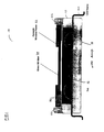
- Figure 1 shows a cross sectional block diagram of a windowed QFP package 10 that is mass reflowable.
- a non-ceramic mold package 12 makes up the package body.
- the non-ceramic mold package is made with a low-moisture plastic, such as a low-moisture mold compound of ortho-cresol-novolac developed by Kyocera Corporation.
- depressions 22 indicate where ejector pins were used to remove the mold package after being formed.
- Appendix 1 includes an example of the material characteristics of a low-moisture mold compound of Kyocera Corporation.
- Die attach 14 is used to hold the die 16 in place.
- the die attach 14 is a low rigidity epoxy such as a silver-filled epoxy manufactured by Ablestik Electronic Materials and Adhesives, based in Collinso Dominguez, California.
- Wire bonds 18 attach the die 16 to a lead frame 20.
- the die attach 14 is selected to withstand the elevated temperatures of the mass reflow process. Delamination of the die 16 from the die attach 14 or mold package 12 may be a problem during mass reflow. Applicants have determined that a two step cure process for the die attach, as will be discussed with respect to Figure 3, solves this problem.
- a lid 30 seals the mold package.
- the lid 30 comprises a ceramic frame 32 made of alumina.
- the ceramic frame 32 holds a transparent window.
- the ceramic frame 32 includes a recessed ledge within which a glass window 34 resides.
- the mold package 12 and the ceramic frame 32 are sealed using a bis-phenol A type epoxy.
- the epoxy seal may also be used to seal the ceramic frame 32 to the glass window 34.
- Appendix 2 summarizes the characteristics of a bis-phenol A-type sealant that is suitable for use with the present invention.
- the modified windowed package is particularly suited for, but not limited to, Complementary Metal Oxide Semiconductor (CMOS) image sensors because their die size can exceed 6 by 6 mm (240 by 240 mils).
- CMOS Complementary Metal Oxide Semiconductor
- An embodiment of the package suitable for an image sensor includes a window having a slightly larger area than that of the light-sensitive portion of the die.
- the window is approximately 1.2 times the area of the light-sensitive portion of the die.
- the window size varies depending on its distance away from the die.
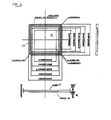
- Figures 2 and 3 shows schematic diagrams of one embodiment of the lid and mold package.
- Figure 2 shows a schematic of one embodiment of the package lid 30, including the ceramic frame 32 and glass window 34.
- the first dimension is in mils
- the dimension in parentheses is in millimeters.
- a glass window 34 is seated into a recessed ledge 40 in the ceramic frame 32.
- Figure 3 shows a schematic of one embodiment of the entire IC package 50 in accordance with present invention.
- the first dimension indicated for an element is in inches
- the second dimension (in parentheses) is in millimeters.
- lead frame quad flat pack -QFP
- other types of lead frames may be employed.
- other packages may be used, including leadless packages such as micro ball grid array (micro BGA), leadless chip carrier (LCC), dual inline package (DIP), and so forth.
- micro BGA micro ball grid array
- LCC leadless chip carrier
- DIP dual inline package
- Figure 4 shows the process steps taken in one embodiment of a method for attaching a die into a windowed non-ceramic package.
- die attach is dispensed on the mold package.
- the die attach is comprised of a low rigidity epoxy such as a silver-filled epoxy, as previously stated.
- the process continues at block 204, at which the die is scrubbed, or moved back and forth while pressure is applied to firmly attach the die to the die attach. Good adhesion of the die to a smooth surface of the mold package is achieved without plating the backside of the die with gold.
- the die attach is cured at block 206. It is important to eliminate voids in the die attach, which may cause delamination problems. It has been found that a two stage cure process works better than a one stage cure process for eliminating voids in the die attach. In one embodiment, the die attach is baked at approximately 100 degrees C for approximately one hour, then the die attach is baked at approximately 150 degrees C for approximately another hour.
- wire bonds are attached between the die and the lead frame of the mold package.
- the lid is attached to the mold package.
- the lid comprises the glass window 34 attached to the ceramic frame 32 with a bis-phenol A type epoxy.
- the epoxy is cured by baking. In one embodiment, the curing is performed by raising the temperature to approximately 150 degrees C for approximately 70 minutes.
- the lid is attached to the mold package using the same epoxy that was used to attach the glass window 34 to the ceramic frame 32, and the epoxy is cured by also raising the temperature to approximately 150 degrees C for approximately 70 minutes.
- the above steps are performed using laminar flow hoods in a clean room that meets level class sub 100, in which there is less than 100 particles of contamination of one micron or less per cubit meter. This helps to prevent particle contamination of the die during assembly.
- the window has a scratch-dig specification of 20 microns.
- the scratch-dig specification denotes the largest allowable defect in the glass. A larger defect may interfere with the imaging performance of the image sensor.
- the sealed package is baked at 125 degrees C for 48 hours, then it is vacuum sealed in a moisture barrier bag for storage or shipment. This allows the sealed package to meet the Institute for Interconnecting and Packaging Electronic Circuits (IPC) level 4 surface mount requirements. (The IPC is a trade association representing over 2300 companies in the electronic interconnection industry worldwide.)
- IPC Institute for Interconnecting and Packaging Electronic Circuits
- a mass reflow process As shown at block 214.
- mass reflow process There are various types of mass reflow processes.
- an ER/convection mass reflow process is employed that conforms to the following:
- the windowed non-ceramic package is able to withstand the above mass reflow process without the lid separating from the mold package or die detaching from the mold package.
- a pigmented color filter array (CFA) material is deposited on top of each photo-detector. Typically, one of the colors red, green or blue is deposited in a mosaic pattern. Pigments are chosen as the colorants over molecular dyes because of their superior light, heat, and chemical stability. Table 1 shows an example of the composition of the pigments used by Applicants. Applicant has found the CFA material to be extremely stable over various temperatures. This CFA material has previously been used in liquid crystal display (LCD) technology but has not been used as a color filter in image capture.
- LCD liquid crystal display
- Figure 5 shows one embodiment of the color filter process.
- the flowchart starts at block 300, and continues with block 310, at which the pigmented CFA material is deposited via a spin coat process.
- the spin coating is applied at 4000 RPM for approximately 30 seconds.
- the CFA is put through a soft bake phase in which the part is baked for about one minute at approximately 90 degrees C.
- the CFA is exposed.
- a mercury lamp of 500 W (I-line) is used.
- a post exposure bake of about three minutes at approximately 180 degrees C is performed at block 316.
- the CFA is developed. In one embodiment, the developing is performed at about 27 degrees C for approximately one minute to achieve a critical dimension of 20%.
- the part is then rinsed at block 320, then cured at block 322. Curing is performed for approximately 3 minutes at approximately 180 degrees C.
- a solvent of approximately 76wt% of propylene glycol monomethyl ether acetate (PGMEA) and approximately 5wt% of cyclohexanone is used to disperse the CFA material in the spin coating step (block 310), and a developer of between approximately. 13wt% and. 14wt% tetramethyl ammonium hydroxide is used in the developer step (block 318).
- PGMEA propylene glycol monomethyl ether acetate
- cyclohexanone cyclohexanone
- the flowchart steps are repeated for each of the different pigmented CFA materials.
- the flowchart steps are performed to apply a red, green then blue pigmented CFA material.
- various orders of applying the different colors of CFA materials may be used. Additionally, other color pigments may be used.
- the CFA material is deemed stable after the mass reflow process, if its color characteristics remain within a range that allows the image sensor to provide an image output of acceptable quality to a human observer.
- the color characteristics of the image sensor may shift slightly during mass reflow, but the shift in image output is still less than human perception, or b) the color characteristics of the image sensor shift during mass reflow, but the shift in image output can be compensated to provide an image that is acceptable to a human observer.
- a pass/fail threshold is based on ⁇ EL a*b* .
- the CFA material can be considered to be substantially stable only if its color difference changes by less than a ⁇ EL a*b* . of 5 from being exposed to the mass reflow process.
- ⁇ EL a*b* can be implemented as the pass/fail threshold.
- the average color for each of the channels red, green, and blue is measured by the image sensor before and after the mass reflow process.
- the color difference ⁇ EL a*b* is determined, as is well-known. For example, color difference ⁇ EL a*b* is described in Color Science: Concepts and Methods, Quantitative Data and Formulae, 2 nd edition, Gunter Wyszecki, W.S. Stiles (John Wiley & Sons, 1982).
- the CFA material also may be used to provide a scratch protection layer as described in co-pending U.S. patent application Serial Number 08/986,501, entitled “Passivation Protection On Sensor Devices During Electronic Assembly,” assigned to the common corporate assignee.
- a red pigment layer and a green pigment layer of CFA material having a thickness of approximately 600 microns is applied to the perimeter of a die to provide scratch protection of the underlying circuitry while handling the die.
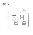
- Figure 6 shows an imaging system 400 comprising an image sensor attached to a circuit board via a mass reflow process.
- the image sensor 410 is employed as part of a camera, silicon eye, or other image device.
- the image sensor is electrically coupled to an image processor 420 and a memory 430.
- the imaging system may also include interconnect circuitry 440 for communicating with other systems, such as a host computer system or other output device.
- the imaging system may also include a lens system (not shown) to focus the light on the image sensor, as is well-known in the art.
- the ability to attach the image sensor via the mass reflow process reduces costs and speeds up the manufacturing process. It also may provide a more reliable connection then manual soldering methods.
- Pigment-dispersed Photopolymers Composition of Pigment-dispersed Photopolymers Composition Monomer Binder Initiator Pigment (main) Red: Diantraquinones Green: Halo-Cu-phthalocyanines Blue: Cu-phthalocyanines Black: Carbon Pigment (color matching) Yellow A :Isoindolins Yellow B : Diazo compounds violet : Dioxazines Solvent Cellusolves
- MATERIAL CHARACTERISTICS (GENERAL PROPERTIES OF E01B) PROPERTY NOMINAL VALUE THERMAL CONDUCTIVITY [ROOM TEMP.] 0.8 w/m ⁇ k THERMAL EXPANSION ( ⁇ 1) 150 ⁇ 10-7/°C, 490x 10-7 /°C BENDING STRENGTH 0.14 GPa BENDING ELASTICITY 18 GPa GLASS TRANSITION TEMPERATURE (Tg) 163°C VOLUME RESISTIVITY [ROOM TEMP.] 2 ⁇ 10 15 ⁇ ⁇ cm DIELECTRIC CONSTANT [1MHz] [ROOM TEMP.] 3.8 ⁇ COUNT EMISSION (DPH) 0.06 COUNTS / cm2 Hr
Landscapes
- Solid State Image Pick-Up Elements (AREA)
- Electric Connection Of Electric Components To Printed Circuits (AREA)
- Transforming Light Signals Into Electric Signals (AREA)
- Structures Or Materials For Encapsulating Or Coating Semiconductor Devices Or Solid State Devices (AREA)
Applications Claiming Priority (3)
| Application Number | Priority Date | Filing Date | Title |
|---|---|---|---|
| US172734 | 1998-10-13 | ||
| US09/172,734 US6753922B1 (en) | 1998-10-13 | 1998-10-13 | Image sensor mounted by mass reflow |
| PCT/US1999/023771 WO2000022814A2 (en) | 1998-10-13 | 1999-10-11 | Image sensor mounted by mass reflow |
Publications (3)
| Publication Number | Publication Date |
|---|---|
| EP1121799A2 EP1121799A2 (en) | 2001-08-08 |
| EP1121799A4 EP1121799A4 (en) | 2004-08-04 |
| EP1121799B1 true EP1121799B1 (en) | 2006-08-30 |
Family
ID=22628985
Family Applications (1)
| Application Number | Title | Priority Date | Filing Date |
|---|---|---|---|
| EP99970538A Expired - Lifetime EP1121799B1 (en) | 1998-10-13 | 1999-10-11 | Image sensor mounted by mass reflow |
Country Status (9)
| Country | Link |
|---|---|
| US (5) | US6753922B1 (https=) |
| EP (1) | EP1121799B1 (https=) |
| JP (1) | JP5201770B2 (https=) |
| KR (1) | KR100527897B1 (https=) |
| AU (1) | AU1444900A (https=) |
| DE (1) | DE69933040T2 (https=) |
| MY (1) | MY118657A (https=) |
| TW (1) | TW454411B (https=) |
| WO (1) | WO2000022814A2 (https=) |
Families Citing this family (66)
| Publication number | Priority date | Publication date | Assignee | Title |
|---|---|---|---|---|
| US6795120B2 (en) | 1996-05-17 | 2004-09-21 | Sony Corporation | Solid-state imaging apparatus and camera using the same |
| JPH1123613A (ja) * | 1997-07-04 | 1999-01-29 | Tokai Rika Co Ltd | ダイアフラム式センサチップを利用したセンサ |
| US6753922B1 (en) * | 1998-10-13 | 2004-06-22 | Intel Corporation | Image sensor mounted by mass reflow |
| US6307258B1 (en) * | 1998-12-22 | 2001-10-23 | Silicon Bandwidth, Inc. | Open-cavity semiconductor die package |
| US6297540B1 (en) * | 1999-06-03 | 2001-10-02 | Intel Corporation | Microlens for surface mount products |
| GB2355112A (en) * | 1999-10-08 | 2001-04-11 | Nokia Mobile Phones Ltd | Controlling bondwire inductance by using chip as positional reference |
| JP2001119006A (ja) * | 1999-10-19 | 2001-04-27 | Sony Corp | 撮像デバイス及びその製造方法 |
| US6483101B1 (en) * | 1999-12-08 | 2002-11-19 | Amkor Technology, Inc. | Molded image sensor package having lens holder |
| US6483030B1 (en) * | 1999-12-08 | 2002-11-19 | Amkor Technology, Inc. | Snap lid image sensor package |
| US6515269B1 (en) * | 2000-01-25 | 2003-02-04 | Amkor Technology, Inc. | Integrally connected image sensor packages having a window support in contact with a window and the active area |
| US6512219B1 (en) * | 2000-01-25 | 2003-01-28 | Amkor Technology, Inc. | Fabrication method for integrally connected image sensor packages having a window support in contact with the window and active area |
| WO2001091193A2 (en) | 2000-05-23 | 2001-11-29 | Atmel Corporation | Integrated ic chip package for electronic image sensor die |
| US6503780B1 (en) | 2000-07-05 | 2003-01-07 | Amkor Technology, Inc. | Wafer scale image sensor package fabrication method |
| US7059040B1 (en) | 2001-01-16 | 2006-06-13 | Amkor Technology, Inc. | Optical module with lens integral holder fabrication method |
| KR100401020B1 (ko) * | 2001-03-09 | 2003-10-08 | 앰코 테크놀로지 코리아 주식회사 | 반도체칩의 스택킹 구조 및 이를 이용한 반도체패키지 |
| JP3773177B2 (ja) * | 2001-11-30 | 2006-05-10 | 松下電器産業株式会社 | 固体撮像装置およびその製造方法 |
| US6825540B2 (en) * | 2001-12-05 | 2004-11-30 | Matsushita Electric Industrial Co., Ltd. | Miniaturized, resin-sealed solid state imaging apparatus |
| JP2003244560A (ja) * | 2002-02-21 | 2003-08-29 | Seiko Precision Inc | 固体撮像装置 |
| US6967123B2 (en) * | 2002-04-11 | 2005-11-22 | Agilent Technologies, Inc. | Adhesive die attachment method for a semiconductor die and arrangement for carrying out the method |
| US6906403B2 (en) | 2002-06-04 | 2005-06-14 | Micron Technology, Inc. | Sealed electronic device packages with transparent coverings |
| US7163838B2 (en) * | 2002-07-22 | 2007-01-16 | Texas Instruments Incorporated | Method and apparatus for forming a DMD window frame with molded glass |
| US7146106B2 (en) * | 2002-08-23 | 2006-12-05 | Amkor Technology, Inc. | Optic semiconductor module and manufacturing method |
| US7105383B2 (en) * | 2002-08-29 | 2006-09-12 | Freescale Semiconductor, Inc. | Packaged semiconductor with coated leads and method therefore |
| ITMI20022467A1 (it) * | 2002-11-20 | 2004-05-21 | St Microelectronics Srl | Processo per realizzare un transistore di selezione di byte per |
| EP1466875A3 (en) * | 2003-04-09 | 2007-05-30 | Hoya Corporation | Glass for window of semiconductor package, glass window for semiconductor package, process for production of glass window, and semiconductor package |
| JP3729817B2 (ja) * | 2003-04-28 | 2005-12-21 | 松下電器産業株式会社 | 固体撮像装置の製造方法 |
| US6874227B2 (en) * | 2003-06-03 | 2005-04-05 | Kingpak Technology Inc. | Method for packaging an image sensor |
| US7180064B2 (en) * | 2003-07-24 | 2007-02-20 | Delphi Technologies, Inc. | Infrared sensor package |
| US6953891B2 (en) * | 2003-09-16 | 2005-10-11 | Micron Technology, Inc. | Moisture-resistant electronic device package and methods of assembly |
| KR100539082B1 (ko) * | 2003-10-01 | 2006-01-10 | 주식회사 네패스 | 반도체 촬상소자의 패키지 구조 및 그 제조방법 |
| US20060261458A1 (en) * | 2003-11-12 | 2006-11-23 | Amkor Technology, Inc. | Semiconductor package and manufacturing method thereof |
| US7690303B2 (en) | 2004-04-22 | 2010-04-06 | Reynolds Systems, Inc. | Plastic encapsulated energetic material initiation device |
| TWI333249B (en) * | 2004-08-24 | 2010-11-11 | Himax Tech Inc | Sensor package |
| JP2006093588A (ja) * | 2004-09-27 | 2006-04-06 | Nec Electronics Corp | 表面に突起部を有する半導体装置および半導体パッケージの識別方法。 |
| US7359579B1 (en) | 2004-10-08 | 2008-04-15 | Amkor Technology, Inc. | Image sensor package and its manufacturing method |
| US7364945B2 (en) | 2005-03-31 | 2008-04-29 | Stats Chippac Ltd. | Method of mounting an integrated circuit package in an encapsulant cavity |
| US20070210246A1 (en) * | 2005-04-14 | 2007-09-13 | Amkor Technology, Inc. | Stacked image sensor optical module and fabrication method |
| US7227236B1 (en) | 2005-04-26 | 2007-06-05 | Amkor Technology, Inc. | Image sensor package and its manufacturing method |
| US20070272827A1 (en) * | 2005-04-27 | 2007-11-29 | Amkor Technology, Inc. | Image sensor package having mount holder attached to image sensor die |
| US7354800B2 (en) * | 2005-04-29 | 2008-04-08 | Stats Chippac Ltd. | Method of fabricating a stacked integrated circuit package system |
| US7576401B1 (en) | 2005-07-07 | 2009-08-18 | Amkor Technology, Inc. | Direct glass attached on die optical module |
| US7671478B2 (en) * | 2005-09-02 | 2010-03-02 | Honeywell International Inc. | Low height vertical sensor packaging |
| US7456088B2 (en) | 2006-01-04 | 2008-11-25 | Stats Chippac Ltd. | Integrated circuit package system including stacked die |
| US7768125B2 (en) | 2006-01-04 | 2010-08-03 | Stats Chippac Ltd. | Multi-chip package system |
| US7723146B2 (en) * | 2006-01-04 | 2010-05-25 | Stats Chippac Ltd. | Integrated circuit package system with image sensor system |
| US7750482B2 (en) | 2006-02-09 | 2010-07-06 | Stats Chippac Ltd. | Integrated circuit package system including zero fillet resin |
| US8704349B2 (en) | 2006-02-14 | 2014-04-22 | Stats Chippac Ltd. | Integrated circuit package system with exposed interconnects |
| US20080237824A1 (en) * | 2006-02-17 | 2008-10-02 | Amkor Technology, Inc. | Stacked electronic component package having single-sided film spacer |
| US7675180B1 (en) | 2006-02-17 | 2010-03-09 | Amkor Technology, Inc. | Stacked electronic component package having film-on-wire spacer |
| US7633144B1 (en) | 2006-05-24 | 2009-12-15 | Amkor Technology, Inc. | Semiconductor package |
| JP5132957B2 (ja) * | 2007-03-14 | 2013-01-30 | パナソニック株式会社 | 半導体デバイス、その製造方法および光ピックアップモジュール |
| DE102007026634B4 (de) * | 2007-06-06 | 2009-04-16 | Atotech Deutschland Gmbh | Vertikalanlage zur galvanotechnischen Behandlung eines Werkstückes und Verfahren zum Befördern des Werkstückes |
| SG152086A1 (en) * | 2007-10-23 | 2009-05-29 | Micron Technology Inc | Packaged semiconductor assemblies and associated systems and methods |
| JP2009176894A (ja) * | 2008-01-23 | 2009-08-06 | Panasonic Corp | 光学半導体装置 |
| US8100043B1 (en) | 2008-03-28 | 2012-01-24 | Reynolds Systems, Inc. | Detonator cartridge and methods of use |
| US7915717B2 (en) * | 2008-08-18 | 2011-03-29 | Eastman Kodak Company | Plastic image sensor packaging for image sensors |
| US8276516B1 (en) | 2008-10-30 | 2012-10-02 | Reynolds Systems, Inc. | Apparatus for detonating a triaminotrinitrobenzene charge |
| US8125042B2 (en) * | 2008-11-13 | 2012-02-28 | Samsung Electronics Co., Ltd. | Semiconductor package and method of manufacturing the same |
| US8485097B1 (en) | 2010-06-11 | 2013-07-16 | Reynolds Systems, Inc. | Energetic material initiation device |
| CN102136523B (zh) * | 2010-12-22 | 2012-11-28 | 木林森股份有限公司 | 眼珠型红外接收器的封装方法、专用模具及制造的产品 |
| US8941223B2 (en) * | 2012-09-10 | 2015-01-27 | Invensense, Inc. | MEMS device package with conductive shell |
| US8872296B2 (en) * | 2012-11-01 | 2014-10-28 | Lite-On Technology Corporation | Chip module structure for particles protection |
| EP3207566B1 (en) | 2014-10-13 | 2026-03-04 | Bio-Rad Laboratories, Inc. | Image sensor assembly with heated image sensor window |
| US9892935B2 (en) | 2015-05-28 | 2018-02-13 | International Business Machines Corporation | Limiting electronic package warpage with semiconductor chip lid and lid-ring |
| US10025033B2 (en) | 2016-03-01 | 2018-07-17 | Advanced Semiconductor Engineering, Inc. | Optical fiber structure, optical communication apparatus and manufacturing process for manufacturing the same |
| US10241264B2 (en) | 2016-07-01 | 2019-03-26 | Advanced Semiconductor Engineering, Inc. | Semiconductor device packages |
Citations (1)
| Publication number | Priority date | Publication date | Assignee | Title |
|---|---|---|---|---|
| US5471310A (en) * | 1990-08-27 | 1995-11-28 | Sierra Research And Technology, Inc. | System for placement and mounting of fine pitch integrated circuit devices |
Family Cites Families (55)
| Publication number | Priority date | Publication date | Assignee | Title |
|---|---|---|---|---|
| US4285002A (en) * | 1978-01-19 | 1981-08-18 | International Computers Limited | Integrated circuit package |
| JPS60115247A (ja) * | 1983-11-28 | 1985-06-21 | Fujitsu Ltd | 半導体装置 |
| JPS60239043A (ja) | 1984-05-14 | 1985-11-27 | Oki Electric Ind Co Ltd | 半導体装置用パツケ−ジの製造方法 |
| JPS60257546A (ja) * | 1984-06-04 | 1985-12-19 | Mitsubishi Electric Corp | 半導体装置及びその製造方法 |
| JPS6220358A (ja) | 1985-07-18 | 1987-01-28 | Nec Corp | 半導体固体撮像装置 |
| JPS6226847A (ja) * | 1985-07-27 | 1987-02-04 | Daiichi Seiko Kk | 気密封止形半導体装置 |
| JPS62174956A (ja) | 1986-01-28 | 1987-07-31 | Fujitsu Ltd | プラスチツク・モ−ルド型半導体装置 |
| US4827118A (en) * | 1986-07-10 | 1989-05-02 | Minolta Camera Kabushiki Kaisha | Light-sensitive device having color filter and manufacturing method thereof |
| JPS6333622A (ja) * | 1986-07-28 | 1988-02-13 | Minolta Camera Co Ltd | 受光素子接続構造及びその製造方法 |
| JPS6342150A (ja) | 1986-08-08 | 1988-02-23 | Hitachi Ltd | 光消去型樹脂封止型半導体装置 |
| US4771929A (en) * | 1987-02-20 | 1988-09-20 | Hollis Automation, Inc. | Focused convection reflow soldering method and apparatus |
| USRE37690E1 (en) * | 1987-02-25 | 2002-05-07 | Hitachi, Ltd. | Lead frame and semiconductor device |
| US5068712A (en) * | 1988-09-20 | 1991-11-26 | Hitachi, Ltd. | Semiconductor device |
| US4893171A (en) * | 1988-03-30 | 1990-01-09 | Director General, Agenty Of Industrial Science And Technology | Semiconductor device with resin bonding to support structure |
| US5468681A (en) * | 1989-08-28 | 1995-11-21 | Lsi Logic Corporation | Process for interconnecting conductive substrates using an interposer having conductive plastic filled vias |
| CA2047486C (en) * | 1990-07-21 | 2002-03-05 | Shigeru Katayama | Semiconductor device and method for manufacturing the same |
| US5168345A (en) * | 1990-08-15 | 1992-12-01 | Lsi Logic Corporation | Semiconductor device having a universal die size inner lead layout |
| US5627913A (en) * | 1990-08-27 | 1997-05-06 | Sierra Research And Technology, Inc. | Placement system using a split imaging system coaxially coupled to a component pickup means |
| US5147821A (en) * | 1990-09-28 | 1992-09-15 | Motorola, Inc. | Method for making a thermally enhanced semiconductor device by holding a leadframe against a heatsink through vacuum suction in a molding operation |
| US5227604A (en) * | 1991-06-28 | 1993-07-13 | Digital Equipment Corporation | Atmospheric pressure gaseous-flux-assisted laser reflow soldering |
| US5175410A (en) * | 1991-06-28 | 1992-12-29 | Digital Equipment Corporation | IC package hold-down fixture |
| FR2684803A1 (fr) | 1991-12-04 | 1993-06-11 | Gemplus Card Int | Boitier a structure renforcee pour circuit integre, et carte comprenant un tel boitier. |
| JP3203736B2 (ja) * | 1992-02-13 | 2001-08-27 | 株式会社日立製作所 | 液晶ドライバ用テープキャリアパッケージ及び液晶表示装置 |
| EP0646845B1 (en) * | 1992-06-19 | 2001-03-14 | Nippon Steel Corporation | Color filter, material thereof and resin |
| US5233222A (en) * | 1992-07-27 | 1993-08-03 | Motorola, Inc. | Semiconductor device having window-frame flag with tapered edge in opening |
| US5362680A (en) * | 1992-08-18 | 1994-11-08 | Texas Instruments Incorporated | Technique for enhancing adhesion capability of heat spreaders in molded packages |
| US5324888A (en) * | 1992-10-13 | 1994-06-28 | Olin Corporation | Metal electronic package with reduced seal width |
| US5536908A (en) * | 1993-01-05 | 1996-07-16 | Schlumberger Technology Corporation | Lead-free printed circuit assembly |
| US6326678B1 (en) | 1993-09-03 | 2001-12-04 | Asat, Limited | Molded plastic package with heat sink and enhanced electrical performance |
| DE9314355U1 (de) | 1993-09-22 | 1994-01-20 | ODS R. Oldenbourg Datensysteme GmbH, 81669 München | Chipkarten-Modul und Chipkarte |
| JPH07106351A (ja) * | 1993-10-04 | 1995-04-21 | Fujitsu Ltd | 半導体装置の製造方法 |
| US5498900A (en) * | 1993-12-22 | 1996-03-12 | Honeywell Inc. | Semiconductor package with weldable ceramic lid |
| EP0682988B1 (en) * | 1994-05-18 | 2001-11-14 | Xerox Corporation | Acoustic deposition of material layers |
| US5458716A (en) * | 1994-05-25 | 1995-10-17 | Texas Instruments Incorporated | Methods for manufacturing a thermally enhanced molded cavity package having a parallel lid |
| US5471011A (en) * | 1994-05-26 | 1995-11-28 | Ak Technology, Inc. | Homogeneous thermoplastic semi-conductor chip carrier package |
| US5828406A (en) * | 1994-12-30 | 1998-10-27 | Eastman Kodak Company | Electronic camera having a processor for mapping image pixel signals into color display pixels |
| JP3471111B2 (ja) * | 1995-03-20 | 2003-11-25 | 三菱電機株式会社 | 半導体装置 |
| JP3054576B2 (ja) * | 1995-04-26 | 2000-06-19 | シャープ株式会社 | 半導体装置 |
| JPH0992748A (ja) | 1995-09-21 | 1997-04-04 | Mitsubishi Materials Corp | 半導体素子用パッケージ |
| JP3292798B2 (ja) * | 1995-10-04 | 2002-06-17 | 三菱電機株式会社 | 半導体装置 |
| DE19618101A1 (de) | 1996-05-06 | 1997-11-13 | Siemens Ag | Trägerelement mit wenigstens einem integrierten Schaltkreis sowie Verfahren zur Herstellung eines solchen Trägerelementes |
| US5821617A (en) | 1996-07-29 | 1998-10-13 | Microsemi Corporation | Surface mount package with low coefficient of thermal expansion |
| US6028351A (en) * | 1996-10-09 | 2000-02-22 | Texas Instruments Incorporated | Gasket sealed integrated circuit package |
| US5786635A (en) * | 1996-12-16 | 1998-07-28 | International Business Machines Corporation | Electronic package with compressible heatsink structure |
| US5907769A (en) * | 1996-12-30 | 1999-05-25 | Micron Technology, Inc. | Leads under chip in conventional IC package |
| TW330337B (en) * | 1997-05-23 | 1998-04-21 | Siliconware Precision Industries Co Ltd | Semiconductor package with detached die pad |
| US5917709A (en) * | 1997-06-16 | 1999-06-29 | Eastman Kodak Company | Multiple circuit board assembly having an interconnect mechanism that includes a flex connector |
| JPH1197656A (ja) * | 1997-09-22 | 1999-04-09 | Fuji Electric Co Ltd | 半導体光センサデバイス |
| JP3123482B2 (ja) * | 1997-10-08 | 2001-01-09 | 日本電気株式会社 | 低熱抵抗型半導体パッケージ、および低熱抵抗型半導体パッケージの製造方法 |
| US6046075A (en) * | 1997-12-23 | 2000-04-04 | Vlsi Technology, Inc. | Oxide wire bond insulation in semiconductor assemblies |
| US6207947B1 (en) * | 1998-03-18 | 2001-03-27 | Intel Corporation | Using DUV curing to form a protective coating for color filters |
| JP3173586B2 (ja) * | 1998-03-26 | 2001-06-04 | 日本電気株式会社 | 全モールド型固体撮像装置およびその製造方法 |
| US6034423A (en) * | 1998-04-02 | 2000-03-07 | National Semiconductor Corporation | Lead frame design for increased chip pinout |
| US6191359B1 (en) | 1998-10-13 | 2001-02-20 | Intel Corporation | Mass reflowable windowed package |
| US6753922B1 (en) | 1998-10-13 | 2004-06-22 | Intel Corporation | Image sensor mounted by mass reflow |
-
1998
- 1998-10-13 US US09/172,734 patent/US6753922B1/en not_active Expired - Fee Related
- 1998-12-21 US US09/219,186 patent/US6072232A/en not_active Expired - Lifetime
-
1999
- 1999-10-08 TW TW088117423A patent/TW454411B/zh not_active IP Right Cessation
- 1999-10-11 EP EP99970538A patent/EP1121799B1/en not_active Expired - Lifetime
- 1999-10-11 KR KR10-2001-7004632A patent/KR100527897B1/ko not_active Expired - Fee Related
- 1999-10-11 DE DE69933040T patent/DE69933040T2/de not_active Expired - Lifetime
- 1999-10-11 AU AU14449/00A patent/AU1444900A/en not_active Abandoned
- 1999-10-11 WO PCT/US1999/023771 patent/WO2000022814A2/en not_active Ceased
- 1999-10-11 JP JP2000576612A patent/JP5201770B2/ja not_active Expired - Fee Related
- 1999-12-06 MY MYPI99005288A patent/MY118657A/en unknown
-
2000
- 2000-04-10 US US09/546,225 patent/US6692993B2/en not_active Expired - Fee Related
-
2004
- 2004-02-11 US US10/777,373 patent/US7026707B2/en not_active Expired - Fee Related
-
2006
- 2006-02-22 US US11/360,147 patent/US7223631B2/en not_active Expired - Fee Related
Patent Citations (1)
| Publication number | Priority date | Publication date | Assignee | Title |
|---|---|---|---|---|
| US5471310A (en) * | 1990-08-27 | 1995-11-28 | Sierra Research And Technology, Inc. | System for placement and mounting of fine pitch integrated circuit devices |
Also Published As
| Publication number | Publication date |
|---|---|
| EP1121799A4 (en) | 2004-08-04 |
| US20020125552A1 (en) | 2002-09-12 |
| US7026707B2 (en) | 2006-04-11 |
| US20040159902A1 (en) | 2004-08-19 |
| KR100527897B1 (ko) | 2005-11-15 |
| DE69933040D1 (de) | 2006-10-12 |
| WO2000022814A3 (en) | 2000-08-03 |
| JP5201770B2 (ja) | 2013-06-05 |
| US6753922B1 (en) | 2004-06-22 |
| US20060141674A1 (en) | 2006-06-29 |
| DE69933040T2 (de) | 2007-03-01 |
| EP1121799A2 (en) | 2001-08-08 |
| US7223631B2 (en) | 2007-05-29 |
| KR20010080129A (ko) | 2001-08-22 |
| WO2000022814A9 (en) | 2000-09-21 |
| JP2002527912A (ja) | 2002-08-27 |
| WO2000022814A2 (en) | 2000-04-20 |
| US6692993B2 (en) | 2004-02-17 |
| US6072232A (en) | 2000-06-06 |
| TW454411B (en) | 2001-09-11 |
| MY118657A (en) | 2004-12-31 |
| AU1444900A (en) | 2000-05-01 |
Similar Documents
| Publication | Publication Date | Title |
|---|---|---|
| EP1121799B1 (en) | Image sensor mounted by mass reflow | |
| US6191359B1 (en) | Mass reflowable windowed package | |
| US7345349B2 (en) | Solid state imaging device and producing method thereof | |
| TWI278121B (en) | FBGA and COB package structure for image sensor | |
| TWI264118B (en) | Covers for microelectronic imagers and methods for wafer-level packaging of microelectronic imagers | |
| US20060192230A1 (en) | Image sensor packages and frame structure thereof | |
| JP3956199B2 (ja) | 固体撮像装置の製造方法およびその製造方法において使用するマスク | |
| CN110416163A (zh) | 摄像器件模块、摄像系统、摄像器件封装和制造方法 | |
| KR100730726B1 (ko) | 카메라 모듈 | |
| JP2007536728A (ja) | 基板の背面上にパターニングされた層を有する電子パッケージ及びその製造方法 | |
| US20250048762A1 (en) | Semiconductor device, electronic apparatus, and manufacturing method of semiconductor device | |
| US20090179290A1 (en) | Encapsulated imager packaging | |
| KR100490692B1 (ko) | 내장 프레임을 가진 윈도우형 넌-세라믹 패키지 | |
| KR100840153B1 (ko) | 카메라 모듈 | |
| TWI842499B (zh) | 影像感測器模組 | |
| Sengupta et al. | Packaging requirements and solutions for CMOS imaging sensors | |
| TW558840B (en) | Image sensor of tape carrier package and method for manufacturing the same | |
| TW202447945A (zh) | 影像感測器封裝件及其製造方法 |
Legal Events
| Date | Code | Title | Description |
|---|---|---|---|
| PUAI | Public reference made under article 153(3) epc to a published international application that has entered the european phase |
Free format text: ORIGINAL CODE: 0009012 |
|
| 17P | Request for examination filed |
Effective date: 20010329 |
|
| AK | Designated contracting states |
Kind code of ref document: A2 Designated state(s): AT BE CH CY DE DK ES FI FR GB GR IE IT LI LU MC NL PT SE |
|
| RBV | Designated contracting states (corrected) |
Designated state(s): DE FR GB IT NL |
|
| A4 | Supplementary search report drawn up and despatched |
Effective date: 20040618 |
|
| 17Q | First examination report despatched |
Effective date: 20050531 |
|
| GRAP | Despatch of communication of intention to grant a patent |
Free format text: ORIGINAL CODE: EPIDOSNIGR1 |
|
| RIC1 | Information provided on ipc code assigned before grant |
Ipc: H01L 27/146 20060101ALI20060301BHEP Ipc: H04N 3/00 20060101AFI20060301BHEP |
|
| GRAS | Grant fee paid |
Free format text: ORIGINAL CODE: EPIDOSNIGR3 |
|
| GRAA | (expected) grant |
Free format text: ORIGINAL CODE: 0009210 |
|
| AK | Designated contracting states |
Kind code of ref document: B1 Designated state(s): DE FR GB IT NL |
|
| PG25 | Lapsed in a contracting state [announced via postgrant information from national office to epo] |
Ref country code: IT Free format text: LAPSE BECAUSE OF FAILURE TO SUBMIT A TRANSLATION OF THE DESCRIPTION OR TO PAY THE FEE WITHIN THE PRESCRIBED TIME-LIMIT;WARNING: LAPSES OF ITALIAN PATENTS WITH EFFECTIVE DATE BEFORE 2007 MAY HAVE OCCURRED AT ANY TIME BEFORE 2007. THE CORRECT EFFECTIVE DATE MAY BE DIFFERENT FROM THE ONE RECORDED. Effective date: 20060830 |
|
| REG | Reference to a national code |
Ref country code: GB Ref legal event code: FG4D |
|
| REF | Corresponds to: |
Ref document number: 69933040 Country of ref document: DE Date of ref document: 20061012 Kind code of ref document: P |
|
| EN | Fr: translation not filed | ||
| PLBE | No opposition filed within time limit |
Free format text: ORIGINAL CODE: 0009261 |
|
| STAA | Information on the status of an ep patent application or granted ep patent |
Free format text: STATUS: NO OPPOSITION FILED WITHIN TIME LIMIT |
|
| 26N | No opposition filed |
Effective date: 20070531 |
|
| PG25 | Lapsed in a contracting state [announced via postgrant information from national office to epo] |
Ref country code: FR Free format text: LAPSE BECAUSE OF FAILURE TO SUBMIT A TRANSLATION OF THE DESCRIPTION OR TO PAY THE FEE WITHIN THE PRESCRIBED TIME-LIMIT Effective date: 20070511 |
|
| PGFP | Annual fee paid to national office [announced via postgrant information from national office to epo] |
Ref country code: FR Payment date: 20061017 Year of fee payment: 8 |
|
| PG25 | Lapsed in a contracting state [announced via postgrant information from national office to epo] |
Ref country code: FR Free format text: LAPSE BECAUSE OF FAILURE TO SUBMIT A TRANSLATION OF THE DESCRIPTION OR TO PAY THE FEE WITHIN THE PRESCRIBED TIME-LIMIT Effective date: 20060830 |
|
| PGFP | Annual fee paid to national office [announced via postgrant information from national office to epo] |
Ref country code: DE Payment date: 20091028 Year of fee payment: 11 |
|
| PGFP | Annual fee paid to national office [announced via postgrant information from national office to epo] |
Ref country code: NL Payment date: 20091024 Year of fee payment: 11 |
|
| PGFP | Annual fee paid to national office [announced via postgrant information from national office to epo] |
Ref country code: GB Payment date: 20091026 Year of fee payment: 11 |
|
| REG | Reference to a national code |
Ref country code: NL Ref legal event code: V1 Effective date: 20110501 |
|
| GBPC | Gb: european patent ceased through non-payment of renewal fee |
Effective date: 20101011 |
|
| PG25 | Lapsed in a contracting state [announced via postgrant information from national office to epo] |
Ref country code: GB Free format text: LAPSE BECAUSE OF NON-PAYMENT OF DUE FEES Effective date: 20101011 Ref country code: NL Free format text: LAPSE BECAUSE OF NON-PAYMENT OF DUE FEES Effective date: 20110501 |
|
| REG | Reference to a national code |
Ref country code: DE Ref legal event code: R119 Ref document number: 69933040 Country of ref document: DE Effective date: 20110502 |
|
| PG25 | Lapsed in a contracting state [announced via postgrant information from national office to epo] |
Ref country code: DE Free format text: LAPSE BECAUSE OF NON-PAYMENT OF DUE FEES Effective date: 20110502 |