EP0933782B1 - Magnetisches Dünnfilmelement, Speicherelement damit und Schreibe- und Leseverfahren mit einem solchen Speicherelement - Google Patents
Magnetisches Dünnfilmelement, Speicherelement damit und Schreibe- und Leseverfahren mit einem solchen Speicherelement Download PDFInfo
- Publication number
- EP0933782B1 EP0933782B1 EP99300618A EP99300618A EP0933782B1 EP 0933782 B1 EP0933782 B1 EP 0933782B1 EP 99300618 A EP99300618 A EP 99300618A EP 99300618 A EP99300618 A EP 99300618A EP 0933782 B1 EP0933782 B1 EP 0933782B1
- Authority
- EP
- European Patent Office
- Prior art keywords
- magnetic
- magnetic layer
- memory
- layer
- thin film
- Prior art date
- Legal status (The legal status is an assumption and is not a legal conclusion. Google has not performed a legal analysis and makes no representation as to the accuracy of the status listed.)
- Expired - Lifetime
Links
Images


Classifications
-
- B—PERFORMING OPERATIONS; TRANSPORTING
- B82—NANOTECHNOLOGY
- B82Y—SPECIFIC USES OR APPLICATIONS OF NANOSTRUCTURES; MEASUREMENT OR ANALYSIS OF NANOSTRUCTURES; MANUFACTURE OR TREATMENT OF NANOSTRUCTURES
- B82Y10/00—Nanotechnology for information processing, storage or transmission, e.g. quantum computing or single electron logic
-
- G—PHYSICS
- G11—INFORMATION STORAGE
- G11C—STATIC STORES
- G11C11/00—Digital stores characterised by the use of particular electric or magnetic storage elements; Storage elements therefor
- G11C11/02—Digital stores characterised by the use of particular electric or magnetic storage elements; Storage elements therefor using magnetic elements
- G11C11/16—Digital stores characterised by the use of particular electric or magnetic storage elements; Storage elements therefor using magnetic elements using elements in which the storage effect is based on magnetic spin effect
- G11C11/165—Auxiliary circuits
- G11C11/1659—Cell access
-
- G—PHYSICS
- G11—INFORMATION STORAGE
- G11C—STATIC STORES
- G11C11/00—Digital stores characterised by the use of particular electric or magnetic storage elements; Storage elements therefor
- G11C11/02—Digital stores characterised by the use of particular electric or magnetic storage elements; Storage elements therefor using magnetic elements
- G11C11/16—Digital stores characterised by the use of particular electric or magnetic storage elements; Storage elements therefor using magnetic elements using elements in which the storage effect is based on magnetic spin effect
- G11C11/165—Auxiliary circuits
- G11C11/1673—Reading or sensing circuits or methods
-
- G—PHYSICS
- G11—INFORMATION STORAGE
- G11C—STATIC STORES
- G11C11/00—Digital stores characterised by the use of particular electric or magnetic storage elements; Storage elements therefor
- G11C11/02—Digital stores characterised by the use of particular electric or magnetic storage elements; Storage elements therefor using magnetic elements
- G11C11/16—Digital stores characterised by the use of particular electric or magnetic storage elements; Storage elements therefor using magnetic elements using elements in which the storage effect is based on magnetic spin effect
- G11C11/165—Auxiliary circuits
- G11C11/1675—Writing or programming circuits or methods
-
- H—ELECTRICITY
- H10—SEMICONDUCTOR DEVICES; ELECTRIC SOLID-STATE DEVICES NOT OTHERWISE PROVIDED FOR
- H10B—ELECTRONIC MEMORY DEVICES
- H10B61/00—Magnetic memory devices, e.g. magnetoresistive RAM [MRAM] devices
- H10B61/20—Magnetic memory devices, e.g. magnetoresistive RAM [MRAM] devices comprising components having three or more electrodes, e.g. transistors
- H10B61/22—Magnetic memory devices, e.g. magnetoresistive RAM [MRAM] devices comprising components having three or more electrodes, e.g. transistors of the field-effect transistor [FET] type
-
- H—ELECTRICITY
- H10—SEMICONDUCTOR DEVICES; ELECTRIC SOLID-STATE DEVICES NOT OTHERWISE PROVIDED FOR
- H10N—ELECTRIC SOLID-STATE DEVICES NOT OTHERWISE PROVIDED FOR
- H10N50/00—Galvanomagnetic devices
- H10N50/10—Magnetoresistive devices
Definitions
- the present invention relates to a magnetic thin film element making use of a giant magnetoresistive (GMR) effect, a memory element using the magnetic thin film element, and a method for recording and reproducing using the memory element.
- GMR giant magnetoresistive
- a magnetic thin film memory is a solid-state memory with no active part as is the case of a semiconductor memory
- information is not lost even if a power supply is cut off, writing is enabled repeatedly up to an unlimited number of times, and there is no danger that the memory content may vanish by the radiation, which are advantageous in comparison with the semiconductor memory.
- a thin film magnetic memory using the giant magnetoresistive (GMR) effect is receiving attention because of a larger output in comparison with a conventional thin film magnetic memory using an anisotropic magnetoresistive effect.
- a solid-state memory in which a memory element is fabricated by depositing for a plurality of times a structure including a hard magnetic layer (HM), a nonmagnetic layer (NM), a soft magnetic layer (SM), and a nonmagnetic layer (NM).
- HM hard magnetic layer
- NM nonmagnetic layer
- SM soft magnetic layer
- NM nonmagnetic layer
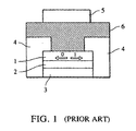
- FIG. 1 is a schematic sectional view showing a structure of such a solid-state memory.
- numeral 1 represents a hard magnetic layer
- numeral 2 represents a nonmagnetic layer
- numeral 3 represents a soft magnetic layer.
- a sense line 4 is provided on both sides of the magnetic film
- a word line 5 is provided being isolated from the sense line 4 by an insulating layer 6.
- An electric current is applied to the word line 5 and the sense line 4, and information is written by a magnetic field generated.
- FIGs. 2A through 2D by applying an electric current to the word line 5, a magnetic field is generated in a different direction in response to the direction of electric current represented by numeral 7.
- the magnetization of the hard magnetic layer 1 is reversed by the magnetic field to record a memory in a state of "0" or "1".
- the horizontal axis represents time T and the vertical axis represents electric current I.
- the same members as those in FIG. 1 are represented by the same numeral as in FIG. 1, and detailed descriptions will be omitted.
- a memory in a state of "1" is recorded as shown in FIB. 2B.
- a negative current as shown in FIG. 2C, to produce a leftward magnetic field, a memory in a state of "0" is recorded as shown in FIG. 2D.
- an electric current 7 that is smaller than the recording current is applied to the word line 5 to reverse the magnetization of the soft magnetic layer 3 only, and a change in resistance is detected.
- FIG. 3A the horizontal axis represents time T and the vertical axis represents electric current I. Also, in FIGs. 3B through 3E, the same members as those in FIG. 1 are represented by the same numeral as in FIG. 1, and detailed descriptions will be omitted.
- a memory in a state of "1" can be discriminated from a memory in a state of "0" in response to the change in resistance.
- a current is applied as a positive pulse and then as a negative pulse
- the magnetization of the soft magnetic layer 3 changes from rightward to leftward, and with respect to the memory in a state of "1”
- a small resistance as shown in FIG. 3B changes to a large resistance as shown in FIG. 3C.
- Patent Abstracts of Japan, vol. 1998, no. 10, 31 August 1998 and JP 10134560 discloses a magnetoresistive element in which CoCr 2 O is used for the first and second magnetic layers.
- US 5173873 discloses a magnetic memory element comprising, for example, bismuth, indium antimonide, nickel iron cobalt and permalloy or nickel iron.
- Patent Abstracts of Japan, vol. 1997, no. 4 and JP 08321016 discloses a magnetoresistive element comprising a lower magnetic layer , a non-magnetic intermediate layer and an upper magnetic layer, wherein the upper send lower magnetic layers show perpendicular magnetisations.
- EP-A- 0 507 451 describes (fig.50) a magnetic thin film element as indicated in the preamble of claim 1.
- a magnetic thin film elements comprising a magnetoresistive element comprising: a first magnetic layer ; a second magnetic layer having a higher coercive force than that of said first magnetic layer; and a non-magnetic layer interposed between said first magnetic layer and said second magnetic layer, said first magnetic layer and second magnetic layer each comprising a rare earth element and a transition element of the iron group, the magnetic thin film element being characterised in that said first and second magnetic layers (11,12) are in perpendicular magnetization states, and, in the perpendicular magnetization state, the resistance of said magnetoresistive element varies dependant on the magnetic moment of the transition element of the iron group of said first magnetic layer and the magnetic moment of the transition element of the iron group of said second magnetic layer.
- the nonmagnetic layer may be composed of a good conductor or an insulator.
- a memory element in another aspect, includes the magnetic thin film element described above and at least one write line composed of a good conductor provided in the vicinity of the magnetoresistive film of the magnetic thin film element with an insulator therebetween.
- a plurality of write lines may be provided on the sides of the magnetoresistive film.
- information may be retained in response to the direction of the magnetic spin of the first magnetic layer, and the direction of the magnetic spin of the second magnetic layer may always be maintained in the same direction. Alternatively, information may be retained in response to the direction of the magnetic spin of the second magnetic layer.
- a magnetic thin film memory in accordance with the present invention, includes a plurality of memory elements described above arrayed in a matrix on a substrate, and a magnetoresistive film of each memory element is electrically connected to a semiconductor device composed of a field effect transistor or a diode.
- a method for recording using the memory element includes applying an electric current to the write line, fixing a direction of the magnetic spin of the first magnetic layer by a magnetic field generated by the electric current, and changing the direction of an electric current to be applied to the write line to record a memory in a state of "0" or "1".
- a method for reproducing using the memory element includes detecting resistance of the magnetoresistive film to reproduce information recorded as the direction of the magnetic spin in the first magnetic layer.
- a method for recording using the memory element includes applying an electric current to the write line, fixing a direction of the magnetic spin of the second magnetic layer by a magnetic field generated by the electric current, and changing the direction of an electric current to be applied to the write line to record a memory in a state of "0" or "1".
- a method for reproducing using the memory element includes applying an electric current to the write line, and using a change in resistance resulting from the reversal of the magnetic spin of the first magnetic layer caused by a magnetic field generated by the electric current to reproduce information recorded in the second magnetic layer.
- FIGs. 4A and 4B are schematic sectional views showing a structure of a magnetic thin film element in accordance with a first embodiment of the present invention.
- Numeral 11 represents a first magnetic layer composed of a perpendicular magnetization film
- numeral 12 represents a second magnetic layer composed of a perpendicular magnetization film having a higher coercive force at room temperature in comparison with the first magnetic layer 11
- numeral 13 represents a nonmagnetic layer.
- the first magnetic layer 11 is deposited on the second magnetic layer 12 with the nonmagnetic layer 13 therebetween.
- the arrows represent magnetization direction, in particular, a direction of the spin constituting the magnetization.
- the magnetic spin directions of the first magnetic layer 11 and the second magnetic layer 12 are parallel, and in FIG. 4B, they are antiparallel.
- Materials for the first magnetic layer 11 and the second magnetic layer 12 include magnetic materials exhibiting perpendicular magnetization such as a ferrimagnetic film that is an alloy of a rare earth element and a transition element of the iron group (RE-TM), a garnet film that is an oxide magnetic film, an artificial lattice film of a rare earth element and a transition metal of the iron group (RE/TM), PtCo, and PdCo.
- a ferrimagnetic film that is an alloy of a rare earth element and a transition element of the iron group (RE-TM)
- a garnet film that is an oxide magnetic film an artificial lattice film of a rare earth element and a transition metal of the iron group (RE/TM)
- PtCo and PdCo.
- GdFe, GdFeCo, TbFe, TbFeCo, DyFe, DyFeCo, or the like is preferably used because of an easy exhibition of perpendicular magnetization.
- GdFe or GdFeCo is more preferable as a material for the first magnetic layer 11 because a coercive force can be decreased.
- TbFe, TbFeCo, DyFe, DyFeCo, or the like is preferably used because a coercive force can be increased, when the reversal of magnetization is caused by a magnetic field generated by an electric current, the required electric current value may be excessively large because of the excessively high coercive force in those materials, and thus, by using GdFe, GdFeCo, or the like, the composition is adjusted so that the second magnetic layer 12 has a larger coercive force than that of the first magnetic layer 11.
- resistance varies depending on whether the spin directions of the first magnetic layer 11 and the second magnetic layer 12 are parallel or antiparallel. For example, as shown in FIG. 4A, when the directions of the spins of the first magnetic layer 11 and the second magnetic layer 12 are parallel, resistance is low, and as shown in FIG. 4B, when the spin directions of the first magnetic layer 11 and the second magnetic layer 12 are antiparallel, resistance is high.
- FIGs. 5A and 5B using a RE-TM material.
- the same members as those in FIGs. 4A and 4B are represented by the same numeral as in FIGs. 4A and 4B, and detailed descriptions will be omitted.
- outlined arrows represent a net magnetization direction RM, which corresponds to a difference in magnetization between a rare earth element and an element of the iron group
- black arrows represent a magnetization direction IM of a transition element of the iron group.
- part of 3d electrons which contribute to the magnetization of the transition element of the iron group are conduction electrons because they are near an outer shell. Therefore, magneto-resistance depending on a difference in spin direction is more easily influenced by the spin of the transition element of the iron group. Accordingly, the spin direction caused by magneto-resistance depends on the spin direction of the element of the iron group. For example, as shown in FIG. 5A, when the magnetic moment of the element of the iron group of the first magnetic layer 11 is parallel to that of the second magnetic layer 12, resistance is small, and as shown in FIG. 5B, when antiparallel, resistance is large.
- transition element of the iron group-rich (TM-rich) structure is shown, in which the net magnetizations of the individual magnetic layers and the magnetization of the element of the iron group are in the same direction
- other structures may be used, for example, a structure in which the first magnetic layer 11 is rare earth element-rich (RE-rich) and the second magnetic layer 12 is TM rich, or vice versa.
- RE-rich rare earth element-rich
- the magnetic thin film element in the present invention is composed of a perpendicular magnetization film, in comparison with an element composed of an in-plane magnetization film, there is a large difference in stability of the magnetization when the element is finely structured.
- an element is composed of a known magnetoresistive film such as NiFe/Cu/Co
- an amount of saturation magnetization is approximately 800 emu/cc or more
- a demagnetizing field increases because magnetic poles on the ends of the film move closer to one another, and thus, the spins rotate at the film ends and are aligned parallel to the ends.
- an amount of demagnetizing energy is smaller than a perpendicular magnetic anisotropy constant, and therefore, an amount of saturation magnetization is suppressed at approximately 300 emu/cc or less at the maximum.
- the width of the element is decreased, magnetic poles on the ends of the film do not move closer to one another, and a demagnetizing field does not increase. Accordingly, even at a submicron width, magnetization can be maintained sufficiently stably. Therefore, when the element is used for a memory element, the integration can be significantly enhanced.
- a magnetic thin film element of this embodiment has the structure shown in FIGs. 4A and 4B, and a nonmagnetic layer 13 interposed between a first magnetic layer 11 and a second magnetic layer 12 is composed of a good conductor.
- This element is hereinafter referred to as a spin scattering element.
- a good conductor preferably has higher conductivity than that of the first magnetic layer 11 or the second magnetic layer 12, and, for example, Cu may be used.
- the nonmagnetic layer 13 has a thickness of 5 ⁇ to 60 ⁇ .
- the layer having Co as a major constituent preferably has a thickness of 5 ⁇ to 20 ⁇ .
- the thickness of the first magnetic layer 11 must be set so that a giant magnetoresistive effect is efficiently produced. Specifically, if the thickness of the first magnetic layer 11 largely exceeds a mean free path of electrons, the effect decreases because of phonon scattering, and thus the thickness is preferably at least 200 ⁇ or less, and more preferably 150 ⁇ or less. However, if the first magnetic layer 11 is excessively thin, resistance of the cell decreases, resulting in a decrease in output of playback signals as well as difficulty in retaining the magnetization. Therefore, the thickness of the first magnetic layer 11 is preferably 20 ⁇ or more, and more preferably 80 ⁇ or more.
- the thickness of the second magnetic layer 12 is set so that a giant magnetoresistive effect is efficiently produced, the same as the first magnetic layer 11, the thickness is preferably 200 ⁇ or less, and more preferably 150 ⁇ or less. However, if the thickness is excessively small, resistance of the cell decreases, resulting in a decrease in output of playback signals as well as difficulty in retaining the magnetization. Therefore, the thickness of the second magnetic layer 12 is preferably 20 ⁇ or more, and more preferably 80 ⁇ or more.
- a unit including a first magnetic layer, a nonmagnetic layer, a second magnetic layer and a nonmagnetic layer may be deposited a plurality of times.
- a magneto-resistance ratio increases, which is preferable.
- the number of units to be deposited is preferably 40 or less, and more preferably approximately 3 to 20.
- a magnetic thin film element of this embodiment has the structure shown in FIGs. 4A and 4B, and a nonmagnetic layer 13 interposed between a first magnetic layer 11 and a second magnetic layer 12 is composed of an insulator, and thus a spin-tunnel film is formed.
- a spin-tunnel film is formed.
- a ferromagnetic tunnel junction which includes a ferromagnetic material, an insulator, and a ferromagnetic material, is formed. Since conduction electrons of the ferromagnetic materials tunnel while maintaining the spins, tunnel probability varies depending on the magnetization condition of both magnetic layers, resulting in a change in tunnel resistance. Accordingly, when the magnetizations of the first magnetic layer 11 and the second magnetic layer 12 are parallel, resistance is small, and when the magnetizations of the first magnetic layer 11 and the second magnetic layer 12 is antiparallel, resistance is large. As a difference in density of states between upward spins and downward spins increases, the resistance increases, resulting in larger output signals.
- a magnetic material having high spin polarizability is preferably used for the first magnetic layer 11 and the second magnetic layer 12.
- Fe which has high polarizability of upward and downward spins at the Fermi surface, is selected as a major constituent, and Co is selected as a second constituent.
- the thickness of the magnetic thin film element of this embodiment is preferably from 100 ⁇ to 5,000 ⁇ .
- the reason for this is that, firstly, when an oxide is used as the insulator, since magnetism at the interface between the magnetic layer and the oxide is weakened under the influence of the oxide, the portion with weakened magnetism dominates in the entire film if the thickness is small, resulting in an adverse effect to the magnetism of the film.
- a memory element is refined to the submicron range, since volumes of the first magnetic layer 11 and the second magnetic layer 12 decrease, perpendicular magnetic anisotropic energy decreases, resulting in a decrease in the magnetization retention function of the individual layers. Also, if the thickness is excessively large, resistance of the cell increases excessively.
- the thickness is preferably 5,000 ⁇ or less, and more preferably, 1,000 ⁇ or less.
- the nonmagnetic layer 13 since the magnetic thin film element of this embodiment uses the magnetoresistive effect by spin-tunneling, the nonmagnetic layer 13 must be an insulating layer so that electrons tunnel while retaining spins.
- the nonmagnetic layer 13 may be entirely insulating, or may be partially insulating.
- An example in which an oxide layer composed of an oxidized nonmagnetic metal film is used as the nonmagnetic layer 13 includes an Al 2 O 3 layer formed by oxidizing a portion of an Al film in air or in a vacuum by plasma oxidation.
- AlNx aluminum nitride
- SiOx silicon oxide
- SiNx silicon nitride
- NiOx nickel oxide
- AlOx aluminum oxide
- an appropriate potential barrier is required to the energy of conduction electrons of the first and the second magnetic layers.
- the materials mentioned above relatively easily produce the barrier, which is advantageous in production.
- the nonmagnetic layer 13 is a uniform layer having a thickness of approximately several tens of ⁇ , and the thickness of its insulating portion has a thickness from 5 ⁇ to 30 ⁇ . If the thickness is less than 5 ⁇ , there is a possibility of an electrical short circuit between the first magnetic layer 11 and the second magnetic layer 12. If the thickness is more than 30 ⁇ , tunneling of electrons do not easily occur. More preferably, the thickness is 4 ⁇ to 25 ⁇ , and still more preferably, the thickness is 6 ⁇ to 18 ⁇ .
- One of the applications of a magnetic thin film element in accordance with the present invention is an application to a memory element, which records information of "0" or "1" in response to the magnetization direction, and reads information using a difference in resistance.
- FIG. 6 is a schematic sectional view showing a memory element which uses the magnetic thin film element described above.
- the same members as those in FIGs. 4A and 4B are represented by the same numeral as in FIGs. 4A and 4B, and detailed descriptions will be omitted.
- Numeral 14 represents the magnetic thin film element shown in FIGs. 4A and 4B
- numeral 15 represents a write line composed of a good conductor
- numeral 16 represents a magnetic field generated by applying an electric current to the write line 15.
- magnetization information "0" or "1" is recorded in response to the spin direction, i.e., upward or downward, of either the first magnetic layer 11 or the second magnetic layer 12. Whether information is stored in the first magnetic layer 11 or in the second magnetic layer 12 depends on a structure of the element which will be described below.
- recording is performed by applying an electric current to the write line 15 placed in the vicinity of the first and second magnetic layers 11 and 12, and reversing the magnetization of the first magnetic layer 11 or the second magnetic layer 12 by the magnetic field 16 generated.
- an electric current is applied toward the drawing, if the electric current is applied in reverse, a reversed magnetic field is generated and the direction of the spin can be reversed.
- Whether information is recorded in the first magnetic layer 11 or in the second magnetic layer 12 depends on a medium type as described below.
- An insulating film (not shown in the drawing) is provided between the write line 15 and the magnetoresistive film 14. The insulating film is provided in order to prevent the write line 15 and the magnetoresistive film 14 from being electrically connected to each other. The deterioration of playback signals caused by the leakage of an electric current applied to the magnetic thin film element to the write line 15 can be prevented.
- the magnetoresistive film 14 exhibits low resistance when the spin of the first magnetic layer 11 and the spin of the second magnetic layer 12 are parallel, and exhibits high resistance when they are antiparallel. Therefore, digital information recorded can be detected by detecting the resistance of the magnetoresistive film or a change in the resistance, as described below.
- the write line 15 is set so that a magnetic field is generated perpendicular to the magnetoresistive film 14 by applying an electric current.
- the write line 15 is preferably placed so that an electric current is applied parallel to the film surface.
- the space is at least from 10 ⁇ to 1 ⁇ m, and preferably, from 50 ⁇ to 1,000 ⁇ .
- a magnetic thin film memory element of this embodiment has the structure shown in FIG. 6, and includes a memory layer (first magnetic layer 11), a nonmagnetic layer 13, and a pinned layer (second magnetic layer 12).
- the first magnetic layer 11 is a memory layer for storing magnetic information
- the second magnetic layer 12 is a pinned layer in which the magnetization is always aligned in a predetermined direction in any state of storing, recording, and reproducing.
- a method of recording will be described with reference to the FIGs. 4A and 4B.
- Data of "0" and "1" are set to correspond to the upward magnetization of the first magnetic layer 11 (FIG. 4A) and the downward magnetization (FIG. 4B), respectively.
- the magnetization of the first magnetic layer 11 is reversed by a magnetic field generated by an electric current to be applied to a write line 15.
- a magnetic field generated by an electric current to be applied to a write line 15.
- spin direction of the second magnetic layer 12 is upward in the above, it may be downward. Also, data of "0" and "1" may be set to correspond to the downward magnetization of the first magnetic layer 11 and the upward magnetization, respectively.
- the RE-TM materials described above may be used, with respect to the second magnetic layer 12 as the pinned layer, TbFe, TbFeCo, DyFe, DyFeCo, or the like having a high coercive force is preferably used. Additionally, by providing an antiferromagnetic material such as FeMn, IrMn, or NiO on the second magnetic layer 12 on the opposite side to the interface with the nonmagnetic layer in order to increase the coercive force of the second magnetic layer 12.
- an antiferromagnetic material such as FeMn, IrMn, or NiO
- the coercive force of the first magnetic layer 11 is preferably from 5 Oe to 50 Oe. If the coercive force of the second magnetic layer 12 is too low, there is a possibility of the reversal of the magnetization during recording and reproducing, and if it is too high, it is difficult to perform initialization in which the spin is aligned in one direction. Accordingly, the coercive force of the second magnetic layer 12 is preferably from 20 Oe to 20 kOe. Also, the coercive force of the first magnetic layer 11 is preferably set at approximately half of that of the second magnetic layer 12.
- a magnetic thin film memory element of this embodiment has the structure shown in FIG. 6, and includes a detection layer (first magnetic layer 11), a nonmagnetic layer 13, and a memory layer (second magnetic layer 12).
- the second magnetic layer 12 is a memory layer for storing magnetic information
- the first magnetic layer 11 having a small coercive force is provided for reading the magnetic information stored in the second magnetic layer 12 using a magnetoresistive effect.
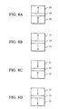
- FIGs. 8A through 8D illustrate the magnetization of such a magnetic thin film memory element during recording and reproducing.
- the same members as those in FIGs. 4A and 4B are represented by the same numeral as in FIGs. 4A and 4B, and detailed descriptions will be omitted.
- the arrows represent the direction of the magnetic spin of the individual magnetic layers.
- data of "0" and “1" are set to correspond to the upward magnetization of the second magnetic layer 12 (FIG. 8A) and the downward magnetization (FIG. 8B), respectively.
- the magnetization of the second magnetic layer 12 is reversed by a magnetic field generated by recording current.
- an electric current which is weaker than that during recording is applied to a write line, or, as described below, an electric current is applied to only one of two write lines provided, to generate a magnetic field which is smaller than that during recording, and the magnetization of the detection layer only is reversed without reversing the magnetization of the memory layer.
- the magnetization is changed from a state shown in FIG. 8A to a state shown in FIG. 8C, or in reverse.
- the magnetization is changed from a state shown in FIG. 8B to a state shown in FIG. 8D, or in reverse. Resistance changes from low to high in the case of "0", and changes from high to low in the case of "1".
- recorded information can be detected by a change in resistance.
- even a minute change in signals can be detected using a differential detection or the like, in comparison with the method of detecting the absolute value of resistance, and thus, reproducing can be performed with high detectivity.
- data of "0" and “1" may be set to correspond to the downward magnetization of the second magnetic layer 12 and the upward magnetization, respectively.
- the RE-TM materials described above may be used, since the magnetization of both layers is reversed during recording and reproducing, GdFe, GdFeCo, or the like having a lower coercive force is preferably used.
- the coercive force of the first magnetic layer 11 is preferably from 2 Oe to 20 Oe. If the coercive force of the second magnetic layer 12 is too low, memory characteristics deteriorate, and if it is too high, recording current increases. Accordingly, the coercive force of the second magnetic layer 12 is preferably from 5 Oe to 50 Oe. Also, the coercive force of the first magnetic layer 11 is preferably set at approximately half of that of the second magnetic layer 12.
- numeral 14 represents the magnetic thin film element shown in FIGs. 4A and 4B
- numerals 17 and 18 are write lines composed of a good conductor
- numerals 19 and 20 are magnetic fields generated by applying an electric current to the write lines 17 and 18, respectively.
- a weaker magnetic field is generated during reproducing in comparison with during recording. Therefore, by applying an electric current to one write line during reproducing and by applying an electric current to two write lines during recording, a current margin between reproducing and recording can be increased, resulting in the stable operation with no recording errors during reproducing.
- a plurality of one-bit memory cells including magnetic thin film elements in accordance with the present invention are arrayed in a matrix to constitute the entire memory.
- a write line and a selector transistor are provided on each cell, integration decreases.
- a common write line is preferably provided on a plurality of cells.
- an electric current when an electric current is applied to the write line, a magnetic field is applied to a plurality of memory cells at the same time. Therefore, it is required to make a structure in which the magnetization of one memory cell only can be reversed, for example, by applying an electric current to the memory cell to be recorded.
- an active element such as a field effect transistor may be used for applying an electric current independently to a memory cell during reproducing.
- an electric current can be applied selectively to one memory cell among many memory cells in the vicinity of the write line.
- the electric current path can be the same as that of reproducing and is perpendicular to an electric current applied to the write line, a magnetic field generated by the electric current is perpendicular to a magnetic field generated by the write line, and thus, the memory cell selected by the active element is applied a larger resultant magnetic field in comparison with other memory cells, resulting in reversal of magnetization.
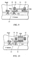
- FIGs. 9 and 10 illustrate such memory cells in which one end of a magnetic thin film element is connected to a transistor and the other end is connected to a source voltage VDD.
- numeral 21 represents a magnetic thin film element
- numerals 22 and 23 represent write lines
- numeral 24 represents a transistor
- numeral 25 represents a control gate.
- numeral 31 represents a magnetic thin film element
- numerals 32 and 33 represent write lines
- numeral 34 represents a transistor
- numeral 35 represents a control gate.
- a read line composed of a good conductor is connected to the end of the magnetoresistive film 21 or 31, and a sense circuit or the like is connected so that a change in resistance can be detected.
- Write lines 22, 23, 32, and 33 are provided in the vicinity of the magnetoresistive films 21 and 31 with an insulator composed of SiO 2 , SiNx or the like therebetween.
- the write lines are placed perpendicular to the drawing and used for writing other memory cells (not shown in the drawing).
- the reproducing electric current path is horizontal in FIG. 9, and perpendicular in FIG 10.
- the structure as shown in FIG 10 is adopted.
- the spin scattering element either structure may be adopted, preferably the structure as shown in FIG. 9, in which the electric current is applied horizontally, is used since the absolute value of resistance decreases in the structure as shown in FIG. 10 in which the electric current is applied perpendicular to the film surface.
- the magnetization of the detection layer can be reversed by applying a magnetic field to the magnetic thin film element of a specific memory cell in the same manner as that during recording.
- a change in resistance occurs and the change is amplified by the sense circuit to be detected.
- information in a specific memory cell among many memory cells can be read.
- the resistance of the element selected by the active element is amplified by the sense circuit for detection.
- the magnetic thin film element and the magnetic thin film memory element described in the embodiments may be used for a magnetic sensor, or a magnetic head of a hard disk or the like.
Landscapes
- Engineering & Computer Science (AREA)
- Computer Hardware Design (AREA)
- Chemical & Material Sciences (AREA)
- Nanotechnology (AREA)
- Crystallography & Structural Chemistry (AREA)
- Theoretical Computer Science (AREA)
- Mathematical Physics (AREA)
- Physics & Mathematics (AREA)
- Mram Or Spin Memory Techniques (AREA)
- Hall/Mr Elements (AREA)
- Semiconductor Memories (AREA)
- Thin Magnetic Films (AREA)
- Measuring Magnetic Variables (AREA)
- Magnetic Heads (AREA)
Claims (14)
- Magnetisches Dünnfilmelement mit einem Magnetwiderstandselement, das Folgendes umfasst:eine erste Magnetschicht (11);eine zweite Magnetschicht (12), die eine höhere Koerzitivkraft als die erste Magnetschicht (11) hat; undeine nichtmagnetische Schicht (13), die zwischen der ersten Magnetschicht (11) und der zweiten Magnetschicht (12) angeordnet ist,wobei die erste Magnetschicht (11) und die zweite Magnetschicht (12) jeweils ein Seltenerdelement und ein Übergangselement der Eisengruppe umfassen und wobei das magnetische Dünnfilmelement dadurch gekennzeichnet ist, dass
sich die erste und zweite Magnetschicht (11, 12) in senkrechten Magnetisierungszuständen befinden und
sich der Widerstand des Magnetwiderstandselements im senkrechten Magnetisierungszustand abhängig vom magnetischen Moment des Übergangselements der Eisengruppe der ersten Magnetschicht (11) und des magnetischen Moments des Übergangselements der Eisengruppe der zweiten Magnetschicht (12) ändert. - Magnetisches Dünnfilmelement nach Anspruch 1, bei dem die nichtmagnetische Schicht (13) einen guten Leiter umfasst.
- Magnetisches Dünnfilmelement nach Anspruch 1, bei dem die nichtmagnetische Schicht (13) einen Isolator umfasst.
- Speicherelement mit:einem magnetischen Dünnfilmelement (14) gemäß Anspruch 1; undmindestens einer einen guten Leiter umfassenden Schreibleitung (15), die sich mit einem Isolator dazwischen in der Nähe eines Magnetwiderstandsfilms des magnetischen Dünnfilmelements (14) befindet.
- Speicherelement nach Anspruch 4, bei dem sich auf den Seiten des Magnetwiderstandsfilmelements (14) eine Vielzahl von Schreibleitungen (17, 18) befindet.
- Speicherelement nach Anspruch 4, bei dem im Ansprechen auf die Richtung des magnetischen Spins der ersten Magnetschicht (11) Informationen bewahrt werden und die Richtung des magnetischen Spins der zweiten Magnetschicht (12) stets in der gleichen Richtung gehalten wird.
- Speicherelement nach Anspruch 4, bei dem im Ansprechen auf die Richtung des magnetischen Spins der zweiten Magnetschicht (12) Informationen bewahrt werden.
- Magnetischer Dünnfilmspeicher mit:einer Vielzahl von Speicherelementen gemäß Anspruch 4, die auf einem Substrat (24; 34) in einer Matrix angeordnet sind,wobei ein Magnetwiderstandsfilm jedes dieser Speicherelemente elektrisch mit einem Halbleiterbauelement verbunden ist, das entweder einen Feldeffekttransistor oder eine Diode umfasst.
- Verfahren zum Aufzeichnen mittels eines Speicherelements gemäß Anspruch 6, mit den Schritten:Anlegen eines elektrischen Stroms an die Schreibleitung (15);Festlegen einer Richtung des magnetischen Spins der ersten Magnetschicht (11) durch ein von dem elektrischen Strom erzeugtes Magnetfeld; undVersetzen eines Speichers in einen Zustand von entweder "0" oder "1" durch Ändern der Richtung eines auf die Schreibleitung (15) aufzubringenden elektrischen Stroms.
- Verfahren zum Wiedergeben mittels eines Speicherelements gemäß Anspruch 6, mit den Schritten:Erfassen des Widerstands des Magnetwiderstandsfilmelements, um Informationen wiederzugeben, die in der ersten Magnetschicht (11) als Richtung des magnetischen Spins aufgezeichnet sind.
- Verfahren zum Aufzeichnen mittels eines Speicherelements gemäß Anspruch 7, mit den Schritten:Anlegen eines elektrischen Stroms an die Schreibleitung (15);Festlegen einer Richtung des magnetischen Spins der zweiten Magnetschicht (12) durch ein von dem elektrischen Strom erzeugtes Magnetfeld; undVersetzen eines Speichers in einen Zustand von entweder "0" oder "1" durch Ändern der Richtung eines auf die Schreibleitung (15) aufzubringenden elektrischen Stroms.
- Verfahren zum Wiedergeben mittels eines Speicherelements gemäß Anspruch 7, mit den Schritten:Anlegen eines elektrischen Stroms an die Schreibleitung (15);Nutzen einer Widerstandsänderung infolge der Umkehr des magnetischen Spins der ersten Magnetschicht (11), die durch ein von dem elektrischen Strom erzeugtes Magnetfeld verursacht wird, um in der zweiten Magnetschicht (12) aufgezeichnete Informationen wiederzugeben.
- Magnetisches Dünnfilmelement nach Anspruch 1, bei dem sich der Widerstand des Magnetwiderstandfilms abhängig davon ändert, ob die magnetischen Spins der ersten Magnetschicht und der zweiten Magnetschicht in derselben Richtung liegen oder nicht, und die nichtmagnetische Schicht einen Isolator umfasst, der eine Dicke von 0,5 nm bis 3 nm hat.
- Magnetisches Dünnfilmelement nach Anspruch 1, bei dem sich der Widerstand des Magnetwiderstandfilms abhängig davon ändert, ob die magnetischen Spins der ersten Magnetschicht (11) und der zweiten Magnetschicht (12) derselben Richtung liegen oder nicht, und die nichtmagnetische Schicht (13) einen guten Leiter umfasst und die erste Magnetschicht (11) und die zweite Magnetschicht (12) eine Dicke von 2 nm bis 20 nm haben.
Applications Claiming Priority (2)
| Application Number | Priority Date | Filing Date | Title |
|---|---|---|---|
| JP01563398A JP3679593B2 (ja) | 1998-01-28 | 1998-01-28 | 磁性薄膜素子および磁性薄膜メモリ素子およびその記録再生方法 |
| JP1563398 | 1998-01-28 |
Publications (3)
| Publication Number | Publication Date |
|---|---|
| EP0933782A2 EP0933782A2 (de) | 1999-08-04 |
| EP0933782A3 EP0933782A3 (de) | 2000-05-03 |
| EP0933782B1 true EP0933782B1 (de) | 2006-08-23 |
Family
ID=11894134
Family Applications (1)
| Application Number | Title | Priority Date | Filing Date |
|---|---|---|---|
| EP99300618A Expired - Lifetime EP0933782B1 (de) | 1998-01-28 | 1999-01-27 | Magnetisches Dünnfilmelement, Speicherelement damit und Schreibe- und Leseverfahren mit einem solchen Speicherelement |
Country Status (4)
| Country | Link |
|---|---|
| US (4) | US6219275B1 (de) |
| EP (1) | EP0933782B1 (de) |
| JP (1) | JP3679593B2 (de) |
| DE (1) | DE69932872T2 (de) |
Families Citing this family (73)
| Publication number | Priority date | Publication date | Assignee | Title |
|---|---|---|---|---|
| JP3679593B2 (ja) * | 1998-01-28 | 2005-08-03 | キヤノン株式会社 | 磁性薄膜素子および磁性薄膜メモリ素子およびその記録再生方法 |
| EP0959475A3 (de) * | 1998-05-18 | 2000-11-08 | Canon Kabushiki Kaisha | Magnetischer Dünnfilmspeicher sowie Schreibe- und Leseverfahren und Anordnung unter Verwendung solchen Speichers |
| JP3559722B2 (ja) | 1999-04-16 | 2004-09-02 | キヤノン株式会社 | 磁気抵抗素子、固体メモリ |
| US6611405B1 (en) | 1999-09-16 | 2003-08-26 | Kabushiki Kaisha Toshiba | Magnetoresistive element and magnetic memory device |
| JP2001084758A (ja) * | 1999-09-17 | 2001-03-30 | Fujitsu Ltd | 強磁性トンネル接合ランダムアクセスメモリ、スピンバルブランダムアクセスメモリ、単一強磁性膜ランダムアクセスメモリ、およびこれらをつかったメモリセルアレイ |
| US6778425B1 (en) * | 1999-09-27 | 2004-08-17 | Matsushita Electric Industrial Co., Ltd. | Magnetoresistance effect memory device and method for producing the same |
| EP1115164B1 (de) | 2000-01-07 | 2005-05-25 | Sharp Kabushiki Kaisha | Magnetoresistive Anordnung und diese verwendendes magnetisches Speicherelement |
| DE10040811A1 (de) * | 2000-08-21 | 2002-03-14 | Infineon Technologies Ag | Monolithisch integrierbare Induktivität |
| US7035138B2 (en) * | 2000-09-27 | 2006-04-25 | Canon Kabushiki Kaisha | Magnetic random access memory having perpendicular magnetic films switched by magnetic fields from a plurality of directions |
| JP3524486B2 (ja) | 2000-10-13 | 2004-05-10 | キヤノン株式会社 | 磁気抵抗素子及び該素子を用いたメモリ素子 |
| TW544677B (en) * | 2000-12-26 | 2003-08-01 | Matsushita Electric Ind Co Ltd | Magneto-resistance memory device |
| JP4666774B2 (ja) * | 2001-01-11 | 2011-04-06 | キヤノン株式会社 | 磁気薄膜メモリ素子、磁気薄膜メモリおよび情報記録再生方法 |
| JP4666775B2 (ja) * | 2001-01-11 | 2011-04-06 | キヤノン株式会社 | 磁気薄膜メモリ素子、磁気薄膜メモリおよび情報記録方法 |
| JP3667244B2 (ja) | 2001-03-19 | 2005-07-06 | キヤノン株式会社 | 磁気抵抗素子、それを用いたメモリ素子、磁気ランダムアクセスメモリ及び磁気ランダムアクセスメモリの記録再生方法 |
| US6713830B2 (en) * | 2001-03-19 | 2004-03-30 | Canon Kabushiki Kaisha | Magnetoresistive element, memory element using the magnetoresistive element, and recording/reproduction method for the memory element |
| JP4944315B2 (ja) * | 2001-08-13 | 2012-05-30 | キヤノン株式会社 | 磁気抵抗効果膜、それを備えたメモリ素子及びそれを用いたメモリ |
| TW560095B (en) | 2001-04-02 | 2003-11-01 | Canon Kk | Magnetoresistive element, memory element having the magnetoresistive element, and memory using the memory element |
| US6611455B2 (en) | 2001-04-20 | 2003-08-26 | Canon Kabushiki Kaisha | Magnetic memory |
| JP3482469B2 (ja) * | 2001-05-21 | 2003-12-22 | 北海道大学長 | 磁気記憶素子、磁気メモリ、磁気記録方法、磁気記憶素子の製造方法、及び磁気メモリの製造方法 |
| JP2002368306A (ja) | 2001-06-07 | 2002-12-20 | Canon Inc | 磁気抵抗効果膜およびそれを用いたメモリ |
| DE10128964B4 (de) * | 2001-06-15 | 2012-02-09 | Qimonda Ag | Digitale magnetische Speicherzelleneinrichtung |
| US6510080B1 (en) | 2001-08-28 | 2003-01-21 | Micron Technology Inc. | Three terminal magnetic random access memory |
| EP1288958A3 (de) * | 2001-08-30 | 2003-07-09 | Canon Kabushiki Kaisha | Magnetoresistives Element und dieses verwendender magnetoresistiver Speicher |
| JP2003086775A (ja) | 2001-09-07 | 2003-03-20 | Canon Inc | 磁気メモリ装置およびその製造方法 |
| FR2829868A1 (fr) * | 2001-09-20 | 2003-03-21 | Centre Nat Rech Scient | Memoire magnetique a ecriture par courant polarise en spin, mettant en oeuvre des alliages amorphes ferrimagnetiques et procede pour son ecriture |
| JP4756803B2 (ja) * | 2001-09-28 | 2011-08-24 | キヤノン株式会社 | 磁気メモリ装置の書き込み回路 |
| JP3854836B2 (ja) * | 2001-09-28 | 2006-12-06 | キヤノン株式会社 | 垂直磁化膜を用いた磁気メモリの設計方法 |
| JP4775926B2 (ja) * | 2001-09-28 | 2011-09-21 | キヤノン株式会社 | 磁気メモリ装置の読み出し回路 |
| JP3592282B2 (ja) | 2001-10-01 | 2004-11-24 | キヤノン株式会社 | 磁気抵抗効果膜、およびそれを用いたメモリ |
| JP3854839B2 (ja) | 2001-10-02 | 2006-12-06 | キヤノン株式会社 | 磁気抵抗素子を用いた不揮発固体メモリ |
| JP2003197872A (ja) * | 2001-12-26 | 2003-07-11 | Canon Inc | 磁気抵抗効果膜を用いたメモリ |
| JP3736483B2 (ja) * | 2002-03-20 | 2006-01-18 | ソニー株式会社 | 強磁性トンネル接合素子を用いた磁気記憶装置 |
| US6724652B2 (en) * | 2002-05-02 | 2004-04-20 | Micron Technology, Inc. | Low remanence flux concentrator for MRAM devices |
| US6667897B1 (en) * | 2002-06-28 | 2003-12-23 | International Business Machines Corporation | Magnetic tunnel junction containing a ferrimagnetic layer and anti-parallel layer |
| KR100499136B1 (ko) * | 2002-12-14 | 2005-07-04 | 삼성전자주식회사 | 전자 스핀의존 산란을 이용한 자성매체 및 자성매체정보재생장치 및 재생방법 |
| DE10301092B4 (de) * | 2003-01-14 | 2006-06-29 | Infineon Technologies Ag | MRAM-Speicherzelle |
| US6845038B1 (en) | 2003-02-01 | 2005-01-18 | Alla Mikhailovna Shukh | Magnetic tunnel junction memory device |
| US7002228B2 (en) * | 2003-02-18 | 2006-02-21 | Micron Technology, Inc. | Diffusion barrier for improving the thermal stability of MRAM devices |
| JP4095498B2 (ja) * | 2003-06-23 | 2008-06-04 | 株式会社東芝 | 磁気ランダムアクセスメモリ、電子カードおよび電子装置 |
| JP4253225B2 (ja) | 2003-07-09 | 2009-04-08 | 株式会社東芝 | 磁気抵抗効果素子および磁気メモリ |
| JP2005079258A (ja) | 2003-08-29 | 2005-03-24 | Canon Inc | 磁性体のエッチング加工方法、磁気抵抗効果膜、および磁気ランダムアクセスメモリ |
| JP2005079508A (ja) | 2003-09-03 | 2005-03-24 | Canon Inc | 磁性膜及び多層磁性膜、磁性膜の磁化反転方法及び磁化反転機構、磁気ランダムアクセスメモリ |
| US7072209B2 (en) * | 2003-12-29 | 2006-07-04 | Micron Technology, Inc. | Magnetic memory having synthetic antiferromagnetic pinned layer |
| JP2005209248A (ja) * | 2004-01-20 | 2005-08-04 | Hitachi Ltd | 磁気ヘッド及び磁気記録再生装置 |
| JP2005315678A (ja) | 2004-04-28 | 2005-11-10 | Canon Inc | 検出方法、検出デバイス及び検出用キット |
| JP5032009B2 (ja) * | 2004-08-17 | 2012-09-26 | 株式会社東芝 | 磁気センサ、磁気ヘッド、および磁気記録再生装置 |
| US20060039089A1 (en) | 2004-08-17 | 2006-02-23 | Kabushiki Kaisha Toshiba | Magnetic oscillator, magnetic head, and magnetic recording and reproducing apparatus |
| JP4731927B2 (ja) * | 2005-01-31 | 2011-07-27 | キヤノン株式会社 | 磁性体センサおよび検出キット |
| US7379321B2 (en) * | 2005-02-04 | 2008-05-27 | Hitachi Global Storage Technologies Netherlands B.V. | Memory cell and programmable logic having ferromagnetic structures exhibiting the extraordinary hall effect |
| US7602591B2 (en) * | 2005-06-22 | 2009-10-13 | Tdk Corporation | Exchange-coupled free layer with out-of-plane magnetization |
| US20070115715A1 (en) * | 2005-11-23 | 2007-05-24 | Ryu Ho J | Magnetic access memory device using perpendicular magnetization and fabrication method thereof |
| JP4786331B2 (ja) | 2005-12-21 | 2011-10-05 | 株式会社東芝 | 磁気抵抗効果素子の製造方法 |
| JP4514721B2 (ja) * | 2006-02-09 | 2010-07-28 | 株式会社東芝 | 磁気抵抗効果素子の製造方法、磁気抵抗効果素子、磁気抵抗効果ヘッド、磁気記録再生装置及び磁気記憶装置 |
| JP2007299880A (ja) * | 2006-04-28 | 2007-11-15 | Toshiba Corp | 磁気抵抗効果素子,および磁気抵抗効果素子の製造方法 |
| FR2902890B1 (fr) * | 2006-06-22 | 2008-11-07 | Commissariat Energie Atomique | Procede et systeme pour ajuster la sensibilite d'un capteur magnetoresistif |
| JP4550777B2 (ja) | 2006-07-07 | 2010-09-22 | 株式会社東芝 | 磁気抵抗効果素子の製造方法、磁気抵抗効果素子、磁気ヘッド、磁気記録再生装置及び磁気メモリ |
| JP5044157B2 (ja) * | 2006-07-11 | 2012-10-10 | 株式会社東芝 | 磁気抵抗効果素子,磁気ヘッド,および磁気再生装置 |
| JP2008085220A (ja) | 2006-09-28 | 2008-04-10 | Toshiba Corp | 磁気抵抗効果素子、磁気ヘッド、および磁気再生装置 |
| FR2907587B1 (fr) * | 2006-10-23 | 2008-12-26 | Commissariat Energie Atomique | Dispositif magnetique a animation perpendiculaire et a couche intercalaire compensatrice d'interactions. |
| FR2910716B1 (fr) * | 2006-12-26 | 2010-03-26 | Commissariat Energie Atomique | Dispositif magnetique multicouches, procede pour sa realisation, capteur de champ magnetique, memoire magnetique et porte logique mettant en oeuvre un tel dispositif |
| US20080174936A1 (en) * | 2007-01-19 | 2008-07-24 | Western Lights Semiconductor Corp. | Apparatus and Method to Store Electrical Energy |
| JP4649433B2 (ja) * | 2007-03-27 | 2011-03-09 | 株式会社東芝 | 磁気抵抗効果素子、磁気ヘッド、磁気記憶装置及び磁気メモリ |
| JP4388093B2 (ja) | 2007-03-27 | 2009-12-24 | 株式会社東芝 | 磁気抵抗効果素子、磁気ヘッド、磁気記録再生装置 |
| US7697322B2 (en) * | 2007-07-10 | 2010-04-13 | Qimonda Ag | Integrated circuits; method for manufacturing an integrated circuit; method for decreasing the influence of magnetic fields; memory module |
| TWI343055B (en) * | 2007-12-10 | 2011-06-01 | Ind Tech Res Inst | Magnetic memory cell structure with thermal assistant and magnetic random access memory |
| US7929258B2 (en) * | 2008-01-22 | 2011-04-19 | Seagate Technology Llc | Magnetic sensor including a free layer having perpendicular to the plane anisotropy |
| US20090257168A1 (en) * | 2008-04-11 | 2009-10-15 | Northern Lights Semiconductor Corp. | Apparatus for Storing Electrical Energy |
| JP5039006B2 (ja) | 2008-09-26 | 2012-10-03 | 株式会社東芝 | 磁気抵抗効果素子の製造方法、磁気抵抗効果素子、磁気ヘッドアセンブリ及び磁気記録再生装置 |
| JP5039007B2 (ja) | 2008-09-26 | 2012-10-03 | 株式会社東芝 | 磁気抵抗効果素子の製造方法、磁気抵抗効果素子、磁気ヘッドアセンブリ及び磁気記録再生装置 |
| JP2010080839A (ja) | 2008-09-29 | 2010-04-08 | Toshiba Corp | 磁気抵抗効果素子の製造方法、磁気抵抗効果素子、磁気ヘッドアセンブリおよび磁気記録再生装置 |
| TW201135766A (en) * | 2010-04-01 | 2011-10-16 | Chien-Chiang Chan | Energy storage device |
| WO2015050982A1 (en) | 2013-10-01 | 2015-04-09 | E1023 Corporation | Magnetically enhanced energy storage system and methods |
| US11804322B1 (en) | 2023-07-03 | 2023-10-31 | King Faisal University | Ultra-density nanostructure GdFe thin film with large perpendicular magnetic anisotropy for a new generation of spintronic device |
Family Cites Families (18)
| Publication number | Priority date | Publication date | Assignee | Title |
|---|---|---|---|---|
| JPH0423293A (ja) | 1990-05-18 | 1992-01-27 | Toshiba Corp | 磁気メモリセル及び磁性薄膜 |
| JP3231313B2 (ja) | 1990-08-22 | 2001-11-19 | 株式会社日立製作所 | 磁気ヘッド |
| US5173873A (en) | 1990-06-28 | 1992-12-22 | The United States Of America As Represented By The Administrator Of The National Aeronautics And Space Administration | High speed magneto-resistive random access memory |
| EP0507451B1 (de) * | 1991-03-06 | 1998-06-17 | Mitsubishi Denki Kabushiki Kaisha | Magnetische Dünnfilmspeicheranordnung |
| DE69229776T2 (de) * | 1991-11-22 | 2000-03-09 | Seiko Epson Corp | Magnetooptische aufzeichnungsmedien |
| US5347485A (en) * | 1992-03-03 | 1994-09-13 | Mitsubishi Denki Kabushiki Kaisha | Magnetic thin film memory |
| US5343422A (en) * | 1993-02-23 | 1994-08-30 | International Business Machines Corporation | Nonvolatile magnetoresistive storage device using spin valve effect |
| US5577020A (en) * | 1993-10-08 | 1996-11-19 | Tdk Corporation | Magneto-optical disc with intermediate film layer between a recording film and a dielectric film |
| US5841611A (en) * | 1994-05-02 | 1998-11-24 | Matsushita Electric Industrial Co., Ltd. | Magnetoresistance effect device and magnetoresistance effect type head, memory device, and amplifying device using the same |
| JPH08321016A (ja) | 1995-05-25 | 1996-12-03 | Sanyo Electric Co Ltd | 磁気抵抗効果膜 |
| JP3293437B2 (ja) * | 1995-12-19 | 2002-06-17 | 松下電器産業株式会社 | 磁気抵抗効果素子、磁気抵抗効果型ヘッド及びメモリー素子 |
| US5768183A (en) * | 1996-09-25 | 1998-06-16 | Motorola, Inc. | Multi-layer magnetic memory cells with improved switching characteristics |
| JP3351694B2 (ja) | 1996-10-28 | 2002-12-03 | 日本ビクター株式会社 | 磁性メモリ |
| US5774394A (en) * | 1997-05-22 | 1998-06-30 | Motorola, Inc. | Magnetic memory cell with increased GMR ratio |
| JP3679593B2 (ja) * | 1998-01-28 | 2005-08-03 | キヤノン株式会社 | 磁性薄膜素子および磁性薄膜メモリ素子およびその記録再生方法 |
| JP3697106B2 (ja) | 1998-05-15 | 2005-09-21 | キヤノン株式会社 | 半導体基板の作製方法及び半導体薄膜の作製方法 |
| EP0959475A3 (de) * | 1998-05-18 | 2000-11-08 | Canon Kabushiki Kaisha | Magnetischer Dünnfilmspeicher sowie Schreibe- und Leseverfahren und Anordnung unter Verwendung solchen Speichers |
| EP1115164B1 (de) * | 2000-01-07 | 2005-05-25 | Sharp Kabushiki Kaisha | Magnetoresistive Anordnung und diese verwendendes magnetisches Speicherelement |
-
1998
- 1998-01-28 JP JP01563398A patent/JP3679593B2/ja not_active Expired - Fee Related
-
1999
- 1999-01-25 US US09/236,356 patent/US6219275B1/en not_active Expired - Lifetime
- 1999-01-27 DE DE69932872T patent/DE69932872T2/de not_active Expired - Lifetime
- 1999-01-27 EP EP99300618A patent/EP0933782B1/de not_active Expired - Lifetime
-
2001
- 2001-02-28 US US09/794,499 patent/US6654279B2/en not_active Expired - Lifetime
-
2003
- 2003-10-22 US US10/689,717 patent/US6847545B2/en not_active Expired - Lifetime
-
2004
- 2004-11-01 US US10/976,815 patent/US20050083727A1/en not_active Abandoned
Also Published As
| Publication number | Publication date |
|---|---|
| EP0933782A2 (de) | 1999-08-04 |
| US6654279B2 (en) | 2003-11-25 |
| JPH11213650A (ja) | 1999-08-06 |
| US20050083727A1 (en) | 2005-04-21 |
| JP3679593B2 (ja) | 2005-08-03 |
| US6847545B2 (en) | 2005-01-25 |
| DE69932872D1 (de) | 2006-10-05 |
| US20040085803A1 (en) | 2004-05-06 |
| EP0933782A3 (de) | 2000-05-03 |
| US6219275B1 (en) | 2001-04-17 |
| US20010021125A1 (en) | 2001-09-13 |
| DE69932872T2 (de) | 2007-08-30 |
Similar Documents
| Publication | Publication Date | Title |
|---|---|---|
| EP0933782B1 (de) | Magnetisches Dünnfilmelement, Speicherelement damit und Schreibe- und Leseverfahren mit einem solchen Speicherelement | |
| US6104632A (en) | Magnetic thin film memory and recording and reproducing method and apparatus using such a memory | |
| US6628542B2 (en) | Magnetoresistive device and magnetic memory using the same | |
| US7018725B2 (en) | Magneto-resistance effect element magneto-resistance effect memory cell, MRAM, and method for performing information write to or read from the magneto-resistance effect memory cell | |
| US6713830B2 (en) | Magnetoresistive element, memory element using the magnetoresistive element, and recording/reproduction method for the memory element | |
| US6111784A (en) | Magnetic thin film memory element utilizing GMR effect, and recording/reproduction method using such memory element | |
| JP3667244B2 (ja) | 磁気抵抗素子、それを用いたメモリ素子、磁気ランダムアクセスメモリ及び磁気ランダムアクセスメモリの記録再生方法 | |
| US6844605B2 (en) | Magnetic memory using perpendicular magnetization film | |
| JP3550524B2 (ja) | 磁気抵抗効果素子及びそれを用いた磁気メモリ | |
| JP4040173B2 (ja) | メモリ | |
| JP3634761B2 (ja) | 磁気抵抗素子、該磁気抵抗素子を用いたメモリ素子及び磁気ランダムアクセスメモリ、並びに記録再生方法 | |
| JP2000076844A (ja) | 磁性薄膜メモリ素子およびその記録再生方法、画像録画再生装置 | |
| JP3848119B2 (ja) | 磁気抵抗効果を用いた不揮発固体メモリ | |
| JP3891511B2 (ja) | 磁性薄膜メモリ及びその記録再生方法 | |
| JP2003142753A (ja) | 磁性膜の磁化反転方法、磁気抵抗効果膜及びそれを用いた磁気メモリ | |
| JP2000076843A (ja) | 磁性薄膜メモリ素子およびその記録再生方法、画像録画再生装置 | |
| JPH11154389A (ja) | 磁気抵抗素子、磁性薄膜メモリ素子および該メモリ素子の記録再生方法 | |
| JP3658331B2 (ja) | メモリ素子の記録再生方法、磁気抵抗素子及び磁気ランダムアクセスメモリ | |
| JP4136028B2 (ja) | 磁性薄膜メモリ素子、それを用いた磁性薄膜メモリ及びその記録再生方法 | |
| JP3515940B2 (ja) | 磁気トンネル接合素子及びそれを用いた磁気メモリ | |
| JP3957817B2 (ja) | 磁性薄膜メモリ及びその記録再生方法 |
Legal Events
| Date | Code | Title | Description |
|---|---|---|---|
| PUAI | Public reference made under article 153(3) epc to a published international application that has entered the european phase |
Free format text: ORIGINAL CODE: 0009012 |
|
| AK | Designated contracting states |
Kind code of ref document: A2 Designated state(s): DE FR GB IT NL |
|
| AX | Request for extension of the european patent |
Free format text: AL;LT;LV;MK;RO;SI |
|
| PUAL | Search report despatched |
Free format text: ORIGINAL CODE: 0009013 |
|
| AK | Designated contracting states |
Kind code of ref document: A3 Designated state(s): AT BE CH CY DE DK ES FI FR GB GR IE IT LI LU MC NL PT SE |
|
| AX | Request for extension of the european patent |
Free format text: AL;LT;LV;MK;RO;SI |
|
| 17P | Request for examination filed |
Effective date: 20000824 |
|
| AKX | Designation fees paid |
Free format text: DE FR GB IT NL |
|
| 17Q | First examination report despatched |
Effective date: 20030917 |
|
| GRAP | Despatch of communication of intention to grant a patent |
Free format text: ORIGINAL CODE: EPIDOSNIGR1 |
|
| GRAS | Grant fee paid |
Free format text: ORIGINAL CODE: EPIDOSNIGR3 |
|
| GRAA | (expected) grant |
Free format text: ORIGINAL CODE: 0009210 |
|
| AK | Designated contracting states |
Kind code of ref document: B1 Designated state(s): DE FR GB IT NL |
|
| PG25 | Lapsed in a contracting state [announced via postgrant information from national office to epo] |
Ref country code: IT Free format text: LAPSE BECAUSE OF FAILURE TO SUBMIT A TRANSLATION OF THE DESCRIPTION OR TO PAY THE FEE WITHIN THE PRESCRIBED TIME-LIMIT;WARNING: LAPSES OF ITALIAN PATENTS WITH EFFECTIVE DATE BEFORE 2007 MAY HAVE OCCURRED AT ANY TIME BEFORE 2007. THE CORRECT EFFECTIVE DATE MAY BE DIFFERENT FROM THE ONE RECORDED. Effective date: 20060823 |
|
| REG | Reference to a national code |
Ref country code: GB Ref legal event code: FG4D |
|
| REF | Corresponds to: |
Ref document number: 69932872 Country of ref document: DE Date of ref document: 20061005 Kind code of ref document: P |
|
| ET | Fr: translation filed | ||
| PLBE | No opposition filed within time limit |
Free format text: ORIGINAL CODE: 0009261 |
|
| STAA | Information on the status of an ep patent application or granted ep patent |
Free format text: STATUS: NO OPPOSITION FILED WITHIN TIME LIMIT |
|
| 26N | No opposition filed |
Effective date: 20070524 |
|
| PGFP | Annual fee paid to national office [announced via postgrant information from national office to epo] |
Ref country code: NL Payment date: 20090120 Year of fee payment: 11 |
|
| PGFP | Annual fee paid to national office [announced via postgrant information from national office to epo] |
Ref country code: IT Payment date: 20090116 Year of fee payment: 11 |
|
| PGFP | Annual fee paid to national office [announced via postgrant information from national office to epo] |
Ref country code: FR Payment date: 20090121 Year of fee payment: 11 |
|
| REG | Reference to a national code |
Ref country code: NL Ref legal event code: V1 Effective date: 20100801 |
|
| REG | Reference to a national code |
Ref country code: FR Ref legal event code: ST Effective date: 20100930 |
|
| PG25 | Lapsed in a contracting state [announced via postgrant information from national office to epo] |
Ref country code: NL Free format text: LAPSE BECAUSE OF NON-PAYMENT OF DUE FEES Effective date: 20100801 Ref country code: FR Free format text: LAPSE BECAUSE OF NON-PAYMENT OF DUE FEES Effective date: 20100201 |
|
| PG25 | Lapsed in a contracting state [announced via postgrant information from national office to epo] |
Ref country code: IT Free format text: LAPSE BECAUSE OF NON-PAYMENT OF DUE FEES Effective date: 20100127 |
|
| PGFP | Annual fee paid to national office [announced via postgrant information from national office to epo] |
Ref country code: DE Payment date: 20170131 Year of fee payment: 19 |
|
| PGFP | Annual fee paid to national office [announced via postgrant information from national office to epo] |
Ref country code: GB Payment date: 20170130 Year of fee payment: 19 |
|
| REG | Reference to a national code |
Ref country code: DE Ref legal event code: R119 Ref document number: 69932872 Country of ref document: DE |
|
| GBPC | Gb: european patent ceased through non-payment of renewal fee |
Effective date: 20180127 |
|
| PG25 | Lapsed in a contracting state [announced via postgrant information from national office to epo] |
Ref country code: DE Free format text: LAPSE BECAUSE OF NON-PAYMENT OF DUE FEES Effective date: 20180801 |
|
| PG25 | Lapsed in a contracting state [announced via postgrant information from national office to epo] |
Ref country code: GB Free format text: LAPSE BECAUSE OF NON-PAYMENT OF DUE FEES Effective date: 20180127 |