EP0857150B1 - 300 mm behälter mit mikroumgebung und seitentür und erdungsleitung - Google Patents
300 mm behälter mit mikroumgebung und seitentür und erdungsleitung Download PDFInfo
- Publication number
- EP0857150B1 EP0857150B1 EP95935679A EP95935679A EP0857150B1 EP 0857150 B1 EP0857150 B1 EP 0857150B1 EP 95935679 A EP95935679 A EP 95935679A EP 95935679 A EP95935679 A EP 95935679A EP 0857150 B1 EP0857150 B1 EP 0857150B1
- Authority
- EP
- European Patent Office
- Prior art keywords
- container
- shell
- supports
- door
- wafers
- Prior art date
- Legal status (The legal status is an assumption and is not a legal conclusion. Google has not performed a legal analysis and makes no representation as to the accuracy of the status listed.)
- Expired - Lifetime
Links
Images





Classifications
-
- B—PERFORMING OPERATIONS; TRANSPORTING
- B65—CONVEYING; PACKING; STORING; HANDLING THIN OR FILAMENTARY MATERIAL
- B65D—CONTAINERS FOR STORAGE OR TRANSPORT OF ARTICLES OR MATERIALS, e.g. BAGS, BARRELS, BOTTLES, BOXES, CANS, CARTONS, CRATES, DRUMS, JARS, TANKS, HOPPERS, FORWARDING CONTAINERS; ACCESSORIES, CLOSURES, OR FITTINGS THEREFOR; PACKAGING ELEMENTS; PACKAGES
- B65D85/00—Containers, packaging elements or packages, specially adapted for particular articles or materials
- B65D85/30—Containers, packaging elements or packages, specially adapted for particular articles or materials for articles particularly sensitive to damage by shock or pressure
- B65D85/48—Containers, packaging elements or packages, specially adapted for particular articles or materials for articles particularly sensitive to damage by shock or pressure for glass sheets
-
- H—ELECTRICITY
- H10—SEMICONDUCTOR DEVICES; ELECTRIC SOLID-STATE DEVICES NOT OTHERWISE PROVIDED FOR
- H10P—GENERIC PROCESSES OR APPARATUS FOR THE MANUFACTURE OR TREATMENT OF DEVICES COVERED BY CLASS H10
- H10P72/00—Handling or holding of wafers, substrates or devices during manufacture or treatment thereof
- H10P72/10—Handling or holding of wafers, substrates or devices during manufacture or treatment thereof using carriers specially adapted therefor, e.g. front opening unified pods [FOUP]
- H10P72/19—Handling or holding of wafers, substrates or devices during manufacture or treatment thereof using carriers specially adapted therefor, e.g. front opening unified pods [FOUP] closed carriers
- H10P72/1911—Handling or holding of wafers, substrates or devices during manufacture or treatment thereof using carriers specially adapted therefor, e.g. front opening unified pods [FOUP] closed carriers characterised by materials, roughness, coatings or the like
- H10P72/1912—Handling or holding of wafers, substrates or devices during manufacture or treatment thereof using carriers specially adapted therefor, e.g. front opening unified pods [FOUP] closed carriers characterised by materials, roughness, coatings or the like characterised by shock absorbing elements, e.g. retainers or cushions
-
- H—ELECTRICITY
- H10—SEMICONDUCTOR DEVICES; ELECTRIC SOLID-STATE DEVICES NOT OTHERWISE PROVIDED FOR
- H10P—GENERIC PROCESSES OR APPARATUS FOR THE MANUFACTURE OR TREATMENT OF DEVICES COVERED BY CLASS H10
- H10P72/00—Handling or holding of wafers, substrates or devices during manufacture or treatment thereof
- H10P72/10—Handling or holding of wafers, substrates or devices during manufacture or treatment thereof using carriers specially adapted therefor, e.g. front opening unified pods [FOUP]
- H10P72/19—Handling or holding of wafers, substrates or devices during manufacture or treatment thereof using carriers specially adapted therefor, e.g. front opening unified pods [FOUP] closed carriers
- H10P72/1918—Handling or holding of wafers, substrates or devices during manufacture or treatment thereof using carriers specially adapted therefor, e.g. front opening unified pods [FOUP] closed carriers characterised by coupling elements, kinematic members, handles or elements to be externally gripped
-
- H—ELECTRICITY
- H10—SEMICONDUCTOR DEVICES; ELECTRIC SOLID-STATE DEVICES NOT OTHERWISE PROVIDED FOR
- H10P—GENERIC PROCESSES OR APPARATUS FOR THE MANUFACTURE OR TREATMENT OF DEVICES COVERED BY CLASS H10
- H10P72/00—Handling or holding of wafers, substrates or devices during manufacture or treatment thereof
- H10P72/10—Handling or holding of wafers, substrates or devices during manufacture or treatment thereof using carriers specially adapted therefor, e.g. front opening unified pods [FOUP]
- H10P72/19—Handling or holding of wafers, substrates or devices during manufacture or treatment thereof using carriers specially adapted therefor, e.g. front opening unified pods [FOUP] closed carriers
- H10P72/1921—Handling or holding of wafers, substrates or devices during manufacture or treatment thereof using carriers specially adapted therefor, e.g. front opening unified pods [FOUP] closed carriers characterised by substrate supports
-
- H—ELECTRICITY
- H10—SEMICONDUCTOR DEVICES; ELECTRIC SOLID-STATE DEVICES NOT OTHERWISE PROVIDED FOR
- H10P—GENERIC PROCESSES OR APPARATUS FOR THE MANUFACTURE OR TREATMENT OF DEVICES COVERED BY CLASS H10
- H10P72/00—Handling or holding of wafers, substrates or devices during manufacture or treatment thereof
- H10P72/10—Handling or holding of wafers, substrates or devices during manufacture or treatment thereof using carriers specially adapted therefor, e.g. front opening unified pods [FOUP]
- H10P72/19—Handling or holding of wafers, substrates or devices during manufacture or treatment thereof using carriers specially adapted therefor, e.g. front opening unified pods [FOUP] closed carriers
- H10P72/1924—Handling or holding of wafers, substrates or devices during manufacture or treatment thereof using carriers specially adapted therefor, e.g. front opening unified pods [FOUP] closed carriers characterised by atmosphere control
- H10P72/1926—Handling or holding of wafers, substrates or devices during manufacture or treatment thereof using carriers specially adapted therefor, e.g. front opening unified pods [FOUP] closed carriers characterised by atmosphere control characterised by the presence of atmosphere modifying elements inside or attached to the closed carrier
- H10P72/1928—Handling or holding of wafers, substrates or devices during manufacture or treatment thereof using carriers specially adapted therefor, e.g. front opening unified pods [FOUP] closed carriers characterised by atmosphere control characterised by the presence of atmosphere modifying elements inside or attached to the closed carrier characterised by the presence of antistatic elements
-
- G—PHYSICS
- G11—INFORMATION STORAGE
- G11B—INFORMATION STORAGE BASED ON RELATIVE MOVEMENT BETWEEN RECORD CARRIER AND TRANSDUCER
- G11B33/00—Constructional parts, details or accessories not provided for in the other groups of this subclass
- G11B33/02—Cabinets; Cases; Stands; Disposition of apparatus therein or thereon
- G11B33/04—Cabinets; Cases; Stands; Disposition of apparatus therein or thereon modified to store record carriers
- G11B33/0405—Cabinets; Cases; Stands; Disposition of apparatus therein or thereon modified to store record carriers for storing discs
-
- G—PHYSICS
- G11—INFORMATION STORAGE
- G11B—INFORMATION STORAGE BASED ON RELATIVE MOVEMENT BETWEEN RECORD CARRIER AND TRANSDUCER
- G11B33/00—Constructional parts, details or accessories not provided for in the other groups of this subclass
- G11B33/14—Reducing influence of physical parameters, e.g. temperature change, moisture, dust
-
- H—ELECTRICITY
- H10—SEMICONDUCTOR DEVICES; ELECTRIC SOLID-STATE DEVICES NOT OTHERWISE PROVIDED FOR
- H10P—GENERIC PROCESSES OR APPARATUS FOR THE MANUFACTURE OR TREATMENT OF DEVICES COVERED BY CLASS H10
- H10P72/00—Handling or holding of wafers, substrates or devices during manufacture or treatment thereof
- H10P72/30—Handling or holding of wafers, substrates or devices during manufacture or treatment thereof for conveying, e.g. between different workstations
- H10P72/34—Handling or holding of wafers, substrates or devices during manufacture or treatment thereof for conveying, e.g. between different workstations the wafers being stored in a carrier, involving loading and unloading
Definitions
- the present invention relates generally to a package for an item. More particularly, the present invention relates to a package specifically designed to isolate from contamination materials used in the manufacture of electronic semiconductor components and circuits. Such packages are particularly well suited for substrates, wafers, memory disks, photomasks, flat panel displays, liquid crystal displays, and the like.
- Substrates used in the manufacture of semiconductor circuits, rigid memory disks, photomasks, liquid crystal displays, and flat panel displays can be extremely sensitive. Effective steps must be taken to protect such items from damage by moisture, particles, static electricity, or the like. Steps must also be taken to protect the articles from damage caused by vibration and shock within the package. Similarly, steps must be taken to prevent outgassing and the generation of particles which will occur if the items stored in the package scrape, rub, or impact various surfaces within the package.
- Suitable packaging for use in connection with the storage and transport of wafers, memory disks, photomasks, liquid crystal display panels and flat panel displays tend to be very expensive. It is highly desirable that such packaging be reusable and have durable construction. Also, such packaging must be capable of being readily and thoroughly cleaned. Finally, when the package is used in connection with the manufacture of semiconductors, it must be readily adaptable for use with robotic handling and automated manufacturing equipment.
- Suitable containers for use with wafers, photomasks, memory disks, liquid crystal display panels and flat panel displays must meet several important design criteria. They must be light weight to make manual and robotic handling tasks easier.
- the internal volume of the container should be minimized to reduce storage space requirement and increase storage density.
- the height of the container should be minimized to allow for improved stacking of the containers.
- the amount of polymer surface area surrounding the items during transport and storage should be minimized to reduce inorganic and organic contaminants as well as the negative affects of outgassing of the polymer.
- Containers built in accordance with the present invention meet the design criteria set forth above. Such containers also provide several other unique advantages. First, tolerance build-up is minimized by means of locating the container about item center lines, thereby increasing the positional accuracy of the items stored in such containers. This enhances effective insertion and removal of the items from the container using robotic equipment. Second, the containers reduce the risk of damage caused by static electricity. This is achieved in one preferred embodiment by providing a conductive-path to ground from static dissipative internal item supports to the container's external kinematic coupling plate which is used to position the container on various pieces of equipment. Third, the containers of the present invention are designed to be wet-cleaned with or without disassembly.
- the containers of the present invention can have an integral design which does not require a separate carrier, the containers can remain associated with a specific lot of items. This enables workers in the factory to better track a lot and, therefore, reduces the chance of processing errors.
- the integral design by eliminating the need for a separate cassette, minimizes the number of packaging components required to be kept in inventory and the space such components take up.
- the integral design eliminates the need to accurately position a removable cassette in the container and lock it in place.
- the integral design can be manufactured using fewer and smaller parts, thereby reducing manufacturing costs.
- Another object of the present invention to provide a container which protects the items stored therein from damage due to shock and vibration and from damage due to the item scraping, rubbing, or impacting various surfaces of the container.
- a further object of the invention is to provide such a container which is reusable and easily cleaned.
- Still another object of the invention is to provide such a container which has interior structures which are not susceptible to wear or generation of particles which could contaminate the contents of the package.
- Yet another object of the invention is to provide such a container which is highly effective when used in conjunction with automated processing or handling equipment.
- Still another object of the invention is to provide a structure which can easily be handled, manipulated and transported by humans.
- a container having a shell with an opening for insertion and removal of the items, a door designed to effectively seal the opening, a plurality of item-retaining structures within the shell which securely hold the items and retain them in spaced apart relation from each other, a kinematic coupler plate to assist in aligning the container with the port of equipment used to process the items in a factory, and ergonomically designed handles which can be effectively used either manually or through robotic means.
- the item supports are made of a high-temperature resistant, conductive material.
- the item supports are also grounded to the exterior of the container as described in detail below.
- the entire container is structured to maximize the support and protection offered to the items, maximize ease of handling, and reduce, to the extent possible, the height and weight of the container.
- the container of the present invention has an exterior shell 10.
- the exterior shell 10 has six sides 12, 14, 16, 18, 20 and 22.
- Side 12 comprises a door frame 6 having a pair of opposing end portions 7 and a pair of side portions 8.
- Sides 14 and 16 of the exterior shell 10 are defined generally by straight walls extending from the opposite end portions 7 of the door frame 6.
- Wall 18 extends between walls 14 and 16 and is in the shape of a partial cylinder. The radius of curvature of wall 18 is generally the same as the radius of curvature of the wafer to be stored in the container.
- Top and bottom walls 20 and 22 complete the shell.
- Walls 20 and 22 have a generally flat surface 24 and a reinforcement member 26 projecting outwardly from the flat surface 24. Reinforcement member 26 prevents warpage of the container and especially walls 20 and 22.
- Reinforcement members 26 have four legs 28, 30, 32 and 34.
- cross-brace 31 Extending across wall 18 between the two legs 30 is a cross-brace 31.
- cross-brace 33 extends between the two legs 32.
- Cross-braces 31 and 33 can be used to support the exterior shell 10 on a flat surface if it is positioned so that wall 18 is down.
- FIG 1 Also shown in figure 1 is a kinematic coupling plate 40.
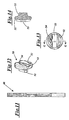
- Figures 1-5 and 8-11 show the structure of the kinematic coupling plate in greater detail.
- This plate- is secured to wall 20 by a plurality of mounting posts 42 (see figure 5).
- Three separate coupling grooves 44, 45 and 46 are formed into the kinematic coupling plate 40. These grooves are designed to mate with posts on the processing equipment (not shown) to align the access opening 8 with a port on the processing equipment.
- the grooves 44, 45 and 46 are Y-shaped to include a narrow, deeper, center channel 47 and wider, less deep, upper channel 48 which serves to catch and direct the alignment post of the processing equipment into the center channel 47 to achieve proper alignment. Proper alignment results when the three alignment posts on the processing equipment (not shown) mate with the center channel 47 of the grooves 44, 45 and 46.
- the kinematic coupling plate 40 is made of a conductive material. It is also designed to include a pair of screw receiving members 49. As explained below, members 49 each receive a screw which is used to electrically couple the kinematic coupling plate 40 to the wafer supports 60 located inside the container. This electrical coupling creates a path by which the wafer supports can be grounded to dissipate any electrical charge on the wafers or wafer supports and, thus, prevent damage to the wafers caused by static electricity.
- Figure 1 also shows a pair of handles 50. These handles are located at the center of gravity of the container. The handles are ergonomically designed so they are easily gripped from a variety of angles by the human hand. The design of the handles 50 allows them to be effectively grasped by robotic handling equipment.
- each handle 50 includes a support column 51 which joins the handle 50 to the shell 10 and a wider gripping member 52.
- the gripping member 52 has an exterior shape which permits it to be comfortably grasped by a human hand.
- the gripping member 52 also has a recessed channel formed in its end.
- Channel 53 is generally straight, but includes a notch 54.
- the channel 53 and notch 54 are present to be engaged by gripping members of a robotic arm.
- the container is designed for easy, efficient and safe handling by humans or robots.
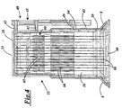
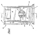
- Figures 3, 4 and 6 show some of the interior structure of the shell 10 not visible in figure 1.
- figures 3 and 4 show wafer supports 60 and 62 which cooperate to hold up to thirteen wafers 80. Typically, twelve of the wafers 80 are product wafers and one is a test wafer.
- the wafer supports 60 and 62 are all made of a material which is electrically conductive and resistant to high temperatures.
- the wafer supports 60 and 62 as shown, each have fourteen wafer dividers 65.
- a wafer edge receiving channel 66 is formed between each pair of dividers 65.
- the channels on wafer support 60 cooperate with the channels on wafer support 62 to hold the wafers 80 in a parallel spaced apart registration as shown in figures 3 and 4.
- the wafer supports 60 and 62 can be modified to hold more wafers (for example, 25) or fewer wafers (for example, 7) without deviating from the present invention.
- the wafer supports 60 and 62 could also be dimensioned to retain something other than a wafer or to retain wafers of differing sizes.
- each of the channels 66 is especially formed to retain 300mm wafers.
- the back side of each channel is curved in the circumferential direction (e.g. the direction of the circumference of the wafer 80) and in the transverse direction (e.g., the direction across the thickness of the wafer 80).
- the curvature of the backside of each channel 66 is approximately the same radius of curvature as the outside edge of the 300mm wafers 80, in both the circumferential and transverse directions. Providing the same radius of curvature along the circumferential direction presents contact between the channel's back side and the edge of the wafer 80 along an arc rather than merely at a point.
- the wafer dividers have a continuously varying slope such that gravity helps center the wafer 80 in the middle of the carrier.
- the wafer With this style of wafer divider 65, the wafer always rests on a portion of the wafer divider that has a finite slope, so edge contact is guaranteed. Further, if for any reason the wafer is moved off of dead center, one edge is raised more quickly than the other edge is lowered. Thus, for carriers where the wafers are transported horizontally, gravity may be used to help center the wafer with this support. Once centered, the wafer's vertical location is precisely defined. As the carrier is moved from one location to the next, small levels of vibration may help to center the wafer in the carrier, thus improving the horizontal positional accuracy of the wafers as well as the vertical positional accuracy.
- the divider 65 presents an area of interference for the wafer 80 as it is inserted into and removed from the carrier. Thin dividers are preferred because there is less chance of a wafer 80 hitting the divider and causing particles to be generated. On the other hand, the divider 65 must be thick enough to support the wafer 80 and to avoid deflection over the life of the container. In light of these conflicting requirements, the divider design has a continuously varying angle as shown in Figure 17.
- a pair of screws 64 are provided.
- One of the screws 64 is used to form a conductive path between the wafer support 60 and the conductive kinematic coupling plate 40.
- the other screw 64 is used to provide a conductive path between wafer support 62 and the kinematic coupling plate 40.
- This arrangement provides the advantage of grounding the wafer supports 60 and 62 via screws 64 and the kinematic coupling plate 40 so that the wafer supports 60 and 62 have no electrical charge.
- the walls of the shell 10 are not grounded and have a slightly negative charge which will cause particles in the container to migrate and attach themselves to the walls of the container where they can do no harm to the wafers. So that the screws 64 do not ground the exterior shell 10, it may be desirable to line the bores in the shell 10 through which the screws 64 pass with an insulative material.
- a door 90 is provided.
- the door 90 is shaped and dimensioned to fit within the door frame 6.
- the door engages the door frame 6 to seal the container.
- the outer edge of door frame 6 can be used to form a seal around the access opening 8 between the door frame 6 and the port of a tool used to process semiconductor wafers 80. The risk of contamination is reduced if such a seal is created before the door 90 is opened.
- the door 90 can safely be opened so that the wafers 80 can be withdrawn from the shell 10, through the port and into the tool for processing without substantial risk of contamination.
- a plurality of latches (not shown) to hold the door in the closed position will be provided.
- a flexible gasket or ring can be provided between the door 90 and frame 6 to ensure complete sealing between the door 90 and frame 6.
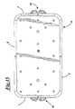
- the door 90 can be provided with a wafer cushion 92.
- cushion 92 has a pair of rigid rails 93 and 94 and a plurality of deformable cross-members 95. Thirteen deformable cross-members 95 are shown in figure 16.
- Each cross-member 95 has a pair of dividers 96. Each divider 96 is aligned with a divider 97 on rigid rail 93 and a divider 98 on rigid rail 94.
- Cross-members 95 will deform until the edges of wafers 80 also engage the rigid rails 93 and 94. Even if the wafers 80 are jarred during transport, contact with and support by cushion 92 is not lost because of the deformable cross-members 95.
- a wafer cushion 92 on the door 90 yields three areas of support for the wafers 80, thereby reducing movement and vibration of the wafers 80 during transport. Supporting the wafers 80 in three areas reduces damage to the wafers due to scraping, rubbing or impacting surfaces within the container. It also limits generation of particles due to such scraping, rubbing or impacting.
- means can be provided on the exterior door for kinematically coupling the door 90 to another surface. This can be a series of three grooves (not shown) similar to those shown in kinematic coupling plate 40 which mate with projections on the surface or three projections on the door 90 which mate with grooves on the surface.
- the present invention has been illustrated and described with reference to the preferred embodiment thereof, the invention may also be used in conjunction with the transport and storage of liquid crystal displays, flat panel displays, photomasks, rigid memory disks, substrates, and the like.
- various components of the invention may be constructed so that they are removable and replaceable to extend the life of the container. This is certainly true of the wafer supports 60 and 62 and wafer cushion 92 which can be removed and replaced with supports or cushions more ideally suited for other items to be held in the container. It should be understood, therefore, that the illustrations and descriptions provided herein are not intended to be limiting and that numerous modifications can be made within the scope of this invention and the claims set forth below.
Landscapes
- Engineering & Computer Science (AREA)
- Mechanical Engineering (AREA)
- Packaging Frangible Articles (AREA)
- Container, Conveyance, Adherence, Positioning, Of Wafer (AREA)
Claims (14)
- Behälter zum Erzeugen einer Mikro-Umgebung, welche darin aufgenommene Gegenstände vor Beschädigung schützt, wobei der Behälter von dem Typ mit einer Hülle (10) mit einer Öffnung (8) zum Einführen und Herausnehmen von Gegenständen in die/aus der Hülle ist', wobei der Behälter ein Paar Halterungen (60,62), die zusammenwirken, um mehrere in dem Behälter aufgenommene Gegenstände (80) in einer parallelen, beabstandeten Position in bezug aufeinander festzuhalten, und eine Tür (90) zum Abdichten der Öffnung der Hülle aufweist, wobei der Behälter ferner dadurch gekennzeichnet ist, daß die Hülle aus einem Material gefertigt ist, welches inhärent eine geringfügig negative elektrische Ladung besitzt, und daß ein Mittel (64) zum Erzeugen eines elektrischen Pfads vorgesehen ist, durch den die Halterungen geerdet sind, so daß Teilchen innerhalb der Hülle (10) von den Gegenständen (80) und den Halterungen (60,62) weg und zur Hülle des Behälters hin gezogen werden.
- Behälter nach Anspruch 1, wobei die im Behälter aufgenommenen Gegenstände Halbleiter-Wafer (80) sind.
- Behälter nach Anspruch 1, ferner mit einem Paar Handgriffen (50), die an gegenüberliegenden Seiten des Schwerkraftzentrums des Behälters gelegen sind.
- Behälter nach Anspruch 3, wobei jeder der Handgriffe (50) eine Nut bzw. Rille mit einer Ausrichtungskerbe (53,54) aufweist, so daß der Handgriff sicher von einen Roboter ergriffen werden kann.
- Behälter nach Anspruch 1, ferner mit einer kinematischen Kopplungsplatte (40), die durch mehrere Zapfen an der Außenseite der Hülle gesichert ist, wobei die kinematische Kopplungsplatte drei Ausrichtungsnuten (44, 45, 46) aufweist, wobei jede der Ausrichtungsnuten einen im allgemeinen Y-förmigen Querschnitt hat.
- Behälter nach Anspruch 5, wobei die Ausrichtungsnuten (44,45,46) der kinematischen Kopplungsplatte (40) dazu verwendet werden, die Behältertür (90) mit der Anschlußöffnung eines zum Bearbeiten von Halbleiter-Wafern verwendeten Werkzeugs auszurichten, so daß um die Öffnung der Hülle und die Anschlußöffnung des Werkzeugs eine Dichtung erzeugt wird, bevor die Behältertür geöffnet wird und die Wafer aus der Hülle durch die Anschlußöffnung in das Werkzeug zur Bearbeitung abgezogen werden.
- Behälter nach Anspruch 1, ferner mit einer kinematischen Kopplungsplatte (40), die an der Außenseite der Hülle gesichert ist, wobei die kinematische Kopplungsplatte aus einem elektrisch leitenden Material gefertigt ist.
- Behälter nach Anspruch 7, wobei das Mittel (64) zum Erzeugen eines elektrischen Pfads, durch den die Halterungen geerdet sind, eine elektrisch leitende Verbindung zwischen jeder der Halterungen (60,62) und der kinematischen Kopplungsplatte (40) umfaßt.
- Behälter nach Anspruch 1, wobei die Tür (90) ein Mittel an ihrer Außenfläche zum Koppeln der Tür mit einer anderen Oberfläche aufweist.
- Behälter nach Anspruch 1, wobei jede der Halterungen (60, 62) lösbar an der Hülle gesichert ist, so daß solche Halterungen zur Reinigung oder zum Austausch entfernt werden können.
- Behälter nach Anspruch 2, wobei die Halterungen (60,62) mehrere Kanäle (66) aufweisen, wobei jeder der Kanäle eine Rückseite hat, die in der Umfangsrichtung gekrümmt ist.
- Behälter nach Anspruch 11, wobei der Krümmungsradius der Rückseite der Kanäle (66) in der Umfangsrichtung im allgemeinen der gleiche ist wie der Krümmungsradius in der Umfangsrichtung der Wafer.
- Behälter nach Anspruch 2, wobei jede des Paars Halterungen (60,62) mehrere Wafer-Unterteiler (65) aufweist, und jeder der Wafer-Unterteiler eine kontinuierlich variierende Neigung hat, um einen der Halbleiter-Wafer haltern zu helfen.
- Behälter zum Erzeugen einer Mikroumgebung, welche darin aufgenommene Halbleiter-Wafer (80) vor Beschädigung schützt, wobei der Behälter von dem Typ mit einer Kunststoffhülle (10) mit einer vorderen Öffnung (8) zum Einführen und Herausnehmen von Halbleiter-Wafern in die bzw. aus der Hülle aufweist, wobei der Behälter ein Paar am Inneren der Hülle angebrachte Halterungen (60,62), welche zusammenwirken, um mehrere im Behälter in einer parallelen, beabstandeten Position in bezug aufeinander aufgenommene Halbleiter-Wafer (80) zu halten, sowie eine Tür (90) zum Abdichten der Öffnung der Hülle aufweist, wobei der Behälter ferner dadurch gekennzeichnet ist, daß die Kunststoffhülle inhärent eine geringfügig negative elektrische Ladung besitzt und ein Mittel (64) zum Erzeugen eines elektrischen Pfads vorhanden ist, durch das/den die Halterungen geerdet sind, so daß Teilchen innerhalb der Hülle (10) von den Halbleiter-Wafern (80) und den Halterungen weg zur Hülle des Behälters hin gezogen werden.
Applications Claiming Priority (1)
| Application Number | Priority Date | Filing Date | Title |
|---|---|---|---|
| PCT/US1995/012516 WO1997013710A1 (en) | 1995-10-13 | 1995-10-13 | 300mm MICROENVIRONMENT POD WITH DOOR ON SIDE |
Publications (3)
| Publication Number | Publication Date |
|---|---|
| EP0857150A1 EP0857150A1 (de) | 1998-08-12 |
| EP0857150A4 EP0857150A4 (de) | 1999-04-14 |
| EP0857150B1 true EP0857150B1 (de) | 2002-03-27 |
Family
ID=22249868
Family Applications (1)
| Application Number | Title | Priority Date | Filing Date |
|---|---|---|---|
| EP95935679A Expired - Lifetime EP0857150B1 (de) | 1995-10-13 | 1995-10-13 | 300 mm behälter mit mikroumgebung und seitentür und erdungsleitung |
Country Status (8)
| Country | Link |
|---|---|
| US (4) | USRE38221E1 (de) |
| EP (1) | EP0857150B1 (de) |
| JP (1) | JP3483573B2 (de) |
| KR (1) | KR100428827B1 (de) |
| CA (1) | CA2218260C (de) |
| DE (1) | DE69526126T2 (de) |
| TW (1) | TW278312B (de) |
| WO (1) | WO1997013710A1 (de) |
Cited By (1)
| Publication number | Priority date | Publication date | Assignee | Title |
|---|---|---|---|---|
| US7422107B2 (en) | 2006-01-25 | 2008-09-09 | Entegris, Inc. | Kinematic coupling with textured contact surfaces |
Families Citing this family (34)
| Publication number | Priority date | Publication date | Assignee | Title |
|---|---|---|---|---|
| JP3483573B2 (ja) | 1995-10-13 | 2004-01-06 | エムパック インコーポレイテッド | パッケージ |
| US6010008A (en) * | 1997-07-11 | 2000-01-04 | Fluoroware, Inc. | Transport module |
| US6736268B2 (en) * | 1997-07-11 | 2004-05-18 | Entegris, Inc. | Transport module |
| KR100460309B1 (ko) * | 1998-02-06 | 2004-12-04 | 미라이얼 가부시키가이샤 | 박판지지용기 |
| US6808668B2 (en) | 1998-05-28 | 2004-10-26 | Entegris, Inc. | Process for fabricating composite substrate carrier |
| US6871741B2 (en) | 1998-05-28 | 2005-03-29 | Entegris, Inc. | Composite substrate carrier |
| US6216874B1 (en) * | 1998-07-10 | 2001-04-17 | Fluoroware, Inc. | Wafer carrier having a low tolerance build-up |
| TW437723U (en) | 2000-06-16 | 2001-05-28 | Ind Tech Res Inst | Wafer box with foldable handle |
| EP1339622A4 (de) * | 2000-12-04 | 2006-03-08 | Entegris Inc | Waferträger mit stapeladapterplatte |
| US20020090282A1 (en) * | 2001-01-05 | 2002-07-11 | Applied Materials, Inc. | Actuatable loadport system |
| KR100876626B1 (ko) * | 2001-04-01 | 2008-12-31 | 인티그리스, 인코포레이티드 | 박형 웨이퍼 인서트 |
| US6923325B2 (en) | 2001-07-12 | 2005-08-02 | Entegris, Inc. | Horizontal cassette |
| KR20040035739A (ko) * | 2001-08-27 | 2004-04-29 | 엔테그리스, 아이엔씨. | 반도체 웨이퍼 디스크 및 유사 재고품용 모듈형 캐리어 |
| US6951284B2 (en) * | 2001-11-14 | 2005-10-04 | Entegris, Inc. | Wafer carrier with wafer retaining system |
| US20030188990A1 (en) * | 2001-11-14 | 2003-10-09 | Bhatt Sanjiv M. | Composite kinematic coupling |
| JP4329541B2 (ja) * | 2001-11-27 | 2009-09-09 | インテグリス・インコーポレーテッド | ドアにより機能化されるアース経路を有した前方開閉型ウエハーキャリア及びウエハーキャリアのドアを経由したアース経路を設ける方法 |
| USD479399S1 (en) | 2001-12-03 | 2003-09-09 | Ebara Corporation | Container for transporting substrates |
| USD491725S1 (en) | 2001-12-19 | 2004-06-22 | Ebara Corporation | Container for transporting substrates |
| US7175026B2 (en) | 2002-05-03 | 2007-02-13 | Maxtor Corporation | Memory disk shipping container with improved contaminant control |
| US20040074808A1 (en) * | 2002-07-05 | 2004-04-22 | Entegris, Inc. | Fire retardant wafer carrier |
| WO2004036384A2 (en) * | 2002-10-18 | 2004-04-29 | Intellocity Usa, Inc. | Ichoose video advertising |
| TWI283621B (en) | 2002-12-02 | 2007-07-11 | Miraial Co Ltd | Thin plate storage container |
| US7145157B2 (en) * | 2003-09-11 | 2006-12-05 | Applied Materials, Inc. | Kinematic ion implanter electrode mounting |
| US7182203B2 (en) * | 2003-11-07 | 2007-02-27 | Entegris, Inc. | Wafer container and door with vibration dampening latching mechanism |
| US7252199B2 (en) * | 2004-03-26 | 2007-08-07 | Entegris, Inc. | Disk cassette system |
| US7528936B2 (en) * | 2005-02-27 | 2009-05-05 | Entegris, Inc. | Substrate container with pressure equalization |
| JP4668133B2 (ja) * | 2006-06-28 | 2011-04-13 | 三甲株式会社 | ウエハ容器の位置決め構造 |
| WO2008008270A2 (en) * | 2006-07-07 | 2008-01-17 | Entegris, Inc. | Wafer cassette |
| US20080157455A1 (en) * | 2006-12-29 | 2008-07-03 | Applied Materials, Inc. | Compliant substrate holding assembly |
| TWM336941U (en) * | 2007-11-15 | 2008-07-21 | Gudeng Prec Ind Co Ltd | Storage apparatus for storing semiconductor element or reticle |
| US20120298549A1 (en) | 2010-02-19 | 2012-11-29 | Shin-Etsu Polymer Co., Ltd. | Substrate storage container |
| CN103765569A (zh) | 2011-05-03 | 2014-04-30 | 恩特格里公司 | 具有粒子罩的晶片容器 |
| CN105993067B (zh) | 2013-04-26 | 2019-04-16 | 恩特格里斯公司 | 用于大直径晶片的具有锁止机构的晶片容器 |
| NL2022185B1 (nl) * | 2018-12-12 | 2020-07-02 | Suss Microtec Lithography Gmbh | Substratkassette |
Citations (2)
| Publication number | Priority date | Publication date | Assignee | Title |
|---|---|---|---|---|
| US5273159A (en) * | 1992-05-26 | 1993-12-28 | Empak, Inc. | Wafer suspension box |
| US5423422A (en) * | 1994-03-14 | 1995-06-13 | Empak, Inc. | Flat panel display container |
Family Cites Families (47)
| Publication number | Priority date | Publication date | Assignee | Title |
|---|---|---|---|---|
| US4043451A (en) | 1976-03-18 | 1977-08-23 | Fluoroware, Inc. | Shipping container for silicone semiconductor wafers |
| JPS57113446A (en) | 1980-12-29 | 1982-07-14 | Sony Corp | Cassette tape recorder |
| US4450960A (en) | 1982-08-30 | 1984-05-29 | Empak Inc. | Package |
| US4520925A (en) | 1983-08-09 | 1985-06-04 | Empak Inc. | Package |
| US4557382A (en) * | 1983-08-17 | 1985-12-10 | Empak Inc. | Disk package |
| JPS60173826A (ja) | 1984-02-20 | 1985-09-07 | Shin Etsu Handotai Co Ltd | 輸送用ウエハ−ケ−ス |
| CA1196372A (en) | 1984-05-07 | 1985-11-05 | Will B. Robinson | Anti-static transit case |
| JPS6233436A (ja) | 1985-08-07 | 1987-02-13 | Shin Etsu Handotai Co Ltd | 輸送用ウエ−ハケ−ス |
| JPS6283486A (ja) | 1985-10-09 | 1987-04-16 | Seiko Epson Corp | ニツケル電鋳メツキ液組成 |
| JPS6287443A (ja) | 1985-10-09 | 1987-04-21 | 日本磁力選鉱株式会社 | 製鋼スラグの処理方法 |
| JPH0637818B2 (ja) | 1985-10-26 | 1994-05-18 | 株式会社ユ−シン | ドアハンドル装置 |
| US4739882A (en) * | 1986-02-13 | 1988-04-26 | Asyst Technologies | Container having disposable liners |
| JPS62212319A (ja) | 1986-03-13 | 1987-09-18 | Nippon Kaihatsu Consultant:Kk | 鉱物質を含浸した薬草浴剤とその製法 |
| US4721207A (en) * | 1986-04-28 | 1988-01-26 | Tensho Electric Industrial Co., Ltd. | Hard disk container |
| JPS6349387A (ja) | 1986-08-15 | 1988-03-02 | Kawasaki Steel Corp | レ−ザ−加工装置 |
| US4747488A (en) | 1986-12-01 | 1988-05-31 | Shoji Kikuchi | Hard disk container |
| JPS6413717A (en) | 1987-07-08 | 1989-01-18 | Nec Corp | Wafer carrier |
| JPS6437047A (en) | 1987-07-31 | 1989-02-07 | Hitachi Ltd | Semiconductor device |
| JPH0231789A (ja) | 1988-07-22 | 1990-02-01 | Janome Sewing Mach Co Ltd | 電子ミシン |
| JPH03129719A (ja) | 1989-05-17 | 1991-06-03 | Fujitsu Ltd | 半導体装置の製造方法 |
| JP2816864B2 (ja) * | 1989-07-07 | 1998-10-27 | 大塚化学株式会社 | 搬送用ウエーハバスケット及び収納ケース |
| US5253755A (en) | 1991-03-20 | 1993-10-19 | Fluoroware, Inc. | Cushioned cover for disk container |
| US5228568A (en) | 1991-08-30 | 1993-07-20 | Shin-Etsu Handotai Co., Ltd. | Semiconductor wafer basket |
| JPH0563066A (ja) | 1991-08-30 | 1993-03-12 | Shin Etsu Handotai Co Ltd | ウエーハ収納容器の係止構造 |
| JPH05218185A (ja) | 1992-02-06 | 1993-08-27 | Nippon Steel Corp | ウェハキャリアボックス |
| US5255797A (en) | 1992-02-26 | 1993-10-26 | Fluoroware, Inc. | Wafer carrier with wafer retaining cushions |
| JPH05254582A (ja) | 1992-03-06 | 1993-10-05 | Nippon Steel Corp | ウェハキャリア及びキャリアボックス |
| US5469963A (en) * | 1992-04-08 | 1995-11-28 | Asyst Technologies, Inc. | Sealable transportable container having improved liner |
| US5555981A (en) | 1992-05-26 | 1996-09-17 | Empak, Inc. | Wafer suspension box |
| JP2513110B2 (ja) * | 1992-09-07 | 1996-07-03 | 凸版印刷株式会社 | フォトマスク用容器 |
| JPH06283486A (ja) | 1993-03-30 | 1994-10-07 | Dainippon Screen Mfg Co Ltd | ウエハ保持装置及びウエハ収納カセット |
| JP2552625B2 (ja) | 1993-11-09 | 1996-11-13 | 淀川化成株式会社 | ガラス基板搬送用ボックス |
| US5472086A (en) | 1994-03-11 | 1995-12-05 | Holliday; James E. | Enclosed sealable purgible semiconductor wafer holder |
| US5476176A (en) | 1994-05-23 | 1995-12-19 | Empak, Inc. | Reinforced semiconductor wafer holder |
| US5482161A (en) | 1994-05-24 | 1996-01-09 | Fluoroware, Inc. | Mechanical interface wafer container |
| US5586658A (en) | 1995-06-06 | 1996-12-24 | Fluoroware, Inc. | Wafer cushions for wafer shipper |
| JP3145252B2 (ja) | 1994-07-29 | 2001-03-12 | 淀川化成株式会社 | 基板支承用側板およびそれを用いたカセット |
| TW273635B (de) * | 1994-09-01 | 1996-04-01 | Aesop | |
| US5982182A (en) | 1994-09-01 | 1999-11-09 | Chiu; Michael A. | Interface apparatus for automatic test equipment with positioning modules incorporating kinematic surfaces |
| US5785186A (en) | 1994-10-11 | 1998-07-28 | Progressive System Technologies, Inc. | Substrate housing and docking system |
| JPH09107026A (ja) | 1995-10-12 | 1997-04-22 | Shin Etsu Polymer Co Ltd | ウェーハ収納容器のウェーハカセット |
| JP3483573B2 (ja) | 1995-10-13 | 2004-01-06 | エムパック インコーポレイテッド | パッケージ |
| US6003674A (en) | 1996-05-13 | 1999-12-21 | Brooks; Ray Gene | Method and apparatus for packing contaminant-sensitive articles and resulting package |
| US5915562A (en) | 1996-07-12 | 1999-06-29 | Fluoroware, Inc. | Transport module with latching door |
| US5711427A (en) | 1996-07-12 | 1998-01-27 | Fluoroware, Inc. | Wafer carrier with door |
| US5788082A (en) | 1996-07-12 | 1998-08-04 | Fluoroware, Inc. | Wafer carrier |
| US6082540A (en) | 1999-01-06 | 2000-07-04 | Fluoroware, Inc. | Cushion system for wafer carriers |
-
1995
- 1995-10-13 JP JP51500597A patent/JP3483573B2/ja not_active Expired - Lifetime
- 1995-10-13 US US09/943,098 patent/USRE38221E1/en not_active Expired - Lifetime
- 1995-10-13 DE DE69526126T patent/DE69526126T2/de not_active Expired - Lifetime
- 1995-10-13 US US11/351,214 patent/USRE42402E1/en not_active Expired - Lifetime
- 1995-10-13 EP EP95935679A patent/EP0857150B1/de not_active Expired - Lifetime
- 1995-10-13 US US08/913,260 patent/US5944194A/en not_active Ceased
- 1995-10-13 WO PCT/US1995/012516 patent/WO1997013710A1/en not_active Ceased
- 1995-10-13 US US10/310,069 patent/USRE41231E1/en not_active Expired - Lifetime
- 1995-10-13 KR KR1019970707189A patent/KR100428827B1/ko not_active Expired - Fee Related
- 1995-10-13 CA CA002218260A patent/CA2218260C/en not_active Expired - Fee Related
- 1995-10-20 TW TW084111084A patent/TW278312B/zh not_active IP Right Cessation
Patent Citations (2)
| Publication number | Priority date | Publication date | Assignee | Title |
|---|---|---|---|---|
| US5273159A (en) * | 1992-05-26 | 1993-12-28 | Empak, Inc. | Wafer suspension box |
| US5423422A (en) * | 1994-03-14 | 1995-06-13 | Empak, Inc. | Flat panel display container |
Cited By (1)
| Publication number | Priority date | Publication date | Assignee | Title |
|---|---|---|---|---|
| US7422107B2 (en) | 2006-01-25 | 2008-09-09 | Entegris, Inc. | Kinematic coupling with textured contact surfaces |
Also Published As
| Publication number | Publication date |
|---|---|
| CA2218260C (en) | 2006-05-23 |
| HK1017325A1 (en) | 1999-11-19 |
| USRE41231E1 (en) | 2010-04-20 |
| EP0857150A4 (de) | 1999-04-14 |
| DE69526126T2 (de) | 2002-11-07 |
| WO1997013710A1 (en) | 1997-04-17 |
| DE69526126D1 (de) | 2002-05-02 |
| USRE42402E1 (en) | 2011-05-31 |
| TW278312B (en) | 1996-06-11 |
| US5944194A (en) | 1999-08-31 |
| EP0857150A1 (de) | 1998-08-12 |
| KR100428827B1 (ko) | 2005-04-20 |
| JPH11513347A (ja) | 1999-11-16 |
| CA2218260A1 (en) | 1997-04-17 |
| KR19980703789A (ko) | 1998-12-05 |
| USRE38221E1 (en) | 2003-08-19 |
| JP3483573B2 (ja) | 2004-01-06 |
Similar Documents
| Publication | Publication Date | Title |
|---|---|---|
| USRE42402E1 (en) | 300 mm microenvironment pod with door on side | |
| NL1009466C2 (nl) | Transportmoduul voor wafels. | |
| TWI469901B (zh) | 晶圓容置箱及其製造方法 | |
| US4966284A (en) | Substrate package | |
| US7347329B2 (en) | Substrate carrier | |
| EP2537780B1 (de) | Substratspeicherbehälter | |
| CN1478293A (zh) | 带有叠置适配器板的晶片搬运器 | |
| EP0343762A2 (de) | Verpackung für Halbleiterscheiben | |
| CN1071259C (zh) | 侧面有门的300毫米微环境舱 | |
| KR100428828B1 (ko) | 300㎜적재컨테이너 | |
| KR980009066A (ko) | 반도체 기판 캐리어 이송 및 사용 방법 및 장치 | |
| HK1017325B (en) | 300mm microenvironment pod with door on side | |
| CN223990300U (zh) | 面板收纳容器及清洁系统 | |
| CN1897851A (zh) | 基板容器 | |
| WO2008024388A2 (en) | Substrate container with outboard kinematic coupling structure |
Legal Events
| Date | Code | Title | Description |
|---|---|---|---|
| PUAI | Public reference made under article 153(3) epc to a published international application that has entered the european phase |
Free format text: ORIGINAL CODE: 0009012 |
|
| 17P | Request for examination filed |
Effective date: 19971024 |
|
| AK | Designated contracting states |
Kind code of ref document: A1 Designated state(s): DE |
|
| A4 | Supplementary search report drawn up and despatched |
Effective date: 19990226 |
|
| AK | Designated contracting states |
Kind code of ref document: A4 Designated state(s): DE |
|
| 17Q | First examination report despatched |
Effective date: 20000105 |
|
| RTI1 | Title (correction) |
Free format text: 300 MM MICROENVIRONMENT POD WITH DOOR ON SIDE AND GROUNDING ELECTRICAL PATH |
|
| GRAG | Despatch of communication of intention to grant |
Free format text: ORIGINAL CODE: EPIDOS AGRA |
|
| GRAG | Despatch of communication of intention to grant |
Free format text: ORIGINAL CODE: EPIDOS AGRA |
|
| GRAH | Despatch of communication of intention to grant a patent |
Free format text: ORIGINAL CODE: EPIDOS IGRA |
|
| GRAH | Despatch of communication of intention to grant a patent |
Free format text: ORIGINAL CODE: EPIDOS IGRA |
|
| GRAA | (expected) grant |
Free format text: ORIGINAL CODE: 0009210 |
|
| AK | Designated contracting states |
Kind code of ref document: B1 Designated state(s): DE |
|
| REF | Corresponds to: |
Ref document number: 69526126 Country of ref document: DE Date of ref document: 20020502 |
|
| PLBE | No opposition filed within time limit |
Free format text: ORIGINAL CODE: 0009261 |
|
| STAA | Information on the status of an ep patent application or granted ep patent |
Free format text: STATUS: NO OPPOSITION FILED WITHIN TIME LIMIT |
|
| 26N | No opposition filed |
Effective date: 20021230 |
|
| PGFP | Annual fee paid to national office [announced via postgrant information from national office to epo] |
Ref country code: DE Payment date: 20141007 Year of fee payment: 20 |
|
| REG | Reference to a national code |
Ref country code: DE Ref legal event code: R071 Ref document number: 69526126 Country of ref document: DE |