WO2022201283A1 - ストレージシステム - Google Patents
ストレージシステム Download PDFInfo
- Publication number
- WO2022201283A1 WO2022201283A1 PCT/JP2021/011856 JP2021011856W WO2022201283A1 WO 2022201283 A1 WO2022201283 A1 WO 2022201283A1 JP 2021011856 W JP2021011856 W JP 2021011856W WO 2022201283 A1 WO2022201283 A1 WO 2022201283A1
- Authority
- WO
- WIPO (PCT)
- Prior art keywords
- wafer
- cassette
- stocker
- wafer cassette
- semiconductor
- Prior art date
- Legal status (The legal status is an assumption and is not a legal conclusion. Google has not performed a legal analysis and makes no representation as to the accuracy of the status listed.)
- Ceased
Links
Images

















Classifications
-
- H—ELECTRICITY
- H10—SEMICONDUCTOR DEVICES; ELECTRIC SOLID-STATE DEVICES NOT OTHERWISE PROVIDED FOR
- H10P—GENERIC PROCESSES OR APPARATUS FOR THE MANUFACTURE OR TREATMENT OF DEVICES COVERED BY CLASS H10
- H10P72/00—Handling or holding of wafers, substrates or devices during manufacture or treatment thereof
- H10P72/30—Handling or holding of wafers, substrates or devices during manufacture or treatment thereof for conveying, e.g. between different workstations
- H10P72/34—Handling or holding of wafers, substrates or devices during manufacture or treatment thereof for conveying, e.g. between different workstations the wafers being stored in a carrier, involving loading and unloading
- H10P72/3411—Handling or holding of wafers, substrates or devices during manufacture or treatment thereof for conveying, e.g. between different workstations the wafers being stored in a carrier, involving loading and unloading involving loading and unloading of wafers
- H10P72/3412—Batch transfer of wafers
-
- G—PHYSICS
- G06—COMPUTING OR CALCULATING; COUNTING
- G06F—ELECTRIC DIGITAL DATA PROCESSING
- G06F12/00—Accessing, addressing or allocating within memory systems or architectures
-
- G—PHYSICS
- G06—COMPUTING OR CALCULATING; COUNTING
- G06F—ELECTRIC DIGITAL DATA PROCESSING
- G06F12/00—Accessing, addressing or allocating within memory systems or architectures
- G06F12/02—Addressing or allocation; Relocation
- G06F12/06—Addressing a physical block of locations, e.g. base addressing, module addressing, memory dedication
-
- G—PHYSICS
- G11—INFORMATION STORAGE
- G11C—STATIC STORES
- G11C5/00—Details of stores covered by group G11C11/00
- G11C5/02—Disposition of storage elements, e.g. in the form of a matrix array
- G11C5/04—Supports for storage elements, e.g. memory modules; Mounting or fixing of storage elements on such supports
-
- G—PHYSICS
- G11—INFORMATION STORAGE
- G11C—STATIC STORES
- G11C7/00—Arrangements for writing information into, or reading information out from, a digital store
- G11C7/04—Arrangements for writing information into, or reading information out from, a digital store with means for avoiding disturbances due to temperature effects
-
- H—ELECTRICITY
- H10—SEMICONDUCTOR DEVICES; ELECTRIC SOLID-STATE DEVICES NOT OTHERWISE PROVIDED FOR
- H10P—GENERIC PROCESSES OR APPARATUS FOR THE MANUFACTURE OR TREATMENT OF DEVICES COVERED BY CLASS H10
- H10P72/00—Handling or holding of wafers, substrates or devices during manufacture or treatment thereof
- H10P72/30—Handling or holding of wafers, substrates or devices during manufacture or treatment thereof for conveying, e.g. between different workstations
- H10P72/32—Handling or holding of wafers, substrates or devices during manufacture or treatment thereof for conveying, e.g. between different workstations between different workstations
- H10P72/3218—Conveying cassettes, containers or carriers
-
- H—ELECTRICITY
- H10—SEMICONDUCTOR DEVICES; ELECTRIC SOLID-STATE DEVICES NOT OTHERWISE PROVIDED FOR
- H10P—GENERIC PROCESSES OR APPARATUS FOR THE MANUFACTURE OR TREATMENT OF DEVICES COVERED BY CLASS H10
- H10P72/00—Handling or holding of wafers, substrates or devices during manufacture or treatment thereof
- H10P72/30—Handling or holding of wafers, substrates or devices during manufacture or treatment thereof for conveying, e.g. between different workstations
- H10P72/34—Handling or holding of wafers, substrates or devices during manufacture or treatment thereof for conveying, e.g. between different workstations the wafers being stored in a carrier, involving loading and unloading
- H10P72/3402—Mechanical parts of transfer devices
-
- H—ELECTRICITY
- H10—SEMICONDUCTOR DEVICES; ELECTRIC SOLID-STATE DEVICES NOT OTHERWISE PROVIDED FOR
- H10P—GENERIC PROCESSES OR APPARATUS FOR THE MANUFACTURE OR TREATMENT OF DEVICES COVERED BY CLASS H10
- H10P72/00—Handling or holding of wafers, substrates or devices during manufacture or treatment thereof
- H10P72/30—Handling or holding of wafers, substrates or devices during manufacture or treatment thereof for conveying, e.g. between different workstations
- H10P72/34—Handling or holding of wafers, substrates or devices during manufacture or treatment thereof for conveying, e.g. between different workstations the wafers being stored in a carrier, involving loading and unloading
- H10P72/3404—Storage means
-
- H—ELECTRICITY
- H10—SEMICONDUCTOR DEVICES; ELECTRIC SOLID-STATE DEVICES NOT OTHERWISE PROVIDED FOR
- H10P—GENERIC PROCESSES OR APPARATUS FOR THE MANUFACTURE OR TREATMENT OF DEVICES COVERED BY CLASS H10
- H10P72/00—Handling or holding of wafers, substrates or devices during manufacture or treatment thereof
- H10P72/50—Handling or holding of wafers, substrates or devices during manufacture or treatment thereof for positioning, orientation or alignment
Definitions
- Embodiments of the present invention relate to technology for controlling nonvolatile memory.
- SSD solid state drive
- SSDs are used as storage for various computers. Recently, SSDs are also used as storage in data centers.
- a problem to be solved by one embodiment of the present invention is to provide a storage system useful for processing large amounts of data.
- the storage system includes a wafer stocker, a cassette, a wafer cassette stocker, a host device, a wafer transfer device, and a wafer cassette transfer device.
- the wafer stocker can store a plurality of semiconductor wafers each having a plurality of nonvolatile memory devices formed thereon.
- the cassette is configured to accommodate at least one of the plurality of semiconductor wafers within a cassette housing capable of accommodating at least one of the plurality of semiconductor wafers.
- the wafer cassette stocker can store a wafer cassette including a cassette housing and semiconductor wafers accommodated in the cassette housing.
- the host device includes at least one slot to which a wafer cassette can be connected, and is configured to read data from and write data to the semiconductor wafers contained in the wafer cassette connected to the slot.
- the wafer transport device is configured to transport semiconductor wafers between the wafer stocker and the cassette.
- a wafer cassette transfer device is adapted to transfer the wafer cassette between the cassette, the wafer cassette stocker and the host device.
- the host device determines the first semiconductor wafer to be accessed among the plurality of semiconductor wafers.
- the host device reads or writes data to or from the first semiconductor wafer when a wafer cassette to be accessed containing the first semiconductor wafer is connected to a slot of the host device.
- the host device When the wafer cassette to be accessed is not connected to the slot of the host device and is stored in the wafer cassette stocker, the host device causes the wafer cassette transfer device to move the wafer cassette to be accessed into the slot of the host device. transport and connect.
- the host device causes the wafer transfer device to transfer the first semiconductor wafer from the wafer stocker to the cassette.
- FIG. 1 is a diagram showing a configuration example of a storage system according to an embodiment
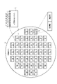
- FIG. FIG. 2 is a diagram showing a configuration example of a semiconductor wafer according to the embodiment
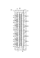
- FIG. 2 is a diagram showing a configuration example of a cassette according to the embodiment
- 1 is a diagram showing a configuration example of a host computer according to an embodiment
- FIG. FIG. 2 is a plan view showing an arrangement example of a wafer stocker, a cassette, a wafer cassette stocker, a host computer, a wafer transfer device, and a wafer cassette transfer device according to the embodiment
- the top view which shows the structural example of the wafer stocker which concerns on embodiment.
- FIG. 2 is a diagram showing a configuration example of a robot arm used as a wafer transfer device according to the embodiment
- FIG. 4 is a view showing part of the operation of transferring semiconductor wafers from the first wafer stocker to the second wafer stocker according to the embodiment
- FIG. 10 is a view showing the rest of the operation of transferring semiconductor wafers from the first wafer stocker to the second wafer stocker according to the embodiment
- FIG. 2 is a plan view showing an arrangement example of a plurality of robot arms used as a wafer transfer device and a wafer cassette transfer device according to the embodiment
- FIG. 4 is a plan view showing another arrangement example of a plurality of robot arms used as the wafer transfer device and the wafer cassette transfer device according to the embodiment;
- 1 is a diagram showing a configuration example of a host device according to an embodiment
- FIG. 1 is a block diagram showing a configuration example of a host device according to an embodiment
- FIG. 4 is a diagram for explaining an operation based on changing the priority of semiconductor wafers, which is executed in the storage system according to the embodiment
- FIG. 4 is a diagram for explaining another operation based on changing the priority of semiconductor wafers, which is executed in the storage system according to the embodiment;
- FIG. 4 is a diagram for explaining operations performed in the storage system according to the embodiment when a wafer cassette to be accessed has already been connected to a slot of a host device;
- FIG. 4 is a diagram for explaining operations performed in the storage system according to the embodiment when a wafer cassette to be accessed is stored in a wafer cassette stocker;
- FIG. 4 is a diagram for explaining operations performed in the storage system according to the embodiment when a wafer cassette to be accessed is not stored in a wafer cassette stocker;
- FIG. 5 is a diagram for explaining another operation performed in the storage system according to the embodiment when the wafer cassette to be accessed is not stored in the wafer cassette stocker;
- FIG. 4 is a diagram for explaining operations performed in the storage system according to the embodiment when a wafer cassette to be accessed has already been connected to a slot of a host device;
- FIG. 4 is a diagram for explaining operations performed in the storage system according to the embodiment when a wafer cassette to be accessed is stored in a wafer cassette
- FIG. 10 is a diagram for explaining still another operation performed in the storage system according to the embodiment when the wafer cassette to be accessed is not stored in the wafer cassette stocker;
- FIG. 10 is a diagram for explaining still another operation performed in the storage system according to the embodiment when the wafer cassette to be accessed is not stored in the wafer cassette stocker;
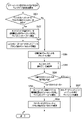
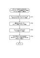
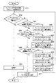
- 4 is a flowchart showing the procedure of data read or write processing executed by a host device in a storage system according to an embodiment; 4 is a flowchart showing the procedure of access processing executed by the host device according to the embodiment; 4 is a flowchart showing the procedure of wafer cassette transfer processing executed by the host device according to the embodiment; 4 is a flowchart showing the procedure of wafer cassette transfer processing executed by the host device according to the embodiment when the host device has an empty slot.
- 4 is a flowchart showing the procedure of wafer cassette transfer processing executed by the host device according to the embodiment when the host device has no empty slots.
- 4 is a flow chart showing the procedure of wafer cassette assembly or disassembly processing executed by the host device according to the embodiment when the host device has an empty slot.
- 4 is a flowchart showing the procedure of wafer cassette assembly or disassembly processing executed by the host device according to the embodiment when the host device has no empty slots.
- 4 is a flow chart showing the procedure of a wafer cassette connection error coping process executed by the host device according to the embodiment.
- 4 is a flow chart showing a procedure for processing a prohibited cassette housing, which is executed by the host device according to the embodiment; FIG.
- FIG. 4 is a diagram showing a configuration for raising the temperature of semiconductor wafers contained in the wafer cassette according to the embodiment;
- FIG. 4 is a diagram for explaining edge processing for a semiconductor wafer according to the embodiment;
- FIG. 4 is a diagram for explaining a centering arm provided in the cassette housing according to the embodiment;
- FIG. 4 is a diagram showing a rewiring layer formed on a semiconductor wafer according to the embodiment;
- FIG. 4 is a diagram for explaining the configuration of the cassette according to the embodiment;
- FIG. 4 is a diagram showing a configuration example of a cassette housing according to the embodiment;
- FIG. 4 is a diagram showing another configuration example of the cassette housing according to the embodiment;
- FIG. 6 is a diagram showing still another configuration example of the cassette housing according to the embodiment;
- FIG. 6 is a diagram showing still another configuration example of the cassette housing according to the embodiment;
- FIG. 6 is a diagram showing still another configuration example of the cassette housing according to the embodiment;
- FIG. 6 is a diagram showing still another configuration example of the cassette housing according to the embodiment;
- FIG. 6 is a diagram showing still another configuration example of the cassette housing according to the embodiment;
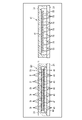
- FIG. 4 is a diagram for explaining an arrangement example of host interfaces in the cassette housing according to the embodiment;
- FIG. 1 is a diagram showing a configuration example of a storage system 1 according to an embodiment.
- the storage system 1 can be used in data centers.
- the X-axis, Y-axis and Z-axis are defined respectively.
- the X-axis, Y-axis and Z-axis are orthogonal to each other.
- An XY plane defined by the X and Y axes corresponds to the floor of the data center.
- the Z axis corresponds to the height direction of the data center.
- the storage system 1 includes a host computer 2, a wafer stocker 3, a cassette 4, a wafer cassette stocker 5, a wafer transfer device 8, and a wafer cassette transfer device 9.
- FIG. 1 illustrates a case where the host computer 2, wafer cassette stocker 5, cassette 4, and wafer stocker 3 (two wafer stockers 3b and 3a) are arranged in a line along the X-axis direction.
- the X-axis runs along the width of each of the host computer 2, wafer cassette stocker 5, cassette 4, and wafer stocker 3.
- the Y-axis runs along the depth of each of the host computer 2, wafer cassette stocker 5, cassette 4, and wafer stocker 3.
- FIG. The Z-axis runs along the height of each of the host computer 2, wafer cassette stocker 5, cassette 4, and wafer stocker 3.
- the storage system 1 uses a semiconductor wafer 40 as a storage medium.
- Semiconductor wafer 40 includes a plurality of non-volatile memory devices.
- the storage system 1 is configured to write data to non-volatile memory devices included in the semiconductor wafer 40 and read data from the non-volatile memory devices included in the semiconductor wafer 40 .
- Each of the multiple nonvolatile memory devices included in the semiconductor wafer 40 is, for example, a NAND flash memory.
- Non-volatile memory devices formed on semiconductor wafers are usually cut out as chips by dicing.
- a diced chip is also referred to as a non-volatile memory die.
- the semiconductor wafer 40 itself including a plurality of nonvolatile memory devices is used as a storage medium.
- a semiconductor wafer 400 used in the storage system 1 has a thickness of 500 ⁇ m or more, for example.
- a semiconductor wafer before the formed nonvolatile memory devices are cut out as chips can be used as the semiconductor wafer 40 .
- a semiconductor wafer obtained by performing a remounting process to collect non-volatile memory dies cut from several semiconductor wafers can be used as the semiconductor wafer 40 .
- a storage system according to a comparative example uses a semiconductor wafer as a storage medium.
- a storage system according to a comparative example includes a prober and a host device.
- a prober includes a probe card and a stage.
- a host device connected to a prober writes data to and reads data from a semiconductor wafer mounted on a stage via a probe card.
- the prober is occupied only by a certain semiconductor wafer while it is being accessed by the host device.
- the semiconductor wafer currently placed on the stage may be removed from the prober and a new semiconductor wafer to be accessed may be placed on the stage. necessary.
- the semiconductor wafer in order to shorten this latency, it is necessary to transfer the semiconductor wafer from the wafer stocker to the prober at high speed. In this case, the semiconductor wafer may be damaged.
- the wafer cassette 90 is used as a storage device accessible by the host device, rather than the host device accessing the semiconductor wafers 40 via the prober.
- Wafer cassette 90 includes cassette housing 80 and semiconductor wafers 40 .
- the host computer 2 includes a host unit 230.
- FIG. 1 illustrates a case where the host computer 2 includes two host units 230a and 230b.
- the number of host units 230 included in the host computer 2 may be one, or three or more.
- the host unit 230 includes slots. At least one wafer cassette 90 can be connected to the slot.
- FIG. 1 illustrates a case where the host unit 230 includes three slots (slots #1 to #3). However, the number of slots included in the host unit 230 may be two or less, or may be four or more.
- the host unit 230 is configured to read data from and write data to the semiconductor wafers 40 (more specifically, each non-volatile memory device included in the semiconductor wafers 40) contained in the wafer cassette 90 connected to the slot. Functions as a host device. Host unit 230 is also configured to communicate with cassette 4, wafer transporter 8, and wafer cassette transporter 9 via an interface. This interface conforms to the Ethernet (registered trademark) standard, for example.
- a server rack is a rack for housing computers and communication equipment.
- the size and shape of server racks are defined, for example, by the Electronic Industries Association of America (EIA).
- a 19-inch rack is 19 inches wide and 1.75 inches high for one unit.
- 19-inch racks having a height of 42 units (19-inch-42U racks) are often used.
- the host computer 2 has a server rack such as a 19 inch rack.
- the host unit 230 has a size that can be accommodated in a server rack.
- the host unit 230 has a height that is, for example, an integral multiple of the height of one unit.
- the host unit 230 may have a size that can be accommodated in the space of one unit of the server rack.
- the host unit 230 may have a size that can be accommodated in a space equivalent to two units of a server rack.
- the host unit 230 may have a size that can be accommodated in the space of three or more units of the server rack.
- the host unit 230 includes a host housing, a system board, and a power supply unit.
- the host housing includes at least one slot to which the wafer cassette 90 can be connected.
- a system board is a printed circuit board on which various electronic components (processor, memory, system controller, communication interface controller, etc.) are mounted.
- the power supply unit is a power supply circuit that supplies power to various electronic components mounted on the system board and the wafer cassette 90 connected to the slot.
- the wafer stocker 3 can store a plurality of semiconductor wafers 40.
- the housing of the wafer stocker 3, like the host computer 2, can also be realized using a server rack such as a 19-inch rack.
- FIG. 1 illustrates a case where the storage system 1 is provided with two wafer stockers 3a and 3b.
- the number of wafer stockers 3 provided in the storage system 1 may be one, or three or more.
- the semiconductor wafer 40 is preferably stored at a low temperature below room temperature (eg, 15 to 25°C). By storing the semiconductor wafer 40 at a low temperature, it is possible to lengthen the retention period of charges stored in each memory cell of the NAND flash memory.
- the wafer stocker 3 may be provided with a temperature control device for cooling the semiconductor wafers 40 .
- the temperature control device may be, for example, a cooling fan.
- the cassette 4 assembles a wafer cassette 90 containing the semiconductor wafers 40 from the semiconductor wafers 40 and the cassette housing 80 .
- the cassette 4 also performs an operation of disassembling the wafer cassette 90 and taking out the semiconductor wafers 40 from the wafer cassette 90 .
- the housing of the cassette 4, like the host computer 2, can also be implemented using a server rack such as a 19-inch rack.
- the wafer cassette stocker 5 can store a plurality of wafer cassettes 90.
- the housing of wafer cassette stocker 5 can also be realized using a server rack such as a 19-inch rack, like host computer 2 .
- Wafer cassette stocker 5 can be used to store not only multiple wafer cassettes 90 but also multiple empty cassette enclosures 80 .
- An empty cassette housing 80 is a cassette housing 80 that does not contain any semiconductor wafers 40 .
- the wafer transfer device 8 is configured to transfer semiconductor wafers 40 between the wafer stocker 3 and the cassette 4 .
- the wafer cassette transfer device 9 is configured to transfer the wafer cassette 90 between the cassette 4, the wafer cassette stocker 5 and the host computer 2.
- the housing of the wafer stocker 3a includes a side plate SP1 and a side plate SP2 located on the opposite side of the side plate SP1 in the X-axis direction.
- An opening a1 may be formed in the side plate SP1.
- An opening b1 may be formed in the side plate SP2.
- Each of the openings a1 and b1 has a size through which the semiconductor wafer 40 can pass.
- the housing of the wafer stocker 3b includes a side plate SP11 and a side plate SP12 located on the opposite side of the side plate SP11 in the X-axis direction.
- the side plate SP12 faces the side plate SP1 of the wafer stocker 3a.
- An opening a2 may be formed in the side plate SP11.
- An opening b2 may be formed in the side plate SP12.
- the opening b2 can be formed at a position facing the opening a1.
- Each of the openings a2 and b2 has a size through which the semiconductor wafer 40 can pass.
- the wafer transfer device 8 can transfer the semiconductor wafer 40 between the wafer stocker 3a and the wafer stocker 3b through the openings a1 and b2.
- the space between the opening a1 and the opening b2 functions as an internal transfer path crossing between the wafer stocker 3a and the wafer stocker 3b.
- a space between the opening a1 and the opening b2 may be covered with a cover member to prevent dust from entering.
- the housing of the cassette 4 includes a side plate SP21 and a side plate SP22 located on the opposite side of the side plate SP21 in the X-axis direction.
- the side plate SP22 faces the side plate SP11 of the wafer stocker 3b.
- An opening a3 may be formed in the side plate SP21.
- An opening b3 may be formed in the side plate SP22.
- the opening b3 can be formed at a position facing the opening a2.
- Each of the openings a3 and b3 has a size through which the semiconductor wafer 40 can pass.
- the wafer transfer device 8 can transfer the semiconductor wafers 40 between the wafer stocker 3b and the cassette 4 through the openings a2 and b3.
- a space between the opening a2 and the opening b3 functions as an internal transfer path traversing between the wafer stocker 3b and the cassette 4.
- a space between the opening a2 and the opening b3 may be covered with a cover member to prevent dust from entering.
- the housing of the wafer cassette stocker 5 includes a side plate SP31 and a side plate SP32 located on the opposite side of the side plate SP31 in the X-axis direction.
- the side plate SP32 faces the side plate SP21 of the cassette 4 .
- An opening a4 may be formed in the side plate SP31.
- An opening b4 may be formed in the side plate SP32.
- the opening b4 can be formed at a position facing the opening a3.
- Each of the opening a4 and the opening b4 has a size through which the wafer cassette 90 can pass.
- the wafer cassette transfer device 9 can transfer the wafer cassette 90 between the cassette 4 and the wafer cassette stocker 5 through the openings a3 and b4.
- a space between the opening a3 and the opening b4 functions as an internal transfer path crossing between the cassette 4 and the wafer cassette stocker 5.
- a space between the opening a3 and the opening b4 may be covered with a cover member to prevent dust from entering.
- the server rack of the host computer 2 includes a side plate SP41 and a side plate SP42 located on the opposite side of the side plate SP41 in the X-axis direction.
- the side plate SP42 faces the side plate SP31 of the wafer cassette stocker 5.
- An opening b5 may be formed in the side plate SP42.
- the opening b5 can be formed at a position facing the opening a4.
- the opening b5 has a size through which the wafer cassette 90 can pass.
- the wafer cassette transfer device 9 can transfer the wafer cassette 90 between the wafer cassette stocker 5 and the host computer 2 through the openings a4 and b5.
- a space between the opening a4 and the opening b5 functions as an internal transfer path crossing between the wafer cassette stocker 5 and the host computer 2.
- FIG. A space between the opening a4 and the opening b5 may be covered with a cover member to prevent dust from entering.
- a semiconductor wafer 40 is transferred through an internal transfer route that traverses between the wafer stocker 3 and the cassette 4, and a wafer cassette 90 is transferred through an internal transfer route that traverses between the cassette 4, the wafer cassette stocker 5, and the host computer 2.
- the transport configuration allows the required semiconductor wafers 40 or the required wafer cassettes 90 to be quickly moved to the required location.
- the time required to assemble the wafer cassette 90 to be accessed including the semiconductor wafers 40 to be accessed and the time required to transport and connect the wafer cassette 90 to be accessed to the slot of the host unit 230 are reduced.
- the semiconductor wafer 40 to be accessed is the semiconductor wafer 40 from which data should be read or written by the host device (host unit 230).
- the wafer cassette 90 to be accessed is the wafer cassette 90 containing the semiconductor wafer 40 to be accessed.
- a transfer device that transfers the semiconductor wafers 40 between the wafer stocker 3 and the cassette 4 without using an internal transfer route crossing between the wafer stocker 3 and the cassette 4 may be used as the wafer transfer device 8.
- the device can also be used as a wafer cassette transport device 9 .
- a transfer robot (see FIG. 6) that moves on the passage in the floor of the data center can be used as such a wafer cassette transfer device 9 as well.
- the host unit 230 has a position management function and a transport control function.
- the position management function manages the positions where each of the plurality of semiconductor wafers 40 exists.
- the transfer control function controls the transfer of the semiconductor wafers 40 and the transfer of the wafer cassette 90 by controlling the cassette 4 , the wafer transfer device 8 and the wafer cassette transfer device 9 .
- a wafer identifier is assigned to each of the plurality of semiconductor wafers 40 .
- Host unit 230 may manage the correspondence between wafer identifiers and the locations where semiconductor wafers 40 identified by the wafer identifiers reside.
- a position where a certain semiconductor wafer 40 can reside is, for example, any one of a plurality of slots in the host unit 230, and a wafer in any one of a plurality of wafer cassette storage positions in the wafer cassette stocker 5.
- the host unit 230 determines the semiconductor wafer 40 to be accessed among the plurality of semiconductor wafers 40 .
- the host unit 230 identifies the location associated with the wafer identifier of the semiconductor wafer 40 to be accessed, thereby determining whether the wafer cassette 90 to be accessed is connected to any slot of the host unit 230 and the access status. It can be determined whether the target wafer cassette 90 is stored in the wafer cassette stocker 5 or not.
- the host unit 230 When the wafer cassette 90 to be accessed is connected to any slot of the host unit 230, the host unit 230 transmits a read request or a write request to the wafer cassette 90 to be accessed. Thereby, the host unit 230 executes data reading or writing with respect to the semiconductor wafer 40 to be accessed.
- the host unit 230 causes the wafer cassette transfer device 9 to transfer the wafer to be accessed.
- the cassette 90 is transported from the wafer cassette stocker 5 to any slot of the host unit 230 and connected.
- the host unit 230 can transmit a transfer request to the wafer cassette transfer device 9 as follows.
- This transfer request designates, for example, a position (wafer cassette storage position) in the wafer cassette stocker 5 where the wafer cassette 90 to be accessed is stored as the transfer source position, and any slot of the host unit 230 is specified. Specify as the destination position.
- the wafer cassette transport device 9 transports the wafer cassette 90 existing at the specified source position to the specified destination position.
- the host unit 230 causes the wafer transfer device 8 to store the semiconductor wafer to be accessed.
- the wafer 40 is transferred from the wafer stocker 3 to the cassette 4.
- the host unit 230 can transmit a transfer request to the wafer transfer device 8 as follows.
- This transfer request designates the position (wafer storage position) in the wafer stocker 3 where the semiconductor wafer 40 to be accessed exists as the transfer source position, and designates the cassette 4 as the transfer destination position.
- the wafer transport device 8 transports the semiconductor wafer 40 existing at the specified source position to the specified destination position.
- the host unit 230 causes the cassette 4 to assemble the wafer cassette 90 to be accessed from the transported semiconductor wafers 40 to be accessed and the cassette housing 80 . Then, the host unit 230 causes the wafer cassette transfer device 9 to transfer the assembled wafer cassette 90 to be accessed from the cassette 4 to one of the slots of the host unit 230 for connection. In this case, the host unit 230 can transmit a transfer request to the wafer cassette transfer device 9 as follows.
- This transport request specifies, for example, the cassette 4 as the source position and specifies one of the slots of the host unit 230 as the destination position.
- the wafer cassette transport device 9 transports the wafer cassette 90 existing at the specified source position to the specified destination position.
- the host unit 230 controls the transportation of the semiconductor wafer 40 to be accessed or the wafer cassette 90 to be accessed, thereby reading or reading data from any semiconductor wafer 40 among the plurality of semiconductor wafers 40 . can be written.
- the host unit 230 may also have a function of managing the priority of each of the plurality of semiconductor wafers 40.
- the algorithm for determining the priority of each of the plurality of semiconductor wafers 40 is not limited to a specific algorithm, and the priority of each of the plurality of semiconductor wafers 40 can be determined based on various conditions.
- the priority of each semiconductor wafer 40 may be determined based on access requests to each semiconductor wafer 40 .
- the priority of each semiconductor wafer 40 may be determined based on the frequency of access to each semiconductor wafer 40 .
- the priority of each semiconductor wafer 40 may be determined based on the elapsed time from the last access time to each semiconductor wafer 40 .
- the priority of each semiconductor wafer 40 may be determined based on the status indicating completion or incompleteness of access processing for each semiconductor wafer 40 .
- the priority of each semiconductor wafer 40 may be determined based on the expected remaining time until the access process for each semiconductor wafer 40 is completed.
- the priority of each semiconductor wafer 40 may be determined based on the application program being executed.
- the priority of each semiconductor wafer 40 may be determined based on the prediction result of the probability that an access request to each semiconductor wafer 40 will occur.
- Each semiconductor wafer 40 may be prioritized using a combination of two or more conditions.
- the host unit 230 can also control the position where each of the plurality of semiconductor wafers 40 exists based on the priority of each of the plurality of semiconductor wafers 40 .
- the host unit 230 may have a wafer cassette 90 containing semiconductor wafers 40 having a first level of priority connected to a slot of the host unit 230 and a wafer cassette 90 containing semiconductor wafers 40 having a second level of priority being connected to a slot of the host unit 230 .
- the position of each of the plurality of semiconductor wafers 40 may be controlled such that the semiconductor wafers 40 stored in the wafer cassette stocker 5 and having a third level of priority are stored in the wafer stocker 3 .
- the second level priority is lower than the first level priority.
- the third level priority is lower than the second level priority.
- the highest priority and the second highest priority are the first level. equivalent to the priority of Also, the third highest priority and the fourth highest priority correspond to the second level priority.
- the fifth and lower set of priorities correspond to the third level of priority.
- the host unit 230 places the two wafer cassettes 90 corresponding to the two semiconductor wafers 40 with the first level priority into the two slots of the host unit 230 regardless of access requests to the individual semiconductor wafers 40 . may be connected to each.
- the host unit 230 stores two wafer cassettes 90 corresponding to the two semiconductor wafers 40 having the second level of priority in the wafer cassette stocker 5 regardless of access requests to individual semiconductor wafers 40 . good too.
- the host unit 230 may store a plurality of semiconductor wafers 40 having a third level of priority in the wafer stocker 3 regardless of access requests for individual semiconductor wafers 40 .
- the host unit 230 determines this semiconductor wafer 40 as the semiconductor wafer 40 to be assembled.
- the semiconductor wafers 40 to be assembled are the semiconductor wafers 40 to be assembled into the wafer cassette 90 .
- the host unit 230 causes the wafer transfer device 8 to transfer the semiconductor wafer 40 to be assembled from the wafer stocker 3 to the cassette 4 .
- the host unit 230 can transmit a transfer request to the wafer transfer device 8 as follows.
- This transfer request designates the position (wafer storage position) in the wafer stocker 3 where the semiconductor wafer 40 to be assembled exists as the transfer source position, and designates the cassette 4 as the transfer destination position.
- the wafer transport device 8 transports the semiconductor wafer 40 existing at the specified source position to the specified destination position.
- the host unit 230 causes the cassette 4 to assemble the wafer cassette 90 from the transported semiconductor wafers 40 to be assembled and the cassette housing 80 .
- the host unit 230 causes the wafer cassette transfer device 9 to transfer the assembled wafer cassette 90 from the cassette 4 to the wafer cassette stocker 5 .
- the host unit 230 can transmit a transfer request to the wafer cassette transfer device 9 as follows.
- This transfer request specifies, for example, the cassette 4 as the transfer source position and the position in the wafer cassette stocker 5 (wafer cassette storage position) as the transfer destination position.
- the wafer cassette transport device 9 transports the wafer cassette 90 existing at the specified source position to the specified destination position.
- this semiconductor wafer 40 is actually determined as the semiconductor wafer 40 to be accessed, since the wafer cassette 90 containing this semiconductor wafer 40 is already stored in the wafer cassette stocker 5, data reading or It is possible to reduce the required latency until writing becomes possible.
- FIG. 2 is a diagram showing a configuration example of the semiconductor wafer 40. As shown in FIG. A semiconductor wafer 40 is used as a storage medium in the storage system 1 .
- a semiconductor wafer 40 includes a plurality of nonvolatile memory devices 70 .
- the size of the semiconductor wafer 40 is not limited, but may be a 300 mm wafer.
- the number of nonvolatile memory devices 70 included in one semiconductor wafer 40 is 1024 and the storage capacity of one nonvolatile memory device 70 is 32 Gbytes, the storage capacity of one semiconductor wafer 40 is 32 Tbytes.
- the nonvolatile memory device 70 has, for example, a rectangular shape, and a plurality of electrodes (pads) 41 electrically connectable to the outside are arranged on one side thereof.
- the identification information storage area 71 is used as a storage area for storing identification information and check codes.
- Identification information is issued by the host unit 230 to identify this semiconductor wafer 40 .
- an identifier wafer identifier
- a check code is a code for verifying the integrity of identification information. Examples of check codes include a cyclic redundancy code (CRC), another type of parity different from the CRC, and a hash value calculated from identification information.
- CRC cyclic redundancy code
- identification information storage area 71 By storing a pair of identification information and a check code in the identification information storage area 71, it is possible to verify the consistency of the value read as the identification information from the identification information storage area 71. Therefore, a random value stored in the identification information storage area 71 of a new semiconductor wafer 40 immediately after shipment from the factory (that is, a semiconductor wafer 40 in which pairs of identification information and inspection code are not stored) is mistakenly used as identification information. It is possible to prevent being handled.
- the management data includes, for example, wafer control information necessary for writing data to and reading data from the semiconductor wafer 40 .
- wafer control information includes a logical/physical address conversion table corresponding to the semiconductor wafer 40 .
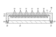
- FIG. 3 is a diagram showing a configuration example of the wafer cassette 90.
- Wafer cassette 90 is used as a storage device in storage system 1 .
- Wafer cassette 90 includes semiconductor wafers 40 and cassette housing 80 .
- the cassette housing 80 includes a lower case 21 and an upper case 31.
- a semiconductor wafer 40 can be placed on the lower case 21 .
- Lower case 21 includes a wafer mounting area for mounting semiconductor wafer 40 thereon.
- Lower case 21 and upper case 31 can be joined together.
- the upper case 31 contains the probe card 11 .
- the probe card 11 may be independent from the upper case 31 . That is, the probe card 11 is not an essential component of the cassette housing 80.
- the probe card 11 includes a substrate having a bottom surface and a top surface opposite to the bottom surface.
- the lower surface faces the semiconductor wafer 40 mounted on the wafer mounting area within the lower case 21 .
- a plurality of probe pins 51 are arranged on the bottom surface of the probe card 11 .
- the plurality of probe pins 51 can contact the plurality of pads 41 of the semiconductor wafer 40 placed in the wafer placement area inside the lower case 21 .
- Each probe pin 51 is used to supply electrical signals to or receive electrical signals from pads 41 of semiconductor wafer 40 .
- the probe pin 51 is also called a probe or probe needle.
- the total number of probe pins 51 arranged on the bottom surface of probe card 11 may be the same as the total number of pads 41 in semiconductor wafer 40 . In this case, the probe card 11 can be collectively connected to a plurality of pads 41 within the semiconductor wafer 40 . This can increase the number of non-volatile memory devices 70 that can be accessed in parallel.
- a controller 61 is arranged on the top surface of the probe card 11 .
- Controller 61 is a memory controller configured to control a plurality of non-volatile memory devices 70 within semiconductor wafer 40 .
- the controller 61 may be implemented by a large scale integration (LSI) such as a system-on-a-chip (SoC).
- LSI large scale integration
- SoC system-on-a-chip
- FIG. 3 illustrates a configuration example in which a plurality of controllers 61 are arranged on the top surface of the probe card 11 .
- the number of controllers 61 arranged on the top surface of the probe card 11 may be one, or two or more.
- the controller 61 may function as a Flash Translation Layer (FTL) configured to perform data management for each non-volatile memory device 70 within the semiconductor wafer 40 .
- Data management performed by the FTL includes management of mapping information indicating the correspondence between each logical address and each physical address of the plurality of non-volatile memory devices 70, and the like.
- a logical address is an address used by host unit 230 to address a location within the logical address space of semiconductor wafer 40 to be accessed.
- a physical address corresponding to a logical address points to the physical storage location within non-volatile memory device 70 where the data corresponding to the logical address is written.
- LBA logical block address (addressing)
- the cassette housing 80 includes a non-volatile memory.
- An identifier for identifying the cassette housing 80 can be stored in this nonvolatile memory.
- This non-volatile memory may be implemented within the controller 61 .
- FIG. 4 is a diagram showing a configuration example of the cassette 4. As shown in FIG. Cassette 4 performs assembly and disassembly of wafer cassette 90 .
- the cassette 4 assembles the wafer cassette 90 by mechanically joining the lower case 21 on which the semiconductor wafers 40 are placed and the upper case 31 .
- the cassette 4 aligns the pads 41 of the semiconductor wafer 40 with the probe pins 51 of the probe card 11 .
- the cassette 4 joins the lower case 21 and the upper case 31 together so that the plurality of probe pins 51 are in contact with the plurality of pads 41 .
- the cassette 4 includes a stage 401 and an actuator 402.
- the stage 401 has a mechanism that holds the lower case 21 .
- the cassette 4 places the semiconductor wafers 40 transferred from the wafer stocker 3 to the cassette 4 by the wafer transfer device 8 on the lower case 21 placed on the stage 401 .
- the actuator 402 moves the upper case 31 or the stage 401 in the Z-axis direction to bring the pads 41 of the semiconductor wafer 40 into contact with the probe pins 51 of the probe card 11 .
- the lower case 21 and the upper case 31 are joined together.
- the semiconductor wafer 40 is accommodated in the cassette housing 80 .
- the plurality of pads 41 of the semiconductor wafer 40 and the plurality of probe pins 51 of the probe card 11 are brought into contact with each other, thereby electrically connecting the controller 61 and the semiconductor wafer 40 (more specifically, the plurality of nonvolatile memory devices 70). Connected.
- the actuator 402 moves the upper case 31 or the stage 401 in the Z-axis direction to the opposite side from the time of assembly, thereby separating the upper case 31 and the lower case 21 from each other.
- FIG. 5 is a diagram showing a configuration example of the host computer 2 included in the storage system 1. As shown in FIG. 5
- FIG. 5 illustrates a case where two host units 230a and 230b are accommodated in the server rack for the host computer 2.
- FIG. Each of the host units 230a, 230b functions as a host device.
- Each of the host units 230a, 230b includes one or more slots, eg, three slots (slots #1-#3).
- a wafer cassette 90 can be detachably inserted into each of the slots #1 to #3.
- FIG. 6 is a plan view showing an arrangement example of wafer stockers 3a to 3c, cassette 4, wafer cassette stocker 5, host computer 2, wafer transfer device 8, and wafer cassette transfer device 9 included in storage system 1.
- FIG. 6 is a plan view showing an arrangement example of wafer stockers 3a to 3c, cassette 4, wafer cassette stocker 5, host computer 2, wafer transfer device 8, and wafer cassette transfer device 9 included in storage system 1.
- server racks On the floor (XY plane) in the data center, a plurality of server racks are arranged so that the front side of the server rack (for example, the front door of the server rack) faces the aisle.
- server racks accommodating various computers other than the storage system 1 are represented as general server racks.
- the wafer stocker 3c has the same configuration as the wafer stockers 3a and 3b described with reference to FIG.
- Each of the wafer stockers 3a to 3c, the cassette 4, the wafer cassette stocker 5, and the host computer 2 can also be arranged so that the front side of the server rack (for example, the front door of the server rack) faces the aisle.
- the transport robot 101 is a mobile transport robot that can move on passages.
- the transfer robot 101 can function as a wafer transfer device that transfers the semiconductor wafers 40 between the wafer stockers 3a to 3c and the cassette 4.
- the transfer robot 101 has an arm capable of taking the semiconductor wafer 40 in and out of each server rack.
- the transfer robot 101 adds the semiconductor wafers 40 to the wafer stockers 3a to 3c and the cassette 4 through the front side thereof. Further, the transfer robot 101 takes out the semiconductor wafer 40 from each of the wafer stockers 3a to 3c and the cassette 4 through the front side thereof.
- the transfer robot 101 transfers the semiconductor wafer 40 through an internal transfer path (that is, a pair of openings b3 and a2, a pair of openings b2 and a1, and a pair of openings b1 and a0) that traverses between the wafer stockers 3a to 3c and the cassette 4.
- an internal transfer path that is, a pair of openings b3 and a2, a pair of openings b2 and a1, and a pair of openings b1 and a0
- an internal transfer path that is, a pair of openings b3 and a2, a pair of openings b2 and a1, and a pair of openings b1 and a0
- Each of the transport robots 102 and 103 is a mobile transport robot that can move on a passage.
- Each of the transfer robots 102 and 103 can function as a wafer cassette transfer device that transfers the wafer cassette 90 between the host computer 2 , wafer cassette stocker 5 and cassette 4 .
- Each of the transport robots 102 and 103 has an arm capable of loading and unloading the wafer cassette 90 with respect to each server rack.
- Each of the transfer robots 102 and 103 adds the wafer cassette 90 to each of the host computer 2, wafer cassette stocker 5 and cassette 4 through the front side thereof. Further, each of the transfer robots 102 and 103 takes out the wafer cassette 90 from each of the host computer 2, the wafer cassette stocker 5 and the cassette 4 through the front side thereof.
- Each of the transfer robots 102 and 103 transfers the semiconductor wafer 40 through an internal transfer path (that is, the pair of openings b5 and a4, the pair of openings b4 and a3) that traverses between the host computer 2, the wafer cassette stocker 5 and the cassette 4. can be used instead of or in addition to the wafer cassette transporter 9 that transports the .
- FIG. 7 is a plan view showing a configuration example of the wafer stocker 3.
- FIG. 7 is a plan view showing a configuration example of the wafer stocker 3.
- the housing of the wafer stocker 3 is realized using, for example, a deep 19-inch rack with a depth of 36 inches (914.4 mm).
- a robot arm 80 is arranged at a central position between the front surface of the wafer stocker 3 and the back surface of the wafer stocker 3 in order to efficiently utilize the depth of 36 inches.
- Both sides of the robot arm 80 that is, both the space between the robot arm 80 and the front surface of the wafer stocker 3 and the space between the robot arm 80 and the back surface of the wafer stocker 3, hold a plurality of semiconductor wafers, each of which is a 300 mm wafer. Used as a storage location for wafers 40 .
- a robot arm 80a and a robot arm 80b arranged in each of the wafer stockers 3a and 3b function as a wafer transfer device 8.
- the semiconductor wafer 40 is transferred between the robot arms 80a and 80b through the openings a1 and b2.
- FIG. 8 is a diagram showing a configuration example of a robot arm 80 used as the wafer transfer device 8. As shown in FIG.
- FIG. 8 illustrates a configuration including a base 81, a support 82, an arm 83, and a grip portion 84.
- the strut 82 has one end supported by the base 81 .
- the strut 82 is extendable in the Z-axis direction.
- Arm 83 is attached to the other end of support 82 .
- Arm 83 is configured to rotate about post 82 .
- a grip portion 84 is attached to the tip of the arm 83 .
- the grasping part 84 is, for example, a suction head or a robot hand.
- the wafer cassette transfer device 9 can also be realized by robot arms arranged in the host computer 2, the wafer cassette stocker 5, and the cassette 4, similarly to the wafer transfer device 8.
- FIG. 9A is a view showing part of the operation of transferring the semiconductor wafer 40 from the wafer stocker 3b to the wafer stocker 3a through the opening b2 of the side plate SP12 of the wafer stocker 3b and the opening a1 of the side plate SP1 of the wafer stocker 3a.
- the positions of the arm 83 of the robot arm 80b placed on the wafer stocker 3b and the arm 83 of the robot arm 80a placed on the wafer stocker 3a are initial positions.
- the support column 82 of the robot arm 80b contracts, causing the arm 83 to move.
- the semiconductor wafer 40 to be transferred is lowered to the storage position.
- the post 82 of the robot arm 80b rotates to move the arm 83 above the semiconductor wafer 40 to be transferred.
- the arm 83 of the robot arm 80b grips the semiconductor wafer 40 to be transferred by the gripper 84 .
- Post 82 raises arm 83 to the position of the internal transport path including opening b2 and opening a1.
- the arm 83 conveys the semiconductor wafer 40 to be conveyed to the internal conveying path.
- the arm 83 of the robot arm 80a is moved above the semiconductor wafer 40 to be transferred, and the gripper 84 grips the semiconductor wafer 40 to be transferred.
- FIG. 9B shows the rest of the operation of transferring the semiconductor wafer 40 from wafer stocker 3b to wafer stocker 3a.
- the arm 83 of the robot arm 80b releases the semiconductor wafer 40 to be transferred and returns to the initial position.
- the arm 83 of the robot arm 80a transports the semiconductor wafer 40 to be transported to the destination storage position.
- the arm 83 of the robot arm 80a releases the semiconductor wafer 40 to be transferred and returns to the initial position.
- FIG. 10 is a plan view showing an arrangement example of a plurality of robot arms used as the wafer transfer device 8 and the wafer cassette transfer device 9 of FIG. 6, respectively.
- robot arms 8a to 8c are arranged at central positions within wafer stockers 3a to 3c, respectively.
- robot arms 9a and 9b are arranged at the central positions of cassette 4 and wafer cassette stocker 5, respectively.
- the robot arms 8a to 8c and the robot arm 9a function as a wafer transfer device 8. Further, the robot arms 9a and 9b function as a wafer cassette transfer device 9 that transfers the wafer cassette 90 between the cassette 4 and the wafer cassette stocker 5 through the openings a3 and b4.
- Transfer of the wafer cassette 90 between the wafer cassette stocker 5 and the host computer 2 can also be performed by the transfer robot 102 or 103.
- the transfer robot 102 or 103 takes out the wafer cassette 90 from the wafer cassette stocker 5 through the front surface of the wafer cassette stocker 5 and moves to the front surface of the host computer 2 . Then, the transfer robot 102 or 103 connects the wafer cassette 90 to the slot of the host unit 230 through the front surface of the host computer 2 .
- transfer robot 102 or 103 takes wafer cassette 90 out of the slot of host unit 230 through the front of host computer 2 and moves it to the front of wafer cassette stocker 5 or cassette 4 . Then, the transfer robot 102 or 103 puts the wafer cassette 90 taken out from the slot of the host unit 230 into the wafer cassette stocker 5 or cassette 4 through the front surface of the wafer cassette stocker 5 or cassette 4 .
- FIG. 11 is a plan view showing another arrangement example of a plurality of robot arms used as the wafer transfer device 8 and the wafer cassette transfer device 9 in FIG.
- robot arms 8a to 8c are arranged at central positions within wafer stockers 3a to 3c, respectively.
- robot arms 9a to 9c are arranged at the central positions of cassette 4, wafer cassette stocker 5 and host computer 2, respectively.
- the robot arms 8a to 8c and the robot arm 9a function as the wafer transfer device 8 in FIG. Further, the robot arms 9a to 9c function as the wafer cassette transfer device 9 in FIG.
- the wafer cassette 90 is assembled in the cassette 4.
- the wafer cassette 90 is transferred from the robot arm 9a to the robot arm 9b.
- the wafer cassette 90 is transferred from the robot arm 9b to the robot arm 9c.
- Robot arm 9 c connects wafer cassette 90 to a slot of host unit 230 .
- the robot arm 9c removes the wafer cassette 90 from the slot of the host unit 230 and transfers the removed wafer cassette 90 to the robot arm 9b.
- the robot arm 9b carries this wafer cassette 90 to a storage position in the wafer cassette stocker 5 or transfers it to the robot arm 9a.
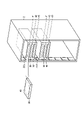
- FIG. 12 is a diagram showing a configuration example of the wafer cassette 90. As shown in FIG. 12
- Wafer cassette 90 includes a plurality of plug terminals 22 provided on the back of thin box-shaped cassette housing 80 .
- Each of the multiple plug terminals 22 is a host interface for communicating with the host unit 230 .
- Each plug terminal 22 is, for example, a PCIe male terminal conforming to the PCI express TM (PCIe TM ) standard or a male terminal for Ethernet.
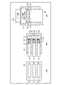
- FIG. 13 is a diagram showing a configuration example of the host unit 230. As shown in FIG. 13
- FIG. 13 The left part of FIG. 13 is a diagram of the host unit 230 viewed from the front side.
- the central portion of FIG. 13 is a side view of the host unit 230 .
- the right part of FIG. 13 is a view of the host unit 230 viewed from the top side.
- the host unit 230 includes three slots #1-#3. Each of slots #1-#3 has a cavity capable of accommodating wafer cassette 90 therein. The left part of FIG. 13 shows a case where wafer cassettes 90 are accommodated in each of these slots #1 to #3.
- a plurality of receptor terminals 232 are provided for each slot.
- Each of the plurality of receptor terminals 232 is, for example, a PCIe female terminal or a female terminal for Ethernet.
- the above-described system board, also called a host board, and a power supply unit are provided as components 231 .
- a system board (host board) is provided with a processor, a memory, a system controller, a communication interface controller, and the like.
- the plurality of plug terminals 22 of the wafer cassette 90 are connected to the plurality of receptor terminals 232 provided on the inner side of this slot.
- Each of these receptor terminals 232 is electrically connected to the system board.
- FIG. 14 is a block diagram showing a configuration example of the host unit 230. As shown in FIG. 14
- the host unit 230 includes a processor 201, main memory 202, system controller 203, communication interface controller 204, and the like.
- the processor 201 , main memory 202 , system controller 203 and communication interface controller 204 are mounted on the system board of the host unit 230 .
- the main memory 202 is, for example, dynamic random access memory (DRAM).
- DRAM dynamic random access memory
- the communication interface controller 204 communicates with the cassette 4, the wafer transfer device 8, and the wafer cassette transfer device 9 via the communication interface 205.
- the communication interface 205 for example, an interface conforming to the Ethernet standard can be used.
- communication interface controller 204 may be implemented by, for example, a network interface controller (NIC).
- NIC network interface controller
- the processor 201 executes various programs (software) loaded into the main memory 202 . These programs may include, for example, an application program 211, an operating system (OS) 212, a file system 213, a device driver 214 for controlling the wafer cassette 90, a storage management tool 216, and the like.
- the storage management tool 216 is a program for managing each semiconductor wafer 40 , each cassette housing 80 , and each wafer cassette 90 , and for controlling transportation of each semiconductor wafer 40 and each wafer cassette 90 .
- the statement that these programs execute a certain process means that the process is executed by the host unit 230 (more specifically, the processor 210) executing these programs.
- the host unit 230 (more specifically, the processor 210) can manage the wafer management table 221 under the control of the storage management tool 216.
- the wafer management table 221 is management data for multiple semiconductor wafers 40 in the wafer stocker 3 .
- the host unit 230 can manage the cassette management table 222 under the control of the storage management tool 216.
- the cassette management table 222 is management data for multiple cassette housings 80 or multiple wafer cassettes 90 in the wafer cassette stocker 5 .
- the wafer management table 221 and the cassette management table 222 may be stored in the main memory 202. At least part of the information managed by the wafer management table 221 corresponding to a certain semiconductor wafer 40 may be stored in the storage area of this semiconductor wafer 40 .
- the host unit 230 is configured to give each semiconductor wafer 40 a unique identifier.
- the host unit 230 uses the wafer management table 221 to manage the identifier of each semiconductor wafer 40 , the priority of each semiconductor wafer 40 , the state of each semiconductor wafer 40 , and the positional information of each semiconductor wafer 40 .
- 14 shows an example in which the host unit 230 identifies each of the plurality of semiconductor wafers 40 used in the storage system 1 using wafer identifiers W#1, W#2, . . . , W#n. It is
- the host unit 230 stores the priority of each of the plurality of semiconductor wafers 40 in the wafer management table 221. Based on the priority managed by the wafer management table 221, the host unit 230 transfers the semiconductor wafers 40, the cassette housings 80, and the wafer cassettes 90 to the wafer transfer device 8 and the wafer cassette transfer device 9. Instructs the transport process.
- the host unit 230 stores, as the state of each semiconductor wafer 40, information indicating in which of the host computer 2, wafer cassette stocker 5, and wafer stocker 3 each of the plurality of semiconductor wafers 40 is located in the wafer management table 221. .
- the host unit 230 can recognize that the wafer cassette 90 containing this semiconductor wafer 40 is connected to the slot of the host unit 230.
- the host unit 230 can recognize that the wafer cassette 90 containing this semiconductor wafer 40 is stored in the wafer cassette stocker 5. That is, the host unit 230 can recognize that this semiconductor wafer 40 has already been assembled as a wafer cassette 90 .
- the host unit 230 can recognize that this semiconductor wafer 40 is stored in the wafer stocker 3 . That is, the host unit 230 can recognize that this semiconductor wafer 40 has not yet been assembled in the wafer cassette 90 .
- the host unit 230 stores the position information of the semiconductor wafers 40 in the wafer management table 221 as information indicating the positions where each of the plurality of semiconductor wafers 40 is connected or stored.
- the host unit 230 stores the slot number indicating the slot of the host unit 230 to which the wafer cassette 90 containing this semiconductor wafer 40 is connected as the positional information of this semiconductor wafer 40 . are stored in the wafer management table 221 as.
- the host unit 230 stores the storage position number indicating the position in the wafer cassette stocker 5 where the wafer cassette 90 containing this semiconductor wafer 40 is stored.
- the position information of the semiconductor wafer 40 is stored in the wafer management table 221 .
- the host unit 230 uses the storage position number indicating the position in the wafer stocker 3 where this semiconductor wafer 40 is stored as the position information of this semiconductor wafer 40. Stored in wafer management table 221 .
- the host unit 230 is configured to give a unique identifier to each cassette housing 80 .
- the host unit 230 uses the cassette management table 222 to manage the identifier of each cassette housing 80, the state of each cassette housing 80, and the positional information of each cassette housing 80.
- FIG. 14 shows an example in which the host unit 230 identifies each of the plurality of cassette housings 80 used in the storage system 1 using cassette identifiers C#1, C#2, . . . , C#m. It is shown.
- the host unit 230 stores in the cassette management table 222 information indicating whether each of the plurality of cassette housings 80 is empty, assembled in the wafer cassette 90, or disabled.
- the host unit 230 When a certain cassette housing 80 is stored in the wafer cassette stocker 5 without containing any semiconductor wafers 40, the host unit 230 provides information indicating that this cassette housing 80 is an empty cassette housing. Information indicating the state of the cassette housing 80 is stored in the cassette management table 222 .
- the host unit 230 has assembled a wafer cassette 90 with a certain semiconductor wafer 40 together with a certain cassette housing 80
- the wafer identifier of the semiconductor wafer 40 contained in this cassette housing 80 (wafer cassette 90) is transferred to this It is stored in the cassette management table 222 as information indicating the state of the cassette housing 80 .
- the host unit 230 stores information indicating that this cassette housing 80 is in a prohibited state as information indicating the state of this cassette housing 80. Stored in the cassette management table 222 .
- the host unit 230 stores in the cassette management table 222 position information indicating the positions where each of the plurality of cassette housings 80 is connected or stored.
- FIG. 14 shows an example in which the host unit 230 stores information indicating one of the components of the storage system 1 in the cassette management table 222 as position information.
- the host unit 230 assigns the slot number indicating the slot of the host unit 230 to which the wafer cassette 90 including this cassette housing 80 is connected to this cassette housing 80. may be stored in the cassette management table 222 as the positional information.
- the host unit 230 assigns a storage position number indicating the storage position within the wafer cassette stocker 5 where this wafer cassette 90 is stored. , may be stored in the cassette management table 222 as the position information of the cassette housing 80 .
- the host unit 230 stores the storage position number indicating the storage position within the wafer cassette stocker 5 where this empty cassette housing 80 is stored. It may be stored in the cassette management table 222 as position information of the cassette housing 80 .
- the semiconductor wafer 40 having the wafer identifier W#1 is connected to the slot #1 of the host unit 230.
- the semiconductor wafer 40 having the wafer identifier W#2 is in the state of the wafer cassette 90 stored in the cassette housing 80 and stored at the storage position #2 in the wafer cassette stocker 5.
- a semiconductor wafer 40 having a wafer identifier W#n is stored in a wafer stocker 3 at a storage position #3.
- the cassette housing 80 having the cassette identifier C#1 is already assembled as a wafer cassette 90 containing the semiconductor wafers 40 having the wafer identifier W#1, and is connected to the slot #1 of the host unit 230. .
- the cassette housing 80 having the cassette identifier C#2 is set to be prohibited from being used, and is stored at the storage position #1 in the wafer cassette stocker 5.
- FIG. The cassette housing 80 having the cassette identifier C#m is in the state of an empty cassette housing 80 that does not contain any semiconductor wafers 40 and is stored at the storage position #3 within the wafer cassette stocker 5 .
- wafers A to E are hereinafter referred to as wafers A to E, respectively.
- FIG. 15A is a diagram for explaining swap operations performed in the storage system 1 according to the embodiment.
- the swap operation replaces the wafer cassette 90 connected to the slot of the host unit 230 with another wafer cassette 90 in the wafer cassette stocker 5 .
- the number of slots provided in the host unit 230 is two.
- the host unit 230 controls the wafer cassette transfer device 9 to Perform swap operations.
- the host unit 230 determines the semiconductor wafer 40 to be accessed from among the plurality of semiconductor wafers 40 included in the storage system 1 .
- the wafer C is determined as the semiconductor wafer 40 to be accessed.
- the host unit 230 for example, access request, access frequency, elapsed time from the last access time, completion or non-completion of access processing, expected remaining time until completion of access processing, application program to be executed, result of access probability prediction, etc., the priority of each semiconductor wafer 40 can be dynamically changed. For example, if an access request for wafer C arises, the priority of wafer C can be increased.
- each semiconductor wafer 40 connected as a wafer cassette 90 to the slot of the host unit 230 is determined according to the completion of the access processing for each semiconductor wafer 40 or the final access time for each semiconductor wafer 40. can be lowered depending on how much time has passed since.
- the priority of each semiconductor wafer 40 managed by the storage system 1 is changed by the host unit 230.
- the priority of wafer C is changed from 3rd to 1st
- the priority of wafer A is changed from 1st to 2nd
- the priority of wafer B is changed from 2nd to 3rd. is assumed.
- the host unit 230 uses one of the wafer cassettes 90 connected to the slots of the host unit 230 (here, the wafer cassette 90 containing the wafer A and the wafer cassette 90 containing the wafer B). , the wafer cassette 90 containing the semiconductor wafer 40 having the lowest priority is determined as the wafer cassette 90 to be replaced.
- the wafer cassette 90 containing the wafer B is determined as the wafer cassette 90 to be replaced.
- the host unit 230 transports the wafer cassette 90 (wafer cassette (wafer B)) containing the wafer B from the slot #2 of the host unit 230 to the wafer cassette stocker 5, and wafer cassette 90 (wafer cassette (wafer C)) containing .
- the wafer cassette (wafer B) is removed from the slot #2 of the host unit 230 and stored in the storage position #11 inside the wafer cassette stocker 5, for example.
- a wafer cassette (wafer C) is connected to slot # 2 of host unit 230 .
- the host unit 230 updates the wafer management table 221 so that the priority, status, and position information of each semiconductor wafer 40 show the latest contents.
- the wafer cassette (wafer B) connected to the slot #2 of the host unit 230 and the wafer cassette (wafer C) stored in the wafer cassette stocker 5 are transferred by the process described with reference to FIG. 15A.
- a swap operation is performed to replace the
- FIG. 10 is a diagram for explaining operations performed in the storage system 1 according to the embodiment when
- the priority of each semiconductor wafer 40 is changed by the host unit 230.
- the priority of the wafer E existing in the wafer stocker 3 is changed from 5th to 3rd.
- the priority of wafer C is changed from 3rd to 4th and the priority of wafer D in wafer cassette stocker 5 is changed from 4th to 5th.
- the host unit 230 selects the wafer cassette 90 containing the semiconductor wafer 40 with the lowest priority from among the wafer cassettes 90 stored in the wafer cassette stocker 5 .
- the wafer cassette 90 containing the wafer D (wafer cassette (wafer D)) is selected.
- the host unit 230 instructs the wafer cassette transfer device 9 to transfer the wafer cassette (wafer D) from the wafer cassette stocker 5 to the cassette 4 .
- the host unit 230 instructs the wafer transfer device 8 to transfer the wafer E whose priority has been raised from the fifth to the third from the wafer stocker 3 to the cassette 4 . Thereby, the wafer cassette (wafer D) and the wafer E are transferred to the cassette 4 .
- the host unit 230 instructs the cassette 4 to disassemble the wafer cassette (wafer D) into the wafer D and the empty cassette housing 80 .
- the cassette 4 disassembles the transferred wafer cassette (wafer D) into the wafer D and an empty cassette housing 80 .
- the host unit 230 instructs the cassette 4 to assemble the wafer cassette 90 containing the wafer E from the empty cassette housing 80 and the wafer E (wafer cassette (wafer E)).
- the cassette 4 assembles a wafer cassette (wafer E) from the empty cassette housing 80 and the wafer E.
- the empty cassette housing 80 used to assemble the wafer cassette (wafer E) may be the empty cassette housing 80 obtained by disassembling the wafer cassette (wafer D).
- the host unit 230 instructs the wafer cassette transfer device 9 to transfer the assembled wafer cassette (wafer E) from the cassette 4 to the storage position #12 in the wafer cassette stocker 5. Then, the host unit 230 transports the wafer D taken out from the wafer cassette (wafer D) by disassembling the wafer cassette (wafer D) from the cassette 4 to the storage position #111 in the wafer stocker 3. Point to 8.
- the wafer cassette (wafer E) is stored at the storage position #12 within the wafer cassette stocker 5, and the wafer D is stored at the storage position #111 within the wafer stocker 3.
- the host unit 230 updates the wafer management table 221 so that the priority, status, and position information of each semiconductor wafer 40 show the latest contents.
- wafer E stored at storage position #111 in wafer stocker 3 is transferred to cassette 4 in response to updating the priority of each semiconductor wafer 40.
- a wafer cassette 90 containing wafers E is assembled.
- 16A-16F illustrate the case where the host unit 230 of the host computer 2 has four slots and the wafer cassette stocker 5 has four storage positions.
- FIG. 16A is a diagram for explaining the operation performed in the storage system 1 according to the embodiment when the wafer cassette 90 to be accessed has already been connected to the slot of the host unit 230.
- FIG. 16A is a diagram for explaining the operation performed in the storage system 1 according to the embodiment when the wafer cassette 90 to be accessed has already been connected to the slot of the host unit 230.
- four wafer cassettes 90 each containing four wafers A to D having priorities of 1st to 4th are connected to slot #1 to slot #4 of the host unit 230, respectively.
- Four wafer cassettes 90 each containing four wafers E to H having the fifth to eighth priority are stored in storage positions #11 to #14 in the wafer cassette stocker 5, respectively.
- Two wafers I to J having the 9th to 10th priorities are stored in storage positions #111 to #112 in the wafer stocker 3, respectively.
- the host unit 230 determines the wafer D as the semiconductor wafer 40 to be accessed. As described above, if an access request for wafer D arises, the priority of wafer D may be increased. In addition, the priority of each of the semiconductor wafers 40 (here, wafers A to C) contained in the other wafer cassettes 90 connected to the slots of the host unit 230 is, for example, the completion of the access process for that semiconductor wafer 40. or according to the elapsed time since the last access time for the semiconductor wafer 40 . In FIG.
- the priority of wafer D is changed from 4th to 1st
- the priority of wafer A is changed from 1st to 2nd
- the priority of wafer B is changed from 2nd to 3rd
- the priority of wafer B is changed from 2nd to 3rd. It is assumed that the priority of C is changed from 3rd to 4th.
- the host unit 230 refers to the wafer management table 221 and recognizes that the wafer cassette 90 (wafer cassette (wafer D)) containing the wafer D to be accessed is already connected to slot #4 of the host unit 230.
- the host unit 230 transmits a read command or write command to the wafer cassette (wafer D) connected to slot #4, thereby reading data from or writing data to wafer D.
- FIG. 16B is for explaining the operation performed in the storage system 1 according to the embodiment when there is an empty slot in the host unit 230 and the wafer cassette 90 to be accessed is stored in the wafer cassette stocker 5. is a diagram.
- Three wafer cassettes 90 each containing three wafers A to C having priorities of 1st to 3rd are connected to slot #1 to slot #3 of the host unit 230, respectively.
- Slot #4 is an empty slot to which no wafer cassette 90 is connected.
- four wafer cassettes 90 each containing four wafers D to G having the fourth to seventh priorities are stored in storage positions #11 to #14 in the wafer cassette stocker 5, respectively.
- three wafers H to J having priorities of eighth to tenth are stored in storage positions #111 to #113 in the wafer stocker 3, respectively.
- the host unit 230 determines the wafer D as the semiconductor wafer 40 to be accessed.
- the priority of each semiconductor wafer 40 can be changed by the host unit 230 .
- the priority of wafer D is changed from 4th to 1st
- the priority of wafer A is changed from 1st to 2nd
- the priority of wafer B is changed from 2nd to 3rd
- the priority of wafer B is changed from 2nd to 3rd.
- the priority of C is changed from 3rd to 4th.
- the host unit 230 refers to the wafer management table 221 and confirms that the wafer cassette 90 (wafer cassette (wafer D)) containing the wafer D to be accessed is stored at the storage position #11 in the wafer cassette stocker 5. recognize. In addition, host unit 230 also recognizes that slot #4 of host unit 230 is an empty slot to which no wafer cassette 90 is connected. The host unit 230 instructs the wafer cassette transfer device 9 to transfer the wafer cassette (wafer D) from the storage position #11 in the wafer cassette stocker 5 to the slot #4 of the host unit 230 .
- the wafer cassette transfer device 9 transfers the wafer cassette (wafer D) from the wafer cassette stocker 5 to the slot #4 of the host unit 230 and connects it to the slot #4.
- the host unit 230 can read data from or write data to the wafer D, which is the wafer to be accessed.
- FIG. 16C is executed when the host unit 230 has an empty slot, the wafer cassette stocker 5 does not have an empty cassette housing 80, and the wafer cassette 90 to be accessed is not stored in the wafer cassette stocker 5.
- 4 is a diagram for explaining operations performed in the storage system 1 according to the embodiment; FIG.
- Three wafer cassettes 90 each containing three wafers A to C having priorities of 1st to 3rd are connected to slot #1 to slot #3 of the host unit 230, respectively.
- Slot #4 is an empty slot to which no wafer cassette 90 is connected.
- four wafer cassettes 90 each containing four wafers D to G having the fourth to seventh priorities are stored in storage positions #11 to #14 in the wafer cassette stocker 5, respectively.
- three wafers H to J having priorities of eighth to tenth are stored in storage positions #111 to #113 in the wafer stocker 3, respectively.
- the host unit 230 determines the wafer H as the semiconductor wafer 40 to be accessed.
- the priority of each semiconductor wafer 40 can be changed by the host unit 230 . 16C, the priority of wafer H to be accessed is changed from eighth to first, and the priorities of wafers A, B, . . . , G are changed to second, third, . case is assumed.
- the host unit 230 refers to the wafer management table 221 and recognizes that the wafer H to be accessed is stored at the storage position #111 in the wafer stocker 3. In addition, host unit 230 recognizes that slot #4 of host unit 230 is an empty slot to which no wafer cassette 90 is connected. Further, the host unit 230 refers to the cassette management table 222 and recognizes that the wafer cassette stocker 5 does not store an empty cassette housing 80 .
- the host unit 230 instructs the wafer transfer device 8 to transfer the wafer H from the storage position #111 in the wafer stocker 3 to the cassette 4.
- the host unit 230 selects the wafer cassette 90 containing the semiconductor wafer 40 with the lowest priority from among the wafer cassettes 90 stored in the wafer cassette stocker 5 .
- the wafer cassette 90 containing the wafer G (wafer cassette (wafer G)) is selected.
- the host computer 2 instructs the wafer cassette transfer device 9 to transfer the wafer cassette (wafer G) from the wafer cassette stocker 5 to the cassette 4 .
- the wafer cassette (wafer G) and the wafer H are transferred to the cassette 4 .
- the host unit 230 instructs the cassette 4 to disassemble the wafer cassette (wafer G) into the wafer G and the empty cassette housing 80 . Then, the host unit 230 extracts the wafer cassette 90 (wafer cassette) containing the wafer H from the empty cassette housing 80 obtained by disassembling the wafer cassette (wafer G) and the wafers H transferred to the cassette 4 . Instruct cassette 4 to assemble (wafer H)). The cassette 4 assembles a wafer cassette (wafer H) from an empty cassette housing 80 obtained by disassembling the wafer cassette (wafer G) and the wafer H transferred to the cassette 4 .
- the host unit 230 transports the wafer G taken out from the wafer cassette (wafer G) by disassembling the wafer cassette (wafer G) from the cassette 4 to the storage position #114 in the wafer stocker 3.
- the conveying device 8 is instructed.
- the host unit 230 also instructs the wafer cassette transfer device 9 to transfer the assembled wafer cassette (wafer H) from the cassette 4 to the slot #4 of the host unit 230 .
- wafer G is stored at storage position #114 in wafer stocker 3 and wafer cassette (wafer H) is connected to slot #4 of host unit 230 .
- the host unit 230 updates the wafer management table 221 so that the priority, status, and position information of each semiconductor wafer 40 show the latest contents.
- FIG. 16D shows an embodiment when the host unit 230 has an empty slot, the wafer cassette stocker 5 has an empty cassette housing 80, and the wafer cassette 90 to be accessed is not stored in the wafer cassette stocker 5.
- 2 is a diagram for explaining operations performed in the storage system 1 according to FIG.
- Three wafer cassettes 90 each containing three wafers A to C having priorities of 1st to 3rd are connected to slot #1 to slot #3 of the host unit 230, respectively.
- Slot #4 is an empty slot to which no wafer cassette 90 is connected.
- three wafer cassettes 90 each containing three wafers D to F having the fourth to sixth priorities are stored in storage positions #11 to #13 in the wafer cassette stocker 5, respectively.
- An empty cassette housing 80 is stored at the storage position #14 in the wafer cassette stocker 5.
- Four wafers G to J having the seventh to tenth priority are stored in storage positions #111 to #114 in the wafer stocker 3, respectively.
- the host unit 230 determines the wafer H as the semiconductor wafer 40 to be accessed.
- the priority of each semiconductor wafer 40 can be changed by the host unit 230 .
- FIG. 16D it is assumed that the priority of wafer H is changed from 8th to 1st, and the priority of wafers A, B, . . . , G is changed to 2nd, 3rd, . It is
- the host unit 230 refers to the wafer management table 221 and recognizes that the wafer H to be accessed is stored at the storage position #112 in the wafer stocker 3. In addition, host unit 230 recognizes that slot #4 of host unit 230 is an empty slot to which no wafer cassette 90 is connected. Further, the host unit 230 refers to the cassette management table 222 and recognizes that the empty cassette housing 80 is stored at the storage position #14 in the wafer cassette stocker 5.
- the host unit 230 instructs the wafer transfer device 8 to transfer the wafer H from the storage position #112 in the wafer stocker 3 to the cassette 4.
- the host unit 230 instructs the wafer cassette transfer device 9 to transfer the empty cassette housing 80 stored at the storage position #14 in the wafer cassette stocker 5 from the wafer cassette stocker 5 to the cassette 4.
- the empty cassette housing 80 and the wafers H are transferred to the cassette 4 .
- the host unit 230 instructs the cassette 4 to assemble a wafer cassette 90 containing the wafers H (wafer cassette (wafer H)) from the empty cassette housing 80 and the wafers H.
- the cassette 4 assembles a wafer cassette (wafer H) from this empty cassette housing 80 and the wafer H.
- the host unit 230 instructs the wafer cassette transfer device 9 to transfer the assembled wafer cassette (wafer H) from the cassette 4 to the slot #4 of the host unit 230 and connect it. As a result, the wafer cassette (wafer H) is transferred to slot #4 of the host unit 230 and connected.
- the host unit 230 updates the wafer management table 221 so that the priority, status, and position information of each semiconductor wafer 40 show the latest contents.
- FIG. 16E shows the case where there is no empty slot in the host unit 230, there is an empty storage position in the wafer cassette stocker 5, and the wafer cassette 90 to be accessed is not stored in the wafer cassette stocker 5, according to the embodiment.
- 2 is a diagram for explaining operations performed in the storage system 1; FIG.
- wafer cassettes 90 each containing four wafers A to D having the first to fourth priorities are connected to slot #1 to slot #4 of the host unit 230, respectively.
- three wafer cassettes 90 each containing three wafers E to G having the fifth to seventh priorities are stored in storage positions #11 to #13 in the wafer cassette stocker 5, respectively.
- Storage position #14 in wafer cassette stocker 5 is an empty storage position where neither wafer cassette 90 nor empty cassette housing 80 is stored.
- three wafers H to J having priorities of eighth to tenth are stored in storage positions #111 to #113 in the wafer stocker 3, respectively.
- the host unit 230 determines the wafer I as the semiconductor wafer 40 to be accessed.
- the priority of each semiconductor wafer 40 can be changed by the host unit 230 .
- FIG. 16E it is assumed that the priority of wafer I is changed from 9th to 1st, and the priority of wafers A, B, . . . , H is changed to 2nd, 3rd, . It is
- the host unit 230 refers to the wafer management table 221 and recognizes that the wafer I to be accessed is stored at the storage position #112 in the wafer stocker 3. In addition, host unit 230 recognizes that host unit 230 has no empty slots. Further, the host unit 230 refers to the cassette management table 222 and recognizes that the wafer cassette stocker 5 has an empty storage position #14.
- the host unit 230 determines whether or not the wafer cassette 90 containing the semiconductor wafers 40 with lower priority than the wafer I to be accessed is connected to the host unit 230 .
- the host unit 230 selects the wafer cassette 90 (wafer cassette (wafer D)) containing the semiconductor wafer 40 (here, wafer D) with the lowest priority among the wafer cassettes 90 connected to the host unit 230. , is determined as the wafer cassette 90 to be replaced.
- the host unit 230 then instructs the wafer cassette transfer device 9 to transfer the wafer cassette (wafer D) from the slot #4 of the host unit 230 to the storage position #14 in the wafer cassette stocker 5 .
- the wafer cassette (wafer D) is removed from the slot #4 of the host unit 230 and moved to the storage position #14 inside the wafer cassette stocker 5. Therefore, the slot #4 of the host unit 230 becomes an empty slot. Therefore, in the storage system 1 at this time, the host unit 230 has an empty slot, the wafer cassette stocker 5 has no empty cassette housing 80 , and the semiconductor wafer 40 to be accessed is in the wafer stocker 3 . This is the same state as described in FIG. 16C.
- the host unit 230 connects the wafer cassette 90 containing the semiconductor wafer I to be accessed to the slot #4 of the host unit 230 by executing the same operation as the operation described with reference to FIG. 16C. can be done.
- the host unit 230 first instructs the wafer transfer device 8 to transfer the wafer I from the storage position #112 in the wafer stocker 3 to the cassette 4 .
- the host unit 230 will check the status of the wafer cassette 90 stored in the wafer cassette stocker 5. Among them, the wafer cassette 90 containing the semiconductor wafer 40 with the lowest priority is selected. Here, the wafer cassette 90 containing the wafer G (wafer cassette (wafer G)) is selected.
- the host unit 230 instructs the wafer cassette transfer device 9 to transfer the wafer cassette (wafer G) from the storage position #13 in the wafer cassette stocker 5 to the cassette 4. Thereby, the wafer cassette (wafer G) and the wafer I are transferred to the cassette 4 .
- the host unit 230 then instructs the cassette 4 to disassemble the wafer cassette (wafer G) into the wafer G and the empty cassette housing 80 . Then, the host unit 230 extracts a wafer cassette 90 (wafer cassette (wafer I)) containing the wafer I from the empty cassette housing 80 obtained by disassembling the wafer cassette (wafer G) and the wafer I. Instruct cassette 4 to assemble.
- the cassette 4 disassembles the wafer cassette (wafer G), and disassembles the wafer cassette (wafer I) from the empty cassette housing 80 obtained by disassembling the wafer cassette (wafer G) and the wafer I. assemble.
- the host unit 230 instructs the wafer transfer device 8 to transfer the wafer G taken out from the disassembled wafer cassette (wafer G) from the cassette 4 to the empty storage position #114 in the wafer stocker 3.
- the host unit 230 also instructs the wafer cassette transfer device 9 to transfer and connect the assembled wafer cassette (wafer I) from the cassette 4 to the slot #4 of the host unit 230 .
- the wafer cassette (wafer I) is connected to slot #4 of host unit 230 .
- the wafer G taken out from the disassembled wafer cassette (wafer G) is stored at the storage position #114 within the wafer stocker 3 .
- the host unit 230 updates the wafer management table 221 so that the priority, status, and position information of each semiconductor wafer 40 show the latest contents.
- FIG. 16F shows the case where there is no empty slot in the host unit 230, no empty storage position in the wafer cassette stocker 5, and no wafer cassette 90 containing the semiconductor wafers 40 to be accessed is stored in the wafer cassette stocker 5.
- 4 is a diagram for explaining operations performed in the storage system 1 according to the embodiment; FIG.
- Four wafer cassettes 90 each containing four wafers A to D having the first to fourth priorities are connected to slot #1 to slot #4 of the host unit 230, respectively.
- Four wafer cassettes 90 each containing four wafers E to H having the fifth to eighth priority are stored in storage positions #11 to #14 in the wafer cassette stocker 5, respectively.
- Two wafers I to J having the 9th to 10th priorities are stored in storage positions #111 to #112 in the wafer stocker 3, respectively.
- the host unit 230 determines the wafer I as the semiconductor wafer 40 to be accessed.
- the priority of each semiconductor wafer 40 can be changed by the host unit 230 .
- FIG. 16F it is assumed that the priority of wafer I is changed from 9th to 1st, and that of wafers A, B, . . . , H is changed to 2nd, 3rd, . It is
- the host unit 230 refers to the wafer management table 221 and recognizes that the wafer I to be accessed is stored at the storage position #111 in the wafer stocker 3. In addition, host unit 230 recognizes that host unit 230 has no empty slots. Furthermore, the host unit 230 refers to the cassette management table 222 and recognizes that there is no empty storage position in the wafer cassette stocker 5 either.
- the host unit 230 determines whether or not the wafer cassette 90 containing the semiconductor wafers 40 with lower priority than the wafer I to be accessed is connected to the host unit 230 .
- the host unit 230 selects the wafer cassette 90 (wafer cassette (wafer D)) containing the semiconductor wafer 40 (here, wafer D) with the lowest priority among the wafer cassettes 90 connected to the host unit 230. , is determined as the wafer cassette 90 to be replaced.
- the wafer cassette stocker 5 stores a wafer cassette 90 containing a semiconductor wafer 40 having a lower priority than the wafer I to be accessed and lower than the wafer D contained in the wafer cassette 90 to be replaced. It is Therefore, the host unit 230 stores the wafer cassette 90 (wafer cassette (wafer H)) containing the semiconductor wafer 40 (here, wafer H) with the lowest priority among the wafer cassettes 90 stored in the wafer cassette stocker 5 . is determined as the wafer cassette 90 to be disassembled.
- the host unit 230 then instructs the wafer transfer device 8 to transfer the wafer I to be accessed from the storage position #111 in the wafer stocker 3 to the cassette 4 . Further, the host unit 230 instructs the wafer cassette transfer device 9 to transfer the wafer cassette (wafer H) to be disassembled from the storage position #14 in the wafer cassette stocker 5 to the cassette 4 . Thereby, the wafer cassette (wafer H) and the wafer I are transferred to the cassette 4 . Also, since the wafer cassette (wafer H) is taken out from the storage position #14 in the wafer cassette stocker 5, the storage position #14 in the wafer cassette stocker 5 becomes an empty storage position.
- the host unit 230 then instructs the cassette 4 to disassemble the wafer cassette (wafer H) into the wafer H and the empty cassette housing 80 . Furthermore, the host unit 230 extracts a wafer cassette 90 (wafer cassette (wafer I)) containing the wafer I from the empty cassette housing 80 obtained by disassembling the wafer cassette (wafer H) and the wafer I. Instruct cassette 4 to assemble.
- a wafer cassette 90 wafer cassette (wafer I)
- the cassette 4 disassembles the wafer cassette (wafer H). Then, the cassette 4 assembles a wafer cassette (wafer I) from the wafer I and an empty cassette housing 80 obtained by disassembling the wafer cassette (wafer H).
- the host unit 230 instructs the wafer transfer device 8 to transfer the wafer H taken out from the disassembled wafer cassette (wafer H) from the cassette 4 to the empty storage position #113 in the wafer stocker 3.
- the wafer H taken out from the disassembled wafer cassette (wafer H) is stored at the storage position #113 in the wafer stocker 3.
- the host unit 230 instructs the wafer cassette transfer device 9 to transfer the wafer cassette (wafer D) from the slot #4 of the host unit 230 to the storage position #14 in the wafer cassette stocker 5 .
- the wafer cassette (wafer D) can be transferred at any timing after storage position #14 in wafer cassette stocker 5 becomes an empty storage position.
- the wafer cassette (wafer D) is removed from the slot #4 of the host unit 230 and moved to the storage position #14 inside the wafer cassette stocker 5.
- the slot #4 of the host unit 230 becomes an empty slot.
- the host unit 230 instructs the wafer cassette transfer device 9 to transfer the assembled wafer cassette (wafer I) from the cassette 4 to the slot #4 of the host unit 230 and connect it.
- the wafer cassette (wafer I) is transferred to slot #4 of the host unit 230 and connected.
- a wafer cassette 90 (wafer cassette (wafer H)) containing (here wafer H) is disassembled.
- the wafer cassette (wafer D) to be replaced is moved to the storage position #14 in the wafer cassette stocker 5 where the wafer cassette (wafer H) was stored without being disassembled.
- the host unit 230 updates the wafer management table 221 so that the priority, status, and position information of each semiconductor wafer 40 show the latest contents.
- FIG. 17 is a flowchart showing the procedure of data read or write processing controlled by the host unit 230 in the storage system 1 according to the embodiment.
- the host unit 230 determines the semiconductor wafer 40 to be accessed (step S101).
- the OS 212 or the file system 213 determines the semiconductor wafer 40 to be accessed among the plurality of semiconductor wafers 40 managed by the storage system 1, based on the data read request or write request received from the application program 211. do.
- the host unit 230 determines whether or not the wafer cassette 90 containing the semiconductor wafers 40 to be accessed is connected to any of the slots of the host unit 230 (step S102).
- step S102 If the wafer cassette 90 containing the semiconductor wafer 40 to be accessed is connected to one of the slots of the host unit 230 (Yes in step S102), the host unit 230 reads data from or writes data to the semiconductor wafer 40 to be accessed. is executed (step S103).
- the host unit 230 hosts the wafer cassette 90 containing the semiconductor wafer 40 to be accessed.
- a wafer cassette preparation process for connection to the slot of unit 230 is performed.
- the host unit 230 determines whether the wafer cassette 90 containing the semiconductor wafers 40 to be accessed is stored in the wafer cassette stocker 5 (step S104). In step S ⁇ b>104 , the host unit 230 can refer to the wafer management table 221 to determine whether the wafer cassette 90 containing the semiconductor wafer 40 to be accessed is stored in the wafer cassette stocker 5 .
- the host unit 230 stores the wafer cassette 90 containing the semiconductor wafers 40 to be accessed in the wafer cassette stocker 5. Then, the wafer cassette transfer device 9 is instructed to transfer the wafer from the wafer cassette to the slot of the host unit 230 for connection (step S105).
- the host unit 230 reads or writes data to the semiconductor wafer 40 to be accessed (step S103).
- the host unit 230 If the wafer cassette 90 containing the semiconductor wafers 40 to be accessed is not stored in the wafer cassette stocker 5 (No in step S104), the host unit 230 stores the semiconductor wafers 40 to be accessed in the wafer stocker 3. Identify storage locations. The host unit 230 then instructs the wafer transfer device 8 to transfer the semiconductor wafer 40 to be accessed from the specified storage position in the wafer stocker 3 to the cassette 4 (step S106).
- the host unit 230 prepares an empty cassette housing 80 for the cassette 4 (step S107).
- the host unit 230 may instruct the wafer cassette transfer device 9 to transfer the empty cassette housing 80 from the wafer cassette stocker 5 to the cassette 4 . If no empty cassette housing 80 is stored in the wafer cassette stocker 5, the host unit 230 transfers the wafer cassette 90 containing the semiconductor wafers 40 having lower priority than the semiconductor wafer 40 to be accessed to the wafer cassette stocker. 5 (or slot of the host unit 230) to the cassette 4, and instruct the cassette 4 to disassemble this wafer cassette 90.
- the host unit 230 assembles the wafer cassette 90 containing the semiconductor wafers 40 to be accessed from the semiconductor wafers 40 to be accessed transported in step S106 and the empty cassette housing 80 prepared in step S107. Instructions are given to the cassette 4 (step S108).
- the host unit 230 instructs the wafer cassette transfer device 9 to transfer and connect the wafer cassette 90 including the semiconductor wafers 40 to be accessed assembled in step S108 from the cassette 4 to the slot of the host unit 230 (step S109).
- the host unit 230 reads or writes data to the semiconductor wafer 40 to be accessed (step S103).
- FIG. 18 is a flow chart showing the procedure of access processing controlled by the host unit 230 in the storage system 1.
- FIG. 18 is a flow chart showing the procedure of access processing controlled by the host unit 230 in the storage system 1.
- the host unit 230 determines the semiconductor wafer 40 to be accessed (step S201).
- the OS 212 or the file system 213 determines the semiconductor wafer 40 to be accessed based on the data read request or write request received from the application program 211 .
- the host unit 230 determines whether the wafer cassette 90 containing the semiconductor wafers 40 to be accessed is connected to any of the slots of the host unit 230 (step S202).
- the host unit 230 can determine whether the semiconductor wafer 40 to be accessed is connected to any of the slots of the host unit 230 by referring to the wafer management table 221 .
- step S202 If the wafer cassette 90 containing the semiconductor wafer 40 to be accessed is connected to one of the slots of the host unit 230 (Yes in step S202), the host unit 230 reads data from or writes data to the semiconductor wafer 40 to be accessed. (step S203).
- the host unit 230 executes the wafer cassette transfer process to the host unit 230 (step S204).
- the host unit 230 executes the wafer cassette transfer process when the host unit 230 has an empty slot or the wafer cassette transfer process when the host unit 230 has no empty slot.
- the host unit 230 can connect the wafer cassette 90 containing the semiconductor wafer 40 to be accessed to the slot of the host unit 230 by the wafer cassette transfer process of step S204.
- the host unit 230 reads or writes data to the semiconductor wafer 40 to be accessed (step S203).
- FIG. 19 is a flowchart for explaining the wafer cassette transfer process executed by the host unit 230 in the storage system 1 according to the embodiment.
- the host unit 230 determines whether or not there is an empty slot in the host unit 230 (step S301).
- step S301 the host unit 230 executes wafer cassette transfer processing when the host unit 230 has an empty slot (step S302). Details of the wafer cassette transfer process when the host unit 230 has an empty slot will be described later with reference to FIG.
- the host unit 230 determines whether there is an empty storage position in the wafer cassette stocker 5 (step S303).
- An empty storage position in wafer cassette stocker 5 is a storage position where neither empty cassette housing 80 nor wafer cassette 90 is stored.
- the host unit 230 sets the wafer cassette 90 connected to the slot of the host unit 230 to a lower priority than the semiconductor wafer 40 to be accessed. It is determined whether or not there is a wafer cassette 90 containing the semiconductor wafers 40 with rank (step S304).
- the host unit A wafer cassette 230 includes semiconductor wafers 40 having a lower priority than the semiconductor wafer 40 to be accessed among the wafer cassettes 90 connected to the slots of the host unit 230 by changing the priority of each semiconductor wafer 40. Wait until 90 exists (step S304).
- the host unit 230 selects the wafer cassette 90 containing the semiconductor wafer 40 with the lowest priority from among the wafer cassettes 90 connected to the slots of the host unit 230 as the wafer cassette 90 to be replaced.
- step S305 the host unit 230 instructs the wafer cassette transfer device 9 to transfer the selected wafer cassette 90 to be replaced from the slot of the host unit 230 to the wafer cassette stocker 5 (step S305).
- step S ⁇ b>305 the wafer cassette transfer device 9 removes the wafer cassette 90 to be replaced from the slot of the host unit 230 and transfers it to the wafer cassette stocker 5 .
- step S302 an empty slot is created in the host unit 230, so the host unit 230 executes wafer cassette transfer processing when the host unit 230 has an empty slot.
- the host unit 230 executes wafer cassette transfer processing when there is no empty slot in the host unit 230 (step S306). Details of the wafer cassette transfer process when there are no empty slots in the host unit 230 will be described later with reference to FIG.
- FIG. 20 is a flow chart showing the procedure of wafer cassette transfer processing when the host unit 230 has an empty slot, which is executed by the host unit 230 in the storage system 1 according to the embodiment.
- the host unit 230 determines whether or not the wafer cassette stocker 5 stores the wafer cassette 90 to be accessed (step S401).
- the host unit 230 can determine whether or not the wafer cassette stocker 5 stores the wafer cassette 90 to be accessed by referring to the wafer management table 221 .
- step S401 If the wafer cassette stocker 5 stores the wafer cassette 90 to be accessed (Yes in step S401), the host unit 230 transfers the wafer cassette 90 to be accessed from the wafer cassette stocker 5 to an empty slot of the host unit 230. Then, the wafer cassette transporting device 9 is instructed to connect the wafer cassette transporting device 9 (step S402). In step S ⁇ b>402 , wafer cassette transfer device 9 transfers wafer cassette 90 to be accessed from wafer cassette stocker 5 to host computer 2 , and connects wafer cassette 90 to be accessed to an empty slot of host unit 230 .
- step S401 If the wafer cassette stocker 5 does not store the wafer cassette 90 to be accessed (No in step S401), the host unit 230 instructs the cassette 4 to assemble or disassemble the wafer cassette 90 (step S403). Details of the wafer cassette 90 assembling or disassembling process executed in step S403 will be described later with reference to FIG.
- the host unit 230 instructs the wafer cassette transfer device 9 to transfer and connect the access target wafer cassette 90 assembled in step S404 from the cassette 4 to an empty slot of the host unit 230 (step S404).
- step S ⁇ b>404 the wafer cassette transfer device 9 transfers the assembled wafer cassette 90 to be accessed from the cassette 4 to the host computer 2 and connects it to an empty slot of the host unit 230 .
- FIG. 21 is a flowchart showing the procedure of wafer cassette transfer processing executed by the host unit 230 in the storage system 1 according to the embodiment when the host unit 230 has no empty slot.
- FIG. 16F it is assumed that there are no empty slots in the host unit 230 and no empty storage positions in the wafer cassette stocker 5 .
- the host unit 230 determines whether the wafer cassette 90 containing the semiconductor wafers 40 to be accessed is stored in the wafer cassette stocker 5 (step S501).
- the host unit 230 can determine whether the wafer cassette 90 containing the semiconductor wafer 40 to be accessed is stored in the wafer cassette stocker 5 by referring to the wafer management table 221 .
- the host unit 230 has a lower priority than the semiconductor wafer 40 to be accessed and is in the slot of the host unit 230.
- the wafer cassette 90 containing the semiconductor wafer 40 having the lowest priority is selected as the wafer cassette 90 to be replaced.
- the host unit 230 instructs the wafer cassette transfer device 9 to transfer the wafer cassette 90 to be replaced from the slot of the host unit 230 to the wafer cassette stocker 5 (step S502).
- the host unit 230 also transfers the wafer cassette 90 containing the semiconductor wafers 40 to be accessed from the wafer cassette stocker 5 to the slot of the host unit 230 to which the wafer cassette 90 to be replaced was connected.
- the conveying device 9 is instructed (step S503).
- the wafer cassette transfer device 9 removes the wafer cassette 90 to be replaced from the slot of the host unit 230.
- the slot of the host unit 230 from which the wafer cassette 90 to be replaced is removed becomes an empty slot.
- the wafer cassette transfer device 9 transfers the removed wafer cassette 90 to the wafer cassette stocker 5 .
- the wafer cassette transport device 9 transports the wafer cassette 90 containing the semiconductor wafers 40 to be accessed from the wafer cassette stocker 5 to the host computer 2, and the wafer cassette 90 to be replaced is removed from the wafer cassette 90 to be replaced. It connects to the slot (empty slot) of the host unit 230 that has been opened.
- the host unit 230 requires a place to temporarily evacuate the wafer cassette 90 by instructing the wafer cassette transfer device 9 to simultaneously execute the operation of step S502 and the operation of step S503 (swap operation).
- the wafer cassette 90 to be accessed can be transported to the slot of the host unit 230 without removing.
- the host unit 230 has a lower priority than the semiconductor wafer 40 to be accessed, and the host unit 230 or the wafer cassette Of the wafer cassettes 90 existing in any of the stockers 5, the wafer cassette 90 containing the semiconductor wafer 40 with the lowest priority is selected as the wafer cassette 90 to be disassembled.
- this wafer cassette 90 to be disassembled is replaced with the wafer cassette 90 to be accessed. It becomes the target wafer cassette 90 .
- the host unit 230 instructs the wafer cassette transfer device 9 to transfer the wafer cassette 90 to be disassembled from the slot of the host unit 230 or the storage position in the wafer cassette stocker 5 to the cassette 4 (step S504).
- the wafer cassette transfer device 9 removes the wafer cassette 90 to be disassembled from the slot of the host unit 230 or the storage position within the wafer cassette stocker 5 .
- the slot of the host unit 230 or the storage position in the wafer cassette stocker 5 from which the wafer cassette 90 to be disassembled has been removed becomes an empty slot or empty storage position.
- the wafer cassette transfer device 9 transfers the removed wafer cassette 90 to the cassette 4 .
- the host unit 230 instructs the cassette 4 to assemble or disassemble the wafer cassette 90 (step S505). Details of the wafer cassette 90 assembling or disassembling process executed at this time will be described later with reference to FIG.
- the host unit 230 determines whether the original position of the disassembled wafer cassette 90 is the slot of the host unit 230 or the storage position within the wafer cassette stocker 5 (step S506).
- the host unit 230 instructs the wafer cassette transfer device 9 to transfer the wafer cassette 90 to be accessed from the cassette 4 to the slot of the host unit 230 from which the wafer cassette 90 to be disassembled has been removed. (Step S507).
- the wafer cassette transport device 9 transports the wafer cassette 90 to be accessed from the cassette 4 to the host computer 2, and transfers the wafer cassette 90 to be accessed to the host unit 230 from which the wafer cassette 90 to be disassembled has been removed. Connect to a slot (empty slot).
- the host unit 230 When the original position of the disassembled wafer cassette 90 is the storage position in the wafer cassette stocker 5, that is, when the wafer cassette 90 to be disassembled is removed from the storage position in the wafer cassette stocker 5, ("Wafer Cassette Stocker" in step S506), the host unit 230 has a lower priority than the semiconductor wafer 40 to be accessed and has the lowest priority among the wafer cassettes 90 connected to the slots of the host unit 230. The wafer cassette 90 containing the semiconductor wafers 40 having the order is selected as the wafer cassette 90 to be replaced.
- the host unit 230 transports the wafer cassette 90 to be replaced from the slot of the host unit 230 to the storage position (empty storage position) in the wafer cassette stocker 5 from which the wafer cassette 90 to be disassembled has been removed.
- the wafer cassette transfer device 9 is instructed (step S508).
- the wafer cassette transfer device 9 removes the wafer cassette 90 to be replaced from the slot of the host unit 230 .
- the slot of the host unit 230 from which the wafer cassette 90 to be replaced is removed becomes an empty slot.
- the wafer cassette transfer device 9 transfers the removed wafer cassette 90 to an empty storage position in the wafer cassette stocker 5 .
- the wafer cassette 90 to be replaced is stored at an empty storage position in the wafer cassette stocker 5 .
- the host unit 230 instructs the wafer cassette transfer device 9 to transfer the wafer cassette 90 to be accessed to the slot of the host unit 230 from which the wafer cassette 90 to be replaced has been removed from the cassette 4 (step S509). .
- the wafer cassette transfer device 9 transfers the access target wafer cassette 90 from the cassette 4 to the host computer 2, and transfers the access target wafer cassette 90 to the host unit 230 from which the replacement target wafer cassette 90 has been removed. Connect to a slot (empty slot).
- FIG. 22 is a flowchart showing the procedure of wafer cassette assembly or disassembly processing executed by the host unit 230 in the storage system 1 according to the embodiment when the host unit 230 has an empty slot.
- the host unit 230 determines whether an empty cassette housing 80 is stored in the wafer cassette stocker 5 (step S601).
- the host unit 230 can refer to the cassette management table 222 to determine whether or not an empty cassette housing 80 is stored in the wafer cassette stocker 5 .
- step S601 If there is an empty cassette housing 80 in the wafer cassette stocker 5 (Yes in step S601), the host unit 230 causes the wafer cassette transfer device 9 to transfer the empty cassette housing 80 from the wafer cassette stocker 5 to the cassette 4. (step S602). In step S ⁇ b>602 , the wafer cassette transfer device 9 transfers the empty cassette housing 80 from the wafer cassette stocker 5 to the cassette 4 .
- the host unit 230 instructs the wafer transfer device 8 to transfer the semiconductor wafer 40 to be accessed from the wafer stocker 3 to the cassette 4 (step S603).
- step S ⁇ b>603 the wafer transfer device 8 transfers the semiconductor wafer 40 to be accessed from the wafer stocker 3 to the cassette 4 .
- the host unit 230 instructs the cassette 4 to assemble the wafer cassette 90 containing the semiconductor wafers 40 to be accessed (step S604).
- the cassette 4 assembles the wafer cassette 90 containing the semiconductor wafers 40 to be accessed from the empty cassette housing 80 transported in step S602 and the semiconductor wafers 40 to be accessed transported in step S603. .
- the host unit 230 moves the wafer cassette 90 stored in the wafer cassette stocker 5 lower than the semiconductor wafer 40 to be accessed. It is determined whether or not there is a wafer cassette 90 containing the semiconductor wafers 40 having priority (step S605).
- step S605 If there is no wafer cassette 90 containing a semiconductor wafer 40 having a lower priority than the semiconductor wafer 40 to be accessed among the wafer cassettes 90 stored in the wafer cassette stocker 5 (No in step S605), the host unit 230 , by changing the priority of each semiconductor wafer 40, a wafer cassette 90 containing a semiconductor wafer 40 having a lower priority than the semiconductor wafer 40 to be accessed is removed from among the wafer cassettes 90 stored in the wafer cassette stocker 5. Wait until it exists (step S605).
- the host unit 230 selects the wafer cassette 90 containing the semiconductor wafer 40 having the lowest priority among the wafer cassettes 90 stored in the wafer cassette stocker 5 as the wafer cassette 90 to be disassembled.
- the host unit 230 instructs the wafer cassette transfer device 9 to transfer the selected wafer cassette 90 to be disassembled from the wafer cassette stocker 5 to the cassette 4, and to disassemble the transferred wafer cassette 90. is instructed to the cassette 4 (step S606).
- step S ⁇ b>606 the wafer cassette transfer device 9 transfers the wafer cassette 90 to be disassembled from the wafer cassette stocker 5 to the cassette 4 .
- the cassette 4 disassembles the wafer cassette 90 to be disassembled that has been transported to the cassette 4 .
- the host unit 230 can prepare an empty cassette housing 80 .
- the host unit 230 may instruct the wafer transfer device 8 to transfer the semiconductor wafers 40 contained in the disassembled wafer cassette 90 to an empty storage position in the wafer stocker 3 .
- the host unit 230 instructs the wafer transfer device 8 to transfer the semiconductor wafer 40 to be accessed from the wafer stocker 3 to the cassette 4 (step S603).
- the wafer transfer device 8 transfers the semiconductor wafer 40 to be accessed from the wafer stocker 3 to the cassette 4 .
- the host unit 230 instructs the cassette 4 to assemble the wafer cassette 90 containing the semiconductor wafers 40 to be accessed (step S604).
- the cassette 4 assembles the wafer cassette 90 containing the semiconductor wafers 40 to be accessed from the empty cassette housing 80 prepared in step S606 and the semiconductor wafers 40 to be accessed transported in step S603.
- FIG. 23 shows the assembly or assembly of the wafer cassette 90 performed by the host unit 230 in the storage system 1 according to the embodiment when there is no empty slot in the host unit 230 and no empty storage position in the wafer cassette stocker 5.
- 4 is a flowchart showing the procedure of decomposition processing
- the host unit 230 instructs the wafer cassette transfer device 9 to transfer the wafer cassette 90 removed from the slot of the host unit 230 or the storage position in the wafer cassette stocker 5 to the cassette 4 (step S701).
- the host unit 230 instructs the cassette 4 to disassemble the wafer cassette 90 transported in step S701 and prepare an empty cassette housing 80 (step S702).
- the host unit 230 instructs the wafer transfer device 8 to transfer the semiconductor wafer 40 to be accessed from the wafer stocker 3 to the cassette 4 (step S703).
- the empty cassette housing 80 included in the wafer cassette 90 disassembled in step S702 and the semiconductor wafers 40 to be accessed are prepared in the cassette 4 .
- the host unit 230 assembles the wafer cassette 90 containing the semiconductor wafers 40 to be accessed from the empty cassette housing 80 prepared in step S702 and the semiconductor wafers 40 to be accessed transported in step S703.
- the cassette 4 is instructed (step S704).
- the cassette 4 assembles the wafer cassette 90 containing the semiconductor wafers 40 to be accessed from the empty cassette housing 80 and the semiconductor wafers 40 to be accessed.
- the cassette housing 80 used for the wafer cassette 90 removed from the slot of the host unit 230 or the storage position within the wafer cassette stocker 5 is reused for assembly of the wafer cassette 90 to be accessed. .
- the host unit 230 may instruct the wafer transfer device 8 to transfer the semiconductor wafers 40 contained in the wafer cassette 90 disassembled in step S702 from the cassette 4 to the wafer stocker 3.
- FIG. 24 is a flow chart showing the procedure of the connection error coping process for the wafer cassette 90 executed by the host unit 230 in the storage system 1 according to the embodiment.
- the host unit 230 includes this semiconductor wafer 40. It is determined whether or not the wafer cassette 90 has been recognized as a storage device (step S802).
- the semiconductor wafers 40 whose state has been changed to indicate that they are connected to the slot of the host unit 230 include semiconductor wafers 40 determined as access targets by the host unit 230 in accordance with access requests from the application program 211. . Such semiconductor wafers 40 may also include semiconductor wafers 40 whose priority has been raised to the first level priority to be connected to the host unit 230 regardless of access requests.
- Host unit 230 may change the priority of semiconductor wafer 40, for example, using a cache algorithm.
- these semiconductor wafers 40 are collectively referred to as semiconductor wafers 40 to be connected.
- step S802 it may be determined whether or not each of all the controllers 61 in the wafer cassette 90 containing the semiconductor wafer 40 to be connected has been recognized as a storage device.
- step S803 When the wafer cassette 90 to be connected containing the semiconductor wafer 40 to be connected is recognized as a storage device (Yes in step S802), the host unit 230 performs a process of connecting the wafer cassette 90 to be connected to the slot of the host unit 230. is completed (step S803).
- connection target wafer cassette 90 containing the connection target semiconductor wafer 40 is not recognized as a storage device (No in step S802), the host unit 230 reconnects the connection target wafer cassette 90 to the slot of the host unit 230. It is determined whether or not the process for doing is repeated a certain number of times or more (step S804).
- step S804 the host unit 230 removes the wafer cassette 90 to be connected from the slot of the host unit 230 and reconnects it to the slot of the host unit 230.
- the wafer cassette transfer device 9 is instructed to do so (step S805).
- step S805 the wafer cassette transfer device 9 performs the operation of removing the wafer cassette 90 to be connected from the slot of the host unit 230 and the operation of reconnecting the removed wafer cassette 90 to be connected to the slot of the host unit 230. do.
- the host unit 230 determines whether or not the connection target wafer cassette 90 reconnected to the slot of the host unit 230 has been recognized as a storage device (step S802). This makes it possible to deal with connection errors caused by poor connection between the slot of the host unit 230 and the wafer cassette 90 to be connected.
- the processing for reconnecting the wafer cassette 90 to be connected to the slot of the host unit 230 is repeated more than a certain number of times without recognizing the wafer cassette 90 to be connected that has been reconnected to the slot of the host unit 230 as a storage device. If yes (Yes in step S804), the host unit 230 determines whether or not the process of reassembling the wafer cassette 90 to be connected using the same cassette housing 80 has been repeated a certain number of times or more (step S806). .
- step S806 If the process of reassembling the wafer cassette 90 to be connected using the same cassette housing 80 has not been repeated a certain number of times or more (No in step S806), the host unit 230 moves the wafer cassette 90 to be connected to the host unit 230.
- the wafer cassette transporting device 9 is instructed to transport the wafer from the slot 1 to the cassette 4 (step S807).
- step S ⁇ b>807 the wafer cassette transfer device 9 removes the wafer cassette 90 to be connected from the slot of the host unit 230 and transfers the removed wafer cassette 90 to be connected to the cassette 4 .
- the host unit 230 disassembles the wafer cassette 90 to be connected that has been transferred to the cassette 4, and uses the cassette housing 80 of the disassembled wafer cassette 90 to disassemble the semiconductor wafers 40 to be connected.
- the cassette 4 is instructed to execute both the process of reassembling the wafer cassette 90 (step S808).
- step S808 the cassette 4 disassembles the wafer cassette 90 to be connected that has been transported to the cassette 4, and takes out the semiconductor wafer 40 to be connected from this wafer cassette 90. Then, the cassette 4 again accommodates the semiconductor wafers 40 to be connected in the cassette housing 80 obtained by disassembling the wafer cassette 90 to be connected. As a result, the wafer cassette 90 to be connected including the semiconductor wafer 40 to be connected is reassembled from the cassette housing 80 obtained by disassembling the wafer cassette 90 to be connected and the semiconductor wafer 40 to be connected. .
- the host unit 230 instructs the wafer cassette transfer device 9 to transfer the reassembled wafer cassette 90 to be connected from the cassette 4 to the slot of the host unit 230 for connection. As a result, the reassembled wafer cassette 90 to be connected is connected to the slot of the host unit 230 again.
- the host unit 230 determines whether or not the connection target wafer cassette 90 reconnected to the slot of the host unit 230 has been recognized as a storage device (step S802). If the wafer cassette 90 to be connected is recognized as a storage device (Yes in step S802), the host unit 230 completes the process of connecting the wafer cassette 90 to be connected to the slot of the host unit 230 (step S803).
- the wafer cassette 90 to be connected that is reconnected to the slot of the host unit 230 is not recognized as a storage device, and the process of reassembling the wafer cassette 90 to be connected using the same cassette housing 80 is repeated more than a certain number of times. If so (Yes in step S806), the host unit 230 determines whether or not the replacement of the cassette housing 80 included in the wafer cassette 90 to be connected has been repeated a certain number of times or more (step S809).
- step S810 the wafer cassette transfer device 9 removes the wafer cassette 90 to be connected from the slot of the host unit 230 and transfers the removed wafer cassette 90 to be connected to the cassette 4 .
- the host unit 230 instructs the wafer cassette transfer device 9 to transfer the empty cassette housing 80 from the wafer cassette stocker 5 to the cassette 4 (step S811).
- step S ⁇ b>811 the wafer cassette transfer device 9 transfers the empty cassette housing 80 from the wafer cassette stocker 5 to the cassette 4 .
- the host unit 230 performs a process of disassembling the wafer cassette 90 to be connected that was transported in step S810, and disassembles the empty cassette housing 80 that was transported in step S811 and the wafer cassette 90 that is to be connected that was included in the disassembled wafer cassette 90 in step S811.
- the cassette 4 is instructed to perform both the process of assembling a wafer cassette 90 to be newly connected from the semiconductor wafers 40 (step S812).
- the cassette 4 disassembles the wafer cassette 90 to be connected that has been transported to the cassette 4, and takes out the semiconductor wafer 40 to be connected from the wafer cassette 90 to be connected.
- the cassette 4 is transferred to another cassette housing 80 different from the original cassette housing 80 obtained by disassembling the wafer cassette 90 to be connected, that is, another empty cassette housing transported in step S811.
- the body 80 accommodates the semiconductor wafer 40 to be connected.
- a wafer cassette 90 to be newly connected is assembled.
- the host unit 230 instructs the wafer cassette transfer device 9 to transfer the assembled new wafer cassette 90 to be connected from the cassette 4 to the slot of the host unit 230 for connection.
- a new wafer cassette 90 to be connected, assembled using a cassette housing 80 different from the original cassette housing 80, is connected to the slot of the host unit 230 again.
- the host unit 230 determines whether or not the new wafer cassette 90 to be connected that has been reconnected to the slot of the host unit 230 has been recognized as a storage device (step S802). This makes it possible to deal with connection errors caused by damage to the original cassette housing 80 from which the semiconductor wafers 40 to be connected were taken out.
- the host The unit 230 determines that the semiconductor wafer 40 to be connected may be damaged, and ends the process (step S813).
- the host unit 230 may notify, for example, a data center administrator that the semiconductor wafer 40 may be damaged.
- FIG. 25 is a flow chart showing the procedure for processing the prohibited cassette housing 80, which is executed by the host unit 230 in the storage system 1 according to the embodiment.
- the original cassette housing 80 is also referred to as the original cassette.
- step S812 of FIG. 24 when the wafer cassette 90 to be connected is disassembled, the host unit 230 instructs the wafer cassette transfer device 9 to transfer the original cassette housing 80 from the cassette 4 to the wafer cassette stocker 5. Also, the cassette management table 222 is updated so that the original cassette housing 80 is temporarily prohibited from use (step S901).
- the host unit 230 determines whether or not the new wafer cassette 90 to be connected containing the semiconductor wafer 40 to be connected was recognized as a storage device in step S802 of FIG. 24 (step S902).
- the host unit 230 When the new wafer cassette 90 to be connected containing the semiconductor wafer 40 to be connected is recognized as a storage device (Yes in step S902), the host unit 230 maintains the setting of prohibiting the use of the original cassette housing 80. , it is determined that the original cassette housing 80 may be damaged (step S903). That is, the host unit 230 determines that the cause of the connection error in the wafer cassette 90 assembled from the semiconductor wafers 40 to be connected and the original cassette housing 80 is the breakage of the original cassette housing 80. . The host unit 230 may, for example, notify a data center administrator that the original cassette housing 80 may be damaged.
- step S905 If the new wafer cassette 90 to be connected containing the semiconductor wafer 40 to be connected is not recognized as a storage device (No in step S902), the host unit 230 may have damaged the semiconductor wafer 40 to be connected. Therefore, the prohibition of use of the original cassette housing 80 is canceled (step S905).
- the temperature of the nonvolatile memory device 70 such as a NAND flash memory is within a predetermined temperature range above normal temperature, for example, electrons are accumulated in the charge storage layer of the memory cell in the nonvolatile memory device 70. Levels to be trapped become deeper. As a result, stable data write operation and data read operation can be performed.
- the wafer stocker 3 preferably stores each semiconductor wafer 40 in a relatively low temperature environment. Therefore, the temperature of semiconductor wafers 40 contained in wafer cassette 90 immediately after assembly may be relatively low.
- FIG. 26 is a diagram showing a configuration for raising the temperature of the semiconductor wafers 40 contained within the wafer cassette 90 used in the storage system 1. As shown in FIG.
- FIG. 26 shows a configuration example in which the temperature of the semiconductor wafers 40 placed in the lower case 21 of the wafer cassette 90 (that is, the cassette housing 80) is raised by the heater 32 provided in the lower case 21.
- the heater 32 provided in the lower case 21 raises the temperature of the semiconductor wafer 40 by heating the semiconductor wafer 40 placed on the lower case 21 .
- the heater 32 may be, for example, a heating wire.
- the heater 32 is driven by power supplied from the host unit 230 via the plug terminal 22 when the wafer cassette 90 is connected to the slot of the host unit 230 .
- the temperature of the semiconductor wafer 40 in the wafer cassette 90 connected to the slot of the host unit 230 can be raised, so that stable data write operation and data read operation for this semiconductor wafer 40 can be realized.
- the semiconductor wafers 40 mounted on the lower case 21 of the wafer cassette 90 are provided in the host unit 230 (more specifically, the host housing of the host unit 230).
- the host unit 230 more specifically, the host housing of the host unit 230.
- a configuration example is shown in which the temperature is raised by a heater 234 provided.
- a heater 234 provided in the host unit 230 raises the temperature of the semiconductor wafer 40 by heating the semiconductor wafer 40 placed on the lower case 21 .
- Heater 234 may be, for example, a heating wire. Heat generated by the heater 234 is transferred to the semiconductor wafer 40 through the lower case 21, thereby raising the temperature of the semiconductor wafer 40.
- the cassette 4 When the access target wafer cassette 90 containing the access target semiconductor wafer 40 is not connected to the slot of the host unit 230 and the access target wafer cassette 90 is not stored in the wafer cassette stocker 5, the cassette 4 , it is necessary to assemble the accessed wafer cassette 90 containing the accessed semiconductor wafers 40 . In order to shorten the latency, it is required to quickly assemble the wafer cassette 90 to be accessed.
- FIG. 27 is a diagram for explaining edge processing for the semiconductor wafer 40 used in the storage system 1.
- FIG. 27 is a diagram for explaining edge processing for the semiconductor wafer 40 used in the storage system 1.
- edge processing is performed to align the diameters of the semiconductor wafers 40a to 40c to a specific length.
- processing for scraping the outer periphery of the semiconductor wafer 40 is performed.
- the wafer stocker 3 stores semiconductor wafers 40a to 40c that have undergone edge processing.
- the semiconductor wafer 40 can be easily placed in the center of the wafer mounting area of the lower case 21, so that the alignment operation by the cassette 4 can be performed quickly.
- the time required to assemble the wafer cassette 90 to be accessed can be reduced, and the latency can be shortened.
- FIG. 28 shows three centering arms provided on the lower case 21 of the wafer cassette 90 (that is, the cassette housing 80) used in the storage system 1.
- FIG. 28 shows three centering arms provided on the lower case 21 of the wafer cassette 90 (that is, the cassette housing 80) used in the storage system 1.
- FIG. 28 The left part of FIG. 28 is a side view of the wafer cassette 90.
- FIG. The right part of FIG. 28 is a plan view showing the relationship between the semiconductor wafer 40 placed on the lower case 21 and the three centering arms 33a, 33b and 33c.
- the cassette 4 places the semiconductor wafer 40 in the center of the wafer mounting area of the lower case 21 .
- the cassette 4 roughly positions the semiconductor wafer 40 by mechanically pushing the arm member 403 into the notch 45 formed on the outer periphery of the semiconductor wafer 40 .
- the arm member 403 is a positioning operation member for placing the semiconductor wafer 40 in the center of the wafer mounting area. This arm member 403 is provided on the cassette 4 .
- the cassette 4 uses the three centering arms 33a, 33b, and 33c provided on the lower case 21 to move the semiconductor wafer 40 to the center of the wafer mounting area.
- the centering arms 33a to 33c are arranged at equal intervals along a circumference having a predetermined radius from the center of the wafer mounting area and are movable toward the center of the wafer mounting area. is.
- the diameter of this circumference is greater than the diameter of semiconductor wafer 40 .
- the cassette 4 moves each of the centering arms 33a to 33c toward the center of the wafer placement area.
- Each of centering arms 33 a - 33 c abuts on the outer periphery of semiconductor wafer 40 .
- the semiconductor wafer 40 is positioned at the center of the wafer mounting area as the centering arms 33a-33c move, and is fixed at the center of the wafer mounting area by the centering arms 33a-33c.
- the probe card 11 When the probe card 11 is integrated with the upper case 31, by joining the lower case 21 in which the semiconductor wafer 40 is placed in the center of the wafer mounting area and the upper case 31 including the probe card 11, It is possible to perform alignment between the plurality of probe pins 51 and the plurality of pads 41 so that the plurality of probe pins 51 are in contact with the plurality of pads 41 respectively.
- the number of centering arms may be 4 or more.
- FIG. 29 is a diagram for explaining a rewiring layer formed on the semiconductor wafer 40 used in the storage system 1. As shown in FIG.
- the number of pads 41 provided in a non-volatile memory device 70 such as a NAND flash memory is less than the number of pads provided in a dynamic RAM (DRAM) die (or CMOS-LSI die). Therefore, the spacing (pitch) between the pads 41 included in the semiconductor wafer 40 is equal to the spacing (pitch) between the pads included in the semiconductor wafer on which the plurality of DRAM dies or the plurality of CMOS-LSI dies are formed. pitch) can be set wider.
- DRAM dynamic RAM
- the pad pitch can be set relatively wide, it is possible to facilitate alignment between the plurality of probe pins 51 and the plurality of pads 41 .
- a semiconductor wafer 40 shown in FIG. 29 includes a redistribution layer (RDL) 42 formed on the semiconductor wafer 40 .
- RDL redistribution layer
- a plurality of electrodes (pads) 44 included in the rewiring layer 42 are electrically connected to a plurality of pads 41 of the semiconductor wafer 40 by internal wirings 43 in the rewiring layer 42 .
- each of the plurality of pads 44 included in the rewiring layer 42 is set larger than the size of each of the plurality of pads 41 of the semiconductor wafer 40 . Furthermore, the spacing between the pads 44 included in the rewiring layer 42 is set wider than the spacing between the pads 41 on the semiconductor wafer 40 .
- FIG. 30 is a diagram for explaining the configuration of the cassette 4 that is used in the storage system 1 and that also functions as a wafer stocker.
- the cassette 4 it is necessary to assemble the accessed wafer cassette 90 containing the accessed semiconductor wafers 40 .
- the cassette 4 when the cassette 4 also functions as a wafer stocker, the cassette 4 can store a plurality of semiconductor wafers 40. Therefore, when the semiconductor wafers 40 to be accessed are stored in the cassette 4, the semiconductor wafers 40 to be accessed are not transferred from the wafer stocker 3 to the cassette 4, and the semiconductor wafers 40 to be accessed are stored in the cassette 4.
- the wafer cassette 90 to be accessed can be assembled quickly. As a result, it is possible to shorten the time required until the access target wafer cassette 90 containing the access target semiconductor wafer 40 is connected to the slot of the host unit 230 .
- the cassette 4 may have not only the function of a wafer stocker, but also the function of a wafer cassette stocker. In this case, several empty cassette housings 80 and several wafer cassettes 90 can be stored in cassette 4 .
- FIG. 31 is a diagram for explaining the configuration of a cassette housing 80 that is used in the storage system 1 and includes an upper case 31 in which the probe card 11 is embedded.
- FIG. 31 shows the configuration of a wafer cassette 90 assembled from the semiconductor wafers 40 and the cassette housing 80.
- the right part of FIG. 31 shows the configuration of the cassette housing 80 . Since the probe card 11 is embedded in the upper case 31 of the cassette housing 80 as shown in FIG.
- the distance between the lower surface of the upper case 31 and the upper surface of the lower case can be shortened to the sum of the length of the probe pins 51 and the thickness of the semiconductor wafer 40 .
- a thin wafer cassette 90 suitable for connection to the slot of the host unit 230 can be realized.
- FIG. 32 is a diagram for explaining a cassette housing 80 in which the probe card 11 is provided inside the upper case 31, which is used in the storage system 1.
- FIG. 32 is a diagram for explaining a cassette housing 80 in which the probe card 11 is provided inside the upper case 31, which is used in the storage system 1.
- FIG. 32 shows the configuration of a cassette housing 80 in which the probe card 11 is provided on the lower side of the upper case 31.
- FIG. 32 shows the configuration of a cassette housing 80 in which the probe card 11 is provided below the upper case 31 and a plurality of controllers 61 are arranged on the upper surface of the probe card 11 .
- FIG. 33 is a diagram for explaining the configuration of a cassette housing 80 used in the storage system 1 and having the probe card 11 provided on the upper surface of the upper case 31. As shown in FIG.
- Various electronic components may be mounted on the upper surface of the probe card 11. As shown in the left part of FIG. 33, when the probe card 11 is provided on the upper surface of the upper case 31, the heat dissipation efficiency of the upper surface of the probe card 11 and the heat dissipation efficiency of the electronic components on the upper surface of the probe card 11 can be improved. can be done. As a result, the upper surface of the probe card 11 and electronic components can be cooled. Part of the probe card 11 may be provided inside the upper case 31 as long as at least the upper surface of the probe card 11 is exposed to the external environment.
- a plurality of controllers 61 may be further arranged on the upper surface of the probe card 11 exposed to the external environment. This also enables cooling of the controller 61 .
- the configuration of the cassette housing 80 shown in FIG. 33 can be used in combination with the configuration for raising the temperature of the semiconductor wafers 40 using the heater described with reference to FIG. In this case, while the temperature of the semiconductor wafer 40 is raised, an excessive temperature rise of the electronic components on the upper surface of the probe card 11 and the controller 61 can be suppressed.
- FIG. 34 shows a cassette housing 80 including a lower case 21 formed with a groove 34 and an upper case 31 formed with a protrusion 23 that can be fitted into the groove 34 of the lower case 21, which is used in the storage system 1. It is a figure for demonstrating a structure.
- the groove 34 of the lower case 21 and the protrusion 23 of the upper case 31 function as a mechanism for mechanically joining the lower case 21 and the upper case 31 together. These can also function as a mechanism for alignment between the plurality of pads 41 of the semiconductor wafer 40 placed on the lower case 21 and the plurality of probe pins 51 . That is, by fitting the projecting portion 23 of the upper case 31 into the groove 34 of the lower case 21, the plurality of pads 41 and the plurality of probe pins 51 are connected so that the plurality of probe pins 51 are in contact with the plurality of pads 41, respectively. can be aligned.
- the configuration of the cassette housing 80 shown in FIG. 34 can be used in combination with the centering arms described with reference to FIG. 28 and/or the rewiring layer 42 described with reference to FIG.
- the rewiring layer 42 enables the probe pins 51 to be electrically connected to the pads 41 only by rough alignment of the probe pins 51 and the pads 44 . Therefore, for example, by combining the configuration of the cassette housing 80 and the rewiring layer 42 shown in FIG.
- a groove 34 may be provided in the upper case 31 , and the lower case 21 may be provided with the protruding portion 23 that can be fitted into the groove 34 .
- FIG. 35 is a diagram showing the configuration of a wafer cassette 90 used in the storage system 1 and fixing the semiconductor wafer 40 to the lower case 21 using the vacuum chuck 35. As shown in FIG.
- the vacuum chuck 35 is a member that fixes the semiconductor wafer 40 to the wafer mounting area of the lower case 21 by vacuum suction.
- a vacuum chuck 35 is provided on the lower case 21 .
- a semiconductor wafer 40 is placed on the vacuum chuck 35 .
- the vacuum chuck 35 can suppress the positional deviation between the pads 41 and the probe pins 51 during transfer of the wafer cassette 90 .
- FIG. 36 is a diagram showing a configuration example of a wafer cassette 90 including an upper case 31 provided with a plurality of protrusions 24 that come into contact with the semiconductor wafers 40 placed on the lower case 21.
- the probe card 11 may be embedded in the upper case 31 .
- the upper case 31 is provided with a plurality of protrusions 24 extending from the lower surface of the upper case 31 toward the lower case 21 .
- each of the plurality of projections 24 abuts on a region other than the pads 41 on the surface of the semiconductor wafer 40 placed on the lower case 21, thereby A wafer 40 is supported.
- the semiconductor wafer 40 is supported and fixed to the lower case 21 by the contact between the pads 41 and the probe pins 51 and the contact between the protrusions 24 and the surface of the semiconductor wafer 40 . be done.
- the provision of the plurality of protrusions 24 makes it possible to fix the semiconductor wafer 40 to the lower case 21 without pressing the pads 41 strongly by the probe pins 51 .
- the wafer cassette 90 can be quickly assembled by a simple process of mechanically joining the lower case 21 and the upper case 31 together.
- FIG. 37 is a diagram showing a configuration example of a wafer cassette 90 used in the storage system 1 and including an upper case 31 provided with a cushion member 25 that expands and contracts in contact with the semiconductor wafers 40 placed on the lower case 21. As shown in FIG. be.
- FIG. 37 shows a state in which the lower case 21 and the upper case 31 are separated.
- the right part of FIG. 37 shows a state in which the lower case 21 and the upper case 31 are mechanically joined together.
- the probe card 11 may be embedded in the upper case 31.
- a cushion material 25 is provided in the upper case 31 .
- Each of the plurality of probe pins 51 is connected to the lower surface of the probe card 11 via a conductive elastic member 52 so as to pass through the cushion material 25 .
- the elastic member 52 is, for example, conductive rubber.
- the cushioning material 25 abuts on a region other than the pads 41 on the surface of the semiconductor wafer 40 placed on the lower case 21 and contracts. Support 40.
- each of the plurality of probe pins 51 contacts the corresponding pad 41 and the elastic member 52 contracts.
- the semiconductor wafer 40 is supported and fixed to the lower case 21 by the contact between the pads 41 and the probe pins 51 and the contact between the cushion material 25 and the surface of the semiconductor wafer 40. . Further, since each of the plurality of probe pins 51 is connected to the lower surface of the probe card 11 via the conductive elastic member 52, the pressure of all the probe pins 51 can be made uniform.
- the semiconductor wafer 40 can be fixed to the lower case 21 without the pads 41 being strongly pressed by the probe pins 51 .
- the wafer cassette 90 can be quickly assembled by a simple process of mechanically joining the lower case 21 and the upper case 31 together.
- FIG. 38 is a diagram showing a configuration example of a wafer cassette 90 in which a host interface is arranged on the upper surface of the upper case 31.
- a host interface for example, the plug terminal 22 described with reference to FIG. 12 can be used.
- FIG. 36 is a diagram showing a configuration example of the wafer cassette 90 in which the host interface is arranged on the side surface of the upper case 31.
- the host interface for example, the plug terminal 22 described with reference to FIG. 12 can be used.
- the host unit 230 includes a slot to which the wafer cassette 90 can be connected.
- the host unit 230 can read data from and write data to the semiconductor wafers 40 contained in the wafer cassette 90 connected to this slot.
- the host unit 230 determines the semiconductor wafer 40 to be accessed among the plurality of semiconductor wafers 40 managed by the storage system 1 .
- the host unit 230 When the access target wafer cassette 90 containing the access target semiconductor wafer 40 is connected to the slot of the host unit 230, the host unit 230 reads or writes data to the access target semiconductor wafer 40.
- the host unit 230 causes the wafer cassette transfer device 9 to load the wafer cassette 90 to be accessed. is transported to the slot of the host unit 230 and connected.
- the host unit 230 causes the wafer transfer device 8 to load the semiconductor wafer 40 to be accessed.
- the wafer stocker 3 is transported to the cassette 4, the cassette 4 is made to assemble the access target wafer cassette 90 including the transported access target semiconductor wafer 40, and the wafer cassette transport device 9 transports the assembled access target wafer cassette. 90 is transported to the slot of the host unit 230 and connected.
- the wafer cassette 90 assembled from the cassette housing 80 and the semiconductor wafers 40 is connected to the slot of the host unit 230 .
- wafer cassette 90 connected to the slot of host unit 230 can be used as a storage device accessible by host unit 230 . Therefore, the host unit 230 can store any of the plurality of semiconductor wafers 40 managed by the storage system 1 simply by replacing the wafer cassette 90 connected to the slot of the host unit 230 with another wafer cassette 90 . Data can be read from or written to the semiconductor wafer 40 .
- the semiconductor wafer When the host device accesses the semiconductor wafer through the prober, when accessing the semiconductor wafer once removed from the prober, the semiconductor wafer is placed on the stage of the prober again. Furthermore, the alignment between the probe pins of the probe card and the electrodes of the semiconductor wafer on the stage must be re-aligned.
- the wafer cassette 90 containing the semiconductor wafers 40 to be accessed is stored in the wafer cassette stocker 5, it is not necessary to reassemble the wafer cassette 90 containing the semiconductor wafers 40 to be accessed. Therefore, compared to a configuration in which a host device accesses a semiconductor wafer via a prober, the time required until data can actually be read from and written to the semiconductor wafer 40 to be accessed can be reduced. As a result, a storage system 1 suitable for processing large amounts of data required in data centers can be realized.
- the wafer transfer device 8 can transfer the semiconductor wafer 40 between the wafer stocker 3a and the wafer stocker 3b through the openings a1 and b2. Further, the wafer transfer device 8 can transfer the semiconductor wafer 40 between the wafer stocker 3b and the cassette 4 through the openings a2 and b3. Therefore, the semiconductor wafers 40 can be quickly transferred from any wafer stocker 3 to the cassette 4 .
- the wafer cassette transfer device 9 can transfer the wafer cassette 90 between the cassette 4 and the wafer cassette stocker 5 through the openings a3 and b4. Further, the wafer cassette transfer device 9 can transfer the wafer cassette 90 between the wafer cassette stocker 5 and the host computer 2 through the openings a4 and b5. Therefore, the wafer cassette 90 can be quickly transferred among the cassette 4, wafer cassette stocker 5 and host computer 2.
- the semiconductor wafers 40 to be accessed are transported between the cassette 4 or wafer cassette stocker 5 and the host computer 2 while being housed in the wafer cassette 90 . Therefore, damage to the semiconductor wafer 40 during transportation can be prevented.
Landscapes
- Engineering & Computer Science (AREA)
- Theoretical Computer Science (AREA)
- Physics & Mathematics (AREA)
- General Engineering & Computer Science (AREA)
- General Physics & Mathematics (AREA)
- Container, Conveyance, Adherence, Positioning, Of Wafer (AREA)
- Testing Or Measuring Of Semiconductors Or The Like (AREA)
- Memory System (AREA)
- Robotics (AREA)
- Valve Device For Special Equipments (AREA)
- Vehicle Body Suspensions (AREA)
- Memory System Of A Hierarchy Structure (AREA)
Priority Applications (8)
| Application Number | Priority Date | Filing Date | Title |
|---|---|---|---|
| DE112021007343.5T DE112021007343T5 (de) | 2021-03-23 | 2021-03-23 | Speichersystem |
| CN202180078885.5A CN116547654A (zh) | 2021-03-23 | 2021-03-23 | 存储系统 |
| EP21932893.7A EP4318246A4 (en) | 2021-03-23 | 2021-03-23 | STORAGE SYSTEM |
| PCT/JP2021/011856 WO2022201283A1 (ja) | 2021-03-23 | 2021-03-23 | ストレージシステム |
| JP2023508200A JP7456065B2 (ja) | 2021-03-23 | 2021-03-23 | ストレージシステム |
| TW112117629A TWI887651B (zh) | 2021-03-23 | 2021-06-15 | 儲存系統 |
| TW110121687A TWI804888B (zh) | 2021-03-23 | 2021-06-15 | 儲存系統 |
| US18/371,669 US12469729B2 (en) | 2021-03-23 | 2023-09-22 | Storage system |
Applications Claiming Priority (1)
| Application Number | Priority Date | Filing Date | Title |
|---|---|---|---|
| PCT/JP2021/011856 WO2022201283A1 (ja) | 2021-03-23 | 2021-03-23 | ストレージシステム |
Related Child Applications (1)
| Application Number | Title | Priority Date | Filing Date |
|---|---|---|---|
| US18/371,669 Continuation US12469729B2 (en) | 2021-03-23 | 2023-09-22 | Storage system |
Publications (1)
| Publication Number | Publication Date |
|---|---|
| WO2022201283A1 true WO2022201283A1 (ja) | 2022-09-29 |
Family
ID=83396427
Family Applications (1)
| Application Number | Title | Priority Date | Filing Date |
|---|---|---|---|
| PCT/JP2021/011856 Ceased WO2022201283A1 (ja) | 2021-03-23 | 2021-03-23 | ストレージシステム |
Country Status (7)
| Country | Link |
|---|---|
| US (1) | US12469729B2 (https=) |
| EP (1) | EP4318246A4 (https=) |
| JP (1) | JP7456065B2 (https=) |
| CN (1) | CN116547654A (https=) |
| DE (1) | DE112021007343T5 (https=) |
| TW (2) | TWI887651B (https=) |
| WO (1) | WO2022201283A1 (https=) |
Families Citing this family (3)
| Publication number | Priority date | Publication date | Assignee | Title |
|---|---|---|---|---|
| US12176228B2 (en) * | 2022-04-20 | 2024-12-24 | Taiwan Semiconductor Manufacturing Co., Ltd. | High density semiconductor storage system |
| JP2025001923A (ja) | 2023-06-21 | 2025-01-09 | キオクシア株式会社 | システム |
| CN119644093A (zh) * | 2023-09-15 | 2025-03-18 | 芯卓科技(浙江)有限公司 | 晶圆测试盒 |
Citations (4)
| Publication number | Priority date | Publication date | Assignee | Title |
|---|---|---|---|---|
| JP2003197697A (ja) * | 2001-12-28 | 2003-07-11 | Hitachi Ltd | 半導体装置の製造方法 |
| JP2008227148A (ja) | 2007-03-13 | 2008-09-25 | Micronics Japan Co Ltd | 半導体ウエハの試験方法およびその装置 |
| JP2020194889A (ja) | 2019-05-28 | 2020-12-03 | 東京エレクトロン株式会社 | 搬送システム、検査システム及び検査方法 |
| JP2020198354A (ja) | 2019-05-31 | 2020-12-10 | 東京エレクトロン株式会社 | 位置決め機構及び位置決め方法 |
Family Cites Families (49)
| Publication number | Priority date | Publication date | Assignee | Title |
|---|---|---|---|---|
| KR0140034B1 (ko) | 1993-12-16 | 1998-07-15 | 모리시다 요이치 | 반도체 웨이퍼 수납기, 반도체 웨이퍼의 검사용 집적회로 단자와 프로브 단자와의 접속방법 및 그 장치, 반도체 집적회로의 검사방법, 프로브카드 및 그 제조방법 |
| JP2925964B2 (ja) | 1994-04-21 | 1999-07-28 | 松下電器産業株式会社 | 半導体ウェハ収納器及び半導体集積回路の検査方法 |
| JP3251194B2 (ja) | 1997-04-03 | 2002-01-28 | 松下電器産業株式会社 | 半導体ウェハ収納器 |
| JP3784148B2 (ja) | 1997-10-17 | 2006-06-07 | 松下電器産業株式会社 | ウェハカセット |
| JP3758833B2 (ja) | 1997-10-20 | 2006-03-22 | 松下電器産業株式会社 | ウェハカセット |
| JP3364134B2 (ja) | 1997-10-20 | 2003-01-08 | 松下電器産業株式会社 | ウェハカセット |
| JP3456877B2 (ja) | 1997-10-20 | 2003-10-14 | 松下電器産業株式会社 | ウェハカセット |
| JP3249078B2 (ja) | 1997-10-20 | 2002-01-21 | 松下電器産業株式会社 | 半導体ウェハの取出し装置 |
| JPH11121569A (ja) | 1997-10-21 | 1999-04-30 | Matsushita Electric Ind Co Ltd | バーンイン装置 |
| JP3467394B2 (ja) | 1997-10-31 | 2003-11-17 | 松下電器産業株式会社 | バーンイン用ウェハカセット及びプローブカードの製造方法 |
| JP3368461B2 (ja) | 1997-11-05 | 2003-01-20 | 東京エレクトロン株式会社 | シェル |
| JP3294175B2 (ja) | 1997-11-05 | 2002-06-24 | 東京エレクトロン株式会社 | 信頼性試験用ウエハ収納室 |
| EP0915499B1 (en) | 1997-11-05 | 2011-03-23 | Tokyo Electron Limited | Semiconductor wafer holding apparatus |
| JP3467548B2 (ja) | 1997-11-05 | 2003-11-17 | 東京エレクトロン株式会社 | 温度制御体の接合装置及びウエハ収納室 |
| JPH11145217A (ja) | 1997-11-13 | 1999-05-28 | Matsushita Electric Ind Co Ltd | ウェハ一括型測定検査のための温度制御方法及びその装置ならびにバーンイン装置 |
| JP3282796B2 (ja) | 1998-04-13 | 2002-05-20 | 東京エレクトロン株式会社 | アライナー |
| JP3282800B2 (ja) | 1998-05-20 | 2002-05-20 | 東京エレクトロン株式会社 | アライナー |
| JP3515904B2 (ja) | 1998-06-25 | 2004-04-05 | オリオン機械株式会社 | 半導体ウェーハの温度試験装置 |
| JP2000164647A (ja) | 1998-11-24 | 2000-06-16 | Matsushita Electric Ind Co Ltd | ウエハカセット及び半導体集積回路の検査装置 |
| US6580283B1 (en) | 1999-07-14 | 2003-06-17 | Aehr Test Systems | Wafer level burn-in and test methods |
| EP1218765B1 (en) | 1999-07-14 | 2006-01-18 | AEHR Test Systems | Wafer-level burn-in and test cartridge |
| JP4088401B2 (ja) | 2000-05-29 | 2008-05-21 | 松下電器産業株式会社 | ウェハカセット装置 |
| US6441606B1 (en) | 2000-10-17 | 2002-08-27 | Micron Technology, Inc. | Dual zone wafer test apparatus |
| JP2002228718A (ja) | 2001-01-31 | 2002-08-14 | Orion Mach Co Ltd | 検査装置用検査体挿入器 |
| JP4173306B2 (ja) | 2001-11-30 | 2008-10-29 | 東京エレクトロン株式会社 | 信頼性評価試験装置、信頼性評価試験システム及び信頼性評価試験方法 |
| JP2003297887A (ja) | 2002-04-01 | 2003-10-17 | Hitachi Ltd | 半導体集積回路装置の製造方法および半導体検査装置 |
| JP3820224B2 (ja) | 2003-01-22 | 2006-09-13 | オリオン機械株式会社 | 半導体ウェーハ用検査装置及び同装置の真空接続方法 |
| JP3820226B2 (ja) | 2003-01-22 | 2006-09-13 | オリオン機械株式会社 | 半導体ウェーハ用検査装置 |
| JP4069099B2 (ja) | 2004-06-29 | 2008-03-26 | 松下電器産業株式会社 | ウェハカセット |
| MY140086A (en) * | 2004-07-23 | 2009-11-30 | Advantest Corp | Electronic device test apparatus and method of configuring electronic device test apparatus |
| EP1959265A1 (en) | 2007-02-16 | 2008-08-20 | Eles Semiconductor Equipment S.P.A. | Testing integrated circuits on a wafer with a cartridge leaving exposed a surface thereof |
| WO2008144437A1 (en) | 2007-05-15 | 2008-11-27 | Seubert Ronald C | Wafer probe test and inspection system |
| US7800382B2 (en) | 2007-12-19 | 2010-09-21 | AEHR Test Ststems | System for testing an integrated circuit of a device and its method of use |
| TWM337741U (en) * | 2007-12-20 | 2008-08-01 | Jtron Technology Corp | Non-contact type probe card management apparatus |
| JP4907513B2 (ja) | 2007-12-28 | 2012-03-28 | パナソニック株式会社 | ウェハカセット装置 |
| JP2010093085A (ja) | 2008-10-08 | 2010-04-22 | Elfinote Technology Corp | 半導体ウェハの検査方法及び半導体ウェハ保持体 |
| US7884631B2 (en) * | 2009-02-25 | 2011-02-08 | Kingston Technology Corp. | Parking structure memory-module tester that moves test motherboards along a highway for remote loading/unloading |
| JP2011091262A (ja) * | 2009-10-23 | 2011-05-06 | Tokyo Seimitsu Co Ltd | プローバおよびプローブ検査方法 |
| US8872532B2 (en) | 2009-12-31 | 2014-10-28 | Formfactor, Inc. | Wafer test cassette system |
| TWI719331B (zh) * | 2011-10-26 | 2021-02-21 | 美商布魯克斯自動機械公司 | 基板處理系統 |
| JP6333112B2 (ja) * | 2014-08-20 | 2018-05-30 | 東京エレクトロン株式会社 | ウエハ検査装置 |
| EP3589965B1 (en) | 2017-03-03 | 2023-12-06 | AEHR Test Systems | Electronics tester |
| JP2018207022A (ja) * | 2017-06-08 | 2018-12-27 | 株式会社ディスコ | 加工装置 |
| JP6887332B2 (ja) * | 2017-07-19 | 2021-06-16 | 東京エレクトロン株式会社 | 検査システム |
| KR102014334B1 (ko) | 2017-09-28 | 2019-08-26 | 한국생산기술연구원 | 기판 검사 카트리지 및 이의 제조 방법 |
| US10910249B2 (en) * | 2017-11-13 | 2021-02-02 | Taiwan Semiconductor Manufacturing Co., Ltd. | Systems and methods for automated wafer handling |
| WO2021095252A1 (ja) * | 2019-11-15 | 2021-05-20 | キオクシア株式会社 | ストレージデバイスおよびストレージシステム |
| WO2021095251A1 (ja) | 2019-11-15 | 2021-05-20 | キオクシア株式会社 | ストレージデバイスおよび制御方法 |
| WO2021095232A1 (ja) | 2019-11-15 | 2021-05-20 | キオクシア株式会社 | ストレージシステム及びウェハ |
-
2021
- 2021-03-23 EP EP21932893.7A patent/EP4318246A4/en active Pending
- 2021-03-23 JP JP2023508200A patent/JP7456065B2/ja active Active
- 2021-03-23 DE DE112021007343.5T patent/DE112021007343T5/de active Pending
- 2021-03-23 WO PCT/JP2021/011856 patent/WO2022201283A1/ja not_active Ceased
- 2021-03-23 CN CN202180078885.5A patent/CN116547654A/zh active Pending
- 2021-06-15 TW TW112117629A patent/TWI887651B/zh active
- 2021-06-15 TW TW110121687A patent/TWI804888B/zh active
-
2023
- 2023-09-22 US US18/371,669 patent/US12469729B2/en active Active
Patent Citations (4)
| Publication number | Priority date | Publication date | Assignee | Title |
|---|---|---|---|---|
| JP2003197697A (ja) * | 2001-12-28 | 2003-07-11 | Hitachi Ltd | 半導体装置の製造方法 |
| JP2008227148A (ja) | 2007-03-13 | 2008-09-25 | Micronics Japan Co Ltd | 半導体ウエハの試験方法およびその装置 |
| JP2020194889A (ja) | 2019-05-28 | 2020-12-03 | 東京エレクトロン株式会社 | 搬送システム、検査システム及び検査方法 |
| JP2020198354A (ja) | 2019-05-31 | 2020-12-10 | 東京エレクトロン株式会社 | 位置決め機構及び位置決め方法 |
Non-Patent Citations (1)
| Title |
|---|
| See also references of EP4318246A4 |
Also Published As
| Publication number | Publication date |
|---|---|
| US20240014062A1 (en) | 2024-01-11 |
| EP4318246A4 (en) | 2025-02-19 |
| TW202337802A (zh) | 2023-10-01 |
| JPWO2022201283A1 (https=) | 2022-09-29 |
| JP7456065B2 (ja) | 2024-03-26 |
| TWI804888B (zh) | 2023-06-11 |
| DE112021007343T5 (de) | 2024-05-02 |
| CN116547654A (zh) | 2023-08-04 |
| US12469729B2 (en) | 2025-11-11 |
| TW202237519A (zh) | 2022-10-01 |
| TWI887651B (zh) | 2025-06-21 |
| EP4318246A1 (en) | 2024-02-07 |
Similar Documents
| Publication | Publication Date | Title |
|---|---|---|
| US20240014062A1 (en) | Storage system | |
| US12321296B2 (en) | Multi-protocol IO infrastructure for a flexible storage platform | |
| US11422712B2 (en) | Storage device and storage system including a memory to store a check code for an integrity check | |
| CN112445723A (zh) | 用于在存储器系统中的传输映射信息的装置和方法 | |
| JPWO2004106945A1 (ja) | 電子部品試験装置 | |
| US10467168B2 (en) | Systems and methods for modular expansion in data storage libraries | |
| US6829658B2 (en) | Compatible signal-to-pin connector assignments for usage with fibre channel and advanced technology attachment disk drives | |
| CN110008765A (zh) | 测试装置、测试系统、测试方法以及制造集成电路的方法 | |
| JPWO2022201283A5 (https=) | ||
| US20240134814A1 (en) | Scaling midplane bandwidth between storage processors via network devices | |
| JP7585507B2 (ja) | ストレージシステム | |
| CN113010353B (zh) | 核地址更新方法、映射方法、数据传输方法及装置、芯片 | |
| WO2025194955A1 (zh) | 固态存储器、介质模组、基板组件、固态硬盘及存储系统 | |
| US20050198557A1 (en) | Integrated circuit | |
| JP2005093657A (ja) | 基板処理装置 | |
| TW201712472A (zh) | 具有複數個記憶體裝置的固態記憶體裝置 |
Legal Events
| Date | Code | Title | Description |
|---|---|---|---|
| 121 | Ep: the epo has been informed by wipo that ep was designated in this application |
Ref document number: 21932893 Country of ref document: EP Kind code of ref document: A1 |
|
| ENP | Entry into the national phase |
Ref document number: 2023508200 Country of ref document: JP Kind code of ref document: A |
|
| WWE | Wipo information: entry into national phase |
Ref document number: 202180078885.5 Country of ref document: CN |
|
| WWE | Wipo information: entry into national phase |
Ref document number: 11202305919P Country of ref document: SG |
|
| WWE | Wipo information: entry into national phase |
Ref document number: 112021007343 Country of ref document: DE Ref document number: 2021932893 Country of ref document: EP |
|
| ENP | Entry into the national phase |
Ref document number: 2021932893 Country of ref document: EP Effective date: 20231023 |