WO2022080495A1 - 半導体装置 - Google Patents
半導体装置 Download PDFInfo
- Publication number
- WO2022080495A1 WO2022080495A1 PCT/JP2021/038317 JP2021038317W WO2022080495A1 WO 2022080495 A1 WO2022080495 A1 WO 2022080495A1 JP 2021038317 W JP2021038317 W JP 2021038317W WO 2022080495 A1 WO2022080495 A1 WO 2022080495A1
- Authority
- WO
- WIPO (PCT)
- Prior art keywords
- region
- trench
- semiconductor device
- well region
- top view
- Prior art date
- Legal status (The legal status is an assumption and is not a legal conclusion. Google has not performed a legal analysis and makes no representation as to the accuracy of the status listed.)
- Ceased
Links
Images







Classifications
-
- H—ELECTRICITY
- H10—SEMICONDUCTOR DEVICES; ELECTRIC SOLID-STATE DEVICES NOT OTHERWISE PROVIDED FOR
- H10D—INORGANIC ELECTRIC SEMICONDUCTOR DEVICES
- H10D8/00—Diodes
- H10D8/422—PN diodes having the PN junctions in mesas
-
- H—ELECTRICITY
- H10—SEMICONDUCTOR DEVICES; ELECTRIC SOLID-STATE DEVICES NOT OTHERWISE PROVIDED FOR
- H10D—INORGANIC ELECTRIC SEMICONDUCTOR DEVICES
- H10D12/00—Bipolar devices controlled by the field effect, e.g. insulated-gate bipolar transistors [IGBT]
- H10D12/411—Insulated-gate bipolar transistors [IGBT]
- H10D12/441—Vertical IGBTs
- H10D12/461—Vertical IGBTs having non-planar surfaces, e.g. having trenches, recesses or pillars in the surfaces of the emitter, base or collector regions
- H10D12/481—Vertical IGBTs having non-planar surfaces, e.g. having trenches, recesses or pillars in the surfaces of the emitter, base or collector regions having gate structures on slanted surfaces, on vertical surfaces, or in grooves, e.g. trench gate IGBTs
-
- H—ELECTRICITY
- H10—SEMICONDUCTOR DEVICES; ELECTRIC SOLID-STATE DEVICES NOT OTHERWISE PROVIDED FOR
- H10D—INORGANIC ELECTRIC SEMICONDUCTOR DEVICES
- H10D62/00—Semiconductor bodies, or regions thereof, of devices having potential barriers
- H10D62/10—Shapes, relative sizes or dispositions of the regions of the semiconductor bodies; Shapes of the semiconductor bodies
- H10D62/124—Shapes, relative sizes or dispositions of the regions of semiconductor bodies or of junctions between the regions
- H10D62/126—Top-view geometrical layouts of the regions or the junctions
- H10D62/127—Top-view geometrical layouts of the regions or the junctions of cellular field-effect devices, e.g. multicellular DMOS transistors or IGBTs
-
- H—ELECTRICITY
- H10—SEMICONDUCTOR DEVICES; ELECTRIC SOLID-STATE DEVICES NOT OTHERWISE PROVIDED FOR
- H10D—INORGANIC ELECTRIC SEMICONDUCTOR DEVICES
- H10D62/00—Semiconductor bodies, or regions thereof, of devices having potential barriers
- H10D62/50—Physical imperfections
- H10D62/53—Physical imperfections the imperfections being within the semiconductor body
-
- H—ELECTRICITY
- H10—SEMICONDUCTOR DEVICES; ELECTRIC SOLID-STATE DEVICES NOT OTHERWISE PROVIDED FOR
- H10D—INORGANIC ELECTRIC SEMICONDUCTOR DEVICES
- H10D64/00—Electrodes of devices having potential barriers
- H10D64/111—Field plates
- H10D64/117—Recessed field plates, e.g. trench field plates or buried field plates
-
- H—ELECTRICITY
- H10—SEMICONDUCTOR DEVICES; ELECTRIC SOLID-STATE DEVICES NOT OTHERWISE PROVIDED FOR
- H10D—INORGANIC ELECTRIC SEMICONDUCTOR DEVICES
- H10D64/00—Electrodes of devices having potential barriers
- H10D64/20—Electrodes characterised by their shapes, relative sizes or dispositions
- H10D64/23—Electrodes carrying the current to be rectified, amplified, oscillated or switched, e.g. sources, drains, anodes or cathodes
- H10D64/232—Emitter electrodes for IGBTs
-
- H—ELECTRICITY
- H10—SEMICONDUCTOR DEVICES; ELECTRIC SOLID-STATE DEVICES NOT OTHERWISE PROVIDED FOR
- H10D—INORGANIC ELECTRIC SEMICONDUCTOR DEVICES
- H10D64/00—Electrodes of devices having potential barriers
- H10D64/20—Electrodes characterised by their shapes, relative sizes or dispositions
- H10D64/27—Electrodes not carrying the current to be rectified, amplified, oscillated or switched, e.g. gates
- H10D64/311—Gate electrodes for field-effect devices
- H10D64/411—Gate electrodes for field-effect devices for FETs
- H10D64/511—Gate electrodes for field-effect devices for FETs for IGFETs
- H10D64/512—Disposition of the gate electrodes, e.g. buried gates
- H10D64/513—Disposition of the gate electrodes, e.g. buried gates within recesses in the substrate, e.g. trench gates, groove gates or buried gates
-
- H—ELECTRICITY
- H10—SEMICONDUCTOR DEVICES; ELECTRIC SOLID-STATE DEVICES NOT OTHERWISE PROVIDED FOR
- H10D—INORGANIC ELECTRIC SEMICONDUCTOR DEVICES
- H10D64/00—Electrodes of devices having potential barriers
- H10D64/20—Electrodes characterised by their shapes, relative sizes or dispositions
- H10D64/27—Electrodes not carrying the current to be rectified, amplified, oscillated or switched, e.g. gates
- H10D64/311—Gate electrodes for field-effect devices
- H10D64/411—Gate electrodes for field-effect devices for FETs
- H10D64/511—Gate electrodes for field-effect devices for FETs for IGFETs
- H10D64/517—Gate electrodes for field-effect devices for FETs for IGFETs characterised by the conducting layers
- H10D64/519—Gate electrodes for field-effect devices for FETs for IGFETs characterised by the conducting layers characterised by their top-view geometrical layouts
-
- H—ELECTRICITY
- H10—SEMICONDUCTOR DEVICES; ELECTRIC SOLID-STATE DEVICES NOT OTHERWISE PROVIDED FOR
- H10D—INORGANIC ELECTRIC SEMICONDUCTOR DEVICES
- H10D84/00—Integrated devices formed in or on semiconductor substrates that comprise only semiconducting layers, e.g. on Si wafers or on GaAs-on-Si wafers
- H10D84/80—Integrated devices formed in or on semiconductor substrates that comprise only semiconducting layers, e.g. on Si wafers or on GaAs-on-Si wafers characterised by the integration of at least one component covered by groups H10D12/00 or H10D30/00, e.g. integration of IGFETs
- H10D84/811—Combinations of field-effect devices and one or more diodes, capacitors or resistors
Definitions
- the present invention relates to a semiconductor device.
- Patent Document 1 International Publication No. 2019/078666
- Patent Document 2 Japanese Patent Application Laid-Open No. 2020-0767674
- Patent Document 3 Japanese Patent Application Laid-Open No. 2019-186510
- Patent Document 4 International Publication No. 2018/154963
- the active portion provided on the semiconductor substrate and the gate conductive portion are provided, and the active portion is stretched in a predetermined stretching direction and provided in a predetermined arrangement direction.
- a semiconductor device including a 1-well region, wherein the shortest distance between the first well region and the trench center position, which is the center of the lengths of a plurality of trench portions in the stretching direction, is 1000 ⁇ m or more in a top view. ..
- the shortest distance may be 1500 ⁇ m or more.
- the shortest distance may be 2000 ⁇ m or more.
- the conductive portion shape ratio of the plurality of trench portions may be 3000 or more and 1 ⁇ 106 or less.
- the plurality of trench portions may include a gate trench portion set to the gate potential.
- the conductive portion shape ratio of the gate trench portion may be 5000 or more and 3 ⁇ 105 or less.
- the first control pad may include an anode pad, a cathode pad and a sense pad.
- the first well region has a rectangular shape when viewed from above, and the three sides of the first well region may be provided so as to face the active portion.
- the first well region may have a corner portion provided so as to project from the outer periphery of the first.
- the shortest distance may be the distance between the corner of the first well region and the center position of the trench.
- the distance L1a from the central virtual line orthogonal to the first outer periphery and passing through the center of the first outer periphery to the corner of the first well region is the outer circumference of the semiconductor substrate from the central virtual line in the direction orthogonal to the central virtual line. It may be 40% or more of the length to the end.
- the first well region may be provided symmetrically with respect to the central virtual line passing through the center of the first outer periphery at right angles to the first outer periphery.
- the first well region may be provided asymmetrically with respect to the central virtual line passing through the center of the first outer periphery at right angles to the first outer periphery.
- the first well region may include a notch in which a part of the corner is cut off in the top view.
- the second control pad is provided so as to project from the second outer periphery facing the first outer periphery to the inside of the semiconductor substrate, and the second control pad is provided below the second control pad. It may be provided with a second well area provided so as to cover it. The second well region may have a corner portion provided overhanging from the second outer periphery. The distance L1a may be longer than the distance L2a from the central virtual line in the stretching direction to the corner of the second well region.
- the second control pad may include a gate pad for setting a plurality of trench portions to the gate potential.
- the active part may include a transistor part and a diode part.
- the corner portion of the first well region may be located at the transistor portion in the top view.
- a plurality of trench portions may be provided with a dummy trench region set to the emitter potential.
- the corner portion of the first well region may be located in the dummy trench region in the top view.
- the active part may include a transistor part and a diode part.
- the corner portion of the first well region may be located at the diode portion in the top view.
- the semiconductor device may include a protective film provided above the semiconductor substrate.
- the diode portion may have a lifetime control region on the front surface side of the semiconductor substrate.
- the protective film may be provided so as to avoid the diode portion in the top view.
- the stretching direction may be parallel to the first outer periphery in the top view.
- the stretching direction may be orthogonal to the first outer periphery in the top view.
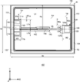
- FIG. 1B An example of the top view of the semiconductor device 100 according to the embodiment is shown.
- the enlarged view of the upper surface of the semiconductor device 100 is shown. It is a figure which shows an example of the aa'cross section in FIG. 1B. It is a figure for demonstrating the layout of the upper surface of the semiconductor device 100.
- the enlarged view of the upper surface of the semiconductor device 100 is shown.
- the enlarged view of the upper surface of the semiconductor device 100 is shown.
- the enlarged view of the upper surface of the semiconductor device 100 is shown.
- An example of the configuration of the semiconductor device 100 provided with the notch 118 is shown.
- An example of the configuration of the semiconductor device 100 provided with the notch 118 is shown. It is an example of the top view of the semiconductor device 100 provided with the protective film 180.
- one side in the direction parallel to the depth direction of the semiconductor substrate is referred to as "upper”, and the other side is referred to as “lower”.
- the upper surface is referred to as the upper surface and the other surface is referred to as the lower surface.
- the “up” and “down” directions are not limited to the direction of gravity or the direction when the semiconductor device is mounted.
- orthogonal coordinate axes of X-axis, Y-axis, and Z-axis Orthogonal axes only specify the relative positions of the components and do not limit a particular direction.
- the Z axis does not limit the height direction with respect to the ground.
- the + Z-axis direction and the ⁇ Z-axis direction are opposite to each other. When positive or negative is not described and is described as the Z-axis direction, it means the direction parallel to the + Z-axis and the -Z-axis.
- the orthogonal axes parallel to the upper surface and the lower surface of the semiconductor substrate are defined as the X axis and the Y axis. Further, the axis perpendicular to the upper surface and the lower surface of the semiconductor substrate is defined as the Z axis.
- the direction of the Z axis may be referred to as a depth direction. Further, in the present specification, the direction parallel to the upper surface and the lower surface of the semiconductor substrate including the X-axis and the Y-axis may be referred to as a horizontal direction.
- error When referred to as “same” or “equal” in the present specification, it may include a case where there is an error due to manufacturing variation or the like.
- the error is, for example, within 10%.
- the conductive type of the doping region doped with impurities is described as P-type or N-type.
- an impurity may mean, in particular, either an N-type donor or a P-type acceptor, and may be referred to as a dopant.
- doping means that a donor or acceptor is introduced into a semiconductor substrate to obtain a semiconductor showing an N-type conductive type or a semiconductor showing a P-type conductive type.
- the doping concentration means the concentration of a donor or the concentration of an acceptor in a thermal equilibrium state.
- the net doping concentration means the net concentration of the donor concentration as the concentration of positive ions and the acceptor concentration as the concentration of negative ions, including the polarity of the charge.
- the donor concentration is N D and the acceptor concentration is NA
- the net net doping concentration at any position is N D - NA .
- the net doping concentration may be simply referred to as a doping concentration.
- the donor has the function of supplying electrons to the semiconductor.
- the acceptor has a function of receiving electrons from a semiconductor.
- Donors and acceptors are not limited to the impurities themselves.
- the VOH defect to which the pores (V), oxygen (O) and hydrogen (H) present in the semiconductor are bonded functions as a donor for supplying electrons.
- VOH defects are sometimes referred to herein as hydrogen donors.
- P + type or N + type means that the doping concentration is higher than P type or N type
- P-type or N-type means that the doping concentration is higher than P-type or N-type. It means that the concentration is low.
- P ++ type or N ++ type in the present specification it means that the doping concentration is higher than that of P + type or N + type.
- the unit system of the present specification is an SI unit system unless otherwise specified. The unit of length may be displayed in cm or ⁇ m, but various calculations may be performed after converting to meters (m).
- FIG. 1A shows an example of a top view of the semiconductor device 100 according to the embodiment.
- the semiconductor device 100 is a semiconductor chip including a transistor unit 70 and a diode unit 80.
- the semiconductor device 100 may be mounted on a module such as an IPM (Intelligent Power Module).
- the transistor unit 70 is a region in which the semiconductor device 100 operates as a transistor.
- the transistor unit 70 includes a transistor such as an IGBT (Insulated Gate Bipolar Transistor).
- the diode unit 80 is a region in the semiconductor device 100 that performs a diode operation such as recirculating the current of the circuit.
- the diode section 80 includes a diode such as a freewheeling diode (FWD: Free Wheel Diode).
- the semiconductor device 100 of this example is a reverse conduction IGBT (RC-IGBT: Reverse Conducting IGBT) having a transistor portion 70 and a diode portion 80 on the same chip.
- the region of the transistor portion 70 may be indicated by the symbol I
- the region of the diode portion 80 may be indicated by the symbol F.
- the semiconductor substrate 10 may be a silicon substrate, a silicon carbide substrate, a nitride semiconductor substrate such as gallium nitride, or the like.
- the semiconductor substrate 10 of this example is a silicon substrate.
- the semiconductor substrate 10 has an active portion 102 and an outer peripheral portion 104.
- the outer peripheral end of the semiconductor substrate 10 in the top view is referred to as the outer peripheral end 150.
- the top view refers to a case where the semiconductor substrate 10 is viewed from the front surface side in a direction perpendicular to the front surface (Z-axis direction).
- the transistor portion 70 and the diode portion 80 may be alternately and periodically arranged periodically in the XY plane.
- the gate metal layer 50 may be provided above the semiconductor substrate 10.
- the transistor portion 70 and the diode portion 80 of this example have trench portions extending in the Y-axis direction and arranged in the X-axis direction.
- the transistor portion 70 and the diode portion 80 may have trench portions extending in the X-axis direction and arranged in the Y-axis direction.
- a boundary portion 90 and a boundary portion 92 which will be described later, may be provided in a region adjacent to the transistor portion 70 or the diode portion 80.
- the boundary portion 92 may be a region of the active portion 102 between the diode portion 80 and the gate metal layer 50 in a top view.
- the boundary portion 92 of this example is provided in the region between the diode portion 80 and the gate metal layer 50 in the Y-axis direction, and is provided between the transistor portions 70 in the X-axis direction.
- a collector region 22 described later may be provided on the back surface of the semiconductor substrate 10.
- the active unit 102 has a transistor unit 70 and a diode unit 80.
- the active portion 102 is a region in which a main current flows between the front surface and the back surface of the semiconductor substrate 10 when the semiconductor device 100 is controlled to be in the ON state. That is, it is a region in which a current flows in the depth direction inside the semiconductor substrate 10 from the front surface to the back surface of the semiconductor substrate 10 or from the back surface to the front surface.
- the transistor unit 70 and the diode unit 80 are referred to as element units or element regions, respectively.
- the region sandwiched between the two element portions is also referred to as the active portion 102.
- the active portion 102 also includes a region sandwiched between the element portions and provided with the gate metal layer 50.
- the gate metal layer 50 is formed of a material containing metal.
- the gate metal layer 50 is formed of aluminum, an aluminum-silicon alloy, or an aluminum-silicon-copper alloy.
- the gate metal layer 50 is electrically connected to the gate conductive portion of the transistor portion 70, and supplies a gate voltage to the transistor portion 70.
- the gate metal layer 50 is provided so as to surround the outer periphery of the active portion 102 in a top view.
- the gate metal layer 50 is electrically connected to the gate pad 122 provided on the outer peripheral portion 104.
- the gate metal layer 50 may be provided along the outer peripheral edge 150 of the semiconductor substrate 10. Further, the gate metal layer 50 may be provided around the temperature sense portion 140 or between the transistor portion 70 and the diode portion 80 in a top view.
- the gate metal layer 50 of this example is shown by a thick line.
- the outer peripheral portion 104 is a region between the active portion 102 and the outer peripheral end 150 of the semiconductor substrate 10 in a top view.
- the outer peripheral portion 104 is provided so as to surround the active portion 102 in a top view.
- On the outer peripheral portion 104 one or more metal pads for connecting the semiconductor device 100 and the external device with a wire or the like may be arranged.
- the outer peripheral portion 104 may have an edge termination structure portion.
- the edge terminal structure portion relaxes the electric field concentration on the front surface side of the semiconductor substrate 10.
- the edge termination structure has a guard ring, a field plate, a resurf, and a combined structure thereof.
- the front surface electrode is provided above the semiconductor substrate 10.
- the front surface electrode includes an emitter electrode 52 described later.
- the front surface electrode may include a first control pad 110 and a second control pad 120.
- the front surface electrode may be connected to an external electrode of the semiconductor device 100 by wire bonding or the like. The number and positions of the front surface electrodes are not limited to this example.
- the first control pad 110 is provided so as to project from the predetermined outer peripheral edge 151 of the semiconductor substrate 10 to the inside of the semiconductor substrate 10 in a top view.
- the fact that the first control pad 110 projects from the first outer peripheral 151 to the inside of the semiconductor substrate 10 means that the outer peripheral portion 104 is extended and provided inside the active portion 102. That is, the active portion 102 is provided on the positive side or the negative side of the first control pad 110 in the Y-axis direction.
- the first control pad 110 of this example includes an anode pad 112, a cathode pad 114, and a sense pad 116.
- the second control pad 120 is provided so as to project from the second outer peripheral 152 to the inside of the semiconductor substrate 10 in a top view.
- the second outer peripheral 152 is the side of the outer peripheral end 150 facing the first outer peripheral 151.
- the first outer periphery 151 and the second outer periphery 152 of this example are parallel to the stretching direction of the trench portion (in this example, the Y-axis direction) in the top view.
- the second control pad 120 of this example includes a gate pad 122.
- the well region 115 is provided below the first control pad 110 and covers the first control pad 110 in a top view.
- the well region 115 of this example has a rectangular shape when viewed from above, and three sides of the well region 115 are provided so as to face the active portion 102.
- the well region 115 has a corner portion 111 provided so as to project from the first outer periphery 151.
- the well region 125 is provided below the second control pad 120 and covers the second control pad 120 in a top view.
- the well region 125 of this example has a rectangular shape in a top view, and three sides of the well region 125 are provided so as to face the active portion 102.
- the well region 125 has a corner portion 121 provided so as to project from the second outer peripheral 152.
- the well region 135 is provided so as to cover the gate metal layer 50 in a top view.
- the well region 135 of this example is provided along the outer peripheral portion 104 so as to cover the gate metal layer 50.
- the well region 135 may be connected to the well region 115.
- the well region 145 is provided so as to cover the gate metal layer 50 in a top view.
- the well region 145 of this example may be provided so as to further cover the temperature sense unit 140 and the temperature sense wiring 142.
- the well region 145 may be connected to the well region 115 and the well region 125.
- the well region 115, the well region 125, the well region 135, and the well region 145 are second conductive type regions provided on the front surface side of the semiconductor substrate 10.
- the conductive type of the well region 115, the well region 125, the well region 135 and the well region 145 is a P + type as an example.
- the gate pad 122 is electrically connected to the gate metal layer 50.
- the gate pad 122 is electrically connected to the gate conductive portion of the transistor portion 70 via the gate metal layer 50.
- the gate pad 122 is set to the gate potential.
- the gate pad 122 of this example is rectangular in top view. In one example, the gate pad 122 may have one side of 1000 ⁇ m or more and 1500 ⁇ m or less, but is not limited thereto.
- the anode pad 112 is electrically connected to the anode region of the temperature sense unit 140.
- the anode pad 112 is electrically connected to the anode region of the temperature sense unit 140 by the temperature sense wiring 142.
- the anode pad 112 of this example is rectangular in top view.
- the anode pad 112 may have a short side of 500 ⁇ m or more and 900 ⁇ m or less and a long side of 1000 ⁇ m or more and 1500 ⁇ m or less, but is not limited thereto.
- the cathode pad 114 is electrically connected to the cathode region of the temperature sense unit 140.
- the cathode pad 114 is electrically connected to the cathode region of the temperature sense unit 140 by the temperature sense wiring 142.
- the cathode pad 114 of this example is rectangular in top view.
- the cathode pad 114 may have the same shape as the anode pad 112 when viewed from above.
- the temperature sense unit 140 is arranged above the active unit 102 and detects the temperature of the semiconductor substrate 10.
- the temperature sense unit 140 of this example detects the temperature of the active unit 102.
- the temperature sense unit 140 may have a diode formed of a semiconductor material such as polysilicon.
- the temperature sense unit 140 is used to detect the temperature of the semiconductor device 100 and protect the semiconductor chip from overheating.
- the temperature sense unit 140 has a longitudinal length in the X-axis direction and a short hand in the Y-axis direction, but is not limited thereto.
- the temperature sense unit 140 of this example is provided near the center of the active unit 102 in a top view.
- the temperature sense unit 140 may be provided in any region of the transistor unit 70 and the diode unit 80. That is, a second conductive type collector region or a first conductive type cathode region may be provided on the back surface side of the semiconductor substrate 10 provided with the temperature sense unit 140.
- the temperature sense wiring 142 electrically connects the anode pad 112 and the cathode pad 114 to the temperature sense unit 140.
- the temperature sense wiring 142 is provided above the active portion 102 so as to extend from the temperature sense portion 140 to the outer peripheral portion 104.
- the temperature sense wiring 142 may be made of the same material as the front surface electrode. In top view, a P + type well region may be arranged in the region of the semiconductor substrate 10 that overlaps the temperature sense portion 140 and the temperature sense wiring 142.
- FIG. 1B shows an enlarged view of the upper surface of the semiconductor device 100.
- an enlarged view of the region A of FIG. 1A is shown.
- the transistor portion 70 may be a region in which a collector region 22 provided on the back surface side of the semiconductor substrate 10 is projected onto the front surface of the semiconductor substrate 10.
- the collector region 22 has a second conductive type.
- the collector area 22 of this example is a P + type as an example.
- the transistor portion 70 includes a boundary portion 90 located at the boundary between the transistor portion 70 and the diode portion 80.
- the diode portion 80 may be a region in which the cathode region 82 provided on the back surface side of the semiconductor substrate 10 is projected onto the front surface of the semiconductor substrate 10.
- the cathode region 82 has a first conductive type.
- the cathode region 82 of this example is N + type as an example.
- the semiconductor device 100 of this example has a gate trench portion 40, a dummy trench portion 30, an emitter region 12, a base region 14, a contact region 15, and a well region 145 on the front surface of the semiconductor substrate 10. Be prepared. Further, the semiconductor device 100 of this example includes an emitter electrode 52 and a gate metal layer 50 provided above the front surface of the semiconductor substrate 10.
- the emitter electrode 52 is provided above the gate trench portion 40, the dummy trench portion 30, the emitter region 12, the base region 14, the contact region 15 and the well region 145. Further, the gate metal layer 50 is provided above the gate trench portion 40 and the well region 145.
- the emitter electrode 52 and the gate metal layer 50 are formed of a material containing metal.
- the emitter electrode 52 may be formed of aluminum, aluminum-silicon alloy, or aluminum-silicon-copper alloy.
- the emitter electrode 52 may have a barrier metal formed of titanium, a titanium compound, or the like in the lower layer of a region formed of aluminum or the like.
- the emitter electrode 52 and the gate metal layer 50 are provided separately from each other.
- the emitter electrode 52 and the gate metal layer 50 are provided above the semiconductor substrate 10 with the interlayer insulating film 38 interposed therebetween.
- the interlayer insulating film 38 is omitted in FIG. 1A.
- the interlayer insulating film 38 is provided with a contact hole 54, a contact hole 55, and a contact hole 56 penetrating.
- the contact hole 55 connects the gate metal layer 50 and the gate conductive portion in the transistor portion 70.
- a plug made of tungsten or the like may be formed inside the contact hole 55.
- the contact hole 56 connects the emitter electrode 52 and the dummy conductive portion in the dummy trench portion 30.
- a plug made of tungsten or the like may be formed inside the contact hole 56.
- the connecting portion 25 electrically connects the front surface electrode such as the emitter electrode 52 or the gate metal layer 50 with the conductive portion formed inside the trench portion.
- the connecting portion 25 is provided between the gate metal layer 50 and the gate conductive portion.
- the connecting portion 25 is also provided between the emitter electrode 52 and the dummy conductive portion.
- the connection portion 25 contains a conductive material such as polysilicon doped with impurities.
- the connection portion 25 of this example is polysilicon (N +) doped with N-type impurities.
- the connecting portion 25 is provided above the front surface of the semiconductor substrate 10 via an insulating film such as an oxide film.
- the gate trench portions 40 are arranged at predetermined intervals along a predetermined arrangement direction (X-axis direction in this example).
- the gate trench portion 40 of this example has two stretched portions 41 and 2 that are parallel to the front surface of the semiconductor substrate 10 and stretched along a stretch direction (Y-axis direction in this example) perpendicular to the arrangement direction. It may have a connecting portion 43 connecting the two stretched portions 41.
- the gate trench portion 40 is set to the gate potential.
- the connecting portion 43 is formed in a curved shape.
- the dummy trench portion 30 is a trench portion electrically connected to the emitter electrode 52. Similar to the gate trench portion 40, the dummy trench portions 30 are arranged at predetermined intervals along a predetermined arrangement direction (in this example, the X-axis direction). Like the gate trench portion 40, the dummy trench portion 30 of this example may have a U-shape on the front surface of the semiconductor substrate 10. That is, the dummy trench portion 30 may have two stretching portions 31 that stretch along the stretching direction and a connecting portion 33 that connects the two stretching portions 31.
- the transistor portion 70 of this example has a structure in which two gate trench portions 40 and three dummy trench portions 30 are repeatedly arranged. That is, the transistor portion 70 of this example has a gate trench portion 40 and a dummy trench portion 30 at a ratio of 2: 3. For example, the transistor portion 70 has one stretched portion 31 between the two stretched portions 41. Further, the transistor portion 70 has two extending portions 31 adjacent to the gate trench portion 40.
- the ratio of the gate trench portion 40 and the dummy trench portion 30 is not limited to this example.
- the ratio of the gate trench portion 40 to the dummy trench portion 30 may be 1: 1 or 2: 4.
- the transistor portion 70 may have a so-called full gate trench structure (all-gate trench structure) in which the dummy trench portion 30 is not provided and all the gate trench portions 40 are used.
- the well region 145 is a second conductive type region provided on the front surface side of the semiconductor substrate 10 with respect to the drift region 18 described later.
- the well region 145 is an example of a well region provided on the edge side of the semiconductor device 100.
- the well region 145 is P + type as an example.
- the well region 145 is formed in a predetermined range from the end of the active region on the side where the gate metal layer 50 is provided.
- the diffusion depth of the well region 145 may be deeper than the depth of the gate trench portion 40 and the dummy trench portion 30. A part of the gate trench portion 40 and the dummy trench portion 30 on the gate metal layer 50 side is formed in the well region 145.
- the bottom of the extending end of the gate trench 40 and the dummy trench 30 may be covered by the well region 145.
- the well region 145 may be formed at the same time as the well region 115 and the well region 125.
- the well areas 115, well areas 125, well areas 135 and well areas 145 may have the same or substantially the same diffusion depth.
- the well region 145 may be provided so as to cover the gate metal layer 50 in a top view.
- the well region 145 may be electrically connected to the emitter electrode 52 at a position closer to the outer peripheral portion 104 on the outer peripheral side than the transistor portion 70 or the diode portion 80.
- the contact hole 54 is a portion where the interlayer insulating film 38 is opened to expose the front surface 21 of the semiconductor substrate 10.
- the contact hole 54 is formed in the transistor portion 70 above each region of the emitter region 12 and the contact region 15. Through the contact hole 54, the emitter region 12 or the contact region 15 comes into contact with the emitter electrode 52 and is electrically connected.
- the contact hole 54 is provided above the base region 14.
- the base region 14 in the diode portion 80 may be in contact with the emitter electrode 52 via the contact hole 54.
- the same conductive high-concentration layer as the base region 14 may be provided between the base region 14 and the emitter electrode 52 in order to reduce the contact resistance. ..
- the contact hole 54 is provided above the contact region 15.
- the contact holes 54 may not be provided above the well regions 145 provided at both ends in the Y-axis direction.
- one or a plurality of contact holes 54 are formed in the interlayer insulating film 38.
- the one or more contact holes 54 may be provided by being stretched in the stretching direction.
- the boundary portion 90 is provided in the transistor portion 70 and is a region adjacent to the diode portion 80.
- the boundary portion 90 may have a contact region 15.
- the boundary portion 90 of this example does not have an emitter region 12.
- the trench portion of the boundary portion 90 is a dummy trench portion 30.
- the boundary portion 90 of this example is arranged so that both ends in the X-axis direction are dummy trench portions 30.
- the mesa portion 71, the mesa portion 91, and the mesa portion 81 are the mesa portions provided adjacent to the trench portion in the plane parallel to the front surface of the semiconductor substrate 10.
- the mesa portion is a portion of the semiconductor substrate 10 sandwiched between two adjacent trench portions, and may be a portion from the front surface of the semiconductor substrate 10 to the depth of the deepest bottom of each trench portion. ..
- the extended portion of each trench portion may be used as one trench portion. That is, the region sandwiched between the two stretched portions may be the mesa portion.
- the mesa portion 71 is provided adjacent to at least one of the dummy trench portion 30 or the gate trench portion 40 in the transistor portion 70.
- the mesa portion 71 may have an emitter region 12, a base region 14, a contact region 15, and a well region 145 on the front surface of the semiconductor substrate 10.
- the emitter region 12 and the contact region 15 may be provided alternately in the stretching direction.
- the mesa portion 91 is provided at the boundary portion 90.
- the mesa portion 91 may have a contact region 15 or a well region 145 on the front surface of the semiconductor substrate 10.
- the mesa portion 81 is provided in the diode portion 80 in a region sandwiched between adjacent dummy trench portions 30.
- the mesa portion 81 may have a base region 14 and a contact region 15 or a well region 145 on the front surface of the semiconductor substrate 10.
- the base region 14 is a second conductive type region provided on the front surface side of the semiconductor substrate 10 in the transistor portion 70 and the diode portion 80.
- the base region 14 is P-type as an example.
- the base region 14 may be provided at both ends of the mesa portion 71 and the mesa portion 91 in the Y-axis direction on the front surface of the semiconductor substrate 10. Note that FIG. 1A shows only one end of the base region 14 in the Y-axis direction.
- the base region 14 may have a lower doping concentration than the well region 145.
- the emitter region 12 is a first conductive type region having a higher doping concentration than the drift region 18.
- the emitter region 12 of this example is N + type as an example.
- An example of a dopant in the emitter region 12 is arsenic (As).
- the emitter region 12 is provided in contact with the gate trench portion 40 on the front surface of the mesa portion 71.
- the emitter region 12 may be provided so as to extend in the X-axis direction from one of the two trench portions sandwiching the mesa portion 71 to the other.
- the emitter region 12 is also provided below the contact hole 54.
- the emitter region 12 may or may not be in contact with the dummy trench portion 30.
- the emitter region 12 of this example is in contact with the dummy trench portion 30.
- the emitter region 12 does not have to be provided in the mesa portion 91 of the boundary portion 90.
- the contact region 15 is a second conductive type region having a higher doping concentration than the base region 14.
- the contact region 15 of this example is a P + type as an example.
- the thickness of the contact region 15 in the depth direction may be thinner than the thickness of the base region 14 in the depth direction.
- the contact region 15 of this example is provided on the front surface of the mesa portion 71 and the mesa portion 91.
- the contact region 15 may be provided in the X-axis direction from one of the two trench portions sandwiching the mesa portion 71 or the mesa portion 91 to the other.
- the contact region 15 may or may not be in contact with the gate trench portion 40. Further, the contact region 15 may or may not be in contact with the dummy trench portion 30. In this example, the contact region 15 is in contact with the dummy trench portion 30 and the gate trench portion 40.
- the contact area 15 is also provided below the contact hole 54.
- the contact region 15 may also be provided in the mesa portion 81.
- the trench length Lt is the length of a plurality of trench portions in the stretching direction.
- the trench length Lt of this example is the distance between the gate metal layer 50 provided on the positive side of the trench portion in the Y-axis direction and the gate metal layer 50 provided on the negative side of the trench portion in the Y-axis direction.
- the trench length Lt may be 2000 ⁇ m or more, 3000 ⁇ m or more, 4000 ⁇ m or more, 4600 ⁇ m or more, and 6000 ⁇ m or more. Further, the trench length Lt may be 50,000 ⁇ m or less, 30,000 ⁇ m or less, and 20,000 ⁇ m or less.
- FIG. 1C is a diagram showing an example of a'a'cross sections in FIG. 1B.
- the aa'cross section is an XZ plane that passes through the emitter region 12 in the transistor portion 70.
- the semiconductor device 100 of this example has a semiconductor substrate 10, an interlayer insulating film 38, an emitter electrode 52, and a collector electrode 24 in the aa'cross section.
- the emitter electrode 52 is formed above the semiconductor substrate 10 and the interlayer insulating film 38.
- the drift region 18 is a first conductive type region provided on the semiconductor substrate 10.
- the drift region 18 of this example is N-type as an example.
- the drift region 18 may be a region remaining in the semiconductor substrate 10 without forming another doping region. That is, the doping concentration of the drift region 18 may be the doping concentration of the semiconductor substrate 10.
- the buffer region 20 is a first conductive type region provided below the drift region 18.
- the buffer area 20 of this example is N-type as an example.
- the doping concentration in the buffer region 20 is higher than the doping concentration in the drift region 18.
- the buffer region 20 may function as a field stop layer that prevents the depletion layer extending from the back surface side of the base region 14 from reaching the collector region 22 of the second conductive type and the cathode region 82 of the first conductive type.
- the collector area 22 is provided below the buffer area 20 in the transistor unit 70.
- the cathode region 82 is provided below the buffer region 20 in the diode portion 80.
- the boundary between the collector region 22 and the cathode region 82 may be the boundary between the transistor portion 70 and the diode portion 80.
- the collector electrode 24 is formed on the back surface 23 of the semiconductor substrate 10.
- the collector electrode 24 is made of a conductive material such as metal.
- the base region 14 is a second conductive type region provided above the drift region 18 in the mesa portion 71, the mesa portion 91, and the mesa portion 81.
- the base region 14 may be provided in contact with the gate trench portion 40.
- the base region 14 may be provided in contact with the dummy trench portion 30.
- the emitter region 12 is provided between the base region 14 and the front surface 21 in the mesa portion 71.
- the emitter region 12 may be provided in contact with the gate trench portion 40.
- the emitter region 12 may or may not be in contact with the dummy trench portion 30.
- the emitter region 12 does not have to be provided in the mesa portion 91.
- the contact region 15 is provided above the base region 14 in the mesa portion 91.
- the contact region 15 is provided in the mesa portion 91 in contact with the gate trench portion 40.
- the contact region 15 may be provided on the front surface 21 of the mesa portion 71.
- the storage region 16 is a first conductive type region provided on the front surface 21 side of the semiconductor substrate 10 with respect to the drift region 18.
- the storage area 16 of this example is N + type as an example.
- the donor concentration in the accumulation region 16 is higher than the donor concentration in the drift region 18.
- the storage region 16 is provided in the transistor portion 70 and the diode portion 80.
- the storage area 16 of this example is also provided at the boundary portion 90. As a result, the semiconductor device 100 can avoid the mask shift of the storage region 16.
- the storage area 16 is provided in contact with the gate trench portion 40.
- the storage region 16 may or may not be in contact with the dummy trench portion 30.
- the doping concentration of the accumulation region 16 is higher than the doping concentration of the drift region 18.
- One or more gate trench portions 40 and one or more dummy trench portions 30 are provided on the front surface 21.
- Each trench portion is provided from the front surface 21 to the drift region 18.
- each trench portion also penetrates these regions and reaches the drift region 18.
- the fact that the trench portion penetrates the doping region is not limited to those manufactured in the order of forming the doping region and then forming the trench portion. Those in which the doping region is formed between the trench portions after the trench portion is formed are also included in those in which the trench portion penetrates the doping region.
- the gate trench portion 40 has a gate trench formed on the front surface 21, a gate insulating film 42, and a gate conductive portion 44.
- the gate insulating film 42 is formed so as to cover the inner wall of the gate trench.
- the gate insulating film 42 may be formed by oxidizing or nitriding the semiconductor on the inner wall of the gate trench.
- the gate conductive portion 44 is formed inside the gate trench and inside the gate insulating film 42.
- the gate insulating film 42 insulates the gate conductive portion 44 and the semiconductor substrate 10.
- the gate conductive portion 44 is formed of a conductive material such as polysilicon.
- the gate trench portion 40 is covered with an interlayer insulating film 38 on the front surface 21.
- the gate conductive portion 44 includes a region facing the adjacent base region 14 on the mesa portion 71 side with the gate insulating film 42 interposed therebetween in the depth direction of the semiconductor substrate 10.
- a predetermined voltage is applied to the gate conductive portion 44, a channel due to an electron inversion layer is formed on the surface layer of the interface in the base region 14 in contact with the gate trench.
- the width of the gate trench portion 40 may be larger than 0.5 ⁇ m and smaller than 2.0 ⁇ m.
- the width of the gate trench portion 40 of this example is 1.0 ⁇ m.
- the thickness of the gate insulating film 42 may be thicker than 0.05 ⁇ m and thinner than 0.2 ⁇ m.
- the thickness of the gate insulating film 42 of this example is 0.1 ⁇ m.
- the width Wg of the gate conductive portion 44 may be obtained by subtracting the thickness of the gate insulating film 42 (that is, two layers of the gate insulating film 42) from the width of the gate trench portion 40.
- the width of the gate trench portion 40 may be constant in the depth direction, may be increased, or may be decreased.
- the width Wg of the gate conductive portion 44 may be the width of the gate conductive portion 44 at the same depth position as the depth at which the doping concentration peaks in the base region 14.
- the width Wg of the gate conductive portion 44 may be the width of the gate conductive portion 44 at the depth at which the base region 14 is in contact with the emitter region 12, that is, the pn junction depth.
- the dummy trench portion 30 may have the same structure as the gate trench portion 40.
- the dummy trench portion 30 has a dummy trench formed on the front surface 21 side, a dummy insulating film 32, and a dummy conductive portion 34.
- the dummy insulating film 32 is formed so as to cover the inner wall of the dummy trench.
- the dummy conductive portion 34 is formed inside the dummy trench and inside the dummy insulating film 32.
- the dummy insulating film 32 insulates the dummy conductive portion 34 and the semiconductor substrate 10.
- the dummy trench portion 30 is covered with the interlayer insulating film 38 on the front surface 21.
- the interlayer insulating film 38 is provided on the front surface 21.
- An emitter electrode 52 is provided above the interlayer insulating film 38.
- the interlayer insulating film 38 is provided with one or a plurality of contact holes 54 for electrically connecting the emitter electrode 52 and the semiconductor substrate 10. Similarly, the contact hole 55 and the contact hole 56 may be provided so as to penetrate the interlayer insulating film 38.
- the lifetime control region 130 may be provided on the front surface 21 side of the semiconductor substrate 10 in the diode portion 80.
- the front surface 21 side of the semiconductor substrate 10 may refer to a region on the front surface 21 side of the semiconductor substrate 10 in the depth direction with respect to the center. Further, when the lifetime control regions are provided at different depth positions of the semiconductor substrate 10, the lifetime control region on the front surface 21 side may be the lifetime control region 130.
- the lifetime control region 130 may be a region in which a lifetime killer is intentionally introduced by injecting impurities into the semiconductor substrate 10 or the like.
- the lifetime value of the electron or hole carrier in the region where the lifetime killer is intentionally introduced is smaller than the lifetime of the carrier in the region where the lifetime killer is not intentionally introduced.
- the lifetime killer is a carrier recombination center, may be a lattice defect, and is a dangling bond formed by vacancies, double vacancies, vacancies, etc., and these and elements constituting the semiconductor substrate 10. It may be a compound defect or a dislocation.
- the lifetime killer may be a noble gas element such as helium or neon or a hydrogen element, or may be a transition metal such as platinum or gold.
- the lifetime control region 130 may be formed by electron beam irradiation.
- the lifetime killer is approximately one from the front surface 21 to the back surface 23 regardless of whether the semiconductor substrate 10 is irradiated from the front surface 21 or the back surface 23.
- the distribution is similar. However, if an arbitrary position on the front surface 21 side is considered as the lifetime control area 130, the same argument as other lifetime killer holds.
- the lifetime control area 130 of this example is also provided at the boundary portion 90. As a result, it is possible to suppress the flow of holes from the base region 14 of the transistor portion 70 to the cathode region 82 of the diode portion 80 during the reverse recovery of the diode portion 80, and it is possible to reduce the reverse recovery loss.
- the lifetime control area 130 may be terminated in the middle of the boundary portion 90 and may not be provided in the entire boundary portion 90.
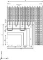
- FIG. 1D is a diagram for explaining the layout of the upper surface of the semiconductor device 100. In FIG. 1D, some configurations are omitted in order to explain the structure of the semiconductor device 100.
- the central virtual line VL is orthogonal to the first outer peripheral 151 and passes through the center of the first outer peripheral 151.
- the central virtual line VL of this example is a virtual line that passes through the center of the semiconductor substrate 10 in the Y-axis direction and extends in the X-axis direction.
- the distance Ha is the length of the semiconductor substrate 10 in the direction orthogonal to the central virtual line VL, and corresponds to the lengths of the first outer peripheral 151 and the second outer peripheral 152.
- the distance Hb is the length of the semiconductor substrate 10 in the direction parallel to the central virtual line VL.
- the distance Hb in this example is longer than the distance Ha, but may be the same as the distance Ha, or may be shorter than the distance Ha.
- the distance Hc is the distance from the central virtual line VL to the outer peripheral end 150 of the semiconductor substrate 10 in the direction orthogonal to the central virtual line VL. That is, the distance Hc is half the length of the distance Ha.
- the well region 115 includes two corners, a corner 111a and a corner 111b.
- the corner portions 111a and the corner portions 111b are provided in regions opposite to each other with the central virtual line VL interposed therebetween.
- the corner portion farther from the central virtual line VL is referred to as a corner portion 111a, and the corner portion closer to the central virtual line VL is referred to as a corner portion 111b.
- the distance L1a is the distance in the extending direction from the central virtual line VL to the corner portion 111a.
- the distance L1a of this example is the distance to the corner portion 111a away from the central virtual line VL in the well region 115 provided asymmetrically.
- the distance L1b is the distance in the extending direction from the central virtual line VL to the corner portion 111b.
- the distance L1a may be the same as or different from the distance L1b.
- the distance L1a in this example is larger than the distance L1b. That is, the well region 115 of this example is provided asymmetrically with respect to the central virtual line VL.
- the distance L1a may be 30% or more of the distance Hc, or may be 40% or more.
- the distance L1a may be 90% or less of the distance Hc, and may be 80% or less.
- the well region 125 includes two corners, a corner 121a and a corner 121b.
- the corner portion on the side provided with the corner portion 111a is referred to as the corner portion 121a
- the corner portion on the side provided with the corner portion 111b is referred to as the corner portion 121b. That is, the corner portion 121b is provided on the opposite side of the corner portion 121a with the central virtual line VL interposed therebetween.
- the corner portion 111a, the corner portion 111b, the corner portion 121a, and the corner portion 121b are shown at right angles in FIG. 1D, the tip of the corner portion may be curved. Alternatively, the corner of the tip of the corner may be dropped to form a polygonal shape. This makes it possible to suppress an increase in the electric field strength at the corners. The same may be applied to the other corners of the well region 125. The same applies to the corner portions 111 after this example.
- the distance L2a is the distance in the extending direction from the central virtual line VL to the corner portion 121a.
- the distance L2b is the distance in the extending direction from the central virtual line VL to the corner portion 121b.
- the distance L2a in this example is equal to the distance L2b. That is, the well region 125 is provided symmetrically with respect to the central virtual line VL.
- the distance L1a may be longer or shorter than the distance L2a.
- the shortest distance R1a is the shortest distance between the well region 115 and the trench center position TP in the top view.
- the trench center position TP is the center position of the trench length Lt of the plurality of trench portions.
- the shortest distance R1a may be the shortest distance between the corner portion 111a and the trench center position TP. When the distance L1a is increased, the shortest distance R1a becomes shorter, and the corner portion 111a approaches the trench center position TP.
- the shortest distance R1a may be 1000 ⁇ m or more, 1500 ⁇ m or more, and 2000 ⁇ m or more.
- the current filament is likely to be generated near the trench center position TP due to the delay of the gate.
- the trench length Lt becomes longer, the operating area can be increased and a large current can be controlled. Therefore, by setting the shortest distance R1a in an appropriate range, it is possible to avoid element destruction even with a long trench length Lt.
- the ratio obtained by dividing the trench length Lt by the width Wg is defined as the conductive portion shape ratio ⁇ .
- the conductive portion shape ratio ⁇ may be 1000 or more, may be 3000 or more, may be 5000 or more, and may be 6000 or more.
- the conductive portion shape ratio ⁇ may be 1 ⁇ 106 or less, may be 3 ⁇ 105 or less, may be 1 ⁇ 105 or less, and may be 50,000 or less. If the conductive portion shape ratio ⁇ in these ranges, the trench length Lt may be in the above range or may be out of the range.
- the mesa width in the arrangement direction may be smaller than the width in the arrangement direction of the gate trench portion 40.
- the conductive portion shape ratio ⁇ may be determined by comprehensively considering the delay time generated in the charging / discharging of the gate in addition to the current characteristics. In the semiconductor device 100 of this example, by appropriately setting the shortest distance R1a, element destruction can be avoided even with a long trench length Lt, so that a wider range of conductive portion shape ratio ⁇ can be adopted. ..
- the value of the conductive portion shape ratio ⁇ may be used in combination with any of the values of the shortest distance R1a, the shortest distance R1b, the shortest distance R2a, and the shortest distance R2b disclosed in this example.
- the shortest distance R1b is the shortest distance between the well region 115 and the trench center position TP of the active portion 102 adjacent to the well region 115 in the stretching direction.
- the shortest distance R1b in this example is longer than the shortest distance R1a.
- the shortest distance R1b may be 1000 ⁇ m or more, 1500 ⁇ m or more, and 2000 ⁇ m or more.
- the shortest distance R2a is the shortest distance between the well region 125 in the top view and the trench center position TP of the active portion 102 adjacent to the well region 125 in the stretching direction.
- the shortest distance R2a may be the shortest distance between the corner portion 121a and the trench center position TP.
- the shortest distance R2a may be 1000 ⁇ m or more, 1500 ⁇ m or more, and 2000 ⁇ m or more.
- the shortest distance R2b is the shortest distance between the well region 125 and the trench center position TP of the active portion 102 adjacent to the well region 125 in the stretching direction.
- the shortest distance R2b in this example is longer than the shortest distance R2a.
- the shortest distance R2b may be 1000 ⁇ m or more, 1500 ⁇ m or more, and 2000 ⁇ m or more.
- the inflow of the current filament into the P-shaped well region can be suppressed by setting the shortest distance R1a and the shortest distance R2a to 1500 ⁇ m or more. As a result, it is possible to avoid element destruction in the vicinity of the P-shaped well region, so that the turn-off resistance can be improved.
- FIG. 2A shows an enlarged view of the upper surface of the semiconductor device 100.
- an enlarged view of the region B of FIG. 1A is shown.
- the corner portion 111 of this example is located at the transistor portion 70 in the top view.
- the position at the transistor portion 70 may mean that the corner portion 111 is provided at the mesa portion 71 sandwiched between the gate trench portions 40.
- a gate trench 40 may be provided above the well region 115.
- the corner portion 111 of this example is adjacent to the base region 14 of the transistor portion 70.
- the gate trench portion 40 is provided by extending to the gate metal layer 50.
- the gate metal layer 50 is provided along the outer circumference of the well region 115, but is not limited thereto.
- FIG. 2B shows an enlarged view of the upper surface of the semiconductor device 100.
- the semiconductor device 100 of this example is an example in which the corner portion 111 is provided in the dummy trench region 172.
- the dummy trench region 172 is a region in which a plurality of trench portions are set to the emitter potential.
- the dummy trench region 172 of this example includes a dummy trench portion 30 set to the emitter potential.
- the dummy trench region 172 of this example includes a mesa portion 71 in which the emitter region 12 and the contact region 15 are alternately arranged.
- the dummy trench region 172 may or may not be provided with the emitter region 12. Since the current is not turned on and off by the gate trench portion 40 in the dummy trench region 172, the main current does not flow. Therefore, in the dummy trench region 172, the concentration of the main current on the front surface 21 is small.
- the corner portion 111 is located in the dummy trench region 172 in the top view.
- the fact that the corner portion 111 is located in the dummy trench region 172 may mean that the trench portion closest to the corner portion 111 is the dummy trench portion 30. Further, the fact that the corner portion 111 is located in the dummy trench region 172 may mean that at least one dummy trench portion 30 is provided between the corner portion 111 and the gate trench portion 40.
- the corner portion 111 of this example is provided adjacent to the base region 14 between two adjacent dummy trench portions 30.
- the semiconductor device 100 of this example can suppress the current concentration in the vicinity of the corner portion 111 by covering the vicinity of the corner portion 111 with the dummy trench region 172.
- FIG. 2C shows an enlarged view of the upper surface of the semiconductor device 100.
- the semiconductor device 100 of this example is an example in which the corner portion 111 is provided in the diode portion 80.
- the dummy trench portion 30 is provided so as to extend to the inside of the well region 115. That is, the negative end portion of the dummy trench portion 30 in the Y-axis direction is located in the well region 115.
- the corner portion 111 is located at the diode portion 80 in the top view.
- the corner portion 111 of this example is provided adjacent to the base region 14 between two adjacent dummy trench portions 30.
- the current concentration in the vicinity of the corner portion 111 can be suppressed by covering the vicinity of the corner portion 111 with the diode portion 80.
- FIG. 2D shows an example of the configuration of the semiconductor device 100 including the notch 118.
- the notch 118 of this example is provided in the well region 115.
- the corner portion 111 of this example is located at the transistor portion 70 in the top view.
- the notch 118 is a region in which a part of the corner of the well region 115 is cut off in the top view.
- the notch 118 of this example has a shape in which the corner of the well region 115 is cut off on an arc, but the shape of the notch 118 is not limited to this example.
- the outermost protruding position on the arc of the notch 118 may be the corner 111.
- the notch length N1 is the distance connecting the ends of the region where the notch 118 is formed in the well region 115.
- the notch length N1 may be 10 ⁇ m or more, 30 ⁇ m or more, 50 ⁇ m or more, and 100 ⁇ m or more.
- the notch length N1 may be 1000 ⁇ m or less, 500 ⁇ m or less, and 200 ⁇ m or less. In one example, the notch length N1 is 100 ⁇ m.
- the radius of curvature of the notch 118 may be 10 ⁇ m or more, 20 ⁇ m or more, 50 ⁇ m or more, and 100 ⁇ m or more.
- the radius of curvature of the notch 118 may be 1000 ⁇ m or less, 500 ⁇ m or less, and 200 ⁇ m or less.
- FIG. 2E shows an example of the configuration of the semiconductor device 100 provided with the notch 118.
- the notch 118 of this example is provided in the well region 115.
- the corner portion 111 of this example is located at the diode portion 80 in the top view.
- the shape of the notch 118 may be similar to that of the embodiment of FIG. 2D. Since the cutout portion 118 of this example is located in the diode portion 80, it becomes easier to further increase the distance between the well region 115 and the trench center position TP, and it becomes easier to avoid the destruction of the semiconductor device 100.
- the corner portion 121 of the well region 125 may be located in the transistor portion 70, may be located in the dummy trench region 172, or may be located in the diode portion 80.
- the corner portion 111 of FIGS. 2A to 2E may be either the corner portion 111a or the corner portion 111b.
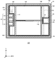
- FIG. 3 is an example of a top view of the semiconductor device 100 provided with the protective film 180.
- the semiconductor device 100 of this example includes an invalid region 170.
- the invalid area 170 is an area that does not function as the transistor unit 70.
- the invalid region 170 may be a dummy trench region 172 or a diode portion 80.
- the invalid region 170 of this example is also provided around the corner portion 121, and can suppress the inflow of the current filament into the well region 125.
- the protective film 180 is provided above the semiconductor substrate 10.
- the protective film 180 is an insulating protective film such as polyimide.
- the protective film 180 prevents the solder on the pad from flowing to other pads and the like.
- the protective film 180 is provided in the region where the transistor portion 70 is formed in the top view. In other words, the protective film 180 may be provided so as to avoid the ineffective region 170.
- the protective film 180 is provided so as to avoid the diode portion 80 when viewed from above. In this example, the area where the protective film 180 is provided is shown by hatching.
- the non-protected area 185 is an area in which the protective film 180 is not provided in the top view. In the non-protected region 185, the front surface electrode such as the emitter electrode 52 may be exposed. At least one of the transistor portion 70, the diode portion 80, or the dummy trench region 172 may be formed in the unprotected region 185.
- the non-protected area 185 is not hatched.
- the lifetime control region 130 of the diode portion 80 may be formed after the protective film 180 is formed. However, if the protective film 180 is provided above the diode portion 80, it may be difficult for the protective film 180 to control the position of the lifetime control region 130 in the depth direction. By providing the protective film 180 of this example so as to avoid the diode portion 80, the position of the lifetime control region 130 in the depth direction can be accurately controlled.
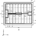
- FIG. 4A is an example of a top view of the semiconductor device 100 according to the embodiment.
- the semiconductor device 100 of this example differs from the semiconductor device 100 of FIG. 1A in that it includes a well region 115 provided symmetrically with respect to the central virtual line VL.
- the well region 115 is provided symmetrically with respect to the central virtual line VL in the stretching direction.
- the shortest distance R1 between the well region 115 and the trench center position TP can be made large.
- FIG. 4B is an example of a top view of the semiconductor device 100 according to the embodiment.
- the semiconductor device 100 of this example differs from the embodiment of FIG. 1A in the positional relationship between the position where the control pad is provided and the stretching direction of the trench portion.
- the first control pad 110 is provided so as to project from the first outer peripheral 151 extending in the X-axis direction to the inside of the semiconductor substrate 10.
- the second control pad 120 is provided so as to project from the second outer peripheral 152 extending in the X-axis direction to the inside of the semiconductor substrate 10.
- the plurality of trench portions are stretched in the stretching direction (Y-axis direction) in the top view. That is, the stretching direction of this example is orthogonal to the first outer peripheral 151 in the top view. Therefore, the plurality of trench portions have an extension direction in the same direction as the projecting direction (Y-axis direction) of the first control pad 110 and the second control pad 120. Also in this case, if the shortest distance R1a between the corner portion 111 and the trench center position TP satisfies the same conditions as in the other embodiments, the current concentration in the corner portion 111 can be avoided. Similarly, if the shortest distance R2a between the corner portion 121 and the trench center position TP satisfies the same conditions as in the other embodiments, current concentration in the corner portion 121 can be avoided.
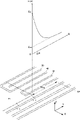
- FIG. 5 is a schematic diagram showing the electric field strength E (R) when the avalanche breakdown occurs in the vicinity of the corner portion 111 in the off state.
- E (R) indicates the electric field strength at a position R away from the corner portion 111.
- R is not limited to the direction shown in FIG. 5, and may be any direction in the top view plane (xy plane in the figure).
- R in this example indicates the distance from the corner portion 111 in the trench extending direction.
- the electric field strength E (R) converges to the maximum electric field strength Em calculated by the planar junction approximation regardless of the influence of the corner portion 111 in the well region.
- the electric field strength increases according to Poisson's formula represented by the formula (1) due to the influence of the corner portion 111 of the well region 115. ...
- q is the elementary charge
- ⁇ 0 is the permittivity of the vacuum
- ⁇ r is the relative permittivity
- p is the hole concentration
- ND is the donor concentration.
- the electron concentration and the acceptor concentration inside the depletion layer of the drift region 18 are sufficiently small and are ignored. That is, in the vicinity of the corner portion 111, the slope (divE) of the electric field strength E increases due to the curvature of the electric field in the xy plane of the upper surface. Therefore, the electric field strength E itself also increases. Therefore, E (R) increases from Em as it approaches the corner portion 111.
- E (R) the electric field strength E (R) follows the exponential function of R.
- E (R) Ep ⁇ exp ( ⁇ R / ⁇ R) + Em ⁇ ⁇ ⁇ Equation (2)
- Ep is the peak electric field strength at the corner 111
- ⁇ R is the characteristic length at which the electric field strength is attenuated.
- Ep may be the critical electric field strength as an example. In this example, Ep is 6E5 (V / cm).
- ⁇ R is, for example, about 200 ⁇ m to 400 ⁇ m. The ⁇ R of this example is 300 ⁇ m. However, ⁇ R is not limited to this range.
- E (R) is the value Em of the plane junction approximation.
- the average donor concentration of the drift layer is ND 0
- the applied voltage is V
- Em is expressed by the following equation from Poisson's equation.
- Em ⁇ 2V (q / ( ⁇ 0 ⁇ r ) (p + N D0 ) ⁇ 0.5 ... Equation (3)
- the hole concentration p for example, it is assumed that the transistor portion 70 is turned off, and here, it is assumed that a current of about the rated current Jrate is flowing.
- the velocity of the holes in the depletion layer (that is, the space charge region) may be saturated at vsat , and the hole concentration p satisfies the following equation (4).
- p Jrate / (qv sat ) ⁇ ⁇ ⁇ Equation (4)
- the v sat is, for example, 8 ⁇ 10 6 (cm / s) for holes in silicon.
- N D0 5E13 / cm 3
- applied voltage V 600V
- rated current density Jrate 500A / cm 2
- Em is 2.83E5 (V / cm).
- FIG. 6A is a diagram showing the distance R dependence of the electric field strength E (R) at a position separated from the corner portion 111 by a distance R.
- the vertical axis shows the ratio E (R) / Em normalized by the electric field strength E (R) (V / cm) and the maximum electric field strength Em, and the horizontal axis shows the distance R ( ⁇ m) from the corner portion 111.
- the electrolytic strength E (R) indicates an electric field strength of about the maximum electric field strength Em in the range where the distance R is 1500 ⁇ m or more.
- the electrolytic strength E (R) increases sharply as the distance R becomes shorter than 1500 ⁇ m.
- the ratio E (R) / Em of the electric field strength becomes 1.1 or more.
- Avalanche breakdown is a critical phenomenon, and the impact ionization coefficient strongly depends on the electric field strength. Therefore, when the electric field strength ratio E (R) / Em becomes 1.1 times or more, the impact ionization coefficient becomes 2 times or more, the impact ionization rate increases, and avalanche breakdown occurs strongly.
- the distance R may be replaced with the shortest distance R1a from the corner portion 111 to the trench center position TP. That is, the shortest distance R1a from the corner portion 111 to the trench center position TP may be 1000 ⁇ m or more, and may be 1500 ⁇ m or more. In this example, the distance R is replaced with the shortest distance R1a, but the shortest distance R1b, the shortest distance R2a, or the shortest distance R2b can also be replaced and described.
- the gate voltage When the gate voltage is turned off from + to-during turn-off, the potential is transmitted from the gate metal layer 50 to the gate conductive portion 44.
- the gate conductive portion 44 is made of polysilicon, the resistivity is higher than that of an aluminum alloy or the like.
- it is necessary to charge and discharge the MOS capacitor. A delay time occurs in the charging / discharging of the MOS capacitor due to the capacitance determined by the thickness of the gate insulating film 42 and the resistance of the gate conductive portion 44. The longer the length from the position of the gate metal layer 50 to the trench center position TP, the greater the resistance of the gate conductive portion 44.
- the delay time required for charging the MOS capacitor at the center position TP of the trench becomes long. Due to this increase in the delay time, it is delayed to turn off the gate near the trench center position TP, carriers are concentrated on the trench center position TP, and a current filament is generated. On the other hand, at the time of turn-off, the depletion layer spreads in the drift region 18, and the current filament exists in the depletion layer. Since a large amount of carriers (holes) remain in the current filament, the slope of the electric field strength of the depletion layer increases, and the electric field strength increases. In addition, the high current density (particularly hole current) also increases the impact ionization rate and enhances avalanche breakdown.
- the shortest distance R1a becomes shorter than 1000 ⁇ m.
- the electric field strength E (R1a) at the trench center position TP is higher than 1.1 times that of Em. Therefore, in the trench center position TP, the electric field strength increases not only with the current filament but also with the spatial distortion of the electric field. Then, the impact ionization rate increases not only in the vicinity of the corner portion 111 but also in the trench center position TP, and avalanche breakdown is likely to occur. As a result, the current causes positive feedback in the region including the corner portion 111 and the trench center position Tp, which increases the possibility of fracture.
- the shortest distance R1a may be 1500 ⁇ m or more.
- the shortest distance R1a is set to 1000 ⁇ m or more within the range of the above-mentioned conductive portion shape ratio ⁇ .
- the shortest distance R1a may be 1500 ⁇ m or more, 2000 ⁇ m or more, 3000 ⁇ m or more, and 5000 ⁇ m or more.
- the shortest distance R1a may be 20000 ⁇ m or less, 15000 ⁇ m or less, and 10000 ⁇ m or more.
- FIG. 6B is a graph showing the relationship between the shortest distance R1a and the defect rate (%) of the turn-off tolerance.
- the defect rate of the turn-off tolerance is the rate at which the semiconductor device is destroyed by the turn-off.
- the turn-off current density and applied voltage may vary and may be, for example, the conditions described above.
- the defect rate of the turn-off tolerance is shown when the conductive portion shape ratio ⁇ is 6250 and when the conductive portion shape ratio ⁇ is 8750.
- the defect rate of the turn-off tolerance is 50%. The defect rate is reduced to 14% when the shortest distance R1a is 1000 ⁇ m, 5% when the shortest distance R1a is 1500 ⁇ m, and 2% when the shortest distance R1a is 2000 ⁇ m.
- the shortest distance R1a When the conductive portion shape ratio ⁇ is 8750, the trench length Lt is 7000 ⁇ m, and the width Wg of the gate conductive portion 44 is 0.8 ⁇ m.
- the defect rate of the turn-off tolerance is 62%, and when the shortest distance R1a is 1000 ⁇ m, it decreases to 21%. Further, when the shortest distance R1a is 1500 ⁇ m or more, the defect rate is greatly reduced to 8% or less. Since the defect rate of the turn-off tolerance can be made lower than 30%, the shortest distance R1a may be 1000 ⁇ m or more, may be 1500 ⁇ m or more, 2000 ⁇ m or more, 3000 ⁇ m or more, and 5000 ⁇ m or more. May be. In this example, the shortest distance R1a has been described, but the shortest distance R1b, the shortest distance R2a, or the shortest distance R2b can also be described in the same manner.
- FIG. 6C is a graph showing the relationship between the rated voltage voltage and the rated current density J rate .
- the vertical axis shows the rated current density Jrate (A / cm 2 ), and the horizontal axis shows the rated voltage (V).
- the semiconductor device 100 may be designed to satisfy the rated voltage voltage and rated current density J rate in the region sandwiched between the upper limit P1 and the lower limit P2 in FIG. 6C.
- the semiconductor device 100 may be designed to satisfy a rated current density of 400 (A / cm 2 ) or more and 800 (A / cm 2 ) or less at a rated voltage of 600 (V). Further, the semiconductor device 100 may be designed so as to satisfy a rated current density of 300 (A / cm 2 ) or more and 600 (A / cm 2 ) or less at a rated voltage of 1200 (V). The semiconductor device 100 may be designed to satisfy a rated current density of 200 (A / cm 2 ) or more and 400 (A / cm 2 ) or less at a rated voltage of 1700 (V).
- the distance between the P-shaped well region and the trench center position TP is appropriately set. By setting it, it is possible to avoid element destruction due to the inflow of the current filament into the P-shaped well region.
- contact hole 56. ⁇ ⁇ Contact hole, 70 ⁇ ⁇ ⁇ Transistor part, 71 ⁇ ⁇ ⁇ Mesa part, 80 ⁇ ⁇ ⁇ Diode part, 81 ⁇ ⁇ ⁇ Mesa part, 82 ⁇ ⁇ ⁇ Cathode region, 90 ⁇ ⁇ ⁇ Boundary part, 91 ⁇ ⁇ Mesa part, 92 ... boundary part, 100 ... semiconductor device, 102 ... active part, 104 ... outer peripheral part, 110 ... first control pad, 111 ... corner part, 112. Anode pad, 114 ... cathode pad, 115 ... well area, 116 ... sense pad, 118 ... notch, 120 ... second control pad, 121 ...
Landscapes
- Metal-Oxide And Bipolar Metal-Oxide Semiconductor Integrated Circuits (AREA)
Abstract
半導体基板(10)に設けられた活性部(102)と、ゲート導電部(44)を有し、活性部において、予め定められた延伸方向に延伸して設けられ、予め定められた配列方向に配列された複数のトレンチ部(40)であって、延伸方向におけるトレンチ長さ(Lt)に対する、ゲート導電部の配列方向における幅(Wg)の導電部形状比が1000以上である複数のトレンチ部と、上面視において、半導体基板の予め定められた第1外周辺(151)から半導体基板の内側に張り出して設けられた第1制御パッド(110)と、第1制御パッドの下方に設けられ、上面視において第1制御パッドを覆って設けられた第1ウェル領域(115)とを備え、上面視において、第1ウェル領域と、複数のトレンチ部の延伸方向における長さの中央であるトレンチ中央位置(TP)との間の最短距離(R1a)が1000μm以上である半導体装置(100)を提供する。
Description
本発明は、半導体装置に関する。
従来、複数のトレンチ部を備える半導体装置であって、制御パッドの下方にウェル領域を設けた半導体装置が知られている。
[先行技術文献]
[特許文献]
[特許文献1]国際公開第2019/078166号
[特許文献2]特開2020-077674号公報
[特許文献3]特開2019-186510号公報
[特許文献4]国際公開第2018/154963号
[先行技術文献]
[特許文献]
[特許文献1]国際公開第2019/078166号
[特許文献2]特開2020-077674号公報
[特許文献3]特開2019-186510号公報
[特許文献4]国際公開第2018/154963号
半導体装置の破壊を回避することが好ましい。
本発明の第1の態様においては、半導体基板に設けられた活性部と、ゲート導電部を有し、活性部において、予め定められた延伸方向に延伸して設けられ、予め定められた配列方向に配列された複数のトレンチ部であって、延伸方向におけるトレンチ長さに対する、ゲート導電部の配列方向における幅の導電部形状比が1000以上である複数のトレンチ部と、上面視において、半導体基板の予め定められた第1外周辺から半導体基板の内側に張り出して設けられた第1制御パッドと、第1制御パッドの下方に設けられ、上面視において第1制御パッドを覆って設けられた第1ウェル領域とを備え、上面視において、第1ウェル領域と、複数のトレンチ部の延伸方向における長さの中央であるトレンチ中央位置との間の最短距離が1000μm以上である半導体装置を提供する。
最短距離は、1500μm以上であってよい。
最短距離は、2000μm以上であってよい。
複数のトレンチ部の導電部形状比は、3000以上、1×10⁶以下であってよい。
複数のトレンチ部は、ゲート電位に設定されたゲートトレンチ部を含んでよい。ゲートトレンチ部の導電部形状比は、5000以上、3×10⁵以下であってよい。
第1制御パッドは、アノードパッド、カソードパッドおよびセンスパッドを含んでよい。
第1ウェル領域は、上面視で矩形を有し、第1ウェル領域の3辺が活性部と対向して設けられてよい。
第1ウェル領域は、第1外周辺から張り出して設けられた角部を有してよい。最短距離は、第1ウェル領域の角部と、トレンチ中央位置との距離であってよい。
第1外周辺と直交し、第1外周辺の中央を通る中央仮想線から、第1ウェル領域の角部までの距離L1aは、中央仮想線と直交する方向における中央仮想線から半導体基板の外周端までの長さの40%以上であってよい。
第1ウェル領域は、第1外周辺と直交して第1外周辺の中央を通る中央仮想線に対して対称に設けられてよい。
第1ウェル領域は、第1外周辺と直交して第1外周辺の中央を通る中央仮想線に対して非対称に設けられてよい。
第1ウェル領域は、上面視において、角の一部が切り取られた切欠部を備えてよい。
上面視において、第1外周辺と対向する第2外周辺から半導体基板の内側に張り出して設けられた第2制御パッドと、第2制御パッドの下方に設けられ、上面視において第2制御パッドを覆って設けられた第2ウェル領域とを備えてよい。第2ウェル領域は、第2外周辺から張り出して設けられた角部を有してよい。距離L1aは、延伸方向における中央仮想線から第2ウェル領域の角部までの距離L2aより長くてよい。
第2制御パッドは、複数のトレンチ部をゲート電位に設定するためのゲートパッドを含んでよい。
活性部は、トランジスタ部およびダイオード部を備えてよい。第1ウェル領域の角部は、上面視において、トランジスタ部に位置してよい。
複数のトレンチ部がエミッタ電位に設定されたダミートレンチ領域を備えてよい。第1ウェル領域の角部は、上面視において、ダミートレンチ領域に位置してよい。
活性部は、トランジスタ部およびダイオード部を備えてよい。第1ウェル領域の角部は、上面視において、ダイオード部に位置してよい。
半導体装置は、半導体基板の上方に設けられた保護膜を備えてよい。ダイオード部は、半導体基板のおもて面側にライフタイム制御領域を有してよい。保護膜は、上面視において、ダイオード部を避けて設けられてよい。
延伸方向は、上面視において、第1外周辺と平行であってよい。
延伸方向は、上面視において、第1外周辺と直交してよい。
なお、上記の発明の概要は、本発明の必要な特徴の全てを列挙したものではない。また、これらの特徴群のサブコンビネーションもまた、発明となりうる。
以下、発明の実施の形態を通じて本発明を説明するが、以下の実施形態は請求の範囲にかかる発明を限定するものではない。また、実施形態の中で説明されている特徴の組み合わせの全てが発明の解決手段に必須であるとは限らない。
本明細書においては半導体基板の深さ方向と平行な方向における一方の側を「上」、他方の側を「下」と称する。基板、層またはその他の部材の2つの主面のうち、一方の面を上面、他方の面を下面と称する。「上」、「下」の方向は、重力方向または半導体装置の実装時における方向に限定されない。
本明細書では、X軸、Y軸およびZ軸の直交座標軸を用いて技術的事項を説明する場合がある。直交座標軸は、構成要素の相対位置を特定するに過ぎず、特定の方向を限定するものではない。例えば、Z軸は地面に対する高さ方向を限定して示すものではない。なお、+Z軸方向と-Z軸方向とは互いに逆向きの方向である。正負を記載せず、Z軸方向と記載した場合、+Z軸および-Z軸に平行な方向を意味する。
本明細書では、半導体基板の上面および下面に平行な直交軸をX軸およびY軸とする。また、半導体基板の上面および下面と垂直な軸をZ軸とする。本明細書では、Z軸の方向を深さ方向と称する場合がある。また、本明細書では、X軸およびY軸を含めて、半導体基板の上面および下面に平行な方向を、水平方向と称する場合がある。
本明細書において「同一」または「等しい」のように称した場合、製造ばらつき等に起因する誤差を有する場合も含んでよい。当該誤差は、例えば10%以内である。
本明細書においては、不純物がドーピングされたドーピング領域の導電型をP型またはN型として説明している。本明細書においては、不純物とは、特にN型のドナーまたはP型のアクセプタのいずれかを意味する場合があり、ドーパントと記載する場合がある。本明細書においては、ドーピングとは、半導体基板にドナーまたはアクセプタを導入し、N型の導電型を示す半導体またはP型の導電型を示す半導体とすることを意味する。
本明細書においては、ドーピング濃度とは、熱平衡状態におけるドナーの濃度またはアクセプタの濃度を意味する。本明細書においては、ネット・ドーピング濃度とは、ドナー濃度を正イオンの濃度とし、アクセプタ濃度を負イオンの濃度として、電荷の極性を含めて足し合わせた正味の濃度を意味する。一例として、ドナー濃度をND、アクセプタ濃度をNAとすると、任意の位置における正味のネット・ドーピング濃度はND-NAとなる。本明細書では、ネット・ドーピング濃度を単にドーピング濃度と記載する場合がある。
ドナーは、半導体に電子を供給する機能を有している。アクセプタは、半導体から電子を受け取る機能を有している。ドナーおよびアクセプタは、不純物自体には限定されない。例えば、半導体中に存在する空孔(V)、酸素(O)および水素(H)が結合したVOH欠陥は、電子を供給するドナーとして機能する。本明細書では、VOH欠陥を水素ドナーと称する場合がある。
本明細書においてP+型またはN+型と記載した場合、P型またはN型よりもドーピング濃度が高いことを意味し、P-型またはN-型と記載した場合、P型またはN型よりもドーピング濃度が低いことを意味する。また、本明細書においてP++型またはN++型と記載した場合には、P+型またはN+型よりもドーピング濃度が高いことを意味する。本明細書の単位系は、特に断りがなければSI単位系である。長さの単位をcmあるいはμmで表示することがあるが、諸計算はメートル(m)に換算してから行ってよい。
図1Aは、実施例に係る半導体装置100の上面図の一例を示す。半導体装置100は、トランジスタ部70およびダイオード部80を備える半導体チップである。半導体装置100は、IPM(Intelligent Power Module)等のモジュールに搭載されてよい。
トランジスタ部70は、半導体装置100においてトランジスタ動作をする領域である。トランジスタ部70は、IGBT(Insulated Gate Bipolar Transistor)等のトランジスタを含む。ダイオード部80は、半導体装置100において、回路の電流を還流させる等のダイオード動作をする領域である。ダイオード部80は、還流ダイオード(FWD:Free Wheel Diode)等のダイオードを含む。本例の半導体装置100は、トランジスタ部70およびダイオード部80を同一のチップに有する逆導通IGBT(RC-IGBT:Reverse Conducting IGBT)である。なお、各図面において、トランジスタ部70の領域を記号I、ダイオード部80の領域を記号Fで示す場合がある。
半導体基板10は、シリコン基板であってよく、炭化シリコン基板であってよく、窒化ガリウム等の窒化物半導体基板等であってもよい。本例の半導体基板10は、シリコン基板である。半導体基板10は、活性部102および外周部104を有する。本明細書では、上面視における半導体基板10の外周の端部を、外周端150とする。上面視とは、半導体基板10のおもて面側から、当該おもて面と垂直な方向(Z軸方向)に見た場合を指す。
トランジスタ部70およびダイオード部80は、XY平面内において交互に周期的に配列されてよい。トランジスタ部70およびダイオード部80の間の領域において、半導体基板10の上方には、ゲート金属層50が設けられてよい。なお、本例のトランジスタ部70およびダイオード部80は、Y軸方向に延伸して、X軸方向に配列されたトレンチ部を有する。但し、トランジスタ部70およびダイオード部80は、X軸方向に延伸して、Y軸方向に配列されたトレンチ部を有していてもよい。なお、トランジスタ部70またはダイオード部80に隣接する領域には、後述する境界部90および境界部92が設けられてよい。境界部92は、活性部102のうち、上面視においてダイオード部80とゲート金属層50との間の領域であってよい。本例の境界部92は、Y軸方向において、ダイオード部80とゲート金属層50との間の領域に設けられており、X軸方向において、トランジスタ部70の間に設けられている。境界部92においては、半導体基板10の裏面に後述するコレクタ領域22が設けられてよい。
活性部102は、トランジスタ部70およびダイオード部80を有する。活性部102は、半導体装置100をオン状態に制御した場合に、半導体基板10のおもて面と裏面との間で主電流が流れる領域である。即ち、半導体基板10のおもて面から裏面、または裏面からおもて面に、半導体基板10の内部を深さ方向に電流が流れる領域である。本明細書では、トランジスタ部70およびダイオード部80をそれぞれ素子部または素子領域と称する。
なお、上面視において、2つの素子部に挟まれた領域も活性部102とする。本例では、素子部に挟まれてゲート金属層50が設けられている領域も活性部102に含めている。
ゲート金属層50は、金属を含む材料で形成される。例えば、ゲート金属層50は、アルミニウム、アルミニウム‐シリコン合金、またはアルミニウム‐シリコン-銅合金で形成される。ゲート金属層50は、トランジスタ部70のゲート導電部と電気的に接続され、トランジスタ部70にゲート電圧を供給する。ゲート金属層50は、上面視で、活性部102の外周を囲うように設けられる。ゲート金属層50は、外周部104に設けられるゲートパッド122と電気的に接続される。ゲート金属層50は、半導体基板10の外周端150に沿って設けられてよい。また、ゲート金属層50は、上面視で、温度センス部140の周囲や、トランジスタ部70およびダイオード部80の間に設けられてよい。本例のゲート金属層50は、太線で示されている。
外周部104は、上面視において、活性部102と半導体基板10の外周端150との間の領域である。外周部104は、上面視において、活性部102を囲んで設けられる。外周部104には、半導体装置100と外部の装置とをワイヤ等で接続するための1つ以上の金属のパッドが配置されてよい。なお、外周部104は、エッジ終端構造部を有してよい。エッジ終端構造部は、半導体基板10のおもて面側の電界集中を緩和する。例えば、エッジ終端構造部は、ガードリング、フィールドプレート、リサーフおよびこれらを組み合わせた構造を有する。
おもて面電極は、半導体基板10の上方に設けられる。おもて面電極は、後述するエミッタ電極52を含む。おもて面電極は、第1制御パッド110および第2制御パッド120を含んでよい。おもて面電極は、ワイヤボンディング等によって、半導体装置100の外部の電極と接続されてよい。なお、おもて面電極の個数および位置は、本例に限定されない。
第1制御パッド110は、上面視において、半導体基板10の予め定められた第1外周辺151から半導体基板10の内側に張り出して設けられている。第1制御パッド110が第1外周辺151から半導体基板10の内側に張り出すとは、活性部102の内側に外周部104が延伸して設けられていることを指す。即ち、第1制御パッド110のY軸方向の正側または負側には、活性部102が設けられている。本例の第1制御パッド110は、アノードパッド112と、カソードパッド114と、センスパッド116とを備える。
第2制御パッド120は、上面視において、第2外周辺152から半導体基板10の内側に張り出して設けられている。第2外周辺152は、第1外周辺151と対向する外周端150の辺である。なお、本例の第1外周辺151および第2外周辺152は、上面視において、トレンチ部の延伸方向(本例ではY軸方向)と平行である。本例の第2制御パッド120は、ゲートパッド122を備える。
ウェル領域115は、第1制御パッド110の下方に設けられ、上面視において第1制御パッド110を覆って設けられている。本例のウェル領域115は、上面視で矩形を有し、ウェル領域115の3辺が活性部102と対向して設けられている。ウェル領域115は、第1外周辺151から張り出して設けられた角部111を有する。
ウェル領域125は、第2制御パッド120の下方に設けられ、上面視において第2制御パッド120を覆って設けられている。本例のウェル領域125は、上面視で矩形を有し、ウェル領域125の3辺が活性部102と対向して設けられている。ウェル領域125は、第2外周辺152から張り出して設けられた角部121を有する。
ウェル領域135は、上面視においてゲート金属層50を覆うように設けられている。本例のウェル領域135は、外周部104に沿って、ゲート金属層50を覆って設けられている。ウェル領域135は、ウェル領域115と接続されてよい。
ウェル領域145は、上面視においてゲート金属層50を覆うように設けられている。本例のウェル領域145は、温度センス部140および温度センス配線142をさらに覆って設けられてよい。ウェル領域145は、ウェル領域115およびウェル領域125に接続されてよい。
ウェル領域115、ウェル領域125、ウェル領域135およびウェル領域145は、半導体基板10のおもて面側に設けられた第2導電型の領域である。ウェル領域115、ウェル領域125、ウェル領域135およびウェル領域145の導電型は、一例としてP+型である。ウェル領域115、ウェル領域125、ウェル領域135およびウェル領域145を設けることにより、半導体基板10内のホールを引き抜きやすくなり、ラッチアップしにくくなる。これにより半導体装置100の耐量を向上することができる。
ゲートパッド122は、ゲート金属層50と電気的に接続される。ゲートパッド122は、ゲート金属層50を介してトランジスタ部70のゲート導電部と電気的に接続される。ゲートパッド122は、ゲート電位に設定されている。本例のゲートパッド122は、上面視で矩形である。一例において、ゲートパッド122は、1000μm以上、1500μm以下の1辺を有してよいが、これに限定されない。
アノードパッド112は、温度センス部140のアノード領域と電気的に接続される。アノードパッド112は、温度センス配線142によって、温度センス部140のアノード領域と電気的に接続されている。本例のアノードパッド112は、上面視で矩形である。一例において、アノードパッド112は、500μm以上、900μm以下の短辺と、1000μm以上、1500μm以下の長辺とを有してよいが、これに限定されない。
カソードパッド114は、温度センス部140のカソード領域と電気的に接続される。カソードパッド114は、温度センス配線142によって、温度センス部140のカソード領域と電気的に接続されている。本例のカソードパッド114は、上面視で矩形である。カソードパッド114は、上面視において、アノードパッド112と同一の形状を有してもよい。
温度センス部140は、活性部102の上方に配置され、半導体基板10の温度を検出する。本例の温度センス部140は、活性部102の温度を検知する。温度センス部140は、ポリシリコン等の半導体材料で形成されるダイオードを有してよい。温度センス部140は、半導体装置100の温度を検出して、半導体チップを過熱から保護するために用いられる。温度センス部140は、X軸方向に長手を有し、Y軸方向に短手を有するが、これに限られない。
本例の温度センス部140は、上面視で、活性部102の中央付近に設けられる。温度センス部140は、トランジスタ部70およびダイオード部80のいずれの領域に設けられてもよい。即ち、温度センス部140が設けられた半導体基板10の裏面側には、第2導電型のコレクタ領域が設けられても第1導電型のカソード領域が設けられてもよい。
温度センス配線142は、アノードパッド112およびカソードパッド114を温度センス部140と電気的に接続する。温度センス配線142は、活性部102の上方において、温度センス部140から外周部104まで延伸して設けられる。温度センス配線142は、おもて面電極と同一の材料で構成されてもよい。上面視において、温度センス部140および温度センス配線142と重なる半導体基板10の領域には、P+型のウェル領域が配置されてよい。
図1Bは、半導体装置100の上面の拡大図を示す。本例では、図1Aの領域Aの拡大図が示されている。
トランジスタ部70は、半導体基板10の裏面側に設けられたコレクタ領域22を半導体基板10のおもて面に投影した領域であってよい。コレクタ領域22は、第2導電型を有する。本例のコレクタ領域22は、一例としてP+型である。トランジスタ部70は、トランジスタ部70とダイオード部80の境界に位置する境界部90を含む。
ダイオード部80は、半導体基板10の裏面側に設けられたカソード領域82を半導体基板10のおもて面に投影した領域であってよい。カソード領域82は、第1導電型を有する。本例のカソード領域82は、一例としてN+型である。
本例の半導体装置100は、半導体基板10のおもて面において、ゲートトレンチ部40と、ダミートレンチ部30と、エミッタ領域12と、ベース領域14と、コンタクト領域15と、ウェル領域145とを備える。また、本例の半導体装置100は、半導体基板10のおもて面の上方に設けられたエミッタ電極52およびゲート金属層50を備える。
エミッタ電極52は、ゲートトレンチ部40、ダミートレンチ部30、エミッタ領域12、ベース領域14、コンタクト領域15およびウェル領域145の上方に設けられている。また、ゲート金属層50は、ゲートトレンチ部40およびウェル領域145の上方に設けられている。
エミッタ電極52およびゲート金属層50は、金属を含む材料で形成される。例えば、エミッタ電極52の少なくとも一部の領域は、アルミニウム、アルミニウム‐シリコン合金、またはアルミニウム‐シリコン-銅合金で形成されてよい。エミッタ電極52は、アルミニウム等で形成された領域の下層にチタンやチタン化合物等で形成されたバリアメタルを有してよい。エミッタ電極52およびゲート金属層50は、互いに分離して設けられる。
エミッタ電極52およびゲート金属層50は、層間絶縁膜38を挟んで、半導体基板10の上方に設けられる。層間絶縁膜38は、図1Aでは省略されている。層間絶縁膜38には、コンタクトホール54、コンタクトホール55およびコンタクトホール56が貫通して設けられている。
コンタクトホール55は、ゲート金属層50とトランジスタ部70内のゲート導電部とを接続する。コンタクトホール55の内部には、タングステン等で形成されたプラグが形成されてもよい。コンタクトホール56は、エミッタ電極52とダミートレンチ部30内のダミー導電部とを接続する。コンタクトホール56の内部には、タングステン等で形成されたプラグが形成されてもよい。
接続部25は、エミッタ電極52またはゲート金属層50等のおもて面電極と、トレンチ部の内部に形成された導電部とを電気的に接続する。一例において、接続部25は、ゲート金属層50とゲート導電部との間に設けられる。接続部25は、エミッタ電極52とダミー導電部との間にも設けられている。接続部25は、不純物がドープされたポリシリコン等の導電性の材料を含む。本例の接続部25は、N型の不純物がドープされたポリシリコン(N+)である。接続部25は、酸化膜等の絶縁膜等を介して、半導体基板10のおもて面の上方に設けられる。
ゲートトレンチ部40は、所定の配列方向(本例ではX軸方向)に沿って所定の間隔で配列される。本例のゲートトレンチ部40は、半導体基板10のおもて面に平行であって配列方向と垂直な延伸方向(本例ではY軸方向)に沿って延伸する2つの延伸部分41と、2つの延伸部分41を接続する接続部分43を有してよい。ゲートトレンチ部40は、ゲート電位に設定されている。
接続部分43は、少なくとも一部が曲線状に形成されることが好ましい。ゲートトレンチ部40の2つの延伸部分41の端部を接続することで、延伸部分41の端部における電界集中を緩和できる。ゲートトレンチ部40の接続部分43において、ゲート金属層50がゲート導電部と接続されてよい。
ダミートレンチ部30は、エミッタ電極52と電気的に接続されたトレンチ部である。ダミートレンチ部30は、ゲートトレンチ部40と同様に、所定の配列方向(本例ではX軸方向)に沿って所定の間隔で配列される。本例のダミートレンチ部30は、ゲートトレンチ部40と同様に、半導体基板10のおもて面においてU字形状を有してよい。即ち、ダミートレンチ部30は、延伸方向に沿って延伸する2つの延伸部分31と、2つの延伸部分31を接続する接続部分33を有してよい。
本例のトランジスタ部70は、2つのゲートトレンチ部40と3つのダミートレンチ部30を繰り返し配列させた構造を有する。即ち、本例のトランジスタ部70は、2:3の比率でゲートトレンチ部40とダミートレンチ部30を有している。例えば、トランジスタ部70は、2本の延伸部分41の間に1本の延伸部分31を有する。また、トランジスタ部70は、ゲートトレンチ部40と隣接して、2本の延伸部分31を有している。
但し、ゲートトレンチ部40とダミートレンチ部30の比率は本例に限定されない。ゲートトレンチ部40とダミートレンチ部30の比率は、1:1であってもよく、2:4であってもよい。また、トランジスタ部70においてダミートレンチ部30を設けず、全てゲートトレンチ部40としたいわゆるフルゲートトレンチ構造(オールゲートトレンチ構造)としてもよい。
ウェル領域145は、後述するドリフト領域18よりも半導体基板10のおもて面側に設けられた第2導電型の領域である。ウェル領域145は、半導体装置100のエッジ側に設けられるウェル領域の一例である。ウェル領域145は、一例としてP+型である。ウェル領域145は、ゲート金属層50が設けられる側の活性領域の端部から、予め定められた範囲で形成される。ウェル領域145の拡散深さは、ゲートトレンチ部40およびダミートレンチ部30の深さよりも深くてよい。ゲートトレンチ部40およびダミートレンチ部30の、ゲート金属層50側の一部の領域は、ウェル領域145に形成される。ゲートトレンチ部40およびダミートレンチ部30の延伸方向の端の底は、ウェル領域145に覆われてよい。ウェル領域145は、ウェル領域115およびウェル領域125と同時に形成されてよい。ウェル領域115、ウェル領域125、ウェル領域135およびウェル領域145の拡散深さは同じ、または実質的に同じであってよい。ウェル領域145は、上面視でゲート金属層50を覆うように設けられてよい。ウェル領域145は、トランジスタ部70またはダイオード部80よりも外周側の、外周部104に近い位置でエミッタ電極52と電気的に接続してよい。
コンタクトホール54は、層間絶縁膜38を開口して半導体基板10のおもて面21を露出した部分である。コンタクトホール54は、トランジスタ部70において、エミッタ領域12およびコンタクト領域15の各領域の上方に形成される。コンタクトホール54を介して、エミッタ領域12またはコンタクト領域15はエミッタ電極52と接触し、電気的に接続する。
ダイオード部80において、コンタクトホール54はベース領域14の上方に設けられる。ダイオード部80におけるベース領域14は、コンタクトホール54を介してエミッタ電極52と接してよい。コンタクトホール54が形成されたおもて面21において、ベース領域14とエミッタ電極52との間に、コンタクト抵抗を低減するために、ベース領域14と同じ導電型の高濃度層を備えてもよい。
境界部90において、コンタクトホール54はコンタクト領域15の上方に設けられる。コンタクトホール54は、Y軸方向両端に設けられたウェル領域145の上方には設けられていなくてよい。このように、層間絶縁膜38には、1又は複数のコンタクトホール54が形成されている。1又は複数のコンタクトホール54は、延伸方向に延伸して設けられてよい。
境界部90は、トランジスタ部70に設けられ、ダイオード部80と隣接する領域である。境界部90は、コンタクト領域15を有してよい。本例の境界部90は、エミッタ領域12を有さない。一例において、境界部90のトレンチ部は、ダミートレンチ部30である。本例の境界部90は、X軸方向における両端がダミートレンチ部30となるように配置されている。
メサ部71、メサ部91およびメサ部81は、半導体基板10のおもて面と平行な面内において、トレンチ部に隣接して設けられたメサ部である。メサ部とは、隣り合う2つのトレンチ部に挟まれた半導体基板10の部分であって、半導体基板10のおもて面から、各トレンチ部の最も深い底部の深さまでの部分であってよい。各トレンチ部の延伸部分を1つのトレンチ部としてよい。即ち、2つの延伸部分に挟まれる領域をメサ部としてよい。
メサ部71は、トランジスタ部70において、ダミートレンチ部30またはゲートトレンチ部40の少なくとも1つに隣接して設けられる。メサ部71は、半導体基板10のおもて面において、エミッタ領域12と、ベース領域14と、コンタクト領域15と、ウェル領域145とを有してよい。メサ部71では、エミッタ領域12およびコンタクト領域15が延伸方向において交互に設けられてよい。
メサ部91は、境界部90に設けられている。メサ部91は、半導体基板10のおもて面において、コンタクト領域15またはウェル領域145を有してよい。
メサ部81は、ダイオード部80において、隣り合うダミートレンチ部30に挟まれた領域に設けられる。メサ部81は、半導体基板10のおもて面において、ベース領域14と、コンタクト領域15または、ウェル領域145を有してよい。
ベース領域14は、トランジスタ部70およびダイオード部80において、半導体基板10のおもて面側に設けられた第2導電型の領域である。ベース領域14は、一例としてP-型である。ベース領域14は、半導体基板10のおもて面において、メサ部71およびメサ部91のY軸方向における両端部に設けられてよい。なお、図1Aは、当該ベース領域14のY軸方向の一方の端部のみを示している。ベース領域14は、ウェル領域145よりもドーピング濃度が低くてよい。
エミッタ領域12は、ドリフト領域18よりもドーピング濃度の高い第1導電型の領域である。本例のエミッタ領域12は、一例としてN+型である。エミッタ領域12のドーパントの一例はヒ素(As)である。エミッタ領域12は、メサ部71のおもて面において、ゲートトレンチ部40と接して設けられる。エミッタ領域12は、メサ部71を挟んだ2本のトレンチ部の一方から他方まで、X軸方向に延伸して設けられてよい。エミッタ領域12は、コンタクトホール54の下方にも設けられている。
また、エミッタ領域12は、ダミートレンチ部30と接してもよいし、接しなくてもよい。本例のエミッタ領域12は、ダミートレンチ部30と接している。エミッタ領域12は、境界部90のメサ部91には設けられなくてよい。
コンタクト領域15は、ベース領域14よりもドーピング濃度の高い第2導電型の領域である。本例のコンタクト領域15は、一例としてP+型である。コンタクト領域15の深さ方向の厚さは、ベース領域14の深さ方向の厚さよりも薄くてよい。本例のコンタクト領域15は、メサ部71およびメサ部91のおもて面に設けられている。コンタクト領域15は、メサ部71またはメサ部91を挟んだ2本のトレンチ部の一方から他方まで、X軸方向に設けられてよい。コンタクト領域15は、ゲートトレンチ部40と接してもよいし、接しなくてもよい。また、コンタクト領域15は、ダミートレンチ部30と接してもよいし、接しなくてもよい。本例においては、コンタクト領域15が、ダミートレンチ部30およびゲートトレンチ部40と接する。コンタクト領域15は、コンタクトホール54の下方にも設けられている。なお、コンタクト領域15は、メサ部81にも設けられてよい。
トレンチ長さLtは、複数のトレンチ部の延伸方向における長さである。本例のトレンチ長さLtは、トレンチ部のY軸方向の正側に設けられたゲート金属層50と、トレンチ部のY軸方向の負側に設けられたゲート金属層50との間の距離に対応する。トレンチ長さLtは、2000μm以上であってよく、3000μm以上であってよく、4000μm以上であってよく、4600μm以上であってよく、6000μm以上であってよい。また、トレンチ長さLtは、50000μm以下であってよく、30000μm以下であってよく、20000μm以下であってよい。
図1Cは、図1Bにおけるa-a'断面の一例を示す図である。a-a'断面は、トランジスタ部70において、エミッタ領域12を通過するXZ面である。本例の半導体装置100は、a-a'断面において、半導体基板10、層間絶縁膜38、エミッタ電極52およびコレクタ電極24を有する。エミッタ電極52は、半導体基板10および層間絶縁膜38の上方に形成される。
ドリフト領域18は、半導体基板10に設けられた第1導電型の領域である。本例のドリフト領域18は、一例としてN-型である。ドリフト領域18は、半導体基板10において他のドーピング領域が形成されずに残存した領域であってよい。即ち、ドリフト領域18のドーピング濃度は半導体基板10のドーピング濃度であってよい。
バッファ領域20は、ドリフト領域18の下方に設けられた第1導電型の領域である。本例のバッファ領域20は、一例としてN型である。バッファ領域20のドーピング濃度は、ドリフト領域18のドーピング濃度よりも高い。バッファ領域20は、ベース領域14の裏面側から広がる空乏層が、第2導電型のコレクタ領域22および第1導電型のカソード領域82に到達することを防ぐフィールドストップ層として機能してよい。
コレクタ領域22は、トランジスタ部70において、バッファ領域20の下方に設けられる。カソード領域82は、ダイオード部80において、バッファ領域20の下方に設けられる。コレクタ領域22とカソード領域82との境界は、トランジスタ部70とダイオード部80との境界としてよい。
コレクタ電極24は、半導体基板10の裏面23に形成される。コレクタ電極24は、金属等の導電材料で形成される。
ベース領域14は、メサ部71、メサ部91およびメサ部81において、ドリフト領域18の上方に設けられる第2導電型の領域である。ベース領域14は、ゲートトレンチ部40に接して設けられてよい。ベース領域14は、ダミートレンチ部30に接して設けられてよい。
エミッタ領域12は、メサ部71において、ベース領域14とおもて面21との間に設けられる。エミッタ領域12は、ゲートトレンチ部40と接して設けられてよい。エミッタ領域12は、ダミートレンチ部30と接してもよいし、接しなくてもよい。なお、エミッタ領域12は、メサ部91に設けられなくてよい。
コンタクト領域15は、メサ部91において、ベース領域14の上方に設けられる。コンタクト領域15は、メサ部91において、ゲートトレンチ部40に接して設けられる。他の断面において、コンタクト領域15は、メサ部71のおもて面21に設けられてよい。
蓄積領域16は、ドリフト領域18よりも半導体基板10のおもて面21側に設けられる第1導電型の領域である。本例の蓄積領域16は、一例としてN+型である。蓄積領域16のドナー濃度は、ドリフト領域18のドナー濃度よりも大きい。蓄積領域16は、トランジスタ部70およびダイオード部80に設けられる。本例の蓄積領域16は、境界部90にも設けられている。これにより、半導体装置100は、蓄積領域16のマスクずれを回避できる。
また、蓄積領域16は、ゲートトレンチ部40に接して設けられる。蓄積領域16は、ダミートレンチ部30に接してもよいし、接しなくてもよい。蓄積領域16のドーピング濃度は、ドリフト領域18のドーピング濃度よりも高い。蓄積領域16を設けることで、キャリア注入促進効果(IE効果)を高めて、トランジスタ部70のオン電圧を低減できる。
1つ以上のゲートトレンチ部40および1つ以上のダミートレンチ部30は、おもて面21に設けられる。各トレンチ部は、おもて面21からドリフト領域18まで設けられる。エミッタ領域12、ベース領域14、コンタクト領域15および蓄積領域16の少なくともいずれかが設けられる領域においては、各トレンチ部はこれらの領域も貫通して、ドリフト領域18に到達する。トレンチ部がドーピング領域を貫通するとは、ドーピング領域を形成してからトレンチ部を形成する順序で製造したものに限定されない。トレンチ部を形成した後に、トレンチ部の間にドーピング領域を形成したものも、トレンチ部がドーピング領域を貫通しているものに含まれる。
ゲートトレンチ部40は、おもて面21に形成されたゲートトレンチ、ゲート絶縁膜42およびゲート導電部44を有する。ゲート絶縁膜42は、ゲートトレンチの内壁を覆って形成される。ゲート絶縁膜42は、ゲートトレンチの内壁の半導体を酸化または窒化して形成してよい。ゲート導電部44は、ゲートトレンチの内部においてゲート絶縁膜42よりも内側に形成される。ゲート絶縁膜42は、ゲート導電部44と半導体基板10とを絶縁する。ゲート導電部44は、ポリシリコン等の導電材料で形成される。ゲートトレンチ部40は、おもて面21において層間絶縁膜38により覆われる。
ゲート導電部44は、半導体基板10の深さ方向において、ゲート絶縁膜42を挟んでメサ部71側で隣接するベース領域14と対向する領域を含む。ゲート導電部44に所定の電圧が印加されると、ベース領域14のうちゲートトレンチに接する界面の表層に、電子の反転層によるチャネルが形成される。
ゲートトレンチ部40の幅は、0.5μmより大きくてよく、2.0μmより小さくてよい。本例のゲートトレンチ部40の幅は、1.0μmである。ゲート絶縁膜42の厚さは、0.05μmより厚くてよく、0.2μmより薄くてよい。本例のゲート絶縁膜42の厚さは、0.1μmである。
ゲート導電部44の幅Wgは、ゲートトレンチ部40の幅からゲート絶縁膜42の厚さ(即ち、ゲート絶縁膜42の二層分)を引けばよい。ゲートトレンチ部40の幅は、深さ方向に一定であってよく、増加してよく、減少してよい。ゲート導電部44の幅Wgは、ベース領域14においてドーピング濃度がピークとなる深さと同じ深さ位置における、ゲート導電部44の幅としてよい。または、ゲート導電部44の幅Wgは、ベース領域14がエミッタ領域12と接する深さ、即ちpn接合深さにおけるゲート導電部44の幅としてよい。
ダミートレンチ部30は、ゲートトレンチ部40と同一の構造を有してよい。ダミートレンチ部30は、おもて面21側に形成されたダミートレンチ、ダミー絶縁膜32およびダミー導電部34を有する。ダミー絶縁膜32は、ダミートレンチの内壁を覆って形成される。ダミー導電部34は、ダミートレンチの内部に形成され、且つ、ダミー絶縁膜32よりも内側に形成される。ダミー絶縁膜32は、ダミー導電部34と半導体基板10とを絶縁する。ダミートレンチ部30は、おもて面21において層間絶縁膜38により覆われる。
層間絶縁膜38は、おもて面21に設けられている。層間絶縁膜38の上方には、エミッタ電極52が設けられている。層間絶縁膜38には、エミッタ電極52と半導体基板10とを電気的に接続するための1又は複数のコンタクトホール54が設けられている。コンタクトホール55およびコンタクトホール56も同様に、層間絶縁膜38を貫通して設けられてよい。
ライフタイム制御領域130は、ダイオード部80において半導体基板10のおもて面21側に設けられてよい。半導体基板10のおもて面21側とは、半導体基板10の深さ方向における中央よりもおもて面21側の領域を指してよい。また、半導体基板10の異なる深さ位置にライフタイム制御領域が設けられている場合、最もおもて面21側のライフタイム制御領域を、ライフタイム制御領域130としてもよい。
ライフタイム制御領域130は、半導体基板10の内部に不純物を注入すること等により意図的にライフタイムキラーを導入した領域であってよい。意図的にライフタイムキラーを導入した領域の電子または正孔のキャリアのライフタイムの値は、意図的にライフタイムキラーを導入していない領域のキャリアのライフタイムよりも小さい。ライフタイムキラーは、キャリアの再結合中心であって、格子欠陥であってよく、空孔、複空孔、空孔等により形成されたダングリングボンド、これらと半導体基板10を構成する元素との複合欠陥または転位であってよい。また、ライフタイムキラーは、ヘリウム、ネオンなどの希ガス元素または水素元素などでよく、白金または金などの遷移金属であってもよい。
ダイオード部80にライフタイム制御領域130を設けることで、ダイオード部80におけるキャリアライフタイムを調整して、逆回復時における損失を低減できる。なお、ライフタイム制御領域130は、電子線照射によって形成されてもよい。電子線照射の場合、透過力が強いため、半導体基板10のおもて面21から照射の場合も、裏面23から照射の場合も、おもて面21から裏面23にわたってライフタイムキラーは略一様の分布となる。しかし、おもて面21側の任意の位置をライフタイム制御領域130と考えれば、他のライフタイムキラーと同様の議論が成り立つ。
本例のライフタイム制御領域130は、境界部90にも設けられる。これにより、ダイオード部80の逆回復時に、トランジスタ部70のベース領域14から、ダイオード部80のカソード領域82に正孔が流れるのを抑制でき、逆回復損失を低減できる。なお、ライフタイム制御領域130は、境界部90の途中で終端し、境界部90の全体に設けられなくてもよい。
図1Dは、半導体装置100の上面のレイアウトを説明するための図である。図1Dでは、半導体装置100の構造を説明するために、一部の構成が省略されている。
中央仮想線VLは、第1外周辺151と直交し、第1外周辺151の中央を通る。本例の中央仮想線VLは、半導体基板10のY軸方向の中央を通り、X軸方向に延伸する仮想線である。距離Haは、中央仮想線VLと直交する方向における半導体基板10の長さであり、第1外周辺151および第2外周辺152の長さに対応する。距離Hbは、中央仮想線VLと平行な方向における半導体基板10の長さである。本例の距離Hbは、距離Haよりも長いが、距離Haと同じであってよく、距離Haよりも短くてもよい。距離Hcは、中央仮想線VLと直交する方向における、中央仮想線VLから半導体基板10の外周端150までの距離である。即ち、距離Hcは、距離Haの半分の長さである。
ウェル領域115は、角部111aおよび角部111bの2つの角部を含む。角部111aおよび角部111bは、中央仮想線VLを挟んで互いに反対の領域に設けられている。中央仮想線VLから遠い方の角部を角部111aとして、中央仮想線VLから近い方の角部を角部111bとしている。
距離L1aは、中央仮想線VLから角部111aまでの延伸方向における距離である。本例の距離L1aは、非対称に設けられたウェル領域115において、中央仮想線VLから離れた方の角部111aまでの距離である。距離L1bは、中央仮想線VLから角部111bまでの延伸方向における距離である。距離L1aは、距離L1bと同一であってもよいし、異なっていてもよい。本例の距離L1aは、距離L1bよりも大きい。即ち、本例のウェル領域115は、中央仮想線VLに対して非対称に設けられている。距離L1aは、距離Hcの30%以上であってもよく、40%以上であってもよい。距離L1aは、距離Hcの90%以下であってよく、80%以下であってよい。
ウェル領域125は、角部121aおよび角部121bの2つの角部を含む。延伸方向において、角部111aが設けられた側の角部を角部121aとして、角部111bが設けられた側の角部を角部121bとする。即ち、角部121bは、中央仮想線VLを挟んで、角部121aと反対側に設けられている。なお、図1Dでは角部111a、角部111b、角部121aおよび角部121bを直角に記載しているが、角部の先端は曲線状であってよい。あるいは、角部の先端の角を落として多角形状にしても構わない。これにより角部における電界強度の増加を抑えることができる。ウェル領域125の他の角部についても同様であってよい。本例以降の角部111についても、同様である。
距離L2aは、中央仮想線VLから角部121aまでの延伸方向における距離である。距離L2bは、中央仮想線VLから角部121bまでの延伸方向における距離である。本例の距離L2aは、距離L2bと等しい。即ち、ウェル領域125は、中央仮想線VLに対して対称に設けられている。距離L1aは、距離L2aより長くてよく、短くてもよい。
最短距離R1aは、上面視における、ウェル領域115と、トレンチ中央位置TPとの間の最短距離である。トレンチ中央位置TPは、複数のトレンチ部のトレンチ長さLtの中央位置である。最短距離R1aは、角部111aとトレンチ中央位置TPとの最短距離であってよい。距離L1aを大きくすると、最短距離R1aが短くなり、角部111aがトレンチ中央位置TPに近づく。最短距離R1aは、1000μm以上であってよく、1500μm以上であってよく、2000μm以上であってよい。
トレンチ長さLtを大きくすることにより、ゲートの遅延によってトレンチ中央位置TP付近でカレント・フィラメントが発生しやすくなる。一方、トレンチ長さLtが長くなる程、動作面積を大きくすることができ、大電流を制御できる。そこで、最短距離R1aを適切な範囲に設定することにより、長いトレンチ長さLtでも素子破壊を回避することができる。
ゲート導電部の幅Wgも考慮して、トレンチ長さLtを幅Wgで割った比を、導電部形状比αとする。導電部形状比αが大きい程、動作面積を大きくすることができ、大電流を制御できる。導電部形状比αは、1000以上であってよく、3000以上であってよく、5000以上であってよく、6000以上であってよい。導電部形状比αは、1×10⁶以下であってよく、3×10⁵以下であってよく、1×10⁵以下であってよく、50000以下であってよい。これらの範囲の導電部形状比αであれば、トレンチ長さLtは上記範囲であってよく、範囲外であってもよい。配列方向におけるメサ幅はゲートトレンチ部40の配列方向の幅より小さくてよい。なお、導電部形状比αは、電流特性に加えて、ゲートの充放電に生じる遅延時間を総合的に考慮して決定されてよい。本例の半導体装置100では、最短距離R1aを適切に設定することにより、長いトレンチ長さLtでも素子破壊を回避することができるので、より広い範囲の導電部形状比αを採用することができる。なお、導電部形状比αの値は、本例で開示される最短距離R1a、最短距離R1b、最短距離R2aおよび最短距離R2bのいずれの値とも組み合わせて用いられてもよい。
最短距離R1bは、ウェル領域115と、延伸方向においてウェル領域115と隣接する活性部102のトレンチ中央位置TPとの間の最短距離である。本例の最短距離R1bは、最短距離R1aよりも長い。最短距離R1bは、1000μm以上であってよく、1500μm以上であってよく、2000μm以上であってよい。
最短距離R2aは、上面視における、ウェル領域125と、延伸方向においてウェル領域125と隣接する活性部102のトレンチ中央位置TPとの間の最短距離である。最短距離R2aは、角部121aとトレンチ中央位置TPとの最短距離であってよい。最短距離R2aは、1000μm以上であってよく、1500μm以上であってよく、2000μm以上であってよい。
最短距離R2bは、ウェル領域125と、延伸方向においてウェル領域125と隣接する活性部102のトレンチ中央位置TPとの間の最短距離である。本例の最短距離R2bは、最短距離R2aよりも長い。最短距離R2bは、1000μm以上であってよく、1500μm以上であってよく、2000μm以上であってよい。
P型のウェル領域の近傍において電流集中が発生すると、ウェル領域に電流が流れ込んで素子が破壊される場合がある。ターンオフ動作時にゲート信号のアンバランスが発生すると、トレンチの中央部に電流が集中してカレント・フィラメントが発生する。電界の強いP型のウェル領域にカレント・フィラメントが流れ込むと、酸化膜に電界がかかり、絶縁破壊が発生して、コレクタとエミッタとの間が短絡して素子が破壊される場合がある。
本例の半導体装置100は、最短距離R1aおよび最短距離R2aを1500μm以上とすることにより、P型のウェル領域へのカレント・フィラメントの流入を抑制することができる。これにより、P型のウェル領域の近傍の素子破壊を回避できるので、ターンオフ耐量を向上することができる。
図2Aは、半導体装置100の上面の拡大図を示す。本例では、図1Aの領域Bの拡大図が示されている。本例の角部111は、上面視において、トランジスタ部70に位置する。トランジスタ部70に位置するとは、角部111がゲートトレンチ部40で挟まれたメサ部71に設けられていることを指してよい。ウェル領域115の上方には、ゲートトレンチ部40が設けられてよい。本例の角部111は、トランジスタ部70のベース領域14と隣接している。ゲートトレンチ部40は、ゲート金属層50まで延伸して設けられる。ゲート金属層50は、ウェル領域115の外周に沿って設けられているが、これに限定されない。
図2Bは、半導体装置100の上面の拡大図を示す。本例の半導体装置100は、角部111がダミートレンチ領域172に設けられる場合の一例である。
ダミートレンチ領域172は、複数のトレンチ部がエミッタ電位に設定された領域である。本例のダミートレンチ領域172は、エミッタ電位に設定されたダミートレンチ部30を備える。本例のダミートレンチ領域172は、エミッタ領域12とコンタクト領域15が交互に配列されたメサ部71を備える。ダミートレンチ領域172には、エミッタ領域12が設けられてもよいし、エミッタ領域12が設けられなくてもよい。ダミートレンチ領域172は、ゲートトレンチ部40によって電流をオンオフしないので、主電流が流れない。よって、ダミートレンチ領域172は、おもて面21における主電流の集中が少ない。
角部111は、上面視において、ダミートレンチ領域172に位置する。角部111がダミートレンチ領域172に位置するとは、角部111に最も近いトレンチ部がダミートレンチ部30であることを指してよい。また、角部111がダミートレンチ領域172に位置するとは、角部111とゲートトレンチ部40との間に、少なくとも1つのダミートレンチ部30が設けられていることを指してもよい。本例の角部111は、隣接する2本のダミートレンチ部30の間において、ベース領域14と隣接して設けられる。
本例の半導体装置100は、角部111の近傍をダミートレンチ領域172で覆うことにより、角部111の近傍における電流集中を抑制できる。
図2Cは、半導体装置100の上面の拡大図を示す。本例の半導体装置100は、角部111がダイオード部80に設けられる場合の一例である。ダミートレンチ部30は、ウェル領域115の内側まで延伸して設けられる。即ち、ダミートレンチ部30のY軸方向の負側の端部は、ウェル領域115内に位置している。
角部111は、上面視において、ダイオード部80に位置している。本例の角部111は、隣接する2本のダミートレンチ部30の間において、ベース領域14と隣接して設けられる。本例の半導体装置100は、角部111の近傍をダイオード部80で覆うことにより、角部111の近傍における電流集中を抑制できる。
図2Dは、切欠部118を備える半導体装置100の構成の一例を示す。本例の切欠部118は、ウェル領域115に設けられている。本例の角部111は、上面視において、トランジスタ部70に位置する。
切欠部118は、上面視において、ウェル領域115の角の一部が切り取られた領域である。本例の切欠部118は、ウェル領域115の角が円弧上に切り取られた形状を有するが、切欠部118の形状は本例に限られない。ウェル領域115が切欠部118を有する場合、切欠部118の円弧上の最も外側に張り出した位置を角部111としてよい。切欠部118を設けることにより、ウェル領域115とトレンチ中央位置TPとの距離を大きくすることができる。これにより、半導体装置100の破壊をさらに回避しやすくなる。
切り欠き長さN1は、ウェル領域115において切欠部118が形成された領域の端部を結んだ距離である。切り欠き長さN1は、10μm以上でよく、30μm以上でよく、50μm以上でよく、100μm以上であってよい。切り欠き長さN1は、1000μm以下でよく、500μm以下であってよく、200μm以下であってよい。一例において、切り欠き長さN1は、100μmである。切り欠き長さN1を大きくすることにより、角部111近傍の電界強度の増加を抑える。これにより、カレント・フィラメントによるアバランシェ降伏の増強を抑えることができる。切欠部118の曲率半径は、10μm以上でよく、20μm以上でよく、50μm以上でよく、100μm以上であってよい。切欠部118の曲率半径は、1000μm以下でよく、500μm以下でよく、200μm以下であってよい。
図2Eは、切欠部118を備える半導体装置100の構成の一例を示す。本例の切欠部118は、ウェル領域115に設けられている。本例の角部111は、上面視において、ダイオード部80に位置する。切欠部118の形状は、図2Dの実施例と同様であってよい。本例の切欠部118は、ダイオード部80に位置するので、さらにウェル領域115とトレンチ中央位置TPとの距離を大きくしやすくなり、半導体装置100の破壊を回避しやすくなる。
なお、図2A~図2Eにおいては、ウェル領域115の角部111の近傍の構造について説明したが、ウェル領域125の角部121についても同様の構造が設けられてよい。即ち、角部121は、トランジスタ部70に位置してもよいし、ダミートレンチ領域172に位置してもよいし、ダイオード部80に位置してもよい。また、図2A~図2Eの角部111は、角部111aと角部111bのいずれであってもよい。
図3は、保護膜180が設けられた半導体装置100の上面図の一例である。本例の半導体装置100は、無効領域170を備える。
無効領域170は、トランジスタ部70として機能しない領域である。無効領域170は、ダミートレンチ領域172またはダイオード部80であってよい。無効領域170を角部111の周囲に設けることにより、ウェル領域115へのカレント・フィラメントの流入を抑制することができる。本例の無効領域170は、角部121の周囲にも設けられ、ウェル領域125へのカレント・フィラメントの流入を抑制することができる。
保護膜180は、半導体基板10の上方に設けられる。例えば、保護膜180は、ポリイミドなどの絶縁性の保護膜である。保護膜180は、パッド上のはんだが他のパッド等に流れるのを防止する。保護膜180は、上面視において、トランジスタ部70が形成された領域に設けられる。言い換えると、保護膜180は、無効領域170を避けて設けられてよい。例えば、保護膜180は、上面視において、ダイオード部80を避けて設けられる。本例では、保護膜180が設けられた領域をハッチングで示している。
非保護領域185は、上面視において、保護膜180が設けられていない領域である。非保護領域185においては、エミッタ電極52などのおもて面電極が露出していてよい。非保護領域185には、トランジスタ部70、ダイオード部80またはダミートレンチ領域172の少なくとも1つが形成されてよい。なお、非保護領域185には、ハッチングが付されていない。
ここで、ダイオード部80のライフタイム制御領域130は、保護膜180を形成した後に形成される場合がある。しかしながら、ダイオード部80の上方に保護膜180が設けられていると、保護膜180によってライフタイム制御領域130の深さ方向の位置を制御することが困難になる場合がある。本例の保護膜180は、ダイオード部80を避けて設けられることにより、ライフタイム制御領域130の深さ方向の位置を正確に制御することができる。
図4Aは、実施例に係る半導体装置100の上面図の一例である。本例の半導体装置100は、中央仮想線VLに対して対称に設けられたウェル領域115を備える点で図1Aの半導体装置100と相違する。ウェル領域115は、延伸方向において、中央仮想線VLに対して対称に設けられている。これにより、ウェル領域115とトレンチ中央位置TPとの最短距離R1を大きくとることができる。
図4Bは、実施例に係る半導体装置100の上面図の一例である。本例の半導体装置100は、制御パッドが設けられる位置と、トレンチ部の延伸方向との位置関係が図1Aの実施例と相違する。
第1制御パッド110は、X軸方向に延伸する第1外周辺151から、半導体基板10の内側に張り出して設けられる。第2制御パッド120は、X軸方向に延伸する第2外周辺152から、半導体基板10の内側に張り出して設けられる。
複数のトレンチ部は、上面視において、延伸方向(Y軸方向)に延伸している。即ち、本例の延伸方向は、上面視において、第1外周辺151と直交する。よって、複数のトレンチ部は、第1制御パッド110および第2制御パッド120の張り出し方向(Y軸方向)と同じ方向に延伸方向を有する。この場合も、角部111とトレンチ中央位置TPとの間の最短距離R1aが他の実施例と同様の条件を満たすことにより、角部111における電流集中を回避することができる。同様に、角部121とトレンチ中央位置TPとの間の最短距離R2aが他の実施例と同様の条件を満たすことにより、角部121における電流集中を回避することができる。
図5は、オフ状態で、角部111近傍でアバランシェ降伏が生じるときの、電界強度E(R)を示す模式図である。E(R)は、角部111から距離R離れた位置における電界強度を示す。Rは、図5に記載の方向に限らず、上面視の平面(図のx-y平面)における任意の方位であってよい。本例のRは、トレンチ延伸方向における角部111からの距離を示している。角部111から十分離れたところでは、電界強度E(R)は、ウェル領域の角部111の影響によらず、平面接合近似で算出される最大電界強度Emに収束する。距離Rが角部111に近づくと、ウェル領域115の角部111の影響により、式(1)に表すポアソンの式に従い、電界強度は増加する。
 ・・・(1)
ここでqは電荷素量、ε0は真空の誘電率、εrは比誘電率、pは正孔濃度、NDはドナー濃度である。
 は電界(ベクトル)で、
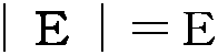 である。ターンオフの場合、ドリフト領域18の空乏層内部における電子濃度とアクセプタ濃度は十分小さいため、無視している。即ち、角部111の近傍において、上面のx-y平面の電界の湾曲により、電界強度Eの傾き(divE)が増加する。そのため、電界強度Eそのものも増加する。よって、E(R)は、角部111に近づくほど、Emから増加する。
ここでqは電荷素量、ε0は真空の誘電率、εrは比誘電率、pは正孔濃度、NDはドナー濃度である。
以上により、電界強度E(R)はRの指数関数に従うと考えられる。角部111でピーク電界強度Epに達すると、電界強度E(R)は次式で示される。
E(R)=Ep×exp(-R/ΔR)+Em ・・・式(2)
Epは角部111におけるピーク電界強度、ΔRは電界強度が減衰する特徴的長さである。Epは、一例として臨界電界強度であってよい。本例では、Epを6E5(V/cm)としている。ΔRは、一例として200μm~400μm程度である。本例のΔRは、300μmである。ただし、ΔRはこの範囲に限られない。
E(R)=Ep×exp(-R/ΔR)+Em ・・・式(2)
Epは角部111におけるピーク電界強度、ΔRは電界強度が減衰する特徴的長さである。Epは、一例として臨界電界強度であってよい。本例では、Epを6E5(V/cm)としている。ΔRは、一例として200μm~400μm程度である。本例のΔRは、300μmである。ただし、ΔRはこの範囲に限られない。
x-y平面の電界のゆがみが無い場合、E(R)は平面接合近似の値Emとなる。Emは、ドリフト層の平均的なドナー濃度をND0、印加電圧をVとして、ポアソンの式からEmが次式で示される。
Em={2V(q/(ε0εr)(p+ND0)}0.5 ・・・式(3)
正孔濃度pについては、例えばトランジスタ部70がターンオフする場合を想定し、ここでは定格電流Jrate程度の電流が流れている場合を想定している。ターンオフでは電圧が印加されているので、空乏層(即ち、空間電荷領域)内の正孔の速度はvsatで飽和しているとしてよく、正孔濃度pが次の式(4)を満たす。
p=Jrate/(qvsat) ・・・式(4)
vsatは、例えばシリコン中の正孔では8×10⁶(cm/s)である。本例では、ND0=5E13/cm3、印加電圧V=600V、定格電流密度Jrate=500A/cm2とし、Emは2.83E5(V/cm)である。
Em={2V(q/(ε0εr)(p+ND0)}0.5 ・・・式(3)
正孔濃度pについては、例えばトランジスタ部70がターンオフする場合を想定し、ここでは定格電流Jrate程度の電流が流れている場合を想定している。ターンオフでは電圧が印加されているので、空乏層(即ち、空間電荷領域)内の正孔の速度はvsatで飽和しているとしてよく、正孔濃度pが次の式(4)を満たす。
p=Jrate/(qvsat) ・・・式(4)
vsatは、例えばシリコン中の正孔では8×10⁶(cm/s)である。本例では、ND0=5E13/cm3、印加電圧V=600V、定格電流密度Jrate=500A/cm2とし、Emは2.83E5(V/cm)である。
図6Aは、角部111から距離R離れた位置における電界強度E(R)の距離R依存性を示す図である。縦軸は電界強度E(R)(V/cm)および最大電界強度Emで規格化した比E(R)/Emを示し、横軸は角部111からの距離R(μm)を示す。
電解強度E(R)は、距離Rが1500μm以上の範囲では、最大電界強度Em程度の電界強度を示す。一方、電解強度E(R)は、距離Rが1500μmよりも短くなるにつれて急激に上昇する。距離Rが1500μmよりも短くなると、電界強度の比E(R)/Emが、1.1以上となる。アバランシェ降伏は臨界的な現象であり、インパクト・イオン化係数は電界強度に強く依存する。そのため、電界強度比E(R)/Emが1.1倍以上になると、インパクト・イオン化係数は2倍以上になり、インパクト・イオン化率が上昇し、アバランシェ降伏が強く発生する。電界強度比E(R)/Emは、距離Rが1000μmよりも小さい場合に1.1以上となる。即ち、距離Rが1000μmよりも短い領域では、1000μm以上の領域よりも、アバランシェ降伏が起きやすいといえる。さらに、距離Rが1500μm以上の場合に、電界強度比E(R)/Emが1.01以下となる。即ち、距離Rが1500μm以上の領域では、電界の空間的歪み(湾曲)による電界強度の増加は十分小さいといえる。以上により、アバランシェ降伏のインパクト・イオン化率は、距離Rが1000μmよりも短い領域で高くなる。本例では、角部111(R=0)で最も高いとしている。
ここで、距離Rを、角部111からトレンチ中央位置TPまでの最短距離R1aに置き換えてよい。即ち、角部111からトレンチ中央位置TPまでの最短距離R1aは、1000μm以上であってよく、1500μm以上であってよい。なお、本例では、距離Rを最短距離R1aに置き換えて説明するが、最短距離R1b、最短距離R2aまたは最短距離R2bについても置き換えて説明することもできる。
ターンオフ時にゲート電圧が+から-にオフすると、電位はゲート金属層50からゲート導電部44に伝わる。ゲート導電部44がポリシリコンの場合、アルミニウム合金等に比べて抵抗率が高い。一方、MOSゲートの反転層消滅(または生成)には、MOSキャパシタの充放電が必要である。MOSキャパシタの充放電には、ゲート絶縁膜42の厚さで決まる静電容量とゲート導電部44の抵抗により、遅延時間が生じる。ゲート金属層50の位置からトレンチ中央位置TPまでの長さが長い程、ゲート導電部44の抵抗が大きくなる。このため、トレンチ中央位置TPのMOSキャパシタの充電に必要な遅延時間が長くなる。この遅延時間の増加により、トレンチ中央位置TP近傍のゲートをオフするのが遅くなり、トレンチ中央位置TPにキャリアが集中して、カレント・フィラメントが発生する。一方、ターンオフのときにはドリフト領域18に空乏層が広がっており、カレント・フィラメントは空乏層の中に存在する。カレント・フィラメントにはキャリア(正孔)が多く残留しているので、空乏層の電界強度の傾きが増加し、電界強度が増加する。さらに、電流密度(特に正孔電流)が大きいので、インパクト・イオン化率も増加させ、アバランシェ降伏が増強される。
トレンチ中央位置TPが角部111から1000μmよりも短い領域に位置すると、最短距離R1aが1000μmよりも短くなる。この場合、ターンオフにおいて、トレンチ中央位置TPにおける電界強度E(R1a)はEmの1.1倍よりも高くなる。このため、トレンチ中央位置TPではカレント・フィラメントだけでなく、電界の空間的歪みによっても電界強度が増加する。すると、角部111の近傍だけでなく、トレンチ中央位置TPにおいてもインパクト・イオン化率が上昇し、アバランシェ降伏が生じ易くなる。その結果、角部111およびトレンチ中央位置Tpを含む領域で電流が正帰還を起こし、破壊に至る可能性が高くなる。よって、最短距離R1aを1000μmよりも長くすることで、トレンチ中央位置TPにおける角部111からの距離Rを1000μm以上とする。これにより、電界強度E(R1a)をEmの1.1倍よりも小さくし、角部111およびトレンチ中央位置TPにおけるアバランシェ降伏の増強を抑えることができ、ターンオフ時の破壊を防ぐことができる。さらに、最短距離R1aを1500μm以上としてよい。
また、導電部形状比αが大きいほど、ゲート導電部44の幅Wgは小さく、トレンチ長さLtが長くなるため、ゲート金属層50の位置からトレンチ中央位置TPまでのゲート導電部44の抵抗が大きくなる。即ち、トレンチ中央位置TP近傍におけるゲート導電部44の充放電に遅延時間が生じ、カレント・フィラメントが発生しやすくなる。よって、上述の導電部形状比αの範囲であって、最短距離R1aを1000μm以上とする。これにより、角部111およびトレンチ中央位置TPにおけるアバランシェ降伏の増強を抑えることができ、ターンオフ時の破壊を防ぐことができる。最短距離R1aは、1500μm以上であってよく、2000μm以上であってよく、3000μm以上であってよく、5000μm以上であってよい。最短距離R1aは、20000μm以下であってよく、15000μm以下であってよく、10000μm以上であってよい。
図6Bは、最短距離R1aとターンオフ耐量の不良率(%)との関係を示すグラフである。ターンオフ耐量の不良率とは、ターンオフにより半導体装置が破壊する割合である。ターンオフの電流密度および印加電圧はさまざまでよく、一例として上述の条件であってよい。本例では、導電部形状比αが6250の場合と、導電部形状比αが8750の場合のターンオフ耐量の不良率を示している。
導電部形状比αが6250の場合、トレンチ長さLtは5000μmであり、ゲート導電部44の幅Wgが0.8μmである。最短距離R1aが500μmの場合、ターンオフ耐量の不良率は50%である。不良率は、最短距離R1aが1000μmで14%へ減少し、最短距離R1aが1500μmで5%、最短距離R1aが2000μmで2%である。
導電部形状比αが8750の場合、トレンチ長さLtが7000μmであり、ゲート導電部44の幅Wgが0.8μmである。最短距離R1aが500μmの場合にターンオフ耐量の不良率は62%で、最短距離R1aが1000μmで21%へ減少する。さらに最短距離R1aが1500μm以上で8%以下まで不良率が大きく減少する。ターンオフ耐量の不良率を30%より低くできることから、最短距離R1aは1000μm以上かそれよりも長くてよく、1500μm以上であってよく、2000μm以上であってよく、3000μm以上であってよく、5000μm以上であってよい。なお、本例では、最短距離R1aについて説明したが、最短距離R1b、最短距離R2aまたは最短距離R2bについても同様に説明することができる。
図6Cは、定格電圧Vrateと定格電流密度Jrateとの関係を示すグラフである。縦軸は定格電流密度Jrate(A/cm2)を示し、横軸は定格電圧(V)を示す。一例において、半導体装置100は、図6Cの上限P1および下限P2で挟まれた領域の定格電圧Vrateおよび定格電流密度Jrateを満たすように設計されてよい。
例えば、半導体装置100は、定格電圧600(V)において、400(A/cm2)以上、800(A/cm2)以下の定格電流密度を満たすように設計されてよい。また、半導体装置100は、定格電圧1200(V)において、300(A/cm2)以上、600(A/cm2)以下の定格電流密度を満たすように設計されてよい。半導体装置100は、定格電圧1700(V)において、200(A/cm2)以上、400(A/cm2)以下の定格電流密度を満たすように設計されてよい。
本例の半導体装置100は、このような特性を実現するためにトレンチ長さLtを2000μm以上としたような場合であっても、P型のウェル領域とトレンチ中央位置TPとの距離を適切に設定することにより、P型のウェル領域へのカレント・フィラメントの流入による素子破壊を回避することができる。
以上、本発明を実施の形態を用いて説明したが、本発明の技術的範囲は上記実施の形態に記載の範囲には限定されない。上記実施の形態に、多様な変更または改良を加えることが可能であることが当業者に明らかである。その様な変更または改良を加えた形態も本発明の技術的範囲に含まれ得ることが、請求の範囲の記載から明らかである。
請求の範囲、明細書、および図面中において示した装置、および方法における動作、手順、ステップ、および段階等の各処理の実行順序は、特段「より前に」、「先立って」等と明示しておらず、また、前の処理の出力を後の処理で用いるのでない限り、任意の順序で実現しうることに留意すべきである。請求の範囲、明細書、および図面中の動作フローに関して、便宜上「まず、」、「次に、」等を用いて説明したとしても、この順で実施することが必須であることを意味するものではない。
10・・・半導体基板、12・・・エミッタ領域、14・・・ベース領域、15・・・コンタクト領域、16・・・蓄積領域、18・・・ドリフト領域、20・・・バッファ領域、21・・・おもて面、22・・・コレクタ領域、23・・・裏面、24・・・コレクタ電極、25・・・接続部、30・・・ダミートレンチ部、31・・・延伸部分、32・・・ダミー絶縁膜、33・・・接続部分、34・・・ダミー導電部、38・・・層間絶縁膜、40・・・ゲートトレンチ部、41・・・延伸部分、42・・・ゲート絶縁膜、43・・・接続部分、44・・・ゲート導電部、50・・・ゲート金属層、52・・・エミッタ電極、54・・・コンタクトホール、55・・・コンタクトホール、56・・・コンタクトホール、70・・・トランジスタ部、71・・・メサ部、80・・・ダイオード部、81・・・メサ部、82・・・カソード領域、90・・・境界部、91・・・メサ部、92・・・境界部、100・・・半導体装置、102・・・活性部、104・・・外周部、110・・・第1制御パッド、111・・・角部、112・・・アノードパッド、114・・・カソードパッド、115・・・ウェル領域、116・・・センスパッド、118・・・切欠部、120・・・第2制御パッド、121・・・角部、122・・・ゲートパッド、125・・・ウェル領域、130・・・ライフタイム制御領域、135・・・ウェル領域、140・・・温度センス部、142・・・温度センス配線、145・・・ウェル領域、150・・・外周端、151・・・第1外周辺、152・・・第2外周辺、170・・・無効領域、172・・・ダミートレンチ領域、180・・・保護膜、185・・・非保護領域
Claims (20)
- 半導体基板に設けられた活性部と、
ゲート導電部を有し、前記活性部において、予め定められた延伸方向に延伸して設けられ、予め定められた配列方向に配列された複数のトレンチ部であって、前記延伸方向におけるトレンチ長さに対する、前記ゲート導電部の前記配列方向における幅の導電部形状比が1000以上である複数のトレンチ部と、
上面視において、前記半導体基板の予め定められた第1外周辺から前記半導体基板の内側に張り出して設けられた第1制御パッドと、
前記第1制御パッドの下方に設けられ、上面視において前記第1制御パッドを覆って設けられた第1ウェル領域と
を備え、
上面視において、前記第1ウェル領域と、前記複数のトレンチ部の前記延伸方向における長さの中央であるトレンチ中央位置との間の最短距離が1000μm以上である
半導体装置。 - 前記最短距離は、1500μm以上である
請求項1に記載の半導体装置。 - 前記最短距離は、2000μm以上である
請求項1または2に記載の半導体装置。 - 前記複数のトレンチ部の前記導電部形状比は、3000以上、1×10⁶以下である
請求項1から3のいずれか一項に記載の半導体装置。 - 前記複数のトレンチ部は、ゲート電位に設定されたゲートトレンチ部を含み、
前記ゲートトレンチ部の前記導電部形状比は、5000以上、3×10⁵以下である
請求項1から4のいずれか一項に記載の半導体装置。 - 前記第1制御パッドは、アノードパッド、カソードパッドおよびセンスパッドを含む
請求項1から4のいずれか一項に記載の半導体装置。 - 前記第1ウェル領域は、上面視で矩形を有し、前記第1ウェル領域の3辺が前記活性部と対向して設けられる
請求項1から6のいずれか一項に記載の半導体装置。 - 前記第1ウェル領域は、前記第1外周辺から張り出して設けられた角部を有し、
前記最短距離は、前記第1ウェル領域の前記角部と、前記トレンチ中央位置との距離である
請求項1から7のいずれか一項に記載の半導体装置。 - 前記第1外周辺と直交し、前記第1外周辺の中央を通る中央仮想線から、前記第1ウェル領域の前記角部までの距離L1aは、前記中央仮想線と直交する方向における前記中央仮想線から前記半導体基板の外周端までの長さの40%以上である
請求項8に記載の半導体装置。 - 前記第1ウェル領域は、前記第1外周辺と直交して前記第1外周辺の中央を通る中央仮想線に対して対称に設けられる
請求項1から9のいずれか一項に記載の半導体装置。 - 前記第1ウェル領域は、前記第1外周辺と直交して前記第1外周辺の中央を通る中央仮想線に対して非対称に設けられる
請求項1から9のいずれか一項に記載の半導体装置。 - 前記第1ウェル領域は、上面視において、角の一部が切り取られた切欠部を備える
請求項1から11のいずれか一項に記載の半導体装置。 - 上面視において、前記第1外周辺と対向する第2外周辺から前記半導体基板の内側に張り出して設けられた第2制御パッドと、
前記第2制御パッドの下方に設けられ、上面視において前記第2制御パッドを覆って設けられた第2ウェル領域と
を備え、
前記第2ウェル領域は、前記第2外周辺から張り出して設けられた角部を有し、
前記距離L1aは、前記延伸方向における前記中央仮想線から前記第2ウェル領域の角部までの距離L2aより長い
請求項9に記載の半導体装置。 - 前記第2制御パッドは、前記複数のトレンチ部をゲート電位に設定するためのゲートパッドを含む
請求項13に記載の半導体装置。 - 前記活性部は、トランジスタ部およびダイオード部を備え、
前記第1ウェル領域の角部は、上面視において、前記トランジスタ部に位置する
請求項1から14のいずれか一項に記載の半導体装置。 - 前記複数のトレンチ部がエミッタ電位に設定されたダミートレンチ領域を備え、
前記第1ウェル領域の角部は、上面視において、前記ダミートレンチ領域に位置する
請求項1から14のいずれか一項に記載の半導体装置。 - 前記活性部は、トランジスタ部およびダイオード部を備え、
前記第1ウェル領域の角部は、上面視において、前記ダイオード部に位置する
請求項1から14のいずれか一項に記載の半導体装置。 - 前記半導体基板の上方に設けられた保護膜を備え、
前記ダイオード部は、前記半導体基板のおもて面側にライフタイム制御領域を有し、
前記保護膜は、上面視において、前記ダイオード部を避けて設けられる
請求項17に記載の半導体装置。 - 前記延伸方向は、上面視において、前記第1外周辺と平行である
請求項1から18のいずれか一項に記載の半導体装置。 - 前記延伸方向は、上面視において、前記第1外周辺と直交する
請求項1から18のいずれか一項に記載の半導体装置。
Priority Applications (4)
| Application Number | Priority Date | Filing Date | Title |
|---|---|---|---|
| CN202180024457.4A CN115398645A (zh) | 2020-10-16 | 2021-10-15 | 半导体装置 |
| JP2022557495A JP7396513B2 (ja) | 2020-10-16 | 2021-10-15 | 半導体装置 |
| DE112021000878.1T DE112021000878T5 (de) | 2020-10-16 | 2021-10-15 | Halbleitervorrichtung |
| US17/948,258 US12550348B2 (en) | 2020-10-16 | 2022-09-20 | Semiconductor device |
Applications Claiming Priority (2)
| Application Number | Priority Date | Filing Date | Title |
|---|---|---|---|
| JP2020-174399 | 2020-10-16 | ||
| JP2020174399 | 2020-10-16 |
Related Child Applications (1)
| Application Number | Title | Priority Date | Filing Date |
|---|---|---|---|
| US17/948,258 Continuation US12550348B2 (en) | 2020-10-16 | 2022-09-20 | Semiconductor device |
Publications (1)
| Publication Number | Publication Date |
|---|---|
| WO2022080495A1 true WO2022080495A1 (ja) | 2022-04-21 |
Family
ID=81208148
Family Applications (1)
| Application Number | Title | Priority Date | Filing Date |
|---|---|---|---|
| PCT/JP2021/038317 Ceased WO2022080495A1 (ja) | 2020-10-16 | 2021-10-15 | 半導体装置 |
Country Status (5)
| Country | Link |
|---|---|
| US (1) | US12550348B2 (ja) |
| JP (1) | JP7396513B2 (ja) |
| CN (1) | CN115398645A (ja) |
| DE (1) | DE112021000878T5 (ja) |
| WO (1) | WO2022080495A1 (ja) |
Citations (3)
| Publication number | Priority date | Publication date | Assignee | Title |
|---|---|---|---|---|
| JP2019161199A (ja) * | 2017-05-17 | 2019-09-19 | ローム株式会社 | 半導体装置 |
| JP2019186309A (ja) * | 2018-04-04 | 2019-10-24 | 富士電機株式会社 | 半導体装置 |
| WO2020162013A1 (ja) * | 2019-02-07 | 2020-08-13 | 富士電機株式会社 | 半導体装置 |
Family Cites Families (31)
| Publication number | Priority date | Publication date | Assignee | Title |
|---|---|---|---|---|
| JP3410949B2 (ja) | 1998-02-12 | 2003-05-26 | 株式会社東芝 | 半導体装置 |
| JP2001015738A (ja) * | 1999-06-29 | 2001-01-19 | Toshiba Corp | 半導体装置 |
| JP5167741B2 (ja) | 2007-09-21 | 2013-03-21 | 株式会社デンソー | 半導体装置 |
| US8022470B2 (en) * | 2008-09-04 | 2011-09-20 | Infineon Technologies Austria Ag | Semiconductor device with a trench gate structure and method for the production thereof |
| CN105210187B (zh) * | 2013-10-04 | 2017-10-10 | 富士电机株式会社 | 半导体装置 |
| US10217738B2 (en) * | 2015-05-15 | 2019-02-26 | Smk Corporation | IGBT semiconductor device |
| US10332990B2 (en) * | 2015-07-15 | 2019-06-25 | Fuji Electric Co., Ltd. | Semiconductor device |
| US10056370B2 (en) * | 2015-07-16 | 2018-08-21 | Fuji Electric Co., Ltd. | Semiconductor device |
| CN107086217B (zh) * | 2016-02-16 | 2023-05-16 | 富士电机株式会社 | 半导体装置 |
| CN108604602B (zh) * | 2016-08-12 | 2021-06-15 | 富士电机株式会社 | 半导体装置及半导体装置的制造方法 |
| JP6881463B2 (ja) * | 2016-09-14 | 2021-06-02 | 富士電機株式会社 | Rc−igbtおよびその製造方法 |
| US10559663B2 (en) * | 2016-10-14 | 2020-02-11 | Fuji Electric Co., Ltd. | Semiconductor device with improved current flow distribution |
| EP3324443B1 (en) * | 2016-11-17 | 2019-09-11 | Fuji Electric Co., Ltd. | Semiconductor device |
| WO2018154963A1 (ja) | 2017-02-24 | 2018-08-30 | 富士電機株式会社 | 半導体装置 |
| JP7020185B2 (ja) | 2017-03-15 | 2022-02-16 | 富士電機株式会社 | 半導体装置 |
| JP7013668B2 (ja) * | 2017-04-06 | 2022-02-01 | 富士電機株式会社 | 半導体装置 |
| JP7325931B2 (ja) * | 2017-05-16 | 2023-08-15 | 富士電機株式会社 | 半導体装置 |
| US10396189B2 (en) * | 2017-05-30 | 2019-08-27 | Fuji Electric Co., Ltd. | Semiconductor device |
| JP6835243B2 (ja) | 2017-10-18 | 2021-02-24 | 富士電機株式会社 | 半導体装置 |
| JP2019114643A (ja) * | 2017-12-22 | 2019-07-11 | ルネサスエレクトロニクス株式会社 | 半導体装置およびその製造方法 |
| JP7095303B2 (ja) * | 2018-02-14 | 2022-07-05 | 富士電機株式会社 | 半導体装置 |
| JP7073773B2 (ja) | 2018-02-15 | 2022-05-24 | 富士電機株式会社 | 半導体装置 |
| JP7091693B2 (ja) * | 2018-02-19 | 2022-06-28 | 富士電機株式会社 | 半導体装置 |
| CN117936538A (zh) | 2018-03-15 | 2024-04-26 | 富士电机株式会社 | 半导体装置 |
| JP7206652B2 (ja) | 2018-03-30 | 2023-01-18 | 富士電機株式会社 | 半導体装置、半導体パッケージ、半導体モジュール、および半導体回路装置 |
| WO2019244485A1 (ja) | 2018-06-22 | 2019-12-26 | 富士電機株式会社 | 半導体装置の製造方法および半導体装置 |
| JP7268330B2 (ja) | 2018-11-05 | 2023-05-08 | 富士電機株式会社 | 半導体装置および製造方法 |
| US11450734B2 (en) * | 2019-06-17 | 2022-09-20 | Fuji Electric Co., Ltd. | Semiconductor device and fabrication method for semiconductor device |
| JP2021012995A (ja) | 2019-07-09 | 2021-02-04 | トヨタ自動車株式会社 | トレンチゲート型半導体装置 |
| JP7242491B2 (ja) * | 2019-09-20 | 2023-03-20 | 株式会社東芝 | 半導体装置及び半導体回路 |
| US11075291B1 (en) * | 2020-04-09 | 2021-07-27 | Infineon Technologies Austria Ag | Isolation structure for IGBT devices having an integrated diode |
-
2021
- 2021-10-15 JP JP2022557495A patent/JP7396513B2/ja active Active
- 2021-10-15 CN CN202180024457.4A patent/CN115398645A/zh active Pending
- 2021-10-15 DE DE112021000878.1T patent/DE112021000878T5/de active Pending
- 2021-10-15 WO PCT/JP2021/038317 patent/WO2022080495A1/ja not_active Ceased
-
2022
- 2022-09-20 US US17/948,258 patent/US12550348B2/en active Active
Patent Citations (3)
| Publication number | Priority date | Publication date | Assignee | Title |
|---|---|---|---|---|
| JP2019161199A (ja) * | 2017-05-17 | 2019-09-19 | ローム株式会社 | 半導体装置 |
| JP2019186309A (ja) * | 2018-04-04 | 2019-10-24 | 富士電機株式会社 | 半導体装置 |
| WO2020162013A1 (ja) * | 2019-02-07 | 2020-08-13 | 富士電機株式会社 | 半導体装置 |
Also Published As
| Publication number | Publication date |
|---|---|
| US20230019632A1 (en) | 2023-01-19 |
| JPWO2022080495A1 (ja) | 2022-04-21 |
| DE112021000878T5 (de) | 2022-11-24 |
| JP7396513B2 (ja) | 2023-12-12 |
| CN115398645A (zh) | 2022-11-25 |
| US12550348B2 (en) | 2026-02-10 |
Similar Documents
| Publication | Publication Date | Title |
|---|---|---|
| US12218024B2 (en) | Semiconductor device and fabrication method thereof | |
| US11532738B2 (en) | Semiconductor device | |
| US12593500B2 (en) | Semiconductor device | |
| JP7497744B2 (ja) | 半導体装置 | |
| JPWO2019116696A1 (ja) | 半導体装置 | |
| JPWO2019111572A1 (ja) | 半導体装置 | |
| CN107833914A (zh) | 半导体装置 | |
| JP7456113B2 (ja) | 半導体装置 | |
| US12495564B2 (en) | Semiconductor device | |
| US11424351B2 (en) | Semiconductor device and method of manufacturing semiconductor device | |
| JP7231065B2 (ja) | 半導体装置 | |
| US20230402533A1 (en) | Semiconductor device | |
| US20260013164A1 (en) | Semiconductor device | |
| US12288787B2 (en) | Semiconductor device | |
| US20240363623A1 (en) | Semiconductor device | |
| WO2022239284A1 (ja) | 半導体装置 | |
| JP6658955B2 (ja) | 半導体装置 | |
| JP2022161688A (ja) | 半導体装置 | |
| US12183789B2 (en) | Semiconductor device | |
| US20240243191A1 (en) | Semiconductor device | |
| JP7732510B2 (ja) | 半導体装置 | |
| JP7396513B2 (ja) | 半導体装置 | |
| US20250218780A1 (en) | Fabrication method of semiconductor device | |
| WO2024262142A1 (ja) | 半導体装置および半導体装置の製造方法 | |
| JP2024100692A (ja) | 半導体装置 |
Legal Events
| Date | Code | Title | Description |
|---|---|---|---|
| 121 | Ep: the epo has been informed by wipo that ep was designated in this application |
Ref document number: 21880230 Country of ref document: EP Kind code of ref document: A1 |
|
| ENP | Entry into the national phase |
Ref document number: 2022557495 Country of ref document: JP Kind code of ref document: A |
|
| 122 | Ep: pct application non-entry in european phase |
Ref document number: 21880230 Country of ref document: EP Kind code of ref document: A1 |