WO2021177348A1 - 光学積層体の製造方法 - Google Patents
光学積層体の製造方法 Download PDFInfo
- Publication number
- WO2021177348A1 WO2021177348A1 PCT/JP2021/008165 JP2021008165W WO2021177348A1 WO 2021177348 A1 WO2021177348 A1 WO 2021177348A1 JP 2021008165 W JP2021008165 W JP 2021008165W WO 2021177348 A1 WO2021177348 A1 WO 2021177348A1
- Authority
- WO
- WIPO (PCT)
- Prior art keywords
- layer
- optical
- optical functional
- functional layer
- antifouling
- Prior art date
- Legal status (The legal status is an assumption and is not a legal conclusion. Google has not performed a legal analysis and makes no representation as to the accuracy of the status listed.)
- Ceased
Links
Images

Classifications
-
- B—PERFORMING OPERATIONS; TRANSPORTING
- B32—LAYERED PRODUCTS
- B32B—LAYERED PRODUCTS, i.e. PRODUCTS BUILT-UP OF STRATA OF FLAT OR NON-FLAT, e.g. CELLULAR OR HONEYCOMB, FORM
- B32B7/00—Layered products characterised by the relation between layers; Layered products characterised by the relative orientation of features between layers, or by the relative values of a measurable parameter between layers, i.e. products comprising layers having different physical, chemical or physicochemical properties; Layered products characterised by the interconnection of layers
- B32B7/02—Physical, chemical or physicochemical properties
- B32B7/023—Optical properties
-
- G—PHYSICS
- G02—OPTICS
- G02B—OPTICAL ELEMENTS, SYSTEMS OR APPARATUS
- G02B1/00—Optical elements characterised by the material of which they are made; Optical coatings for optical elements
- G02B1/10—Optical coatings produced by application to, or surface treatment of, optical elements
- G02B1/11—Anti-reflection coatings
-
- B—PERFORMING OPERATIONS; TRANSPORTING
- B32—LAYERED PRODUCTS
- B32B—LAYERED PRODUCTS, i.e. PRODUCTS BUILT-UP OF STRATA OF FLAT OR NON-FLAT, e.g. CELLULAR OR HONEYCOMB, FORM
- B32B15/00—Layered products comprising a layer of metal
- B32B15/04—Layered products comprising a layer of metal comprising metal as the main or only constituent of a layer, which is next to another layer of the same or of a different material
-
- B—PERFORMING OPERATIONS; TRANSPORTING
- B32—LAYERED PRODUCTS
- B32B—LAYERED PRODUCTS, i.e. PRODUCTS BUILT-UP OF STRATA OF FLAT OR NON-FLAT, e.g. CELLULAR OR HONEYCOMB, FORM
- B32B27/00—Layered products comprising a layer of synthetic resin
- B32B27/18—Layered products comprising a layer of synthetic resin characterised by the use of special additives
- B32B27/20—Layered products comprising a layer of synthetic resin characterised by the use of special additives using fillers, pigments, thixotroping agents
-
- B—PERFORMING OPERATIONS; TRANSPORTING
- B32—LAYERED PRODUCTS
- B32B—LAYERED PRODUCTS, i.e. PRODUCTS BUILT-UP OF STRATA OF FLAT OR NON-FLAT, e.g. CELLULAR OR HONEYCOMB, FORM
- B32B33/00—Layered products characterised by particular properties or particular surface features, e.g. particular surface coatings; Layered products designed for particular purposes not covered by another single class
-
- B—PERFORMING OPERATIONS; TRANSPORTING
- B32—LAYERED PRODUCTS
- B32B—LAYERED PRODUCTS, i.e. PRODUCTS BUILT-UP OF STRATA OF FLAT OR NON-FLAT, e.g. CELLULAR OR HONEYCOMB, FORM
- B32B37/00—Methods or apparatus for laminating, e.g. by curing or by ultrasonic bonding
- B32B37/14—Methods or apparatus for laminating, e.g. by curing or by ultrasonic bonding characterised by the properties of the layers
- B32B37/144—Methods or apparatus for laminating, e.g. by curing or by ultrasonic bonding characterised by the properties of the layers using layers with different mechanical or chemical conditions or properties, e.g. layers with different thermal shrinkage, layers under tension during bonding
-
- B—PERFORMING OPERATIONS; TRANSPORTING
- B32—LAYERED PRODUCTS
- B32B—LAYERED PRODUCTS, i.e. PRODUCTS BUILT-UP OF STRATA OF FLAT OR NON-FLAT, e.g. CELLULAR OR HONEYCOMB, FORM
- B32B37/00—Methods or apparatus for laminating, e.g. by curing or by ultrasonic bonding
- B32B37/14—Methods or apparatus for laminating, e.g. by curing or by ultrasonic bonding characterised by the properties of the layers
- B32B37/24—Methods or apparatus for laminating, e.g. by curing or by ultrasonic bonding characterised by the properties of the layers with at least one layer not being coherent before laminating, e.g. made up from granular material sprinkled onto a substrate
-
- B—PERFORMING OPERATIONS; TRANSPORTING
- B32—LAYERED PRODUCTS
- B32B—LAYERED PRODUCTS, i.e. PRODUCTS BUILT-UP OF STRATA OF FLAT OR NON-FLAT, e.g. CELLULAR OR HONEYCOMB, FORM
- B32B38/00—Ancillary operations in connection with laminating processes
- B32B38/0008—Electrical discharge treatment, e.g. corona, plasma treatment; wave energy or particle radiation
-
- B—PERFORMING OPERATIONS; TRANSPORTING
- B32—LAYERED PRODUCTS
- B32B—LAYERED PRODUCTS, i.e. PRODUCTS BUILT-UP OF STRATA OF FLAT OR NON-FLAT, e.g. CELLULAR OR HONEYCOMB, FORM
- B32B38/00—Ancillary operations in connection with laminating processes
- B32B38/18—Handling of layers or the laminate
- B32B38/1858—Handling of layers or the laminate using vacuum
-
- B—PERFORMING OPERATIONS; TRANSPORTING
- B32—LAYERED PRODUCTS
- B32B—LAYERED PRODUCTS, i.e. PRODUCTS BUILT-UP OF STRATA OF FLAT OR NON-FLAT, e.g. CELLULAR OR HONEYCOMB, FORM
- B32B7/00—Layered products characterised by the relation between layers; Layered products characterised by the relative orientation of features between layers, or by the relative values of a measurable parameter between layers, i.e. products comprising layers having different physical, chemical or physicochemical properties; Layered products characterised by the interconnection of layers
- B32B7/04—Interconnection of layers
- B32B7/12—Interconnection of layers using interposed adhesives or interposed materials with bonding properties
-
- B—PERFORMING OPERATIONS; TRANSPORTING
- B32—LAYERED PRODUCTS
- B32B—LAYERED PRODUCTS, i.e. PRODUCTS BUILT-UP OF STRATA OF FLAT OR NON-FLAT, e.g. CELLULAR OR HONEYCOMB, FORM
- B32B9/00—Layered products comprising a layer of a particular substance not covered by groups B32B11/00 - B32B29/00
-
- B—PERFORMING OPERATIONS; TRANSPORTING
- B32—LAYERED PRODUCTS
- B32B—LAYERED PRODUCTS, i.e. PRODUCTS BUILT-UP OF STRATA OF FLAT OR NON-FLAT, e.g. CELLULAR OR HONEYCOMB, FORM
- B32B9/00—Layered products comprising a layer of a particular substance not covered by groups B32B11/00 - B32B29/00
- B32B9/04—Layered products comprising a layer of a particular substance not covered by groups B32B11/00 - B32B29/00 comprising such particular substance as the main or only constituent of a layer, which is next to another layer of the same or of a different material
- B32B9/041—Layered products comprising a layer of a particular substance not covered by groups B32B11/00 - B32B29/00 comprising such particular substance as the main or only constituent of a layer, which is next to another layer of the same or of a different material of metal
-
- C—CHEMISTRY; METALLURGY
- C23—COATING METALLIC MATERIAL; COATING MATERIAL WITH METALLIC MATERIAL; CHEMICAL SURFACE TREATMENT; DIFFUSION TREATMENT OF METALLIC MATERIAL; COATING BY VACUUM EVAPORATION, BY SPUTTERING, BY ION IMPLANTATION OR BY CHEMICAL VAPOUR DEPOSITION, IN GENERAL; INHIBITING CORROSION OF METALLIC MATERIAL OR INCRUSTATION IN GENERAL
- C23C—COATING METALLIC MATERIAL; COATING MATERIAL WITH METALLIC MATERIAL; SURFACE TREATMENT OF METALLIC MATERIAL BY DIFFUSION INTO THE SURFACE, BY CHEMICAL CONVERSION OR SUBSTITUTION; COATING BY VACUUM EVAPORATION, BY SPUTTERING, BY ION IMPLANTATION OR BY CHEMICAL VAPOUR DEPOSITION, IN GENERAL
- C23C14/00—Coating by vacuum evaporation, by sputtering or by ion implantation of the coating forming material
- C23C14/02—Pretreatment of the material to be coated
- C23C14/024—Deposition of sublayers, e.g. to promote adhesion of the coating
-
- C—CHEMISTRY; METALLURGY
- C23—COATING METALLIC MATERIAL; COATING MATERIAL WITH METALLIC MATERIAL; CHEMICAL SURFACE TREATMENT; DIFFUSION TREATMENT OF METALLIC MATERIAL; COATING BY VACUUM EVAPORATION, BY SPUTTERING, BY ION IMPLANTATION OR BY CHEMICAL VAPOUR DEPOSITION, IN GENERAL; INHIBITING CORROSION OF METALLIC MATERIAL OR INCRUSTATION IN GENERAL
- C23C—COATING METALLIC MATERIAL; COATING MATERIAL WITH METALLIC MATERIAL; SURFACE TREATMENT OF METALLIC MATERIAL BY DIFFUSION INTO THE SURFACE, BY CHEMICAL CONVERSION OR SUBSTITUTION; COATING BY VACUUM EVAPORATION, BY SPUTTERING, BY ION IMPLANTATION OR BY CHEMICAL VAPOUR DEPOSITION, IN GENERAL
- C23C14/00—Coating by vacuum evaporation, by sputtering or by ion implantation of the coating forming material
- C23C14/06—Coating by vacuum evaporation, by sputtering or by ion implantation of the coating forming material characterised by the coating material
- C23C14/08—Oxides
-
- C—CHEMISTRY; METALLURGY
- C23—COATING METALLIC MATERIAL; COATING MATERIAL WITH METALLIC MATERIAL; CHEMICAL SURFACE TREATMENT; DIFFUSION TREATMENT OF METALLIC MATERIAL; COATING BY VACUUM EVAPORATION, BY SPUTTERING, BY ION IMPLANTATION OR BY CHEMICAL VAPOUR DEPOSITION, IN GENERAL; INHIBITING CORROSION OF METALLIC MATERIAL OR INCRUSTATION IN GENERAL
- C23C—COATING METALLIC MATERIAL; COATING MATERIAL WITH METALLIC MATERIAL; SURFACE TREATMENT OF METALLIC MATERIAL BY DIFFUSION INTO THE SURFACE, BY CHEMICAL CONVERSION OR SUBSTITUTION; COATING BY VACUUM EVAPORATION, BY SPUTTERING, BY ION IMPLANTATION OR BY CHEMICAL VAPOUR DEPOSITION, IN GENERAL
- C23C14/00—Coating by vacuum evaporation, by sputtering or by ion implantation of the coating forming material
- C23C14/06—Coating by vacuum evaporation, by sputtering or by ion implantation of the coating forming material characterised by the coating material
- C23C14/10—Glass or silica
-
- C—CHEMISTRY; METALLURGY
- C23—COATING METALLIC MATERIAL; COATING MATERIAL WITH METALLIC MATERIAL; CHEMICAL SURFACE TREATMENT; DIFFUSION TREATMENT OF METALLIC MATERIAL; COATING BY VACUUM EVAPORATION, BY SPUTTERING, BY ION IMPLANTATION OR BY CHEMICAL VAPOUR DEPOSITION, IN GENERAL; INHIBITING CORROSION OF METALLIC MATERIAL OR INCRUSTATION IN GENERAL
- C23C—COATING METALLIC MATERIAL; COATING MATERIAL WITH METALLIC MATERIAL; SURFACE TREATMENT OF METALLIC MATERIAL BY DIFFUSION INTO THE SURFACE, BY CHEMICAL CONVERSION OR SUBSTITUTION; COATING BY VACUUM EVAPORATION, BY SPUTTERING, BY ION IMPLANTATION OR BY CHEMICAL VAPOUR DEPOSITION, IN GENERAL
- C23C14/00—Coating by vacuum evaporation, by sputtering or by ion implantation of the coating forming material
- C23C14/06—Coating by vacuum evaporation, by sputtering or by ion implantation of the coating forming material characterised by the coating material
- C23C14/12—Organic material
-
- C—CHEMISTRY; METALLURGY
- C23—COATING METALLIC MATERIAL; COATING MATERIAL WITH METALLIC MATERIAL; CHEMICAL SURFACE TREATMENT; DIFFUSION TREATMENT OF METALLIC MATERIAL; COATING BY VACUUM EVAPORATION, BY SPUTTERING, BY ION IMPLANTATION OR BY CHEMICAL VAPOUR DEPOSITION, IN GENERAL; INHIBITING CORROSION OF METALLIC MATERIAL OR INCRUSTATION IN GENERAL
- C23C—COATING METALLIC MATERIAL; COATING MATERIAL WITH METALLIC MATERIAL; SURFACE TREATMENT OF METALLIC MATERIAL BY DIFFUSION INTO THE SURFACE, BY CHEMICAL CONVERSION OR SUBSTITUTION; COATING BY VACUUM EVAPORATION, BY SPUTTERING, BY ION IMPLANTATION OR BY CHEMICAL VAPOUR DEPOSITION, IN GENERAL
- C23C14/00—Coating by vacuum evaporation, by sputtering or by ion implantation of the coating forming material
- C23C14/58—After-treatment
- C23C14/5826—Treatment with charged particles
-
- C—CHEMISTRY; METALLURGY
- C23—COATING METALLIC MATERIAL; COATING MATERIAL WITH METALLIC MATERIAL; CHEMICAL SURFACE TREATMENT; DIFFUSION TREATMENT OF METALLIC MATERIAL; COATING BY VACUUM EVAPORATION, BY SPUTTERING, BY ION IMPLANTATION OR BY CHEMICAL VAPOUR DEPOSITION, IN GENERAL; INHIBITING CORROSION OF METALLIC MATERIAL OR INCRUSTATION IN GENERAL
- C23C—COATING METALLIC MATERIAL; COATING MATERIAL WITH METALLIC MATERIAL; SURFACE TREATMENT OF METALLIC MATERIAL BY DIFFUSION INTO THE SURFACE, BY CHEMICAL CONVERSION OR SUBSTITUTION; COATING BY VACUUM EVAPORATION, BY SPUTTERING, BY ION IMPLANTATION OR BY CHEMICAL VAPOUR DEPOSITION, IN GENERAL
- C23C14/00—Coating by vacuum evaporation, by sputtering or by ion implantation of the coating forming material
- C23C14/58—After-treatment
- C23C14/5873—Removal of material
-
- G—PHYSICS
- G02—OPTICS
- G02B—OPTICAL ELEMENTS, SYSTEMS OR APPARATUS
- G02B1/00—Optical elements characterised by the material of which they are made; Optical coatings for optical elements
- G02B1/10—Optical coatings produced by application to, or surface treatment of, optical elements
- G02B1/11—Anti-reflection coatings
- G02B1/113—Anti-reflection coatings using inorganic layer materials only
- G02B1/115—Multilayers
-
- G—PHYSICS
- G02—OPTICS
- G02B—OPTICAL ELEMENTS, SYSTEMS OR APPARATUS
- G02B1/00—Optical elements characterised by the material of which they are made; Optical coatings for optical elements
- G02B1/10—Optical coatings produced by application to, or surface treatment of, optical elements
- G02B1/14—Protective coatings, e.g. hard coatings
-
- G—PHYSICS
- G02—OPTICS
- G02B—OPTICAL ELEMENTS, SYSTEMS OR APPARATUS
- G02B1/00—Optical elements characterised by the material of which they are made; Optical coatings for optical elements
- G02B1/10—Optical coatings produced by application to, or surface treatment of, optical elements
- G02B1/18—Coatings for keeping optical surfaces clean, e.g. hydrophobic or photo-catalytic films
-
- B—PERFORMING OPERATIONS; TRANSPORTING
- B32—LAYERED PRODUCTS
- B32B—LAYERED PRODUCTS, i.e. PRODUCTS BUILT-UP OF STRATA OF FLAT OR NON-FLAT, e.g. CELLULAR OR HONEYCOMB, FORM
- B32B37/00—Methods or apparatus for laminating, e.g. by curing or by ultrasonic bonding
- B32B37/14—Methods or apparatus for laminating, e.g. by curing or by ultrasonic bonding characterised by the properties of the layers
- B32B37/24—Methods or apparatus for laminating, e.g. by curing or by ultrasonic bonding characterised by the properties of the layers with at least one layer not being coherent before laminating, e.g. made up from granular material sprinkled onto a substrate
- B32B2037/243—Coating
-
- B—PERFORMING OPERATIONS; TRANSPORTING
- B32—LAYERED PRODUCTS
- B32B—LAYERED PRODUCTS, i.e. PRODUCTS BUILT-UP OF STRATA OF FLAT OR NON-FLAT, e.g. CELLULAR OR HONEYCOMB, FORM
- B32B37/00—Methods or apparatus for laminating, e.g. by curing or by ultrasonic bonding
- B32B37/14—Methods or apparatus for laminating, e.g. by curing or by ultrasonic bonding characterised by the properties of the layers
- B32B37/24—Methods or apparatus for laminating, e.g. by curing or by ultrasonic bonding characterised by the properties of the layers with at least one layer not being coherent before laminating, e.g. made up from granular material sprinkled onto a substrate
- B32B2037/246—Vapour deposition
-
- B—PERFORMING OPERATIONS; TRANSPORTING
- B32—LAYERED PRODUCTS
- B32B—LAYERED PRODUCTS, i.e. PRODUCTS BUILT-UP OF STRATA OF FLAT OR NON-FLAT, e.g. CELLULAR OR HONEYCOMB, FORM
- B32B2250/00—Layers arrangement
- B32B2250/03—3 layers
-
- B—PERFORMING OPERATIONS; TRANSPORTING
- B32—LAYERED PRODUCTS
- B32B—LAYERED PRODUCTS, i.e. PRODUCTS BUILT-UP OF STRATA OF FLAT OR NON-FLAT, e.g. CELLULAR OR HONEYCOMB, FORM
- B32B2255/00—Coating on the layer surface
- B32B2255/10—Coating on the layer surface on synthetic resin layer or on natural or synthetic rubber layer
-
- B—PERFORMING OPERATIONS; TRANSPORTING
- B32—LAYERED PRODUCTS
- B32B—LAYERED PRODUCTS, i.e. PRODUCTS BUILT-UP OF STRATA OF FLAT OR NON-FLAT, e.g. CELLULAR OR HONEYCOMB, FORM
- B32B2307/00—Properties of the layers or laminate
- B32B2307/40—Properties of the layers or laminate having particular optical properties
- B32B2307/412—Transparent
-
- B—PERFORMING OPERATIONS; TRANSPORTING
- B32—LAYERED PRODUCTS
- B32B—LAYERED PRODUCTS, i.e. PRODUCTS BUILT-UP OF STRATA OF FLAT OR NON-FLAT, e.g. CELLULAR OR HONEYCOMB, FORM
- B32B2307/00—Properties of the layers or laminate
- B32B2307/40—Properties of the layers or laminate having particular optical properties
- B32B2307/418—Refractive
-
- B—PERFORMING OPERATIONS; TRANSPORTING
- B32—LAYERED PRODUCTS
- B32B—LAYERED PRODUCTS, i.e. PRODUCTS BUILT-UP OF STRATA OF FLAT OR NON-FLAT, e.g. CELLULAR OR HONEYCOMB, FORM
- B32B2307/00—Properties of the layers or laminate
- B32B2307/50—Properties of the layers or laminate having particular mechanical properties
- B32B2307/538—Roughness
-
- B—PERFORMING OPERATIONS; TRANSPORTING
- B32—LAYERED PRODUCTS
- B32B—LAYERED PRODUCTS, i.e. PRODUCTS BUILT-UP OF STRATA OF FLAT OR NON-FLAT, e.g. CELLULAR OR HONEYCOMB, FORM
- B32B2307/00—Properties of the layers or laminate
- B32B2307/50—Properties of the layers or laminate having particular mechanical properties
- B32B2307/554—Wear resistance
-
- B—PERFORMING OPERATIONS; TRANSPORTING
- B32—LAYERED PRODUCTS
- B32B—LAYERED PRODUCTS, i.e. PRODUCTS BUILT-UP OF STRATA OF FLAT OR NON-FLAT, e.g. CELLULAR OR HONEYCOMB, FORM
- B32B2307/00—Properties of the layers or laminate
- B32B2307/50—Properties of the layers or laminate having particular mechanical properties
- B32B2307/584—Scratch resistance
-
- B—PERFORMING OPERATIONS; TRANSPORTING
- B32—LAYERED PRODUCTS
- B32B—LAYERED PRODUCTS, i.e. PRODUCTS BUILT-UP OF STRATA OF FLAT OR NON-FLAT, e.g. CELLULAR OR HONEYCOMB, FORM
- B32B2457/00—Electrical equipment
- B32B2457/20—Displays, e.g. liquid crystal displays, plasma displays
- B32B2457/206—Organic displays, e.g. OLED
-
- Y—GENERAL TAGGING OF NEW TECHNOLOGICAL DEVELOPMENTS; GENERAL TAGGING OF CROSS-SECTIONAL TECHNOLOGIES SPANNING OVER SEVERAL SECTIONS OF THE IPC; TECHNICAL SUBJECTS COVERED BY FORMER USPC CROSS-REFERENCE ART COLLECTIONS [XRACs] AND DIGESTS
- Y02—TECHNOLOGIES OR APPLICATIONS FOR MITIGATION OR ADAPTATION AGAINST CLIMATE CHANGE
- Y02E—REDUCTION OF GREENHOUSE GAS [GHG] EMISSIONS, RELATED TO ENERGY GENERATION, TRANSMISSION OR DISTRIBUTION
- Y02E10/00—Energy generation through renewable energy sources
- Y02E10/50—Photovoltaic [PV] energy
Definitions
- the present invention relates to an optical laminate having an antifouling layer on its surface, an article provided with the optical laminate, and a method for producing the optical laminate.
- the present application applies to Japanese Patent Application No. 2020-037146 filed in Japan on March 4, 2020, Japanese Patent Application No. 2020-1233317 filed in Japan on July 17, 2020, and Japanese Patent Application No. 2020-1233317 filed on March 2, 2021. Claim priority based on Japanese Patent Application No. 2021-3929, which was filed in Japan, and the contents of which are incorporated herein by reference.
- an antireflection film for example, in flat panel displays (FPDs), touch panels, solar cells, etc., various antireflection films are used as optical laminates to prevent reflection on the surface.
- an antireflection film an antireflection film having a multilayer film in which a high refractive index layer and a low refractive index layer are sequentially laminated on a transparent substrate has been proposed.
- An antifouling layer (surface protective layer) is generally formed on the outermost surface of such an antireflection film for the purpose of protecting the surface and antifouling.
- Patent Document 1 discloses a transparent substrate laminate having improved wear resistance by setting the amount of fluorine contained in the constituent material of the antifouling layer within a specific range.
- Patent Document 2 describes a method for forming an antifouling layer in which at least one surface of the substrate to be treated is pretreated before forming the antifouling layer, and an antifouling layer is formed on the pretreated surface.
- the pretreatment includes a high frequency discharge plasma method, an electron beam method, an ion beam method, a vapor deposition method, a sputtering method, an alkali treatment method, an acid treatment method, a corona treatment method, and an atmospheric pressure glow discharge plasma method. It is stated that it is either.
- Patent Document 3 after forming an antireflection film on the substrate surface by thin-film deposition, oxygen or argon is introduced to perform plasma treatment, and then a fluorine-containing organosilicon compound is vacuum-deposited to form an antifouling layer. A method for manufacturing a dirty optical article is described.
- the transparent substrate laminate described in Patent Document 1 has a problem that, when friction is repeated, unreacted substances that contribute to wear resistance are scraped off, and high wear resistance cannot be maintained.
- an optical laminate provided with an antifouling layer that can maintain high wear resistance against repeated friction.
- the present invention has been made in view of the above problems, and is an optical laminate provided with an antifouling layer capable of maintaining high wear resistance against repeated friction, an article provided with the optical laminate, and an optical laminate. It is an object of the present invention to provide a method of manufacturing a body.
- the present invention proposes the following means.
- the method for producing an optical laminate according to the first aspect of the present invention is a method for producing an optical laminate in which a transparent base material, an adhesion layer, an optical functional layer, and an antifouling layer are laminated in this order.
- Adhesion layer forming step to form adhesion layer The process of forming the optical functional layer and the process of forming the optical functional layer, A surface treatment step of treating the surface of the optical functional layer so that the rate of change in surface roughness represented by the following (Equation 1) is 1 to 25%.
- Including an antifouling layer forming step of forming an antifouling layer on the surface-treated optical functional layer: Rate of change in surface roughness (%) ((Ra2 / Ra1) -1) x 100 (%) ...
- Ra1 is the optical functional layer before surface treatment.
- the surface roughness (Ra) is shown
- Ra2 shows the surface roughness (Ra) of the optical functional layer after the surface is treated.)
- the method for producing an optical laminate according to the second aspect of the present invention is a method for producing an optical laminate in which a transparent base material, an adhesion layer, an optical functional layer, and an antifouling layer are laminated in this order.
- Adhesion layer forming step to form adhesion layer The process of forming the optical functional layer and the process of forming the optical functional layer, A surface treatment step of glow discharging the surface of the optical functional layer and It includes an antifouling layer forming step of forming an antifouling layer on the surface-treated optical functional layer.
- the adhesion layer and the optical functional layer may be formed by sputtering.
- the antifouling layer may be formed by vacuum vapor deposition in the antifouling layer forming step.
- the adhesion layer forming step, the optical functional layer forming step, the surface treatment step, and the antifouling layer forming step are continuously performed under reduced pressure. May be good.
- the method for producing an optical laminate according to the above aspect may include a hard coat layer forming step for forming a hard coat layer before the adhesion layer forming step.
- the optical functional layer may be any one selected from an antireflection layer, a selective reflection layer, and an antiglare layer.
- the optical functional layer may include a low refractive index layer.
- the method for producing an optical laminate according to the above aspect may be a step in which the optical functional layer forming step is a step of alternately laminating low refractive index layers and high refractive index layers to form a laminated body. .. [10]
- the surface of the low refractive index layer may be treated in the surface treatment step.
- the low refractive index layer may contain an oxide of Si.
- the optical laminate according to the third aspect of the present invention is an optical laminate in which a transparent base material, an adhesion layer, an optical functional layer, and an antifouling layer are laminated in this order, and the antifouling
- the layer consists of a vapor-deposited film on which an antifouling material is vapor-deposited.
- the optical functional layer may be any one selected from an antireflection layer, a selective reflection layer, and an antiglare layer.
- the optical functional layer may include a low refractive index layer.
- the optical laminate according to the above aspect may consist of a laminate in which the optical functional layers are alternately laminated with low refractive index layers and high refractive index layers.
- the antifouling layer may be provided in contact with the low refractive index layer.
- the adhesion layer may contain an oxide of Si.
- the antifouling material may contain a fluorine-based organic compound.
- the optical laminate according to the above aspect may further include a hard coat layer between the transparent base material and the adhesion layer.
- the article according to the fourth aspect of the present invention includes an optical laminate according to the above aspect.
- the method for producing an optical laminate according to a fifth aspect of the present invention is the method for producing an optical laminate according to the above aspect, in which an antifouling material is deposited on one surface of the optical functional layer by vacuum deposition. It has an antifouling layer forming step of forming the antifouling layer composed of a vapor-deposited vapor-deposited film.
- the method for producing an optical laminate according to the above aspect includes an optical functional layer forming step of forming the optical functional layer by sputtering, and reduces the pressure of the optical functional layer forming step and the antifouling layer forming step. It may be done continuously below.
- an optical laminate provided with an antifouling layer capable of maintaining high wear resistance against repeated friction, an article provided with the optical laminate, and a method for producing the optical laminate. ..
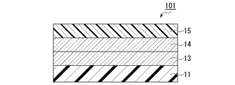
- FIG. 1 is a cross-sectional view for explaining an example of the optical laminate of the present embodiment.
- the optical laminate 101 of the present embodiment is formed by laminating a transparent base material 11, an adhesion layer 13, an optical functional layer 14, and an antifouling layer 15 in this order.
- the adhesion layer 13 is a layer that develops adhesion.
- the optical function layer 14 is a layer that expresses an optical function.
- the optical function is a function of controlling reflection, transmission, and refraction, which are the properties of light, and examples thereof include an antireflection function, a selective reflection function, an antiglare function, and a lens function.
- the optical functional layer 14 is preferably any one selected from an antireflection layer, a selective reflection layer and an antiglare layer.
- Known antireflection layers, selective reflection layers, and antiglare layers can be used.
- the antireflection layer, the selective reflection layer, and the antiglare layer may all be a single layer, or may be a laminated body of a plurality of layers.
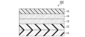
- FIG. 2 is a cross-sectional view showing another example of the optical laminate of the present embodiment.
- the optical laminate 102 shown in FIG. 2 is formed by laminating a transparent base material 11, a hard coat layer 12, an adhesion layer 13, an optical functional layer 14, and an antifouling layer 15 in this order.
- the adhesion layer 13 is a layer that develops adhesion.
- the optical function layer 14 is a layer that expresses an optical function.
- the optical function is a function of controlling reflection, transmission, and refraction, which are the properties of light, and examples thereof include an antireflection function, a selective reflection function, an antiglare function, and a lens function.
- the optical functional layer 14 is preferably any one selected from an antireflection layer, a selective reflection layer and an antiglare layer.
- Known antireflection layers, selective reflection layers, and antiglare layers can be used.
- the antireflection layer, the selective reflection layer, and the antiglare layer may all be a single layer, or may be a laminated body of a plurality of layers.
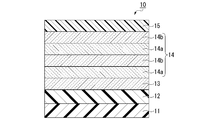
- FIG. 3 is a cross-sectional view showing another example of the optical laminate of the present embodiment.
- the optical laminate 101 shown in FIG. 3 is provided with an antireflection layer as the optical functional layer 14 in the optical laminate 102 shown in FIG.
- the optical functional layer 14 (antireflection layer) is composed of a laminated body in which low refractive index layers 14b and high refractive index layers 14a are alternately laminated.
- the optical functional layer 14 shown in FIG. 2 has a hard coat layer 12, an adhesion layer 13, a high refractive index layer 14a, a low refractive index layer 14b, a high refractive index layer 14a, and a low refractive index layer 14b in this order from the transparent substrate 11 side.
- the antifouling layer 15 is laminated in this order. Therefore, the antifouling layer 15 is in contact with the low refractive index layer 14b of the optical functional layer 14.
- the transparent base material 11 may be formed of a transparent material capable of transmitting light in the visible light region, and for example, a plastic film is preferably used.
- a plastic film is preferably used.
- the constituent materials of the plastic film include polyester resin, acetate resin, polyether sulfone resin, polycarbonate resin, polyamide resin, polyimide resin, polyolefin resin, (meth) acrylic resin, and polychloride.
- the "transparent material” as used in the present invention means a material having a light transmittance of 80% or more in the wavelength range used, as long as the effect of the present invention is not impaired.
- (meth) acrylic means methacryl and acrylic.
- the transparent base material 11 may contain a reinforcing material as long as the optical properties are not significantly impaired, and examples thereof include cellulose nanofibers and nanosilica.
- a reinforcing material such as cellulose nanofibers and nanosilica.
- polyester-based resins, acetate-based resins, polycarbonate-based resins, and polyolefin-based resins are preferably used.
- a triacetyl cellulose (TAC) base material is preferably used.
- a glass film can also be used as an inorganic base material.
- the plastic film is a TAC base material
- the hard coat layer 12 is formed on one surface side thereof, a permeation layer is formed in which a part of the components constituting the hard coat layer 12 permeates.
- the adhesion between the transparent base material 11 and the hard coat layer 12 is improved, and the occurrence of interference fringes due to the difference in refractive index between the layers can be suppressed.
- the transparent base material 11 may be a film to which an optical function and / or a physical function is imparted.
- films having optical and / or physical functions include polarizing plates, retardation compensation films, heat ray blocking films, transparent conductive films, brightness improving films, barrier property improving films, and the like.
- the thickness of the transparent base material 11 is not particularly limited, but is preferably 25 ⁇ m or more, for example.
- the film thickness of the transparent base material 11 is more preferably 40 ⁇ m or more.
- the thickness of the transparent base material 11 is 25 ⁇ m or more, the rigidity of the base material itself is ensured, and wrinkles are less likely to occur even if stress is applied to the optical laminate 10.
- the thickness of the transparent base material 11 is 25 ⁇ m or more, even if the hard coat layer 12 is continuously formed on the transparent base material 11, wrinkles are less likely to occur and there is less concern in manufacturing, which is preferable.
- the thickness of the transparent base material 11 is 40 ⁇ m or more, wrinkles are less likely to occur, which is preferable.
- the thickness of the transparent base material 11 is preferably 1,000 ⁇ m or less, and more preferably 600 ⁇ m or less.
- the thickness of the transparent base material 11 is 1000 ⁇ m or less, it is easy to wind the optical laminate 10 in the middle of production and the optical laminate 10 after production in a roll shape, and the optical laminate 10 can be efficiently manufactured.
- the optical laminate 10 can be made thinner and lighter.
- the thickness of the transparent base material 11 is 600 ⁇ m or less, the optical laminate 10 can be manufactured more efficiently, and the thin film and weight can be further reduced, which is preferable.
- the surface of the transparent base material 11 may be subjected to etching treatment such as sputtering, corona discharge, ultraviolet irradiation, electron beam irradiation, chemical conversion, oxidation, and / or undercoating treatment in advance. By performing these treatments in advance, the adhesion to the hard coat layer 12 formed on the transparent base material 11 can be improved. Further, before forming the hard coat layer 12 on the transparent base material 11, the surface of the transparent base material 11 is subjected to solvent cleaning, ultrasonic cleaning, or the like, if necessary, so that the surface of the transparent base material 11 can be cleaned. It is also preferable to remove and clean the dust.
- etching treatment such as sputtering, corona discharge, ultraviolet irradiation, electron beam irradiation, chemical conversion, oxidation, and / or undercoating treatment in advance.
- the hard coat layer 12 may be made of only a binder resin, or may contain a filler together with the binder resin as long as the transparency is not impaired.
- the filler one made of an organic substance may be used, one made of an inorganic substance may be used, or one made of an organic substance and an inorganic substance may be used.
- the binder resin used for the hard coat layer 12 is preferably a transparent resin, and for example, an ionizing radiation curable resin, a thermoplastic resin, a thermosetting resin, etc., which are resins that are cured by ultraviolet rays or electron beams, may be used. can.
- Examples of the ionizing radiation curable resin used for the binder resin of the hard coat layer 12 include ethyl (meth) acrylate, ethylhexyl (meth) acrylate, styrene, methylstyrene, N-vinylpyrrolidone and the like.
- Examples of the compound which is an ionizing radiation curable resin having two or more unsaturated bonds include trimethylpropantri (meth) acrylate, tripropylene glycol di (meth) acrylate, diethylene glycol di (meth) acrylate, and dipropylene.
- Glycoldi (meth) acrylate pentaerythritol tri (meth) acrylate, pentaerythritol tetra (meth) acrylate, dipentaerythritol hexa (meth) acrylate, 1,6-hexanediol di (meth) acrylate, neopentyl glycol di (meth) ) Acrylate, Trimethylol Propanetri (meth) Acrylate, Ditrimethylol Propanetetra (Meta) Acrylate, Dipentaerythritol Penta (Meta) Acrylate, Tripentaerythritol Octa (Meta) Acrylate, Tetrapentaerythritol Deca (Meta) Acrylate, Isocyanuric Acid Tri (meth) acrylate, di (meth) isocyanurate acrylate, polyester tri (meth) acrylate, polyester di (meth) acrylate
- pentaerythritol triacrylate PETA
- dipentaerythritol hexaacrylate DPHA
- pentaerythritol tetraacrylate PETA
- (meth) acrylate refers to methacrylate and acrylate.
- a resin obtained by modifying the above-mentioned compound with PO (propylene oxide), EO (ethylene oxide), CL (caprolactone) or the like can also be used as the ionizing radiation curable resin.
- thermoplastic resin used for the binder resin of the hard coat layer 12 examples include a styrene resin, a (meth) acrylic resin, a vinyl acetate resin, a vinyl ether resin, a halogen-containing resin, an alicyclic olefin resin, and a polycarbonate resin.
- examples thereof include resins, polyester resins, polyamide resins, cellulose derivatives, silicone resins and rubbers or elastomers.
- the thermoplastic resin is preferably amorphous and soluble in an organic solvent (particularly a common solvent capable of dissolving a plurality of polymers and curable compounds).
- styrene resins (meth) acrylic resins, alicyclic olefin resins, polyester resins, cellulose derivatives (cellulose esters, etc.) and the like are preferable.
- thermosetting resin used for the binder resin of the hard coat layer 12 examples include phenol resin, urea resin, diallyl phthalate resin, melamine resin, guanamine resin, unsaturated polyester resin, polyurethane resin, epoxy resin, aminoalkyd resin, and melamine.
- phenol resin urea resin
- diallyl phthalate resin diallyl phthalate resin
- melamine resin guanamine resin
- unsaturated polyester resin polyurethane resin
- epoxy resin epoxy resin
- aminoalkyd resin aminoalkyd resin
- melamine examples of the thermosetting resin used for the binder resin of the hard coat layer 12
- -Urea cocondensate resin silicon resin
- polysiloxane resin including so-called silsesquioxane such as cage and ladder
- the hard coat layer 12 may contain an organic resin and an inorganic material, or may be an organic-inorganic hybrid material.
- the one formed by the sol-gel method can be mentioned.
- the inorganic material include silica, alumina, zirconia, and titania.
- the organic material include acrylic resin.
- Various fillers contained in the hard coat layer 12 can be selected depending on the use of the optical laminate 10 from the viewpoints of antiglare property, adhesion to the optical functional layer 14 described later, and anti-blocking property. Specifically, for example, known particles such as silica (Si oxide) particles, alumina (aluminum oxide) particles, and organic fine particles can be used.
- the hard coat layer 12 may contain, for example, a binder resin and silica particles and / or alumina particles as a filler. By dispersing silica particles and / or alumina particles as a filler in the hard coat layer 12, fine irregularities can be formed on the surface of the hard coat layer 12. These silica particles and / or alumina particles may be exposed on the surface of the hard coat layer 12 on the optical functional layer 14 side. In this case, the binder resin of the hard coat layer 12 and the optical functional layer 14 are strongly bonded. Therefore, the adhesion between the hard coat layer 12 and the optical functional layer 14 is improved, the hardness of the hard coat layer 12 is increased, and the scratch resistance of the optical laminate 10 is improved.
- the average particle size of the silica particles and / or the alumina particles as the filler of the hard coat layer 12 is, for example, 800 nm or less, preferably 780 nm or less, and more preferably 100 nm or less.
- organic fine particles can be used as the filler contained in the hard coat layer 12.
- the organic fine particles include acrylic resin.
- the particle size of the organic fine particles is preferably 10 ⁇ m or less, more preferably 5 ⁇ m or less, and particularly preferably 3 ⁇ m or less.
- various reinforcing materials can be used in order to impart toughness to the hard coat layer 12 as long as the optical characteristics are not impaired.
- the reinforcing material include cellulose nanofibers.
- the thickness of the hard coat layer 12 is not particularly limited, but is preferably 0.5 ⁇ m or more, more preferably 1 ⁇ m or more, for example.
- the thickness of the hard coat layer 12 is preferably 100 ⁇ m or less.
- the thickness of the hard coat layer 12 is 0.5 ⁇ m or more, sufficient hardness can be obtained, so that scratches in manufacturing are less likely to occur.
- the optical laminate 10 can be made thinner and lighter.
- the thickness of the hard coat layer 12 is 100 ⁇ m or less, microcracks of the hard coat layer 12 generated when the optical laminate 10 in the process of manufacturing is bent are less likely to occur, and the productivity is improved.
- the hard coat layer 12 may be a single layer or may be a stack of a plurality of layers. Further, the hard coat layer 12 may be further provided with known functions such as an ultraviolet absorption performance, an antistatic performance, a refractive index adjusting function, and a hardness adjusting function. Further, the function imparted to the hard coat layer 12 may be imparted in a single hard coat layer, or may be imparted by being divided into a plurality of layers.
- the adhesion layer 13 is a layer formed to improve the adhesion between the transparent base material 11 or the hard coat layer 12 which is an organic film and the optical functional layer 14 which is an inorganic film.
- an adhesion layer 13 is provided between the hard coat layer 12 and the optical functional layer 14.
- the adhesion layer 13 has a function of bringing the hard coat layer 12 and the optical functional layer 14 into close contact with each other.
- the adhesion layer 13 is preferably made of an oxygen-deficient metal oxide or metal.
- the oxygen-deficient metal oxide refers to a metal oxide in which the number of oxygen is insufficient compared to the stoichiometric composition.
- oxygen-deficient metal oxide examples include SiOx, ALOx, TiOx, ZrOx, CeOx, MgOx, ZnOx, TaOx, SbOx, SnOx, and MnOx.
- the metal examples include Si, Al, Ti, Zr, Ce, Mg, Zn, Ta, Sb, Sn, Mn, and In.
- the close contact layer 13 may have, for example, a layer in which x in SiOx is more than 0 and less than 2.0.
- the adhesion layer may be formed of a mixture of a plurality of types of metals or metal oxides.
- the thickness of the adhesion layer is preferably more than 0 nm and 20 nm or less, and particularly preferably 1 nm or more and 10 nm or less, from the viewpoint of maintaining transparency and adhesion to the optical functional layer and obtaining good optical characteristics.
- the optical functional layer 14 is a laminated body that exhibits an antireflection function.
- the optical functional layer 14 shown in FIG. 3 is a laminated body of a total of four layers in which the high refractive index layer 14a and the low refractive index layer 14b are alternately laminated in order from the close contact layer 13 side.
- the number of layers of the high refractive index layer 14a and the low refractive index layer 14b is not particularly limited, and the number of layers of the high refractive index layer 14a and the low refractive index layer 14b can be any number.
- the optical functional layer 14 is composed of a laminated body in which the low refractive index layer 14b and the high refractive index layer 14a are alternately laminated, it is incident from the antifouling layer 15 side.
- the light is diffused by the optical functional layer 14. Therefore, an antireflection function for preventing the light incident from the antifouling layer 15 side from being reflected in one direction can be obtained.
- the low refractive index layer 14b preferably contains an oxide of Si from the viewpoint of easy availability and cost, and is preferably a layer containing SiO 2 (oxide of Si) or the like as a main component.
- the SiO 2 monolayer film is colorless and transparent.
- the main component of the low refractive index layer 14b means a component contained in the low refractive index layer 14b in an amount of 50% by mass or more.
- the low refractive index layer 14b is a layer containing an oxide of Si as a main component, it may contain another element of less than 50% by mass.
- the content of an element other than the oxide of Si is preferably 10% or less.
- Na may be contained for the purpose of improving durability, Zr and Al for the purpose of improving hardness, N, and Zr and Al for the purpose of improving alkali resistance.
- the refractive index of the low refractive index layer 14b is preferably 1.20 to 1.60, and more preferably 1.30 to 1.50.
- Examples of the dielectric used for the low refractive index layer 14b include magnesium fluoride (MgF 2 , refractive index 1.38) and the like.
- the refractive index of the high refractive index layer 14a is preferably 2.00 to 2.60, and more preferably 2.10 to 2.45.
- Examples of the dielectric used for the high refractive index layer 14a include niobide pentoxide (Nb 2 O 5 , refractive index 2.33), titanium oxide (TiO 2 , refractive index 2.33 to 2.55), and tungsten oxide (WO).
- Refractive index 2.2 Celium oxide (CeO 2 , Refractive index 2.2), Tantalum pentoxide (Ta 2 O 5 , Refractive index 2.16), Zinc oxide (ZnO, Refractive index 2.1), Examples thereof include indium tin oxide (ITO, refractive index 2.06) and zirconium oxide (ZrO 2 , refractive index 2.2).
- ITO indium tin oxide
- IZO indium zinc oxide
- the optical functional layer 14 for example, it is preferable to use a high refractive index layer 14a made of niobium pentoxide (Nb 2 O 5 , refractive index 2.33) and a low refractive index layer 14b made of SiO 2. ..
- the film thickness of the low refractive index layer 14b may be in the range of 1 nm or more and 200 nm or less, and is appropriately selected according to the wavelength range in which the antireflection function is required.
- the film thickness of the high refractive index layer 14a may be, for example, 1 nm or more and 200 nm or less, and is appropriately selected depending on the wavelength range in which the antireflection function is required.
- the film thicknesses of the high refractive index layer 14a and the low refractive index layer 14b can be appropriately selected according to the design of the optical functional layer 14, respectively.
- the high refractive index layer 14a of 5 to 50 nm, the low refractive index layer 14b of 10 to 80 nm, the high refractive index layer 14a of 20 to 200 nm, and the low refractive index layer 14b of 50 to 200 nm are used in this order from the close contact layer 13 side. be able to.
- the low refractive index layer 14b is arranged on the antifouling layer 15 side.
- the antireflection performance of the optical functional layer 14 is improved, which is preferable.
- the antifouling layer 15 is formed on the outermost surface of the optical functional layer 14 to prevent the optical functional layer 14 from being soiled. Further, when the antifouling layer 15 is applied to a touch panel or the like, the wear resistance of the optical functional layer 14 is suppressed.
- the antifouling layer 15 of the present embodiment is made of a vapor-deposited film on which an antifouling material is vapor-deposited.
- the antifouling layer 15 is formed by vacuum-depositing a fluorine-based organic compound as an antifouling material on one surface of the low refractive index layer 14b constituting the optical functional layer 14. In the present embodiment, since the antifouling material contains a fluorine-based organic compound, the optical laminate 10 has even better abrasion resistance and alkali resistance.
- a compound composed of a fluorine-modified organic group and a reactive silyl group for example, alkoxysilane
- examples of commercially available products include Optool DSX (manufactured by Daikin Corporation) and KY-100 series (manufactured by Shin-Etsu Chemical Co., Ltd.).
- the fluorine-based organic compound constituting the antifouling layer 15 a compound composed of a fluorine-modified organic group and a reactive silyl group (for example, alkoxysilane) is used as the fluorine-based organic compound, and the optical contact with the antifouling layer 15 is optical.
- a low refractive index layer 14b of the functional layer 14 a case of using one made of SiO 2, siloxane bonds are formed between the silanol group and SiO 2 and a skeleton of the fluorine-based organic compound. Therefore, the adhesion between the optical functional layer 14 and the antifouling layer 15 is good, which is preferable.
- the optical thickness of the antifouling layer 15 may be in the range of 1 nm or more and 20 nm or less, preferably 3 nm or more and 10 nm or less.
- the thickness of the antifouling layer 15 is 1 nm or more, sufficient wear resistance can be ensured when the optical laminate 10 is applied to a touch panel application or the like. Further, when the thickness of the antifouling layer 15 is 20 nm or less, the time required for vapor deposition is short, and efficient production can be performed.
- the surface roughness Ra of the antifouling layer 15 varies depending on the use and configuration of the optical laminate, but for example, in the case of a transparent antireflection layer having no antiglare function, it is preferably 3 nm or more.
- the upper limit is not particularly limited, but is preferably 9 nm or less from the viewpoint of scratch resistance, for example.
- the antifouling layer 15 includes a light stabilizer, an ultraviolet absorber, a colorant, an antistatic agent, a lubricant, a leveling agent, an antifoaming agent, an antioxidant, a flame retardant, an infrared absorber, a surfactant and the like, if necessary. May contain the additive of.
- the antifouling layer 15 formed by thin film deposition is firmly bonded to the optical functional layer 14 and has few voids and is dense. As a result, the antifouling layer 15 of the present embodiment exhibits characteristics different from those of the antifouling layer formed by a conventional method such as application of an antifouling material.
- the antifouling layer 15 of the optical laminate 10 of the present embodiment has the following characteristics. (1) The contact angle difference with respect to water after the scratch resistance test by horizontally reciprocating steel wool 500 times is 10 ° or less. (2) The contact angle with water after the scratch resistance test by horizontally reciprocating steel wool 500 times is 110 ° or more.
- L0 * , a0 * , and b0 * are the values before the scratch resistance test, and L1 * , a1 * , and b1 * are the values after the scratch resistance test.
- L0 * , a0 * , and b0 * are the values before the scratch resistance test, and L1 * , a1 * , and b1 * are the values after the scratch resistance test.
- the fluorine residual rate measured by fluorescent X-ray analysis (XRF) after immersion in a NaOH solution (liquid temperature 55 ° C.) having a concentration of 0.1 mol / L for 4 hours is 70% or more.
- the optical laminate 10 provided with the antifouling layer 15 of the present embodiment formed by vapor deposition has fewer voids and is densely formed as compared with the antifouling layer formed by coating. Further, in the optical laminate 10 of the present embodiment, the antifouling layer 15 is firmly bonded to the low refractive index layer 14b in contact with the antifouling layer 15. Therefore, the optical laminate 10 of the present embodiment has excellent visible light transmission, can maintain high abrasion resistance against repeated friction, and can maintain high resistance to alkali resistance.
- the optical laminate 10 of the present embodiment shown in FIG. 3 can be manufactured, for example, by the method shown below.
- the case where the optical laminate 10 is manufactured using the transparent base material 11 wound in a roll shape will be described as an example.
- the transparent base material 11 wound in a roll shape is unwound.
- a slurry containing the material to be the hard coat layer 12 is applied onto the transparent base material 11 by a known method, and the slurry is cured by a known method corresponding to the material to be the hard coat layer 12.
- the hard coat layer 12 is formed (hard coat layer forming step).
- the transparent base material 11 having the hard coat layer 12 formed on the surface thereof is wound into a roll by a known method.
- an adhesive layer forming step of forming the adhesive layer 13 and an optical functional layer forming step of forming the optical functional layer 14 are performed on the hard coat layer 12.
- an antifouling layer forming step of forming the antifouling layer 15 on the optical functional layer 14 is performed.
- the first surface treatment step, the adhesion layer forming step, the optical functional layer forming step, the second surface treatment step, and the antifouling layer forming step are in the process of being manufactured. It is preferable to carry out continuously while maintaining the state under reduced pressure.
- the first surface treatment step, the adhesion layer forming step, the optical functional layer forming step, the second surface treatment step, and the antifouling layer forming step are continuously performed while maintaining the optical laminate in the process of being manufactured under reduced pressure.
- a sputtering apparatus an apparatus provided with the thin film forming apparatus described in Patent Document 4 can be used.
- the manufacturing apparatus 20 shown in FIG. 4 includes a roll unwinding apparatus 4, a pretreatment apparatus 2A, a sputtering apparatus 1, a pretreatment apparatus 2B, a vapor deposition apparatus 3, and a roll winding apparatus 5. As shown in FIG. 4, these devices 4, 2A, 1, 2B, 3, and 5 are connected in this order.
- the manufacturing apparatus 20 shown in FIG. 4 unwinds the base material from the roll and continuously passes the connected apparatus (in FIG. 4, the pretreatment apparatus 2A, the sputtering apparatus 1, the pretreatment apparatus 2B, and the vapor deposition apparatus 3).
- This is a roll-to-roll type manufacturing apparatus that continuously forms a plurality of layers on a base material by winding it afterwards.
- the transport speed (line speed) of the optical laminate 10 in the middle of manufacturing can be appropriately set.
- the transport speed is preferably, for example, 0.5 to 20 m / min, and more preferably 0.5 to 10 m / min.
- the roll unwinding device 4 shown in FIG. 4 includes a chamber 34 having a predetermined depressurized atmosphere inside, and one or more vacuum pumps 21 (in FIG. 4 in FIG. 4) that discharge gas in the chamber 34 to create a decompressed atmosphere. It has one) and an unwinding roll 23 and a guide roll 22 installed in the chamber 34. As shown in FIG. 4, the chamber 34 is connected to the chamber 31 of the sputtering apparatus 1. A transparent base material 11 having a hard coat layer 12 formed on its surface is wound around the unwinding roll 23. The unwinding roll 23 supplies the transparent base material 11 having the hard coat layer 12 formed on its surface to the pretreatment device 2A at a predetermined transport speed.
- the pretreatment device 2A shown in FIG. 4 includes a chamber 32 having a predetermined decompression atmosphere inside, a can roll 26, a plurality of guide rolls 22 (two in FIG. 4), and a plasma discharge device 42. As shown in FIG. 4, the can roll 26, the guide roll 22, and the plasma discharge device 42 are installed in the chamber 32. As shown in FIG. 4, the chamber 32 is connected to the chamber 31 of the sputtering apparatus 1.
- the can roll 26 and the guide roll 22 conveyed the transparent base material 11 on which the hard coat layer 12 was formed, which was sent from the roll unwinding device 4, at a predetermined transfer speed, and the surface of the hard coat layer 12 was treated.
- the transparent base material 11 is sent to the sputtering apparatus 1.
- the plasma discharge device 42 is arranged so as to face the outer peripheral surface of the can roll 26 at a predetermined interval.
- the plasma discharge device 42 ionizes the gas by glow discharge.
- the gas is preferably inexpensive, inert and does not affect the optical characteristics, and for example, argon gas, oxygen gas, nitrogen gas, helium gas and the like can be used.
- the gas it is preferable to use argon gas because it has a large mass, is chemically stable, and is easily available.
- the sputtering apparatus 1 shown in FIG. 4 includes a chamber 31 having a predetermined depressurized atmosphere inside, and one or a plurality of vacuum pumps 21 (two in FIG. 4) that discharge gas in the chamber 31 to create a depressurized atmosphere. ), A plurality of (two in FIG. 4) guide rolls 22, and a plurality of (four in the example shown in FIG. 4) film forming portions 41. As shown in FIG. 4, the film forming roll 25, the guide roll 22, and the film forming section 41 are installed in the chamber 31. As shown in FIG. 4, the chamber 31 is connected to the chamber 32 of the pretreatment device 2B.
- the film forming roll 25 and the guide roll 22 convey the transparent base material 11 on which the surface-treated hard coat layer 12 is formed, which is sent from the pretreatment apparatus 2A, at a predetermined transfer speed, and are transferred onto the hard coat layer 12.
- the transparent base material 11 on which the adhesion layer 13 and the optical functional layer 14 are formed is supplied to the pretreatment device 2B.
- the adhesion layer 13 is laminated by sputtering on the hard coat layer 12 of the transparent base material 11 running on the film forming roll 25, and the high refractive index layer 14a and the low refractive index are placed on the adhesion layer 13 by sputtering.
- the layers 14b are alternately laminated to form the optical functional layer 14.
- a plurality of film forming portions 41 are arranged so as to face the outer peripheral surface of the film forming roll 25 at a predetermined interval and are provided so as to surround the film forming roll 25.
- the number of film-forming portions 41 is determined according to the total number of layers of the adhesion layer 13, the high-refractive index layer 14a forming the optical functional layer 14, and the low-refractive index layer 14b. When it is difficult to secure the distance between the adjacent film forming portions 41 due to the large total number of layers of the high refractive index layer 14a and the low refractive index layer 14b forming the adhesion layer 13 and the optical functional layer 14.
- a plurality of film forming rolls 25 may be provided in the chamber 31, and a film forming section 41 may be arranged around each film forming roll 25.
- a guide roll 22 may be further provided if necessary.
- a plurality of chambers 31 provided with the film forming roll 25 and the film forming portion 41 may be connected. Further, the diameter of the film forming roll 25 may be appropriately changed in order to easily secure the distance between the adjacent film forming portions 41.
- a predetermined target (not shown) is installed in each film forming section 41.
- a voltage is applied to the target by a known structure.
- a gas supply unit (not shown) that supplies a predetermined reactive gas and a carrier gas to the target at a predetermined flow rate in the vicinity of the target, and a known magnetic field generation source that forms a magnetic field on the surface of the target (not shown). (Not shown) is provided.
- the target material and the type and flow rate of the reactive gas are the adhesion layer 13, the high refractive index layer 14a, which are formed on the transparent base material 11 by passing between the film forming portion 41 and the film forming roll 25. It is appropriately determined according to the composition of the low refractive index layer 14b. For example, when forming a layer made of SiO 2 , Si is used as a target and O 2 is used as a reactive gas. Further, for example, when forming a layer composed of Nb 2 O 5 , Nb is used as a target and O 2 is used as a reactive gas.
- the magnetron sputtering method is not limited to the magnetron sputtering method, and a two-pole sputtering method using plasma generated by DC glow discharge or high frequency, a three-pole sputtering method in which a hot cathode is added, or the like may be used. ..
- the sputtering apparatus 1 includes an optical monitor (not shown) as a measuring unit for measuring optical characteristics after forming the layers to be the adhesion layer 13 and the optical functional layer 14. Thereby, the quality of the formed adhesion layer 13 and the optical functional layer 14 can be confirmed.
- an optical monitor not shown
- Examples of the optical monitor include those that measure the optical characteristics in the width direction of the adhesion layer 13 and the optical functional layer 14 formed on the hard coat layer 12 by an optical head capable of scanning in the width direction. Be done.
- an optical monitor for example, by measuring the peak wavelength of reflectance as an optical characteristic and converting it into an optical thickness, the optical thickness distribution in the width direction of the adhesion layer 13 and the optical functional layer 14 can be obtained. Can be measured.
- By measuring the optical characteristics using an optical monitor it is possible to form an optical laminate 10 having an adhesion layer 13 and an optical functional layer 14 having optimum optical characteristics while adjusting the sputtering conditions in real time.
- the pretreatment device 2B shown in FIG. 4 includes a chamber 32 having a predetermined decompression atmosphere inside, a can roll 26, a plurality of guide rolls 22 (two in FIG. 4), and a plasma discharge device 42. As shown in FIG. 4, the can roll 26, the guide roll 22, and the plasma discharge device 42 are installed in the chamber 32. As shown in FIG. 4, the chamber 32 is connected to the chamber 33 of the vapor deposition apparatus 3.
- the can roll 26 and the guide roll 22 convey the transparent base material 11 on which each layer is formed up to the optical functional layer 14 sent from the sputtering apparatus 1 at a predetermined conveying speed, and the surface of the optical functional layer 14 is treated.
- the transparent base material 11 is sent to the vapor deposition apparatus 3.
- the plasma discharge device 42 for example, the same one as the pretreatment device 2A can be used.
- the thin-film deposition apparatus 3 shown in FIG. 4 includes a chamber 33 having a predetermined depressurized atmosphere inside, and one or a plurality of vacuum pumps 21 (one in FIG. 4) for discharging the gas in the chamber 33 to create a depressurized atmosphere. ), A plurality of guide rolls 22 (four in FIG. 4), a vapor deposition source 43, and a heating device 53. As shown in FIG. 4, the guide roll 22 and the vapor deposition source 43 are installed in the chamber 33.
- the chamber 33 is connected to the chamber 35 of the roll winding device 5.
- the thin-film deposition source 43 is arranged so as to face the transparent base material 11 whose surface of the optical functional layer 14 has been treated, which is conveyed substantially horizontally between two adjacent guide rolls 22.
- the thin-film deposition source 43 supplies an evaporative gas made of a material to be the antifouling layer 15 onto the optical functional layer 14.
- the orientation of the vapor deposition source 43 can be set arbitrarily.
- the heating device 53 heats the material to be the antifouling layer 15 to a vapor pressure temperature.
- the heating device 53 one that heats by a resistance heating method, a heater heating method, an induction heating method, an electron beam method, or the like can be used.
- a container containing an antifouling material to be the antifouling layer 15 is used as a resistor to energize and heat the container.
- the container is heated by a heater arranged on the outer circumference of the container.
- the container or antifouling material is heated by an electromagnetic induction action from an induction coil installed outside.
- the thin-film deposition apparatus 3 shown in FIG. 4 has a guide plate (not shown) that guides the vapor-deposited material evaporated by the vapor deposition source 43 to a predetermined position, and a film thickness meter (not shown) for observing the thickness of the antifouling layer 15 formed by the vapor deposition. It includes a vacuum pressure gauge (not shown) for measuring the pressure in the chamber 33 (not shown), and a power supply device (not shown).
- the guide plate may have any shape as long as the evaporated vaporized material can be guided to a desired position. The guide plate may not be provided if it is not necessary.
- the vacuum pressure gauge for example, an ion gauge or the like can be used.
- the power supply device include a high frequency power supply.
- the roll winding device 5 shown in FIG. 4 has a chamber 35 having a predetermined depressurized atmosphere inside, and one or more vacuum pumps 21 (in FIG. 4 in FIG. 4) that discharge gas in the chamber 35 to create a decompressed atmosphere.
- a transparent base material 11 (optical laminate 10) on which each layer up to the antifouling layer 15 is formed is wound around the winding roll 24.
- the take-up roll 24 and the guide roll 22 take up the optical laminate 10 at a predetermined take-up speed. If necessary, a carrier film may also be used.
- the vacuum pump 21 provided in the manufacturing apparatus 20 shown in FIG. 4 for example, a dry pump, an oil rotary pump, a turbo molecular pump, an oil diffusion pump, a cryopump, a sputter ion pump, a getter pump and the like can be used. ..
- the vacuum pump 21 can be appropriately selected or used in combination in each of the chambers 31, 32, 33, 34 and 35 to create a desired depressurized state.
- the vacuum pump 21 only needs to be able to maintain both the chamber 31 of the sputtering apparatus 1 and the chamber 33 of the vapor deposition apparatus 3 in a desired depressurized state, and the installation position and number of the vacuum pumps 21 in the manufacturing apparatus 20 are not particularly limited. Further, in the manufacturing apparatus 20 shown in FIG. 4, the roll unwinding apparatus 4, the pretreatment apparatus 2A, the sputtering apparatus 1, the pretreatment apparatus 2B, the vapor deposition apparatus 3, and the roll winding apparatus 5 are connected to each other. Therefore, the vacuum pump 21 may be installed in the chambers 31, 32, 33, 34, and 35, respectively, and both the chamber 31 of the sputtering apparatus 1 and the chamber 33 of the vapor deposition apparatus 3 are maintained in a desired depressurized state. If possible, it may be installed in only some of the chambers 31, 32, 33, 34, and 35.
- the first surface treatment step, the adhesion layer forming step, the optical functional layer forming step, the second surface treatment step, and the antifouling layer forming step are performed on the optical laminate during manufacturing.
- a method of continuously performing 10 while maintaining the state under reduced pressure will be described.
- the unwinding roll 23 around which the transparent base material 11 having the hard coat layer 12 formed on the surface is wound is installed in the chamber 34 of the roll unwinding device 4.
- the unwinding roll 23 and the guide roll 22 are rotated to feed the transparent base material 11 having the hard coat layer 12 formed on the surface to the pretreatment device 2A at a predetermined transport speed.
- a first surface treatment step is performed as a pretreatment for the surfaces on which the adhesion layer 13 and the optical functional layer 14 are formed.
- the first surface treatment step is performed on the transparent base material 11 on which the hard coat layer 12 is formed.
- the can roll 26 and the guide roll 22 are rotated to carry the transparent base material 11 on which the hard coat layer 12 is formed at a predetermined transport speed, and the hard roll 26 travels on the can roll 26.
- the surface of the coat layer 12 is treated.
- glow discharge treatment for example, glow discharge treatment, plasma treatment, ion etching, alkali treatment and the like can be used. Among these, it is preferable to use glow discharge treatment because large area treatment is possible.
- the glow discharge treatment can be performed, for example, with a treatment strength of 0.1 to 10 kwh.
- the surface of the hard coat layer 12 is roughened at the nano level, and substances having a weak bonding force existing on the surface of the hard coat layer 12 are present. Will be removed. As a result, the adhesion between the hard coat layer 12 and the optical functional layer 14 formed on the hard coat layer 12 is improved.
- the adhesion layer forming step and the optical functional layer forming step are performed in the chamber 31 of the sputtering apparatus 1. Specifically, the hard filming roll 25 and the guide roll 22 are rotated to carry the transparent base material 11 on which the hard coat layer 12 is formed at a predetermined transfer speed, and the hard film runs on the film forming roll 25. The adhesion layer 13 and the optical functional layer 14 are formed on the coat layer 12.
- the adhesion layer 13 is formed by sputtering by changing the type and flow rate of the target material installed in each film forming section 41 or the reactive gas supplied from the gas supply section, and the adhesion layer 13 is formed on the target material.
- the high refractive index layer 14a and the low refractive index layer 14b are alternately laminated. That is, the adhesion layer forming step and the optical functional layer forming step are continuously performed in the sputtering apparatus 1. As a result, the adhesion layer 13 and the optical functional layer 14 which is an antireflection layer are formed.
- the adhesion layer 13 When a SiO x film is formed as the adhesion layer 13, it is preferably formed by reactive sputtering in a mixed gas atmosphere of oxygen gas and argon gas using a silicon target.
- the adhesion layer 13 When the adhesion layer 13, the high refractive index layer 14a, and the low refractive index layer 14b are continuously laminated by sputtering, the adhesion layer 13 is formed, the high refractive index layer 14a is formed, and the low refractive index layer 14b is formed.
- the target material may be changed depending on the time of film formation.
- a layer made of the target material and a layer made of an oxide of the target material are alternately formed and adhered to each other.
- the layer 13, the high refractive index layer 14a, and the low refractive index layer 14b may be used.
- the pressure during sputtering for forming the adhesion layer 13 and the optical functional layer 14 varies depending on the metal to be sputtered, but may be 2 Pa or less, preferably 1 Pa or less, and preferably 0.6 Pa or less. More preferably, it is 0.2 Pa or less, and particularly preferably 0.2 Pa or less.
- the pressure during sputtering is 1 Pa or less under reduced pressure, the mean free path of the film-forming molecules becomes long, and the film-forming molecules are laminated with high energy, resulting in a denser and better film quality.
- the transparent base material 11 on which the adhesion layer 13 and the optical functional layer 14 are formed on the hard coat layer 12 is sent out to the pretreatment apparatus 2B by the rotation of the film forming roll 25 and the guide roll 22.
- a second surface treatment step is performed as a pretreatment for the surface on which the antifouling layer 15 is formed.
- the transparent base material 11 on which the optical functional layer 14 is formed obtained by the optical functional layer forming step is continuously subjected to the second surface treatment while being maintained under reduced pressure without being exposed to the atmosphere. Perform the process.
- the can roll 26 and the guide roll 22 are rotated to transport the transparent base material 11 on which each layer up to the optical functional layer 14 is formed at a predetermined transport speed, while transporting the transparent base material 11 on the can roll 26.
- the surface of the traveling optical functional layer 14 is subjected to a discharge treatment.
- the optical functional layer 14 As a surface treatment method for the optical functional layer 14, for example, glow discharge treatment, plasma treatment, ion etching, alkali treatment and the like can be used. Among these, it is preferable to use glow discharge treatment because large area treatment is possible.
- glow discharge treatment because large area treatment is possible.
- the surface of the optical functional layer 14 is subjected to an electric discharge treatment, the surface of the optical functional layer 14 is etched and the roughness of the surface of the optical functional layer 14 changes.
- the surface roughness Ra of the optical functional layer 14 can be controlled by setting the integrated output during the discharge process within an appropriate range.
- the integrated output is a value obtained by dividing the product of the glow discharge output irradiated to the optical functional layer 14 and the irradiation time per unit area during the discharge process.
- the conditions of the discharge process can be set as appropriate. By appropriately setting the conditions of the electric discharge treatment, the adhesion between the optical functional layer 14 and the antifouling layer 15 formed on the optical functional layer 14 becomes good, and the optical laminate having even better abrasion resistance and alkali resistance. 10 is obtained.
- the surface roughness Ra of the optical functional layer 14 after the discharge treatment differs depending on the surface roughness of the hard coat layer 12 provided under the optical functional layer 14. Further, the surface roughness Ra of the optical functional layer 14 after the discharge treatment affects the surface roughness Ra of the antifouling layer 15 formed on the optical functional layer 14.
- the surface of the optical functional layer is treated so that the rate of change in surface roughness represented by the following (Equation 1) is 1 to 25%.
- Rate of change in surface roughness (%) ((Ra2 / Ra1) -1) x 100 (%) ...
- Ra1 is the optical functional layer before surface treatment.
- the surface roughness (Ra) is shown, and Ra2 shows the surface roughness (Ra) of the optical functional layer after the surface is treated.
- the second surface treatment step is preferably performed so that the rate of change in surface roughness represented by (Equation 1) is 5% to 25%, and more preferably 8% to 25%. It is more preferably 8% to 20%, further preferably 8% to 15%, and even more preferably 10% to 14%.
- the rate of change in surface roughness represented by (Equation 1) is 1% or more, the effect of improving the adhesion between the optical functional layer 14 and the antifouling layer 15 by performing the second surface treatment step becomes remarkable. ..
- the rate of change of the surface roughness represented by (Equation 1) is 25% or less, the thickness of the optical functional layer 14 is appropriate, so that an antifouling layer having a uniform thickness is placed on the optical functional layer 14. 15 is formed.
- the surface roughness Ra of the optical functional layer 14 can be measured by the method shown below. Using an atomic force microscope (AFM), the surface roughness Ra in the area of 1 ⁇ m 2 on the surface of the optical functional layer 14 is measured.
- AFM atomic force microscope
- the transparent base material 11 having the surface of the optical functional layer 14 treated is sent out to the vapor deposition apparatus 3 by the rotation of the can roll 26 and the guide roll 22.
- the antifouling layer forming step is performed in the chamber 33 of the vapor deposition apparatus 3.
- the transparent base material 11 obtained by the surface treatment of the optical functional layer 14 obtained by the second surface treatment step is continuously antifouling while being maintained under reduced pressure without being exposed to the atmosphere.
- the guide roll 22 is rotated to transport the transparent base material 11 having the surface of the optical functional layer 14 treated at a predetermined transport speed, and the vapor deposition source 43 is transferred to the surface of the optical functional layer 14. Is vapor-deposited.
- an antifouling material made of a fluorine-based organic compound to be an antifouling layer 15 is heated to a vapor pressure temperature by a heating device 53, and the obtained evaporation gas is heated from a vapor deposition source 43 under a reduced pressure environment.
- the surface is supplied and adhered to the treated optical functional layer 14, and the antifouling layer 15 is formed by vacuum evaporation.
- the pressure at which the antifouling layer 15 is vacuum-deposited is, for example, preferably 0.05 Pa or less, more preferably 0.01 Pa or less, and particularly preferably 0.001 Pa or less.
- the optical laminate 10 in which the antifouling layer 15 is formed by vacuum vapor deposition on the adhesion layer 13 and the optical functional layer 14 formed by sputtering can be obtained.
- the transparent base material 11 (optical laminate 10) on which each layer up to the antifouling layer 15 is formed is sent out to the roll winding device 5 by the rotation of the guide roll 22. Then, in the chamber 35 of the roll winding device 5, the optical laminate 10 is wound around the winding roll 24 by the rotation of the winding roll 24 and the guide roll 22.
- the optical functional layer forming step and the antifouling layer forming step are continuously performed under reduced pressure.
- the optical functional layer forming step and the prevention It is more preferable that the foul layer forming step is continuously performed in-line while maintaining the reduced pressure state.
- the in-line means that the antifouling layer forming step is performed without exposing the optical functional layer 14 formed in the optical functional layer forming step to the atmosphere.
- the optical functional layer forming step and the antifouling layer forming step under reduced pressure By continuously performing the optical functional layer forming step and the antifouling layer forming step under reduced pressure, natural oxidation is performed on the optical functional layer 14 formed in the optical functional layer forming step before the antifouling layer 15 is formed. The formation of a film is suppressed. Further, it is possible to prevent contamination such as foreign matter when winding the roll from adhering to the optical functional layer 14 and impairing the adhesion between the optical functional layer 14 and the antifouling layer 15. Therefore, after the optical functional layer forming step, the transparent base material 11 in which each layer up to the optical functional layer 14 is formed is taken out from the chamber in the reduced pressure state, and then installed again in the chamber to perform the antifouling layer forming step under reduced pressure. An optical laminate having good adhesion between the optical functional layer 14 and the antifouling layer 15 and excellent transparency can be obtained as compared with the case where the optical functional layer 14 and the antifouling layer 15 are adhered to each other.
- the antifouling layer 15 contained in the optical laminate 10 of the present embodiment is a vapor-deposited film
- higher wear resistance can be obtained as compared with, for example, an antifouling film formed by a coating method. It is presumed that this is due to the following reasons. That is, in the antifouling film formed by the coating method, voids due to the solvent contained in the paint are present. On the other hand, the vapor-deposited film does not have voids due to the solvent. Therefore, it is presumed that the vapor-deposited film has a higher density than the antifouling film formed by the coating method, and can obtain high wear resistance and alkali resistance.
- the optical functional layer 14 is formed by alternately laminating the adhesion layer forming step of forming the adhesion layer 13 and the high refractive index layer 14a and the low refractive index layer 14b.
- the optical functional layer forming step, the second surface treatment step of treating the surface of the optical functional layer 14, and the antifouling layer forming step of forming the antifouling layer 15 on the surface-treated optical functional layer 14 are included. Therefore, the adhesiveness between the optical functional layer 14 and the antifouling layer 15 formed on the optical functional layer 14 is good, and the frictional resistance and the alkali resistance are further improved.
- the surface of the optical functional layer 14 becomes It is preferable because the surface is activated by changing to an appropriate roughness and being etched, and thus the reactivity with the antifouling layer 15 formed on the optical functional layer 14 is improved.
- the optical laminate 10 can be continuously formed by the roll-to-roll method, and the film thickness can be controlled with high accuracy. Therefore, in the optical functional layer forming step, It is preferable to form the optical functional layer 14 by sputtering.
- the first surface treatment step, the optical functional layer forming step, the second surface treatment step, and the antifouling layer forming step are continuously performed while maintaining the optical laminate in the process of being manufactured under reduced pressure.
- the depressurizing conditions in the chamber may be different between the sputtering apparatus and the vapor deposition apparatus.
- the film formation result is measured with a measuring instrument over time, and the result is used as a subsequent step. It is preferable to feed back to the conditions of the manufacturing process corresponding to the above. This makes it easier to optimize the characteristics of the entire optical laminate, and the in-plane characteristics of the optical laminate can be made uniform. It is also possible to provide feedback on manufacturing conditions in the same process using a measuring instrument. In this case, the layer formed in the step has uniform and stable characteristics.
- the case where the second surface treatment step is performed between the optical functional layer forming step and the antifouling layer forming step has been described as an example, but if the second surface treatment step is performed as necessary, it may be performed. Well, you don't have to. Even when the second surface treatment step is not performed, it is preferable that the optical functional layer forming step and the antifouling layer forming step are continuously performed under reduced pressure.
- the manufacturing shown in FIG. 4 including a pretreatment device 2A, a sputtering device 1, a pretreatment device 2B, a vapor deposition device 3, a roll unwinding device 4, and a roll winding device 5 is provided.
- the case where the optical laminate 10 is continuously manufactured by the roll-to-roll method using the apparatus 20 has been described as an example, but the manufacturing apparatus for producing the optical laminate 10 is the manufacturing apparatus 20 shown in FIG. Not limited.
- a pretreatment for cleaning the surface of the optical functional layer 14 on which the antifouling layer 15 is formed is performed between the chamber 33 of the vapor deposition apparatus 3 and the chamber 32 of the pretreatment apparatus 2B.
- a chamber (not shown) may be provided.
- a post-treatment chamber (not shown) for performing the inspection may be provided.
- the manufacturing apparatus 20 shown in FIG. 4 is provided with a hard coat layer forming apparatus for forming the hard coat layer 12 on the surface of the transparent base material 11 between the roll unwinding apparatus 4 and the sputtering apparatus 1. May be good.
- a hard coat layer forming apparatus for forming the hard coat layer 12 on the surface of the transparent base material 11 between the roll unwinding apparatus 4 and the sputtering apparatus 1. May be good.
- the optical functional layer 14 and the antifouling layer 15 but also the hard coat layer 12 can be continuously manufactured by the roll-to-roll method, which is preferable.
- the optical functional layer forming step is performed using the sputtering apparatus and the antifouling layer forming step is performed using the vapor deposition apparatus has been described as an example, but the case where the second surface treatment step is not performed has been described.
- the optical functional layer forming step and the antifouling layer forming step may be performed in the same device (in one chamber).
- various layers may be provided on the surface facing the surface on which the optical functional layer of the transparent base material is formed, if necessary.
- an adhesive layer used for adhesion to other members may be provided.
- another optical film may be provided via this pressure-sensitive adhesive layer. Examples of other optical films include polarizing films, retardation compensation films, 1/2 wave plates, and films that function as 1/4 wave plates.
- the shape of the optical laminate may be a smooth shape, or may be a shape having a nano-order uneven structure that exhibits a moth-eye or antiglare function. Further, it may have a micro to millimeter-order geometric shape such as a lens or a prism.
- the shape can be formed by, for example, a combination of photolithography and etching, shape transfer, heat pressing, or the like. In the present embodiment, since the film is formed by vapor deposition or the like, even if the base material has an uneven shape, for example, the uneven shape can be maintained.
- the article of the present embodiment is provided with the above-mentioned optical laminate 10 on the display surface of the image display unit, such as a liquid crystal display panel or an organic EL display panel.
- the image display unit such as a liquid crystal display panel or an organic EL display panel.
- the article is not limited to the image display device, for example, a window glass or goggles on which the optical laminate of the present embodiment is provided on the surface, a light receiving surface of a solar cell, a smartphone screen, a personal computer display, and information input.
- Terminals tablet terminals, AR (augmented reality) devices, VR (virtual reality) devices, lightning display boards, glass table surfaces, game machines, operation support devices for aircraft and trains, navigation systems, instrument panels, optical sensor surfaces, etc. Any material may be used as long as the optical laminate 10 is applicable.
- optical laminates produced in the following Examples and Comparative Examples are examples of functions as an antireflection film, and the gist of the present invention is not limited thereto.
- a photocurable resin composition was prepared in which the content of silica particles (filler) having an average particle size of 50 nm was 28% by mass with respect to the total solid content of the resin composition (binder resin). As shown in Table 1, the resin composition was prepared by dissolving silica particles, an acrylate, a leveling agent, and a photopolymerization initiator in a solvent.
- SR610 Polyethylene glycol diacrylate, average molecular weight of polyethylene glycol chain 600
- CN968 Hexactive aliphatic urethane acrylate with polyester skeleton
- Irgacare 184 1-hydroxy-cyclohexyl-phenyl-ketone
- a roll-shaped TAC film having a thickness of 80 ⁇ m and a length of 3900 m was prepared as the transparent base material 11, and the photocurable resin composition shown in Table 1 was applied onto the TAC film with a gravure coater and cured by irradiating with light.
- the hard coat layer 12 having a thickness of 5 ⁇ m was formed.
- the adhesion layer 13, the optical functional layer 14, and the antifouling layer 15 are continuously arranged in this order on the transparent base material 11 on which the hard coat layer 12 is formed by the method shown below.
- the optical laminates (antireflection films) of Examples 1 to 5 and Comparative Example 2 were prepared.
- the manufacturing apparatus 20 shown in FIG. 4 was used as the manufacturing apparatus.
- the line speed was set to 2 m / min.
- the first surface treatment step, the adhesion layer forming step, the optical functional layer forming step, the second surface treatment step, and the antifouling layer forming step were continuously performed while maintaining the optical laminate in the process of being manufactured under reduced pressure. ..
- An adhesion layer 13 made of SiOx having a thickness of 5 nm is formed on the hard coat layer 12 after the glow discharge treatment by sputtering in a chamber having a pressure of 1.0 Pa or less, and an Nb 2 O 5 film having a thickness of 15 nm is formed on the adhesion layer.
- SiO 2 film with a thickness of 38 nm low refractive index layer
- Nb 2 O 5 film with a thickness of 30 nm high refractive index layer
- SiO 2 film with a thickness of 102 nm low refractive index layer
- ⁇ Second surface treatment process> The surface of the optical functional layer 14 was subjected to glow discharge treatment.
- Table 2 shows the integrated output of the glow discharge process.
- Table 2 shows relative values (output relative values) with the integrated output of the glow discharge process of Example 1 as 100.
- the integrated output of the glow discharge treatment was set to 326 W ⁇ min / m 2 .
- Ra1 is the optical functional layer before surface treatment.
- the surface roughness (Ra) is shown
- Ra2 shows the surface roughness (Ra) of the optical functional layer after the surface is treated.)
- an alkoxysilane compound having a perfluoropolyether group which is an organic compound having fluorine, a vapor deposition temperature of 230 ° C., a line speed of 2.0 m / min, and a vapor deposition chamber pressure of 0.01 Pa or less on the optical functional layer 14
- An antifouling layer 15 made of KY-1901 (manufactured by Shin-Etsu Chemical Industry Co., Ltd.) was formed by thin film deposition.
- Table 2 shows the optical film thickness of the obtained antifouling layer 15. Then, the film was wound into a roll to obtain optical laminates (antireflection films) of Examples 1 to 5 and Comparative Example 2.
- Comparative Example 1 After performing the optical functional layer forming step in the same manner as in Example 1, the antifouling layer forming step was performed without performing the surface treatment step, except that the antifouling layer 15 was formed on the optical functional layer 14. In the same manner as in Example 1, the optical laminate (antireflection film) of Comparative Example 1 was produced.
- the TAC film on which the hard coat layer 12, the adhesion layer 13 and the optical functional layer 14 are formed is wound up and taken out from the manufacturing apparatus, and is of a roll-to-roll method. It was installed in the coating device (coater). Then, under atmospheric pressure, the TAC film on which the hard coat layer 12, the adhesion layer 13 and the optical functional layer 14 were formed was unwound, and the SiO 2 film of the optical functional layer 14 was unwound at a line speed of 20 m / min using a gravure coater. An antifouling agent was applied on the (low refractive index layer).
- an alkoxysilane compound having a perfluoropolyether group (KY-1901, manufactured by Shin-Etsu Chemical Industry Co., Ltd.) was used in a fluorine solvent (Fluorinert FC-3283: manufactured by 3M Japan Ltd.) at a concentration of 0. The one diluted to 1% by mass was used.
- the antifouling agent was applied so that the thickness after drying was the film thickness shown in Table 2.
- the surface roughness Ra of the antifouling layer was examined for the obtained optical laminates (antireflection films) of Examples 1 to 5 and Comparative Examples 1 to 3 by the methods shown below. The results are shown in Table 2.
- Measurement of surface roughness Ra of antifouling layer A measurement sample of 50 mm ⁇ 50 mm was cut out from the center position in the length direction and the center position in the roll width direction of each roll around which the optical laminate was wound. The surface of the sample was observed using an atomic force microscope (AFM) (trade name: SPA400, NanoNaviII; manufactured by Hitachi, Ltd.), and the surface roughness Ra in an area of 1 ⁇ m 2 was measured.
- AFM atomic force microscope
- the surface roughness Ra of the antifouling layer is affected by the surface roughness Ra of the optical functional layer below it.
- the antifouling layer formed by vapor deposition does not have voids due to the solvent contained in the paint unlike the antifouling layer formed by the coating method, and is formed at a high density.
- the effect of the surface roughness Ra of the optical functional layer underneath is greater than that of the formed antifouling layer.
- the surface of the optical functional layer is subjected to glow discharge treatment to increase the surface roughness, and the surface roughness of the antifouling layer is increased under the influence of the glow discharge treatment.
- Example 1 when the optical functional layer comes into contact with the atmosphere, a natural oxide film is formed on the optical functional layer, and the surface roughening effect due to the glow discharge treatment is reduced, whereas the optical functional layer and the antifouling layer are formed. If it is formed without contact with the atmosphere, it will not be affected. Further, the difference in surface roughness between Example 1 and Comparative Example 1 is due to the presence or absence of glow discharge treatment.
- Drop rate of each reagent 2.0 ⁇ L Measurement temperature: 25 ° C
- the contact angle after 4 seconds from the dropping of each reagent was measured at any 10 points on the surface of the test piece, and the average value was taken as the contact angle of oleic acid, n-hexadecane, and diiodomethane.
- Fluorine amount measurement test The fluorine amount (cps: count number per unit time) of the optical laminates (test pieces) of Examples 1 to 5 and Comparative Examples 1 to 3 was measured (fluorine amount before cleaning (initial state). Fluorine amount)).
- X-ray Photoelectron Spectroscopy Electrode Spectroscopic for Chemical Analysis, ESCA
- PHI5000 VersaProb * eIII manufactured by ULVAC FI Co., Ltd.
- X-ray fluorescence fluorescent X-ray fluorescence analysis method
- the ⁇ E value which is the amount of change in the * b * (based on CIE1976) value, was calculated.
- (3-2) Fluorine Residual Amount Measurement Test with Alkaline Solution In the same manner as the test in (2) above, the fluorine amount (cps) of the sample after treatment with the alkaline solution was measured using ESCA or XRF, and the sample after treatment. Fluorine residual rate (%) was calculated.
- a surface treatment step of treating the surface of the optical functional layer 14 and an antifouling layer forming step of forming the antifouling layer 15 on the surface-treated optical functional layer 14 were performed.
- the optical laminates of Examples 1 to 5 have a higher residual rate of fluorine in the alkali resistance test, a small hue change ⁇ E of 5 or less, and good alkali resistance as compared with Comparative Example 1 in which the surface treatment step was not performed. I was able to confirm that there was. Further, the optical laminates of Examples 1 to 5 have a smaller contact angle difference of 14 or less in the scratch resistance test using a waste cloth (nonwoven fabric wiper) and a residual rate of fluorine as compared with Comparative Examples 1 and 2. it was high. The optical laminates of Examples 1 to 5 had a smaller hue change in the alkali resistance test and a higher residual rate of fluorine as compared with Comparative Examples 1 and 2.
- the optical laminates of Examples 1 to 5 have a small contact angle difference of 14 or less in the scratch resistance test using a waste cloth (nonwoven fabric wiper), and the hue change in the alkali resistance test. was small, and the residual rate of fluorine was high.
Landscapes
- Chemical & Material Sciences (AREA)
- Physics & Mathematics (AREA)
- Engineering & Computer Science (AREA)
- General Physics & Mathematics (AREA)
- Optics & Photonics (AREA)
- Chemical Kinetics & Catalysis (AREA)
- Mechanical Engineering (AREA)
- Organic Chemistry (AREA)
- Materials Engineering (AREA)
- Metallurgy (AREA)
- Inorganic Chemistry (AREA)
- Thermal Sciences (AREA)
- Plasma & Fusion (AREA)
- Ceramic Engineering (AREA)
- Surface Treatment Of Optical Elements (AREA)
- Laminated Bodies (AREA)
- Surface Treatment Of Glass (AREA)
- Physical Vapour Deposition (AREA)
- Optical Elements Other Than Lenses (AREA)
Priority Applications (5)
| Application Number | Priority Date | Filing Date | Title |
|---|---|---|---|
| CN202180017403.5A CN115175806A (zh) | 2020-03-04 | 2021-03-03 | 光学层叠体的制造方法 |
| KR1020227022924A KR102745517B1 (ko) | 2020-03-04 | 2021-03-03 | 광학 적층체의 제조 방법 |
| EP21765327.8A EP4116086A4 (en) | 2020-03-04 | 2021-03-03 | METHOD FOR MANUFACTURING OPTICAL LAMINATE |
| US17/905,392 US12275226B2 (en) | 2020-03-04 | 2021-03-03 | Method of manufacturing optical laminate |
| CN202510439778.0A CN120134734A (zh) | 2020-03-04 | 2021-03-03 | 光学层叠体的制造方法 |
Applications Claiming Priority (6)
| Application Number | Priority Date | Filing Date | Title |
|---|---|---|---|
| JP2020037146 | 2020-03-04 | ||
| JP2020-037146 | 2020-03-04 | ||
| JP2020123317 | 2020-07-17 | ||
| JP2020-123317 | 2020-07-17 | ||
| JP2021032929A JP7089610B2 (ja) | 2020-03-04 | 2021-03-02 | 光学積層体の製造方法 |
| JP2021-032929 | 2021-03-02 |
Publications (1)
| Publication Number | Publication Date |
|---|---|
| WO2021177348A1 true WO2021177348A1 (ja) | 2021-09-10 |
Family
ID=77612650
Family Applications (1)
| Application Number | Title | Priority Date | Filing Date |
|---|---|---|---|
| PCT/JP2021/008165 Ceased WO2021177348A1 (ja) | 2020-03-04 | 2021-03-03 | 光学積層体の製造方法 |
Country Status (7)
| Country | Link |
|---|---|
| US (1) | US12275226B2 (enExample) |
| EP (1) | EP4116086A4 (enExample) |
| JP (3) | JP7089610B2 (enExample) |
| KR (1) | KR102745517B1 (enExample) |
| CN (2) | CN120134734A (enExample) |
| TW (1) | TWI873304B (enExample) |
| WO (1) | WO2021177348A1 (enExample) |
Cited By (4)
| Publication number | Priority date | Publication date | Assignee | Title |
|---|---|---|---|---|
| WO2022054828A1 (ja) * | 2020-09-10 | 2022-03-17 | デクセリアルズ株式会社 | 光学積層体の製造方法 |
| US12275226B2 (en) | 2020-03-04 | 2025-04-15 | Dexerials Corporation | Method of manufacturing optical laminate |
| US12455403B2 (en) | 2020-03-04 | 2025-10-28 | Dexerials Corporation | Optical laminate, article and method of manufacturing optical laminate |
| US12496792B2 (en) | 2020-09-10 | 2025-12-16 | Dexerials Corporation | Production method for optical laminate |
Families Citing this family (1)
| Publication number | Priority date | Publication date | Assignee | Title |
|---|---|---|---|---|
| JP7303954B2 (ja) * | 2020-07-17 | 2023-07-05 | デクセリアルズ株式会社 | 光学積層体の製造方法 |
Citations (13)
| Publication number | Priority date | Publication date | Assignee | Title |
|---|---|---|---|---|
| JPH0242970B2 (enExample) | 1985-04-02 | 1990-09-26 | ||
| JP2000308846A (ja) * | 1999-04-26 | 2000-11-07 | Toppan Printing Co Ltd | 防汚層の形成方法 |
| JP2005301208A (ja) | 2004-03-17 | 2005-10-27 | Seiko Epson Corp | 防汚性光学物品の製造方法 |
| JP2006175438A (ja) | 2005-12-22 | 2006-07-06 | Toppan Printing Co Ltd | 防汚層の形成方法 |
| JP2010191144A (ja) * | 2009-02-18 | 2010-09-02 | Toppan Printing Co Ltd | 反射防止フィルム |
| JP2011013654A (ja) * | 2008-10-23 | 2011-01-20 | Seiko Epson Corp | 多層反射防止層およびその製造方法、プラスチックレンズ |
| WO2014129333A1 (ja) * | 2013-02-22 | 2014-08-28 | 旭硝子株式会社 | 光学部品 |
| CN105835465A (zh) * | 2015-01-13 | 2016-08-10 | 南昌欧菲光学技术有限公司 | 增透防指纹叠层及其制作方法 |
| WO2019078313A1 (ja) | 2017-10-19 | 2019-04-25 | Agc株式会社 | 透明基板積層体およびその製造方法 |
| WO2020027037A1 (ja) * | 2018-07-31 | 2020-02-06 | 日本電産株式会社 | コーティング方法、光学部品、及びレンズアッセンブリ |
| JP2020037146A (ja) | 2018-09-03 | 2020-03-12 | 株式会社東芝 | 保持装置および搬送装置 |
| JP2020123317A (ja) | 2019-01-25 | 2020-08-13 | ベイジン バイドゥ ネットコム サイエンス アンド テクノロジー カンパニー リミテッド | 車両の走行を制御するための方法及び装置 |
| JP2021032929A (ja) | 2019-08-16 | 2021-03-01 | 株式会社電子技販 | 発光表示装置 |
Family Cites Families (48)
| Publication number | Priority date | Publication date | Assignee | Title |
|---|---|---|---|---|
| JP3360898B2 (ja) | 1993-10-05 | 2003-01-07 | 日東電工株式会社 | 反射防止部材の製造方法及び偏光板 |
| EP0974560B2 (en) | 1997-12-09 | 2015-12-30 | Nippon Sheet Glass Co., Ltd. | Antireflection glass plate, process for producing the same, and antireflection coating composition |
| JP4733798B2 (ja) | 1998-01-31 | 2011-07-27 | 凸版印刷株式会社 | 防汚剤、防汚層の形成方法、光学部材、反射防止光学部材、光学機能性部材及び表示装置 |
| JP2002243906A (ja) | 2001-02-21 | 2002-08-28 | Toppan Printing Co Ltd | 反射防止積層体及びその製造方法 |
| JP4765185B2 (ja) * | 2001-03-28 | 2011-09-07 | Tdk株式会社 | 物体表面の防汚処理方法及び防汚処理された物体 |
| JP2004021550A (ja) * | 2002-06-14 | 2004-01-22 | Sony Corp | タッチパネル、表示体、反射防止フィルム及びこれらの製造方法 |
| JP2004170962A (ja) | 2002-11-06 | 2004-06-17 | Pentax Corp | 反射防止眼鏡レンズ及びその製造方法 |
| JP2004170500A (ja) | 2002-11-18 | 2004-06-17 | Seiko Epson Corp | プラスチックレンズ及びその製造方法 |
| US7217440B2 (en) | 2003-06-13 | 2007-05-15 | Essilor International Compagnie Generale D'optique | Process for replacing an initial outermost coating layer of a coated optical lens with a different coating layer or by depositing thereon a different coating layer |
| JP2006220733A (ja) | 2005-02-08 | 2006-08-24 | Fuji Photo Film Co Ltd | 反射防止フィルム、偏光板、及びそれを用いた画像表示装置 |
| US8945684B2 (en) | 2005-11-04 | 2015-02-03 | Essilor International (Compagnie Generale D'optique) | Process for coating an article with an anti-fouling surface coating by vacuum evaporation |
| JP2007194109A (ja) * | 2006-01-20 | 2007-08-02 | Toppan Printing Co Ltd | 導電性積層体、光学機能性フィルタおよび光学表示装置 |
| JP2008062460A (ja) | 2006-09-06 | 2008-03-21 | Konica Minolta Holdings Inc | 光学フィルムとそれを用いた画像表示素子 |
| JP5262066B2 (ja) | 2007-10-31 | 2013-08-14 | 凸版印刷株式会社 | 反射防止フィルムの製造方法及びこれを含む偏光板の製造方法 |
| JP5217887B2 (ja) | 2008-01-28 | 2013-06-19 | セイコーエプソン株式会社 | 光学物品 |
| CN102012532B (zh) | 2009-09-03 | 2015-05-20 | 株式会社巴川制纸所 | 光学层叠体、偏振片及使用其的显示装置 |
| JP5523066B2 (ja) * | 2009-11-17 | 2014-06-18 | ホーヤ レンズ マニュファクチャリング フィリピン インク | 光学物品の製造方法 |
| US8709582B2 (en) | 2010-07-30 | 2014-04-29 | Essilor International | Optical article including an antireflecting coating having antifog properties and process for making same |
| JP5938280B2 (ja) | 2012-06-22 | 2016-06-22 | 日華化学株式会社 | パーフルオロポリエーテル変性シラン化合物、防汚性被膜形成用組成物、防汚性被膜、およびこの被膜を有する物品 |
| JPWO2014199991A1 (ja) | 2013-06-11 | 2017-02-23 | 日本電気硝子株式会社 | カバー部材、表示装置及びカバー部材の製造方法 |
| WO2015159839A1 (ja) * | 2014-04-15 | 2015-10-22 | 旭硝子株式会社 | 反射防止積層体およびその製造方法 |
| JP6661286B2 (ja) | 2014-06-30 | 2020-03-11 | 三星電子株式会社Samsung Electronics Co.,Ltd. | 樹脂膜、光学部材および偏光部材 |
| CN107107543B (zh) | 2014-10-30 | 2021-07-20 | Agc株式会社 | 带防污膜的基体 |
| JP6825825B2 (ja) | 2015-05-27 | 2021-02-03 | デクセリアルズ株式会社 | 積層薄膜、及び積層薄膜の製造方法 |
| KR101807208B1 (ko) | 2015-08-18 | 2017-12-08 | 주식회사 엘지화학 | 저굴절층 및 이를 포함하는 반사 방지 필름 |
| WO2017030046A1 (ja) | 2015-08-19 | 2017-02-23 | 旭硝子株式会社 | 積層体 |
| US9733488B2 (en) | 2015-11-16 | 2017-08-15 | Younger Mfg. Co. | Composite constructed optical lens |
| WO2017126300A1 (ja) | 2016-01-19 | 2017-07-27 | 株式会社ニコン・エシロール | 眼鏡レンズ |
| JP6787673B2 (ja) | 2016-02-15 | 2020-11-18 | デクセリアルズ株式会社 | 反射防止フィルム、及び反射防止フィルムの製造方法 |
| JP2017161893A (ja) * | 2016-03-03 | 2017-09-14 | 日東電工株式会社 | 光学積層体 |
| JP6934308B2 (ja) * | 2016-04-01 | 2021-09-15 | 日東電工株式会社 | 光透過性フィルム |
| CN105779943A (zh) | 2016-05-05 | 2016-07-20 | 厦门建霖工业有限公司 | 一种物理气相沉积氟硅烷制备疏水膜的方法 |
| WO2017217526A1 (ja) * | 2016-06-17 | 2017-12-21 | 日東電工株式会社 | 反射防止フィルムおよびその製造方法、ならびに反射防止層付き偏光板 |
| JP6774383B2 (ja) | 2016-06-17 | 2020-10-21 | 日東電工株式会社 | 反射防止フィルムおよびその製造方法、ならびに反射防止層付き偏光板 |
| JP2018004921A (ja) | 2016-06-30 | 2018-01-11 | ホヤ レンズ タイランド リミテッドHOYA Lens Thailand Ltd | 眼鏡レンズ及び眼鏡レンズの製造方法 |
| JP6746410B2 (ja) | 2016-07-13 | 2020-08-26 | 大日本印刷株式会社 | 光学積層体 |
| WO2018193742A1 (ja) | 2017-04-20 | 2018-10-25 | 信越化学工業株式会社 | 反射防止部材及びその製造方法 |
| KR102747031B1 (ko) | 2017-05-08 | 2024-12-27 | 코닝 인코포레이티드 | 광학 및 내-스크래치성 코팅 위에 내구성의 윤활성 지문-방지 코팅을 갖는 유리, 유리-세라믹 및 세라믹 제품 및 그 제조방법 |
| JP7304129B2 (ja) | 2017-09-28 | 2023-07-06 | 日東電工株式会社 | 反射防止フィルムおよびその製造方法、ならびに反射防止層付き偏光板 |
| JP2020148787A (ja) * | 2018-06-06 | 2020-09-17 | Agc株式会社 | 透明部材 |
| JP6999370B2 (ja) | 2017-11-06 | 2022-01-18 | 日東電工株式会社 | 反射防止層付偏光板およびその製造方法 |
| JP7121479B2 (ja) | 2017-11-14 | 2022-08-18 | 株式会社トッパンTomoegawaオプティカルフィルム | 光学積層体、偏光板及び表示装置 |
| CN208110086U (zh) * | 2018-01-25 | 2018-11-16 | 江苏新光镭射包装材料股份有限公司 | 耐指纹高遮蔽率的光学反射膜 |
| JP6542970B2 (ja) | 2018-10-10 | 2019-07-10 | デクセリアルズ株式会社 | 反射防止膜の製造方法 |
| CN114746775B (zh) | 2019-11-25 | 2023-05-16 | 日东电工株式会社 | 防反射薄膜及图像显示装置 |
| JP7089610B2 (ja) | 2020-03-04 | 2022-06-22 | デクセリアルズ株式会社 | 光学積層体の製造方法 |
| KR102860171B1 (ko) | 2020-03-04 | 2025-09-16 | 데쿠세리아루즈 가부시키가이샤 | 광학 적층체, 물품, 광학 적층체의 제조 방법 |
| JP7089609B2 (ja) | 2020-03-04 | 2022-06-22 | デクセリアルズ株式会社 | 光学積層体、物品、光学積層体の製造方法 |
-
2021
- 2021-03-02 JP JP2021032929A patent/JP7089610B2/ja active Active
- 2021-03-03 EP EP21765327.8A patent/EP4116086A4/en active Pending
- 2021-03-03 KR KR1020227022924A patent/KR102745517B1/ko active Active
- 2021-03-03 WO PCT/JP2021/008165 patent/WO2021177348A1/ja not_active Ceased
- 2021-03-03 CN CN202510439778.0A patent/CN120134734A/zh active Pending
- 2021-03-03 CN CN202180017403.5A patent/CN115175806A/zh active Pending
- 2021-03-03 US US17/905,392 patent/US12275226B2/en active Active
- 2021-03-04 TW TW110107659A patent/TWI873304B/zh active
-
2022
- 2022-06-09 JP JP2022093928A patent/JP7147095B2/ja active Active
- 2022-09-20 JP JP2022148971A patent/JP7684934B2/ja active Active
Patent Citations (13)
| Publication number | Priority date | Publication date | Assignee | Title |
|---|---|---|---|---|
| JPH0242970B2 (enExample) | 1985-04-02 | 1990-09-26 | ||
| JP2000308846A (ja) * | 1999-04-26 | 2000-11-07 | Toppan Printing Co Ltd | 防汚層の形成方法 |
| JP2005301208A (ja) | 2004-03-17 | 2005-10-27 | Seiko Epson Corp | 防汚性光学物品の製造方法 |
| JP2006175438A (ja) | 2005-12-22 | 2006-07-06 | Toppan Printing Co Ltd | 防汚層の形成方法 |
| JP2011013654A (ja) * | 2008-10-23 | 2011-01-20 | Seiko Epson Corp | 多層反射防止層およびその製造方法、プラスチックレンズ |
| JP2010191144A (ja) * | 2009-02-18 | 2010-09-02 | Toppan Printing Co Ltd | 反射防止フィルム |
| WO2014129333A1 (ja) * | 2013-02-22 | 2014-08-28 | 旭硝子株式会社 | 光学部品 |
| CN105835465A (zh) * | 2015-01-13 | 2016-08-10 | 南昌欧菲光学技术有限公司 | 增透防指纹叠层及其制作方法 |
| WO2019078313A1 (ja) | 2017-10-19 | 2019-04-25 | Agc株式会社 | 透明基板積層体およびその製造方法 |
| WO2020027037A1 (ja) * | 2018-07-31 | 2020-02-06 | 日本電産株式会社 | コーティング方法、光学部品、及びレンズアッセンブリ |
| JP2020037146A (ja) | 2018-09-03 | 2020-03-12 | 株式会社東芝 | 保持装置および搬送装置 |
| JP2020123317A (ja) | 2019-01-25 | 2020-08-13 | ベイジン バイドゥ ネットコム サイエンス アンド テクノロジー カンパニー リミテッド | 車両の走行を制御するための方法及び装置 |
| JP2021032929A (ja) | 2019-08-16 | 2021-03-01 | 株式会社電子技販 | 発光表示装置 |
Cited By (17)
| Publication number | Priority date | Publication date | Assignee | Title |
|---|---|---|---|---|
| US12275226B2 (en) | 2020-03-04 | 2025-04-15 | Dexerials Corporation | Method of manufacturing optical laminate |
| US12455403B2 (en) | 2020-03-04 | 2025-10-28 | Dexerials Corporation | Optical laminate, article and method of manufacturing optical laminate |
| JP7204849B2 (ja) | 2020-09-10 | 2023-01-16 | デクセリアルズ株式会社 | 光学積層体、物品、光学積層体の製造方法 |
| JP7273239B2 (ja) | 2020-09-10 | 2023-05-12 | デクセリアルズ株式会社 | 光学積層体、物品、光学積層体の製造方法 |
| WO2022054828A1 (ja) * | 2020-09-10 | 2022-03-17 | デクセリアルズ株式会社 | 光学積層体の製造方法 |
| JP7204850B2 (ja) | 2020-09-10 | 2023-01-16 | デクセリアルズ株式会社 | 光学積層体の製造方法 |
| JP2023040132A (ja) * | 2020-09-10 | 2023-03-22 | デクセリアルズ株式会社 | 光学積層体の製造方法 |
| JP2023054799A (ja) * | 2020-09-10 | 2023-04-14 | デクセリアルズ株式会社 | 光学積層体、物品、光学積層体の製造方法 |
| JP7273238B2 (ja) | 2020-09-10 | 2023-05-12 | デクセリアルズ株式会社 | 光学積層体の製造方法 |
| JP2022046446A (ja) * | 2020-09-10 | 2022-03-23 | デクセリアルズ株式会社 | 光学積層体の製造方法 |
| JP2023099575A (ja) * | 2020-09-10 | 2023-07-13 | デクセリアルズ株式会社 | 光学積層体、物品、光学積層体の製造方法 |
| JP2023110923A (ja) * | 2020-09-10 | 2023-08-09 | デクセリアルズ株式会社 | 光学積層体の製造方法 |
| JP2022046445A (ja) * | 2020-09-10 | 2022-03-23 | デクセリアルズ株式会社 | 光学積層体、物品、光学積層体の製造方法 |
| WO2022054827A1 (ja) * | 2020-09-10 | 2022-03-17 | デクセリアルズ株式会社 | 光学積層体、物品、光学積層体の製造方法 |
| US12496792B2 (en) | 2020-09-10 | 2025-12-16 | Dexerials Corporation | Production method for optical laminate |
| JP7791853B2 (ja) | 2020-09-10 | 2025-12-24 | デクセリアルズ株式会社 | 光学積層体の製造方法 |
| JP7791854B2 (ja) | 2020-09-10 | 2025-12-24 | デクセリアルズ株式会社 | 光学積層体、物品、光学積層体の製造方法 |
Also Published As
| Publication number | Publication date |
|---|---|
| EP4116086A1 (en) | 2023-01-11 |
| JP7147095B2 (ja) | 2022-10-04 |
| JP7684934B2 (ja) | 2025-05-28 |
| TW202141071A (zh) | 2021-11-01 |
| KR102745517B1 (ko) | 2024-12-23 |
| US20230311448A1 (en) | 2023-10-05 |
| KR20220109458A (ko) | 2022-08-04 |
| CN120134734A (zh) | 2025-06-13 |
| US12275226B2 (en) | 2025-04-15 |
| JP2022188094A (ja) | 2022-12-20 |
| JP7089610B2 (ja) | 2022-06-22 |
| EP4116086A4 (en) | 2024-06-19 |
| JP2022007993A (ja) | 2022-01-13 |
| TWI873304B (zh) | 2025-02-21 |
| CN115175806A (zh) | 2022-10-11 |
| JP2022130457A (ja) | 2022-09-06 |
Similar Documents
| Publication | Publication Date | Title |
|---|---|---|
| JP7228067B2 (ja) | 光学積層体、物品、光学積層体の製造方法 | |
| JP7089609B2 (ja) | 光学積層体、物品、光学積層体の製造方法 | |
| JP7089610B2 (ja) | 光学積層体の製造方法 | |
| JP7101297B2 (ja) | 光学積層体、物品、光学積層体の製造方法 | |
| JP7303954B2 (ja) | 光学積層体の製造方法 | |
| JP7273238B2 (ja) | 光学積層体の製造方法 | |
| KR102823789B1 (ko) | 광학 적층체의 제조 방법 | |
| WO2022014696A1 (ja) | 光学積層体、物品、光学積層体の製造方法 | |
| JP7248830B2 (ja) | 光学積層体の製造方法 | |
| JP7791853B2 (ja) | 光学積層体の製造方法 | |
| JP7791854B2 (ja) | 光学積層体、物品、光学積層体の製造方法 |
Legal Events
| Date | Code | Title | Description |
|---|---|---|---|
| 121 | Ep: the epo has been informed by wipo that ep was designated in this application |
Ref document number: 21765327 Country of ref document: EP Kind code of ref document: A1 |
|
| ENP | Entry into the national phase |
Ref document number: 20227022924 Country of ref document: KR Kind code of ref document: A |
|
| WWE | Wipo information: entry into national phase |
Ref document number: 202217051917 Country of ref document: IN |
|
| NENP | Non-entry into the national phase |
Ref country code: DE |
|
| ENP | Entry into the national phase |
Ref document number: 2021765327 Country of ref document: EP Effective date: 20221004 |
|
| WWG | Wipo information: grant in national office |
Ref document number: 17905392 Country of ref document: US |