WO2021145080A1 - 半導体装置 - Google Patents
半導体装置 Download PDFInfo
- Publication number
- WO2021145080A1 WO2021145080A1 PCT/JP2020/044532 JP2020044532W WO2021145080A1 WO 2021145080 A1 WO2021145080 A1 WO 2021145080A1 JP 2020044532 W JP2020044532 W JP 2020044532W WO 2021145080 A1 WO2021145080 A1 WO 2021145080A1
- Authority
- WO
- WIPO (PCT)
- Prior art keywords
- region
- semiconductor device
- injection suppression
- diode
- transistor
- Prior art date
- Legal status (The legal status is an assumption and is not a legal conclusion. Google has not performed a legal analysis and makes no representation as to the accuracy of the status listed.)
- Ceased
Links
Images








Classifications
-
- H—ELECTRICITY
- H10—SEMICONDUCTOR DEVICES; ELECTRIC SOLID-STATE DEVICES NOT OTHERWISE PROVIDED FOR
- H10D—INORGANIC ELECTRIC SEMICONDUCTOR DEVICES
- H10D62/00—Semiconductor bodies, or regions thereof, of devices having potential barriers
- H10D62/10—Shapes, relative sizes or dispositions of the regions of the semiconductor bodies; Shapes of the semiconductor bodies
- H10D62/102—Constructional design considerations for preventing surface leakage or controlling electric field concentration
- H10D62/103—Constructional design considerations for preventing surface leakage or controlling electric field concentration for increasing or controlling the breakdown voltage of reverse-biased devices
- H10D62/105—Constructional design considerations for preventing surface leakage or controlling electric field concentration for increasing or controlling the breakdown voltage of reverse-biased devices by having particular doping profiles, shapes or arrangements of PN junctions; by having supplementary regions, e.g. junction termination extension [JTE]
- H10D62/106—Constructional design considerations for preventing surface leakage or controlling electric field concentration for increasing or controlling the breakdown voltage of reverse-biased devices by having particular doping profiles, shapes or arrangements of PN junctions; by having supplementary regions, e.g. junction termination extension [JTE] having supplementary regions doped oppositely to or in rectifying contact with regions of the semiconductor bodies, e.g. guard rings with PN or Schottky junctions
-
- H—ELECTRICITY
- H10—SEMICONDUCTOR DEVICES; ELECTRIC SOLID-STATE DEVICES NOT OTHERWISE PROVIDED FOR
- H10D—INORGANIC ELECTRIC SEMICONDUCTOR DEVICES
- H10D12/00—Bipolar devices controlled by the field effect, e.g. insulated-gate bipolar transistors [IGBT]
- H10D12/01—Manufacture or treatment
- H10D12/031—Manufacture or treatment of IGBTs
- H10D12/032—Manufacture or treatment of IGBTs of vertical IGBTs
- H10D12/038—Manufacture or treatment of IGBTs of vertical IGBTs having a recessed gate, e.g. trench-gate IGBTs
-
- H—ELECTRICITY
- H10—SEMICONDUCTOR DEVICES; ELECTRIC SOLID-STATE DEVICES NOT OTHERWISE PROVIDED FOR
- H10D—INORGANIC ELECTRIC SEMICONDUCTOR DEVICES
- H10D12/00—Bipolar devices controlled by the field effect, e.g. insulated-gate bipolar transistors [IGBT]
- H10D12/411—Insulated-gate bipolar transistors [IGBT]
- H10D12/441—Vertical IGBTs
- H10D12/461—Vertical IGBTs having non-planar surfaces, e.g. having trenches, recesses or pillars in the surfaces of the emitter, base or collector regions
- H10D12/481—Vertical IGBTs having non-planar surfaces, e.g. having trenches, recesses or pillars in the surfaces of the emitter, base or collector regions having gate structures on slanted surfaces, on vertical surfaces, or in grooves, e.g. trench gate IGBTs
-
- H—ELECTRICITY
- H10—SEMICONDUCTOR DEVICES; ELECTRIC SOLID-STATE DEVICES NOT OTHERWISE PROVIDED FOR
- H10D—INORGANIC ELECTRIC SEMICONDUCTOR DEVICES
- H10D30/00—Field-effect transistors [FET]
- H10D30/60—Insulated-gate field-effect transistors [IGFET]
-
- H—ELECTRICITY
- H10—SEMICONDUCTOR DEVICES; ELECTRIC SOLID-STATE DEVICES NOT OTHERWISE PROVIDED FOR
- H10D—INORGANIC ELECTRIC SEMICONDUCTOR DEVICES
- H10D62/00—Semiconductor bodies, or regions thereof, of devices having potential barriers
- H10D62/10—Shapes, relative sizes or dispositions of the regions of the semiconductor bodies; Shapes of the semiconductor bodies
- H10D62/124—Shapes, relative sizes or dispositions of the regions of semiconductor bodies or of junctions between the regions
-
- H—ELECTRICITY
- H10—SEMICONDUCTOR DEVICES; ELECTRIC SOLID-STATE DEVICES NOT OTHERWISE PROVIDED FOR
- H10D—INORGANIC ELECTRIC SEMICONDUCTOR DEVICES
- H10D62/00—Semiconductor bodies, or regions thereof, of devices having potential barriers
- H10D62/10—Shapes, relative sizes or dispositions of the regions of the semiconductor bodies; Shapes of the semiconductor bodies
- H10D62/124—Shapes, relative sizes or dispositions of the regions of semiconductor bodies or of junctions between the regions
- H10D62/126—Top-view geometrical layouts of the regions or the junctions
- H10D62/127—Top-view geometrical layouts of the regions or the junctions of cellular field-effect devices, e.g. multicellular DMOS transistors or IGBTs
-
- H—ELECTRICITY
- H10—SEMICONDUCTOR DEVICES; ELECTRIC SOLID-STATE DEVICES NOT OTHERWISE PROVIDED FOR
- H10D—INORGANIC ELECTRIC SEMICONDUCTOR DEVICES
- H10D62/00—Semiconductor bodies, or regions thereof, of devices having potential barriers
- H10D62/10—Shapes, relative sizes or dispositions of the regions of the semiconductor bodies; Shapes of the semiconductor bodies
- H10D62/129—Cathode regions of diodes
-
- H—ELECTRICITY
- H10—SEMICONDUCTOR DEVICES; ELECTRIC SOLID-STATE DEVICES NOT OTHERWISE PROVIDED FOR
- H10D—INORGANIC ELECTRIC SEMICONDUCTOR DEVICES
- H10D62/00—Semiconductor bodies, or regions thereof, of devices having potential barriers
- H10D62/10—Shapes, relative sizes or dispositions of the regions of the semiconductor bodies; Shapes of the semiconductor bodies
- H10D62/13—Semiconductor regions connected to electrodes carrying current to be rectified, amplified or switched, e.g. source or drain regions
- H10D62/141—Anode or cathode regions of thyristors; Collector or emitter regions of gated bipolar-mode devices, e.g. of IGBTs
- H10D62/142—Anode regions of thyristors or collector regions of gated bipolar-mode devices
-
- H—ELECTRICITY
- H10—SEMICONDUCTOR DEVICES; ELECTRIC SOLID-STATE DEVICES NOT OTHERWISE PROVIDED FOR
- H10D—INORGANIC ELECTRIC SEMICONDUCTOR DEVICES
- H10D8/00—Diodes
- H10D8/422—PN diodes having the PN junctions in mesas
-
- H—ELECTRICITY
- H10—SEMICONDUCTOR DEVICES; ELECTRIC SOLID-STATE DEVICES NOT OTHERWISE PROVIDED FOR
- H10D—INORGANIC ELECTRIC SEMICONDUCTOR DEVICES
- H10D84/00—Integrated devices formed in or on semiconductor substrates that comprise only semiconducting layers, e.g. on Si wafers or on GaAs-on-Si wafers
-
- H—ELECTRICITY
- H10—SEMICONDUCTOR DEVICES; ELECTRIC SOLID-STATE DEVICES NOT OTHERWISE PROVIDED FOR
- H10D—INORGANIC ELECTRIC SEMICONDUCTOR DEVICES
- H10D84/00—Integrated devices formed in or on semiconductor substrates that comprise only semiconducting layers, e.g. on Si wafers or on GaAs-on-Si wafers
- H10D84/01—Manufacture or treatment
- H10D84/0123—Integrating together multiple components covered by H10D12/00 or H10D30/00, e.g. integrating multiple IGBTs
- H10D84/0126—Integrating together multiple components covered by H10D12/00 or H10D30/00, e.g. integrating multiple IGBTs the components including insulated gates, e.g. IGFETs
-
- H—ELECTRICITY
- H10—SEMICONDUCTOR DEVICES; ELECTRIC SOLID-STATE DEVICES NOT OTHERWISE PROVIDED FOR
- H10D—INORGANIC ELECTRIC SEMICONDUCTOR DEVICES
- H10D84/00—Integrated devices formed in or on semiconductor substrates that comprise only semiconducting layers, e.g. on Si wafers or on GaAs-on-Si wafers
- H10D84/01—Manufacture or treatment
- H10D84/02—Manufacture or treatment characterised by using material-based technologies
- H10D84/03—Manufacture or treatment characterised by using material-based technologies using Group IV technology, e.g. silicon technology or silicon-carbide [SiC] technology
- H10D84/038—Manufacture or treatment characterised by using material-based technologies using Group IV technology, e.g. silicon technology or silicon-carbide [SiC] technology using silicon technology, e.g. SiGe
-
- H—ELECTRICITY
- H10—SEMICONDUCTOR DEVICES; ELECTRIC SOLID-STATE DEVICES NOT OTHERWISE PROVIDED FOR
- H10D—INORGANIC ELECTRIC SEMICONDUCTOR DEVICES
- H10D64/00—Electrodes of devices having potential barriers
- H10D64/111—Field plates
- H10D64/117—Recessed field plates, e.g. trench field plates or buried field plates
-
- H—ELECTRICITY
- H10—SEMICONDUCTOR DEVICES; ELECTRIC SOLID-STATE DEVICES NOT OTHERWISE PROVIDED FOR
- H10D—INORGANIC ELECTRIC SEMICONDUCTOR DEVICES
- H10D64/00—Electrodes of devices having potential barriers
- H10D64/20—Electrodes characterised by their shapes, relative sizes or dispositions
- H10D64/27—Electrodes not carrying the current to be rectified, amplified, oscillated or switched, e.g. gates
- H10D64/311—Gate electrodes for field-effect devices
- H10D64/411—Gate electrodes for field-effect devices for FETs
- H10D64/511—Gate electrodes for field-effect devices for FETs for IGFETs
- H10D64/517—Gate electrodes for field-effect devices for FETs for IGFETs characterised by the conducting layers
- H10D64/519—Gate electrodes for field-effect devices for FETs for IGFETs characterised by the conducting layers characterised by their top-view geometrical layouts
Definitions
- the present invention relates to a semiconductor device.
- Patent Document 1 International Publication No. 2016/030966
- a semiconductor device in the first aspect of the present invention, includes a semiconductor substrate having a transistor portion and a diode portion, and the transistor portion has an injection suppression region that suppresses injection of a second conductive carrier at an end portion on the diode portion side when viewed from above the semiconductor substrate. ..
- Both the transistor portion and the diode portion have a second conductive type base region on the front surface of the semiconductor substrate, and the transistor portion has a first conductive type emitter region and a first conductive type emitter region on the front surface of the semiconductor substrate. It further has a second conductive type extraction region having a higher doping concentration than the base region, and the injection suppression region may not be provided with an emitter region and a extraction region.
- the width of the injection suppression region in the arrangement direction of the transistor portion and the diode portion may be 20 ⁇ m or more and 900 ⁇ m or less.
- an injection suppression region may be further provided between the end portion in the stretching direction of the diode portion and the outer circumference of the active region.
- the area of the diode portion may be 10% or more of the total area of the diode portion and the injection suppression region.
- the total area of the diode portion may be 1.4% or more and 22% or less of the area of the semiconductor device.
- the doping concentration in the base region in the injection suppression region may be equal to or lower than the doping concentration in the base region of the diode portion.
- the doping concentration in the base region in the injection suppression region may be 1 ⁇ e 16 cm -3 or more and 5 ⁇ e 19 cm -3 or less.
- the doping concentration in the base region of the diode portion may be 1 ⁇ e 16 cm -3 or more and 1 ⁇ e 18 cm -3 or less.
- the doping concentration in the extraction region may be 5 ⁇ e 18 cm -3 or more and 5 ⁇ e 20 cm -3 or less.
- Both the transistor portion and the diode portion have a second conductive type base region on the front surface of the semiconductor substrate, and the transistor portion and the injection suppression region have a first conductive type on the front surface of the semiconductor substrate. It further has an emitter region and a second conductive type extraction region having a higher doping concentration than the base region, and when viewed from above the semiconductor substrate, the ratio of the emitter region and the extraction region in the injection suppression region is the emitter region and the extraction region in the transistor portion. It may be lower than the ratio of the drawn area.
- the transistor portion and the injection suppression region extend in the stretching direction of the transistor portion and the diode portion, and a plurality of mesa portions extending in the stretching direction are provided between the plurality of trench portions arranged in the arrangement direction of the transistor portion and the diode portion.
- either the emitter region or the extraction region may be arranged so as to be adjacent to each of the emitter regions arranged in the mesa portion adjacent to the transistor portion side.
- the plurality of trench portions include a gate trench portion and a dummy trench portion, and the injection suppression region has a dummy trench portion and does not have to have a gate trench portion.
- the plurality of trench portions include a gate trench portion and a dummy trench portion, and the dummy ratio, which is the ratio of the number of dummy trench portions to the total number of gate trench portions and dummy trench portions in the injection suppression region, is a transistor excluding the injection suppression region. It may be higher than the dummy ratio in the part.
- the emitter region of the injection suppression region may be arranged in the mesa portion adjacent to the gate trench portion.
- the dummy ratio in the injection suppression region may be 75% or more and 87.5% or less.
- the dummy ratio in the transistor portion excluding the injection suppression region may be 0% or more and 75% or less.
- the emitter region of the injection suppression region may be adjacent to the extraction region in the stretching direction.
- the emitter region does not have to be arranged in the mesa portion adjacent to the diode portion in the injection suppression region.
- the length of the drawn region may be 0.5 ⁇ m or more in the stretching direction of the transistor portion and the diode portion.
- the length of the drawn region may be 0.3 ⁇ m or more in the arrangement direction of the transistor portion and the diode portion.
- the base region may be arranged in a portion where the emitter region and the extraction region are not arranged.
- a first conductive type storage region may be further provided inside the semiconductor substrate.
- FIG. 1A It is a partial top view of the semiconductor device 100 which concerns on Example 1 of this Embodiment. It is a figure which shows the aa'cross section in FIG. 1A. It is a figure for demonstrating the operation at the time of conduction of the diode part 80 of the semiconductor device 100. It is a figure which shows an example of the front surface of the semiconductor device 1100 which concerns on a comparative example. It is a figure which shows the aa'cross section in FIG. 2A. It is a figure for demonstrating the operation at the time of conduction of the diode part 80 of the semiconductor device 1100. It is a graph which shows the relationship between the width of the injection suppression region 90, and the reverse recovery loss.
- one side in the direction parallel to the depth direction of the semiconductor substrate is referred to as "upper” and the other side is referred to as "lower”.
- one surface is referred to as a front surface and the other surface is referred to as a back surface.
- the “up” and “down” directions are not limited to the direction of gravity or the direction when the semiconductor device is mounted.
- Cartesian coordinate axes of the X-axis, the Y-axis, and the Z-axis only specify the relative positions of the components and do not limit the specific direction.
- the Z axis does not limit the height direction with respect to the ground.
- the + Z-axis direction and the ⁇ Z-axis direction are opposite to each other. When the positive and negative directions are not described and the Z-axis direction is described, it means the + Z-axis and the direction parallel to the Z-axis.
- the orthogonal axes parallel to the front surface and the back surface of the semiconductor substrate are defined as the X axis and the Y axis. Further, the axis perpendicular to the front surface and the back surface of the semiconductor substrate is defined as the Z axis.
- the direction of the Z axis may be referred to as a depth direction. Further, in the present specification, the direction parallel to the front surface and the back surface of the semiconductor substrate, including the X-axis and the Y-axis, may be referred to as a horizontal direction.
- error When referred to as “same” or “equal” in the present specification, it may include a case where there is an error due to manufacturing variation or the like.
- the error is, for example, within 10%.
- the conductive type of the doping region doped with impurities is described as P type or N type.
- the impurity may mean either an N-type donor or a P-type acceptor in particular, and may be described as a dopant.
- doping means that a donor or acceptor is introduced into a semiconductor substrate to obtain a semiconductor exhibiting an N-type conductive type or a semiconductor exhibiting a P-type conductive type.
- the doping concentration means the concentration of a donor or the concentration of an acceptor in a thermal equilibrium state.
- the net doping concentration means the net concentration of the donor concentration as the concentration of positive ions and the acceptor concentration as the concentration of negative ions, including the polarity of the charge.
- the donor concentration N D, the acceptor concentration and N A, the net doping concentration of the net at any position is N D -N A.
- the donor has the function of supplying electrons to the semiconductor.
- the acceptor has a function of receiving electrons from a semiconductor.
- Donors and acceptors are not limited to the impurities themselves.
- a VOH defect in which pores (V), oxygen (O) and hydrogen (H) are bonded in a semiconductor functions as a donor that supplies electrons.
- P + type or N + type means that the doping concentration is higher than that of P type or N type
- the description of P-type or N-type means that the doping concentration is higher than that of P-type or N-type. It means that the concentration is low.
- P ++ type or N ++ type in this specification it means that the doping concentration is higher than that of P + type or N + type.
- the chemical concentration refers to the concentration of impurities measured regardless of the state of electrical activation.
- the chemical concentration can be measured, for example, by secondary ion mass spectrometry (SIMS).
- SIMS secondary ion mass spectrometry
- the net doping concentration described above can be measured by a voltage-capacity measurement method (CV method).
- the carrier concentration measured by the spread resistance measurement method (SR method) may be used as the net doping concentration.
- the carrier concentration measured by the CV method or the SR method may be a value in a thermal equilibrium state.
- the donor concentration is sufficiently higher than the acceptor concentration, so the carrier concentration in the region may be used as the donor concentration.
- the carrier concentration in the region may be used as the acceptor concentration.
- the peak value may be used as the concentration of donor, acceptor or net doping in the region.
- the concentration of donor, acceptor or net doping is substantially uniform, the average value of the concentration of donor, acceptor or net doping in the region may be used as the concentration of donor, acceptor or net doping.
- the carrier concentration measured by the SR method may be lower than the concentration of the donor or acceptor.
- the carrier mobility of the semiconductor substrate may be lower than the value in the crystalline state. The decrease in carrier mobility occurs when carriers are scattered due to disorder of the crystal structure due to lattice defects or the like.
- the concentration of the donor or acceptor calculated from the carrier concentration measured by the CV method or the SR method may be lower than the chemical concentration of the element indicating the donor or acceptor.
- the donor concentration of phosphorus or arsenic as a donor in a silicon semiconductor, or the acceptor concentration of boron (boron) as an acceptor is about 99% of these chemical concentrations.
- the donor concentration of hydrogen as a donor in a silicon semiconductor is about 0.1% to 10% of the chemical concentration of hydrogen.
- FIG. 1A is a partial top view of the semiconductor device 100 according to the first embodiment of the present embodiment.
- the semiconductor device 100 includes a semiconductor substrate having a transistor unit 70 including a transistor element such as an IGBT and a diode unit 80 including a diode element such as a freewheeling diode (FWD).
- a transistor unit 70 including a transistor element such as an IGBT and a diode unit 80 including a diode element such as a freewheeling diode (FWD).
- FWD freewheeling diode
- top view in this specification means that the semiconductor substrate is viewed from the front side.
- the arrangement direction of the transistor portion 70 and the diode portion 80 is the X-axis in the top view
- the direction perpendicular to the X-axis on the front surface of the semiconductor substrate is the Y-axis
- the direction perpendicular to the front surface of the semiconductor substrate Is referred to as a Z-axis.
- the transistor portion 70 and the diode portion 80 may each have a longitudinal length in the stretching direction. That is, the length of the transistor portion 70 in the Y-axis direction is larger than the width in the X-axis direction. Similarly, the length of the diode portion 80 in the Y-axis direction is larger than the width in the X-axis direction.
- the stretching direction of the transistor portion 70 and the diode portion 80 may be the same as the longitudinal direction of each trench portion described later.
- the diode portion 80 has an N + type cathode region in a region in contact with the back surface of the semiconductor substrate.
- the region provided with the cathode region is referred to as a diode portion 80. That is, the diode portion 80 is a region that overlaps with the cathode region in the top view.
- the transistor portion 70 has a P + type collector region in a region in contact with the back surface of the semiconductor substrate.
- the semiconductor device 100 of this example includes a gate trench portion 40, a dummy trench portion 30, a well region 11, an emitter region 12, a base region 14, and a drawing region 15 provided inside the front surface side of the semiconductor substrate.
- the gate trench portion 40 and the dummy trench portion 30 are examples of trench portions, respectively.
- the semiconductor device 100 of this example includes a gate metal layer 50 and an emitter electrode 52 provided above the front surface of the semiconductor substrate.
- the gate metal layer 50 and the emitter electrode 52 are provided separately from each other.
- An interlayer insulating film is provided between the emitter electrode 52 and the gate metal layer 50 and the front surface of the semiconductor substrate, but this is omitted in FIG. 1A.
- Contact holes 49, 54, 56 and 58 are provided in the interlayer insulating film of this example so as to penetrate the interlayer insulating film. In FIG. 1A, each contact hole is hatched with diagonal lines.
- the emitter electrode 52 is provided above the gate trench portion 40, the dummy trench portion 30, the well region 11, the emitter region 12, the base region 14, and the extraction region 15.
- the emitter electrode 52 passes through the contact hole 54 and comes into contact with the emitter region 12, the base region 14, and the extraction region 15 on the front surface of the semiconductor substrate.
- the emitter electrode 52 is connected to the dummy conductive portion in the dummy trench portion 30 through the contact hole 56 or the contact hole 58.
- a connecting portion 25 made of a conductive material such as polysilicon doped with impurities may be provided between the emitter electrode 52 and the dummy conductive portion.
- Each of the connecting portions 25 is provided on the front surface of the semiconductor substrate via an insulating film.
- the gate metal layer 50 comes into contact with the gate runner 48 through the contact hole 49.
- the gate runner 48 may be formed of polysilicon or the like doped with impurities.
- the gate runner 48 connects to the gate conductive portion in the gate trench portion 40 on the front surface of the semiconductor substrate.
- the gate runner 48 is not electrically connected to the dummy conductive portion and the emitter electrode 52 in the dummy trench portion 30.
- the gate runner 48 and the emitter electrode 52 may be electrically separated by an insulating material such as an interlayer insulating film and an oxide film.
- the gate runner 48 of this example is provided from below the contact hole 49 to the tip of the gate trench portion 40. At the tip of the gate trench portion 40, the gate conductive portion is exposed on the front surface of the semiconductor substrate and comes into contact with the gate runner 48.
- the emitter electrode 52 and the gate metal layer 50 are formed of a conductive material containing metal.
- a conductive material containing metal For example, it is made of polysilicon and aluminum or an aluminum-silicon alloy.
- Each electrode may have a barrier metal formed of titanium, a titanium compound, or the like in the lower layer of a region formed of aluminum or the like.
- Each electrode may have a plug made of tungsten or the like in the contact hole.
- the plug may have a barrier metal on the side in contact with the semiconductor substrate, tungsten may be embedded so as to be in contact with the barrier metal, and the plug may be formed of aluminum or the like on the tungsten.
- the plug is provided in the contact hole in contact with the pull-out area 15 or the base area 14. Further, under the contact hole of the plug, a P ++ type plug region 17 having a doping concentration higher than that of the withdrawal region 15 is formed. This can improve the contact resistance between the barrier metal and the drawn region 15. Further, the depth of the plug region 17 is about 0.1 ⁇ m or less, and has a region as small as 10% or less as compared with the depth of the pull-out region 15.
- the plug area 17 has the following features.
- the latch-up resistance is improved by improving the contact resistance.
- the contact resistance between the barrier metal and the base region 14 is high, and the conduction loss and the switching loss increase. It is possible to suppress an increase in switching loss.
- the well area 11 is provided so as to overlap with the gate runner 48.
- the well region 11 is extended to a predetermined width so as not to overlap with the gate runner 48.
- the well region 11 of this example is provided away from the end of the contact hole 54 in the Y-axis direction on the gate runner 48 side.
- the well region 11 is a second conductive type region having a higher doping concentration than the base region 14.
- the base region 14 of this example is P-type, and the well region 11 is P + type. Further, the well region 11 is formed from the front surface of the semiconductor substrate to a position deeper than the lower end of the base region 14.
- Each of the transistor portion 70 and the diode portion 80 has a plurality of trench portions arranged in the arrangement direction.
- the transistor portion 70 of this example one or more gate trench portions 40 and one or more dummy trench portions 30 are alternately provided along the arrangement direction.
- the diode portion 80 of this example is provided with a plurality of dummy trench portions 30 along the arrangement direction.
- the diode portion 80 of this example is not provided with the gate trench portion 40.
- the gate trench portion 40 of this example connects two straight portions 39 (portions that are linear along the stretching direction) and two straight portions 39 that extend along the stretching direction perpendicular to the arrangement direction. It may have a tip 41.
- At least a part of the tip portion 41 may be provided in a curved shape in a top view.
- the tip portion 41 functions as a gate electrode to the gate trench portion 40.
- the electric field concentration at the end portion at the time of gate bias can be relaxed rather than being completed by the straight portion 39.
- the dummy trench portion 30 is provided between the straight portions 39 of the gate trench portion 40.
- One dummy trench portion 30 may be provided between the straight portions 39, and a plurality of dummy trench portions 30 may be provided.
- the dummy trench portion 30 may not be provided between the straight portions 39, and the gate trench portion 40 may be provided. With such a structure, the electron current from the emitter region 12 can be increased, so that the on-voltage is reduced.
- the dummy trench portion 30 may have a linear shape extending in the stretching direction, and may have a straight portion 29 and a tip portion 31 as in the gate trench portion 40.
- the semiconductor device 100 shown in FIG. 1A includes both a linear dummy trench portion 30 having no tip portion 31 and a dummy trench portion 30 having a tip portion 31.
- the diffusion depth of the well region 11 may be deeper than the depth of the gate trench portion 40 and the dummy trench portion 30.
- the ends of the gate trench portion 40 and the dummy trench portion 30 in the Y-axis direction are provided in the well region 11 in the top view. That is, at the end of each trench in the Y-axis direction, the bottom of each trench in the depth direction is covered with the well region 11. Thereby, the electric field concentration at the bottom of each trench can be relaxed.
- a mesa part is provided between each trench part in the arrangement direction.
- the mesa portion refers to a region sandwiched between trench portions inside the semiconductor substrate.
- the depth position of the mesa portion is from the front surface of the semiconductor substrate to the lower end of the trench portion.
- the mesa portion of this example is sandwiched between adjacent trench portions in the X-axis direction, and is provided so as to extend in the stretching direction (Y-axis direction) along the trench on the front surface of the semiconductor substrate.
- the transistor portion 70 is provided with a mesa portion 60
- the diode portion 80 is provided with a mesa portion 61.
- a mesa portion when simply referred to as a mesa portion in the present specification, it refers to each of the mesa portion 60 and the mesa portion 61.
- a base region 14 is provided in each mesa section.
- Each mesa portion of the transistor portion 70 may be provided with at least one of a first conductive type emitter region 12 and a second conductive type extraction region 15 in a region sandwiched between the base regions 14 in a top view.
- the emitter region 12 of this example is N + type
- the extraction region 15 is P + type.
- the emitter region 12 and the extraction region 15 may be provided between the base region 14 and the front surface of the semiconductor substrate in the depth direction.
- the mesa portion of the transistor portion 70 has an emitter region 12 exposed on the front surface of the semiconductor substrate.
- the emitter region 12 is provided in contact with the gate trench portion 40.
- a pull-out region 15 exposed on the front surface of the semiconductor substrate is provided in the mesa portion in contact with the gate trench portion 40.
- Each of the pull-out region 15 and the emitter region 12 in the mesa portion is provided from one trench portion in the X-axis direction to the other trench portion.
- the extraction region 15 and the emitter region 12 of the mesa portion are alternately arranged along the stretching direction (Y-axis direction) of the trench portion.
- the extraction region 15 and the emitter region 12 of the mesa portion may be provided in a stripe shape along the extension direction (Y-axis direction) of the trench portion.
- the emitter region 12 is provided in the region in contact with the trench portion, and the extraction region 15 is provided in the region sandwiched between the emitter regions 12.
- the emitter region 12 is not provided in the mesa portion adjacent to the injection suppression region 90, which will be described later, and the extraction region 15 exposed on the front surface of the semiconductor substrate is provided.
- the pull-out region 15 may be provided in contact with the dummy trench portion 30 in a region sandwiched between the base regions 14 in a top view.
- the emitter region 12 is not provided in the mesa portion of the diode portion 80.
- a base region 14 may be provided on the upper surface of the mesa portion of the diode portion 80.
- the base region 14 may be arranged over the entire mesa portion of the diode portion 80.
- a contact hole 54 is provided above each mesa portion.
- the contact hole 54 is arranged in a region sandwiched between the base regions 14 in the extending direction (Y-axis direction).
- the contact hole 54 of this example is provided above each region of the extraction region 15, the base region 14, and the emitter region 12.
- the contact hole 54 may be arranged at the center in the arrangement direction (X-axis direction) of the mesa portions.
- an N + type cathode region 82 is provided in a region adjacent to the back surface of the semiconductor substrate.
- a P + type collector region 22 may be provided in a region where the cathode region 82 is not provided.
- FIG. 1A the boundary between the cathode region 82 and the collector region 22 is shown by a dotted line.
- the cathode region 82 is arranged away from the well region 11 in the Y-axis direction. As a result, hole injection from the well region 11 is ensured by ensuring a distance between the P-shaped region (well region 11) formed to a relatively high doping concentration and a deep position and the cathode region 82. Can be suppressed, so that the reverse recovery loss can be reduced.
- the end of the cathode region 82 of this example in the Y-axis direction is located farther from the well region 11 than the end of the contact hole 54 in the Y-axis direction.
- the end of the cathode region 82 in the Y-axis direction may be located between the well region 11 and the contact hole 54.
- the transistor portion 70 has an injection suppression region 90 that suppresses the injection of the second conductive carrier at the end portion on the diode portion 80 side when viewed from above the semiconductor substrate.
- the injection suppression region 90 a P + type collector region 22 is provided on the back surface of the semiconductor substrate. That is, the injection suppression region 90 is a part of the transistor portion 70, but in the present specification, the transistor portion 70 and the injection suppression region 90 are basically described separately.
- the emitter region 12 and the extraction region 15 are not provided on the upper surface of the injection suppression region 90, but the base region 14 is provided. Further, unlike the transistor portion 70, the injection suppression region 90 does not have the gate trench portion 40 but has a dummy trench portion 30.
- the injection suppression region 90 is shown as two adjacent mesa portions from the dummy trench portion 30, but is not limited to this.
- the injection suppression region 90 may have more than 2 mesas.
- FIG. 1B is a diagram showing a cross section taken along the line aa'in FIG. 1A.
- the aa'cross section is an XZ plane passing through the emitter region 12, the base region 14, and the gate trench portion 40 and the dummy trench portion 30.
- the semiconductor device 100 of this example has a substrate 10, an interlayer insulating film 38, an emitter electrode 52, and a collector electrode 24 in the aa'cross section.
- the interlayer insulating film 38 is provided on the front surface 21 of the substrate 10.
- the interlayer insulating film 38 is an insulating film such as silicate glass to which impurities such as boron and phosphorus are added.
- the interlayer insulating film 38 may be in contact with the front surface 21, and another film such as an oxide film may be provided between the interlayer insulating film 38 and the front surface 21.
- the interlayer insulating film 38 is provided with the contact hole 54 described in FIG. 1A.
- the emitter electrode 52 is provided on the front surface 21 of the substrate 10 and the upper surface of the interlayer insulating film 38.
- the emitter electrode 52 makes electrical contact with the front surface 21 through the contact hole 54 of the interlayer insulating film 38.
- a contact plug made of tungsten (W) or the like may be provided inside the contact hole 54.
- the collector electrode 24 is provided on the back surface 23 of the substrate 10.
- the emitter electrode 52 and the collector electrode 24 are made of a material containing metal.
- the substrate 10 may be a silicon substrate, a silicon carbide substrate, a nitride semiconductor substrate such as gallium nitride, or the like.
- the substrate 10 of this example is a silicon substrate.
- the substrate 10 has a first conductive type drift region 18.
- the drift region 18 of this example is N-type.
- the drift region 18 may be a region remaining on the substrate 10 without being provided with another doping region.
- one or more storage regions 16 may be provided in the Z-axis direction.
- the storage region 16 is a region in which the same dopant as the drift region 18 is accumulated at a higher concentration than the drift region 18.
- the doping concentration in the accumulation region 16 is higher than the doping concentration in the drift region 18.
- an emitter region 12 is provided above the base region 14 in contact with the front surface 21.
- the emitter region 12 is provided in contact with the gate trench portion 40.
- the doping concentration of the emitter region 12 is higher than the doping concentration of the drift region 18.
- the dopant in the emitter region 12 is, for example, arsenic (As), phosphorus (P), antimony (Sb), or the like.
- the width A of the injection suppression region 90 in the arrangement direction is 20 ⁇ m or more and 900 ⁇ m or less. Further, the following equation (1) holds between the width A of the injection suppression region 90 and the substrate thickness W of the semiconductor device 100.
- the substrate thickness W indicates the thickness from the upper surface of the base region 14 of the diode portion 80 to the lower surface of the cathode region 82. It can be seen from the equation (1) that the reverse recovery and the turn-on loss are reduced because the electron diffusion region of the cathode region 82 of the diode portion 80 increases as the substrate thickness W increases.
- the mesa portion 60 on the injection suppression region 90 side is provided with a pull-out region 15 above the base region 14 in contact with the front surface 21.
- the pull-out area 15 may be provided in contact with the dummy trench portion 30.
- a base region 14 exposed on the front surface 21 is provided in the diode portion 80 and the injection suppression region 90.
- the base region 14 of the diode portion 80 operates as an anode.
- a first conductive type buffer region 20 may be provided below the drift region 18.
- the buffer area 20 of this example is N-type.
- the doping concentration in the buffer region 20 is higher than the doping concentration in the drift region 18.
- the buffer region 20 may function as a field stop layer that prevents the depletion layer extending from the lower surface side of the base region 14 from reaching the collector region 22 and the cathode region 82.
- a collector region 22 is provided below the buffer region 20.
- the collector region 22 of the injection suppression region 90 may be provided in contact with the cathode region 82 on the back surface 23.
- a cathode region 82 is provided below the buffer region 20.
- the cathode region 82 may be provided at the same depth as the collector region 22 of the transistor portion 70 and the injection suppression region 90.
- the diode section 80 may function as a freewheeling diode (FWD) that allows a freewheeling current that conducts in the opposite direction to flow when the transistor section 70 turns off.
- FWD freewheeling diode
- the substrate 10 is provided with a gate trench portion 40 and a dummy trench portion 30.
- the gate trench portion 40 and the dummy trench portion 30 are provided so as to reach the drift region 18 from the front surface 21 through the base region 14 and the storage region 16.
- the penetration of the trench portion through the doping region is not limited to those manufactured in the order of forming the doping region and then forming the trench portion. Those in which a doping region is formed between the trench portions after the trench portion is formed are also included in those in which the trench portion penetrates the doping region.
- the gate trench portion 40 has a gate trench, a gate insulating film 42, and a gate conductive portion 44 provided on the front surface 21.
- the gate insulating film 42 is provided so as to cover the inner wall of the gate trench.
- the gate insulating film 42 may be formed by oxidizing or nitriding the semiconductor on the inner wall of the gate trench.
- the gate conductive portion 44 is provided inside the gate trench and inside the gate insulating film 42.
- the upper surface of the gate conductive portion 44 may be in the same XY plane as the front surface 21.
- the gate insulating film 42 insulates the gate conductive portion 44 and the substrate 10.
- the gate conductive portion 44 is formed of a semiconductor such as polysilicon doped with impurities.
- the gate conductive portion 44 may be provided longer than the base region 14 in the depth direction.
- the gate trench portion 40 is covered with an interlayer insulating film 38 on the front surface 21.
- a predetermined voltage is applied to the gate conductive portion 44, a channel due to an electron inversion layer is formed on the surface layer of the interface in the base region 14 in contact with the gate trench.
- the dummy trench portion 30 may have the same structure as the gate trench portion 40 in the XZ cross section.
- the dummy trench portion 30 has a dummy trench, a dummy insulating film 32, and a dummy conductive portion 34 provided on the front surface 21.
- the dummy insulating film 32 is provided so as to cover the inner wall of the dummy trench.
- the dummy insulating film 32 may be formed by oxidizing or nitriding the semiconductor on the inner wall of the dummy trench.
- the dummy conductive portion 34 is provided inside the dummy trench and inside the dummy insulating film 32.
- the upper surface of the dummy conductive portion 34 may be in the same XY plane as the front surface 21.
- the dummy insulating film 32 insulates the dummy conductive portion 34 and the substrate 10.
- the dummy conductive portion 34 may be formed of the same material as the gate conductive portion 44.
- the gate trench portion 40 and the dummy trench portion 30 of this example are covered with an interlayer insulating film 38 on the front surface 21.
- the bottom of the dummy trench portion 30 and the gate trench portion 40 may be curved downward (curved in cross section).
- FIG. 1C is a diagram for explaining the operation of the diode portion 80 of the semiconductor device 100 at the time of conduction.
- FIG. 1C shows a'a'cross section of FIG. 1A, similar to FIG. 2B.
- black arrows indicate electron currents and white arrows indicate hole currents.
- the diffused electron current toward the transistor portion 70 promotes hole injection from the base region 14 and the extraction region 15 of the transistor portion 70. Since the boron concentration in the drawn region 15 is two orders of magnitude higher than that in the base region 14, the hole density of the substrate 10 is higher. As a result, it takes time for the holes to disappear when the diode portion 80 is turned off, so that the reverse recovery peak current becomes large and the reverse recovery loss becomes large.
- a technique for providing a lifetime control region including a lifetime killer is known.
- the lifetime control region is formed to promote the recombination disappearance of electrons and holes generated when the diode portion is conducting, and to reduce the reverse recovery loss.
- the lifetime killer is, for example, an electron beam injected into the entire semiconductor substrate, helium, an electron beam, or a proton injected into a predetermined depth, and the lifetime control region is formed inside the semiconductor substrate by the lifetime killer injection. It is a crystal defect formed.
- the lifetime killer improves the reverse recovery characteristics of the diode section 80, but deteriorates the on-voltage of the transistor section 70. Therefore, the lifetime killer may be injected only in the diode portion 80, but in order to suppress the hole injection from the extraction region 15, it overhangs the transistor portion 70 side.
- the lifetime killer when the lifetime killer is injected into the transistor portion 70 side, damage accumulates in the gate oxide film, and there is a problem such as a decrease in the threshold voltage. Therefore, it is more suitable for the operation of the semiconductor device 100 that the transistor portion 70 is not provided with the lifetime control region.
- the lifetime control area is not provided inside the substrate 10.
- the semiconductor device 100 of this example has an injection suppression region 90 provided between the transistor portion 70 and the diode portion 80.
- the transistor portion 70 has a extraction region 15 having a higher doping concentration than the base region 14 in order to prevent latch-up.
- the transistor portion 70 has the injection suppression region 90 on the diode portion 80 side, the distance between the cathode region 82 and the base region 14 and the extraction region 15 of the transistor portion 70 becomes long.
- the diode portion 80 is conducting, the electron current from the cathode region 82 flows into the base region 14 of the injection suppression region 90, and the inflow into the transistor portion 70 is suppressed.
- the hole current from the extraction region 15 of the transistor portion 70 is reduced, so that the reverse recovery loss is improved.
- FIG. 2A is a diagram showing an example of the front surface of the semiconductor device 1100 according to the comparative example.
- FIG. 2B is a diagram showing a cross section taken along the line aa'in FIG. 2A.
- the same reference numerals are given to the elements common to the semiconductor device 100, and the description thereof will be omitted.
- the semiconductor device 1100 has a transistor unit 70 and a diode unit 80.
- the mesa portion 60 of the transistor portion 70 has an emitter region 12 and a drawing region 15 exposed on the front surface 21 of the substrate 10.
- the emitter region 12 is not provided in the mesa portion 60 adjacent to the diode portion 80, but the extraction region 15 is provided.
- the semiconductor device 100 and the semiconductor device 1100 are common in that a lifetime control region is not provided. However, the semiconductor device 1100 differs from the semiconductor device 100 in that the injection suppression region 90 is not provided.
- FIG. 2C is a diagram for explaining the operation of the diode portion 80 of the semiconductor device 1100 at the time of conduction.
- FIG. 2C shows a'a'cross section of FIG. 2A, similar to FIG. 2B.
- the same reference numerals are given to the elements common to the semiconductor device 100, and the description thereof will be omitted.
- the cathode region 82 is provided adjacent to the transistor portion 70. Therefore, in the semiconductor device 1100, the distance between the cathode region 82 of the diode portion 80 and the base region 14 and the extraction region 15 of the transistor portion 70 is closer than that of the semiconductor device 100.
- the electron current diffused from the cathode region 82 flows into the base region 14 and the extraction region 15 of the transistor portion 70 to promote hole injection.
- the transistor portion 70 of the semiconductor device 1100 is provided with a drawing region 15 having a higher doping concentration than the base region 14 adjacent to the diode portion 80. Therefore, in the semiconductor device 1100, more holes are injected into the substrate 10 from the extraction region 15.
- the reverse recovery current becomes larger than that in the semiconductor device 100, and the reverse recovery loss and the turn-on loss become larger.
- the semiconductor device 100 by providing the injection suppression region 90 having no extraction region 15 on the diode portion 80 side, the distance between the cathode region 82 and the transistor portion 70 becomes long, so that hole injection is suppressed. .. As a result, the reverse recovery current can be reduced, and the reverse recovery loss and the turn-on loss can be reduced.
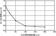
- FIG. 3A is a graph showing the relationship between the width of the injection suppression region 90 and the reverse recovery loss.
- the width of the injection suppression region 90 refers to the distance between the end portion of the transistor portion 70 and the end portion of the diode portion 80 in the arrangement direction (X-axis direction of FIGS. 1A to 2C).
- the width of the injection suppression region 90 is 0, it corresponds to the semiconductor device 1100 according to the comparative example, in which the injection suppression region 90 is not provided and the transistor portion 70 and the diode portion 80 are adjacent to each other.
- the reverse recovery loss decreases as the width of the injection suppression region 90 increases, and the reverse recovery loss decreases by about 36.5% when the width of the injection suppression region 90 increases from 0 to 200 ⁇ m. ..
- FIG. 3B is a graph showing the relationship between the width of the injection suppression region 90 and the turn-on loss.
- the turn-on loss of the transistor portion 70 correlates with the reverse recovery loss because the reverse recovery current of the diode portion 80 of the opposite arm is added.
- increasing the width of the injection suppression region 90 from 0 to 200 ⁇ m reduces turn-on loss by 30.5%.
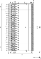
- FIG. 4A is a top view of the semiconductor device 100 according to the first embodiment of the present embodiment.
- FIG. 4A the positions where each member is projected onto the front surface 21 of the substrate 10 are shown. Note that FIG. 4A shows only a part of the members of the semiconductor device 100, and some members are omitted.
- the substrate 10 of the semiconductor device 100 has two sets of end sides 102 facing each other in a top view.
- the X-axis and the Y-axis are parallel to either end 102.
- the substrate 10 is provided with an active region 160.
- the active region 160 is a region in which the main current flows in the depth direction from the emitter region 12 of the substrate 10 when the semiconductor device 100 operates.
- the region surrounded by the gate runner 48 in the top view may be the active region 160.
- An emitter electrode is provided above the active region 160, but it is omitted in FIG. 4A.
- At least one of the transistor portion 70 and the diode portion 80 is provided in the active region 160.
- the transistor portion 70 and the diode portion 80 of this example are alternately arranged along a predetermined arrangement direction (X-axis direction in this example) on the front surface 21 of the substrate 10.
- the active region 160 may be provided with only one of the transistor portion 70 and the diode portion 80.
- the semiconductor device 100 may have one or more pads above the substrate 10.
- the semiconductor device 100 shown in FIG. 4A has a gate pad G in the active region 160.
- the gate pad G may be connected to an external circuit via wiring such as a wire.
- a gate potential is applied to the gate pad G.
- the gate pad G and the gate runner 48 are electrically connected, and the gate runner 48 surrounds the active region 160 and is electrically connected to the gate conductive portion of the gate trench portion 40 of the active region 160.
- the gate runner 48 is arranged between the active region 160 and the edge termination structure 190 of the substrate 10 in a top view.
- the gate runner 48 may be formed of a metal containing aluminum as a main component, such as polysilicon and an aluminum-silicon alloy.
- the semiconductor device 100 of this example includes an edge termination structure 190 between the active region 160 and the end side 102.
- the edge end structure portion 190 of this example is arranged between the gate runner 48 and the end side 102.
- the edge termination structure 190 relaxes the electric field concentration on the front surface 21 side of the substrate 10.
- the edge termination structure 190 may have a plurality of guard rings.
- the guard ring is a P-shaped region in contact with the front surface 21 of the substrate 10. By providing a plurality of guard rings, the depletion layer on the upper surface side of the active region 160 can be extended outward, and the withstand voltage of the semiconductor device 100 can be ensured.
- the edge termination structure 190 may further include at least one of a field plate and a resurf provided in an annular shape surrounding the gate runner 48.
- the semiconductor device 100 includes a temperature sense unit (not shown) which is a PN junction diode made of polysilicon or the like, and a current detection unit (not shown) which operates in the same manner as a transistor unit provided in the active region 160. You may.
- FIG. 4B is an enlarged view of part A of FIG. 4A.
- FIG. 4B shows an example in which one injection suppression region 90 is viewed from above (Z-axis positive side in FIG. 4B) to downward (Z-axis negative side).
- the injection suppression region 90 is also provided between the extension direction (Y-axis direction) end of the diode portion 80 and the outer circumference (gate runner 48) of the active region 160. That is, when viewed from above, the diode portion 80 is surrounded by the injection suppression region 90 at both the extension direction end portion and the arrangement direction (X-axis direction) end portion.
- the area of the substrate 10 is similarly expanded by S2.
- the diode does not increase the area of the substrate 10.
- the area S1 of the portion 80 may be reduced. Therefore, the ratio of the area S1 of the diode portion 80 may be 10% or more with respect to the total area (S1 + S2) of the diode portion 80 and the injection suppression region 90.
- the total area of the diode portion 80 may be 1.4% or more and 22% or less of the area of the semiconductor device 100 in top view.
- FIG. 4C is a graph showing the relationship between the width of the injection suppression region 90 and the reverse recovery loss.
- the solid line shows the reverse recovery loss when the area of the diode portion 80 is fixed and the area of the transistor portion 70 (that is, the width of the collector region 22) is reduced according to the increase in the width of the injection suppression region 90.
- the reverse recovery loss decreases by about 30%, whereas the area of the diode portion 80 is fixed. If so, the reduction in reverse recovery loss was only 21%. As described above, it can be seen that the reverse recovery loss is significantly reduced by 9% when the area of the diode portion 80 is reduced as compared with the case where the area of the diode portion 80 is fixed.
- FIG. 5A is a partial cross-sectional view of the semiconductor device 200 according to the second embodiment of the present embodiment.
- the same reference numerals are given to the elements common to the semiconductor device 100, and the description thereof will be omitted.
- the injection suppression region 90 of the semiconductor device 200 is provided with a second conductive type base region 94 instead of the base region 14.
- the doping concentration of the base region 94 may be 1 ⁇ e 16 cm -3 or more and 5 ⁇ e 19 cm -3 or less.
- the doping concentration of the base region 14 may be 1 ⁇ e 16 cm -3 or more and 1 ⁇ e 18 cm -3 or less, and the doping concentration of the extraction region 15 is 5 ⁇ e 18 cm -3 or more and 5 ⁇ e. It may be 20 cm -3 or less.
- the effect of suppressing hole injection from the transistor portion 70 can be enhanced. If the concentration of the base region 14 is lower than that of the base region 94, the effect of suppressing hole injection can be further enhanced.
- the processing method for separating the doping concentrations of the base region 14 and the base region 94 is as follows. If the doping concentration of the base region 94 is higher than the base region 14, both the base region 14 and 94 are doped, and then a mask is used for the base region 14 to open the base region 94 for doping. On the other hand, when the doping concentration of the base region 94 is lower than that of the base region 14, the base region 14 and the base region 94 are doped by using separate masks for processing.
- the same mask can be used for processing. Therefore, it is not necessary to add a mask, and it is possible to improve the workability and reduce the cost of the chip by reducing the mask.
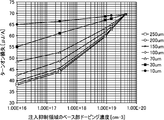
- FIG. 5B is a graph showing the relationship between the doping concentration in the base region 94 of the injection suppression region 90 and the reverse recovery loss.
- boron is injected as an impurity.
- the width of the injection suppression region 90 is set in 7 patterns in the range of 10 ⁇ m to 250 ⁇ m, and the doping concentration of boron in the base region 94 is reduced from e 19 cm -3 order to e 16 cm -3 order in each pattern. , See the change in reverse recovery loss.
- the improvement width of the reverse recovery loss is 1.2% regardless of the width of any injection suppression region 90. , No big difference is seen.
- the doping concentration of the base region 94 is lowered from the reference concentration, the dependence on the width of the injection suppression region 90 increases, and the reverse recovery loss is significantly reduced.
- the reverse recovery loss is reduced by about 5.9% in the pattern in which the width of the injection suppression region 90 is 10 ⁇ m, and the reverse recovery loss at the reference concentration is reduced. There is no big difference. On the other hand, in the pattern in which the width of the injection suppression region 90 is 250 ⁇ m, the reverse recovery loss is significantly reduced to about 46%.
- FIG. 5C is a graph showing the relationship between the doping concentration in the base region 94 of the injection suppression region 90 and the turn-on loss. Since the setting of the width of the injection suppression region 90 is common to FIG. 5B, the description thereof will be omitted.
- FIG. 6A is a partial top view of the semiconductor device 300 according to the third embodiment of the present embodiment.
- the same reference numerals are given to the elements common to the semiconductor device 100, and the description thereof will be omitted.
- the injection suppression region 90 of the semiconductor device 300 has a dummy trench portion 30 and does not have a gate trench portion 40, similarly to the semiconductor devices 100 and 200. However, unlike the semiconductor devices 100 and 200, the injection suppression region 90 of the semiconductor device 300 has an emitter region 12 and a extraction region 15 exposed on the front surface 21. However, the ratio of the emitter region 12 and the extraction region 15 in the injection suppression region 90 is lower than the ratio of the emitter region 12 and the extraction region 15 in the transistor portion 70.
- the emitter region 12 and the extraction region 15 are smaller in the injection suppression region 90 than in the transistor portion 70. Further, in the injection suppression region 90, a base region 14 is provided in a portion where the emitter region 12 and the extraction region 15 are not provided.
- the emitter region 12 and the extraction region 15 are alternately arranged in the stretching direction (Y-axis direction in FIG. 6A), but in the injection suppression region 90, the extraction region 15 is arranged around the emitter region 12. , A base region 14 is provided around the base region 14.
- the injection suppression region 90 of the semiconductor devices 100 and 200 does not have the emitter region 12, no electron current flows from the emitter region 12, but in the semiconductor device 300, the injection suppression region 90 has the emitter region 12, so that the electrons Current flows. Therefore, the on-voltage can be reduced as compared with the semiconductor devices 100 and 200.
- FIG. 6B is an enlarged view of a portion B in FIG. 6A.
- the arrangement of the emitter region 12 and the extraction region 15 in the injection suppression region 90 will be mainly described.
- the mesa portion adjacent to the injection suppression region 90 is designated as the first mesa portion 60a, and among the mesa portions 60 of the injection suppression region 90, the mesa portion adjacent to the transistor portion 70
- the mesa portion adjacent to the second mesa portion 60b, the second mesa portion 60b is referred to as the third mesa portion 60c, and the mesa portion adjacent to the diode portion 80 is referred to as the fourth mesa portion 60d.
- the injection suppression region 90 of this example has three mesa portions, a second mesa portion 60b to a fourth mesa portion 60d, but the number of the mesa portions is not limited to this.
- either the emitter region 12 or the extraction region 15 is arranged so as to be adjacent to each of the emitter regions 12 arranged in the adjacent mesa portions on the negative side of the X axis. Will be done.
- first mesa portion 60a six emitter regions 12 and six extraction regions 15 are alternately arranged in the Y-axis direction. Of the six emitter regions 12 of the first mesa portion 60a, every other three emitter regions 12 are adjacent to the three emitter regions 12 arranged in the second mesa portion 60b, and the remaining three emitter regions 12 Is adjacent to each of the three extraction regions 15 arranged in the second mesa portion 60b.
- the three emitter regions 12 of the second mesa portion 60b are adjacent to the three emitter regions 12 of the third mesa portion 60c, respectively.
- the extraction region 15 may be arranged in the third mesa portion 60c instead of a part of the arranged three emitter regions 12.
- the emitter region 12 is adjacent to the extraction region 15 in the Y-axis direction. That is, the emitter region 12 is surrounded by the extraction region 15 on the positive and negative sides of the Y-axis. As a result, the holes generated by the conductivity modulation can be extracted to the extraction region 15, so that the latch-up resistance can be improved.
- the base region 14 is arranged in the region where the emitter region 12 and the extraction region 15 are not arranged.
- the emitter region 12 is not arranged in the fourth mesa portion 60d.
- a pull-out region 15 is arranged in the fourth mesa portion 60d, and is adjacent to the emitter region 12 of the third mesa portion 60c adjacent to each other on the negative side of the X-axis.
- the base region 14 is arranged in the region where the drawing region 15 is not arranged.
- the emitter region 12 is not arranged in the third mesa portion 60c adjacent to the fourth mesa portion 60d on the negative side of the X-axis, only the base region 14 may be arranged in the fourth mesa portion 60d.
- the ratio of the pull-out region 15 in each mesa portion of the injection suppression region 90 is less than or equal to the ratio of the pull-out region 15 in the adjacent mesa portion on the negative side of the X-axis. That is, the ratio of the pull-out region 15 in the second mesa portion 60b is equal to or less than the ratio of the pull-out region 15 in the first mesa portion 60a. The ratio of the pulled-out region 15 in the third mesa portion 60c is equal to or less than the ratio of the pulled-out region 15 in the second mesa portion 60b.
- the ratio of the drawn region 15 in the fourth mesa portion 60d is equal to or less than the ratio of the drawn region 15 in the third mesa portion 60c, and more than the ratio of the drawn region 15 in the mesa portion 61 of the adjacent diode portion 80 on the positive side of the X axis. Is.
- the number of the third mesa portions 60c may be increased. By increasing the number of the third mesa portions 60c, the ratio of the extraction region 15 in the injection suppression region 90 can be reduced, so that the reverse recovery loss and the turn-on loss can be reduced.
- the emitter region 12 is provided in the third mesa portion 60c, the area of the region that operates as the transistor portion is increased, and the on-voltage can be reduced.
- the extraction region 15 of the injection suppression region 90 is arranged over the entire mesa portion in the X-axis direction, but may be about half the length of the mesa portion in the X-axis direction. ..
- the length of the extraction region 15 in the X-axis direction may be 0.3 ⁇ m or more.
- the length of the extraction region 15 in the Y-axis direction is equal to or less than the length of the extraction region 15 of the transistor portion 70 in the Y-axis direction.
- the length of the extraction region 15 in the Y-axis direction may be 0.5 ⁇ m or more.
- a plug region 17 is arranged in the hatched portion of the contact hole 54 shown in FIG. 6B.
- FIG. 7A is a partial top view of the semiconductor device 400 according to the fourth embodiment of the present embodiment.
- FIG. 7B is a diagram showing a cross section taken along the line aa'in FIG. 7A.
- the same reference numerals are given to the elements common to the semiconductor device 100, and the description thereof will be omitted.
- the transistor portion 70 is provided with a plurality of gate trench portions 40 along the arrangement direction
- the diode portion 80 is provided with a plurality of dummy trench portions 30 along the arrangement direction.
- the transistor portion 70 of this example has a full gate structure in which the dummy trench portion 30 is not provided.
- Each of the gate trench portions 40 is connected to the adjacent gate trench portion 40 via the tip portion 41.
- FIG. 7C is a diagram for explaining the operation of the diode portion 80 of the semiconductor device 400 at the time of conduction.
- FIG. 7C shows a'a'cross section of FIG. 7A, similar to FIG. 7B.
- the same reference numerals are given to the elements common to the semiconductor device 100, and the description thereof will be omitted.
- FIG. 8A is a partial cross-sectional view of the semiconductor device 500 according to the fifth embodiment of the present embodiment.
- FIG. 8A is a diagram showing a'a'cross sections in FIGS. 8B and 8C described later.
- the aa'cross section is an XZ plane that includes a gate trench 40 and a dummy trench 30 and passes through a drawing region 15 and a base region 14.
- the same reference numerals are given to the elements common to the semiconductor device 100, and the description thereof will be omitted.
- the transistor portion 70 of this example has a gate trench portion 40 and a dummy trench portion 30 provided along the X-axis direction.
- the gate insulating film 42 and the dummy insulating film 32 are omitted.
- the injection suppression region 90 of this example has a gate trench portion 40 and a dummy trench portion 30 provided along the X-axis direction, unlike the semiconductor devices 100 to 400.
- the dummy ratio in the injection suppression region 90 is higher than the dummy ratio in the transistor portion 70.
- the dummy ratio means the ratio of the number of dummy trench portions 30 to the total number of gate trench portions 40 and dummy trench portions 30.
- one gate trench portion 40 and two dummy trench portions 30 are alternately arranged in the X-axis direction.
- the dummy ratio of such an arrangement is about 67%.
- one gate trench portion 40 and three dummy trench portions 30 are alternately arranged in the X-axis direction.
- the dummy ratio of such an arrangement is 75%.
- the diode portion 80 has a dummy trench portion 30 provided along the X-axis direction and does not have a gate trench portion 40. Therefore, the dummy ratio of the diode portion 80 is 100%.
- the dummy ratio of the diode portion 80 is higher than the dummy ratio of the injection suppression region 90, and the dummy ratio of the injection suppression region 90 is higher than the dummy ratio of the transistor portion 70.
- a dummy trench portion 30 is arranged at the boundary between the transistor portion 70 and the injection suppression region 90, but the present invention is not limited to this.
- a gate trench portion 40 may be arranged at the boundary between the transistor portion 70 and the injection suppression region 90.
- a dummy trench portion 30 may be arranged at the boundary between the injection suppression region 90 and the diode portion 80.
- the plug is provided in the contact hole in contact with the drawing region 15 or the base region 14. Further, under the contact hole of the plug, a P ++ type plug region 17 having a doping concentration higher than that of the withdrawal region 15 is formed.
- FIG. 8B is a partial top view of the semiconductor device 500.
- FIG. 8B shows the transistor portion 70 at the center.
- the transistor portion 70 of this example has a gate trench portion 40 and a dummy trench portion 30 provided along the X-axis direction.
- the straight portion 29 of the two dummy trench portions 30 is arranged between the straight portions 39 of the two gate trench portions 40.
- the tip 41 connects the ends of the two straight portions 39 in the Y-axis direction to the gate runner 48.
- the dummy ratio of the transistor unit 70 is 0% or more and 75% or less.
- the ratio of the number of gate trench portions 40 to the number of dummy trench portions 30 may be 1: 0 (so-called full gate structure), and 1: 1 (one gate trench portion 40 and one).
- the dummy trench portions 30 of the above may be arranged alternately in the X-axis direction), and 1: 2 (one gate trench portion 40 and two dummy trench portions 30 are alternately arranged in the X-axis direction). It may be a structure in which it is arranged), and it may be 1: 3 (a structure in which one gate trench portion 40 and three dummy trench portions 30 are alternately arranged in the X-axis direction).
- FIG. 8C is a partial top view of the semiconductor device 500.
- FIG. 8C shows the injection suppression region 90 as the center.
- the injection suppression region 90 of this example has a gate trench portion 40 and a dummy trench portion 30 provided along the X-axis direction.
- the straight portions 29 of the three dummy trench portions 30 are arranged between the straight portions 39 of the two gate trench portions 40.
- the tip 41 connects the ends of the two straight portions 39 in the Y-axis direction to the gate runner 48.
- the emitter region 12 is arranged in the mesa portion 60 adjacent to the gate trench portion 40. Further, in the injection suppression region 90, the emitter region 12 and the extraction region 15 are alternately arranged in the Y-axis direction.
- the base region 14 is arranged in the portion where the emitter region 12 and the extraction region 15 are not arranged. That is, in the injection suppression region 90, the emitter region 12 and the extraction region 15 are not arranged in the mesa portion 60 adjacent to the dummy trench portion 30, but the base region 14 is arranged.
- the dummy ratio of the injection suppression region 90 is higher than that of the transistor portion 70, and the emitter region 12 and the extraction region 15 are arranged in the mesa portion 60 adjacent to the gate trench portion 40. Therefore, the ratio of the emitter region 12 and the extraction region 15 in the injection suppression region 90 is lower than that of the transistor portion 70. This suppresses hole injection and improves reverse recovery loss.
- the injection suppression region 90 since the injection suppression region 90 has an emitter region 12, an electron current flows. As a result, the injection suppression region 90 partially performs the transistor operation, and the deterioration of the on-voltage can be suppressed.
- the emitter region 12 is surrounded by the extraction region 15 on the positive side and the negative side of the Y axis. As a result, the holes generated by the conductivity modulation can be extracted to the extraction region 15, so that the latch-up resistance can be improved.
- the dummy ratio of the injection suppression region 90 is 75% or more and 87.5% or less.
- the ratio of the number of gate trench portions 40 to the number of dummy trench portions 30 is 1: 3 (one gate trench portion 40 and three dummy trench portions 30 alternate in the X-axis direction. It may be 1: 4 (a structure in which one gate trench portion 40 and four dummy trench portions 30 are alternately arranged in the X-axis direction). It may be 5 (a structure in which one gate trench portion 40 and five dummy trench portions and 30 are alternately arranged in the X-axis direction), and 1: 6 (one gate trench portion 40 and six).
- the structure may be such that the dummy trench portions 30 are alternately arranged in the X-axis direction), and 1: 7 (one gate trench portion 40 and seven dummy trench portions 30 are alternately arranged in the X-axis direction).
- the structure to be used) may be used.
- FIG. 8D is a partial top view of the semiconductor device 500.
- FIG. 8D shows the injection suppression region 90 as the center, as in FIG. 8C.
- FIG. 8D shows variations in the arrangement of the gate trench portion 40 and the dummy trench portion 30 in the injection suppression region 90. The description of the configuration common to FIG. 8C will be omitted.
- the straight portions 29 of the seven dummy trench portions 30 are arranged between the straight portions 39 of the two gate trench portions 40.
- the tip 41 connects the ends of the two straight portions 39 in the Y-axis direction to the gate runner 48.
- one gate trench portion 40 and seven dummy trench portions 30 are alternately arranged in the X-axis direction.
- the dummy ratio of such an arrangement is 87.5%.
- FIG. 8C shows an arrangement in which the dummy ratio of the injection suppression region 90 is minimized (a structure in which one gate trench portion 40 and three dummy trench portions 30 are alternately arranged in the X-axis direction).
- FIG. 8D shows an arrangement in which the dummy ratio of the injection suppression region 90 is maximized (a structure in which one gate trench portion 40 and seven dummy trench portions 30 are alternately arranged in the X-axis direction).
- the dummy ratio of the injection suppression region 90 is set higher than that of the transistor portion 70, and the injection suppression region 90 is turned on by partially performing the transistor operation by setting the dummy ratio in the range shown in FIGS. 8C to 8D. It is possible to suppress hole injection and improve reverse recovery loss while suppressing voltage deterioration.
Landscapes
- Metal-Oxide And Bipolar Metal-Oxide Semiconductor Integrated Circuits (AREA)
Priority Applications (4)
| Application Number | Priority Date | Filing Date | Title |
|---|---|---|---|
| CN202080047123.4A CN114097079A (zh) | 2020-01-17 | 2020-11-30 | 半导体装置 |
| DE112020002890.9T DE112020002890T5 (de) | 2020-01-17 | 2020-11-30 | Halbleitervorrichtung |
| JP2021570670A JP7231065B2 (ja) | 2020-01-17 | 2020-11-30 | 半導体装置 |
| US17/646,136 US12471303B2 (en) | 2020-01-17 | 2021-12-27 | Semiconductor device having an injection suppression region |
Applications Claiming Priority (4)
| Application Number | Priority Date | Filing Date | Title |
|---|---|---|---|
| JP2020006095 | 2020-01-17 | ||
| JP2020-006095 | 2020-01-17 | ||
| JP2020-085521 | 2020-05-14 | ||
| JP2020085521 | 2020-05-14 |
Related Child Applications (1)
| Application Number | Title | Priority Date | Filing Date |
|---|---|---|---|
| US17/646,136 Continuation US12471303B2 (en) | 2020-01-17 | 2021-12-27 | Semiconductor device having an injection suppression region |
Publications (1)
| Publication Number | Publication Date |
|---|---|
| WO2021145080A1 true WO2021145080A1 (ja) | 2021-07-22 |
Family
ID=76864229
Family Applications (1)
| Application Number | Title | Priority Date | Filing Date |
|---|---|---|---|
| PCT/JP2020/044532 Ceased WO2021145080A1 (ja) | 2020-01-17 | 2020-11-30 | 半導体装置 |
Country Status (5)
| Country | Link |
|---|---|
| US (1) | US12471303B2 (https=) |
| JP (1) | JP7231065B2 (https=) |
| CN (1) | CN114097079A (https=) |
| DE (1) | DE112020002890T5 (https=) |
| WO (1) | WO2021145080A1 (https=) |
Cited By (2)
| Publication number | Priority date | Publication date | Assignee | Title |
|---|---|---|---|---|
| JP2023026911A (ja) * | 2021-08-16 | 2023-03-01 | 三菱電機株式会社 | 半導体装置 |
| JP2024135983A (ja) * | 2023-03-23 | 2024-10-04 | 株式会社東芝 | 半導体装置 |
Families Citing this family (2)
| Publication number | Priority date | Publication date | Assignee | Title |
|---|---|---|---|---|
| JP7446198B2 (ja) * | 2020-10-01 | 2024-03-08 | 三菱電機株式会社 | 半導体装置 |
| CN117650165B (zh) * | 2023-10-31 | 2024-05-31 | 海信家电集团股份有限公司 | 半导体装置 |
Citations (6)
| Publication number | Priority date | Publication date | Assignee | Title |
|---|---|---|---|---|
| JP2012156564A (ja) * | 2008-12-24 | 2012-08-16 | Denso Corp | 半導体装置 |
| JP2012182391A (ja) * | 2011-03-02 | 2012-09-20 | Toyota Motor Corp | 半導体装置 |
| JP2014103376A (ja) * | 2012-09-24 | 2014-06-05 | Toshiba Corp | 半導体装置 |
| WO2019078131A1 (ja) * | 2017-10-18 | 2019-04-25 | 富士電機株式会社 | 半導体装置 |
| WO2019116748A1 (ja) * | 2017-12-14 | 2019-06-20 | 富士電機株式会社 | 半導体装置およびその製造方法 |
| JP2019161168A (ja) * | 2018-03-16 | 2019-09-19 | 富士電機株式会社 | 半導体装置 |
Family Cites Families (27)
| Publication number | Priority date | Publication date | Assignee | Title |
|---|---|---|---|---|
| JP2005057235A (ja) | 2003-07-24 | 2005-03-03 | Mitsubishi Electric Corp | 絶縁ゲート型バイポーラトランジスタ及びその製造方法、並びに、インバータ回路 |
| JP4799829B2 (ja) | 2003-08-27 | 2011-10-26 | 三菱電機株式会社 | 絶縁ゲート型トランジスタ及びインバータ回路 |
| JP2008192737A (ja) | 2007-02-02 | 2008-08-21 | Denso Corp | 半導体装置 |
| JP4910894B2 (ja) | 2007-06-12 | 2012-04-04 | 富士電機株式会社 | 半導体装置の製造方法および半導体装置 |
| EP2003694B1 (en) | 2007-06-14 | 2011-11-23 | Denso Corporation | Semiconductor device |
| JP5045733B2 (ja) | 2008-12-24 | 2012-10-10 | 株式会社デンソー | 半導体装置 |
| KR101276407B1 (ko) | 2010-05-07 | 2013-06-19 | 도요타지도샤가부시키가이샤 | 반도체 장치 |
| JP5582102B2 (ja) | 2010-07-01 | 2014-09-03 | 株式会社デンソー | 半導体装置 |
| JP5605073B2 (ja) | 2010-08-17 | 2014-10-15 | 株式会社デンソー | 半導体装置 |
| JP5321669B2 (ja) | 2010-11-25 | 2013-10-23 | 株式会社デンソー | 半導体装置 |
| JP6022774B2 (ja) | 2012-01-24 | 2016-11-09 | トヨタ自動車株式会社 | 半導体装置 |
| JP5787853B2 (ja) | 2012-09-12 | 2015-09-30 | 株式会社東芝 | 電力用半導体装置 |
| US9960165B2 (en) | 2013-11-05 | 2018-05-01 | Toyota Jidosha Kabushiki Kaisha | Semiconductor device having adjacent IGBT and diode regions with a shifted boundary plane between a collector region and a cathode region |
| JP6119593B2 (ja) | 2013-12-17 | 2017-04-26 | トヨタ自動車株式会社 | 半導体装置 |
| JP6421570B2 (ja) * | 2013-12-20 | 2018-11-14 | 株式会社デンソー | 半導体装置 |
| KR101921844B1 (ko) | 2014-08-26 | 2019-02-13 | 미쓰비시덴키 가부시키가이샤 | 반도체 소자 |
| JP6197773B2 (ja) | 2014-09-29 | 2017-09-20 | トヨタ自動車株式会社 | 半導体装置 |
| JP6260515B2 (ja) | 2014-11-13 | 2018-01-17 | 三菱電機株式会社 | 半導体装置 |
| JP6274154B2 (ja) | 2015-05-27 | 2018-02-07 | トヨタ自動車株式会社 | 逆導通igbt |
| JP6334465B2 (ja) * | 2015-06-17 | 2018-05-30 | 富士電機株式会社 | 半導体装置 |
| JP6844147B2 (ja) * | 2016-02-12 | 2021-03-17 | 富士電機株式会社 | 半導体装置 |
| JP6878848B2 (ja) * | 2016-02-16 | 2021-06-02 | 富士電機株式会社 | 半導体装置 |
| US10559663B2 (en) * | 2016-10-14 | 2020-02-11 | Fuji Electric Co., Ltd. | Semiconductor device with improved current flow distribution |
| CN109075202B (zh) | 2016-11-17 | 2021-08-31 | 富士电机株式会社 | 半导体装置 |
| EP3480855B1 (en) | 2017-02-15 | 2023-09-20 | Fuji Electric Co., Ltd. | Semiconductor device |
| US10319808B2 (en) | 2017-04-03 | 2019-06-11 | Fuji Electric Co., Ltd. | Semiconductor device |
| JP7095303B2 (ja) * | 2018-02-14 | 2022-07-05 | 富士電機株式会社 | 半導体装置 |
-
2020
- 2020-11-30 JP JP2021570670A patent/JP7231065B2/ja active Active
- 2020-11-30 CN CN202080047123.4A patent/CN114097079A/zh active Pending
- 2020-11-30 DE DE112020002890.9T patent/DE112020002890T5/de active Pending
- 2020-11-30 WO PCT/JP2020/044532 patent/WO2021145080A1/ja not_active Ceased
-
2021
- 2021-12-27 US US17/646,136 patent/US12471303B2/en active Active
Patent Citations (6)
| Publication number | Priority date | Publication date | Assignee | Title |
|---|---|---|---|---|
| JP2012156564A (ja) * | 2008-12-24 | 2012-08-16 | Denso Corp | 半導体装置 |
| JP2012182391A (ja) * | 2011-03-02 | 2012-09-20 | Toyota Motor Corp | 半導体装置 |
| JP2014103376A (ja) * | 2012-09-24 | 2014-06-05 | Toshiba Corp | 半導体装置 |
| WO2019078131A1 (ja) * | 2017-10-18 | 2019-04-25 | 富士電機株式会社 | 半導体装置 |
| WO2019116748A1 (ja) * | 2017-12-14 | 2019-06-20 | 富士電機株式会社 | 半導体装置およびその製造方法 |
| JP2019161168A (ja) * | 2018-03-16 | 2019-09-19 | 富士電機株式会社 | 半導体装置 |
Cited By (4)
| Publication number | Priority date | Publication date | Assignee | Title |
|---|---|---|---|---|
| JP2023026911A (ja) * | 2021-08-16 | 2023-03-01 | 三菱電機株式会社 | 半導体装置 |
| JP7609010B2 (ja) | 2021-08-16 | 2025-01-07 | 三菱電機株式会社 | 半導体装置 |
| US12328933B2 (en) | 2021-08-16 | 2025-06-10 | Mitsubishi Electric Corporation | Semiconductor device |
| JP2024135983A (ja) * | 2023-03-23 | 2024-10-04 | 株式会社東芝 | 半導体装置 |
Also Published As
| Publication number | Publication date |
|---|---|
| US20220149191A1 (en) | 2022-05-12 |
| JP7231065B2 (ja) | 2023-03-01 |
| US12471303B2 (en) | 2025-11-11 |
| CN114097079A (zh) | 2022-02-25 |
| JPWO2021145080A1 (https=) | 2021-07-22 |
| DE112020002890T5 (de) | 2022-02-24 |
Similar Documents
| Publication | Publication Date | Title |
|---|---|---|
| US11532738B2 (en) | Semiconductor device | |
| JP7456520B2 (ja) | 半導体装置 | |
| JP6733829B2 (ja) | 半導体装置 | |
| JP7211516B2 (ja) | 半導体装置 | |
| JP2014056942A (ja) | 電力用半導体装置 | |
| US12471303B2 (en) | Semiconductor device having an injection suppression region | |
| JPWO2019116748A1 (ja) | 半導体装置およびその製造方法 | |
| JP7613570B2 (ja) | 半導体装置 | |
| WO2021075330A1 (ja) | 半導体装置および半導体装置の製造方法 | |
| JP2020177973A (ja) | 半導体装置 | |
| JP7459976B2 (ja) | 半導体装置 | |
| JP7384287B2 (ja) | 半導体装置 | |
| US20240120412A1 (en) | Semiconductor device | |
| WO2022239284A1 (ja) | 半導体装置 | |
| JP6996621B2 (ja) | 半導体装置 | |
| US12183789B2 (en) | Semiconductor device | |
| JP2023170200A (ja) | 半導体装置 | |
| JP7670132B2 (ja) | 半導体装置および半導体装置の製造方法 | |
| WO2023224059A1 (ja) | 半導体装置 | |
| CN117913137A (zh) | 半导体装置及半导体装置的制造方法 | |
| US20240072110A1 (en) | Semiconductor device and manufacturing method of semiconductor device | |
| JP2024118696A (ja) | 半導体装置および半導体装置の製造方法 | |
| WO2025079715A1 (ja) | 半導体装置および半導体装置の製造方法 | |
| WO2025033086A1 (ja) | 半導体装置 |
Legal Events
| Date | Code | Title | Description |
|---|---|---|---|
| 121 | Ep: the epo has been informed by wipo that ep was designated in this application |
Ref document number: 20913751 Country of ref document: EP Kind code of ref document: A1 |
|
| ENP | Entry into the national phase |
Ref document number: 2021570670 Country of ref document: JP Kind code of ref document: A |
|
| 122 | Ep: pct application non-entry in european phase |
Ref document number: 20913751 Country of ref document: EP Kind code of ref document: A1 |