WO2021145080A1 - 半導体装置 - Google Patents
半導体装置 Download PDFInfo
- Publication number
- WO2021145080A1 WO2021145080A1 PCT/JP2020/044532 JP2020044532W WO2021145080A1 WO 2021145080 A1 WO2021145080 A1 WO 2021145080A1 JP 2020044532 W JP2020044532 W JP 2020044532W WO 2021145080 A1 WO2021145080 A1 WO 2021145080A1
- Authority
- WO
- WIPO (PCT)
- Prior art keywords
- region
- semiconductor device
- injection suppression
- diode
- transistor
- Prior art date
Links
- 239000004065 semiconductor Substances 0.000 title claims abstract description 197
- 238000002347 injection Methods 0.000 claims abstract description 173
- 239000007924 injection Substances 0.000 claims abstract description 173
- 239000000758 substrate Substances 0.000 claims abstract description 103
- 230000001629 suppression Effects 0.000 claims description 152
- 238000000605 extraction Methods 0.000 claims description 73
- 238000003860 storage Methods 0.000 claims description 7
- 238000011084 recovery Methods 0.000 description 41
- 239000000370 acceptor Substances 0.000 description 19
- 239000010410 layer Substances 0.000 description 19
- 239000011229 interlayer Substances 0.000 description 15
- 229910052751 metal Inorganic materials 0.000 description 14
- 239000002184 metal Substances 0.000 description 14
- 238000000034 method Methods 0.000 description 14
- 239000012535 impurity Substances 0.000 description 10
- 230000007423 decrease Effects 0.000 description 8
- 238000010586 diagram Methods 0.000 description 8
- 230000000694 effects Effects 0.000 description 7
- 229910021420 polycrystalline silicon Inorganic materials 0.000 description 6
- 229920005591 polysilicon Polymers 0.000 description 6
- 230000004888 barrier function Effects 0.000 description 5
- 239000000126 substance Substances 0.000 description 5
- ZOXJGFHDIHLPTG-UHFFFAOYSA-N Boron Chemical compound [B] ZOXJGFHDIHLPTG-UHFFFAOYSA-N 0.000 description 4
- XUIMIQQOPSSXEZ-UHFFFAOYSA-N Silicon Chemical compound [Si] XUIMIQQOPSSXEZ-UHFFFAOYSA-N 0.000 description 4
- 229910052782 aluminium Inorganic materials 0.000 description 4
- XAGFODPZIPBFFR-UHFFFAOYSA-N aluminium Chemical compound [Al] XAGFODPZIPBFFR-UHFFFAOYSA-N 0.000 description 4
- 229910052796 boron Inorganic materials 0.000 description 4
- 230000000052 comparative effect Effects 0.000 description 4
- 229910052710 silicon Inorganic materials 0.000 description 4
- 239000010703 silicon Substances 0.000 description 4
- WFKWXMTUELFFGS-UHFFFAOYSA-N tungsten Chemical compound [W] WFKWXMTUELFFGS-UHFFFAOYSA-N 0.000 description 4
- 229910052721 tungsten Inorganic materials 0.000 description 4
- 239000010937 tungsten Substances 0.000 description 4
- OAICVXFJPJFONN-UHFFFAOYSA-N Phosphorus Chemical compound [P] OAICVXFJPJFONN-UHFFFAOYSA-N 0.000 description 3
- 230000007547 defect Effects 0.000 description 3
- 239000002019 doping agent Substances 0.000 description 3
- 230000005684 electric field Effects 0.000 description 3
- 239000001257 hydrogen Substances 0.000 description 3
- 229910052739 hydrogen Inorganic materials 0.000 description 3
- 230000006872 improvement Effects 0.000 description 3
- 229910052698 phosphorus Inorganic materials 0.000 description 3
- 239000011574 phosphorus Substances 0.000 description 3
- 230000008569 process Effects 0.000 description 3
- UFHFLCQGNIYNRP-UHFFFAOYSA-N Hydrogen Chemical compound [H][H] UFHFLCQGNIYNRP-UHFFFAOYSA-N 0.000 description 2
- 229910000676 Si alloy Inorganic materials 0.000 description 2
- CSDREXVUYHZDNP-UHFFFAOYSA-N alumanylidynesilicon Chemical compound [Al].[Si] CSDREXVUYHZDNP-UHFFFAOYSA-N 0.000 description 2
- 229910052785 arsenic Inorganic materials 0.000 description 2
- RQNWIZPPADIBDY-UHFFFAOYSA-N arsenic atom Chemical compound [As] RQNWIZPPADIBDY-UHFFFAOYSA-N 0.000 description 2
- 239000004020 conductor Substances 0.000 description 2
- 239000013078 crystal Substances 0.000 description 2
- 230000006866 deterioration Effects 0.000 description 2
- 238000009792 diffusion process Methods 0.000 description 2
- 238000010894 electron beam technology Methods 0.000 description 2
- 230000001747 exhibiting effect Effects 0.000 description 2
- 150000002500 ions Chemical class 0.000 description 2
- 239000000463 material Substances 0.000 description 2
- 238000000691 measurement method Methods 0.000 description 2
- 238000005121 nitriding Methods 0.000 description 2
- 230000001590 oxidative effect Effects 0.000 description 2
- 229910002601 GaN Inorganic materials 0.000 description 1
- JMASRVWKEDWRBT-UHFFFAOYSA-N Gallium nitride Chemical compound [Ga]#N JMASRVWKEDWRBT-UHFFFAOYSA-N 0.000 description 1
- RTAQQCXQSZGOHL-UHFFFAOYSA-N Titanium Chemical compound [Ti] RTAQQCXQSZGOHL-UHFFFAOYSA-N 0.000 description 1
- KPSZQYZCNSCYGG-UHFFFAOYSA-N [B].[B] Chemical compound [B].[B] KPSZQYZCNSCYGG-UHFFFAOYSA-N 0.000 description 1
- 238000009825 accumulation Methods 0.000 description 1
- 230000004913 activation Effects 0.000 description 1
- 229910052787 antimony Inorganic materials 0.000 description 1
- WATWJIUSRGPENY-UHFFFAOYSA-N antimony atom Chemical compound [Sb] WATWJIUSRGPENY-UHFFFAOYSA-N 0.000 description 1
- QVGXLLKOCUKJST-UHFFFAOYSA-N atomic oxygen Chemical compound [O] QVGXLLKOCUKJST-UHFFFAOYSA-N 0.000 description 1
- 239000000969 carrier Substances 0.000 description 1
- 230000008859 change Effects 0.000 description 1
- 238000001514 detection method Methods 0.000 description 1
- 230000008034 disappearance Effects 0.000 description 1
- 238000009826 distribution Methods 0.000 description 1
- 230000005484 gravity Effects 0.000 description 1
- 239000001307 helium Substances 0.000 description 1
- 229910052734 helium Inorganic materials 0.000 description 1
- SWQJXJOGLNCZEY-UHFFFAOYSA-N helium atom Chemical compound [He] SWQJXJOGLNCZEY-UHFFFAOYSA-N 0.000 description 1
- 150000002431 hydrogen Chemical class 0.000 description 1
- 239000011810 insulating material Substances 0.000 description 1
- 238000004519 manufacturing process Methods 0.000 description 1
- 238000012986 modification Methods 0.000 description 1
- 230000004048 modification Effects 0.000 description 1
- 150000004767 nitrides Chemical class 0.000 description 1
- 239000001301 oxygen Substances 0.000 description 1
- 229910052760 oxygen Inorganic materials 0.000 description 1
- 230000035515 penetration Effects 0.000 description 1
- 239000011148 porous material Substances 0.000 description 1
- 238000003672 processing method Methods 0.000 description 1
- 230000001737 promoting effect Effects 0.000 description 1
- 238000005215 recombination Methods 0.000 description 1
- 230000006798 recombination Effects 0.000 description 1
- 230000009467 reduction Effects 0.000 description 1
- 238000001004 secondary ion mass spectrometry Methods 0.000 description 1
- 239000005368 silicate glass Substances 0.000 description 1
- HBMJWWWQQXIZIP-UHFFFAOYSA-N silicon carbide Chemical compound [Si+]#[C-] HBMJWWWQQXIZIP-UHFFFAOYSA-N 0.000 description 1
- 229910010271 silicon carbide Inorganic materials 0.000 description 1
- 239000002344 surface layer Substances 0.000 description 1
- 230000036413 temperature sense Effects 0.000 description 1
- 239000010936 titanium Substances 0.000 description 1
- 229910052719 titanium Inorganic materials 0.000 description 1
- 150000003609 titanium compounds Chemical class 0.000 description 1
Images


Classifications
-
- H—ELECTRICITY
- H01—ELECTRIC ELEMENTS
- H01L—SEMICONDUCTOR DEVICES NOT COVERED BY CLASS H10
- H01L29/00—Semiconductor devices specially adapted for rectifying, amplifying, oscillating or switching and having potential barriers; Capacitors or resistors having potential barriers, e.g. a PN-junction depletion layer or carrier concentration layer; Details of semiconductor bodies or of electrodes thereof ; Multistep manufacturing processes therefor
- H01L29/66—Types of semiconductor device ; Multistep manufacturing processes therefor
- H01L29/86—Types of semiconductor device ; Multistep manufacturing processes therefor controllable only by variation of the electric current supplied, or only the electric potential applied, to one or more of the electrodes carrying the current to be rectified, amplified, oscillated or switched
- H01L29/861—Diodes
- H01L29/8613—Mesa PN junction diodes
-
- H—ELECTRICITY
- H01—ELECTRIC ELEMENTS
- H01L—SEMICONDUCTOR DEVICES NOT COVERED BY CLASS H10
- H01L27/00—Devices consisting of a plurality of semiconductor or other solid-state components formed in or on a common substrate
- H01L27/02—Devices consisting of a plurality of semiconductor or other solid-state components formed in or on a common substrate including semiconductor components specially adapted for rectifying, oscillating, amplifying or switching and having potential barriers; including integrated passive circuit elements having potential barriers
- H01L27/04—Devices consisting of a plurality of semiconductor or other solid-state components formed in or on a common substrate including semiconductor components specially adapted for rectifying, oscillating, amplifying or switching and having potential barriers; including integrated passive circuit elements having potential barriers the substrate being a semiconductor body
- H01L27/06—Devices consisting of a plurality of semiconductor or other solid-state components formed in or on a common substrate including semiconductor components specially adapted for rectifying, oscillating, amplifying or switching and having potential barriers; including integrated passive circuit elements having potential barriers the substrate being a semiconductor body including a plurality of individual components in a non-repetitive configuration
- H01L27/07—Devices consisting of a plurality of semiconductor or other solid-state components formed in or on a common substrate including semiconductor components specially adapted for rectifying, oscillating, amplifying or switching and having potential barriers; including integrated passive circuit elements having potential barriers the substrate being a semiconductor body including a plurality of individual components in a non-repetitive configuration the components having an active region in common
- H01L27/0705—Devices consisting of a plurality of semiconductor or other solid-state components formed in or on a common substrate including semiconductor components specially adapted for rectifying, oscillating, amplifying or switching and having potential barriers; including integrated passive circuit elements having potential barriers the substrate being a semiconductor body including a plurality of individual components in a non-repetitive configuration the components having an active region in common comprising components of the field effect type
- H01L27/0727—Devices consisting of a plurality of semiconductor or other solid-state components formed in or on a common substrate including semiconductor components specially adapted for rectifying, oscillating, amplifying or switching and having potential barriers; including integrated passive circuit elements having potential barriers the substrate being a semiconductor body including a plurality of individual components in a non-repetitive configuration the components having an active region in common comprising components of the field effect type in combination with diodes, or capacitors or resistors
-
- H—ELECTRICITY
- H01—ELECTRIC ELEMENTS
- H01L—SEMICONDUCTOR DEVICES NOT COVERED BY CLASS H10
- H01L21/00—Processes or apparatus adapted for the manufacture or treatment of semiconductor or solid state devices or of parts thereof
- H01L21/70—Manufacture or treatment of devices consisting of a plurality of solid state components formed in or on a common substrate or of parts thereof; Manufacture of integrated circuit devices or of parts thereof
- H01L21/77—Manufacture or treatment of devices consisting of a plurality of solid state components or integrated circuits formed in, or on, a common substrate
- H01L21/78—Manufacture or treatment of devices consisting of a plurality of solid state components or integrated circuits formed in, or on, a common substrate with subsequent division of the substrate into plural individual devices
- H01L21/82—Manufacture or treatment of devices consisting of a plurality of solid state components or integrated circuits formed in, or on, a common substrate with subsequent division of the substrate into plural individual devices to produce devices, e.g. integrated circuits, each consisting of a plurality of components
- H01L21/822—Manufacture or treatment of devices consisting of a plurality of solid state components or integrated circuits formed in, or on, a common substrate with subsequent division of the substrate into plural individual devices to produce devices, e.g. integrated circuits, each consisting of a plurality of components the substrate being a semiconductor, using silicon technology
- H01L21/8232—Field-effect technology
- H01L21/8234—MIS technology, i.e. integration processes of field effect transistors of the conductor-insulator-semiconductor type
-
- H—ELECTRICITY
- H01—ELECTRIC ELEMENTS
- H01L—SEMICONDUCTOR DEVICES NOT COVERED BY CLASS H10
- H01L27/00—Devices consisting of a plurality of semiconductor or other solid-state components formed in or on a common substrate
- H01L27/02—Devices consisting of a plurality of semiconductor or other solid-state components formed in or on a common substrate including semiconductor components specially adapted for rectifying, oscillating, amplifying or switching and having potential barriers; including integrated passive circuit elements having potential barriers
- H01L27/04—Devices consisting of a plurality of semiconductor or other solid-state components formed in or on a common substrate including semiconductor components specially adapted for rectifying, oscillating, amplifying or switching and having potential barriers; including integrated passive circuit elements having potential barriers the substrate being a semiconductor body
- H01L27/06—Devices consisting of a plurality of semiconductor or other solid-state components formed in or on a common substrate including semiconductor components specially adapted for rectifying, oscillating, amplifying or switching and having potential barriers; including integrated passive circuit elements having potential barriers the substrate being a semiconductor body including a plurality of individual components in a non-repetitive configuration
-
- H—ELECTRICITY
- H01—ELECTRIC ELEMENTS
- H01L—SEMICONDUCTOR DEVICES NOT COVERED BY CLASS H10
- H01L27/00—Devices consisting of a plurality of semiconductor or other solid-state components formed in or on a common substrate
- H01L27/02—Devices consisting of a plurality of semiconductor or other solid-state components formed in or on a common substrate including semiconductor components specially adapted for rectifying, oscillating, amplifying or switching and having potential barriers; including integrated passive circuit elements having potential barriers
- H01L27/04—Devices consisting of a plurality of semiconductor or other solid-state components formed in or on a common substrate including semiconductor components specially adapted for rectifying, oscillating, amplifying or switching and having potential barriers; including integrated passive circuit elements having potential barriers the substrate being a semiconductor body
- H01L27/08—Devices consisting of a plurality of semiconductor or other solid-state components formed in or on a common substrate including semiconductor components specially adapted for rectifying, oscillating, amplifying or switching and having potential barriers; including integrated passive circuit elements having potential barriers the substrate being a semiconductor body including only semiconductor components of a single kind
- H01L27/085—Devices consisting of a plurality of semiconductor or other solid-state components formed in or on a common substrate including semiconductor components specially adapted for rectifying, oscillating, amplifying or switching and having potential barriers; including integrated passive circuit elements having potential barriers the substrate being a semiconductor body including only semiconductor components of a single kind including field-effect components only
- H01L27/088—Devices consisting of a plurality of semiconductor or other solid-state components formed in or on a common substrate including semiconductor components specially adapted for rectifying, oscillating, amplifying or switching and having potential barriers; including integrated passive circuit elements having potential barriers the substrate being a semiconductor body including only semiconductor components of a single kind including field-effect components only the components being field-effect transistors with insulated gate
-
- H—ELECTRICITY
- H01—ELECTRIC ELEMENTS
- H01L—SEMICONDUCTOR DEVICES NOT COVERED BY CLASS H10
- H01L29/00—Semiconductor devices specially adapted for rectifying, amplifying, oscillating or switching and having potential barriers; Capacitors or resistors having potential barriers, e.g. a PN-junction depletion layer or carrier concentration layer; Details of semiconductor bodies or of electrodes thereof ; Multistep manufacturing processes therefor
- H01L29/02—Semiconductor bodies ; Multistep manufacturing processes therefor
- H01L29/06—Semiconductor bodies ; Multistep manufacturing processes therefor characterised by their shape; characterised by the shapes, relative sizes, or dispositions of the semiconductor regions ; characterised by the concentration or distribution of impurities within semiconductor regions
- H01L29/0603—Semiconductor bodies ; Multistep manufacturing processes therefor characterised by their shape; characterised by the shapes, relative sizes, or dispositions of the semiconductor regions ; characterised by the concentration or distribution of impurities within semiconductor regions characterised by particular constructional design considerations, e.g. for preventing surface leakage, for controlling electric field concentration or for internal isolations regions
- H01L29/0607—Semiconductor bodies ; Multistep manufacturing processes therefor characterised by their shape; characterised by the shapes, relative sizes, or dispositions of the semiconductor regions ; characterised by the concentration or distribution of impurities within semiconductor regions characterised by particular constructional design considerations, e.g. for preventing surface leakage, for controlling electric field concentration or for internal isolations regions for preventing surface leakage or controlling electric field concentration
- H01L29/0611—Semiconductor bodies ; Multistep manufacturing processes therefor characterised by their shape; characterised by the shapes, relative sizes, or dispositions of the semiconductor regions ; characterised by the concentration or distribution of impurities within semiconductor regions characterised by particular constructional design considerations, e.g. for preventing surface leakage, for controlling electric field concentration or for internal isolations regions for preventing surface leakage or controlling electric field concentration for increasing or controlling the breakdown voltage of reverse biased devices
- H01L29/0615—Semiconductor bodies ; Multistep manufacturing processes therefor characterised by their shape; characterised by the shapes, relative sizes, or dispositions of the semiconductor regions ; characterised by the concentration or distribution of impurities within semiconductor regions characterised by particular constructional design considerations, e.g. for preventing surface leakage, for controlling electric field concentration or for internal isolations regions for preventing surface leakage or controlling electric field concentration for increasing or controlling the breakdown voltage of reverse biased devices by the doping profile or the shape or the arrangement of the PN junction, or with supplementary regions, e.g. junction termination extension [JTE]
- H01L29/0619—Semiconductor bodies ; Multistep manufacturing processes therefor characterised by their shape; characterised by the shapes, relative sizes, or dispositions of the semiconductor regions ; characterised by the concentration or distribution of impurities within semiconductor regions characterised by particular constructional design considerations, e.g. for preventing surface leakage, for controlling electric field concentration or for internal isolations regions for preventing surface leakage or controlling electric field concentration for increasing or controlling the breakdown voltage of reverse biased devices by the doping profile or the shape or the arrangement of the PN junction, or with supplementary regions, e.g. junction termination extension [JTE] with a supplementary region doped oppositely to or in rectifying contact with the semiconductor containing or contacting region, e.g. guard rings with PN or Schottky junction
-
- H—ELECTRICITY
- H01—ELECTRIC ELEMENTS
- H01L—SEMICONDUCTOR DEVICES NOT COVERED BY CLASS H10
- H01L29/00—Semiconductor devices specially adapted for rectifying, amplifying, oscillating or switching and having potential barriers; Capacitors or resistors having potential barriers, e.g. a PN-junction depletion layer or carrier concentration layer; Details of semiconductor bodies or of electrodes thereof ; Multistep manufacturing processes therefor
- H01L29/02—Semiconductor bodies ; Multistep manufacturing processes therefor
- H01L29/06—Semiconductor bodies ; Multistep manufacturing processes therefor characterised by their shape; characterised by the shapes, relative sizes, or dispositions of the semiconductor regions ; characterised by the concentration or distribution of impurities within semiconductor regions
- H01L29/0684—Semiconductor bodies ; Multistep manufacturing processes therefor characterised by their shape; characterised by the shapes, relative sizes, or dispositions of the semiconductor regions ; characterised by the concentration or distribution of impurities within semiconductor regions characterised by the shape, relative sizes or dispositions of the semiconductor regions or junctions between the regions
- H01L29/0692—Surface layout
- H01L29/0696—Surface layout of cellular field-effect devices, e.g. multicellular DMOS transistors or IGBTs
-
- H—ELECTRICITY
- H01—ELECTRIC ELEMENTS
- H01L—SEMICONDUCTOR DEVICES NOT COVERED BY CLASS H10
- H01L29/00—Semiconductor devices specially adapted for rectifying, amplifying, oscillating or switching and having potential barriers; Capacitors or resistors having potential barriers, e.g. a PN-junction depletion layer or carrier concentration layer; Details of semiconductor bodies or of electrodes thereof ; Multistep manufacturing processes therefor
- H01L29/66—Types of semiconductor device ; Multistep manufacturing processes therefor
- H01L29/66007—Multistep manufacturing processes
- H01L29/66075—Multistep manufacturing processes of devices having semiconductor bodies comprising group 14 or group 13/15 materials
- H01L29/66227—Multistep manufacturing processes of devices having semiconductor bodies comprising group 14 or group 13/15 materials the devices being controllable only by the electric current supplied or the electric potential applied, to an electrode which does not carry the current to be rectified, amplified or switched, e.g. three-terminal devices
- H01L29/66234—Bipolar junction transistors [BJT]
- H01L29/66325—Bipolar junction transistors [BJT] controlled by field-effect, e.g. insulated gate bipolar transistors [IGBT]
- H01L29/66333—Vertical insulated gate bipolar transistors
- H01L29/66348—Vertical insulated gate bipolar transistors with a recessed gate
-
- H—ELECTRICITY
- H01—ELECTRIC ELEMENTS
- H01L—SEMICONDUCTOR DEVICES NOT COVERED BY CLASS H10
- H01L29/00—Semiconductor devices specially adapted for rectifying, amplifying, oscillating or switching and having potential barriers; Capacitors or resistors having potential barriers, e.g. a PN-junction depletion layer or carrier concentration layer; Details of semiconductor bodies or of electrodes thereof ; Multistep manufacturing processes therefor
- H01L29/66—Types of semiconductor device ; Multistep manufacturing processes therefor
- H01L29/68—Types of semiconductor device ; Multistep manufacturing processes therefor controllable by only the electric current supplied, or only the electric potential applied, to an electrode which does not carry the current to be rectified, amplified or switched
- H01L29/70—Bipolar devices
- H01L29/72—Transistor-type devices, i.e. able to continuously respond to applied control signals
- H01L29/739—Transistor-type devices, i.e. able to continuously respond to applied control signals controlled by field-effect, e.g. bipolar static induction transistors [BSIT]
- H01L29/7393—Insulated gate bipolar mode transistors, i.e. IGBT; IGT; COMFET
- H01L29/7395—Vertical transistors, e.g. vertical IGBT
- H01L29/7396—Vertical transistors, e.g. vertical IGBT with a non planar surface, e.g. with a non planar gate or with a trench or recess or pillar in the surface of the emitter, base or collector region for improving current density or short circuiting the emitter and base regions
- H01L29/7397—Vertical transistors, e.g. vertical IGBT with a non planar surface, e.g. with a non planar gate or with a trench or recess or pillar in the surface of the emitter, base or collector region for improving current density or short circuiting the emitter and base regions and a gate structure lying on a slanted or vertical surface or formed in a groove, e.g. trench gate IGBT
-
- H—ELECTRICITY
- H01—ELECTRIC ELEMENTS
- H01L—SEMICONDUCTOR DEVICES NOT COVERED BY CLASS H10
- H01L29/00—Semiconductor devices specially adapted for rectifying, amplifying, oscillating or switching and having potential barriers; Capacitors or resistors having potential barriers, e.g. a PN-junction depletion layer or carrier concentration layer; Details of semiconductor bodies or of electrodes thereof ; Multistep manufacturing processes therefor
- H01L29/66—Types of semiconductor device ; Multistep manufacturing processes therefor
- H01L29/68—Types of semiconductor device ; Multistep manufacturing processes therefor controllable by only the electric current supplied, or only the electric potential applied, to an electrode which does not carry the current to be rectified, amplified or switched
- H01L29/76—Unipolar devices, e.g. field effect transistors
- H01L29/772—Field effect transistors
- H01L29/78—Field effect transistors with field effect produced by an insulated gate
-
- H—ELECTRICITY
- H01—ELECTRIC ELEMENTS
- H01L—SEMICONDUCTOR DEVICES NOT COVERED BY CLASS H10
- H01L29/00—Semiconductor devices specially adapted for rectifying, amplifying, oscillating or switching and having potential barriers; Capacitors or resistors having potential barriers, e.g. a PN-junction depletion layer or carrier concentration layer; Details of semiconductor bodies or of electrodes thereof ; Multistep manufacturing processes therefor
- H01L29/02—Semiconductor bodies ; Multistep manufacturing processes therefor
- H01L29/06—Semiconductor bodies ; Multistep manufacturing processes therefor characterised by their shape; characterised by the shapes, relative sizes, or dispositions of the semiconductor regions ; characterised by the concentration or distribution of impurities within semiconductor regions
- H01L29/08—Semiconductor bodies ; Multistep manufacturing processes therefor characterised by their shape; characterised by the shapes, relative sizes, or dispositions of the semiconductor regions ; characterised by the concentration or distribution of impurities within semiconductor regions with semiconductor regions connected to an electrode carrying current to be rectified, amplified or switched and such electrode being part of a semiconductor device which comprises three or more electrodes
- H01L29/083—Anode or cathode regions of thyristors or gated bipolar-mode devices
- H01L29/0834—Anode regions of thyristors or gated bipolar-mode devices, e.g. supplementary regions surrounding anode regions
-
- H—ELECTRICITY
- H01—ELECTRIC ELEMENTS
- H01L—SEMICONDUCTOR DEVICES NOT COVERED BY CLASS H10
- H01L29/00—Semiconductor devices specially adapted for rectifying, amplifying, oscillating or switching and having potential barriers; Capacitors or resistors having potential barriers, e.g. a PN-junction depletion layer or carrier concentration layer; Details of semiconductor bodies or of electrodes thereof ; Multistep manufacturing processes therefor
- H01L29/40—Electrodes ; Multistep manufacturing processes therefor
- H01L29/402—Field plates
- H01L29/407—Recessed field plates, e.g. trench field plates, buried field plates
-
- H—ELECTRICITY
- H01—ELECTRIC ELEMENTS
- H01L—SEMICONDUCTOR DEVICES NOT COVERED BY CLASS H10
- H01L29/00—Semiconductor devices specially adapted for rectifying, amplifying, oscillating or switching and having potential barriers; Capacitors or resistors having potential barriers, e.g. a PN-junction depletion layer or carrier concentration layer; Details of semiconductor bodies or of electrodes thereof ; Multistep manufacturing processes therefor
- H01L29/40—Electrodes ; Multistep manufacturing processes therefor
- H01L29/41—Electrodes ; Multistep manufacturing processes therefor characterised by their shape, relative sizes or dispositions
- H01L29/423—Electrodes ; Multistep manufacturing processes therefor characterised by their shape, relative sizes or dispositions not carrying the current to be rectified, amplified or switched
- H01L29/42312—Gate electrodes for field effect devices
- H01L29/42316—Gate electrodes for field effect devices for field-effect transistors
- H01L29/4232—Gate electrodes for field effect devices for field-effect transistors with insulated gate
- H01L29/42372—Gate electrodes for field effect devices for field-effect transistors with insulated gate characterised by the conducting layer, e.g. the length, the sectional shape or the lay-out
- H01L29/4238—Gate electrodes for field effect devices for field-effect transistors with insulated gate characterised by the conducting layer, e.g. the length, the sectional shape or the lay-out characterised by the surface lay-out
Definitions
- the present invention relates to a semiconductor device.
- Patent Document 1 International Publication No. 2016/030966
- a semiconductor device in the first aspect of the present invention, includes a semiconductor substrate having a transistor portion and a diode portion, and the transistor portion has an injection suppression region that suppresses injection of a second conductive carrier at an end portion on the diode portion side when viewed from above the semiconductor substrate. ..
- Both the transistor portion and the diode portion have a second conductive type base region on the front surface of the semiconductor substrate, and the transistor portion has a first conductive type emitter region and a first conductive type emitter region on the front surface of the semiconductor substrate. It further has a second conductive type extraction region having a higher doping concentration than the base region, and the injection suppression region may not be provided with an emitter region and a extraction region.
- the width of the injection suppression region in the arrangement direction of the transistor portion and the diode portion may be 20 ⁇ m or more and 900 ⁇ m or less.
- an injection suppression region may be further provided between the end portion in the stretching direction of the diode portion and the outer circumference of the active region.
- the area of the diode portion may be 10% or more of the total area of the diode portion and the injection suppression region.
- the total area of the diode portion may be 1.4% or more and 22% or less of the area of the semiconductor device.
- the doping concentration in the base region in the injection suppression region may be equal to or lower than the doping concentration in the base region of the diode portion.
- the doping concentration in the base region in the injection suppression region may be 1 ⁇ e 16 cm -3 or more and 5 ⁇ e 19 cm -3 or less.
- the doping concentration in the base region of the diode portion may be 1 ⁇ e 16 cm -3 or more and 1 ⁇ e 18 cm -3 or less.
- the doping concentration in the extraction region may be 5 ⁇ e 18 cm -3 or more and 5 ⁇ e 20 cm -3 or less.
- Both the transistor portion and the diode portion have a second conductive type base region on the front surface of the semiconductor substrate, and the transistor portion and the injection suppression region have a first conductive type on the front surface of the semiconductor substrate. It further has an emitter region and a second conductive type extraction region having a higher doping concentration than the base region, and when viewed from above the semiconductor substrate, the ratio of the emitter region and the extraction region in the injection suppression region is the emitter region and the extraction region in the transistor portion. It may be lower than the ratio of the drawn area.
- the transistor portion and the injection suppression region extend in the stretching direction of the transistor portion and the diode portion, and a plurality of mesa portions extending in the stretching direction are provided between the plurality of trench portions arranged in the arrangement direction of the transistor portion and the diode portion.
- either the emitter region or the extraction region may be arranged so as to be adjacent to each of the emitter regions arranged in the mesa portion adjacent to the transistor portion side.
- the plurality of trench portions include a gate trench portion and a dummy trench portion, and the injection suppression region has a dummy trench portion and does not have to have a gate trench portion.
- the plurality of trench portions include a gate trench portion and a dummy trench portion, and the dummy ratio, which is the ratio of the number of dummy trench portions to the total number of gate trench portions and dummy trench portions in the injection suppression region, is a transistor excluding the injection suppression region. It may be higher than the dummy ratio in the part.
- the emitter region of the injection suppression region may be arranged in the mesa portion adjacent to the gate trench portion.
- the dummy ratio in the injection suppression region may be 75% or more and 87.5% or less.
- the dummy ratio in the transistor portion excluding the injection suppression region may be 0% or more and 75% or less.
- the emitter region of the injection suppression region may be adjacent to the extraction region in the stretching direction.
- the emitter region does not have to be arranged in the mesa portion adjacent to the diode portion in the injection suppression region.
- the length of the drawn region may be 0.5 ⁇ m or more in the stretching direction of the transistor portion and the diode portion.
- the length of the drawn region may be 0.3 ⁇ m or more in the arrangement direction of the transistor portion and the diode portion.
- the base region may be arranged in a portion where the emitter region and the extraction region are not arranged.
- a first conductive type storage region may be further provided inside the semiconductor substrate.
- FIG. 1A It is a partial top view of the semiconductor device 100 which concerns on Example 1 of this Embodiment. It is a figure which shows the aa'cross section in FIG. 1A. It is a figure for demonstrating the operation at the time of conduction of the diode part 80 of the semiconductor device 100. It is a figure which shows an example of the front surface of the semiconductor device 1100 which concerns on a comparative example. It is a figure which shows the aa'cross section in FIG. 2A. It is a figure for demonstrating the operation at the time of conduction of the diode part 80 of the semiconductor device 1100. It is a graph which shows the relationship between the width of the injection suppression region 90, and the reverse recovery loss.
- one side in the direction parallel to the depth direction of the semiconductor substrate is referred to as "upper” and the other side is referred to as "lower”.
- one surface is referred to as a front surface and the other surface is referred to as a back surface.
- the “up” and “down” directions are not limited to the direction of gravity or the direction when the semiconductor device is mounted.
- Cartesian coordinate axes of the X-axis, the Y-axis, and the Z-axis only specify the relative positions of the components and do not limit the specific direction.
- the Z axis does not limit the height direction with respect to the ground.
- the + Z-axis direction and the ⁇ Z-axis direction are opposite to each other. When the positive and negative directions are not described and the Z-axis direction is described, it means the + Z-axis and the direction parallel to the Z-axis.
- the orthogonal axes parallel to the front surface and the back surface of the semiconductor substrate are defined as the X axis and the Y axis. Further, the axis perpendicular to the front surface and the back surface of the semiconductor substrate is defined as the Z axis.
- the direction of the Z axis may be referred to as a depth direction. Further, in the present specification, the direction parallel to the front surface and the back surface of the semiconductor substrate, including the X-axis and the Y-axis, may be referred to as a horizontal direction.
- error When referred to as “same” or “equal” in the present specification, it may include a case where there is an error due to manufacturing variation or the like.
- the error is, for example, within 10%.
- the conductive type of the doping region doped with impurities is described as P type or N type.
- the impurity may mean either an N-type donor or a P-type acceptor in particular, and may be described as a dopant.
- doping means that a donor or acceptor is introduced into a semiconductor substrate to obtain a semiconductor exhibiting an N-type conductive type or a semiconductor exhibiting a P-type conductive type.
- the doping concentration means the concentration of a donor or the concentration of an acceptor in a thermal equilibrium state.
- the net doping concentration means the net concentration of the donor concentration as the concentration of positive ions and the acceptor concentration as the concentration of negative ions, including the polarity of the charge.
- the donor concentration N D, the acceptor concentration and N A, the net doping concentration of the net at any position is N D -N A.
- the donor has the function of supplying electrons to the semiconductor.
- the acceptor has a function of receiving electrons from a semiconductor.
- Donors and acceptors are not limited to the impurities themselves.
- a VOH defect in which pores (V), oxygen (O) and hydrogen (H) are bonded in a semiconductor functions as a donor that supplies electrons.
- P + type or N + type means that the doping concentration is higher than that of P type or N type
- the description of P-type or N-type means that the doping concentration is higher than that of P-type or N-type. It means that the concentration is low.
- P ++ type or N ++ type in this specification it means that the doping concentration is higher than that of P + type or N + type.
- the chemical concentration refers to the concentration of impurities measured regardless of the state of electrical activation.
- the chemical concentration can be measured, for example, by secondary ion mass spectrometry (SIMS).
- SIMS secondary ion mass spectrometry
- the net doping concentration described above can be measured by a voltage-capacity measurement method (CV method).
- the carrier concentration measured by the spread resistance measurement method (SR method) may be used as the net doping concentration.
- the carrier concentration measured by the CV method or the SR method may be a value in a thermal equilibrium state.
- the donor concentration is sufficiently higher than the acceptor concentration, so the carrier concentration in the region may be used as the donor concentration.
- the carrier concentration in the region may be used as the acceptor concentration.
- the peak value may be used as the concentration of donor, acceptor or net doping in the region.
- the concentration of donor, acceptor or net doping is substantially uniform, the average value of the concentration of donor, acceptor or net doping in the region may be used as the concentration of donor, acceptor or net doping.
- the carrier concentration measured by the SR method may be lower than the concentration of the donor or acceptor.
- the carrier mobility of the semiconductor substrate may be lower than the value in the crystalline state. The decrease in carrier mobility occurs when carriers are scattered due to disorder of the crystal structure due to lattice defects or the like.
- the concentration of the donor or acceptor calculated from the carrier concentration measured by the CV method or the SR method may be lower than the chemical concentration of the element indicating the donor or acceptor.
- the donor concentration of phosphorus or arsenic as a donor in a silicon semiconductor, or the acceptor concentration of boron (boron) as an acceptor is about 99% of these chemical concentrations.
- the donor concentration of hydrogen as a donor in a silicon semiconductor is about 0.1% to 10% of the chemical concentration of hydrogen.
- FIG. 1A is a partial top view of the semiconductor device 100 according to the first embodiment of the present embodiment.
- the semiconductor device 100 includes a semiconductor substrate having a transistor unit 70 including a transistor element such as an IGBT and a diode unit 80 including a diode element such as a freewheeling diode (FWD).
- a transistor unit 70 including a transistor element such as an IGBT and a diode unit 80 including a diode element such as a freewheeling diode (FWD).
- FWD freewheeling diode
- top view in this specification means that the semiconductor substrate is viewed from the front side.
- the arrangement direction of the transistor portion 70 and the diode portion 80 is the X-axis in the top view
- the direction perpendicular to the X-axis on the front surface of the semiconductor substrate is the Y-axis
- the direction perpendicular to the front surface of the semiconductor substrate Is referred to as a Z-axis.
- the transistor portion 70 and the diode portion 80 may each have a longitudinal length in the stretching direction. That is, the length of the transistor portion 70 in the Y-axis direction is larger than the width in the X-axis direction. Similarly, the length of the diode portion 80 in the Y-axis direction is larger than the width in the X-axis direction.
- the stretching direction of the transistor portion 70 and the diode portion 80 may be the same as the longitudinal direction of each trench portion described later.
- the diode portion 80 has an N + type cathode region in a region in contact with the back surface of the semiconductor substrate.
- the region provided with the cathode region is referred to as a diode portion 80. That is, the diode portion 80 is a region that overlaps with the cathode region in the top view.
- the transistor portion 70 has a P + type collector region in a region in contact with the back surface of the semiconductor substrate.
- the semiconductor device 100 of this example includes a gate trench portion 40, a dummy trench portion 30, a well region 11, an emitter region 12, a base region 14, and a drawing region 15 provided inside the front surface side of the semiconductor substrate.
- the gate trench portion 40 and the dummy trench portion 30 are examples of trench portions, respectively.
- the semiconductor device 100 of this example includes a gate metal layer 50 and an emitter electrode 52 provided above the front surface of the semiconductor substrate.
- the gate metal layer 50 and the emitter electrode 52 are provided separately from each other.
- An interlayer insulating film is provided between the emitter electrode 52 and the gate metal layer 50 and the front surface of the semiconductor substrate, but this is omitted in FIG. 1A.
- Contact holes 49, 54, 56 and 58 are provided in the interlayer insulating film of this example so as to penetrate the interlayer insulating film. In FIG. 1A, each contact hole is hatched with diagonal lines.
- the emitter electrode 52 is provided above the gate trench portion 40, the dummy trench portion 30, the well region 11, the emitter region 12, the base region 14, and the extraction region 15.
- the emitter electrode 52 passes through the contact hole 54 and comes into contact with the emitter region 12, the base region 14, and the extraction region 15 on the front surface of the semiconductor substrate.
- the emitter electrode 52 is connected to the dummy conductive portion in the dummy trench portion 30 through the contact hole 56 or the contact hole 58.
- a connecting portion 25 made of a conductive material such as polysilicon doped with impurities may be provided between the emitter electrode 52 and the dummy conductive portion.
- Each of the connecting portions 25 is provided on the front surface of the semiconductor substrate via an insulating film.
- the gate metal layer 50 comes into contact with the gate runner 48 through the contact hole 49.
- the gate runner 48 may be formed of polysilicon or the like doped with impurities.
- the gate runner 48 connects to the gate conductive portion in the gate trench portion 40 on the front surface of the semiconductor substrate.
- the gate runner 48 is not electrically connected to the dummy conductive portion and the emitter electrode 52 in the dummy trench portion 30.
- the gate runner 48 and the emitter electrode 52 may be electrically separated by an insulating material such as an interlayer insulating film and an oxide film.
- the gate runner 48 of this example is provided from below the contact hole 49 to the tip of the gate trench portion 40. At the tip of the gate trench portion 40, the gate conductive portion is exposed on the front surface of the semiconductor substrate and comes into contact with the gate runner 48.
- the emitter electrode 52 and the gate metal layer 50 are formed of a conductive material containing metal.
- a conductive material containing metal For example, it is made of polysilicon and aluminum or an aluminum-silicon alloy.
- Each electrode may have a barrier metal formed of titanium, a titanium compound, or the like in the lower layer of a region formed of aluminum or the like.
- Each electrode may have a plug made of tungsten or the like in the contact hole.
- the plug may have a barrier metal on the side in contact with the semiconductor substrate, tungsten may be embedded so as to be in contact with the barrier metal, and the plug may be formed of aluminum or the like on the tungsten.
- the plug is provided in the contact hole in contact with the pull-out area 15 or the base area 14. Further, under the contact hole of the plug, a P ++ type plug region 17 having a doping concentration higher than that of the withdrawal region 15 is formed. This can improve the contact resistance between the barrier metal and the drawn region 15. Further, the depth of the plug region 17 is about 0.1 ⁇ m or less, and has a region as small as 10% or less as compared with the depth of the pull-out region 15.
- the plug area 17 has the following features.
- the latch-up resistance is improved by improving the contact resistance.
- the contact resistance between the barrier metal and the base region 14 is high, and the conduction loss and the switching loss increase. It is possible to suppress an increase in switching loss.
- the well area 11 is provided so as to overlap with the gate runner 48.
- the well region 11 is extended to a predetermined width so as not to overlap with the gate runner 48.
- the well region 11 of this example is provided away from the end of the contact hole 54 in the Y-axis direction on the gate runner 48 side.
- the well region 11 is a second conductive type region having a higher doping concentration than the base region 14.
- the base region 14 of this example is P-type, and the well region 11 is P + type. Further, the well region 11 is formed from the front surface of the semiconductor substrate to a position deeper than the lower end of the base region 14.
- Each of the transistor portion 70 and the diode portion 80 has a plurality of trench portions arranged in the arrangement direction.
- the transistor portion 70 of this example one or more gate trench portions 40 and one or more dummy trench portions 30 are alternately provided along the arrangement direction.
- the diode portion 80 of this example is provided with a plurality of dummy trench portions 30 along the arrangement direction.
- the diode portion 80 of this example is not provided with the gate trench portion 40.
- the gate trench portion 40 of this example connects two straight portions 39 (portions that are linear along the stretching direction) and two straight portions 39 that extend along the stretching direction perpendicular to the arrangement direction. It may have a tip 41.
- At least a part of the tip portion 41 may be provided in a curved shape in a top view.
- the tip portion 41 functions as a gate electrode to the gate trench portion 40.
- the electric field concentration at the end portion at the time of gate bias can be relaxed rather than being completed by the straight portion 39.
- the dummy trench portion 30 is provided between the straight portions 39 of the gate trench portion 40.
- One dummy trench portion 30 may be provided between the straight portions 39, and a plurality of dummy trench portions 30 may be provided.
- the dummy trench portion 30 may not be provided between the straight portions 39, and the gate trench portion 40 may be provided. With such a structure, the electron current from the emitter region 12 can be increased, so that the on-voltage is reduced.
- the dummy trench portion 30 may have a linear shape extending in the stretching direction, and may have a straight portion 29 and a tip portion 31 as in the gate trench portion 40.
- the semiconductor device 100 shown in FIG. 1A includes both a linear dummy trench portion 30 having no tip portion 31 and a dummy trench portion 30 having a tip portion 31.
- the diffusion depth of the well region 11 may be deeper than the depth of the gate trench portion 40 and the dummy trench portion 30.
- the ends of the gate trench portion 40 and the dummy trench portion 30 in the Y-axis direction are provided in the well region 11 in the top view. That is, at the end of each trench in the Y-axis direction, the bottom of each trench in the depth direction is covered with the well region 11. Thereby, the electric field concentration at the bottom of each trench can be relaxed.
- a mesa part is provided between each trench part in the arrangement direction.
- the mesa portion refers to a region sandwiched between trench portions inside the semiconductor substrate.
- the depth position of the mesa portion is from the front surface of the semiconductor substrate to the lower end of the trench portion.
- the mesa portion of this example is sandwiched between adjacent trench portions in the X-axis direction, and is provided so as to extend in the stretching direction (Y-axis direction) along the trench on the front surface of the semiconductor substrate.
- the transistor portion 70 is provided with a mesa portion 60
- the diode portion 80 is provided with a mesa portion 61.
- a mesa portion when simply referred to as a mesa portion in the present specification, it refers to each of the mesa portion 60 and the mesa portion 61.
- a base region 14 is provided in each mesa section.
- Each mesa portion of the transistor portion 70 may be provided with at least one of a first conductive type emitter region 12 and a second conductive type extraction region 15 in a region sandwiched between the base regions 14 in a top view.
- the emitter region 12 of this example is N + type
- the extraction region 15 is P + type.
- the emitter region 12 and the extraction region 15 may be provided between the base region 14 and the front surface of the semiconductor substrate in the depth direction.
- the mesa portion of the transistor portion 70 has an emitter region 12 exposed on the front surface of the semiconductor substrate.
- the emitter region 12 is provided in contact with the gate trench portion 40.
- a pull-out region 15 exposed on the front surface of the semiconductor substrate is provided in the mesa portion in contact with the gate trench portion 40.
- Each of the pull-out region 15 and the emitter region 12 in the mesa portion is provided from one trench portion in the X-axis direction to the other trench portion.
- the extraction region 15 and the emitter region 12 of the mesa portion are alternately arranged along the stretching direction (Y-axis direction) of the trench portion.
- the extraction region 15 and the emitter region 12 of the mesa portion may be provided in a stripe shape along the extension direction (Y-axis direction) of the trench portion.
- the emitter region 12 is provided in the region in contact with the trench portion, and the extraction region 15 is provided in the region sandwiched between the emitter regions 12.
- the emitter region 12 is not provided in the mesa portion adjacent to the injection suppression region 90, which will be described later, and the extraction region 15 exposed on the front surface of the semiconductor substrate is provided.
- the pull-out region 15 may be provided in contact with the dummy trench portion 30 in a region sandwiched between the base regions 14 in a top view.
- the emitter region 12 is not provided in the mesa portion of the diode portion 80.
- a base region 14 may be provided on the upper surface of the mesa portion of the diode portion 80.
- the base region 14 may be arranged over the entire mesa portion of the diode portion 80.
- a contact hole 54 is provided above each mesa portion.
- the contact hole 54 is arranged in a region sandwiched between the base regions 14 in the extending direction (Y-axis direction).
- the contact hole 54 of this example is provided above each region of the extraction region 15, the base region 14, and the emitter region 12.
- the contact hole 54 may be arranged at the center in the arrangement direction (X-axis direction) of the mesa portions.
- an N + type cathode region 82 is provided in a region adjacent to the back surface of the semiconductor substrate.
- a P + type collector region 22 may be provided in a region where the cathode region 82 is not provided.
- FIG. 1A the boundary between the cathode region 82 and the collector region 22 is shown by a dotted line.
- the cathode region 82 is arranged away from the well region 11 in the Y-axis direction. As a result, hole injection from the well region 11 is ensured by ensuring a distance between the P-shaped region (well region 11) formed to a relatively high doping concentration and a deep position and the cathode region 82. Can be suppressed, so that the reverse recovery loss can be reduced.
- the end of the cathode region 82 of this example in the Y-axis direction is located farther from the well region 11 than the end of the contact hole 54 in the Y-axis direction.
- the end of the cathode region 82 in the Y-axis direction may be located between the well region 11 and the contact hole 54.
- the transistor portion 70 has an injection suppression region 90 that suppresses the injection of the second conductive carrier at the end portion on the diode portion 80 side when viewed from above the semiconductor substrate.
- the injection suppression region 90 a P + type collector region 22 is provided on the back surface of the semiconductor substrate. That is, the injection suppression region 90 is a part of the transistor portion 70, but in the present specification, the transistor portion 70 and the injection suppression region 90 are basically described separately.
- the emitter region 12 and the extraction region 15 are not provided on the upper surface of the injection suppression region 90, but the base region 14 is provided. Further, unlike the transistor portion 70, the injection suppression region 90 does not have the gate trench portion 40 but has a dummy trench portion 30.
- the injection suppression region 90 is shown as two adjacent mesa portions from the dummy trench portion 30, but is not limited to this.
- the injection suppression region 90 may have more than 2 mesas.
- FIG. 1B is a diagram showing a cross section taken along the line aa'in FIG. 1A.
- the aa'cross section is an XZ plane passing through the emitter region 12, the base region 14, and the gate trench portion 40 and the dummy trench portion 30.
- the semiconductor device 100 of this example has a substrate 10, an interlayer insulating film 38, an emitter electrode 52, and a collector electrode 24 in the aa'cross section.
- the interlayer insulating film 38 is provided on the front surface 21 of the substrate 10.
- the interlayer insulating film 38 is an insulating film such as silicate glass to which impurities such as boron and phosphorus are added.
- the interlayer insulating film 38 may be in contact with the front surface 21, and another film such as an oxide film may be provided between the interlayer insulating film 38 and the front surface 21.
- the interlayer insulating film 38 is provided with the contact hole 54 described in FIG. 1A.
- the emitter electrode 52 is provided on the front surface 21 of the substrate 10 and the upper surface of the interlayer insulating film 38.
- the emitter electrode 52 makes electrical contact with the front surface 21 through the contact hole 54 of the interlayer insulating film 38.
- a contact plug made of tungsten (W) or the like may be provided inside the contact hole 54.
- the collector electrode 24 is provided on the back surface 23 of the substrate 10.
- the emitter electrode 52 and the collector electrode 24 are made of a material containing metal.
- the substrate 10 may be a silicon substrate, a silicon carbide substrate, a nitride semiconductor substrate such as gallium nitride, or the like.
- the substrate 10 of this example is a silicon substrate.
- the substrate 10 has a first conductive type drift region 18.
- the drift region 18 of this example is N-type.
- the drift region 18 may be a region remaining on the substrate 10 without being provided with another doping region.
- one or more storage regions 16 may be provided in the Z-axis direction.
- the storage region 16 is a region in which the same dopant as the drift region 18 is accumulated at a higher concentration than the drift region 18.
- the doping concentration in the accumulation region 16 is higher than the doping concentration in the drift region 18.
- an emitter region 12 is provided above the base region 14 in contact with the front surface 21.
- the emitter region 12 is provided in contact with the gate trench portion 40.
- the doping concentration of the emitter region 12 is higher than the doping concentration of the drift region 18.
- the dopant in the emitter region 12 is, for example, arsenic (As), phosphorus (P), antimony (Sb), or the like.
- the width A of the injection suppression region 90 in the arrangement direction is 20 ⁇ m or more and 900 ⁇ m or less. Further, the following equation (1) holds between the width A of the injection suppression region 90 and the substrate thickness W of the semiconductor device 100.
- the substrate thickness W indicates the thickness from the upper surface of the base region 14 of the diode portion 80 to the lower surface of the cathode region 82. It can be seen from the equation (1) that the reverse recovery and the turn-on loss are reduced because the electron diffusion region of the cathode region 82 of the diode portion 80 increases as the substrate thickness W increases.
- the mesa portion 60 on the injection suppression region 90 side is provided with a pull-out region 15 above the base region 14 in contact with the front surface 21.
- the pull-out area 15 may be provided in contact with the dummy trench portion 30.
- a base region 14 exposed on the front surface 21 is provided in the diode portion 80 and the injection suppression region 90.
- the base region 14 of the diode portion 80 operates as an anode.
- a first conductive type buffer region 20 may be provided below the drift region 18.
- the buffer area 20 of this example is N-type.
- the doping concentration in the buffer region 20 is higher than the doping concentration in the drift region 18.
- the buffer region 20 may function as a field stop layer that prevents the depletion layer extending from the lower surface side of the base region 14 from reaching the collector region 22 and the cathode region 82.
- a collector region 22 is provided below the buffer region 20.
- the collector region 22 of the injection suppression region 90 may be provided in contact with the cathode region 82 on the back surface 23.
- a cathode region 82 is provided below the buffer region 20.
- the cathode region 82 may be provided at the same depth as the collector region 22 of the transistor portion 70 and the injection suppression region 90.
- the diode section 80 may function as a freewheeling diode (FWD) that allows a freewheeling current that conducts in the opposite direction to flow when the transistor section 70 turns off.
- FWD freewheeling diode
- the substrate 10 is provided with a gate trench portion 40 and a dummy trench portion 30.
- the gate trench portion 40 and the dummy trench portion 30 are provided so as to reach the drift region 18 from the front surface 21 through the base region 14 and the storage region 16.
- the penetration of the trench portion through the doping region is not limited to those manufactured in the order of forming the doping region and then forming the trench portion. Those in which a doping region is formed between the trench portions after the trench portion is formed are also included in those in which the trench portion penetrates the doping region.
- the gate trench portion 40 has a gate trench, a gate insulating film 42, and a gate conductive portion 44 provided on the front surface 21.
- the gate insulating film 42 is provided so as to cover the inner wall of the gate trench.
- the gate insulating film 42 may be formed by oxidizing or nitriding the semiconductor on the inner wall of the gate trench.
- the gate conductive portion 44 is provided inside the gate trench and inside the gate insulating film 42.
- the upper surface of the gate conductive portion 44 may be in the same XY plane as the front surface 21.
- the gate insulating film 42 insulates the gate conductive portion 44 and the substrate 10.
- the gate conductive portion 44 is formed of a semiconductor such as polysilicon doped with impurities.
- the gate conductive portion 44 may be provided longer than the base region 14 in the depth direction.
- the gate trench portion 40 is covered with an interlayer insulating film 38 on the front surface 21.
- a predetermined voltage is applied to the gate conductive portion 44, a channel due to an electron inversion layer is formed on the surface layer of the interface in the base region 14 in contact with the gate trench.
- the dummy trench portion 30 may have the same structure as the gate trench portion 40 in the XZ cross section.
- the dummy trench portion 30 has a dummy trench, a dummy insulating film 32, and a dummy conductive portion 34 provided on the front surface 21.
- the dummy insulating film 32 is provided so as to cover the inner wall of the dummy trench.
- the dummy insulating film 32 may be formed by oxidizing or nitriding the semiconductor on the inner wall of the dummy trench.
- the dummy conductive portion 34 is provided inside the dummy trench and inside the dummy insulating film 32.
- the upper surface of the dummy conductive portion 34 may be in the same XY plane as the front surface 21.
- the dummy insulating film 32 insulates the dummy conductive portion 34 and the substrate 10.
- the dummy conductive portion 34 may be formed of the same material as the gate conductive portion 44.
- the gate trench portion 40 and the dummy trench portion 30 of this example are covered with an interlayer insulating film 38 on the front surface 21.
- the bottom of the dummy trench portion 30 and the gate trench portion 40 may be curved downward (curved in cross section).
- FIG. 1C is a diagram for explaining the operation of the diode portion 80 of the semiconductor device 100 at the time of conduction.
- FIG. 1C shows a'a'cross section of FIG. 1A, similar to FIG. 2B.
- black arrows indicate electron currents and white arrows indicate hole currents.
- the diffused electron current toward the transistor portion 70 promotes hole injection from the base region 14 and the extraction region 15 of the transistor portion 70. Since the boron concentration in the drawn region 15 is two orders of magnitude higher than that in the base region 14, the hole density of the substrate 10 is higher. As a result, it takes time for the holes to disappear when the diode portion 80 is turned off, so that the reverse recovery peak current becomes large and the reverse recovery loss becomes large.
- a technique for providing a lifetime control region including a lifetime killer is known.
- the lifetime control region is formed to promote the recombination disappearance of electrons and holes generated when the diode portion is conducting, and to reduce the reverse recovery loss.
- the lifetime killer is, for example, an electron beam injected into the entire semiconductor substrate, helium, an electron beam, or a proton injected into a predetermined depth, and the lifetime control region is formed inside the semiconductor substrate by the lifetime killer injection. It is a crystal defect formed.
- the lifetime killer improves the reverse recovery characteristics of the diode section 80, but deteriorates the on-voltage of the transistor section 70. Therefore, the lifetime killer may be injected only in the diode portion 80, but in order to suppress the hole injection from the extraction region 15, it overhangs the transistor portion 70 side.
- the lifetime killer when the lifetime killer is injected into the transistor portion 70 side, damage accumulates in the gate oxide film, and there is a problem such as a decrease in the threshold voltage. Therefore, it is more suitable for the operation of the semiconductor device 100 that the transistor portion 70 is not provided with the lifetime control region.
- the lifetime control area is not provided inside the substrate 10.
- the semiconductor device 100 of this example has an injection suppression region 90 provided between the transistor portion 70 and the diode portion 80.
- the transistor portion 70 has a extraction region 15 having a higher doping concentration than the base region 14 in order to prevent latch-up.
- the transistor portion 70 has the injection suppression region 90 on the diode portion 80 side, the distance between the cathode region 82 and the base region 14 and the extraction region 15 of the transistor portion 70 becomes long.
- the diode portion 80 is conducting, the electron current from the cathode region 82 flows into the base region 14 of the injection suppression region 90, and the inflow into the transistor portion 70 is suppressed.
- the hole current from the extraction region 15 of the transistor portion 70 is reduced, so that the reverse recovery loss is improved.
- FIG. 2A is a diagram showing an example of the front surface of the semiconductor device 1100 according to the comparative example.
- FIG. 2B is a diagram showing a cross section taken along the line aa'in FIG. 2A.
- the same reference numerals are given to the elements common to the semiconductor device 100, and the description thereof will be omitted.
- the semiconductor device 1100 has a transistor unit 70 and a diode unit 80.
- the mesa portion 60 of the transistor portion 70 has an emitter region 12 and a drawing region 15 exposed on the front surface 21 of the substrate 10.
- the emitter region 12 is not provided in the mesa portion 60 adjacent to the diode portion 80, but the extraction region 15 is provided.
- the semiconductor device 100 and the semiconductor device 1100 are common in that a lifetime control region is not provided. However, the semiconductor device 1100 differs from the semiconductor device 100 in that the injection suppression region 90 is not provided.
- FIG. 2C is a diagram for explaining the operation of the diode portion 80 of the semiconductor device 1100 at the time of conduction.
- FIG. 2C shows a'a'cross section of FIG. 2A, similar to FIG. 2B.
- the same reference numerals are given to the elements common to the semiconductor device 100, and the description thereof will be omitted.
- the cathode region 82 is provided adjacent to the transistor portion 70. Therefore, in the semiconductor device 1100, the distance between the cathode region 82 of the diode portion 80 and the base region 14 and the extraction region 15 of the transistor portion 70 is closer than that of the semiconductor device 100.
- the electron current diffused from the cathode region 82 flows into the base region 14 and the extraction region 15 of the transistor portion 70 to promote hole injection.
- the transistor portion 70 of the semiconductor device 1100 is provided with a drawing region 15 having a higher doping concentration than the base region 14 adjacent to the diode portion 80. Therefore, in the semiconductor device 1100, more holes are injected into the substrate 10 from the extraction region 15.
- the reverse recovery current becomes larger than that in the semiconductor device 100, and the reverse recovery loss and the turn-on loss become larger.
- the semiconductor device 100 by providing the injection suppression region 90 having no extraction region 15 on the diode portion 80 side, the distance between the cathode region 82 and the transistor portion 70 becomes long, so that hole injection is suppressed. .. As a result, the reverse recovery current can be reduced, and the reverse recovery loss and the turn-on loss can be reduced.
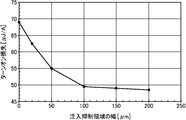
- FIG. 3A is a graph showing the relationship between the width of the injection suppression region 90 and the reverse recovery loss.
- the width of the injection suppression region 90 refers to the distance between the end portion of the transistor portion 70 and the end portion of the diode portion 80 in the arrangement direction (X-axis direction of FIGS. 1A to 2C).
- the width of the injection suppression region 90 is 0, it corresponds to the semiconductor device 1100 according to the comparative example, in which the injection suppression region 90 is not provided and the transistor portion 70 and the diode portion 80 are adjacent to each other.
- the reverse recovery loss decreases as the width of the injection suppression region 90 increases, and the reverse recovery loss decreases by about 36.5% when the width of the injection suppression region 90 increases from 0 to 200 ⁇ m. ..
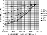
- FIG. 3B is a graph showing the relationship between the width of the injection suppression region 90 and the turn-on loss.
- the turn-on loss of the transistor portion 70 correlates with the reverse recovery loss because the reverse recovery current of the diode portion 80 of the opposite arm is added.
- increasing the width of the injection suppression region 90 from 0 to 200 ⁇ m reduces turn-on loss by 30.5%.
- FIG. 4A is a top view of the semiconductor device 100 according to the first embodiment of the present embodiment.
- FIG. 4A the positions where each member is projected onto the front surface 21 of the substrate 10 are shown. Note that FIG. 4A shows only a part of the members of the semiconductor device 100, and some members are omitted.
- the substrate 10 of the semiconductor device 100 has two sets of end sides 102 facing each other in a top view.
- the X-axis and the Y-axis are parallel to either end 102.
- the substrate 10 is provided with an active region 160.
- the active region 160 is a region in which the main current flows in the depth direction from the emitter region 12 of the substrate 10 when the semiconductor device 100 operates.
- the region surrounded by the gate runner 48 in the top view may be the active region 160.
- An emitter electrode is provided above the active region 160, but it is omitted in FIG. 4A.
- At least one of the transistor portion 70 and the diode portion 80 is provided in the active region 160.
- the transistor portion 70 and the diode portion 80 of this example are alternately arranged along a predetermined arrangement direction (X-axis direction in this example) on the front surface 21 of the substrate 10.
- the active region 160 may be provided with only one of the transistor portion 70 and the diode portion 80.
- the semiconductor device 100 may have one or more pads above the substrate 10.
- the semiconductor device 100 shown in FIG. 4A has a gate pad G in the active region 160.
- the gate pad G may be connected to an external circuit via wiring such as a wire.
- a gate potential is applied to the gate pad G.
- the gate pad G and the gate runner 48 are electrically connected, and the gate runner 48 surrounds the active region 160 and is electrically connected to the gate conductive portion of the gate trench portion 40 of the active region 160.
- the gate runner 48 is arranged between the active region 160 and the edge termination structure 190 of the substrate 10 in a top view.
- the gate runner 48 may be formed of a metal containing aluminum as a main component, such as polysilicon and an aluminum-silicon alloy.
- the semiconductor device 100 of this example includes an edge termination structure 190 between the active region 160 and the end side 102.
- the edge end structure portion 190 of this example is arranged between the gate runner 48 and the end side 102.
- the edge termination structure 190 relaxes the electric field concentration on the front surface 21 side of the substrate 10.
- the edge termination structure 190 may have a plurality of guard rings.
- the guard ring is a P-shaped region in contact with the front surface 21 of the substrate 10. By providing a plurality of guard rings, the depletion layer on the upper surface side of the active region 160 can be extended outward, and the withstand voltage of the semiconductor device 100 can be ensured.
- the edge termination structure 190 may further include at least one of a field plate and a resurf provided in an annular shape surrounding the gate runner 48.
- the semiconductor device 100 includes a temperature sense unit (not shown) which is a PN junction diode made of polysilicon or the like, and a current detection unit (not shown) which operates in the same manner as a transistor unit provided in the active region 160. You may.
- FIG. 4B is an enlarged view of part A of FIG. 4A.
- FIG. 4B shows an example in which one injection suppression region 90 is viewed from above (Z-axis positive side in FIG. 4B) to downward (Z-axis negative side).
- the injection suppression region 90 is also provided between the extension direction (Y-axis direction) end of the diode portion 80 and the outer circumference (gate runner 48) of the active region 160. That is, when viewed from above, the diode portion 80 is surrounded by the injection suppression region 90 at both the extension direction end portion and the arrangement direction (X-axis direction) end portion.
- the area of the substrate 10 is similarly expanded by S2.
- the diode does not increase the area of the substrate 10.
- the area S1 of the portion 80 may be reduced. Therefore, the ratio of the area S1 of the diode portion 80 may be 10% or more with respect to the total area (S1 + S2) of the diode portion 80 and the injection suppression region 90.
- the total area of the diode portion 80 may be 1.4% or more and 22% or less of the area of the semiconductor device 100 in top view.
- FIG. 4C is a graph showing the relationship between the width of the injection suppression region 90 and the reverse recovery loss.
- the solid line shows the reverse recovery loss when the area of the diode portion 80 is fixed and the area of the transistor portion 70 (that is, the width of the collector region 22) is reduced according to the increase in the width of the injection suppression region 90.
- the reverse recovery loss decreases by about 30%, whereas the area of the diode portion 80 is fixed. If so, the reduction in reverse recovery loss was only 21%. As described above, it can be seen that the reverse recovery loss is significantly reduced by 9% when the area of the diode portion 80 is reduced as compared with the case where the area of the diode portion 80 is fixed.
- FIG. 5A is a partial cross-sectional view of the semiconductor device 200 according to the second embodiment of the present embodiment.
- the same reference numerals are given to the elements common to the semiconductor device 100, and the description thereof will be omitted.
- the injection suppression region 90 of the semiconductor device 200 is provided with a second conductive type base region 94 instead of the base region 14.
- the doping concentration of the base region 94 may be 1 ⁇ e 16 cm -3 or more and 5 ⁇ e 19 cm -3 or less.
- the doping concentration of the base region 14 may be 1 ⁇ e 16 cm -3 or more and 1 ⁇ e 18 cm -3 or less, and the doping concentration of the extraction region 15 is 5 ⁇ e 18 cm -3 or more and 5 ⁇ e. It may be 20 cm -3 or less.
- the effect of suppressing hole injection from the transistor portion 70 can be enhanced. If the concentration of the base region 14 is lower than that of the base region 94, the effect of suppressing hole injection can be further enhanced.
- the processing method for separating the doping concentrations of the base region 14 and the base region 94 is as follows. If the doping concentration of the base region 94 is higher than the base region 14, both the base region 14 and 94 are doped, and then a mask is used for the base region 14 to open the base region 94 for doping. On the other hand, when the doping concentration of the base region 94 is lower than that of the base region 14, the base region 14 and the base region 94 are doped by using separate masks for processing.
- the same mask can be used for processing. Therefore, it is not necessary to add a mask, and it is possible to improve the workability and reduce the cost of the chip by reducing the mask.
- FIG. 5B is a graph showing the relationship between the doping concentration in the base region 94 of the injection suppression region 90 and the reverse recovery loss.
- boron is injected as an impurity.
- the width of the injection suppression region 90 is set in 7 patterns in the range of 10 ⁇ m to 250 ⁇ m, and the doping concentration of boron in the base region 94 is reduced from e 19 cm -3 order to e 16 cm -3 order in each pattern. , See the change in reverse recovery loss.
- the improvement width of the reverse recovery loss is 1.2% regardless of the width of any injection suppression region 90. , No big difference is seen.
- the doping concentration of the base region 94 is lowered from the reference concentration, the dependence on the width of the injection suppression region 90 increases, and the reverse recovery loss is significantly reduced.
- the reverse recovery loss is reduced by about 5.9% in the pattern in which the width of the injection suppression region 90 is 10 ⁇ m, and the reverse recovery loss at the reference concentration is reduced. There is no big difference. On the other hand, in the pattern in which the width of the injection suppression region 90 is 250 ⁇ m, the reverse recovery loss is significantly reduced to about 46%.
- FIG. 5C is a graph showing the relationship between the doping concentration in the base region 94 of the injection suppression region 90 and the turn-on loss. Since the setting of the width of the injection suppression region 90 is common to FIG. 5B, the description thereof will be omitted.
- FIG. 6A is a partial top view of the semiconductor device 300 according to the third embodiment of the present embodiment.
- the same reference numerals are given to the elements common to the semiconductor device 100, and the description thereof will be omitted.
- the injection suppression region 90 of the semiconductor device 300 has a dummy trench portion 30 and does not have a gate trench portion 40, similarly to the semiconductor devices 100 and 200. However, unlike the semiconductor devices 100 and 200, the injection suppression region 90 of the semiconductor device 300 has an emitter region 12 and a extraction region 15 exposed on the front surface 21. However, the ratio of the emitter region 12 and the extraction region 15 in the injection suppression region 90 is lower than the ratio of the emitter region 12 and the extraction region 15 in the transistor portion 70.
- the emitter region 12 and the extraction region 15 are smaller in the injection suppression region 90 than in the transistor portion 70. Further, in the injection suppression region 90, a base region 14 is provided in a portion where the emitter region 12 and the extraction region 15 are not provided.
- the emitter region 12 and the extraction region 15 are alternately arranged in the stretching direction (Y-axis direction in FIG. 6A), but in the injection suppression region 90, the extraction region 15 is arranged around the emitter region 12. , A base region 14 is provided around the base region 14.
- the injection suppression region 90 of the semiconductor devices 100 and 200 does not have the emitter region 12, no electron current flows from the emitter region 12, but in the semiconductor device 300, the injection suppression region 90 has the emitter region 12, so that the electrons Current flows. Therefore, the on-voltage can be reduced as compared with the semiconductor devices 100 and 200.
- FIG. 6B is an enlarged view of a portion B in FIG. 6A.
- the arrangement of the emitter region 12 and the extraction region 15 in the injection suppression region 90 will be mainly described.
- the mesa portion adjacent to the injection suppression region 90 is designated as the first mesa portion 60a, and among the mesa portions 60 of the injection suppression region 90, the mesa portion adjacent to the transistor portion 70
- the mesa portion adjacent to the second mesa portion 60b, the second mesa portion 60b is referred to as the third mesa portion 60c, and the mesa portion adjacent to the diode portion 80 is referred to as the fourth mesa portion 60d.
- the injection suppression region 90 of this example has three mesa portions, a second mesa portion 60b to a fourth mesa portion 60d, but the number of the mesa portions is not limited to this.
- either the emitter region 12 or the extraction region 15 is arranged so as to be adjacent to each of the emitter regions 12 arranged in the adjacent mesa portions on the negative side of the X axis. Will be done.
- first mesa portion 60a six emitter regions 12 and six extraction regions 15 are alternately arranged in the Y-axis direction. Of the six emitter regions 12 of the first mesa portion 60a, every other three emitter regions 12 are adjacent to the three emitter regions 12 arranged in the second mesa portion 60b, and the remaining three emitter regions 12 Is adjacent to each of the three extraction regions 15 arranged in the second mesa portion 60b.
- the three emitter regions 12 of the second mesa portion 60b are adjacent to the three emitter regions 12 of the third mesa portion 60c, respectively.
- the extraction region 15 may be arranged in the third mesa portion 60c instead of a part of the arranged three emitter regions 12.
- the emitter region 12 is adjacent to the extraction region 15 in the Y-axis direction. That is, the emitter region 12 is surrounded by the extraction region 15 on the positive and negative sides of the Y-axis. As a result, the holes generated by the conductivity modulation can be extracted to the extraction region 15, so that the latch-up resistance can be improved.
- the base region 14 is arranged in the region where the emitter region 12 and the extraction region 15 are not arranged.
- the emitter region 12 is not arranged in the fourth mesa portion 60d.
- a pull-out region 15 is arranged in the fourth mesa portion 60d, and is adjacent to the emitter region 12 of the third mesa portion 60c adjacent to each other on the negative side of the X-axis.
- the base region 14 is arranged in the region where the drawing region 15 is not arranged.
- the emitter region 12 is not arranged in the third mesa portion 60c adjacent to the fourth mesa portion 60d on the negative side of the X-axis, only the base region 14 may be arranged in the fourth mesa portion 60d.
- the ratio of the pull-out region 15 in each mesa portion of the injection suppression region 90 is less than or equal to the ratio of the pull-out region 15 in the adjacent mesa portion on the negative side of the X-axis. That is, the ratio of the pull-out region 15 in the second mesa portion 60b is equal to or less than the ratio of the pull-out region 15 in the first mesa portion 60a. The ratio of the pulled-out region 15 in the third mesa portion 60c is equal to or less than the ratio of the pulled-out region 15 in the second mesa portion 60b.
- the ratio of the drawn region 15 in the fourth mesa portion 60d is equal to or less than the ratio of the drawn region 15 in the third mesa portion 60c, and more than the ratio of the drawn region 15 in the mesa portion 61 of the adjacent diode portion 80 on the positive side of the X axis. Is.
- the number of the third mesa portions 60c may be increased. By increasing the number of the third mesa portions 60c, the ratio of the extraction region 15 in the injection suppression region 90 can be reduced, so that the reverse recovery loss and the turn-on loss can be reduced.
- the emitter region 12 is provided in the third mesa portion 60c, the area of the region that operates as the transistor portion is increased, and the on-voltage can be reduced.
- the extraction region 15 of the injection suppression region 90 is arranged over the entire mesa portion in the X-axis direction, but may be about half the length of the mesa portion in the X-axis direction. ..
- the length of the extraction region 15 in the X-axis direction may be 0.3 ⁇ m or more.
- the length of the extraction region 15 in the Y-axis direction is equal to or less than the length of the extraction region 15 of the transistor portion 70 in the Y-axis direction.
- the length of the extraction region 15 in the Y-axis direction may be 0.5 ⁇ m or more.
- a plug region 17 is arranged in the hatched portion of the contact hole 54 shown in FIG. 6B.
- FIG. 7A is a partial top view of the semiconductor device 400 according to the fourth embodiment of the present embodiment.
- FIG. 7B is a diagram showing a cross section taken along the line aa'in FIG. 7A.
- the same reference numerals are given to the elements common to the semiconductor device 100, and the description thereof will be omitted.
- the transistor portion 70 is provided with a plurality of gate trench portions 40 along the arrangement direction
- the diode portion 80 is provided with a plurality of dummy trench portions 30 along the arrangement direction.
- the transistor portion 70 of this example has a full gate structure in which the dummy trench portion 30 is not provided.
- Each of the gate trench portions 40 is connected to the adjacent gate trench portion 40 via the tip portion 41.
- FIG. 7C is a diagram for explaining the operation of the diode portion 80 of the semiconductor device 400 at the time of conduction.
- FIG. 7C shows a'a'cross section of FIG. 7A, similar to FIG. 7B.
- the same reference numerals are given to the elements common to the semiconductor device 100, and the description thereof will be omitted.
- FIG. 8A is a partial cross-sectional view of the semiconductor device 500 according to the fifth embodiment of the present embodiment.
- FIG. 8A is a diagram showing a'a'cross sections in FIGS. 8B and 8C described later.
- the aa'cross section is an XZ plane that includes a gate trench 40 and a dummy trench 30 and passes through a drawing region 15 and a base region 14.
- the same reference numerals are given to the elements common to the semiconductor device 100, and the description thereof will be omitted.
- the transistor portion 70 of this example has a gate trench portion 40 and a dummy trench portion 30 provided along the X-axis direction.
- the gate insulating film 42 and the dummy insulating film 32 are omitted.
- the injection suppression region 90 of this example has a gate trench portion 40 and a dummy trench portion 30 provided along the X-axis direction, unlike the semiconductor devices 100 to 400.
- the dummy ratio in the injection suppression region 90 is higher than the dummy ratio in the transistor portion 70.
- the dummy ratio means the ratio of the number of dummy trench portions 30 to the total number of gate trench portions 40 and dummy trench portions 30.
- one gate trench portion 40 and two dummy trench portions 30 are alternately arranged in the X-axis direction.
- the dummy ratio of such an arrangement is about 67%.
- one gate trench portion 40 and three dummy trench portions 30 are alternately arranged in the X-axis direction.
- the dummy ratio of such an arrangement is 75%.
- the diode portion 80 has a dummy trench portion 30 provided along the X-axis direction and does not have a gate trench portion 40. Therefore, the dummy ratio of the diode portion 80 is 100%.
- the dummy ratio of the diode portion 80 is higher than the dummy ratio of the injection suppression region 90, and the dummy ratio of the injection suppression region 90 is higher than the dummy ratio of the transistor portion 70.
- a dummy trench portion 30 is arranged at the boundary between the transistor portion 70 and the injection suppression region 90, but the present invention is not limited to this.
- a gate trench portion 40 may be arranged at the boundary between the transistor portion 70 and the injection suppression region 90.
- a dummy trench portion 30 may be arranged at the boundary between the injection suppression region 90 and the diode portion 80.
- the plug is provided in the contact hole in contact with the drawing region 15 or the base region 14. Further, under the contact hole of the plug, a P ++ type plug region 17 having a doping concentration higher than that of the withdrawal region 15 is formed.
- FIG. 8B is a partial top view of the semiconductor device 500.
- FIG. 8B shows the transistor portion 70 at the center.
- the transistor portion 70 of this example has a gate trench portion 40 and a dummy trench portion 30 provided along the X-axis direction.
- the straight portion 29 of the two dummy trench portions 30 is arranged between the straight portions 39 of the two gate trench portions 40.
- the tip 41 connects the ends of the two straight portions 39 in the Y-axis direction to the gate runner 48.
- the dummy ratio of the transistor unit 70 is 0% or more and 75% or less.
- the ratio of the number of gate trench portions 40 to the number of dummy trench portions 30 may be 1: 0 (so-called full gate structure), and 1: 1 (one gate trench portion 40 and one).
- the dummy trench portions 30 of the above may be arranged alternately in the X-axis direction), and 1: 2 (one gate trench portion 40 and two dummy trench portions 30 are alternately arranged in the X-axis direction). It may be a structure in which it is arranged), and it may be 1: 3 (a structure in which one gate trench portion 40 and three dummy trench portions 30 are alternately arranged in the X-axis direction).
- FIG. 8C is a partial top view of the semiconductor device 500.
- FIG. 8C shows the injection suppression region 90 as the center.
- the injection suppression region 90 of this example has a gate trench portion 40 and a dummy trench portion 30 provided along the X-axis direction.
- the straight portions 29 of the three dummy trench portions 30 are arranged between the straight portions 39 of the two gate trench portions 40.
- the tip 41 connects the ends of the two straight portions 39 in the Y-axis direction to the gate runner 48.
- the emitter region 12 is arranged in the mesa portion 60 adjacent to the gate trench portion 40. Further, in the injection suppression region 90, the emitter region 12 and the extraction region 15 are alternately arranged in the Y-axis direction.
- the base region 14 is arranged in the portion where the emitter region 12 and the extraction region 15 are not arranged. That is, in the injection suppression region 90, the emitter region 12 and the extraction region 15 are not arranged in the mesa portion 60 adjacent to the dummy trench portion 30, but the base region 14 is arranged.
- the dummy ratio of the injection suppression region 90 is higher than that of the transistor portion 70, and the emitter region 12 and the extraction region 15 are arranged in the mesa portion 60 adjacent to the gate trench portion 40. Therefore, the ratio of the emitter region 12 and the extraction region 15 in the injection suppression region 90 is lower than that of the transistor portion 70. This suppresses hole injection and improves reverse recovery loss.
- the injection suppression region 90 since the injection suppression region 90 has an emitter region 12, an electron current flows. As a result, the injection suppression region 90 partially performs the transistor operation, and the deterioration of the on-voltage can be suppressed.
- the emitter region 12 is surrounded by the extraction region 15 on the positive side and the negative side of the Y axis. As a result, the holes generated by the conductivity modulation can be extracted to the extraction region 15, so that the latch-up resistance can be improved.
- the dummy ratio of the injection suppression region 90 is 75% or more and 87.5% or less.
- the ratio of the number of gate trench portions 40 to the number of dummy trench portions 30 is 1: 3 (one gate trench portion 40 and three dummy trench portions 30 alternate in the X-axis direction. It may be 1: 4 (a structure in which one gate trench portion 40 and four dummy trench portions 30 are alternately arranged in the X-axis direction). It may be 5 (a structure in which one gate trench portion 40 and five dummy trench portions and 30 are alternately arranged in the X-axis direction), and 1: 6 (one gate trench portion 40 and six).
- the structure may be such that the dummy trench portions 30 are alternately arranged in the X-axis direction), and 1: 7 (one gate trench portion 40 and seven dummy trench portions 30 are alternately arranged in the X-axis direction).
- the structure to be used) may be used.
- FIG. 8D is a partial top view of the semiconductor device 500.
- FIG. 8D shows the injection suppression region 90 as the center, as in FIG. 8C.
- FIG. 8D shows variations in the arrangement of the gate trench portion 40 and the dummy trench portion 30 in the injection suppression region 90. The description of the configuration common to FIG. 8C will be omitted.
- the straight portions 29 of the seven dummy trench portions 30 are arranged between the straight portions 39 of the two gate trench portions 40.
- the tip 41 connects the ends of the two straight portions 39 in the Y-axis direction to the gate runner 48.
- one gate trench portion 40 and seven dummy trench portions 30 are alternately arranged in the X-axis direction.
- the dummy ratio of such an arrangement is 87.5%.
- FIG. 8C shows an arrangement in which the dummy ratio of the injection suppression region 90 is minimized (a structure in which one gate trench portion 40 and three dummy trench portions 30 are alternately arranged in the X-axis direction).
- FIG. 8D shows an arrangement in which the dummy ratio of the injection suppression region 90 is maximized (a structure in which one gate trench portion 40 and seven dummy trench portions 30 are alternately arranged in the X-axis direction).
- the dummy ratio of the injection suppression region 90 is set higher than that of the transistor portion 70, and the injection suppression region 90 is turned on by partially performing the transistor operation by setting the dummy ratio in the range shown in FIGS. 8C to 8D. It is possible to suppress hole injection and improve reverse recovery loss while suppressing voltage deterioration.
Landscapes
- Engineering & Computer Science (AREA)
- Power Engineering (AREA)
- Microelectronics & Electronic Packaging (AREA)
- Physics & Mathematics (AREA)
- Condensed Matter Physics & Semiconductors (AREA)
- General Physics & Mathematics (AREA)
- Computer Hardware Design (AREA)
- Ceramic Engineering (AREA)
- Manufacturing & Machinery (AREA)
- Metal-Oxide And Bipolar Metal-Oxide Semiconductor Integrated Circuits (AREA)
Abstract
トランジスタ部とダイオード部とを有する半導体基板を備え、トランジスタ部は、半導体基板の上面視でダイオード部側の端部において、第2導電型キャリアの注入を抑制する注入抑制領域を有する半導体装置を提供する。トランジスタ部及びダイオード部の双方が、半導体基板のおもて面に第2導電型のベース領域を有し、トランジスタ部は、半導体基板のおもて面に、第1導電型のエミッタ領域と、ベース領域よりドーピング濃度が高い第2導電型の引き抜き領域とをさらに有し、注入抑制領域には、エミッタ領域及び引き抜き領域が設けられていない。
Description
本発明は、半導体装置に関する。
従来、絶縁ゲート型バイポーラトランジスタ(IGBT)等のトランジスタ部と、ダイオード部とを同一基板に形成した半導体装置において、ダイオード部のアノード層よりも不純物濃度の高いコンタクト層をトランジスタ部に設けることが知られている(例えば、特許文献1)。
特許文献1 国際公開第2016/030966号公報
特許文献1 国際公開第2016/030966号公報
このような半導体装置では、ダイオード部の還流時、アノード層から正孔が供給されるだけでなく、カソード層からの電子電流がトランジスタ部側に流入し、コンタクト層からも正孔が注入される。そのため逆回復電流が増加し、インバータ損失が大きくなる。
本発明の第1の態様においては、半導体装置を提供する。半導体装置は、トランジスタ部とダイオード部とを有する半導体基板を備え、トランジスタ部は、半導体基板の上面視でダイオード部側の端部において、第2導電型キャリアの注入を抑制する注入抑制領域を有する。
トランジスタ部及びダイオード部の双方が、半導体基板のおもて面に第2導電型のベース領域を有し、トランジスタ部は、半導体基板のおもて面に、第1導電型のエミッタ領域と、ベース領域よりドーピング濃度が高い第2導電型の引き抜き領域とをさらに有し、注入抑制領域には、エミッタ領域及び引き抜き領域が設けられていなくてよい。
半導体基板の上面視で、トランジスタ部及びダイオード部の配列方向における注入抑制領域の幅は、20μm以上、900μm以下であってよい。
半導体基板の上面視で、ダイオード部の延伸方向における端部と活性領域の外周との間に注入抑制領域がさらに設けられてよい。
半導体基板の上面視で、ダイオード部の面積は、ダイオード部及び注入抑制領域の合計面積の10%以上であってよい。
半導体基板の上面視で、ダイオード部の総面積は、半導体装置の面積の1.4%以上、22%以下であってよい。
注入抑制領域におけるベース領域のドーピング濃度は、ダイオード部のベース領域のドーピング濃度以下であってよい。
注入抑制領域におけるベース領域のドーピング濃度は、1×e16cm-3以上、5×e19cm-3以下であってよい。
ダイオード部のベース領域のドーピング濃度は、1×e16cm-3以上、1×e18cm-3以下であってよい。
引き抜き領域のドーピング濃度は、5×e18cm-3以上、5×e20cm-3以下であってよい。
トランジスタ部及びダイオード部の双方が、半導体基板のおもて面に第2導電型のベース領域を有し、トランジスタ部及び注入抑制領域は、半導体基板のおもて面に、第1導電型のエミッタ領域と、ベース領域よりドーピング濃度が高い第2導電型の引き抜き領域とをさらに有し、半導体基板の上面視で、注入抑制領域におけるエミッタ領域及び引き抜き領域の比率は、トランジスタ部におけるエミッタ領域及び引き抜き領域の比率より低くてよい。
トランジスタ部及び注入抑制領域は、トランジスタ部及びダイオード部の延伸方向に延伸し、トランジスタ部及びダイオード部の配列方向に配列される複数のトレンチ部の間に、延伸方向に延伸する複数のメサ部を有し、注入抑制領域のメサ部には、エミッタ領域又は引き抜き領域のいずれかが、トランジスタ部側に隣接するメサ部に配置されたエミッタ領域のそれぞれと隣接するように配置されてよい。
複数のトレンチ部は、ゲートトレンチ部およびダミートレンチ部を含み、注入抑制領域は、ダミートレンチ部を有し、ゲートトレンチ部を有さなくてよい。
複数のトレンチ部は、ゲートトレンチ部およびダミートレンチ部を含み、注入抑制領域における、ゲートトレンチ部およびダミートレンチ部の総数に対するダミートレンチ部の数の比率であるダミー比率は、注入抑制領域を除くトランジスタ部におけるダミー比率より高くてよい。
注入抑制領域のエミッタ領域は、ゲートトレンチ部に隣接するメサ部に配置されてよい。
注入抑制領域におけるダミー比率は、75%以上、87.5%以下であってよい。
注入抑制領域を除くトランジスタ部におけるダミー比率は、0%以上、75%以下であってよい。
注入抑制領域のエミッタ領域は、延伸方向において引き抜き領域と隣接してよい。
注入抑制領域においてダイオード部に隣接するメサ部には、エミッタ領域が配置されていなくてよい。
半導体基板の上面視で、トランジスタ部及びダイオード部の延伸方向において、引き抜き領域の長さは0.5μm以上であってよい。
半導体基板の上面視で、トランジスタ部及びダイオード部の配列方向において、引き抜き領域の長さは0.3μm以上であってよい。
注入抑制領域において、エミッタ領域及び引き抜き領域が配置されていない部分にベース領域が配置されていてよい。
半導体基板の内部において、第1導電型の蓄積領域をさらに有してよい。
なお、上記の発明の概要は、本発明の必要な特徴の全てを列挙したものではない。また、これらの特徴群のサブコンビネーションもまた、発明となりうる。
以下、発明の実施の形態を通じて本発明を説明するが、以下の実施形態は請求の範囲にかかる発明を限定するものではない。また、実施形態の中で説明されている特徴の組み合わせの全てが発明の解決手段に必須であるとは限らない。
本明細書においては半導体基板の深さ方向と平行な方向における一方の側を「上」、他方の側を「下」と称する。基板、層又はその他の部材の2つの主面のうち、一方の面をおもて面、他方の面を裏面と称する。「上」、「下」の方向は、重力方向又は半導体装置の実装時における方向に限定されない。
本明細書では、X軸、Y軸及びZ軸の直交座標軸を用いて技術的事項を説明する場合がある。直交座標軸は、構成要素の相対位置を特定するに過ぎず、特定の方向を限定するものではない。例えば、Z軸は地面に対する高さ方向を限定して示すものではない。なお、+Z軸方向と-Z軸方向とは互いに逆向きの方向である。正負を記載せず、Z軸方向と記載した場合、+Z軸及びZ軸に平行な方向を意味する。
本明細書では、半導体基板のおもて面及び裏面に平行な直交軸をX軸及びY軸とする。また、半導体基板のおもて面及び裏面と垂直な軸をZ軸とする。本明細書では、Z軸の方向を深さ方向と称する場合がある。また、本明細書では、X軸及びY軸を含めて、半導体基板のおもて面及び裏面に平行な方向を、水平方向と称する場合がある。
本明細書において「同一」又は「等しい」のように称した場合、製造ばらつき等に起因する誤差を有する場合も含んでよい。当該誤差は、例えば10%以内である。
本明細書においては、不純物がドーピングされたドーピング領域の導電型をP型又はN型として説明している。本明細書においては、不純物とは、特にN型のドナー又はP型のアクセプタの何れかを意味する場合があり、ドーパントと記載する場合がある。本明細書においては、ドーピングとは、半導体基板にドナー又はアクセプタを導入し、N型の導電型を示す半導体又はP型の導電型を示す半導体とすることを意味する。
本明細書においては、ドーピング濃度とは、熱平衡状態におけるドナーの濃度又はアクセプタの濃度を意味する。本明細書においては、ネット・ドーピング濃度とは、ドナー濃度を正イオンの濃度とし、アクセプタ濃度を負イオンの濃度として、電荷の極性を含めて足し合わせた正味の濃度を意味する。一例として、ドナー濃度をND、アクセプタ濃度をNAとすると、任意の位置における正味のネット・ドーピング濃度はND-NAとなる。
ドナーは、半導体に電子を供給する機能を有している。アクセプタは、半導体から電子を受け取る機能を有している。ドナー及びアクセプタは、不純物自体には限定されない。例えば、半導体中に存在する空孔(V)、酸素(O)及び水素(H)が結合したVOH欠陥は、電子を供給するドナーとして機能する。
本明細書においてP+型又はN+型と記載した場合、P型又はN型よりもドーピング濃度が高いことを意味し、P-型又はN-型と記載した場合、P型又はN型よりもドーピング濃度が低いことを意味する。また、本明細書においてP++型又はN++型と記載した場合には、P+型又はN+型よりもドーピング濃度が高いことを意味する。
本明細書において化学濃度とは、電気的な活性化の状態によらずに測定される不純物の濃度を指す。化学濃度は、例えば二次イオン質量分析法(SIMS)により計測できる。上述したネット・ドーピング濃度は、電圧-容量測定法(CV法)により測定できる。また、拡がり抵抗測定法(SR法)により計測されるキャリア濃度を、ネット・ドーピング濃度としてよい。CV法又はSR法により計測されるキャリア濃度は、熱平衡状態における値としてよい。また、N型の領域においては、ドナー濃度がアクセプタ濃度よりも十分大きいので、当該領域におけるキャリア濃度を、ドナー濃度としてもよい。同様に、P型の領域においては、当該領域におけるキャリア濃度を、アクセプタ濃度としてもよい。
また、ドナー、アクセプタ又はネット・ドーピングの濃度分布がピークを有する場合、当該ピーク値を当該領域におけるドナー、アクセプタ又はネット・ドーピングの濃度としてよい。ドナー、アクセプタ又はネット・ドーピングの濃度がほぼ均一な場合等においては、当該領域におけるドナー、アクセプタ又はネット・ドーピングの濃度の平均値をドナー、アクセプタ又はネット・ドーピングの濃度としてよい。
SR法により計測されるキャリア濃度が、ドナー又はアクセプタの濃度より低くてもよい。拡がり抵抗を測定する際に電流が流れる範囲において、半導体基板のキャリア移動度が結晶状態の値よりも低い場合がある。キャリア移動度の低下は、格子欠陥等による結晶構造の乱れ(ディスオーダー)により、キャリアが散乱されることで生じる。
CV法又はSR法により計測されるキャリア濃度から算出したドナー又はアクセプタの濃度は、ドナー又はアクセプタを示す元素の化学濃度よりも低くてよい。一例として、シリコンの半導体においてドナーとなるリン又はヒ素のドナー濃度、あるいはアクセプタとなるボロン(ホウ素)のアクセプタ濃度は、これらの化学濃度の99%程度である。一方、シリコンの半導体においてドナーとなる水素のドナー濃度は、水素の化学濃度の0.1%から10%程度である。
[実施例1]
図1Aは、本実施形態の実施例1に係る半導体装置100の部分上面図である。半導体装置100は、IGBT等のトランジスタ素子を含むトランジスタ部70と、還流ダイオード(FWD)等のダイオード素子を含むダイオード部80とを有する半導体基板を備える。
図1Aは、本実施形態の実施例1に係る半導体装置100の部分上面図である。半導体装置100は、IGBT等のトランジスタ素子を含むトランジスタ部70と、還流ダイオード(FWD)等のダイオード素子を含むダイオード部80とを有する半導体基板を備える。
なお、本明細書で単に上面視と称した場合、半導体基板のおもて面側から見ることを意味している。本例では、上面視でトランジスタ部70及びダイオード部80の配列方向をX軸、半導体基板のおもて面においてX軸と垂直な方向をY軸、半導体基板のおもて面と垂直な方向をZ軸と称する。
トランジスタ部70及びダイオード部80は、それぞれ延伸方向に長手を有してよい。つまり、トランジスタ部70のY軸方向における長さは、X軸方向における幅よりも大きい。同様に、ダイオード部80のY軸方向における長さは、X軸方向における幅よりも大きい。トランジスタ部70及びダイオード部80の延伸方向と、後述する各トレンチ部の長手方向とは同一であってよい。
ダイオード部80は、半導体基板の裏面と接する領域に、N+型のカソード領域を有する。本明細書では、カソード領域が設けられた領域を、ダイオード部80と称する。つまりダイオード部80は、上面視においてカソード領域と重なる領域である。一方、トランジスタ部70は、半導体基板の裏面と接する領域に、P+型のコレクタ領域を有する。
本例の半導体装置100は、半導体基板のおもて面側の内部に設けられたゲートトレンチ部40、ダミートレンチ部30、ウェル領域11、エミッタ領域12、ベース領域14及び引き抜き領域15を備える。ゲートトレンチ部40及びダミートレンチ部30は、それぞれがトレンチ部の一例である。
また、本例の半導体装置100は、半導体基板のおもて面の上方に設けられたゲート金属層50及びエミッタ電極52を備える。ゲート金属層50及びエミッタ電極52は、互いに分離して設けられる。
エミッタ電極52及びゲート金属層50と、半導体基板のおもて面との間には層間絶縁膜が設けられるが、図1Aでは省略している。本例の層間絶縁膜には、コンタクトホール49、54、56及び58が、当該層間絶縁膜を貫通して設けられる。図1Aにおいては、それぞれのコンタクトホールに斜線のハッチングを付している。
エミッタ電極52は、ゲートトレンチ部40、ダミートレンチ部30、ウェル領域11、エミッタ領域12、ベース領域14及び引き抜き領域15の上方に設けられる。エミッタ電極52は、コンタクトホール54を通って、半導体基板のおもて面におけるエミッタ領域12、ベース領域14及び引き抜き領域15と接触する。
また、エミッタ電極52は、コンタクトホール56又はコンタクトホール58を通ってダミートレンチ部30内のダミー導電部と接続される。エミッタ電極52とダミー導電部との間には、不純物がドープされたポリシリコン等の、導電性を有する材料で形成された接続部25が設けられてよい。接続部25は、それぞれ絶縁膜を介して半導体基板のおもて面に設けられる。
ゲート金属層50は、コンタクトホール49を通ってゲートランナー48と接触する。ゲートランナー48は、不純物がドープされたポリシリコン等で形成されてよい。ゲートランナー48は、半導体基板のおもて面において、ゲートトレンチ部40内のゲート導電部に接続する。ゲートランナー48は、ダミートレンチ部30内のダミー導電部およびエミッタ電極52には電気的に接続しない。
ゲートランナー48とエミッタ電極52とは層間絶縁膜及び酸化膜などの絶縁物により電気的に分離されてよい。本例のゲートランナー48は、コンタクトホール49の下方から、ゲートトレンチ部40の先端部まで設けられる。ゲートトレンチ部40の先端部においてゲート導電部は半導体基板のおもて面に露出しており、ゲートランナー48と接触する。
エミッタ電極52及びゲート金属層50は、金属を含む導電性材料で形成される。例えば、ポリシリコン及びアルミニウム又はアルミニウム-シリコン合金で形成される。各電極は、アルミニウム等で形成された領域の下層にチタンやチタン化合物等で形成されたバリアメタルを有してよい。
各電極は、コンタクトホール内においてタングステン等で形成されたプラグを有してもよい。プラグは、半導体基板に接する側にバリアメタルを有し、バリアメタルに接するようにタングステンを埋め込み、タングステン上にアルミニウム等で形成されてよい。
なおプラグは、引き抜き領域15又はベース領域14に接するコンタクトホールに設けられる。また、プラグのコンタクトホールの下には、引き抜き領域15よりドーピング濃度が高いP++型のプラグ領域17を形成する。これは、バリアメタルと引き抜き領域15との接触抵抗を改善することができる。また、プラグ領域17の深さは約0.1μm以下であり、引き抜き領域15の深さと比べて10%以下と小さい領域を持つ。
プラグ領域17は以下の特徴をもつ。トランジスタ部70の動作において、接触抵抗改善によりラッチアップ耐量が向上する。一方、ダイオード部80の動作においては、プラグ領域がない場合はバリアメタルとベース領域14との接触抵抗が高く、導通損失、スイッチング損失が上昇するが、プラグ領域17を設けることにより、導通損失、スイッチング損失の上昇を抑制することができる。
ウェル領域11は、ゲートランナー48と重なって設けられている。ウェル領域11は、ゲートランナー48と重ならない範囲にも、所定の幅で延伸して設けられている。本例のウェル領域11は、コンタクトホール54のY軸方向の端から、ゲートランナー48側に離れて設けられている。ウェル領域11は、ベース領域14よりもドーピング濃度の高い第2導電型の領域である。
本例のベース領域14はP-型であり、ウェル領域11はP+型である。また、ウェル領域11は、半導体基板のおもて面から、ベース領域14の下端よりも深い位置まで形成されている。
トランジスタ部70及びダイオード部80のそれぞれは、配列方向に複数配列されたトレンチ部を有する。本例のトランジスタ部70には、配列方向に沿って1以上のゲートトレンチ部40と、1以上のダミートレンチ部30とが交互に設けられている。本例のダイオード部80には、複数のダミートレンチ部30が、配列方向に沿って設けられている。本例のダイオード部80には、ゲートトレンチ部40が設けられていない。
本例のゲートトレンチ部40は、配列方向と垂直な延伸方向に沿って延伸する2つの直線部分39(延伸方向に沿って直線状であるトレンチの部分)と、2つの直線部分39を接続する先端部41を有してよい。
先端部41の少なくとも一部は、上面視において曲線状に設けられてよい。2つの直線部分39のY軸方向における端部同士を先端部41がゲートランナー48と接続することで、ゲートトレンチ部40へのゲート電極として機能する。一方、先端部41を曲線状にすることにより直線部分39で完結するよりも端部におけるゲートバイアス時の電界集中を緩和できる。
トランジスタ部70において、ダミートレンチ部30はゲートトレンチ部40のそれぞれの直線部分39の間に設けられる。それぞれの直線部分39の間には、1本のダミートレンチ部30が設けられてよく、複数本のダミートレンチ部30が設けられていてもよい。
またそれぞれの直線部分39の間には、ダミートレンチ部30が設けられなくてもよく、ゲートトレンチ部40が設けられてもよい。このような構造により、エミッタ領域12からの電子電流を増大することができるため、オン電圧が低減する。
ダミートレンチ部30は、延伸方向に延伸する直線形状を有してよく、ゲートトレンチ部40と同様に、直線部分29と先端部31とを有していてもよい。図1Aに示した半導体装置100は、先端部31を有さない直線形状のダミートレンチ部30と、先端部31を有するダミートレンチ部30の両方を含んでいる。
ウェル領域11の拡散深さは、ゲートトレンチ部40及びダミートレンチ部30の深さよりも深くてよい。ゲートトレンチ部40及びダミートレンチ部30のY軸方向の端部は、上面視においてウェル領域11に設けられる。つまり、各トレンチ部のY軸方向の端部において、各トレンチ部の深さ方向の底部は、ウェル領域11に覆われている。これにより、各トレンチ部の当該底部における電界集中を緩和できる。
配列方向において各トレンチ部の間には、メサ部が設けられている。メサ部は、半導体基板の内部において、トレンチ部に挟まれた領域を指す。一例としてメサ部の深さ位置は、半導体基板のおもて面からトレンチ部の下端までである。
本例のメサ部は、X軸方向において隣接するトレンチ部に挟まれ、半導体基板のおもて面においてトレンチに沿って延伸方向(Y軸方向)に延伸して設けられている。図1Bで後述するように、本例では、トランジスタ部70にはメサ部60が設けられ、ダイオード部80にはメサ部61が設けられている。本明細書において単にメサ部と称した場合、メサ部60及びメサ部61のそれぞれを指している。
それぞれのメサ部には、ベース領域14が設けられる。トランジスタ部70のそれぞれのメサ部には、上面視においてベース領域14に挟まれた領域に、第1導電型のエミッタ領域12及び第2導電型の引き抜き領域15の少なくとも一方が設けられてよい。本例のエミッタ領域12はN+型であり、引き抜き領域15はP+型である。エミッタ領域12及び引き抜き領域15は、深さ方向において、ベース領域14と半導体基板のおもて面との間に設けられてよい。
トランジスタ部70のメサ部は、半導体基板のおもて面に露出したエミッタ領域12を有する。エミッタ領域12は、ゲートトレンチ部40に接して設けられている。ゲートトレンチ部40に接するメサ部には、半導体基板のおもて面に露出した引き抜き領域15が設けられている。
メサ部における引き抜き領域15及びエミッタ領域12のそれぞれは、X軸方向における一方のトレンチ部から、他方のトレンチ部まで設けられる。一例として、メサ部の引き抜き領域15及びエミッタ領域12は、トレンチ部の延伸方向(Y軸方向)に沿って交互に配置されている。
他の例においては、メサ部の引き抜き領域15及びエミッタ領域12は、トレンチ部の延伸方向(Y軸方向)に沿ってストライプ状に設けられていてもよい。例えばトレンチ部に接する領域にエミッタ領域12が設けられ、エミッタ領域12に挟まれた領域に引き抜き領域15が設けられる。
ただし、トランジスタ部70において、後述する注入抑制領域90に隣接するメサ部には、エミッタ領域12が設けられておらず、半導体基板のおもて面に露出した引き抜き領域15が設けられる。引き抜き領域15は、上面視においてベース領域14に挟まれた領域に、ダミートレンチ部30に接して設けられてよい。
ダイオード部80のメサ部には、エミッタ領域12が設けられていない。ダイオード部80のメサ部の上面には、ベース領域14が設けられてよい。ベース領域14は、ダイオード部80のメサ部全体に配置されてよい。
それぞれのメサ部の上方には、コンタクトホール54が設けられている。コンタクトホール54は、その延伸方向(Y軸方向)においてベース領域14に挟まれた領域に配置されている。本例のコンタクトホール54は、引き抜き領域15、ベース領域14及びエミッタ領域12の各領域の上方に設けられる。コンタクトホール54は、メサ部の配列方向(X軸方向)における中央に配置されてよい。
ダイオード部80において、半導体基板の裏面と隣接する領域には、N+型のカソード領域82が設けられる。半導体基板の裏面において、カソード領域82が設けられていない領域には、P+型のコレクタ領域22が設けられてよい。図1Aにおいては、カソード領域82及びコレクタ領域22の境界を点線で示している。
カソード領域82は、Y軸方向においてウェル領域11から離れて配置されている。これにより、比較的にドーピング濃度が高く、且つ、深い位置まで形成されているP型の領域(ウェル領域11)と、カソード領域82との距離を確保することにより、ウェル領域11からのホール注入を抑制できるため、逆回復損失を低減できる。本例のカソード領域82のY軸方向における端部は、コンタクトホール54のY軸方向における端部よりも、ウェル領域11から離れて配置されている。他の例では、カソード領域82のY軸方向における端部は、ウェル領域11とコンタクトホール54との間に配置されていてもよい。
トランジスタ部70は、半導体基板の上面視でダイオード部80側の端部において、第2導電型キャリアの注入を抑制する注入抑制領域90を有する。
注入抑制領域90において、半導体基板の裏面にはP+型のコレクタ領域22が設けられている。すなわち、注入抑制領域90はトランジスタ部70の一部であるが、本明細書においては、基本的にはトランジスタ部70と注入抑制領域90とを区別して説明する。
注入抑制領域90の上面には、トランジスタ部70と異なり、エミッタ領域12及び引き抜き領域15が設けられておらず、ベース領域14が設けられている。また、注入抑制領域90は、トランジスタ部70と異なり、ゲートトレンチ部40を有さず、ダミートレンチ部30を有する。
なお、図1Aにおいて、注入抑制領域90はダミートレンチ部30から隣接する2つのメサ部として示されているが、これに限られない。注入抑制領域90は、2より多くのメサ部を有してもよい。
図1Bは、図1Aにおけるa-a'断面を示す図である。a-a'断面は、エミッタ領域12、ベース領域14、並びにゲートトレンチ部40及びダミートレンチ部30を通るXZ面である。本例の半導体装置100は、a-a'断面において、基板10、層間絶縁膜38、エミッタ電極52及びコレクタ電極24を有する。
層間絶縁膜38は、基板10のおもて面21に設けられている。層間絶縁膜38は、ボロン又はリン等の不純物が添加されたシリケートガラス等の絶縁膜である。層間絶縁膜38はおもて面21に接していてよく、層間絶縁膜38とおもて面21との間に酸化膜等の他の膜が設けられていてもよい。層間絶縁膜38には、図1Aにおいて説明したコンタクトホール54が設けられている。
エミッタ電極52は、基板10のおもて面21及び層間絶縁膜38の上面に設けられる。エミッタ電極52は、層間絶縁膜38のコンタクトホール54を通って、おもて面21と電気的に接触する。コンタクトホール54の内部には、タングステン(W)等のコンタクトプラグが設けられてもよい。コレクタ電極24は、基板10の裏面23に設けられる。エミッタ電極52及びコレクタ電極24は、金属を含む材料で形成される。
基板10は、シリコン基板であってよく、炭化シリコン基板であってよく、窒化ガリウム等の窒化物半導体基板等であってもよい。本例の基板10はシリコン基板である。
基板10は、第1導電型のドリフト領域18を有する。本例のドリフト領域18は、N-型である。ドリフト領域18は、基板10において他のドーピング領域が設けられずに残存した領域であってよい。
ドリフト領域18の上方には、Z軸方向に一つ以上の蓄積領域16が設けられてよい。蓄積領域16は、ドリフト領域18と同じドーパントが、ドリフト領域18よりも高濃度に蓄積した領域である。蓄積領域16のドーピング濃度は、ドリフト領域18のドーピング濃度よりも高い。蓄積領域16を設けることで、キャリアの注入促進効果(IE効果)を高めて、オン電圧を低減できる。
トランジスタ部70において、ベース領域14の上方には、おもて面21に接してエミッタ領域12が設けられる。エミッタ領域12は、ゲートトレンチ部40と接して設けられる。エミッタ領域12のドーピング濃度は、ドリフト領域18のドーピング濃度よりも高い。エミッタ領域12のドーパントは、一例としてヒ素(As)、リン(P)、アンチモン(Sb)等である。
注入抑制領域90の配列方向(図1BにおけるX軸方向)における幅Aは、20μm以上、900μm以下である。また注入抑制領域90の幅Aと半導体装置100の基板厚さWとの間には、以下の式(1)が成り立つ。
A≦6W・・・[式(1)]
A≦6W・・・[式(1)]
なお、基板厚さWは、ダイオード部80のベース領域14の上面からカソード領域82の下面までの厚さを示す。基板厚さWが増すことにより、ダイオード部80のカソード領域82の電子の拡散領域が増加するため、式(1)より、逆回復及びターンオン損失を低減することがわかる。
またトランジスタ部70において、注入抑制領域90側のメサ部60には、ベース領域14の上方に、おもて面21に接して引き抜き領域15が設けられる。引き抜き領域15は、ダミートレンチ部30に接して設けられてよい。
ダイオード部80及び注入抑制領域90には、おもて面21に露出したベース領域14が設けられる。ダイオード部80のベース領域14は、アノードとして動作する。
ドリフト領域18の下方には、第1導電型のバッファ領域20が設けられてよい。本例のバッファ領域20は、N型である。バッファ領域20のドーピング濃度は、ドリフト領域18のドーピング濃度よりも高い。バッファ領域20は、ベース領域14の下面側から広がる空乏層が、コレクタ領域22及びカソード領域82に到達することを防ぐフィールドストップ層として機能してよい。
トランジスタ部70及び注入抑制領域90において、バッファ領域20の下方にはコレクタ領域22が設けられる。注入抑制領域90のコレクタ領域22は、裏面23においてカソード領域82と接して設けられていてよい。
ダイオード部80において、バッファ領域20の下方にはカソード領域82が設けられる。カソード領域82は、トランジスタ部70及び注入抑制領域90のコレクタ領域22と同じ深さに設けられてよい。ダイオード部80は、トランジスタ部70がターンオフする時に、逆方向に導通する還流電流を流す還流ダイオード(FWD)として機能してよい。
基板10には、ゲートトレンチ部40及びダミートレンチ部30が設けられる。ゲートトレンチ部40及びダミートレンチ部30は、おもて面21からベース領域14及び蓄積領域16を貫通して、ドリフト領域18に到達するように設けられる。トレンチ部がドーピング領域を貫通するとは、ドーピング領域を形成してからトレンチ部を形成する順序で製造したものに限定されない。トレンチ部を形成した後に、トレンチ部の間にドーピング領域を形成したものも、トレンチ部がドーピング領域を貫通しているものに含まれる。
ゲートトレンチ部40は、おもて面21に設けられたゲートトレンチ、ゲート絶縁膜42及びゲート導電部44を有する。ゲート絶縁膜42は、ゲートトレンチの内壁を覆って設けられる。ゲート絶縁膜42は、ゲートトレンチの内壁の半導体を酸化又は窒化して形成してよい。ゲート導電部44は、ゲートトレンチの内部においてゲート絶縁膜42よりも内側に設けられる。ゲート導電部44の上面は、おもて面21と同じXY平面内にあってよい。ゲート絶縁膜42は、ゲート導電部44と基板10とを絶縁する。ゲート導電部44は、不純物がドープされたポリシリコン等の半導体で形成される。
ゲート導電部44は、深さ方向においてベース領域14よりも長く設けられてよい。ゲートトレンチ部40は、おもて面21において層間絶縁膜38により覆われる。ゲート導電部44に所定の電圧が印加されると、ベース領域14のうちゲートトレンチに接する界面の表層に、電子の反転層によるチャネルが形成される。
ダミートレンチ部30は、XZ断面においてゲートトレンチ部40と同一の構造を有してよい。ダミートレンチ部30は、おもて面21に設けられたダミートレンチ、ダミー絶縁膜32及びダミー導電部34を有する。ダミー絶縁膜32は、ダミートレンチの内壁を覆って設けられる。ダミー絶縁膜32は、ダミートレンチの内壁の半導体を酸化又は窒化して形成してよい。ダミー導電部34は、ダミートレンチの内部においてダミー絶縁膜32よりも内側に設けられる。ダミー導電部34の上面は、おもて面21と同じXY平面内にあってよい。ダミー絶縁膜32は、ダミー導電部34と基板10とを絶縁する。ダミー導電部34は、ゲート導電部44と同一の材料で形成されてよい。
本例のゲートトレンチ部40及びダミートレンチ部30は、おもて面21において層間絶縁膜38により覆われている。なお、ダミートレンチ部30及びゲートトレンチ部40の底部は、下側に凸の曲面状(断面においては曲線状)であってよい。
図1Cは、半導体装置100のダイオード部80の導通時における動作を説明するための図である。図1Cは、図2Bと同様に、図1Aのa-a'断面を示す。図1Cにおいて、黒塗りの矢印は電子電流を示し、白抜き矢印は正孔電流を示す。
ダイオード部80が導通すると、カソード領域82からアノード層として動作するベース領域14に電子電流が流れる。電子電流がベース領域14に到達すると電導度変調が起き、アノード層から正孔電流が流れる。しかしながら、ベース領域14はトランジスタ部70にも設けられているため、カソード領域82からトランジスタ部70及び注入抑制領域90のベース領域14へ拡散した電子電流が発生する。
トランジスタ部70に向かう拡散した電子電流により、トランジスタ部70のベース領域14および引き抜き領域15からの正孔注入が促進される。引き抜き領域15はベース領域14に比べ、ボロン濃度が2桁高いため、基板10の正孔密度が高くなる。これにより、ダイオード部80のターンオフ時に正孔が消滅するまで時間がかかるため、逆回復ピーク電流が大きくなり、逆回復損失が大きくなる。
正孔電流を抑制する技術として、ライフタイムキラーを含むライフタイム制御領域を設ける技術が知られている。ライフタイム制御領域は、ダイオード部の導通時に発生する電子と正孔との再結合消滅を促進し、逆回復損失を低減するために形成される。ライフタイムキラーは、一例として半導体基板全体に注入する電子線や所定の深さに注入されたヘリウム、電子線又はプロトン等であり、ライフタイム制御領域は、ライフタイムキラー注入によって半導体基板の内部に形成された結晶欠陥である。
ライフタイムキラーを注入するとダイオード部80の逆回復特性は改善するが、トランジスタ部70のオン電圧が悪化する。そのため、ライフタイムキラーは、ダイオード部80に限定して注入するなどの方法があるが、引き抜き領域15からの正孔注入を抑制するため、トランジスタ部70側に張り出している。
しかし、ライフタイムキラーをトランジスタ部70側に注入すると、ゲート酸化膜にダメージが蓄積し、閾値電圧低下などの課題がある。よって、トランジスタ部70にはライフタイム制御領域を設けないほうが、半導体装置100の動作には適している。
本例では、基板10内部にライフタイム制御領域が設けられていない。これに代えて、本例の半導体装置100は、トランジスタ部70とダイオード部80との間に設けられた注入抑制領域90を有する。
トランジスタ部70は、ベース領域14に加え、ラッチアップ防止のためにベース領域14よりドーピング濃度の高い引き抜き領域15を有する。しかしながら、トランジスタ部70はダイオード部80側に注入抑制領域90を有することにより、カソード領域82とトランジスタ部70のベース領域14及び引き抜き領域15との距離が長くなる。これにより、ダイオード部80の導通時、カソード領域82からの電子電流は、注入抑制領域90のベース領域14に流入し、トランジスタ部70への流入が抑制される。これにより、トランジスタ部70の引き抜き領域15からの正孔電流が少なくなるため、逆回復損失が改善する。
次に、比較例に係る半導体装置1100との対比により、半導体装置100の効果を説明する。
図2Aは、比較例に係る半導体装置1100のおもて面の一例を示す図である。図2Bは、図2Aにおけるa-a'断面を示す図である。ここで、半導体装置100と共通する要素には同じ符号を付し、説明を省略する。
半導体装置1100は、トランジスタ部70及びダイオード部80を有する。トランジスタ部70のメサ部60は、基板10のおもて面21に露出したエミッタ領域12及び引き抜き領域15を有する。トランジスタ部70において、ダイオード部80に隣接するメサ部60にはエミッタ領域12が設けられておらず、引き抜き領域15が設けられている。
半導体装置100及び半導体装置1100は、ライフタイム制御領域が設けられていない点で共通する。しかしながら、半導体装置1100には注入抑制領域90が設けられていない点で、半導体装置100と相違する。
図2Cは、半導体装置1100のダイオード部80の導通時における動作を説明するための図である。図2Cは、図2Bと同様に、図2Aのa-a'断面を示す。ここでも、半導体装置100と共通する要素には同じ符号を付し、説明を省略する。
半導体装置1100において、カソード領域82は、トランジスタ部70に隣接して設けられている。そのため半導体装置1100において、ダイオード部80のカソード領域82と、トランジスタ部70のベース領域14及び引き抜き領域15との距離は、半導体装置100より近い。
そのためダイオード部80の導通時、カソード領域82から拡散した電子電流がトランジスタ部70のベース領域14及び引き抜き領域15に流入し、正孔注入を促進する。
また、半導体装置1100のトランジスタ部70には、ベース領域14よりドーピング濃度の高い引き抜き領域15が、ダイオード部80に隣接して設けられている。そのため半導体装置1100では、引き抜き領域15からより多くの正孔が基板10に注入される。
正孔密度が高くなると、ダイオード部80をターンオフした後、正孔が消滅するまでに時間がかかる。そのため半導体装置1100では、半導体装置100と比べて逆回復電流が大きくなり、逆回復損失及びターンオン損失が大きくなる。
これに対し半導体装置100は、引き抜き領域15を有さない注入抑制領域90をダイオード部80側に設けるによって、カソード領域82とトランジスタ部70との距離が長くなるので、正孔注入が抑制される。これにより、逆回復電流を低減し、逆回復損失及びターンオン損失を低減することができる。
図3Aは、注入抑制領域90の幅と逆回復損失との関係を示すグラフである。ここで、注入抑制領域90の幅とは、配列方向(図1A~図2CのX軸方向)におけるトランジスタ部70端部とダイオード部80端部との間の距離を指す。
注入抑制領域90の幅が0の場合は、注入抑制領域90が設けられておらずトランジスタ部70及びダイオード部80が隣接する、比較例に係る半導体装置1100に対応する。
図3Aのグラフが示すように、注入抑制領域90の幅が大きくなるほど逆回復損失は低減し、注入抑制領域90の幅が0から200μmに拡大すると、逆回復損失は約36.5%低減する。
図3Bは、注入抑制領域90の幅とターンオン損失との関係を示すグラフである。トランジスタ部70のターンオン損失は、対向アームのダイオード部80の逆回復電流が追加されるため、逆回復損失と相関する。図3Bのグラフが示すように、注入抑制領域90の幅が0から200μmに拡大すると、ターンオン損失は30.5%低減する。
このように、図3A及び図3Bから、注入抑制領域90の幅が大きくなるほど逆回復損失が低減し、逆回復損失の低減に伴ってターンオン損失も低減することがわかる。
図4Aは、本実施形態の実施例1に係る半導体装置100の上面図である。図4Aにおいては、各部材を基板10のおもて面21に投影した位置を示している。なお図4Aは半導体装置100の一部の部材だけを示しており、一部の部材は省略している。
半導体装置100の基板10は、上面視において互いに向かい合う2組の端辺102を有する。図4Aにおいては、X軸及びY軸は、何れかの端辺102と平行である。
基板10には活性領域160が設けられている。活性領域160は、半導体装置100が動作した場合に基板10のエミッタ領域12から深さ方向に主電流が流れる領域である。上面視においてゲートランナー48に囲まれた領域を活性領域160としてもよい。なお、活性領域160の上方にはエミッタ電極が設けられているが、図4Aでは省略している。
活性領域160には、トランジスタ部70及びダイオード部80の少なくとも一方が設けられている。本例のトランジスタ部70及びダイオード部80は、基板10のおもて面21における所定の配列方向(本例ではX軸方向)に沿って、交互に配置されている。他の例では、活性領域160には、トランジスタ部70及びダイオード部80の一方だけが設けられていてもよい。
半導体装置100は、基板10の上方に1つ以上のパッドを有してよい。一例として、図4Aに示す半導体装置100はゲートパッドGを活性領域160内に有する。半導体装置100の実装時において、ゲートパッドGは、ワイヤ等の配線を介して外部の回路に接続されてよい。
ゲートパッドGには、ゲート電位が印加される。ゲートパッドGとゲートランナー48とは電気的に接続されており、ゲートランナー48は活性領域160の周りを囲み、活性領域160のゲートトレンチ部40のゲート導電部と電気的に接続される。
ゲートランナー48は、上面視において活性領域160と基板10のエッジ終端構造部190との間に配置されている。ゲートランナー48は、ポリシリコン及びアルミシリコン合金等のアルミニウムを主成分とする金属から形成されてよい。
本例の半導体装置100は、活性領域160と端辺102との間に、エッジ終端構造部190を備える。本例のエッジ終端構造部190は、ゲートランナー48と端辺102との間に配置されている。エッジ終端構造部190は、基板10のおもて面21側の電界集中を緩和する。
エッジ終端構造部190は、複数のガードリングを有してよい。ガードリングは、基板10のおもて面21と接するP型の領域である。複数のガードリングを設けることで、活性領域160の上面側における空乏層を外側に伸ばすことができ、半導体装置100の耐圧を確保することができる。エッジ終端構造部190は、ゲートランナー48を囲んで環状に設けられたフィールドプレート及びリサーフのうちの少なくとも一つを更に備えていてもよい。
また、半導体装置100は、ポリシリコン等で形成されたPN接合ダイオードである不図示の温度センス部や、活性領域160に設けられたトランジスタ部と同様な動作をする不図示の電流検出部を備えてもよい。
図4Bは、図4Aの部分Aの拡大図である。図4Bは、1つの注入抑制領域90を上方(図4BにおいてZ軸正側)から下方(Z軸負側)に見た一例を示す。
注入抑制領域90は、ダイオード部80の延伸方向(Y軸方向)端部と活性領域160の外周(ゲートランナー48)との間にも設けられている。すなわち上面視で、ダイオード部80は延伸方向端部及び配列方向(X軸方向)端部のいずれも、注入抑制領域90に囲まれている。
図4Bにおいて、ダイオード部80の面積S1及び注入抑制領域90の面積S2は、下記の式(2)を満たす。
S1≧(S1+S2)/10・・・[式(2)]
S1≧(S1+S2)/10・・・[式(2)]
式(2)を満たすことにより、ダイオード部80の面積S1が小さい、もしくはダイオード部80及び注入抑制領域90の合計面積(S1+S2)が大きくなるほど、トランジスタ部70からの正孔注入が抑制され、逆回復及びターンオン損失は低減する。またダイオード部80の面積S1を小さくした場合、オン電圧やパッケージの熱抵抗が上昇する。そのため、注入抑制領域90を確保しつつオン電圧を下げたい場合は、基板10の面積をS2だけ拡大する。
一方、ダイオード部80及び注入抑制領域90の合計面積(S1+S2)を大きくしたい場合も同様に、基板10の面積をS2だけ拡大する。一方で、オン電圧が上昇してもインバータ損失の影響が少ない場合、またはパッケージ構造部の熱抵抗が良好でダイオード部80の温度上昇が良好な場合、基板10の面積を増加させずに、ダイオード部80の面積S1を小さくしてもよい。そのためダイオード部80の面積S1の割合は、ダイオード部80及び注入抑制領域90の合計面積(S1+S2)に対して10%以上でもよい。
式(2)を考慮すると、ダイオード部80の総面積は、上面視で、半導体装置100の面積の1.4%以上、22%以下であってよい。
図4Cは、注入抑制領域90の幅と逆回復損失との関係を示すグラフである。実線は、ダイオード部80の面積を固定して、注入抑制領域90の幅の増加に応じてトランジスタ部70の面積(すなわち、コレクタ領域22の幅)を縮小する場合の逆回復損失を示し、破線は、注入抑制領域90の幅の増加に応じてダイオード部80の面積(すなわち、カソード領域82の幅)を縮小する場合の逆回復損失を示す。
図4Cのグラフに示すように、注入抑制領域90の幅が大きくなると、ダイオード部80の面積を固定した場合及びダイオード部80の面積を小さくする場合のいずれも、逆回復損失が低減する。
但し、ダイオード部80の面積を小さくする場合には、注入抑制領域90の幅が0μmから50μmにまで大きくなると、逆回復損失が約30%低下することに対して、ダイオード部80の面積を固定した場合には、逆回復損失の低下は21%に留まった。このように、ダイオード部80の面積を固定する場合と比較して、ダイオード部80の面積を小さくする方が逆回復損失を9%大きく低減することがわかる。
[実施例2]
図5Aは、本実施形態の実施例2に係る半導体装置200の部分断面図である。ここで、半導体装置100と共通する要素には同じ符号を付し、説明を省略する。
図5Aは、本実施形態の実施例2に係る半導体装置200の部分断面図である。ここで、半導体装置100と共通する要素には同じ符号を付し、説明を省略する。
半導体装置200の注入抑制領域90には、ベース領域14に代えて、第2導電型のベース領域94が設けられている。ベース領域94のドーピング濃度は、1×e16cm-3以上、5×e19cm-3以下であってよい。
なお、ベース領域14のドーピング濃度は1×e16cm-3以上、1×e18cm-3以下であってよく、引き抜き領域15のドーピング濃度は5×e18cm-3以上、5×e20cm-3以下であってよい。
ベース領域94のドーピング濃度を引き抜き領域15より低くすることにより、トランジスタ部70からの正孔注入の抑制効果を高めることができる。ベース領域94よりもベース領域14の濃度が低ければ、正孔注入の抑制効果をさらに高めることが出来る。
また、ベース領域14及びベース領域94のドーピング濃度を分ける加工方法は以下の通りである。ベース領域94のドーピング濃度がベース領域14より高い場合、ベース領域14及び94の両方にドーピングし、その後ベース領域14にマスクを使用して、ベース領域94を空けてドーピングする。一方、ベース領域94のドーピング濃度がベース領域14よりも低い場合は、ベース領域14とベース領域94とに別々のマスクを使用してドーピングを行って加工する。
またベース領域94及びベース領域14のドーピング濃度が等しい場合、同様のマスクを使用して加工することができる。そのため、マスクの追加が不要となり、加工性の向上及びマスク削減によるチップのコストダウンが可能となる。
図5Bは、注入抑制領域90のベース領域94のドーピング濃度と逆回復損失との関係を示すグラフである。ここでは一例として、不純物としてボロンを注入する。
図5Bでは、注入抑制領域90の幅を10μm~250μmの範囲で7パターン設定し、各パターンにおいてベース領域94のボロンのドーピング濃度をe19cm-3オーダーからe16cm-3オーダーに低下させ、逆回復損失の変化を見る。
まず、ベース領域94のドーピング濃度が引き抜き領域15と同様の基準濃度であるe19cm-3オーダーの場合、いずれの注入抑制領域90の幅でも逆回復損失の改善幅は1.2%であり、大きな差は見られない。次に、ベース領域94のドーピング濃度を基準濃度から低下させていくと、注入抑制領域90の幅への依存性が増し、逆回復損失が大幅に低減する。
ベース領域94のドーピング濃度がe16cm-3オーダーに低下しても、注入抑制領域90の幅が10μmのパターンでは、逆回復損失は約5.9%低下し、基準濃度での逆回復損失と大きな差は見られない。これに対し、注入抑制領域90の幅が250μmのパターンでは、逆回復損失は約46%と大幅に低下する。
図5Cは、注入抑制領域90のベース領域94のドーピング濃度とターンオン損失との関係を示すグラフである。注入抑制領域90の幅の設定等は図5Bと共通するため、説明を省略する。
図5Cのグラフからも、ベース領域94のドーピング濃度を低下させると同時に注入抑制領域90の幅が大きいほど、ターンオン損失が効果的に低減することがわかる。なおe17cm-3オーダーの濃度は、ベース領域14のドーピング濃度とほぼ同レベルである。
[実施例3]
図6Aは、本実施形態の実施例3に係る半導体装置300の部分上面図である。ここで、半導体装置100と共通する要素には同じ符号を付し、説明を省略する。
図6Aは、本実施形態の実施例3に係る半導体装置300の部分上面図である。ここで、半導体装置100と共通する要素には同じ符号を付し、説明を省略する。
半導体装置300の注入抑制領域90は、半導体装置100および200と同様に、ダミートレンチ部30を有し、ゲートトレンチ部40を有さない。しかしながら、半導体装置300の注入抑制領域90は、半導体装置100および200と異なり、おもて面21に露出したエミッタ領域12及び引き抜き領域15を有する。但し、注入抑制領域90におけるエミッタ領域12及び引き抜き領域15の比率は、トランジスタ部70におけるエミッタ領域12及び引き抜き領域15の比率より低い。
図6Aに示すように、注入抑制領域90では、トランジスタ部70と比べてエミッタ領域12及び引き抜き領域15が少ない。また注入抑制領域90では、エミッタ領域12及び引き抜き領域15が設けられていない部分にベース領域14が設けられている。
つまり、トランジスタ部70ではエミッタ領域12及び引き抜き領域15が延伸方向(図6AにおいてY軸方向)に交互に配置されているが、注入抑制領域90ではエミッタ領域12の周りに引き抜き領域15を配置し、その周りにベース領域14を設ける。
このように半導体装置300では、注入抑制領域90における引き抜き領域15の比率を低下させることにより、正孔注入を抑制し、損失を低減することができる。また半導体装置100及び200の注入抑制領域90はエミッタ領域12を有さないため、エミッタ領域12から電子電流が流れないが、半導体装置300では、注入抑制領域90がエミッタ領域12を有するので、電子電流が流れる。そのため、半導体装置100及び200と比べてオン電圧を低減することができる。
図6Bは、図6Aにおける部分Bの拡大図である。ここでは主に、注入抑制領域90におけるエミッタ領域12及び引き抜き領域15の配置を説明する。
図6Bでは、トランジスタ部70のメサ部60のうち、注入抑制領域90に隣接するメサ部を第1メサ部60aとし、注入抑制領域90のメサ部60のうち、トランジスタ部70に隣接するメサ部を第2メサ部60b、第2メサ部60bに隣接するメサ部を第3メサ部60c、ダイオード部80に隣接するメサ部を第4メサ部60dとする。
なお、本例の注入抑制領域90は第2メサ部60b~第4メサ部60dの3つのメサ部を有するが、メサ部の数はこれに限定されない。
第2メサ部60b~第4メサ部60dには、エミッタ領域12又は引き抜き領域15のいずれかが、X軸負側において隣接するメサ部に配置されたエミッタ領域12のそれぞれと隣接するように配置される。
第1メサ部60aには、6つのエミッタ領域12及び6つの引き抜き領域15が、Y軸方向において交互に配置されている。第1メサ部60aの6つのエミッタ領域12のうち、1つおきに3つのエミッタ領域12は、第2メサ部60bに配置された3つのエミッタ領域12とそれぞれ隣接し、残る3つのエミッタ領域12は、第2メサ部60bに配置された3つの引き抜き領域15とそれぞれ隣接する。
第2メサ部60bの3つのエミッタ領域12は、第3メサ部60cの3つのエミッタ領域12とそれぞれ隣接する。あるいは、第3メサ部60cには、配置された3つのエミッタ領域12の一部に代えて、引き抜き領域15を配置してもよい。
第2メサ部60b及び第3メサ部60cにおいて、エミッタ領域12は、Y軸方向において引き抜き領域15と隣接する。すなわち、エミッタ領域12は、Y軸正側及び負側を引き抜き領域15で囲まれている。これにより、電導度変調で発生した正孔を引き抜き領域15に引き抜くことができるため、ラッチアップ耐量を向上することができる。
第2メサ部60b及び第3メサ部60cにおいて、エミッタ領域12及び引き抜き領域15が配置されていない領域には、ベース領域14が配置されている。
第4メサ部60dにはエミッタ領域12が配置されていない。第4メサ部60dには引き抜き領域15が配置され、X軸負側において隣接する第3メサ部60cのエミッタ領域12とそれぞれ隣接する。第4メサ部60dにおいて、引き抜き領域15が配置されていない領域には、ベース領域14が配置されている。
あるいは、第4メサ部60dとX軸負側において隣接する第3メサ部60cにエミッタ領域12が配置されていない場合、第4メサ部60dにはベース領域14のみが配置されてよい。
以上のように、注入抑制領域90の各メサ部における引き抜き領域15の割合は、X軸負側において隣接するメサ部における引き抜き領域15の割合以下である。つまり、第2メサ部60bにおける引き抜き領域15の割合は、第1メサ部60aにおける引き抜き領域15の割合以下である。第3メサ部60cにおける引き抜き領域15の割合は、第2メサ部60bにおける引き抜き領域15の割合以下である。第4メサ部60dにおける引き抜き領域15の割合は、第3メサ部60cにおける引き抜き領域15の割合以下であり、かつX軸正側において隣接するダイオード部80のメサ部61における引き抜き領域15の割合以上である。
注入抑制領域90の幅を大きくする場合は、第3メサ部60cの個数を増やしてよい。第3メサ部60cの個数を増やすことで注入抑制領域90における引き抜き領域15の割合を低減できるため、逆回復損失及びターンオン損失の低減が可能となる。
さらに第3メサ部60cにはエミッタ領域12が設けられているため、トランジスタ部として動作する領域の面積が増大し、オン電圧の低減が可能となる。
なお図6Bにおいて、注入抑制領域90の引き抜き領域15は、X軸方向においてメサ部の全体にわたり配置されているが、メサ部のX軸方向の長さの半分程の長さであってもよい。注入抑制領域90において、引き抜き領域15のX軸方向の長さは0.3μm以上であってよい。
また注入抑制領域90において、引き抜き領域15のY軸方向の長さは、トランジスタ部70の引き抜き領域15のY軸方向の長さ以下である。注入抑制領域90において、引き抜き領域15のY軸方向の長さは0.5μm以上であってよい。これにより、正孔注入を抑制しつつ、ラッチアップ耐量を向上することが出来る。
なお、図6Bに示すコンタクトホール54のハッチング部には、プラグ領域17が配置される。
[実施例4]
図7Aは、本実施形態の実施例4に係る半導体装置400の部分上面図である。図7Bは、図7Aにおけるa-a'断面を示す図である。ここで、半導体装置100と共通する要素には同じ符号を付し、説明を省略する。
図7Aは、本実施形態の実施例4に係る半導体装置400の部分上面図である。図7Bは、図7Aにおけるa-a'断面を示す図である。ここで、半導体装置100と共通する要素には同じ符号を付し、説明を省略する。
本例において、トランジスタ部70には、複数のゲートトレンチ部40が配列方向に沿って設けられており、ダイオード部80には、複数のダミートレンチ部30が配列方向に沿って設けられている。
本例のトランジスタ部70は、ダミートレンチ部30が設けられていないフルゲート構造である。ゲートトレンチ部40はそれぞれ、隣接するゲートトレンチ部40と先端部41を介して接続されている。
図7Cは、半導体装置400のダイオード部80の導通時における動作を説明するための図である。図7Cは、図7Bと同様に、図7Aのa-a'断面を示す。ここでも、半導体装置100と共通する要素には同じ符号を付し、説明を省略する。
図7Cからわかるように、注入抑制領域90を設けることにより、トランジスタ部70からの正孔注入を抑制し、逆回復損失が改善する。このように、フルゲート構造の半導体装置400においても、トランジスタ部70にダミートレンチ部30を設けた半導体装置100~300と同様の効果が得られる。
[実施例5]
図8Aは、本実施形態の実施例5に係る半導体装置500の部分断面図である。図8Aは、後述する図8Bおよび図8Cにおけるa-a'断面を示す図である。a-a'断面は、ゲートトレンチ部40およびダミートレンチ部30を含み、引き抜き領域15およびベース領域14を通るXZ面である。ここで、半導体装置100と共通する要素には同じ符号を付し、説明を省略する。
図8Aは、本実施形態の実施例5に係る半導体装置500の部分断面図である。図8Aは、後述する図8Bおよび図8Cにおけるa-a'断面を示す図である。a-a'断面は、ゲートトレンチ部40およびダミートレンチ部30を含み、引き抜き領域15およびベース領域14を通るXZ面である。ここで、半導体装置100と共通する要素には同じ符号を付し、説明を省略する。
本例のトランジスタ部70は、X軸方向に沿って設けられたゲートトレンチ部40およびダミートレンチ部30を有する。なお、図8Aにおいて、ゲート絶縁膜42およびダミー絶縁膜32は省略されている。
本例の注入抑制領域90は、半導体装置100~400と異なり、X軸方向に沿って設けられたゲートトレンチ部40およびダミートレンチ部30を有する。但し、注入抑制領域90におけるダミー比率は、トランジスタ部70におけるダミー比率より高い。ここで、ダミー比率とは、ゲートトレンチ部40およびダミートレンチ部30の総数に対するダミートレンチ部30の数の比率を意味する。
図8Aに示す例では、トランジスタ部70において、1本のゲートトレンチ部40と2本のダミートレンチ部30とが、X軸方向において交互に配置される。このような配置のダミー比率は、約67%である。
また、注入抑制領域90では、1本のゲートトレンチ部40と3本のダミートレンチ部30とが、X軸方向において交互に配置される。このような配置のダミー比率は、75%である。
一方、ダイオード部80は、X軸方向に沿って設けられたダミートレンチ部30を有し、ゲートトレンチ部40を有さない。従って、ダイオード部80のダミー比率は100%である。
このように、半導体装置500において、ダイオード部80のダミー比率は注入抑制領域90のダミー比率より高く、注入抑制領域90のダミー比率はトランジスタ部70のダミー比率より高い。
なお、トランジスタ部70および注入抑制領域90の境界にはダミートレンチ部30が配置されているが、これに限られない。トランジスタ部70および注入抑制領域90の境界には、ゲートトレンチ部40が配置されてもよい。注入抑制領域90およびダイオード部80の境界には、ダミートレンチ部30が配置されてよい。
また、半導体装置500において、プラグは、引き抜き領域15又はベース領域14に接するコンタクトホールに設けられる。また、プラグのコンタクトホールの下には、引き抜き領域15よりドーピング濃度が高いP++型のプラグ領域17が形成される。
図8Bは、半導体装置500の部分上面図である。図8Bは、トランジスタ部70を中心に示す。本例のトランジスタ部70は、X軸方向に沿って設けられたゲートトレンチ部40およびダミートレンチ部30を有する。
図8Bに示す例では、トランジスタ部70において、2本のゲートトレンチ部40の直線部分39の間に、2本のダミートレンチ部30の直線部分29が配置される。2つの直線部分39のY軸方向における端部同士を、先端部41がゲートランナー48と接続する。
本例において、トランジスタ部70のダミー比率は、0%以上、75%以下である。トランジスタ部70において、ゲートトレンチ部40の数とダミートレンチ部30の数との比は、1:0(いわゆるフルゲート構造)であってよく、1:1(1本のゲートトレンチ部40と1本のダミートレンチ部30とがX軸方向において交互に配置される構造)であってよく、1:2(1本のゲートトレンチ部40と2本のダミートレンチ部30とがX軸方向において交互に配置される構造)であってよく、1:3(1本のゲートトレンチ部40と3本のダミートレンチ部30とがX軸方向において交互に配置される構造)であってもよい。
図8Cは、半導体装置500の部分上面図である。図8Cは、注入抑制領域90を中心に示す。本例の注入抑制領域90は、X軸方向に沿って設けられたゲートトレンチ部40およびダミートレンチ部30を有する。
図8Cに示す例では、注入抑制領域90において、2本のゲートトレンチ部40の直線部分39の間に、3本のダミートレンチ部30の直線部分29が配置される。2つの直線部分39のY軸方向における端部同士を、先端部41がゲートランナー48と接続する。
注入抑制領域90において、エミッタ領域12は、ゲートトレンチ部40に隣接するメサ部60に配置される。また、注入抑制領域90において、エミッタ領域12および引き抜き領域15は、Y軸方向において交互に配置される。
注入抑制領域90において、エミッタ領域12および引き抜き領域15が配置されていない部分には、ベース領域14が配置される。すなわち、注入抑制領域90において、ダミートレンチ部30に隣接するメサ部60には、エミッタ領域12および引き抜き領域15が配置されず、ベース領域14が配置される。
注入抑制領域90のダミー比率はトランジスタ部70より高く、エミッタ領域12および引き抜き領域15は、ゲートトレンチ部40に隣接するメサ部60に配置される。そのため、注入抑制領域90におけるエミッタ領域12および引き抜き領域15の比率は、トランジスタ部70より低い。これにより、正孔注入が抑制され、逆回復損失が改善する。
つまり、注入抑制領域90において引き抜き領域15を減少させることにより、実施例2で説明したように、注入抑制領域90のベース領域94のドーピング濃度を低下させた場合と同様の効果が得られる。
一方で、注入抑制領域90はエミッタ領域12を有するので、電子電流が流れる。これにより、注入抑制領域90が部分的にトランジスタ動作を行い、オン電圧の悪化を抑制することができる。
また、エミッタ領域12は、Y軸正側及び負側を引き抜き領域15で囲まれている。これにより、電導度変調で発生した正孔を引き抜き領域15に引き抜くことができるため、ラッチアップ耐量を向上することができる。
本例において、注入抑制領域90のダミー比率は、75%以上、87.5%以下である。注入抑制領域90において、ゲートトレンチ部40の数とダミートレンチ部30の数との比は、1:3(1本のゲートトレンチ部40と3本のダミートレンチ部30とがX軸方向において交互に配置される構造)であってよく、1:4(1本のゲートトレンチ部40と4本のダミートレンチ部30とがX軸方向において交互に配置される構造)であってよく、1:5(1本のゲートトレンチ部40と5本のダミートレンチ部と30がX軸方向において交互に配置される構造)であってよく、1:6(1本のゲートトレンチ部40と6本のダミートレンチ部30とがX軸方向において交互に配置される構造)であってよく、1:7(1本のゲートトレンチ部40と7本のダミートレンチ部30とがX軸方向において交互に配置される構造)であってもよい。
図8Dは、半導体装置500の部分上面図である。図8Dは、図8Cと同様に、注入抑制領域90を中心に示す。図8Dは、注入抑制領域90におけるゲートトレンチ部40およびダミートレンチ部30の配置のバリエーションを示す。図8Cと共通する構成については、説明を省略する。
図8Dに示す例では、注入抑制領域90において、2本のゲートトレンチ部40の直線部分39の間に、7本のダミートレンチ部30の直線部分29が配置される。2つの直線部分39のY軸方向における端部同士を、先端部41がゲートランナー48と接続する。
すなわち、図8Dに示す例において、注入抑制領域90では、1本のゲートトレンチ部40と7本のダミートレンチ部30とが、X軸方向において交互に配置される。このような配置のダミー比率は、87.5%である。
このように、図8Cは、注入抑制領域90のダミー比率が最小となる配置(1本のゲートトレンチ部40と3本のダミートレンチ部30とがX軸方向において交互に配置される構造)を示し、図8Dは、注入抑制領域90のダミー比率が最大となる配置(1本のゲートトレンチ部40と7本のダミートレンチ部30とがX軸方向において交互に配置される構造)を示す。
半導体装置500において、注入抑制領域90のダミー比率をトランジスタ部70より高くし、かつ、図8Cから図8Dで示す範囲とすることにより、注入抑制領域90が部分的にトランジスタ動作を行うことでオン電圧の悪化を抑制しつつ、正孔注入を抑制し、逆回復損失を改善することができる。
以上、本発明を実施の形態を用いて説明したが、本発明の技術的範囲は上記実施の形態に記載の範囲には限定されない。上記実施の形態に、多様な変更又は改良を加えることが可能であることが当業者に明らかである。その様な変更又は改良を加えた形態も本発明の技術的範囲に含まれ得ることが、請求の範囲の記載から明らかである。
請求の範囲、明細書、及び図面中において示した装置、システム、プログラム、及び方法における動作、手順、ステップ、及び段階等の各処理の実行順序は、特段「より前に」、「先立って」等と明示しておらず、また、前の処理の出力を後の処理で用いるのでない限り、任意の順序で実現しうることに留意すべきである。請求の範囲、明細書、及び図面中の動作フローに関して、便宜上「まず、」、「次に、」等を用いて説明したとしても、この順で実施することが必須であることを意味するものではない。
10・・・基板、11・・・ウェル領域、12・・・エミッタ領域、14・・・ベース領域、15・・・引き抜き領域、16・・・蓄積領域、17・・・プラグ領域、18・・・ドリフト領域、20・・・バッファ領域、21・・・おもて面、22・・・コレクタ領域、23・・・裏面、24・・・コレクタ電極、25・・・接続部、29・・・直線部分、30・・・ダミートレンチ部、31・・・先端部、32・・・ダミー絶縁膜、34・・・ダミー導電部、38・・・層間絶縁膜、39・・・直線部分、40・・・ゲートトレンチ部、41・・・先端部、42・・・ゲート絶縁膜、44・・・ゲート導電部、48・・・ゲートランナー、49・・・コンタクトホール、50・・・ゲート金属層、52・・・エミッタ電極、54・・・コンタクトホール、56・・・コンタクトホール、58・・・コンタクトホール、60・・・メサ部、60a・・・第1メサ部、60b・・・第2メサ部、60c・・・第3メサ部、60d・・・第4メサ部、61・・・メサ部、70・・・トランジスタ部、80・・・ダイオード部、82・・・カソード領域、90・・・注入抑制領域、94・・・ベース領域、100・・・半導体装置、102・・・端辺、160・・・活性領域、190・・・エッジ終端構造部、200・・・半導体装置、300・・・半導体装置、400・・・半導体装置、1100・・・半導体装置
Claims (23)
- トランジスタ部とダイオード部とを有する半導体基板を備え、
前記トランジスタ部は、前記半導体基板の上面視で前記ダイオード部側の端部において、第2導電型キャリアの注入を抑制する注入抑制領域を有する
半導体装置。 - 前記トランジスタ部及び前記ダイオード部の双方が、前記半導体基板のおもて面に第2導電型のベース領域を有し、
前記トランジスタ部は、前記半導体基板のおもて面に、第1導電型のエミッタ領域と、前記ベース領域よりドーピング濃度が高い第2導電型の引き抜き領域とをさらに有し、
前記注入抑制領域には、前記エミッタ領域及び前記引き抜き領域が設けられていない
請求項1に記載の半導体装置。 - 前記半導体基板の上面視で、前記トランジスタ部及び前記ダイオード部の配列方向における前記注入抑制領域の幅は、20μm以上、900μm以下である
請求項2に記載の半導体装置。 - 前記半導体基板の上面視で、前記ダイオード部の延伸方向における端部と活性領域の外周との間に前記注入抑制領域がさらに設けられる
請求項2又は3に記載の半導体装置。 - 前記半導体基板の上面視で、前記ダイオード部の面積は、前記ダイオード部及び前記注入抑制領域の合計面積の10%以上である
請求項2から4の何れか一項に記載の半導体装置。 - 前記半導体基板の上面視で、前記ダイオード部の総面積は、前記半導体装置の面積の1.4%以上、22%以下である
請求項2から5の何れか一項に記載の半導体装置。 - 前記注入抑制領域における前記ベース領域のドーピング濃度は、前記ダイオード部の前記ベース領域のドーピング濃度以下である
請求項2から6の何れか一項に記載の半導体装置。 - 前記注入抑制領域における前記ベース領域のドーピング濃度は、1×e16cm-3以上、5×e19cm-3以下である
請求項7に記載の半導体装置。 - 前記ダイオード部の前記ベース領域のドーピング濃度は、1×e16cm-3以上、1×e18cm-3以下である
請求項2から8の何れか一項に記載の半導体装置。 - 前記引き抜き領域のドーピング濃度は、5×e18cm-3以上、5×e20cm-3以下である
請求項2から9の何れか一項に記載の半導体装置。 - 前記トランジスタ部及び前記ダイオード部の双方が、前記半導体基板のおもて面に第2導電型のベース領域を有し、
前記トランジスタ部及び前記注入抑制領域は、前記半導体基板のおもて面に、第1導電型のエミッタ領域と、前記ベース領域よりドーピング濃度が高い第2導電型の引き抜き領域とをさらに有し、
前記半導体基板の上面視で、前記注入抑制領域における前記エミッタ領域及び前記引き抜き領域の比率は、前記トランジスタ部における前記エミッタ領域及び前記引き抜き領域の比率より低い
請求項1に記載の半導体装置。 - 前記トランジスタ部及び前記注入抑制領域は、
前記トランジスタ部及び前記ダイオード部の延伸方向に延伸し、前記トランジスタ部及び前記ダイオード部の配列方向に配列される複数のトレンチ部の間に、前記延伸方向に延伸する複数のメサ部
を有し、
前記注入抑制領域のメサ部には、前記エミッタ領域又は前記引き抜き領域のいずれかが、前記トランジスタ部側に隣接するメサ部に配置された前記エミッタ領域のそれぞれと隣接するように配置される
請求項11に記載の半導体装置。 - 前記複数のトレンチ部は、ゲートトレンチ部およびダミートレンチ部を含み、
前記注入抑制領域は、ダミートレンチ部を有し、ゲートトレンチ部を有さない
請求項12に記載の半導体装置。 - 前記複数のトレンチ部は、ゲートトレンチ部およびダミートレンチ部を含み、
前記注入抑制領域における、ゲートトレンチ部およびダミートレンチ部の総数に対するダミートレンチ部の数の比率であるダミー比率は、前記注入抑制領域を除く前記トランジスタ部における前記ダミー比率より高い
請求項12に記載の半導体装置。 - 前記注入抑制領域の前記エミッタ領域は、前記ゲートトレンチ部に隣接するメサ部に配置される
請求項14に記載の半導体装置。 - 前記注入抑制領域における前記ダミー比率は、75%以上、87.5%以下である
請求項14または15に記載の半導体装置。 - 前記注入抑制領域を除く前記トランジスタ部における前記ダミー比率は、0%以上、75%以下である
請求項16に記載の半導体装置。 - 前記注入抑制領域の前記エミッタ領域は、前記延伸方向において前記引き抜き領域と隣接する
請求項12から17の何れか一項に記載の半導体装置。 - 前記注入抑制領域において前記ダイオード部に隣接するメサ部には、前記エミッタ領域が配置されていない
請求項12から18の何れか一項に記載の半導体装置。 - 前記半導体基板の上面視で、前記トランジスタ部及び前記ダイオード部の延伸方向において、前記引き抜き領域の長さは0.5μm以上である
請求項11から19の何れか一項に記載の半導体装置。 - 前記半導体基板の上面視で、前記トランジスタ部及び前記ダイオード部の配列方向において、前記引き抜き領域の長さは0.3μm以上である
請求項11から20の何れか一項に記載の半導体装置。 - 前記注入抑制領域において、前記エミッタ領域及び前記引き抜き領域が配置されていない部分に前記ベース領域が配置されている
請求項11から21の何れか一項に記載の半導体装置。 - 前記半導体基板の内部において、第1導電型の蓄積領域をさらに有する
請求項1から22の何れか一項に記載の半導体装置。
Priority Applications (4)
| Application Number | Priority Date | Filing Date | Title |
|---|---|---|---|
| JP2021570670A JP7231065B2 (ja) | 2020-01-17 | 2020-11-30 | 半導体装置 |
| CN202080047123.4A CN114097079A (zh) | 2020-01-17 | 2020-11-30 | 半导体装置 |
| DE112020002890.9T DE112020002890T5 (de) | 2020-01-17 | 2020-11-30 | Halbleitervorrichtung |
| US17/646,136 US20220149191A1 (en) | 2020-01-17 | 2021-12-27 | Semiconductor device |
Applications Claiming Priority (4)
| Application Number | Priority Date | Filing Date | Title |
|---|---|---|---|
| JP2020-006095 | 2020-01-17 | ||
| JP2020006095 | 2020-01-17 | ||
| JP2020085521 | 2020-05-14 | ||
| JP2020-085521 | 2020-05-14 |
Related Child Applications (1)
| Application Number | Title | Priority Date | Filing Date |
|---|---|---|---|
| US17/646,136 Continuation US20220149191A1 (en) | 2020-01-17 | 2021-12-27 | Semiconductor device |
Publications (1)
| Publication Number | Publication Date |
|---|---|
| WO2021145080A1 true WO2021145080A1 (ja) | 2021-07-22 |
Family
ID=76864229
Family Applications (1)
| Application Number | Title | Priority Date | Filing Date |
|---|---|---|---|
| PCT/JP2020/044532 WO2021145080A1 (ja) | 2020-01-17 | 2020-11-30 | 半導体装置 |
Country Status (5)
| Country | Link |
|---|---|
| US (1) | US20220149191A1 (ja) |
| JP (1) | JP7231065B2 (ja) |
| CN (1) | CN114097079A (ja) |
| DE (1) | DE112020002890T5 (ja) |
| WO (1) | WO2021145080A1 (ja) |
Citations (6)
| Publication number | Priority date | Publication date | Assignee | Title |
|---|---|---|---|---|
| JP2012156564A (ja) * | 2008-12-24 | 2012-08-16 | Denso Corp | 半導体装置 |
| JP2012182391A (ja) * | 2011-03-02 | 2012-09-20 | Toyota Motor Corp | 半導体装置 |
| JP2014103376A (ja) * | 2012-09-24 | 2014-06-05 | Toshiba Corp | 半導体装置 |
| WO2019078131A1 (ja) * | 2017-10-18 | 2019-04-25 | 富士電機株式会社 | 半導体装置 |
| WO2019116748A1 (ja) * | 2017-12-14 | 2019-06-20 | 富士電機株式会社 | 半導体装置およびその製造方法 |
| JP2019161168A (ja) * | 2018-03-16 | 2019-09-19 | 富士電機株式会社 | 半導体装置 |
Family Cites Families (1)
| Publication number | Priority date | Publication date | Assignee | Title |
|---|---|---|---|---|
| US10361191B2 (en) | 2014-08-26 | 2019-07-23 | Mitsubishi Electric Corporation | Semiconductor device |
-
2020
- 2020-11-30 CN CN202080047123.4A patent/CN114097079A/zh active Pending
- 2020-11-30 JP JP2021570670A patent/JP7231065B2/ja active Active
- 2020-11-30 WO PCT/JP2020/044532 patent/WO2021145080A1/ja active Application Filing
- 2020-11-30 DE DE112020002890.9T patent/DE112020002890T5/de active Pending
-
2021
- 2021-12-27 US US17/646,136 patent/US20220149191A1/en active Pending
Patent Citations (6)
| Publication number | Priority date | Publication date | Assignee | Title |
|---|---|---|---|---|
| JP2012156564A (ja) * | 2008-12-24 | 2012-08-16 | Denso Corp | 半導体装置 |
| JP2012182391A (ja) * | 2011-03-02 | 2012-09-20 | Toyota Motor Corp | 半導体装置 |
| JP2014103376A (ja) * | 2012-09-24 | 2014-06-05 | Toshiba Corp | 半導体装置 |
| WO2019078131A1 (ja) * | 2017-10-18 | 2019-04-25 | 富士電機株式会社 | 半導体装置 |
| WO2019116748A1 (ja) * | 2017-12-14 | 2019-06-20 | 富士電機株式会社 | 半導体装置およびその製造方法 |
| JP2019161168A (ja) * | 2018-03-16 | 2019-09-19 | 富士電機株式会社 | 半導体装置 |
Also Published As
| Publication number | Publication date |
|---|---|
| JP7231065B2 (ja) | 2023-03-01 |
| JPWO2021145080A1 (ja) | 2021-07-22 |
| DE112020002890T5 (de) | 2022-02-24 |
| US20220149191A1 (en) | 2022-05-12 |
| CN114097079A (zh) | 2022-02-25 |
Similar Documents
| Publication | Publication Date | Title |
|---|---|---|
| JP2014056942A (ja) | 電力用半導体装置 | |
| JP7456520B2 (ja) | 半導体装置 | |
| US11532738B2 (en) | Semiconductor device | |
| WO2021075330A1 (ja) | 半導体装置および半導体装置の製造方法 | |
| JPWO2019116748A1 (ja) | 半導体装置およびその製造方法 | |
| JP7211516B2 (ja) | 半導体装置 | |
| WO2022239285A1 (ja) | 半導体装置 | |
| JP6733829B2 (ja) | 半導体装置 | |
| JP7384287B2 (ja) | 半導体装置 | |
| JP2020177973A (ja) | 半導体装置 | |
| JP6996621B2 (ja) | 半導体装置 | |
| JP2020205408A (ja) | 半導体装置 | |
| WO2022239284A1 (ja) | 半導体装置 | |
| CN109564939B (zh) | 半导体装置 | |
| JP7459976B2 (ja) | 半導体装置 | |
| WO2021145080A1 (ja) | 半導体装置 | |
| WO2021145079A1 (ja) | 半導体装置 | |
| US20240072110A1 (en) | Semiconductor device and manufacturing method of semiconductor device | |
| WO2023224059A1 (ja) | 半導体装置 | |
| US20240120412A1 (en) | Semiconductor device | |
| WO2022265061A1 (ja) | 半導体装置および半導体装置の製造方法 | |
| US20160049484A1 (en) | Semiconductor device | |
| JP2023170200A (ja) | 半導体装置 | |
| CN117913137A (zh) | 半导体装置及半导体装置的制造方法 | |
| CN117836949A (zh) | 半导体装置及半导体装置的制造方法 |
Legal Events
| Date | Code | Title | Description |
|---|---|---|---|
| 121 | Ep: the epo has been informed by wipo that ep was designated in this application |
Ref document number: 20913751 Country of ref document: EP Kind code of ref document: A1 |
|
| ENP | Entry into the national phase |
Ref document number: 2021570670 Country of ref document: JP Kind code of ref document: A |
|
| 122 | Ep: pct application non-entry in european phase |
Ref document number: 20913751 Country of ref document: EP Kind code of ref document: A1 |