WO2021010062A1 - シャフト付きセラミックヒータ - Google Patents
シャフト付きセラミックヒータ Download PDFInfo
- Publication number
- WO2021010062A1 WO2021010062A1 PCT/JP2020/022834 JP2020022834W WO2021010062A1 WO 2021010062 A1 WO2021010062 A1 WO 2021010062A1 JP 2020022834 W JP2020022834 W JP 2020022834W WO 2021010062 A1 WO2021010062 A1 WO 2021010062A1
- Authority
- WO
- WIPO (PCT)
- Prior art keywords
- ceramic
- shaft
- conductive film
- resistance heating
- heating element
- Prior art date
- Legal status (The legal status is an assumption and is not a legal conclusion. Google has not performed a legal analysis and makes no representation as to the accuracy of the status listed.)
- Ceased
Links
Images



Classifications
-
- H—ELECTRICITY
- H05—ELECTRIC TECHNIQUES NOT OTHERWISE PROVIDED FOR
- H05B—ELECTRIC HEATING; ELECTRIC LIGHT SOURCES NOT OTHERWISE PROVIDED FOR; CIRCUIT ARRANGEMENTS FOR ELECTRIC LIGHT SOURCES, IN GENERAL
- H05B3/00—Ohmic-resistance heating
- H05B3/02—Details
- H05B3/06—Heater elements structurally combined with coupling elements or holders
-
- H—ELECTRICITY
- H01—ELECTRIC ELEMENTS
- H01J—ELECTRIC DISCHARGE TUBES OR DISCHARGE LAMPS
- H01J37/00—Discharge tubes with provision for introducing objects or material to be exposed to the discharge, e.g. for the purpose of examination or processing thereof
- H01J37/32—Gas-filled discharge tubes
- H01J37/32431—Constructional details of the reactor
- H01J37/32715—Workpiece holder
- H01J37/32724—Temperature
-
- H—ELECTRICITY
- H05—ELECTRIC TECHNIQUES NOT OTHERWISE PROVIDED FOR
- H05B—ELECTRIC HEATING; ELECTRIC LIGHT SOURCES NOT OTHERWISE PROVIDED FOR; CIRCUIT ARRANGEMENTS FOR ELECTRIC LIGHT SOURCES, IN GENERAL
- H05B3/00—Ohmic-resistance heating
- H05B3/02—Details
-
- H—ELECTRICITY
- H05—ELECTRIC TECHNIQUES NOT OTHERWISE PROVIDED FOR
- H05B—ELECTRIC HEATING; ELECTRIC LIGHT SOURCES NOT OTHERWISE PROVIDED FOR; CIRCUIT ARRANGEMENTS FOR ELECTRIC LIGHT SOURCES, IN GENERAL
- H05B3/00—Ohmic-resistance heating
- H05B3/20—Heating elements having extended surface area substantially in a two-dimensional [2D] plane, e.g. plate-heater
- H05B3/22—Heating elements having extended surface area substantially in a two-dimensional [2D] plane, e.g. plate-heater non-flexible
- H05B3/28—Heating elements having extended surface area substantially in a two-dimensional [2D] plane, e.g. plate-heater non-flexible heating conductor embedded in insulating material
- H05B3/283—Heating elements having extended surface area substantially in a two-dimensional [2D] plane, e.g. plate-heater non-flexible heating conductor embedded in insulating material the insulating material being an inorganic material, e.g. ceramic
-
- H—ELECTRICITY
- H05—ELECTRIC TECHNIQUES NOT OTHERWISE PROVIDED FOR
- H05B—ELECTRIC HEATING; ELECTRIC LIGHT SOURCES NOT OTHERWISE PROVIDED FOR; CIRCUIT ARRANGEMENTS FOR ELECTRIC LIGHT SOURCES, IN GENERAL
- H05B3/00—Ohmic-resistance heating
- H05B3/68—Heating arrangements specially adapted for cooking plates or analogous hot-plates
- H05B3/74—Non-metallic plates, e.g. vitroceramic, ceramic or glassceramic hobs, also including power or control circuits
-
- H—ELECTRICITY
- H10—SEMICONDUCTOR DEVICES; ELECTRIC SOLID-STATE DEVICES NOT OTHERWISE PROVIDED FOR
- H10P—GENERIC PROCESSES OR APPARATUS FOR THE MANUFACTURE OR TREATMENT OF DEVICES COVERED BY CLASS H10
- H10P72/00—Handling or holding of wafers, substrates or devices during manufacture or treatment thereof
- H10P72/04—Apparatus for manufacture or treatment
- H10P72/0431—Apparatus for thermal treatment
- H10P72/0432—Apparatus for thermal treatment mainly by conduction
-
- H—ELECTRICITY
- H10—SEMICONDUCTOR DEVICES; ELECTRIC SOLID-STATE DEVICES NOT OTHERWISE PROVIDED FOR
- H10P—GENERIC PROCESSES OR APPARATUS FOR THE MANUFACTURE OR TREATMENT OF DEVICES COVERED BY CLASS H10
- H10P72/00—Handling or holding of wafers, substrates or devices during manufacture or treatment thereof
- H10P72/70—Handling or holding of wafers, substrates or devices during manufacture or treatment thereof for supporting or gripping
-
- H—ELECTRICITY
- H10—SEMICONDUCTOR DEVICES; ELECTRIC SOLID-STATE DEVICES NOT OTHERWISE PROVIDED FOR
- H10P—GENERIC PROCESSES OR APPARATUS FOR THE MANUFACTURE OR TREATMENT OF DEVICES COVERED BY CLASS H10
- H10P72/00—Handling or holding of wafers, substrates or devices during manufacture or treatment thereof
- H10P72/70—Handling or holding of wafers, substrates or devices during manufacture or treatment thereof for supporting or gripping
- H10P72/76—Handling or holding of wafers, substrates or devices during manufacture or treatment thereof for supporting or gripping using mechanical means, e.g. clamps or pinches
- H10P72/7604—Handling or holding of wafers, substrates or devices during manufacture or treatment thereof for supporting or gripping using mechanical means, e.g. clamps or pinches the wafers being placed on a susceptor, stage or support
- H10P72/7626—Handling or holding of wafers, substrates or devices during manufacture or treatment thereof for supporting or gripping using mechanical means, e.g. clamps or pinches the wafers being placed on a susceptor, stage or support characterised by the construction of the shaft
-
- H—ELECTRICITY
- H10—SEMICONDUCTOR DEVICES; ELECTRIC SOLID-STATE DEVICES NOT OTHERWISE PROVIDED FOR
- H10P—GENERIC PROCESSES OR APPARATUS FOR THE MANUFACTURE OR TREATMENT OF DEVICES COVERED BY CLASS H10
- H10P95/00—Generic processes or apparatus for manufacture or treatments not covered by the other groups of this subclass
-
- H—ELECTRICITY
- H05—ELECTRIC TECHNIQUES NOT OTHERWISE PROVIDED FOR
- H05B—ELECTRIC HEATING; ELECTRIC LIGHT SOURCES NOT OTHERWISE PROVIDED FOR; CIRCUIT ARRANGEMENTS FOR ELECTRIC LIGHT SOURCES, IN GENERAL
- H05B2203/00—Aspects relating to Ohmic resistive heating covered by group H05B3/00
- H05B2203/002—Heaters using a particular layout for the resistive material or resistive elements
- H05B2203/005—Heaters using a particular layout for the resistive material or resistive elements using multiple resistive elements or resistive zones isolated from each other
-
- H—ELECTRICITY
- H05—ELECTRIC TECHNIQUES NOT OTHERWISE PROVIDED FOR
- H05B—ELECTRIC HEATING; ELECTRIC LIGHT SOURCES NOT OTHERWISE PROVIDED FOR; CIRCUIT ARRANGEMENTS FOR ELECTRIC LIGHT SOURCES, IN GENERAL
- H05B2203/00—Aspects relating to Ohmic resistive heating covered by group H05B3/00
- H05B2203/016—Heaters using particular connecting means
-
- H—ELECTRICITY
- H05—ELECTRIC TECHNIQUES NOT OTHERWISE PROVIDED FOR
- H05B—ELECTRIC HEATING; ELECTRIC LIGHT SOURCES NOT OTHERWISE PROVIDED FOR; CIRCUIT ARRANGEMENTS FOR ELECTRIC LIGHT SOURCES, IN GENERAL
- H05B2203/00—Aspects relating to Ohmic resistive heating covered by group H05B3/00
- H05B2203/017—Manufacturing methods or apparatus for heaters
Definitions
- the present invention relates to a ceramic heater with a shaft.
- a ceramic heater with a shaft for holding a wafer is used in a film forming process such as transporting, exposing, and CVD of a semiconductor wafer, and in microfabrication such as cleaning, etching, and dicing.
- a ceramic heater with a shaft as shown in Patent Document 1, a ceramic plate in which a resistance heating element is embedded, a hollow ceramic shaft joined to a surface of the ceramic plate opposite to the wafer mounting surface, and a ceramic A conductive film formed so as to extend the inner peripheral wall surface of the shaft in the vertical direction and a wire for electrically connecting the resistance heating element and the conductive film are disclosed (see FIG. 5). ..
- the resistance heating element and the conductive film are connected by a wire, the reliability of the electrical connection between the resistance heating element and the conductive film is low. Specifically, there is a risk that the wire connecting the resistance heating element and the conductive film may come off during manufacturing or use.
- the present invention has been made to solve such a problem, and an object of the present invention is to increase the reliability of the electrical connection between the resistance heating element and the conductive film.
- the ceramic heater with a shaft of the present invention A ceramic plate with an embedded resistance heating element and A hollow ceramic shaft joined to the surface of the ceramic plate opposite to the wafer mounting surface, A conductive film provided along the axial direction along the inner peripheral surface of the ceramic shaft, A recess provided so as to reach the terminal of the resistance heating element from a surface of the ceramic plate opposite to the wafer mounting surface, and the lower surface of the terminal is exposed on the bottom surface and the surface of the conductive film is exposed on the side surface.
- a connecting member that fills the recess and electrically connects the lower surface of the terminal and the surface of the conductive film. It is equipped with.
- the connecting member is filled in the recess.
- the lower surface of the terminal is exposed on the bottom surface of the recess, and the surface of the conductive film is exposed on the side surface of the recess.
- the connecting member is in surface contact with the lower surface of the terminal of the resistance heating element and is in surface contact with the surface of the conductive film. Therefore, the reliability of the electrical connection between the resistance heating element and the conductive film is higher than in the case where the terminal of the resistance heating element and the conductive film are connected by a wire.
- the resistance heating element is provided in each of a plurality of zones of the ceramic plate, and two terminals are independently provided for each resistance heating element.
- Two conductive films may be provided independently for each resistance heating element.
- the conductive film and the connecting member may be covered with an insulating film.
- an insulating film is preferably an aerosol deposition (AD) film or a thermal sprayed film.
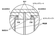
- FIG. 1 is a vertical cross-sectional view of the ceramic heater with a shaft of the present embodiment.
- the ceramic heater with a shaft includes a ceramic plate, a ceramic shaft, a conductive film, a recess (see FIG. 2), and a connecting member.
- An RF electrode and a resistance heating element are embedded in the ceramic plate.
- the RF electrode is an electrode to which a high frequency voltage is applied when generating plasma.
- the RF feeding rod is housed in the internal space of the ceramic shaft, and is joined to the RF electrode from the surface of the ceramic plate opposite to the wafer mounting surface.
- the resistance heating element heats the ceramic plate when energized.
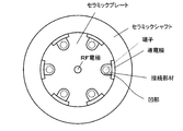
- the resistance heating elements are provided in each of the plurality (three) zones of the ceramic plate. Two terminals are provided independently for each resistance heating element.
- the ceramic shaft is a hollow shaft bonded to the surface of the ceramic plate opposite to the wafer mounting surface by direct bonding.
- the conductive film is provided along the axial direction (vertical direction) so as to run along the inner peripheral surface of the ceramic shaft.
- the conductive film may be formed by printing, plating, or the like, or may be formed by an AD method, a thermal spraying method, a CVD method, a PVD method, or the like.
- Two conductive films are provided for each resistance heating element.
- the recess is a U-shaped groove provided so as to reach the terminal of the resistance heating element from the surface of the ceramic plate opposite to the wafer mounting surface (see FIG. 3). The bottom surface of the terminal is exposed on the bottom surface of the recess.
- the surface of the conductive film is exposed on the side surface of the recess.
- the connecting member is filled in the recess and electrically connects the lower surface of the terminal of the resistance heating element and the surface of the conductive film.
- the connecting member is made by melting and then solidifying the brazing material placed in the recess.
- the connecting member is filled in the recess.
- the lower surface of the terminal is exposed on the bottom surface of the recess, and the surface of the conductive film is exposed on the side surface of the recess.
- the connecting member is in surface contact with the lower surface of the terminal of the resistance heating element and is in surface contact with the surface of the conductive film. Therefore, the reliability of the electrical connection between the resistance heating element and the conductive film is higher than in the case where the terminal of the resistance heating element and the conductive film are connected by a wire.
- the rod for supplying power to the resistance heating element is arranged in the internal space of the ceramic shaft, the number of rods is limited, and the number of resistance heating elements is also limited accordingly, but here instead of the rod Since a conductive film is used, it is possible to handle more resistance heating elements.
- the surfaces of the conductive film and the connecting member may be covered with an insulating film.
- the insulating film is preferably an aerosol deposition (AD) film or a thermal sprayed film.
- AD aerosol deposition
- the AD method (including the plasma AD method) is suitable for accurately forming a thin film of fine ceramic particles.
- the ceramic particles can be formed by the impact solidification phenomenon, it is not necessary to sinter the ceramic particles at a high temperature.
- the electrostatic electrode may be embedded in the ceramic plate.
- the present invention can be used for, for example, film forming processes such as transporting, exposing, and CVD of semiconductor wafers, and microfabrication such as cleaning, etching, and dicing.
Landscapes
- Chemical & Material Sciences (AREA)
- Engineering & Computer Science (AREA)
- Ceramic Engineering (AREA)
- Inorganic Chemistry (AREA)
- Physics & Mathematics (AREA)
- Plasma & Fusion (AREA)
- Analytical Chemistry (AREA)
- Resistance Heating (AREA)
- Container, Conveyance, Adherence, Positioning, Of Wafer (AREA)
- Chemical Vapour Deposition (AREA)
Priority Applications (4)
| Application Number | Priority Date | Filing Date | Title |
|---|---|---|---|
| CN202080050721.7A CN114175851B (zh) | 2019-07-16 | 2020-06-10 | 带轴的陶瓷加热器 |
| JP2021532729A JP7240499B2 (ja) | 2019-07-16 | 2020-06-10 | シャフト付きセラミックヒータ |
| KR1020217037422A KR102626667B1 (ko) | 2019-07-16 | 2020-06-10 | 샤프트 부착 세라믹 히터 |
| US17/451,915 US12284729B2 (en) | 2019-07-16 | 2021-10-22 | Ceramic heater with shaft |
Applications Claiming Priority (2)
| Application Number | Priority Date | Filing Date | Title |
|---|---|---|---|
| JP2019130905 | 2019-07-16 | ||
| JP2019-130905 | 2019-07-16 |
Related Child Applications (1)
| Application Number | Title | Priority Date | Filing Date |
|---|---|---|---|
| US17/451,915 Continuation US12284729B2 (en) | 2019-07-16 | 2021-10-22 | Ceramic heater with shaft |
Publications (1)
| Publication Number | Publication Date |
|---|---|
| WO2021010062A1 true WO2021010062A1 (ja) | 2021-01-21 |
Family
ID=74210581
Family Applications (1)
| Application Number | Title | Priority Date | Filing Date |
|---|---|---|---|
| PCT/JP2020/022834 Ceased WO2021010062A1 (ja) | 2019-07-16 | 2020-06-10 | シャフト付きセラミックヒータ |
Country Status (5)
| Country | Link |
|---|---|
| US (1) | US12284729B2 (https=) |
| JP (1) | JP7240499B2 (https=) |
| KR (1) | KR102626667B1 (https=) |
| CN (1) | CN114175851B (https=) |
| WO (1) | WO2021010062A1 (https=) |
Citations (4)
| Publication number | Priority date | Publication date | Assignee | Title |
|---|---|---|---|---|
| JP2006517740A (ja) * | 2003-01-17 | 2006-07-27 | ゼネラル・エレクトリック・カンパニイ | ウェーハ加工装置及びその製造方法 |
| JP2007173828A (ja) * | 2005-12-21 | 2007-07-05 | General Electric Co <Ge> | エッチング耐性ウェーハ加工装置及びその製造方法 |
| JP2016536803A (ja) * | 2013-09-16 | 2016-11-24 | アプライド マテリアルズ インコーポレイテッドApplied Materials,Incorporated | 温度プロファイル制御装置を有する加熱基板支持体 |
| JP2017162878A (ja) * | 2016-03-07 | 2017-09-14 | 日本特殊陶業株式会社 | 基板支持装置 |
Family Cites Families (10)
| Publication number | Priority date | Publication date | Assignee | Title |
|---|---|---|---|---|
| JP2001237304A (ja) * | 2000-02-21 | 2001-08-31 | Ibiden Co Ltd | 半導体製造・検査装置用セラミック基板 |
| WO2003015157A1 (en) * | 2001-08-10 | 2003-02-20 | Ibiden Co., Ltd. | Ceramic joint body |
| JP4133958B2 (ja) * | 2004-08-04 | 2008-08-13 | 日本発条株式会社 | ワークを加熱または冷却するための装置と、その製造方法 |
| JP5236927B2 (ja) | 2007-10-26 | 2013-07-17 | 信越化学工業株式会社 | 耐腐食性積層セラミックス部材 |
| JP2009182139A (ja) | 2008-01-30 | 2009-08-13 | Tokyo Electron Ltd | 載置台構造及び処理装置 |
| CN105282877B (zh) * | 2014-06-17 | 2019-10-25 | 住友电气工业株式会社 | 用于半导体制造装置的陶瓷加热器 |
| JP6560150B2 (ja) * | 2016-03-28 | 2019-08-14 | 日本碍子株式会社 | ウエハ載置装置 |
| WO2018159687A1 (ja) * | 2017-03-02 | 2018-09-07 | 日本碍子株式会社 | ウエハ加熱装置 |
| JP2019040939A (ja) * | 2017-08-23 | 2019-03-14 | 住友電気工業株式会社 | ウエハ載置台 |
| JP7109953B2 (ja) | 2018-03-26 | 2022-08-01 | 日本特殊陶業株式会社 | 加熱装置 |
-
2020
- 2020-06-10 JP JP2021532729A patent/JP7240499B2/ja active Active
- 2020-06-10 CN CN202080050721.7A patent/CN114175851B/zh active Active
- 2020-06-10 KR KR1020217037422A patent/KR102626667B1/ko active Active
- 2020-06-10 WO PCT/JP2020/022834 patent/WO2021010062A1/ja not_active Ceased
-
2021
- 2021-10-22 US US17/451,915 patent/US12284729B2/en active Active
Patent Citations (4)
| Publication number | Priority date | Publication date | Assignee | Title |
|---|---|---|---|---|
| JP2006517740A (ja) * | 2003-01-17 | 2006-07-27 | ゼネラル・エレクトリック・カンパニイ | ウェーハ加工装置及びその製造方法 |
| JP2007173828A (ja) * | 2005-12-21 | 2007-07-05 | General Electric Co <Ge> | エッチング耐性ウェーハ加工装置及びその製造方法 |
| JP2016536803A (ja) * | 2013-09-16 | 2016-11-24 | アプライド マテリアルズ インコーポレイテッドApplied Materials,Incorporated | 温度プロファイル制御装置を有する加熱基板支持体 |
| JP2017162878A (ja) * | 2016-03-07 | 2017-09-14 | 日本特殊陶業株式会社 | 基板支持装置 |
Also Published As
| Publication number | Publication date |
|---|---|
| CN114175851B (zh) | 2024-06-25 |
| KR102626667B1 (ko) | 2024-01-17 |
| US20220046762A1 (en) | 2022-02-10 |
| CN114175851A (zh) | 2022-03-11 |
| JPWO2021010062A1 (https=) | 2021-01-21 |
| US12284729B2 (en) | 2025-04-22 |
| JP7240499B2 (ja) | 2023-03-15 |
| KR20210153679A (ko) | 2021-12-17 |
Similar Documents
| Publication | Publication Date | Title |
|---|---|---|
| JP6428456B2 (ja) | 静電チャック装置 | |
| US11004715B2 (en) | Substrate supporting device | |
| JP6497248B2 (ja) | ウェハ保持体 | |
| JP5117146B2 (ja) | 加熱装置 | |
| KR19980070688A (ko) | 세라믹 부재와 전력 공급용 커넥터의 접합 구조체 | |
| JP4858319B2 (ja) | ウェハ保持体の電極接続構造 | |
| JP2018006737A (ja) | 保持装置および保持装置の製造方法 | |
| WO2021002168A1 (ja) | シャフト付きセラミックヒータ | |
| JP4321857B2 (ja) | セラミックスの接合構造 | |
| JP2003178937A (ja) | 半導体製造装置およびそれに使用される給電用電極部材 | |
| JP7050455B2 (ja) | 静電チャックの製造方法 | |
| JP5562086B2 (ja) | 加熱用部材およびこれを用いた加熱装置 | |
| JP7143256B2 (ja) | ウエハ載置台及びその製法 | |
| KR101387916B1 (ko) | 히터 겸용 정전척 | |
| JP6699765B2 (ja) | ウェハ保持体 | |
| WO2021010062A1 (ja) | シャフト付きセラミックヒータ | |
| JP7174159B2 (ja) | シャフト付きセラミックヒータ | |
| JP7303302B2 (ja) | シャフト付きセラミックヒータ | |
| JP2018006393A (ja) | 保持装置 | |
| KR100979915B1 (ko) | 정전척 및 히터 | |
| JP5674192B2 (ja) | 静電チャックおよびその製造方法。 | |
| WO2000026995A1 (fr) | Structure de connexion de borne d'entree electrique | |
| JP2024139299A (ja) | 保持装置 | |
| CN121605794A (zh) | 陶瓷基座 | |
| KR20100079480A (ko) | 히터 및 반도체 소자의 제조장치 |
Legal Events
| Date | Code | Title | Description |
|---|---|---|---|
| 121 | Ep: the epo has been informed by wipo that ep was designated in this application |
Ref document number: 20839560 Country of ref document: EP Kind code of ref document: A1 |
|
| ENP | Entry into the national phase |
Ref document number: 2021532729 Country of ref document: JP Kind code of ref document: A |
|
| ENP | Entry into the national phase |
Ref document number: 20217037422 Country of ref document: KR Kind code of ref document: A |
|
| NENP | Non-entry into the national phase |
Ref country code: DE |
|
| 122 | Ep: pct application non-entry in european phase |
Ref document number: 20839560 Country of ref document: EP Kind code of ref document: A1 |