WO2020170757A1 - サーミスタの製造方法 - Google Patents
サーミスタの製造方法 Download PDFInfo
- Publication number
- WO2020170757A1 WO2020170757A1 PCT/JP2020/003618 JP2020003618W WO2020170757A1 WO 2020170757 A1 WO2020170757 A1 WO 2020170757A1 JP 2020003618 W JP2020003618 W JP 2020003618W WO 2020170757 A1 WO2020170757 A1 WO 2020170757A1
- Authority
- WO
- WIPO (PCT)
- Prior art keywords
- electrode layer
- thermistor
- protective film
- base electrode
- chip
- Prior art date
- Legal status (The legal status is an assumption and is not a legal conclusion. Google has not performed a legal analysis and makes no representation as to the accuracy of the status listed.)
- Ceased
Links
Images



Classifications
-
- H—ELECTRICITY
- H01—ELECTRIC ELEMENTS
- H01C—RESISTORS
- H01C1/00—Details
- H01C1/02—Housing; Enclosing; Embedding; Filling the housing or enclosure
- H01C1/028—Housing; Enclosing; Embedding; Filling the housing or enclosure the resistive element being embedded in insulation with outer enclosing sheath
-
- H—ELECTRICITY
- H01—ELECTRIC ELEMENTS
- H01C—RESISTORS
- H01C1/00—Details
- H01C1/14—Terminals or tapping points specially adapted for resistors; Arrangements of terminals or tapping points on resistors
- H01C1/142—Terminals or tapping points specially adapted for resistors; Arrangements of terminals or tapping points on resistors the terminals or tapping points being coated on the resistive element
-
- H—ELECTRICITY
- H01—ELECTRIC ELEMENTS
- H01C—RESISTORS
- H01C1/00—Details
- H01C1/14—Terminals or tapping points specially adapted for resistors; Arrangements of terminals or tapping points on resistors
- H01C1/148—Terminals or tapping points specially adapted for resistors; Arrangements of terminals or tapping points on resistors the terminals embracing or surrounding the resistive element
-
- H—ELECTRICITY
- H01—ELECTRIC ELEMENTS
- H01C—RESISTORS
- H01C17/00—Apparatus or processes specially adapted for manufacturing resistors
- H01C17/02—Apparatus or processes specially adapted for manufacturing resistors adapted for manufacturing resistors with envelope or housing
-
- H—ELECTRICITY
- H01—ELECTRIC ELEMENTS
- H01C—RESISTORS
- H01C17/00—Apparatus or processes specially adapted for manufacturing resistors
- H01C17/06—Apparatus or processes specially adapted for manufacturing resistors adapted for coating resistive material on a base
- H01C17/065—Apparatus or processes specially adapted for manufacturing resistors adapted for coating resistive material on a base by thick film techniques, e.g. serigraphy
- H01C17/06506—Precursor compositions therefor, e.g. pastes, inks, glass frits or green body
- H01C17/06513—Precursor compositions therefor, e.g. pastes, inks, glass frits or green body characterised by the resistive component
- H01C17/06553—Precursor compositions therefor, e.g. pastes, inks, glass frits or green body characterised by the resistive component composed of a combination of metals and oxides
-
- H—ELECTRICITY
- H01—ELECTRIC ELEMENTS
- H01C—RESISTORS
- H01C17/00—Apparatus or processes specially adapted for manufacturing resistors
- H01C17/28—Apparatus or processes specially adapted for manufacturing resistors adapted for applying terminals
- H01C17/281—Apparatus or processes specially adapted for manufacturing resistors adapted for applying terminals by thick film techniques
- H01C17/283—Precursor compositions therefor, e.g. pastes, inks, glass frits
-
- H—ELECTRICITY
- H01—ELECTRIC ELEMENTS
- H01C—RESISTORS
- H01C7/00—Non-adjustable resistors formed as one or more layers or coatings; Non-adjustable resistors made from powdered conducting material or powdered semi-conducting material with or without insulating material
- H01C7/008—Thermistors
-
- H—ELECTRICITY
- H01—ELECTRIC ELEMENTS
- H01C—RESISTORS
- H01C17/00—Apparatus or processes specially adapted for manufacturing resistors
- H01C17/006—Apparatus or processes specially adapted for manufacturing resistors adapted for manufacturing resistor chips
-
- H—ELECTRICITY
- H01—ELECTRIC ELEMENTS
- H01C—RESISTORS
- H01C17/00—Apparatus or processes specially adapted for manufacturing resistors
- H01C17/28—Apparatus or processes specially adapted for manufacturing resistors adapted for applying terminals
- H01C17/281—Apparatus or processes specially adapted for manufacturing resistors adapted for applying terminals by thick film techniques
Definitions
- the present invention is directed to manufacturing a thermistor including a thermistor chip made of a thermistor material, a protective film formed on the surface of the thermistor chip, and electrode portions formed at both ends of the thermistor chip. It is about the method.
- the present application claims priority based on Japanese Patent Application No. 2019-030527 filed in Japan on Feb. 22, 2019, the contents of which are incorporated herein by reference.
- the above-mentioned thermistor (thermistor material) has a characteristic that the electric resistance changes according to temperature, and is applied to temperature compensation of various electronic devices, temperature sensors, and the like.
- a chip type thermistor mounted on a circuit board has been widely used.
- the thermistor described above has a structure in which a thermistor chip and a pair of electrode portions are formed at both ends of the thermistor chip.
- the thermistor chip has a property that it is weak against acids and alkalis and is easily reduced. If the composition changes due to these reactions, the characteristics may change. Therefore, for example, as shown in Patent Document 1, a technique of forming a protective film on the surface of the thermistor chip has been proposed. Note that the protective film is required to have resistance to a plating solution, environment resistance, insulation, etc. in order to suppress deterioration of the thermistor chip in subsequent steps or during use.
- a glass paste is applied to the surface of the thermistor chip and baked to form a protective film made of glass. Further, since the electrode portions are formed at both ends of the thermistor chip, the protective film is not formed on the end surface of the thermistor where the electrode portions are formed.
- the electrode portion is formed by applying a conductive paste containing a conductive material such as Ag to both ends of the thermistor chip and firing the applied paste. Further, a Ni plating layer or a Sn plating layer is formed on the surface of the electrode portion made of the fired body.
- a protective film is formed on both sides of a thermistor wafer made of a thermistor material, and after cutting this into strips, a protective film is further formed on the cut surface, which is After cutting into chips, electrode portions were formed on both end faces of the thermistor chip (cut faces at the time of chip formation), and a plating layer was formed on the surfaces of the electrode portions.
- the strip-shaped thermistor material is easily broken during handling, and it is difficult to efficiently manufacture the thermistor.
- miniaturization of the thermistor has been demanded, the cross-sectional area of the strip becomes small, and it tends to be broken.
- the conductive paste is applied and fired after forming into chips to form the electrode portion made of a fired body, the electrode portion may be emptied due to uneven application of the conductive paste or contamination of foreign matter into the conductive paste. Porosity sometimes resulted in a porous structure.
- the plating solution may enter the inside of the electrode portion and the thermistor chip and the plating solution may come into contact with each other to deteriorate the thermistor chip. Further, the plating metal may be deposited on the interface between the thermistor chip and the electrode portion, and the resistance value may significantly change before and after plating.
- the present invention has been made in view of the above-mentioned circumstances, suppresses the occurrence of breakage and the like during manufacturing, and can stably manufacture a thermistor, and forms a plating layer on the surface of the electrode part. Even in such a case, it is an object of the present invention to provide a method for manufacturing a thermistor capable of suppressing the invasion of a plating solution into the electrode portion and manufacturing a thermistor having stable characteristics.
- a method for manufacturing a thermistor of the present invention is a thermistor chip having a columnar shape, a protective film formed on the surface of the thermistor chip, and electrode portions formed on both ends of the thermistor chip.
- a method of manufacturing a thermistor for manufacturing a thermistor comprising: a base electrode layer forming step of forming a base electrode layer by applying a conductive paste to both surfaces of a thermistor wafer made of a thermistor material and baking the paste; A chipping step of cutting the thermistor wafer with the electrode layer formed into chips to obtain a thermistor chip with a base electrode layer, and a protective film for forming a protective film made of an oxide on the entire surface of the thermistor chip with the base electrode layer Forming step, a cover electrode layer forming step of forming a cover electrode layer by applying a conductive paste on the surface of the protective film formed on the end surface of the thermistor chip with the underlying electrode layer and baking the paste, and the underlying electrode layer And a conduction heat treatment step of performing heat treatment so that the cover electrode layer and the cover electrode layer are electrically connected to each other, and the electrode portion having the base electrode layer and the cover electrode layer is formed.
- the base electrode layer is cut and made into chips. It is possible to suppress the occurrence of breakage etc. without handling it in a state. Therefore, the handleability at the time of manufacturing is improved, and the thermistor can be manufactured efficiently and with high yield. Further, in the method of manufacturing a thermistor of the present invention, in the protective film forming step, since the protective film made of oxide is formed on the entire surface of the thermistor chip with the underlying electrode layer, the thermistor chip is reliably protected by the protective film. can do.
- the method of manufacturing a thermistor of the present invention includes the cover electrode layer forming step and the conduction heat treatment step, the electrode portion has a two-layer structure of the base electrode layer and the cover electrode layer, and The pores and the pores of the cover electrode layer do not communicate with each other, and the penetration of the plating solution is blocked at the interface between the cover electrode layer and the base electrode layer in the subsequent plating step. It is possible to suppress the contact with. Further, it is possible to suppress the plating metal from being deposited on the interface between the thermistor chip and the electrode portion.
- a conduction heat treatment step of performing heat treatment so that the base electrode layer and the cover electrode layer are electrically conducted is provided, even if a protective film is formed between the base electrode layer and the cover electrode layer.
- the base electrode layer and the cover electrode layer can be electrically connected to each other, and the function as the electrode portion can be secured.
- the protective film is made of silicon oxide.
- the protective film since the protective film is made of silicon oxide, it has excellent environmental resistance, and the cover electrode layer can be reliably formed on the surface of this protective film, and the cover electrode layer and the base electrode layer can be reliably formed.
- the two-layer structure electrode part can be stably formed.
- the protective film forming step is performed by immersing the thermistor chip with the underlying electrode layer in a reaction solution containing silicon alkoxide, water, an organic solvent and an alkali to dissolve the silicon alkoxide. It is preferable to form the protective film by depositing silicon oxide on the surface of the thermistor chip with the underlying electrode layer by decomposition and polycondensation reaction. In this case, silicon oxide is deposited by polymerization of the hydrolyzate of silicon alkoxide starting from terminal oxygen or hydroxyl group on the surface of the thermistor chip, so that the adhesion between the thermistor chip and the protective film is excellent.
- the silicon oxide is deposited from the surface of the thermistor chip, the coverage of the corners and the irregularities is excellent. Therefore, it is possible to manufacture a thermistor which can be stably used without deterioration of the characteristics of the thermistor chip.
- a conductive oxide layer is formed on the surface of the thermistor wafer, and thereafter, a conductive paste containing metal powder is applied and baked. It may be configured. In this case, by forming a conductive oxide layer on the surface of the thermistor wafer, it is possible to improve the bonding reliability between the thermistor chip and the base electrode layer.
- the base electrode layer is formed by applying and firing a glass-containing metal paste containing metal powder and glass powder. May be In this case, since the base electrode layer is formed by firing the metal paste containing glass, the adhesion of the base electrode layer can be improved.
- the cover electrode layer forming step forms the cover electrode layer by applying and baking a glass-containing metal paste containing metal powder and glass powder. May be In this case, since the cover electrode layer is formed by firing the glass-containing metal paste, the glass and the protective film react with each other in the conductive heat treatment step, so that at least a part of the protective film can be efficiently eliminated. Therefore, the base electrode layer and the cover electrode layer can be sufficiently conducted.
- the protective film forming step is performed.
- the configuration may be implemented.
- the chip forming step since it has a chamfering step of chamfering the thermistor chip with the underlying electrode layer, it is possible to suppress the occurrence of cracks and chips at the corners of the thermistor chip, and more efficiently, In addition, it becomes possible to manufacture the thermistor with higher yield.
- the present invention it is possible to suppress the occurrence of breakage and the like at the time of manufacturing, to stably manufacture the thermistor, and even when a plating layer is formed on the surface of the electrode part, It is possible to provide a method for manufacturing a thermistor which can suppress the invasion of a plating solution and can manufacture a thermistor having stable characteristics.
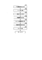
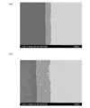
- FIG. 2 is an enlarged explanatory view of the vicinity of an electrode portion of the thermistor shown in FIG. 1. It is a flowchart which shows the manufacturing method of the thermistor which concerns on this embodiment. It is an observation photograph of the electrode part vicinity of the thermistor manufactured in the Example. 3 is an observation photograph of an interface between a thermistor chip and a protective film of a thermistor manufactured in an example.
- the thermistor 10 has, for example, a prism shape, and has a thermistor chip 11, a protective film 15 formed on the surface of the thermistor chip 11, and both ends of the thermistor chip 11. And an electrode portion 20 formed on each of the portions.
- the electrode portion 20 is configured to directly contact the thermistor chip 11.
- the thermistor chip 11 has a characteristic that the electric resistance changes according to the temperature.
- the thermistor chip 11 has low resistance to acids and alkalis, and its composition may change due to reduction reaction or the like, resulting in a large change in characteristics. Therefore, in this embodiment, the protective film 15 is formed to protect the thermistor chip 11.
- the protective film 15 is required to have resistance to a plating solution, environment resistance, and insulation. Therefore, in the present embodiment, the protective film 15 may be made of silicon oxide, specifically, SiO 2 . In addition, in the present embodiment, the thickness of the protective film 15 may be 50 nm or more. The lower limit of the thickness of the protective film 15 is preferably 50 nm or more, more preferably 100 nm or more, because the protective film may be discontinuous. On the other hand, the upper limit of the thickness of the protective film 15 is preferably 3 ⁇ m or less, which is the limit of the erosion effect of the glass frit included in the electrode portion 20 on the protective film 15, and stabilizes the above-mentioned erosion effect to reduce the electric resistance. From the viewpoint of suppressing variations, the thickness is more preferably 2 ⁇ m or less.
- the electrode section 20 has a two-layer structure including a base electrode layer 21 formed on the end surface of the thermistor chip 11 and a cover electrode layer 22 laminated on the base electrode layer 21.
- the base electrode layer 21 is formed by firing a conductive paste as described later, and may be made of a fired body of Ag in the present embodiment. In this case, holes are present inside the base electrode layer 21.
- the cover electrode layer 22 is also formed by firing a conductive paste as described later, and may be made of a fired body of Ag in the present embodiment. In this case, holes also exist inside the cover electrode layer 22.
- the thickness t1 of the base electrode layer 21 is set within the range of 2 ⁇ m or more and 20 ⁇ m or less. If it is less than 2 ⁇ m, the amount of glass is insufficient and the erosion of the protective film 15 is likely to be insufficient. If the amount of glass in the paste is increased to secure the erosion of the protective film 15, the percolation of the conductive particles becomes insufficient and the resistance value increases. There is a risk of doing it. On the other hand, when it exceeds 20 ⁇ m, the erosion effect of the protective film 15 by the glass is saturated, resulting in material loss.
- the lower limit of the thickness t1 of the base electrode layer 21 is preferably 3 ⁇ m or more, more preferably 5 ⁇ m or more.
- the upper limit of the thickness t1 of the base electrode layer 21 is preferably 15 ⁇ m or less, and more preferably 10 ⁇ m or less.
- the thickness t2 of the cover electrode layer 22 is set within the range of 3 ⁇ m or more and 20 ⁇ m or less. If it is less than 3 ⁇ m, the amount of glass is insufficient and the erosion of the protective film 15 tends to be insufficient. If the amount of glass in the paste is increased to ensure the erosion of the protective film 15, the percolation of the conductive particles becomes insufficient and the resistance value increases. On the other hand, when the thickness exceeds 20 ⁇ m, the erosion effect of the protective film 15 by the glass is saturated, resulting in material loss, and the shape of the thermistor 10 swells only in the electrode portion, resulting in poor shape. ..
- the lower limit of the thickness t2 of the cover electrode layer 22 is preferably 4 ⁇ m or more, more preferably 5 ⁇ m or more.
- the upper limit of the thickness t2 of the cover electrode layer 22 is preferably 15 ⁇ m or less, more preferably 10 ⁇ m or less.
- a Ni plating layer 31 is formed on the surface of the electrode portion 20, and a Sn plating layer 32 is formed so as to be stacked on the Ni plating layer 31.
- Ni of the Ni plating layer 31 may penetrate into the electrode portion 20. The Ni penetrates into the interface between the base electrode layer 21 and the cover electrode layer 22, but does not reach the joint interface between the thermistor chip 11 and the electrode portion 20 (base electrode layer 21).
- the base electrode layers 21 are formed on both surfaces of the thermistor wafer made of the thermistor material.
- a conductive oxide layer made of a conductive oxide (ruthenium oxide in the present embodiment) is formed on both surfaces of the thermistor wafer.
- the base electrode layer 21 is formed by applying a conductive paste containing Ag powder and glass powder on the conductive oxide layer and baking the conductive paste.
- the surface layer of the base electrode layer 21 is composed of a fired body of Ag.
- Chiping step S02 the thermistor wafer on which the base electrode layer 21 is formed is cut into chips to obtain a thermistor chip 11 on which the base electrode layer 21 is formed (hereinafter referred to as a thermistor chip with a base electrode layer). That is, the thickness direction of the thermistor wafer becomes the thickness direction of the thermistor chip 11, and the base electrode layers 21 are formed on both end faces of the thermistor chip 11 in the thickness direction.
- the protective film 15 is formed on the surface of the thermistor chip with the underlying electrode layer.
- the thermistor chip with the underlying electrode layer is protected by immersing the thermistor chip 11 in a reaction solution containing silicon alkoxide, water, an organic solvent and an alkali to deposit silicon oxide (SiO 2 ) on the surface of the thermistor chip 11.
- the film 15 may be formed.
- the protective film 15 is also formed on the surface of the base electrode layer 21.
- the thickness of the protective film 15 formed is preferably 50 nm or more. The thickness is more preferably 100 ⁇ m or more.
- silicon alkoxide for example, ethyl orthosilicate or an oligomer of ethyl orthosilicate (silicate 40 manufactured by Tama Chemical Co., Ltd.), or methyl orthosilicate or an oligomer of methyl orthosilicate (MS51 manufactured by Tama Chemical Co., Ltd.) can be used.
- organic solvent water-soluble alcohols such as methanol, ethanol and isopropanol, organic solvents such as ketones compatible with these, and mixtures thereof can be used.
- alkali inorganic alkalis such as sodium hydroxide, potassium hydroxide and ammonia, amines such as ethanolamine and ethylenediamine, and the like can be used.
- the cover electrode layer 22 is formed on the protective film 15 formed on the surface of the base electrode layer 21.
- the cover electrode layer 22 is formed by applying a conductive paste containing Ag powder and glass powder to the surface of the protective film 15 and baking the conductive paste.
- the cover electrode layer 22 is a baked body of Ag. Will be composed of.
- Conduction heat treatment step S06 Next, heat treatment is performed so that the base electrode layer 21 and the cover electrode layer 22 are electrically connected.
- the conduction heat treatment step S06 at least a part of the protective film 15 interposed between the base electrode layer 21 and the cover electrode layer 22 disappears so that the base electrode layer 21 and the cover electrode layer 22 are electrically connected. become.
- the heating temperature is equal to or higher than the melting points of both the glass frit in the base electrode layer 21 and the glass frit in the cover electrode layer 22. That is, although the optimum temperature changes depending on the glass frit used, it is preferably higher than the melting point of the glass frit in the cover electrode layer 22 by 50° C.
- the heating temperature is preferably 900° C. or lower from the viewpoint of the glass floating on the surface of the cover electrode layer 22.
- the melting point of the glass frit in the cover electrode layer 22 is preferably higher than the melting point of the glass frit in the base electrode layer 21.
- the holding time at the heating temperature is preferably within the range of 5 minutes or more and 60 minutes or less. Further, it is preferable that the atmosphere is an air atmosphere.
- the base electrode layer forming step S01 By the base electrode layer forming step S01, the protective film forming step S04, the cover electrode layer forming step S05, and the conduction heat treatment step S06, the two-layer structure electrode portion 20 including the base electrode layer 21 and the cover electrode layer 22 is formed. Will be.
- a metal plating layer is formed on the surface of the electrode portion 20.
- the Ni plating layer 31 is formed on the surface of the electrode portion 20, and then the Sn plating layer 32 is formed so as to be stacked on the Ni plating layer 31.
- the Ni plating layer 31 and the Sn plating layer 32 described above are formed by wet barrel plating.
- the plating solution penetrates into the electrode portion 20.
- the holes inside the base electrode layer 21 and the holes inside the cover electrode layer 22 do not communicate with each other, the penetration of the plating solution at the bonding interface between the base electrode layer 21 and the cover electrode layer 22 is prevented. Will be suppressed.
- the thermistor 10 according to the present embodiment is manufactured by the above process.
- the base electrode layer 21 is formed on the surface of the thermistor wafer made of the thermistor material, and then the base electrode layer 21 is cut into chips. Since the thermistor material in a strip shape is not handled, breakage and the like can be suppressed. Therefore, the handleability during manufacturing is improved, and the thermistor 10 can be manufactured efficiently and with high yield. Further, in the present embodiment, in the protective film forming step S04, the protective film 15 made of oxide is formed on the entire surface of the thermistor chip 11 on which the base electrode layer 21 is formed. Can be reliably protected.
- the electrode portion 20 has a two-layer structure of the base electrode layer 21 and the cover electrode layer 22, and the base electrode layer In the plating step S07, the invasion of the plating solution is blocked at the interface between the cover electrode layer 22 and the base electrode layer 21 without the holes in 21 and the holes in the cover electrode layer 22 communicating with each other.
- the contact between the thermistor chip 11 and the plating solution can be suppressed. Further, it is possible to prevent the plating metal from depositing on the interface between the thermistor chip 11 and the electrode portion 20.
- the conduction heat treatment step S06 is performed to perform heat treatment so that the base electrode layer 21 and the cover electrode layer 22 are electrically conducted, the base electrode layer 21 and the cover electrode layer 22 are separated from each other. Even if the protective film 15 is formed in between, the base electrode layer 21 and the cover electrode layer 22 can be electrically connected to each other, and the function as the electrode portion 20 can be ensured.
- the protective film 15 is made of silicon oxide, it has excellent environmental resistance, and the cover electrode layer 22 can be reliably formed on the surface of the protective film 15.
- the electrode portion 20 having a two-layer structure of the base electrode layer 21 and the cover electrode layer 22 can be stably formed.
- the thermistor chip 11 on which the base electrode layer 21 is formed is immersed in a reaction solution containing silicon alkoxide, water, an organic solvent and an alkali to hydrolyze the silicon alkoxide.
- the protective film 15 is formed by depositing silicon oxide on the surface of the thermistor chip 11 by the polycondensation reaction, the hydrolyzate of the silicon alkoxide starts from the terminal oxygen or hydroxyl group on the surface of the thermistor chip 11. Since the silicon oxide is deposited by the polymerization, the adhesion between the thermistor chip 11 and the protective film 15 is excellent.
- the silicon oxide is deposited from the surface of the thermistor chip 11, the corners and the irregularities are excellent in coverage. Therefore, it is possible to manufacture the thermistor 10 that can be used stably without deterioration of the characteristics of the thermistor chip 11.
- a conductive oxide layer made of a conductive oxide is formed on the surface of the thermistor wafer, and the conductive oxide layer is formed on the conductive oxide layer. Since the base electrode layer 21 is formed by applying and firing the conductive paste, it is possible to improve the bonding reliability between the thermistor chip 11 and the base electrode layer 21. Further, since the conductive paste containing Ag powder and glass powder is used as the conductive paste, the adhesion of the base electrode layer 21 can be improved, and the surface layer of the base electrode layer 21 is made of a fired body of Ag. Can be configured.
- the conduction heat treatment step S06 in the cover electrode layer forming step S05, since the cover electrode layer 22 is formed by applying and firing a conductive paste containing Ag powder and glass powder, the conduction heat treatment step S06. In the above, by reacting the glass with the protective film 15, at least a part of the protective film 15 can be efficiently eliminated, and the base electrode layer 21 and the cover electrode layer 22 can be sufficiently conducted. ..
- the chamfering processing step S03 for chamfering the thermistor chip 11 on which the base electrode layer 21 is formed is included, so that cracks at the corners of the thermistor chip 11 may occur.
- the occurrence of chipping can be suppressed, and the thermistor 10 can be manufactured with higher efficiency and higher yield.
- the present invention is not limited to this, and can be appropriately modified without departing from the technical idea of the invention.
- the thermistor chip is immersed in the reaction solution to form the protective film in the present embodiment
- the present invention is not limited to this, and the protective film may be formed by other means. ..
- a glass paste may be applied and baked to form a protective film.
- An ethanol dispersion of RuO 2 powder was spin-coated on both sides of a thermistor wafer having a size of 38 ⁇ 55 mm and a thickness of 0.36 mm and baked at 250° C., and then a conductive oxide layer was formed.
- the thermistor wafer on which the base electrode layer was formed was cut into chips by dicing into 0.18 mm square. After chipping, chamfering was performed by barreling.
- the thermistor chip was put in a water-ethanol mixed solvent, and while stirring, 5.2 g of ethyl orthosilicate and 16.6 g of an aqueous NaOH solution (0.2 mol/L) were added to the whole surface of the thermistor chip to oxidize silicon.
- a protective film made of a material was formed.
- baking was performed at 700° C. after the film formation, and the film formation and baking were repeatedly performed, and the thickness of the protective film was set to 1 ⁇ m.
- the cover electrode layer was formed by baking under the conditions of the atmosphere, the heating temperature: 750° C., and the holding time at the heating temperature: 10 minutes.
- the baking process also serves as a conduction heat treatment.
- the Ni plating layer and the Sn plating layer were formed by wet barrel plating.
- FIG. 4 The observation result of the electrode portion of the thermistor obtained through the above steps is shown in FIG. 4, and the observation result of the interface between the thermistor chip and the protective film is shown in FIG.
- the SEM image of FIG. 4A a part of the protective film formed between the base electrode layer and the cover electrode layer has disappeared, and the base electrode layer and the cover electrode layer are electrically connected. Is confirmed.
- the Ni mapping diagram of FIG. 4B it is confirmed that the penetration of Ni is stopped and the thermistor chip and the plating solution are not in contact with each other.
- the magnification is 20,000 times in (a) and 50,000 times in (b).
- the protective film is formed in close contact with the region other than the electrode portion of the thermistor chip.
- the present invention it is possible to suppress the occurrence of breakage and the like during manufacturing, it is possible to stably manufacture the thermistor, and even when the plating layer is formed on the surface of the electrode portion, It was confirmed that it is possible to provide a thermistor manufacturing method capable of suppressing the penetration of the plating solution into the electrode portion and manufacturing a thermistor having stable characteristics.
Landscapes
- Engineering & Computer Science (AREA)
- Microelectronics & Electronic Packaging (AREA)
- Manufacturing & Machinery (AREA)
- Physics & Mathematics (AREA)
- Electromagnetism (AREA)
- Thermistors And Varistors (AREA)
- Apparatuses And Processes For Manufacturing Resistors (AREA)
- Details Of Resistors (AREA)
Abstract
サーミスタ材料からなるサーミスタウェハの両面に下地電極層を形成する下地電極層形成工程(S01)と、前記サーミスタウェハを切断してチップ化し、下地電極層付きサーミスタチップを得るチップ化工程(S02)と、前記下地電極層付きサーミスタチップの全面に、酸化物からなる保護膜を形成する保護膜形成工程(S03)と、前記下地電極層付きサーミスタチップの端面に導電性ペーストを塗布して焼成し、カバー電極層を形成するカバー電極層形成工程(S04)と、前記下地電極層と前記カバー電極層とが電気的に導通するように熱処理を行う導通熱処理工程(S05)と、を有し、前記下地電極と前記カバー電極とを有する前記電極部を形成する。
Description
この発明は、サーミスタ材料からなるサーミスタチップと、前記サーミスタチップの表面に形成された保護膜と、前記サーミスタチップの両端部にそれぞれ形成された電極部と、を備えたサーミスタを製造するサーミスタの製造方法に関するものである。
本願は、2019年2月22日に日本に出願された、特願2019-030527号に基づき優先権主張し、その内容をここに援用する。
本願は、2019年2月22日に日本に出願された、特願2019-030527号に基づき優先権主張し、その内容をここに援用する。
上述のサーミスタ(サーミスタ材料)においては、温度に応じて電気抵抗が変化する特性を有しており、各種電子機器の温度補償や温度センサ等に適用されている。特に、最近では、回路基板に実装されるチップ型サーミスタが広く使用されている。
上述のサーミスタは、サーミスタチップと、このサーミスタチップの両端に一対の電極部を形成した構造としている。
上述のサーミスタは、サーミスタチップと、このサーミスタチップの両端に一対の電極部を形成した構造としている。
サーミスタチップは、酸やアルカリに弱く、かつ、還元しやすい性質を有しており、これらの反応によって組成が変化すると、特性が変動してしまうおそれがあった。このため、例えば特許文献1に示すように、サーミスタチップの表面に保護膜を成膜する技術が提案されている。なお、保護膜には、その後の工程や使用時におけるサーミスタチップの劣化を抑制するために、めっき液への耐性、耐環境性、絶縁性、等が要求される。
この特許文献1においては、サーミスタチップの表面にガラスペーストを塗布して焼成することにより、ガラスからなる保護膜を成膜している。
また、サーミスタチップの両端には電極部を形成することになるため、電極部が形成されるサーミスタの端面には保護膜が形成されてない。
ここで、電極部は、サーミスタチップの両端に、例えばAg等の導電性材料を含む導電性ペーストを塗布して焼成することによって形成される。また、焼成体からなる電極部の表面には、Niめっき層やSnめっき層が形成される。
また、サーミスタチップの両端には電極部を形成することになるため、電極部が形成されるサーミスタの端面には保護膜が形成されてない。
ここで、電極部は、サーミスタチップの両端に、例えばAg等の導電性材料を含む導電性ペーストを塗布して焼成することによって形成される。また、焼成体からなる電極部の表面には、Niめっき層やSnめっき層が形成される。
従来、上述のサーミスタを製造する場合には、通常、サーミスタ材料からなるサーミスタウェハの両面に保護膜を形成し、これを短冊状に切断した後、切断面に保護膜をさらに形成し、これを切断してチップ化した後、サーミスタチップの両端面(チップ化の際の切断面)に電極部を形成し、この電極部の表面にめっき層を形成していた。
ところで、従来のように、サーミスタウェハを短冊状に切断した場合、短冊状のサーミスタ材料は取り扱い時に折損しやすく、効率良くサーミスタを製造することは困難であった。特に、最近では、サーミスタの小型化が求められており、短冊の断面積が小さくなり、さらに折損しやすい傾向にある。
また、チップ化した後に、導電性ペーストを塗布して焼成し、焼成体からなる電極部を形成する際に、導電性ペーストの塗布ムラや導電性ペーストへの異物の混入により、電極部に空孔が生じてポーラスな構造となることがあった。このような電極部に対してめっき層を形成した場合には、電極部の内部にめっき液が侵入し、サーミスタチップとめっき液とが接触して、サーミスタチップが劣化するおそれがあった。また、サーミスタチップと電極部の界面にめっき金属が析出し、めっきの前後で抵抗値が大きく変化してしまうおそれがあった。
また、チップ化した後に、導電性ペーストを塗布して焼成し、焼成体からなる電極部を形成する際に、導電性ペーストの塗布ムラや導電性ペーストへの異物の混入により、電極部に空孔が生じてポーラスな構造となることがあった。このような電極部に対してめっき層を形成した場合には、電極部の内部にめっき液が侵入し、サーミスタチップとめっき液とが接触して、サーミスタチップが劣化するおそれがあった。また、サーミスタチップと電極部の界面にめっき金属が析出し、めっきの前後で抵抗値が大きく変化してしまうおそれがあった。
この発明は、前述した事情に鑑みてなされたものであって、製造時における折損等の発生を抑制し、安定してサーミスタを製造することができるとともに、電極部の表面にめっき層を形成した場合であっても、電極部内部へのめっき液の侵入を抑制でき、特性が安定したサーミスタを製造することが可能なサーミスタの製造方法を提供することを目的とする。
上記課題を解決するために、本発明のサーミスタの製造方法は、柱状をなすサーミスタチップと、前記サーミスタチップの表面に形成された保護膜と、前記サーミスタチップの両端部にそれぞれ形成された電極部と、を備えたサーミスタを製造するサーミスタの製造方法であって、サーミスタ材料からなるサーミスタウェハの両面に導電性ペーストを塗布して焼成し、下地電極層を形成する下地電極層形成工程と、下地電極層を形成した前記サーミスタウェハを切断してチップ化し、下地電極層付きサーミスタチップを得るチップ化工程と、前記下地電極層付きサーミスタチップの全面に、酸化物からなる保護膜を形成する保護膜形成工程と、前記下地電極層付きサーミスタチップの端面に形成された前記保護膜の表面に導電性ペーストを塗布して焼成し、カバー電極層を形成するカバー電極層形成工程と、前記下地電極層と前記カバー電極層とが電気的に導通するように熱処理を行う導通熱処理工程と、を有し、前記下地電極層と前記カバー電極層とを有する前記電極部を形成することを特徴としている。
本発明のサーミスタの製造方法によれば、上述のように、サーミスタ材料からなるサーミスタウェハの表面に下地電極層を形成した後、これを切断してチップ化しているので、サーミスタ材料を短冊状の状態で取り扱うことがなく、折損等の発生を抑制できる。よって、製造時の取り扱い性が向上し、サーミスタを効率良く、かつ、歩留まり良く製造することが可能となる。
また、本発明のサーミスタの製造方法では、保護膜形成工程において、前記下地電極層付きサーミスタチップの全面に、酸化物からなる保護膜を形成しているので、保護膜によってサーミスタチップを確実に保護することができる。
また、本発明のサーミスタの製造方法では、保護膜形成工程において、前記下地電極層付きサーミスタチップの全面に、酸化物からなる保護膜を形成しているので、保護膜によってサーミスタチップを確実に保護することができる。
さらに、本発明のサーミスタの製造方法では、カバー電極層形成工程と、導通熱処理工程と、を備えているので、電極部が下地電極層とカバー電極層の2層構造となり、下地電極層内の空孔とカバー電極層の空孔とが連通することなく、その後のめっき工程において、めっき液の侵入がカバー電極層と下地電極層との界面において阻止されることになり、サーミスタチップとめっき液との接触を抑制することが可能となる。また、サーミスタチップと電極部の界面にめっき金属が析出することを抑制できる。
また、前記下地電極層と前記カバー電極層とが電気的に導通するように熱処理を行う導通熱処理工程を備えているので、下地電極層とカバー電極層との間に保護膜を形成しても、下地電極層とカバー電極層とを電気的に導通させることができ、電極部としての機能を確保することが可能となる。
また、前記下地電極層と前記カバー電極層とが電気的に導通するように熱処理を行う導通熱処理工程を備えているので、下地電極層とカバー電極層との間に保護膜を形成しても、下地電極層とカバー電極層とを電気的に導通させることができ、電極部としての機能を確保することが可能となる。
ここで、本発明のサーミスタの製造方法においては、前記保護膜は、シリコン酸化物で構成されていることが好ましい。
この場合、保護膜がシリコン酸化物で構成されているので、耐環境性に優れており、この保護膜の表面に確実にカバー電極層を形成することができ、下地電極層とカバー電極層の2層構造電極部を安定して形成することができる。
この場合、保護膜がシリコン酸化物で構成されているので、耐環境性に優れており、この保護膜の表面に確実にカバー電極層を形成することができ、下地電極層とカバー電極層の2層構造電極部を安定して形成することができる。
また、本発明のサーミスタの製造方法においては、前記保護膜形成工程は、シリコンアルコキシドと水と有機溶媒とアルカリを含む反応液に、前記下地電極層付きサーミスタチップを浸漬し、前記シリコンアルコキシドの加水分解及び重縮合反応によって前記下地電極層付きサーミスタチップの表面にシリコン酸化物を析出させることにより、前記保護膜を成膜することが好ましい。
この場合、サーミスタチップ表面の終端酸素や水酸基を起点としてシリコンアルコキシドの加水分解体が重合することで、シリコン酸化物が析出するため、サーミスタチップと保護膜との密着性に優れている。また、サーミスタチップの表面からシリコン酸化物が析出するため、角部や凹凸部の被覆性に優れている。よって、前記サーミスタチップの特性の劣化がなく、安定して使用可能なサーミスタを製造することができる。
この場合、サーミスタチップ表面の終端酸素や水酸基を起点としてシリコンアルコキシドの加水分解体が重合することで、シリコン酸化物が析出するため、サーミスタチップと保護膜との密着性に優れている。また、サーミスタチップの表面からシリコン酸化物が析出するため、角部や凹凸部の被覆性に優れている。よって、前記サーミスタチップの特性の劣化がなく、安定して使用可能なサーミスタを製造することができる。
さらに、本発明のサーミスタの製造方法においては、前記下地電極層形成工程は、前記サーミスタウェハの表面に導電性酸化物層を形成し、その後、金属粉を有する導電性ペーストを塗布して焼成する構成としてもよい。
この場合、前記サーミスタウェハの表面に導電性酸化物層を形成することにより、サーミスタチップと下地電極層との接合信頼性を向上させることができる。
この場合、前記サーミスタウェハの表面に導電性酸化物層を形成することにより、サーミスタチップと下地電極層との接合信頼性を向上させることができる。
また、本発明のサーミスタの製造方法においては、前記下地電極層形成工程は、金属粉とガラス粉とを含有するガラス入り金属ペーストを塗布して焼成することにより、前記下地電極層を形成する構成としてもよい。
この場合、ガラス入り金属ペーストを焼成することによって下地電極層を形成しているので、下地電極層の密着性を向上させることができる。
この場合、ガラス入り金属ペーストを焼成することによって下地電極層を形成しているので、下地電極層の密着性を向上させることができる。
さらに、本発明のサーミスタの製造方法においては、前記カバー電極層形成工程は、金属粉とガラス粉とを含有するガラス入り金属ペーストを塗布して焼成することにより、前記カバー電極層を形成する構成としてもよい。
この場合、ガラス入り金属ペーストを焼成することによってカバー電極層を形成しているので、導通熱処理工程において、ガラスと保護膜とが反応することで、保護膜の少なくとも一部を効率良く消滅させることができ、下地電極層とカバー電極層とを十分に導通させることが可能となる。
この場合、ガラス入り金属ペーストを焼成することによってカバー電極層を形成しているので、導通熱処理工程において、ガラスと保護膜とが反応することで、保護膜の少なくとも一部を効率良く消滅させることができ、下地電極層とカバー電極層とを十分に導通させることが可能となる。
さらに、本発明のサーミスタの製造方法においては、前記チップ化工程の後に、前記下地電極層付きサーミスタチップの面取りを行う面取り加工工程を有し、この面取り加工工程の後に、前記保護膜形成工程を実施する構成としてもよい。
この場合、前記チップ化工程の後に、前記下地電極層付きサーミスタチップの面取りを行う面取り加工工程を有しているので、サーミスタチップの角部における割れや欠けの発生を抑制でき、さらに効率良く、かつ、さらに歩留まり良く、サーミスタを製造することが可能となる。
この場合、前記チップ化工程の後に、前記下地電極層付きサーミスタチップの面取りを行う面取り加工工程を有しているので、サーミスタチップの角部における割れや欠けの発生を抑制でき、さらに効率良く、かつ、さらに歩留まり良く、サーミスタを製造することが可能となる。
本発明によれば、製造時における折損等の発生を抑制し、安定してサーミスタを製造することができるとともに、電極部の表面にめっき層を形成した場合であっても、電極部内部へのめっき液の侵入を抑制でき、特性が安定したサーミスタを製造することが可能なサーミスタの製造方法を提供することができる。
以下に、本発明の実施形態について添付した図面を参照して説明する。なお、以下に示す各実施形態は、発明の趣旨をより良く理解させるために具体的に説明するものであり、特に指定のない限り、本発明を限定するものではない。また、以下の説明で用いる図面は、本発明の特徴をわかりやすくするために、便宜上、要部となる部分を拡大して示している場合があり、各構成要素の寸法比率などが実際と同じであるとは限らない。
本実施形態に係るサーミスタ10は、図1に示すように、例えば、角柱状をなしており、サーミスタチップ11と、このサーミスタチップ11の表面に形成された保護膜15と、サーミスタチップ11の両端部にそれぞれ形成された電極部20と、を備えている。
ここで、図1に示すように、電極部20は、サーミスタチップ11に直接接触するように構成されている。
ここで、図1に示すように、電極部20は、サーミスタチップ11に直接接触するように構成されている。
サーミスタチップ11は、温度に応じて電気抵抗が変化する特性を有している。このサーミスタチップ11は、酸やアルカリに対する耐性が低く、還元反応等によって組成が変化し、特性が大きく変動してしまうおそれがある。よって、本実施形態では、サーミスタチップ11を保護するために保護膜15が形成されている。
この保護膜15には、めっき液に対する耐性、耐環境性、絶縁性が求められる。そこで、本実施形態では、保護膜15は、シリコン酸化物、具体的には、SiO2で構成されていてもよい。
また、本実施形態においては、保護膜15の厚さは、50nm以上とされていてもよい。なお、保護膜15の厚さの下限は、保護膜が不連続となるおそれがあるため50nm以上とすることが好ましく、100nm以上とすることがさらに好ましい。一方、保護膜15の厚さの上限は、電極部20に含まれるガラスフリットによる保護膜15の浸食効果の限界である3μm以下であることが好ましく、上述の浸食効果を安定化させ電気抵抗のばらつきを抑える観点から2μm以下であることがさらに好ましい。
また、本実施形態においては、保護膜15の厚さは、50nm以上とされていてもよい。なお、保護膜15の厚さの下限は、保護膜が不連続となるおそれがあるため50nm以上とすることが好ましく、100nm以上とすることがさらに好ましい。一方、保護膜15の厚さの上限は、電極部20に含まれるガラスフリットによる保護膜15の浸食効果の限界である3μm以下であることが好ましく、上述の浸食効果を安定化させ電気抵抗のばらつきを抑える観点から2μm以下であることがさらに好ましい。
電極部20は、図2に示すように、サーミスタチップ11の端面に形成された下地電極層21と、この下地電極層21に積層配置されたカバー電極層22と、を備えた2層構造とされている。
下地電極層21は、後述するように、導電性ペーストを焼成して形成されており、本実施形態では、Agの焼成体で構成されていてもよい。この場合、下地電極層21の内部には、空孔が存在することになる。
また、カバー電極層22も、後述するように、導電性ペーストを焼成して形成されており、本実施形態では、Agの焼成体で構成されていてもよい。この場合、カバー電極層22の内部にも、空孔が存在することになる。
下地電極層21は、後述するように、導電性ペーストを焼成して形成されており、本実施形態では、Agの焼成体で構成されていてもよい。この場合、下地電極層21の内部には、空孔が存在することになる。
また、カバー電極層22も、後述するように、導電性ペーストを焼成して形成されており、本実施形態では、Agの焼成体で構成されていてもよい。この場合、カバー電極層22の内部にも、空孔が存在することになる。
ここで、下地電極層21の厚さt1は、2μm以上20μm以下の範囲内とされている。2μm未満ではガラス量が足りず保護膜15の浸食が不十分になりやすく、保護膜15の浸食を担保するためペースト中のガラス量を増やすと導電性粒子のパーコレーションが不十分となり抵抗値が上昇してしまうおそれがある。一方、20μmを超えると、ガラスによる保護膜15の浸食効果が飽和し、材料のロスになる。なお、下地電極層21の厚さt1の下限は、3μm以上とすることが好ましく、5μm以上とすることがさらに好ましい。一方、下地電極層21厚さt1の上限は、15μm以下とすることが好ましく、10μm以下とすることがさらに好ましい。
また、カバー電極層22の厚さt2は、3μm以上20μm以下の範囲内とされている。3μm未満ではガラス量が足りず保護膜15の浸食が不十分になりやすく、保護膜15の浸食を担保するためペースト中のガラス量を増やすと導電性粒子のパーコレーションが不十分となり抵抗値が上昇してしまう、一方で、20μmを超えると、ガラスによる保護膜15の浸食効果が飽和し、材料のロスになることに加え、サーミスタ10の形状が電極部分のみ大きく膨らみ、形状不良となってしまう。なお、カバー電極層22の厚さt2の下限は、4μm以上とすることが好ましく、5μm以上とすることがさらに好ましい。一方、カバー電極層22の厚さt2の上限は、15μm以下とすることが好ましく、10μm以下とすることがさらに好ましい。
また、電極部20の表面には、Niめっき層31が形成され、このNiめっき層31に積層するようにSnめっき層32が形成されている。
ここで、Niめっき層31のNiが電極部20へ侵入していることがある。このNiは、下地電極層21とカバー電極層22との界面にまで侵入しているが、サーミスタチップ11と電極部20(下地電極層21)との接合界面にまでは達していない。
ここで、Niめっき層31のNiが電極部20へ侵入していることがある。このNiは、下地電極層21とカバー電極層22との界面にまで侵入しているが、サーミスタチップ11と電極部20(下地電極層21)との接合界面にまでは達していない。
次に、上述した本実施形態であるサーミスタ10の製造方法について、図3のフロー図を用いて説明する。
(下地電極層形成工程S01)
まず、サーミスタ材料からなるサーミスタウェハの両面に下地電極層21を形成する。
本実施形態では、まず、サーミスタウェハの両面に、導電性酸化物(本実施形態では、ルテニウム酸化物)からなる導電性酸化物層を形成している。そして、この導電性酸化物層の上に、Ag粉とガラス粉を含む導電性ペーストを塗布して焼成することにより、下地電極層21を形成している。これにより、下地電極層21の表層はAgの焼成体で構成されることになる。
まず、サーミスタ材料からなるサーミスタウェハの両面に下地電極層21を形成する。
本実施形態では、まず、サーミスタウェハの両面に、導電性酸化物(本実施形態では、ルテニウム酸化物)からなる導電性酸化物層を形成している。そして、この導電性酸化物層の上に、Ag粉とガラス粉を含む導電性ペーストを塗布して焼成することにより、下地電極層21を形成している。これにより、下地電極層21の表層はAgの焼成体で構成されることになる。
(チップ化工程S02)
次に、下地電極層21を形成したサーミスタウェハを切断してチップ化し、下地電極層21が形成されたサーミスタチップ11(以下、下地電極層付きサーミスタチップと称す)を得る。すなわち、サーミスタウェハの厚さ方向が、サーミスタチップ11の厚さ方向となり、このサーミスタチップ11の厚さ方向の両端面に下地電極層21がそれぞれ形成されていることになる。
次に、下地電極層21を形成したサーミスタウェハを切断してチップ化し、下地電極層21が形成されたサーミスタチップ11(以下、下地電極層付きサーミスタチップと称す)を得る。すなわち、サーミスタウェハの厚さ方向が、サーミスタチップ11の厚さ方向となり、このサーミスタチップ11の厚さ方向の両端面に下地電極層21がそれぞれ形成されていることになる。
(面取り加工工程S03)
次に、下地電極層付きサーミスタチップの面取り加工を実施する。
次に、下地電極層付きサーミスタチップの面取り加工を実施する。
(保護膜形成工程S04)
次に、下地電極層付きサーミスタチップの表面に保護膜15を成膜する。本実施形態では、下地電極層付きサーミスタチップを、シリコンアルコキシドと水と有機溶媒とアルカリを含む反応液に浸漬し、サーミスタチップ11の表面にシリコン酸化物(SiO2)を析出させることにより、保護膜15を成膜してもよい。なお、このとき、下地電極層21の表面にも、保護膜15が形成されることになる。
ここで、形成される保護膜15の厚さは、50nm以上とすることが好ましい。なお、100μm以上であることがさらに好ましい。
シリコンアルコキシドとしては、例えば、正珪酸エチルや正珪酸エチルのオリゴマー体(多摩化学製シリケート40など)、正珪酸メチルや正珪酸メチルのオリゴマー体(多摩化学製MS51など)を用いることができる。
有機溶媒としては、メタノール、エタノールやイソプロパノール等の水溶性アルコールやこれらと相溶するケトンなどの有機溶媒およびその混合物を用いることができる。
アルカリとしては、水酸化ナトリウムや水酸化カリウム、アンモニアなどの無機アルカリ、エタノールアミンやエチレンジアミンなどのアミン等を用いることができる。
次に、下地電極層付きサーミスタチップの表面に保護膜15を成膜する。本実施形態では、下地電極層付きサーミスタチップを、シリコンアルコキシドと水と有機溶媒とアルカリを含む反応液に浸漬し、サーミスタチップ11の表面にシリコン酸化物(SiO2)を析出させることにより、保護膜15を成膜してもよい。なお、このとき、下地電極層21の表面にも、保護膜15が形成されることになる。
ここで、形成される保護膜15の厚さは、50nm以上とすることが好ましい。なお、100μm以上であることがさらに好ましい。
シリコンアルコキシドとしては、例えば、正珪酸エチルや正珪酸エチルのオリゴマー体(多摩化学製シリケート40など)、正珪酸メチルや正珪酸メチルのオリゴマー体(多摩化学製MS51など)を用いることができる。
有機溶媒としては、メタノール、エタノールやイソプロパノール等の水溶性アルコールやこれらと相溶するケトンなどの有機溶媒およびその混合物を用いることができる。
アルカリとしては、水酸化ナトリウムや水酸化カリウム、アンモニアなどの無機アルカリ、エタノールアミンやエチレンジアミンなどのアミン等を用いることができる。
(カバー電極層形成工程S05)
次に、下地電極層21の表面に形成された保護膜15の上に、カバー電極層22を形成する。
本実施形態では、Ag粉とガラス粉を含む導電性ペーストを保護膜15の表面に塗布して焼成することにより、カバー電極層22を形成しており、カバー電極層22は、Agの焼成体で構成されることになる。
次に、下地電極層21の表面に形成された保護膜15の上に、カバー電極層22を形成する。
本実施形態では、Ag粉とガラス粉を含む導電性ペーストを保護膜15の表面に塗布して焼成することにより、カバー電極層22を形成しており、カバー電極層22は、Agの焼成体で構成されることになる。
(導通熱処理工程S06)
次に、下地電極層21とカバー電極層22とが電気的に導通するように熱処理を実施する。この導通熱処理工程S06においては、下地電極層21とカバー電極層22との間に介在する保護膜15の少なくとも一部が消失することにより、下地電極層21とカバー電極層22とが導通することになる。
ここで、導通熱処理工程S06においては、加熱温度が下地電極層21中のガラスフリットとカバー電極層22中のガラスフリット両方の融点以上であることが必要である。つまり、使用するガラスフリットによって最適温度は変化することになるが、カバー電極層22中のガラスフリットの融点より50℃以上高いことが好ましく、カバー電極層22中のAg粉の焼結の観点から700℃以上であることがさらに好ましい。加熱温度の上限はカバー電極層22の表面へのガラスの浮きの観点から900℃以下であることが好ましい。また、下地電極層21中のガラスフリットの融点よりも、カバー電極層22中のガラスフリットの融点が高いことが好ましい。
加熱温度での保持時間を5分以上60分以下の範囲内とすることが好ましい。また、雰囲気を大気雰囲気とすることが好ましい。
次に、下地電極層21とカバー電極層22とが電気的に導通するように熱処理を実施する。この導通熱処理工程S06においては、下地電極層21とカバー電極層22との間に介在する保護膜15の少なくとも一部が消失することにより、下地電極層21とカバー電極層22とが導通することになる。
ここで、導通熱処理工程S06においては、加熱温度が下地電極層21中のガラスフリットとカバー電極層22中のガラスフリット両方の融点以上であることが必要である。つまり、使用するガラスフリットによって最適温度は変化することになるが、カバー電極層22中のガラスフリットの融点より50℃以上高いことが好ましく、カバー電極層22中のAg粉の焼結の観点から700℃以上であることがさらに好ましい。加熱温度の上限はカバー電極層22の表面へのガラスの浮きの観点から900℃以下であることが好ましい。また、下地電極層21中のガラスフリットの融点よりも、カバー電極層22中のガラスフリットの融点が高いことが好ましい。
加熱温度での保持時間を5分以上60分以下の範囲内とすることが好ましい。また、雰囲気を大気雰囲気とすることが好ましい。
これら下地電極層形成工程S01、保護膜形成工程S04、カバー電極層形成工程S05、導通熱処理工程S06により、下地電極層21とカバー電極層22とを備えた2層構造の電極部20が形成されることになる。
(めっき工程S07)
次に、電極部20の表面に金属めっき層を形成する。本実施形態では、電極部20の表面にNiめっき層31を形成し、その後、Niめっき層31に積層するようにSnめっき層32を形成する。なお、本実施形態では、湿式のバレルめっきによって、上述のNiめっき層31及びSnめっき層32を形成している。
次に、電極部20の表面に金属めっき層を形成する。本実施形態では、電極部20の表面にNiめっき層31を形成し、その後、Niめっき層31に積層するようにSnめっき層32を形成する。なお、本実施形態では、湿式のバレルめっきによって、上述のNiめっき層31及びSnめっき層32を形成している。
ここで、Niめっき層31を形成する際に、電極部20の内部にめっき液が侵入することになる。本実施形態では、下地電極層21内部の空孔とカバー電極層22の内部の空孔とが連通していないため、下地電極層21とカバー電極層22の接合界面において、めっき液の侵入が抑制されることになる。
以上の工程により、本実施形態であるサーミスタ10が製造されることになる。
以上のような構成とされた本実施形態であるサーミスタ10の製造方法によれば、サーミスタ材料からなるサーミスタウェハの表面に下地電極層21を形成した後、これを切断してチップ化しているので、短冊状のサーミスタ材料を取り扱うことがなくなり、折損等の発生を抑制できる。よって、製造時の取り扱い性が向上し、サーミスタ10を効率良く、かつ、歩留まり良く製造することが可能となる。
また、本実施形態では、保護膜形成工程S04において、下地電極層21が形成されたサーミスタチップ11の全面に、酸化物からなる保護膜15を形成しているので、保護膜15によってサーミスタチップ11を確実に保護することができる。
また、本実施形態では、保護膜形成工程S04において、下地電極層21が形成されたサーミスタチップ11の全面に、酸化物からなる保護膜15を形成しているので、保護膜15によってサーミスタチップ11を確実に保護することができる。
さらに、本実施形態においては、カバー電極層形成工程S05と、導通熱処理工程S06と、を備えているので、電極部20が下地電極層21とカバー電極層22の2層構造となり、下地電極層21内の空孔とカバー電極層22内の空孔とが連通することなく、めっき工程S07において、めっき液の侵入がカバー電極層22と下地電極層21との界面において阻止されることになり、サーミスタチップ11とめっき液との接触を抑制することが可能となる。また、サーミスタチップ11と電極部20の界面にめっき金属が析出することを抑制できる。
また、本実施形態においては、下地電極層21とカバー電極層22とが電気的に導通するように熱処理を行う導通熱処理工程S06を備えているので、下地電極層21とカバー電極層22との間に保護膜15を形成しても、下地電極層21とカバー電極層22とを電気的に導通させることができ、電極部20としての機能を確保することが可能となる。
また、本実施形態においては、下地電極層21とカバー電極層22とが電気的に導通するように熱処理を行う導通熱処理工程S06を備えているので、下地電極層21とカバー電極層22との間に保護膜15を形成しても、下地電極層21とカバー電極層22とを電気的に導通させることができ、電極部20としての機能を確保することが可能となる。
また、本実施形態においては、保護膜15をシリコン酸化物で構成しているので、耐環境性に優れており、この保護膜15の表面に確実にカバー電極層22を形成することができ、下地電極層21とカバー電極層22の2層構造の電極部20を安定して形成することができる。
さらに、本実施形態においては、保護膜形成工程S04は、シリコンアルコキシドと水と有機溶媒とアルカリを含む反応液に、下地電極層21が形成されたサーミスタチップ11を浸漬し、シリコンアルコキシドの加水分解及び重縮合反応によって、サーミスタチップ11の表面にシリコン酸化物を析出させることにより、保護膜15を形成しているので、サーミスタチップ11表面の終端酸素や水酸基を起点としてシリコンアルコキシドの加水分解体が重合することで、シリコン酸化物が析出するため、サーミスタチップ11と保護膜15との密着性に優れている。また、サーミスタチップ11の表面からシリコン酸化物が析出するため、角部や凹凸部の被覆性に優れている。よって、サーミスタチップ11の特性の劣化がなく、安定して使用可能なサーミスタ10を製造することができる。
また、本実施形態においては、下地電極層形成工程S01は、サーミスタウェハの表面に導電性酸化物(ルテニウム酸化物)からなる導電性酸化物層を形成し、この導電性酸化物層の上に、導電性ペーストを塗布して焼成することにより、下地電極層21を形成しているので、サーミスタチップ11と下地電極層21との接合信頼性を向上させることができる。
さらに、導電性ペーストとして、Ag粉とガラス粉を含む導電性ペーストを用いているので、下地電極層21の密着性を向上させることができるとともに、下地電極層21の表層をAgの焼成体で構成することができる。
さらに、導電性ペーストとして、Ag粉とガラス粉を含む導電性ペーストを用いているので、下地電極層21の密着性を向上させることができるとともに、下地電極層21の表層をAgの焼成体で構成することができる。
さらに、本実施形態においては、カバー電極層形成工程S05では、Ag粉とガラス粉を含む導電性ペーストを塗布して焼成することにより、カバー電極層22を形成しているので、導通熱処理工程S06において、ガラスと保護膜15とが反応することで、保護膜の15少なくとも一部を効率良く消滅させることができ、下地電極層21とカバー電極層22とを十分に導通させることが可能となる。
また、本実施形態においては、チップ化工程S02の後に、下地電極層21が形成されたサーミスタチップ11の面取りを行う面取り加工工程S03を有しているので、サーミスタチップ11の角部における割れや欠けの発生を抑制でき、さらに効率良く、かつ、さらに歩留まり良く、サーミスタ10を製造することが可能となる。
以上、本発明の一実施形態について説明したが、本発明はこれに限定されることはなく、その発明の技術的思想を逸脱しない範囲で適宜変更可能である。
例えば、本実施形態では、サーミスタチップを反応液に浸漬して保護膜を成膜するものとして説明したが、これに限定されることはなく、その他の手段によって保護膜を成膜してもよい。例えばガラスペーストを塗布して焼成して保護膜を成膜してもよい。
例えば、本実施形態では、サーミスタチップを反応液に浸漬して保護膜を成膜するものとして説明したが、これに限定されることはなく、その他の手段によって保護膜を成膜してもよい。例えばガラスペーストを塗布して焼成して保護膜を成膜してもよい。
さらに、本実施形態では、下地電極層及びカバー電極層をAgの焼成体で構成したものとして説明したが、これに限定されることはなく、例えば、Ag-Pd合金等のAg合金や、Au,Pt,Rh,Ir,Ru酸化物、及び、これらの混合物からなる焼成体で構成したものであってもよい。また、下地電極層とカバー電極層とを、異なる材質で構成してもよい。
また、本実施形態では、保護膜をシリコン酸化物で構成したものとして説明したが、これに限定されることはなく、アルミニウム酸化物、チタン酸化物等の他の酸化物で構成したものであってもよい。
本発明の有効性を確認するために行った確認実験について説明する。
38×55mm、厚さ0.36mmのサーミスタウェハ両面に、RuO2粉末のエタノール分散液をスピンコートし、250℃でベーキングした後、導電性酸化物層を形成した。
次に、導電性酸化物層の表面に、スクリーン印刷により、Ag粉及びガラス粉を含む(重量比でAg:ガラス=9:1)導電性ペーストを印刷、焼き付けることにより、下地電極層を形成した。
上述のようにして、下地電極層を形成したサーミスタウェハをダイシングによって0.18mm角に切断し、チップ化した。
チップ化後に、バレル処理によって面取り加工を実施した。
上述のようにして、下地電極層を形成したサーミスタウェハをダイシングによって0.18mm角に切断し、チップ化した。
チップ化後に、バレル処理によって面取り加工を実施した。
面取り加工後に、サーミスタチップを、水―エタノール混合溶媒に入れ、攪拌しながら正珪酸エチル5.2gとNaOH水溶液(0.2mol/L)16.6gとを加えて、サーミスタチップの全面にシリコン酸化物からなる保護膜を形成した。
保護膜の強度及び密着性を向上させるために、成膜後に700℃で焼き付けを行い、成膜と焼き付けを繰り返し実施し、保護膜の膜厚を1μmとした。
保護膜の強度及び密着性を向上させるために、成膜後に700℃で焼き付けを行い、成膜と焼き付けを繰り返し実施し、保護膜の膜厚を1μmとした。
保護膜を形成したサーミスタチップの両端面(下地電極層が形成された面)に、Ag粉及びガラス粉を含む(重量比でAg:ガラス=97:3)導電性ペーストを塗布し、雰囲気:大気、加熱温度:750℃、加熱温度での保持時間:10分の条件で焼き付けを行うことにより、カバー電極層を形成した。なお、この焼付処理は導通熱処理も兼ねている。
その後、湿式のバレルめっきによってNiめっき層及びSnめっき層を形成した。
その後、湿式のバレルめっきによってNiめっき層及びSnめっき層を形成した。
以上の工程によって得られたサーミスタの電極部の観察結果を図4に、サーミスタチップと保護膜との界面の観察結果を図5に示す。
図4(a)のSEM像に示すように、下地電極層とカバー電極層の間に形成された保護膜の一部が消滅しており、下地電極層とカバー電極層とが導通していることが確認される。また、図4(b)のNiマッピング図に示すように、Niの侵入が止められており、サーミスタチップとめっき液とが接触していないことが確認される。
図5において、倍率は(a)が20000倍、(b)が50000倍である。図5に示すように、サーミスタチップの電極部以外の領域では、保護膜が密着して形成されていることが確認される。
図4(a)のSEM像に示すように、下地電極層とカバー電極層の間に形成された保護膜の一部が消滅しており、下地電極層とカバー電極層とが導通していることが確認される。また、図4(b)のNiマッピング図に示すように、Niの侵入が止められており、サーミスタチップとめっき液とが接触していないことが確認される。
図5において、倍率は(a)が20000倍、(b)が50000倍である。図5に示すように、サーミスタチップの電極部以外の領域では、保護膜が密着して形成されていることが確認される。
以上のように、本発明によれば、製造時における折損等の発生を抑制し、安定してサーミスタを製造することができるとともに、電極部の表面にめっき層を形成した場合であっても、電極部内部へのめっき液の侵入を抑制でき、特性が安定したサーミスタを製造することが可能なサーミスタの製造方法を提供可能であることが確認された。
10 サーミスタ
11 サーミスタチップ
15 保護膜
20 電極部
21 下地電極層
22 カバー電極層
11 サーミスタチップ
15 保護膜
20 電極部
21 下地電極層
22 カバー電極層
Claims (7)
- 柱状をなすサーミスタチップと、前記サーミスタチップの表面に形成された保護膜と、前記サーミスタチップの両端部にそれぞれ形成された電極部と、を備えたサーミスタを製造するサーミスタの製造方法であって、
サーミスタ材料からなるサーミスタウェハの両面に導電性ペーストを塗布して焼成し、下地電極層を形成する下地電極層形成工程と、
下地電極層を形成した前記サーミスタウェハを切断してチップ化し、下地電極層付きサーミスタチップを得るチップ化工程と、
前記下地電極層付きサーミスタチップの全面に、酸化物からなる保護膜を形成する保護膜形成工程と、
前記下地電極層付きサーミスタチップの端面に形成された前記保護膜の表面に導電性ペーストを塗布して焼成し、カバー電極層を形成するカバー電極層形成工程と、
前記下地電極層と前記カバー電極層とが電気的に導通するように熱処理を行う導通熱処理工程と、
を有し、前記下地電極層と前記カバー電極層とを有する前記電極部を形成することを特徴とするサーミスタの製造方法。 - 前記保護膜は、シリコン酸化物で構成されていることを特徴とする請求項1に記載のサーミスタの製造方法。
- 前記保護膜形成工程は、シリコンアルコキシドと水と有機溶媒とアルカリを含む反応液に、前記下地電極層付きサーミスタチップを浸漬し、前記シリコンアルコキシドの加水分解及び重縮合反応によって前記下地電極層付きサーミスタチップの表面にシリコン酸化物を析出させることにより、前記保護膜を成膜することを特徴とする請求項2に記載のサーミスタの製造方法。
- 前記下地電極層形成工程は、前記サーミスタウェハの表面に導電性酸化物層を形成し、その後、金属粉を有する導電性ペーストを塗布して焼成することを特徴とする請求項1から請求項3のいずれか一項に記載のサーミスタの製造方法。
- 前記下地電極層形成工程は、前記導電性ペーストとして、金属粉とガラス粉とを含有するガラス入り金属ペーストを用いることを特徴とする請求項1から請求項4のいずれか一項に記載のサーミスタの製造方法。
- 前記カバー電極層形成工程は、前記導電性ペーストとして、金属粉とガラス粉とを含有するガラス入り金属ペーストを用いることを特徴とする請求項1から請求項5のいずれか一項に記載のサーミスタの製造方法。
- 前記チップ化工程の後に、前記下地電極層付きサーミスタチップの面取りを行う面取り加工工程を有し、この面取り加工工程の後に、前記保護膜形成工程を実施することを特徴とする請求項1から請求項6のいずれか一項に記載のサーミスタの製造方法。
Priority Applications (2)
| Application Number | Priority Date | Filing Date | Title |
|---|---|---|---|
| US17/429,758 US11763967B2 (en) | 2019-02-22 | 2020-01-31 | Method of manufacturing thermistor |
| CN202080014946.7A CN113454736B (zh) | 2019-02-22 | 2020-01-31 | 热敏电阻的制造方法 |
Applications Claiming Priority (2)
| Application Number | Priority Date | Filing Date | Title |
|---|---|---|---|
| JP2019-030527 | 2019-02-22 | ||
| JP2019030527A JP7268393B2 (ja) | 2019-02-22 | 2019-02-22 | サーミスタの製造方法 |
Publications (1)
| Publication Number | Publication Date |
|---|---|
| WO2020170757A1 true WO2020170757A1 (ja) | 2020-08-27 |
Family
ID=72144254
Family Applications (1)
| Application Number | Title | Priority Date | Filing Date |
|---|---|---|---|
| PCT/JP2020/003618 Ceased WO2020170757A1 (ja) | 2019-02-22 | 2020-01-31 | サーミスタの製造方法 |
Country Status (5)
| Country | Link |
|---|---|
| US (1) | US11763967B2 (ja) |
| JP (1) | JP7268393B2 (ja) |
| CN (1) | CN113454736B (ja) |
| TW (1) | TWI840503B (ja) |
| WO (1) | WO2020170757A1 (ja) |
Families Citing this family (2)
| Publication number | Priority date | Publication date | Assignee | Title |
|---|---|---|---|---|
| WO2024029252A1 (ja) * | 2022-08-02 | 2024-02-08 | 株式会社村田製作所 | 電子部品 |
| WO2024048037A1 (ja) * | 2022-08-31 | 2024-03-07 | 株式会社村田製作所 | 電子部品及び成膜方法 |
Citations (6)
| Publication number | Priority date | Publication date | Assignee | Title |
|---|---|---|---|---|
| JPS6155303U (ja) * | 1984-09-17 | 1986-04-14 | ||
| JPH06295803A (ja) * | 1993-04-07 | 1994-10-21 | Mitsubishi Materials Corp | チップ型サーミスタ及びその製造方法 |
| JP2001044006A (ja) * | 1999-07-27 | 2001-02-16 | Murata Mfg Co Ltd | チップ型サーミスタの製造方法および抵抗値調整方法 |
| JP2017199797A (ja) * | 2016-04-27 | 2017-11-02 | Tdk株式会社 | 電子部品 |
| JP2018014413A (ja) * | 2016-07-21 | 2018-01-25 | 三菱マテリアル株式会社 | サーミスタ素子及びその製造方法 |
| JP2018053292A (ja) * | 2016-09-28 | 2018-04-05 | 株式会社豊田中央研究所 | 磁性ナノ粒子及びその製造方法 |
Family Cites Families (35)
| Publication number | Priority date | Publication date | Assignee | Title |
|---|---|---|---|---|
| JPS6155303A (ja) * | 1984-08-28 | 1986-03-19 | Toshiba Corp | 蒸気タ−ビンの制御装置 |
| JP2591205B2 (ja) | 1989-12-28 | 1997-03-19 | 三菱マテリアル株式会社 | サーミスタ |
| US5339068A (en) | 1992-12-18 | 1994-08-16 | Mitsubishi Materials Corp. | Conductive chip-type ceramic element and method of manufacture thereof |
| JPH07201527A (ja) * | 1994-01-11 | 1995-08-04 | Mitsubishi Materials Corp | 導電性チップ型セラミック素子の製造方法 |
| JPH08236306A (ja) | 1995-02-22 | 1996-09-13 | Matsushita Electric Ind Co Ltd | チップ型サーミスタとその製造方法 |
| JP3661160B2 (ja) * | 1995-12-28 | 2005-06-15 | 株式会社大泉製作所 | サーミスタ |
| JP2001230060A (ja) | 2000-02-21 | 2001-08-24 | Tdk Corp | 抵抗素子 |
| JP3460683B2 (ja) | 2000-07-21 | 2003-10-27 | 株式会社村田製作所 | チップ型電子部品及びその製造方法 |
| JP4311124B2 (ja) * | 2002-09-10 | 2009-08-12 | 株式会社村田製作所 | チップ型電子部品 |
| CN1332405C (zh) | 2004-09-02 | 2007-08-15 | 中国科学院新疆理化技术研究所 | 一种负温度系数热敏电阻材料及其制造方法 |
| CN1332404C (zh) * | 2004-09-02 | 2007-08-15 | 中国科学院新疆理化技术研究所 | 负温度系数热敏电阻材料及其制造方法 |
| JP2006080322A (ja) | 2004-09-10 | 2006-03-23 | Ishizuka Electronics Corp | チップ型複合電子部品 |
| JP2006190914A (ja) | 2005-01-07 | 2006-07-20 | Murata Mfg Co Ltd | バリスタの製造方法 |
| JP2006324513A (ja) | 2005-05-19 | 2006-11-30 | Koa Corp | リード線付き抵抗器の保護膜形成方法および保護膜形成装置。 |
| DE102006017796A1 (de) * | 2006-04-18 | 2007-10-25 | Epcos Ag | Elektrisches Kaltleiter-Bauelement |
| CN101740188A (zh) | 2009-12-31 | 2010-06-16 | 上海长园维安电子线路保护股份有限公司 | 表面贴装型的ptc热敏电阻器及其制备方法 |
| KR101471829B1 (ko) | 2010-06-24 | 2014-12-24 | 티디케이가부시기가이샤 | 칩 서미스터 및 그 제조 방법 |
| JP5304757B2 (ja) | 2010-09-06 | 2013-10-02 | Tdk株式会社 | セラミック積層ptcサーミスタ |
| CN102034580B (zh) * | 2010-11-02 | 2012-07-18 | 肇庆爱晟电子科技有限公司 | 表面贴装高精度大功率ntc热敏电阻及其制作方法 |
| CN102627445B (zh) | 2012-04-26 | 2013-12-18 | 恒新基电子(青岛)有限公司 | 用于制备ntc热敏电阻芯片的组合物及其制成的ntc热敏电阻 |
| CN102682941B (zh) | 2012-06-04 | 2015-07-15 | 句容市博远电子有限公司 | 高阻值低b值负温度系数热敏电阻 |
| CN102693795B (zh) | 2012-06-04 | 2015-07-15 | 句容市博远电子有限公司 | 负温度系数热敏电阻 |
| CN102682944A (zh) | 2012-06-04 | 2012-09-19 | 句容市博远电子有限公司 | Ntc热敏电阻材料 |
| CN102682942B (zh) | 2012-06-04 | 2014-11-05 | 句容市博远电子有限公司 | 低阻值高b值负温度系数热敏电阻 |
| JP2014053551A (ja) * | 2012-09-10 | 2014-03-20 | Tdk Corp | セラミック電子部品 |
| JP6107062B2 (ja) * | 2012-11-06 | 2017-04-05 | Tdk株式会社 | チップサーミスタ |
| CN104086160B (zh) | 2014-06-27 | 2016-06-29 | 句容市博远电子有限公司 | 添加氧化镧的二元系热敏电阻材料 |
| CN104064297A (zh) | 2014-06-30 | 2014-09-24 | 句容市博远电子有限公司 | 用于超低温环境的热敏电阻材料 |
| CN104051095B (zh) | 2014-06-30 | 2017-07-21 | 山东鸿荣电子有限公司 | 一种添加氧化钛的四元系热敏电阻材料 |
| CN105679478B (zh) | 2016-01-27 | 2018-07-03 | 深圳顺络电子股份有限公司 | 一种小尺寸片式热敏电阻及其制作方法 |
| JP2017147336A (ja) | 2016-02-17 | 2017-08-24 | 株式会社村田製作所 | 着色膜の形成方法 |
| JP6834167B2 (ja) | 2016-04-21 | 2021-02-24 | Tdk株式会社 | 積層コイル部品 |
| TWI628678B (zh) * | 2016-04-21 | 2018-07-01 | Tdk 股份有限公司 | 電子零件 |
| CN107346690A (zh) | 2017-09-08 | 2017-11-14 | 开特电子云梦有限公司 | 一种高可靠性负温度系数热敏电阻器及其制备方法 |
| CN108395217B (zh) | 2018-04-19 | 2020-12-25 | 中国科学院新疆理化技术研究所 | 一种铌掺杂锰镍基负温度系数热敏电阻及其制备方法 |
-
2019
- 2019-02-22 JP JP2019030527A patent/JP7268393B2/ja active Active
-
2020
- 2020-01-31 US US17/429,758 patent/US11763967B2/en active Active
- 2020-01-31 WO PCT/JP2020/003618 patent/WO2020170757A1/ja not_active Ceased
- 2020-01-31 CN CN202080014946.7A patent/CN113454736B/zh active Active
- 2020-02-10 TW TW109104037A patent/TWI840503B/zh active
Patent Citations (6)
| Publication number | Priority date | Publication date | Assignee | Title |
|---|---|---|---|---|
| JPS6155303U (ja) * | 1984-09-17 | 1986-04-14 | ||
| JPH06295803A (ja) * | 1993-04-07 | 1994-10-21 | Mitsubishi Materials Corp | チップ型サーミスタ及びその製造方法 |
| JP2001044006A (ja) * | 1999-07-27 | 2001-02-16 | Murata Mfg Co Ltd | チップ型サーミスタの製造方法および抵抗値調整方法 |
| JP2017199797A (ja) * | 2016-04-27 | 2017-11-02 | Tdk株式会社 | 電子部品 |
| JP2018014413A (ja) * | 2016-07-21 | 2018-01-25 | 三菱マテリアル株式会社 | サーミスタ素子及びその製造方法 |
| JP2018053292A (ja) * | 2016-09-28 | 2018-04-05 | 株式会社豊田中央研究所 | 磁性ナノ粒子及びその製造方法 |
Also Published As
| Publication number | Publication date |
|---|---|
| JP2020136570A (ja) | 2020-08-31 |
| TWI840503B (zh) | 2024-05-01 |
| CN113454736B (zh) | 2023-02-17 |
| US20220130579A1 (en) | 2022-04-28 |
| CN113454736A (zh) | 2021-09-28 |
| TW202042256A (zh) | 2020-11-16 |
| JP7268393B2 (ja) | 2023-05-08 |
| US11763967B2 (en) | 2023-09-19 |
Similar Documents
| Publication | Publication Date | Title |
|---|---|---|
| JP3555563B2 (ja) | 積層チップバリスタの製造方法および積層チップバリスタ | |
| JP5180753B2 (ja) | セラミック積層電子部品およびその製造方法 | |
| US9959975B2 (en) | Ceramic electronic component | |
| JP5142090B2 (ja) | セラミック積層電子部品およびその製造方法 | |
| CN102105954A (zh) | 层叠型电子零件 | |
| WO2020170757A1 (ja) | サーミスタの製造方法 | |
| CN107210102A (zh) | 陶瓷多层器件和用于制造陶瓷多层器件的方法 | |
| CN107251177B (zh) | 积层陶瓷电容器的中间体的制造方法 | |
| JP2019091800A (ja) | セラミック電子部品およびその製造方法 | |
| CN101535526A (zh) | 用于使多孔金属层稳定和功能化的方法 | |
| CN116420199A (zh) | 多层压敏电阻器及其制造方法 | |
| WO2020166439A1 (ja) | サーミスタの製造方法、及び、サーミスタ | |
| JP5218499B2 (ja) | セラミック積層電子部品の製造方法 | |
| TW202345176A (zh) | 熱敏電阻元件及其製造方法 | |
| JPH08124718A (ja) | 電子部品とその製造方法 | |
| JP6144757B2 (ja) | 多層デバイスの製造方法およびこの方法によって製造される多層デバイス | |
| JP7797889B2 (ja) | サーミスタ素子及びその製造方法 | |
| TW202019822A (zh) | 熱敏電阻及熱敏電阻之製造方法 | |
| JP2005142352A (ja) | 内部電極用シートおよびその製造方法 | |
| JP2005183477A (ja) | セラミック電子部品およびその製造方法 | |
| JP4661815B2 (ja) | 電子部品の製造方法 | |
| WO2024095591A1 (ja) | 積層サーミスタの製造方法及び積層サーミスタ | |
| JP2008294036A (ja) | 多層セラミック基板およびその製造方法 | |
| CN120376266A (zh) | 层叠陶瓷部件的制造方法 | |
| TWI710299B (zh) | 接續基板之製造方法 |
Legal Events
| Date | Code | Title | Description |
|---|---|---|---|
| 121 | Ep: the epo has been informed by wipo that ep was designated in this application |
Ref document number: 20760000 Country of ref document: EP Kind code of ref document: A1 |
|
| NENP | Non-entry into the national phase |
Ref country code: DE |
|
| 122 | Ep: pct application non-entry in european phase |
Ref document number: 20760000 Country of ref document: EP Kind code of ref document: A1 |