WO2020003423A1 - 電源装置 - Google Patents
電源装置 Download PDFInfo
- Publication number
- WO2020003423A1 WO2020003423A1 PCT/JP2018/024445 JP2018024445W WO2020003423A1 WO 2020003423 A1 WO2020003423 A1 WO 2020003423A1 JP 2018024445 W JP2018024445 W JP 2018024445W WO 2020003423 A1 WO2020003423 A1 WO 2020003423A1
- Authority
- WO
- WIPO (PCT)
- Prior art keywords
- chassis
- power supply
- supply device
- substrate
- hole
- Prior art date
Links
Images


Classifications
-
- B—PERFORMING OPERATIONS; TRANSPORTING
- B64—AIRCRAFT; AVIATION; COSMONAUTICS
- B64G—COSMONAUTICS; VEHICLES OR EQUIPMENT THEREFOR
- B64G1/00—Cosmonautic vehicles
- B64G1/22—Parts of, or equipment specially adapted for fitting in or to, cosmonautic vehicles
- B64G1/42—Arrangements or adaptations of power supply systems
-
- H—ELECTRICITY
- H05—ELECTRIC TECHNIQUES NOT OTHERWISE PROVIDED FOR
- H05K—PRINTED CIRCUITS; CASINGS OR CONSTRUCTIONAL DETAILS OF ELECTRIC APPARATUS; MANUFACTURE OF ASSEMBLAGES OF ELECTRICAL COMPONENTS
- H05K7/00—Constructional details common to different types of electric apparatus
- H05K7/20—Modifications to facilitate cooling, ventilating, or heating
- H05K7/2089—Modifications to facilitate cooling, ventilating, or heating for power electronics, e.g. for inverters for controlling motor
- H05K7/209—Heat transfer by conduction from internal heat source to heat radiating structure
-
- B—PERFORMING OPERATIONS; TRANSPORTING
- B64—AIRCRAFT; AVIATION; COSMONAUTICS
- B64G—COSMONAUTICS; VEHICLES OR EQUIPMENT THEREFOR
- B64G1/00—Cosmonautic vehicles
- B64G1/22—Parts of, or equipment specially adapted for fitting in or to, cosmonautic vehicles
- B64G1/42—Arrangements or adaptations of power supply systems
- B64G1/428—Power distribution and management
-
- H—ELECTRICITY
- H01—ELECTRIC ELEMENTS
- H01L—SEMICONDUCTOR DEVICES NOT COVERED BY CLASS H10
- H01L23/00—Details of semiconductor or other solid state devices
- H01L23/34—Arrangements for cooling, heating, ventilating or temperature compensation ; Temperature sensing arrangements
- H01L23/36—Selection of materials, or shaping, to facilitate cooling or heating, e.g. heatsinks
- H01L23/367—Cooling facilitated by shape of device
- H01L23/3677—Wire-like or pin-like cooling fins or heat sinks
-
- H—ELECTRICITY
- H01—ELECTRIC ELEMENTS
- H01L—SEMICONDUCTOR DEVICES NOT COVERED BY CLASS H10
- H01L23/00—Details of semiconductor or other solid state devices
- H01L23/34—Arrangements for cooling, heating, ventilating or temperature compensation ; Temperature sensing arrangements
- H01L23/40—Mountings or securing means for detachable cooling or heating arrangements ; fixed by friction, plugs or springs
- H01L23/4006—Mountings or securing means for detachable cooling or heating arrangements ; fixed by friction, plugs or springs with bolts or screws
-
- H—ELECTRICITY
- H05—ELECTRIC TECHNIQUES NOT OTHERWISE PROVIDED FOR
- H05K—PRINTED CIRCUITS; CASINGS OR CONSTRUCTIONAL DETAILS OF ELECTRIC APPARATUS; MANUFACTURE OF ASSEMBLAGES OF ELECTRICAL COMPONENTS
- H05K1/00—Printed circuits
- H05K1/02—Details
- H05K1/0201—Thermal arrangements, e.g. for cooling, heating or preventing overheating
- H05K1/0203—Cooling of mounted components
- H05K1/0204—Cooling of mounted components using means for thermal conduction connection in the thickness direction of the substrate
- H05K1/0206—Cooling of mounted components using means for thermal conduction connection in the thickness direction of the substrate by printed thermal vias
-
- H—ELECTRICITY
- H05—ELECTRIC TECHNIQUES NOT OTHERWISE PROVIDED FOR
- H05K—PRINTED CIRCUITS; CASINGS OR CONSTRUCTIONAL DETAILS OF ELECTRIC APPARATUS; MANUFACTURE OF ASSEMBLAGES OF ELECTRICAL COMPONENTS
- H05K1/00—Printed circuits
- H05K1/02—Details
- H05K1/0201—Thermal arrangements, e.g. for cooling, heating or preventing overheating
- H05K1/0203—Cooling of mounted components
- H05K1/0209—External configuration of printed circuit board adapted for heat dissipation, e.g. lay-out of conductors, coatings
-
- H—ELECTRICITY
- H05—ELECTRIC TECHNIQUES NOT OTHERWISE PROVIDED FOR
- H05K—PRINTED CIRCUITS; CASINGS OR CONSTRUCTIONAL DETAILS OF ELECTRIC APPARATUS; MANUFACTURE OF ASSEMBLAGES OF ELECTRICAL COMPONENTS
- H05K1/00—Printed circuits
- H05K1/18—Printed circuits structurally associated with non-printed electric components
- H05K1/181—Printed circuits structurally associated with non-printed electric components associated with surface mounted components
-
- H—ELECTRICITY
- H05—ELECTRIC TECHNIQUES NOT OTHERWISE PROVIDED FOR
- H05K—PRINTED CIRCUITS; CASINGS OR CONSTRUCTIONAL DETAILS OF ELECTRIC APPARATUS; MANUFACTURE OF ASSEMBLAGES OF ELECTRICAL COMPONENTS
- H05K7/00—Constructional details common to different types of electric apparatus
- H05K7/02—Arrangements of circuit components or wiring on supporting structure
- H05K7/12—Resilient or clamping means for holding component to structure
-
- B—PERFORMING OPERATIONS; TRANSPORTING
- B64—AIRCRAFT; AVIATION; COSMONAUTICS
- B64G—COSMONAUTICS; VEHICLES OR EQUIPMENT THEREFOR
- B64G1/00—Cosmonautic vehicles
- B64G1/22—Parts of, or equipment specially adapted for fitting in or to, cosmonautic vehicles
- B64G1/52—Protection, safety or emergency devices; Survival aids
- B64G1/58—Thermal protection, e.g. heat shields
-
- H—ELECTRICITY
- H01—ELECTRIC ELEMENTS
- H01L—SEMICONDUCTOR DEVICES NOT COVERED BY CLASS H10
- H01L23/00—Details of semiconductor or other solid state devices
- H01L23/34—Arrangements for cooling, heating, ventilating or temperature compensation ; Temperature sensing arrangements
- H01L23/36—Selection of materials, or shaping, to facilitate cooling or heating, e.g. heatsinks
- H01L23/367—Cooling facilitated by shape of device
-
- H—ELECTRICITY
- H01—ELECTRIC ELEMENTS
- H01L—SEMICONDUCTOR DEVICES NOT COVERED BY CLASS H10
- H01L23/00—Details of semiconductor or other solid state devices
- H01L23/34—Arrangements for cooling, heating, ventilating or temperature compensation ; Temperature sensing arrangements
- H01L23/36—Selection of materials, or shaping, to facilitate cooling or heating, e.g. heatsinks
- H01L23/373—Cooling facilitated by selection of materials for the device or materials for thermal expansion adaptation, e.g. carbon
- H01L23/3737—Organic materials with or without a thermoconductive filler
-
- H—ELECTRICITY
- H01—ELECTRIC ELEMENTS
- H01L—SEMICONDUCTOR DEVICES NOT COVERED BY CLASS H10
- H01L23/00—Details of semiconductor or other solid state devices
- H01L23/34—Arrangements for cooling, heating, ventilating or temperature compensation ; Temperature sensing arrangements
- H01L23/42—Fillings or auxiliary members in containers or encapsulations selected or arranged to facilitate heating or cooling
-
- H—ELECTRICITY
- H05—ELECTRIC TECHNIQUES NOT OTHERWISE PROVIDED FOR
- H05K—PRINTED CIRCUITS; CASINGS OR CONSTRUCTIONAL DETAILS OF ELECTRIC APPARATUS; MANUFACTURE OF ASSEMBLAGES OF ELECTRICAL COMPONENTS
- H05K1/00—Printed circuits
- H05K1/02—Details
- H05K1/03—Use of materials for the substrate
- H05K1/0313—Organic insulating material
- H05K1/0353—Organic insulating material consisting of two or more materials, e.g. two or more polymers, polymer + filler, + reinforcement
- H05K1/0373—Organic insulating material consisting of two or more materials, e.g. two or more polymers, polymer + filler, + reinforcement containing additives, e.g. fillers
-
- H—ELECTRICITY
- H05—ELECTRIC TECHNIQUES NOT OTHERWISE PROVIDED FOR
- H05K—PRINTED CIRCUITS; CASINGS OR CONSTRUCTIONAL DETAILS OF ELECTRIC APPARATUS; MANUFACTURE OF ASSEMBLAGES OF ELECTRICAL COMPONENTS
- H05K2201/00—Indexing scheme relating to printed circuits covered by H05K1/00
- H05K2201/02—Fillers; Particles; Fibers; Reinforcement materials
- H05K2201/0203—Fillers and particles
- H05K2201/0206—Materials
- H05K2201/0209—Inorganic, non-metallic particles
Definitions
- the present invention relates to a space power supply having a high heat-dissipating structure in which high heat-generating components can be mounted even when a conventional substrate such as a polyimide substrate or a glass epoxy substrate is used.
- an electric component depends on its own heat generation or ambient temperature.
- electric components used in a vacuum unlike the ground, do not have air for cooling around, so that heat transfer using air as a medium and heat radiation to air cannot be performed.
- an FET Field Effect Transistor
- a diode used in a switching power supply are high heat generating electric components.
- high heat-generating electrical components are mounted on the board at a position close to the chassis fixing screw as a measure against heat exhaustion.
- the electrical component having high heat generation is directly attached to the chassis, and the electrical component is electrically connected to the pattern on the substrate by devising the lead or extending the wiring to the substrate.
- the above-described mounting method has a problem that an increase or loss of an inductance component due to a long wiring path, an influence of EMC (Electromagnetic Compatibility), and an increase in the number of work steps at the time of mounting.
- EMC Electromagnetic Compatibility
- the power supply device of the present invention includes: A power supply device used for a spacecraft, A board on which electrical components are mounted on the mounting surface; A chassis surface facing the rear surface of the mounting surface, and a chassis having a threaded portion on which threading is performed; A chassis side, which is disposed between the back surface and the chassis surface of the substrate and is connected to the back surface and the chassis surface and is a cured insulating resin having a thermal conductivity of 1 W / mK to 10 W / mK.
- a resin part A fixing screw having a threaded shaft portion, An insulating member having a through hole in which the fixing screw is arranged; With The electric component and the substrate, A through hole is formed, The insulating member, A first arranging portion arranged in a space formed by arranging the through hole of the substrate following the through hole of the electric component; A second arrangement portion that is arranged outside the through hole of the electric component and contacts a periphery of the through hole of the electric component; Has, The fixing screw, An end of the shaft portion exposed from the through hole of the insulating member in the direction of the chassis is screw-coupled to the threaded portion of the chassis, thereby fixing both the electric component and the substrate to the chassis.
- the electric component and the chassis are electrically disconnected from each other by being arranged in the through hole of the insulating member.
- the present invention includes the chassis-side resin portion, it is possible to provide a power supply device having a heat exhaust structure with a simple configuration. Further, in the power supply device of the present invention, the board and the electric component are fixed to the chassis with the fixing screw via the insulating member. Therefore, it is possible to provide a space power supply device having vibration resistance while ensuring electrical non-contact between the chassis and the electric components.
- FIG. 4 is a cross-sectional view of the power supply device in Embodiment 1;
- FIG. 3 is a diagram of the first embodiment, showing a partial plan view and a cross-sectional view taken along the line EE of the chassis.
- FIG. 2 is a diagram of the first embodiment and schematically shows a plan view of the power supply device.
- FIG. 14 is a cross-sectional view of a power supply device in Embodiment 2;
- FIG. 9 is a diagram of the second embodiment and is a diagram schematically illustrating a plan view of a power supply device.
- FIG. 14 is a cross-sectional view of the power supply device in Embodiment 3;
- FIG. 14 is a cross-sectional view of the power supply device in the fourth embodiment.
- FIG. 14 is a cross-sectional view of the power supply device in the fourth embodiment.
- FIG. 13 is a cross-sectional view of the power supply device in the fifth embodiment.
- FIG. 14 is a cross-sectional view of the power supply device according to the sixth embodiment.
- FIG. 14 is a cross-sectional view of the power supply device in the seventh embodiment.
- FIG. 14 is a cross-sectional view of the power supply device in the seventh embodiment.
- FIG. 14 is a cross-sectional view of the power supply device according to the eighth embodiment.
- FIG. 24 is a diagram of the ninth embodiment and illustrates a method for manufacturing a power supply device in the atmosphere.
- FIG. 14 is a cross-sectional view of the power supply device 101-1 according to the tenth embodiment.
- FIG. 14 is a cross-sectional view of a power supply device 101-2 according to the tenth embodiment.
- 10A and 10B are a plan view and a cross-sectional view of a power supply device 102-1 according to the tenth embodiment.
- FIG. 14 is a cross-sectional view of a power supply device 102-2 according to the tenth embodiment.
- 10 is a cross-sectional view of a power supply device 102-3 according to the tenth embodiment.
- FIG. 10 is a cross-sectional view of a power supply device 102-4 according to the tenth embodiment.
- FIG. 11 is a cross-sectional view of a power supply device 103 according to Embodiment 11.
- FIG. 34 is a diagram of the twelfth embodiment and is a cross-sectional view of the power supply device 104-1.
- FIG. 21 is a diagram of the twelfth embodiment and is a cross-sectional view of a power supply device 104-2.
- FIG. 34 is a diagram of the twelfth embodiment and is a cross-sectional view of a power supply device 104-3.
- FIG. 34 is a diagram of the twelfth embodiment and is a cross-sectional view of a power supply device 104-4.
- FIG. 39 is a diagram of the twelfth embodiment, showing a cross-sectional view of a power supply device 104-5.
- FIG. 21 is a diagram of the twelfth embodiment and is a cross-sectional view of a power supply device 104-6.
- FIG. 39 is a diagram of the twelfth embodiment and is a partially enlarged view showing the configuration of type A1.
- FIG. 27 is a diagram of the twelfth embodiment and is a partially enlarged view showing the configuration of type A2.
- FIG. 40 is a diagram of the twelfth embodiment and is a partially enlarged view showing the configuration of type A3.
- FIG. 34 is a diagram of the twelfth embodiment and is a partially enlarged view showing the configuration of type B1.
- FIG. 29 is a diagram of the twelfth embodiment and is a partially enlarged view showing the configuration of type B2.
- FIG. 33 is a diagram of the twelfth embodiment, showing a cross-sectional view of a power supply device 104-7.
- FIG. 30 is a diagram of the twelfth embodiment, illustrating adjustment of radiation dose.
- a space power supply device 100 having a different configuration will be described.
- the power supply device 100 for space is hereinafter referred to as a power supply device 100.
- Power supply device 100 may have one configuration of the first to eighth embodiments, or may have a plurality of configurations of the first to eighth embodiments. In the following embodiment, for example, the power supply device 100 is distinguished by adding “ ⁇ 1” like the power supply device 100-1.
- Embodiment 1 FIG. *** Configuration description ***
- the power supply device 100-1 according to the first embodiment will be described with reference to FIGS.
- the power supply device 100-1 may be used on the ground in a vacuum or near vacuum environment.
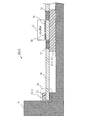
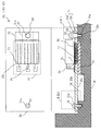
- FIG. 1 is a cross-sectional view of the power supply device 100-1. Note that the electric component 25 and the screw do not show a cross section.
- FIG. 1 shows an xyz coordinate system. Embodiments 2 to 9 also show the same coordinate system.
- FIGS. 4 and 6 to 14 which are cross-sectional views of the second to ninth embodiments show the same cross-section as that of FIG.
- the power supply device 100-1 includes the chassis 10, a board 20 on which the electric components 25 are mounted and fixed to the chassis 10, and a fixing unit 30 for fixing the board 20 to the chassis 10.
- the fixing portion 30 is a substrate fixing screw 31.
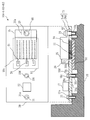
- FIG. 2 shows a partial plan view of the chassis 10 (viewed in the direction of the arrow -Z in FIG. 1) and a cross section taken along the line EE. The EE cross section corresponds to FIGS.
- a board fixing screw 31 is screwed into the screw hole 12.
- FIG. 1 illustrates a part of the chassis 10 and the substrate 20.
- the chassis 10 has a plurality of screw holes 12.
- a board fixing screw 31 is screwed into each screw hole 12.
- FIG. 3 is a diagram schematically showing a portion corresponding to the range 13 in FIG. 2, that is, an arrow view when FIG. 1 is viewed from the ⁇ Z direction.
- the board 20 on which the electric components 25 are mounted is fixed to the chassis 10.
- the electrode 26 of the electric component 25 is connected to the C surface which is the other surface 20b of the back surface of the one surface 20a of the substrate 20.
- a filling through hole 21 described later is formed in the substrate 20.
- FIG. 1 shows ten filled through holes 21. The heat 8 generated by the electric component 25 indicated by the arrow is transmitted from the filling through hole 21 to the chassis surface 11 via a cured insulating resin 27-1 described later.
- the power supply device 100-1 includes the board 20, the chassis 10, and the cured insulating resin 27-1, which is the chassis-side resin portion 91, and the electric component 25 is mounted on the board 20.
- the chassis 10 has a chassis surface 11 which is a surface facing one surface 20a of the substrate 20.
- the cured insulating resin 27-1 is disposed between one surface 20a of the substrate 20 and the chassis surface 11.
- the cured insulating resin 27-1 is a cured insulating resin connected to one surface 20a and the chassis surface 11 and having a thermal conductivity of 1 W / mK or more and 10 W / mK or less.
- An electric component 25 that generates a large amount of heat is attached to the substrate 20.
- an SMD (Surface Mount Device) type FET is used as the electric component 25 having a large heat value. Normally, heat generated in the SMD type FET is transmitted from the electrode of the FET to the circuit pattern of the substrate 20, transmitted in an in-plane direction, and transmitted to the chassis 10 via the screw portion.
- the S surface, which is one surface 20a of the substrate 20, and the chassis 10 are made of an insulating resin composition having high thermal conductivity (insulating resin cured product 27-1 before curing). Is potted (molded) with the chassis surface 11. Thereby, the heat of the electric component 25 is transmitted to the chassis 10 through the high thermal conductive potting resin which is an insulating resin composition.
- a through hole penetrating from the C surface to the S surface of the substrate 20 is provided. .
- the through holes are plated.
- the inside of the plated through hole is filled with solder, other metal, or a potting resin having high thermal conductivity. This through hole is called a filled through hole 21.
- the substrate 20 includes the filled through-hole 21 in which the through-hole penetrating from the one surface 20a to the other surface 20b is filled with the heat transfer material.
- the cured insulating resin 27-1 is connected to one end 21a of the filling through hole 21 that appears on one surface 20a.
- the heat transfer material filled in the filling through hole 21 is a metal and a cured insulating resin having a thermal conductivity of 1 W / mK or more and 10 W / mK or less.
- the cured insulating resin 27-1 silicone or urethane is used as a base resin.
- the cured insulating resin 27-1 contains at least one of alumina, boron nitride, aluminum nitride, magnesium oxide, and beryllium oxide as an inorganic filler, and the cured insulating resin 27-1 has a hardness of Shore.
- the hardness of A is 70 or less
- the volatilization amount of the low-molecular component when heated at 300 ° C. is 1000 ppm or less
- the glass transition point is ⁇ 20 ° C. or less.
- a liquid insulating resin composition is poured between the chassis 10 and the substrate 20, and the insulating resin composition is cured by heating.
- the substrate 20 is fixed to the chassis 10 with the substrate fixing screws 31.
- the thickness L2 of the cured insulating resin 27-1 before attaching the substrate 20 to the chassis 10 depends on the hardness of the cured insulating resin 27-1.
- the thickness of the cured insulating resin 27-1 is less than 110% of the width between the S surface and the chassis surface 11, That is, L2 ⁇ 1.1 ⁇ L1
- the thickness of the cured insulating resin 27-1 is reduced by the cooling / heating cycle, so that the heat discharging effect is reduced.
- the thickness L2 exceeds 200% of the thickness L1, That is, L2> 2.0 ⁇ L1
- the substrate 20 is deformed when the substrate 20 is fixed to the chassis 10 with screws, and the deformation may cause a crack in the substrate 20 in a cooling / heating cycle.
- the liquid insulating resin composition may be poured with the S surface of the substrate 20 facing upward (+ Z direction) to form the cured insulating resin 27-1. . Also in this case, the thickness L2 of the cured insulating resin is set to the thickness described in the above (2).
- the substrate 20 is fixed to the chassis 10 with screws so that the formed insulating resin cured product 27-1 and the chassis 10 are in contact with each other. By doing so, no bubbles serving as insulation weak points remain in high-voltage portions such as a wiring pattern on the S surface.
- the hardness of the cured insulating resin 27-1 obtained by curing the liquid insulating resin composition is 80 or less (Shore A), and more preferably 70 or less.
- the hardness is indicated by a Shore A hardness meter as a representative.
- a soft material may be measured by Shore E, Shore 00, ASKER C, or the like. If the shore A is 80 or less, the measurement may be performed by Shore E, Shore 00, or ASKER C.
- the cured insulating resin 27-1 is finely cut, and the components of the cured insulating resin 27-1 are extracted with an organic solvent such as hexane or acetone.
- the amount of low molecular components is analyzed using a gas chromatograph mass spectrometer (GC / MS) while elevating the temperature of the extraction solvent from 40 ° C. to 300 ° C. using helium as a carrier gas. Its low molecular component content is 2000 ppm or less, preferably 1000 ppm or less.
- Insulation resin cured product 27-1 was tested in a vacuum environment (7 ⁇ 10 ⁇ 3 Pa or less) at a heating temperature of 125 ° C., a holding time of 24 hours, and a discharge gas cooling temperature of 25 ° C. in accordance with ASTM E595. Test under the conditions. Under these test conditions, the outgas released from the cured insulating resin 27-1 is measured.
- the mass loss ratio (TML: Total Mass Loss) calculated from the measurement results should be 1% or less, and the recondensable substance amount ratio (CVCM: Collected Volatile Condensable Material) should be 0.1% or less.
- TML Total Mass Loss
- CVCM Collected Volatile Condensable Material
- the glass transition point of the cured insulating resin 27-1 is ⁇ 10 ° C. or lower, preferably ⁇ 20 ° C. or lower. More preferably, the temperature is lower than the low-temperature side of the cooling / heating cycle temperature when the cured insulating resin 27-1 is used.
- the glass transition point is higher than ⁇ 10 ° C., there is a fear that in the cooling and heating cycle when the cured insulating resin 27-1 is used, the deformation of the cured insulating resin 27-1 becomes large and stable exhaust heat cannot be obtained, or There is a possibility that the substrate 20 may be warped.
- liquid insulating resin a liquid thermosetting resin such as a silicone resin or a urethane resin can be used.
- silicone resin (Silicone resin)
- Known silicone resins can be used as long as they are liquid at room temperature.
- the curing system of the silicone resin may be either an addition reaction type or a condensation reaction type.
- the silicone resin may be in the form of a rubber (elastomer) or gel after curing.
- the base polymer is a liquid having an average molecular weight of 5,000 to 100,000 and a viscosity at 25 ° C. of 1 to 100,000 Pa ⁇ s.
- the base polymer has a linear, cyclic, branched or ladder-like main chain having at least one kind of an alkyl group, an alkenyl group, an allyl group, a hydroxyl group, a hydrogen group, an alkoxyalkyl group, and an alkoxysilyl group at a side chain and a terminal. It is a known organopolysiloxane having a structure.
- the base polymer may be a mixture of two or more organopolysiloxanes.
- a composition containing an organopolysiloxane containing an alkenyl group as a base polymer, a hydrogen siloxane as a crosslinking agent, and a platinum compound as a catalyst can be used.
- These compounding amounts may be known effective amounts since the curing reaction proceeds and a required hardness is obtained after curing.
- a composition containing an organopolysiloxane containing a silanol group as a base polymer, a silane compound such as alkoxysilane or acetoxysilane as a crosslinking agent, and an organotin compound as a catalyst can be used.
- the amount of these components may be a conventionally known effective amount because the curing reaction proceeds and a required hardness is obtained after curing.
- the urethane resin has a urethane bond in a composition obtained by combining a polyol resin having a plurality of hydroxyl groups in one molecule as a main component and a compound having two or more isocyanate groups in one molecule as a curing agent and copolymerizing them. It is a resin having.
- a known resin can be used as long as the viscosity at 25 ° C. after mixing is 1 to 100,000 Pa ⁇ s.
- polystyrene resin known polyester-based polyols, dicarboxylic acid ester-based polyols, polyether-based polyols, polytetramethylene polyoxyglycol, castor oil-based polyols, ⁇ -caprolactone-based polyols, polyoxypolyalkylene-based polyols, ⁇ - Methyl- ⁇ -valerolactone-based polyols, carbonate-based polyols and the like may be used, and two or more of these may be used in combination.
- isocyanate compound known tolylene diisocyanate, naphthalene diisocyanate, hexamethylene diisocyanate, xylidene diisocyanate, diphenylmethane diisocyanate, isophorone diisocyanate, cyclohexyl diisocyanate, or the like may be used, or two or more of these may be used in combination.
- an appropriate urethanization catalyst can be used.
- catalysts such as tertiary amine compounds and organometallic compounds can be used as the urethanization catalyst.
- urethanization catalyst examples include triethylenediamine, N, N′-dimethylhexamethylenediamine, N, N′-dimethylbutanediamine, diazabicyclo (5,4,0) undecene-7 (DBU) and DBU salt, and octylic acid.
- DBU diazabicyclo (5,4,0) undecene-7
- octylic acid examples include lead, dibutyltin laurate, bismuth tris (2-ethylhexanoate), diisopropoxybis (ethylacetoacetate) titanium, and the like.
- the blending of the polyol and the isocyanate compound is calculated from the equivalent ratio of the isocyanate group (NCO) of the isocyanate to the hydroxyl group (OH) of the polyol.
- the equivalent ratio (NCO / OH) is not particularly limited, but is preferably in the range of 0.95 to 1.05. If the equivalent ratio exceeds 1.05, the hardness of the cured product of the insulating resin composition is undesirably high. Further, voids remain in the cured product due to the by-product carbon dioxide, which is not preferable because the insulating properties are deteriorated. On the other hand, if the equivalent ratio is less than 0.95, the progress of the curing reaction is slow and uncured material tends to be produced, which is not preferable because production stability is lacking. Further, it is not preferable because of lack of heat resistance.
- the filler having thermal conductivity has a role of imparting thermal conductivity to the composition (cured product), and a known thermal conductive filler can be used.
- a filler for example, alumina powder, magnesium oxide powder, boron nitride powder, aluminum nitride powder, beryllium oxide powder, zinc oxide powder, silicon nitride powder, silicon oxide powder, aluminum powder, copper powder, silver powder, nickel powder, gold Powder, diamond powder, carbon powder, indium, gallium and the like.
- alumina powder magnesium oxide powder, boron nitride powder, aluminum nitride powder, beryllium oxide powder, silicon oxide powder. It is preferable to use a powder having a high insulating property.
- Such a heat conductive filler may be used alone or in combination of two or more.
- the thermal conductive filler preferably has a thermal conductivity of 10 W / m ⁇ K or more. If the thermal conductivity is less than 10 W / m ⁇ K, the composition (cured product) cannot have sufficient thermal conductivity.
- the average particle size of the filler for imparting thermal conductivity is 0.1 ⁇ m or more and 200 ⁇ m or less, Preferably, It is 0.5 ⁇ m or more and 100 ⁇ m or less.
- Such a thermally conductive filler having an average particle size may be used alone or as a mixture of two or more kinds having different particle sizes.
- a thermally conductive filler having an average particle size of less than 0.1 ⁇ m is not preferred because the particles are likely to aggregate and have poor fluidity.
- a thermally conductive filler having an average particle size of more than 100 ⁇ m is not preferred because the particles are likely to settle and the thermal conductivity of the cured product may be non-uniform.
- the shape of the filler may be irregular, spherical, or any shape.
- the average particle diameter can be measured as a volume average value D50 (that is, a particle diameter or a median diameter when the cumulative volume becomes 50%) in the particle size distribution measurement by a laser light diffraction method.
- the insulating resin composition is obtained by mixing the above-mentioned liquid insulating resin with the above-mentioned inorganic filler for imparting high thermal conductivity.
- the thermal conductivity of the cured product increases.
- the viscosity of the composition increases, the workability decreases, or the hardness of the cured product increases, so that the adhesion to the substrate decreases. Due to these factors, there is a possibility that the intended exhaust heat effect cannot be obtained. Therefore, the mixing ratio of the inorganic filler contained in the liquid insulating resin composition is not particularly limited as long as the viscosity at 25 ° C.
- the insulating resin composition containing the inorganic filler is 300 Pa ⁇ s or less. Further, when it is necessary to pour the insulating resin composition into a narrow gap, its viscosity is desirably 50 Pa ⁇ s or less.
- the inorganic filler is 40 vol% or more and 80 vol% or less, Is preferably included in the range of, 50 vol% or more and 75 vol% or less, More preferably, it is included in the range. If the content exceeds 80 vol%, the viscosity of the insulating resin composition is increased and the workability is deteriorated, or the hardness of the cured product is increased, and stable exhaust heat characteristics cannot be obtained.
- a reaction control agent such as an acetylene compound, various nitrogen compounds, an organic phosphorus compound, an oxime compound, and an organic chloro compound, or silane coupling, for controlling the reactivity of the insulating resin composition and the adhesion to the base material.
- An additive such as an adhesion modifier such as an agent may be appropriately added as needed.
- the curing condition of the liquid insulating resin composition can be the same as that of a known silicone potting material or urethane potting material.
- the curing temperature is From room temperature to 180 ° C or less is good, More preferably, the temperature is from room temperature to 150 ° C. or lower. When the curing temperature is lower than room temperature, the curing is insufficient, and unreacted raw materials are volatilized in a cooling and heating cycle during use, which may contaminate the electric parts. On the other hand, if the curing temperature exceeds 150 ° C., the temperature may exceed the heat resistance temperature of the electric component, and the electric component may be deteriorated.
- the curing time is not limited as long as the required hardness is obtained, 48 hours or less at room temperature, preferably 24 hours or less, In the case of heat curing, 0.1 hours or more and 12 hours or less, Preferably, it is 0.5 hours or more and 6 hours or less. If there is a concern about outgassing when using the cured insulating resin 27-1, it is preferable to heat and cure. For example, if the heat treatment is performed at the upper limit of the allowable temperature for use of the electric component, the volatile components in the cured product that are easily volatilized can be reduced, and the adverse effect of the outgas can be avoided.
- the dielectric breakdown electric field of the cured product of the insulating resin composition is It is preferably 10 kV / mm or more, more preferably 15 kV / mm or more. In the case of less than 10 kV / mm, the distance between the wiring of the electric components and the distance between the wiring patterns of the substrate 20 need to be increased depending on the used voltage, and the contribution of the miniaturization of the power supply member is reduced.
- the volume resistivity of the cured product of the insulating resin composition is 1.0E + 10 ⁇ ⁇ cm or more is preferable, and more preferably 1.0E + 12 ⁇ ⁇ cm or more. In the case of less than 1.0E + 10 ⁇ ⁇ cm, it is necessary to increase the distance between the wiring of the electric components and the wiring pattern of the substrate 20 depending on the working voltage, and the contribution of the miniaturization of the power supply member is reduced.
- a surface modifier for improving adhesion. No problem.
- Known silicone or urethane primers can be used.
- the method of pouring a resin between the substrate 20 and the chassis 10 is as follows.
- the method of manufacturing the power supply device 100-1 is as follows.
- the liquid resin composition uses silicone or urethane as a base resin, and contains at least one of alumina, boron nitride, aluminum nitride, magnesium oxide, and beryllium oxide as an inorganic filler.
- the hardness of the chassis side resin portion 27-1 is preferably 70 or less in Shore A hardness. It is preferable that the chassis-side resin portion 27-1 has a volatilization amount of low-molecular components at 300 ° C. of 1000 ppm or less and a glass transition point of -20 ° C. or less.
- the outline of the method of manufacturing the power supply device 100-1 for attaching the substrate 20 to the chassis 10 after curing the resin is as follows.
- the method of manufacturing the power supply device 100-1 is as follows. A pouring step of pouring an insulating liquid resin composition into the chassis surface 11, A curing step of curing the liquid resin composition poured into the chassis surface 11 to generate the chassis-side resin portion 91; A mounting step of mounting the substrate 20 to the chassis 10 such that one surface 20a of the substrate 20 faces the chassis surface 11 and is in close contact with the chassis-side resin portion 91.
- the liquid resin composition is Silicone or urethane is used as a base resin, and at least one of alumina, boron nitride, aluminum nitride, magnesium oxide, and beryllium oxide is contained as an inorganic filler.
- the hardness of the chassis side resin portion 27-1 is preferably 70 or less in Shore A hardness. It is preferable that the chassis-side resin portion 27-1 has a volatilization amount of low-molecular components at 300 ° C. of 1000 ppm or less and a glass transition point of -20 ° C. or less.
- the viscosity of the liquid resin composition at 25 ° C. is preferably 300 Pa ⁇ s or less.
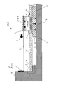
- FIG. 4 is a sectional view of the power supply device 100-2.
- FIG. 5 is a diagram corresponding to FIG. 3 and is a schematic diagram corresponding to the -Z direction arrow in FIG.
- the power supply device 100-2 uses an electric component 25 having a lead as an electrode 26, such as a TO-254 package, as a power MOSFET for space, with respect to the power supply device 100-1.
- the electric component 25 that is a heat generating component is TO-254.
- the power supply device 100-2 differs from the power supply device 100-1 in the following (1) to (3). Others are the same as the power supply device 100-1.
- Filled through-holes 21 are provided directly below the electric components 25 to transfer heat to the S surface of the substrate 20.
- a heat conducting material 23 is disposed between the lower surface of the electric component 25 and the substrate 20 in order to efficiently transfer the heat 8 of the electric component 25 to the filling through hole 21.
- the heat conductive material 23 is, for example, a solder paste or a silver paste.
- the electric component 25 is fixed to the board 20 with fixing screws 29.
- the same type of electric component 25 used for space is designed to have a heat dissipation design in which a semiconductor is mounted in a position near the surface in contact with the substrate 20 or the chassis 10 or the like within the electric component 25 (in the package). I have. Therefore, by adopting the configuration of FIG. 4, heat can be efficiently exhausted to the chassis 10.
- filling the through holes with solder or other metal or heat conductive resin, and pouring a resin having a high heat conductivity between the S surface of the substrate 20 and the chassis 10 are: This is the same as in the first embodiment.
- FIG. 6 is a diagram illustrating the power supply device 100-3.
- the power supply device 100-3 has a configuration in which the head of the substrate fixing screw 31 is potted with respect to the power supply device 100-1 with a resin 27-2 having high thermal conductivity.
- the other configuration of the power supply device 100-3 is the same as that of the power supply device 100-1.
- the chassis 10 has a plurality of screw holes 12, and when the substrate fixing screws 31 are screwed into these screw holes 12, the heads of the substrate fixing screws 31 It may be configured to be covered with the resin 27-2.
- the board fixing screws 31 and the screw holes 12 are arranged in plural at the peripheral portion along the outer periphery of the board 20, and are provided at, for example, four corners or four sides of a rectangle at predetermined intervals.
- FIG. 7 and 8 are diagrams showing a power supply device 100-4 according to the fourth embodiment.
- the power supply device 100-4 in FIGS. 7 and 8 is the same as the power supply device 100-1, except that the configuration of the fixing unit 30 is different from the power supply device 100-1.
- the power supply device 100-4 shown in FIG. 7 has a configuration in which a spring fixture 33 having spring characteristics is provided between the board 20 and the chassis 10.
- the thermal expansion coefficient of the cured insulating resin 27-1 is several hundred ppm, which is larger than several ppm to several tens ppm of metal. Therefore, when the insulating resin cured material 27-1 filled between the chassis 10 and the substrate 20 changes in dimensions such as thickness and width due to heat, the substrate 20 is also moved by the spring fixing member 33. 1 can be followed. Therefore, separation between the substrate 20 and the cured insulating resin 27-1 can be suppressed.
- the substrate 20 and the spring fixing member 33 are connected by solder 32a, but may be fastened by screws 32b as in the power supply device 100-4 of FIG.
- a plurality of the board fixing screws 31 and the spring fixing tools 33 are arranged at a peripheral portion along the outer periphery of the board 20, and are provided at predetermined intervals at, for example, four corners or four sides of a rectangle.
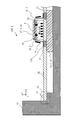
- FIG. 9 is a diagram illustrating a power supply device 100-5 according to the fifth embodiment.
- the power supply device 100-5 differs from the power supply device 100-1 in the following (1) to (3). Others are the same as the power supply device 100-1.
- the electrode 26 of the electric component 25 is on the electric component 25.
- the electrode 26 and the filling through-hole 21 are connected by a wire or a bus bar, which is the electrode connecting portion 28-1.
- the electric component 25 is fixed to the substrate 20 with the adhesive 24.
- the electrode 26 is directly connected to a circuit pattern on the substrate 20.
- the electrode 26 of the electric component 25 is deliberately directed upward in the opposite direction to the substrate 20, and a wire or bus bar is connected to the electrode 26 facing upward as an electrode extension, and the wire or bus bar is connected to the circuit of the substrate 20.
- the method of connecting to the pattern is taken. In such a case, it is possible to connect a wire or a bus bar to the filling through hole 21 to exhaust heat.
- a wire or a bus bar is used as the electrode connecting portion 28-1, which is a heat transfer material for connecting the electrode 26 and the filling through hole 21, for the purpose of exhausting heat.
- FIG. 10 is a diagram illustrating a power supply device 100-6 according to the sixth embodiment.
- the power supply device 100-6 has a configuration in which the electric component 25 and the electrode connection portion 28-1 that is a bus bar or a wire are further wrapped in a cured resin 27-3 with respect to the power supply device 100-5. With this configuration, the thermal conductivity can be improved.
- the cured resin 27-3 is the component-side resin portion 92.
- the filling through hole 21 is arranged at any position around the electric component 25 on the substrate 20.
- the cured resin 27-3 is arranged at a position opposite to the cured insulating resin 27-1 with respect to the substrate 20 so that the substrate 20 is sandwiched between the cured resin 27-3 and the cured insulating resin 27-1 as the chassis-side resin portion 91. Have been.
- the resin cured product 27-3 is an insulating resin cured product that seals the electrical component 25, the other end 21b of the filling through hole 21 that appears on the other surface 20b of the substrate 20, and the electrode connection portion 28-1. It is.
- the cured resin 27-3 the same resin as the cured insulating resin 27-1 can be used.
- FIG. 11 and 12 are diagrams showing a power supply device 100-7 according to the seventh embodiment.
- the power supply device 100-7 shown in FIG. 11 has a configuration in which a bus bar for exhausting heat, which is the chassis connection portion 28-2, is provided above the electric component 25 with respect to the power supply device 100-6. Chassis connection portion 28-2 is fixed to chassis 10 with screws 42. The exhaust heat can be increased by the bus bar for exhaust heat.
- the cured resin 27-3 in FIG. 11 is a contact resin portion 93 which is a cured insulating resin.
- FIG. 12 shows a configuration in which the cured resin 27-4, which is the contact resin portion 93, is disposed above the electric component 25.
- the electric component 25 shown in FIG. 12 has the same electrodes 26 as the electric component 25 shown in FIG. 13 described later, but the direction in which the electrodes 26 are arranged is the Y direction in FIG. 12 and the X direction in FIG.
- the same resin as the cured insulating resin 27-1 can be used as the cured resin 27-4.
- heat can also be discharged from the upper part of the electric component 25 whose upper side opposite to the substrate 20, such as an SMD type transformer or IC, is molded with the cured resin 27-4.
- the contact resin portion 93 and the cured insulating resin 27-1 as the chassis-side resin portion 91 sandwich the substrate 20 therebetween.
- Contact resin portion 93 is arranged at a position opposite to cured insulating resin 27-1 with respect to substrate 20, and comes into contact with at least a part of electric component 25.
- Chassis connecting portion 28-2 having heat conductivity connects contact resin portion 93 and chassis 10.
- FIG. FIG. 13 is a diagram illustrating a power supply device 100-8 according to the eighth embodiment.
- the chassis connection portion 28-2 which is a bus bar provided for exhaust heat, is connected to the chassis 10.
- the through-hole connection portion 28-3 is connected to the other end 21b of the filling through-hole 21 on the substrate 20.
- the heat 8 is exhausted to the chassis 10 via the cured insulating resin 27-1. Therefore, the heat exhaust path can be shorter than that of the power supply device 100-7 in FIG.
- the filling through hole 21 is arranged at any position around the electric component 25 on the substrate 20.
- the contact resin portion 93 and the cured insulating resin 27-1 as the chassis side resin portion 91 sandwich the substrate 20 therebetween.
- Contact resin portion 93 is arranged at a position opposite to cured insulating resin 27-1 with respect to substrate 20, and comes into contact with at least a part of electric component 25.
- the through-hole connecting portion 28-3 connects the contact resin portion 93 and the other end 21b of the filled through-hole 21.
- Embodiment 9 shows a ninth embodiment.
- Embodiment 9 relates to a method of manufacturing the power supply device 100 in an environment where air exists.
- the operation of forming a layer of the cured insulating resin 27-1 (insulating resin composition) between the substrate 20 and the chassis 10 in a normal air environment on the ground, not in a vacuum, 4 shows an operation of injecting an insulating resin composition.
- the power supply device 100-8 is taken as an example, but the method of the ninth embodiment can be applied to the power supply devices 100-1 to 100-7.
- FIG. 14 shows a preferable manufacturing method in an atmospheric environment
- FIG. 14B shows an unfavorable manufacturing method in an atmospheric environment.
- the flow of air is indicated by an arrow 44.
- FIG. 14A air bubbles go out of the liquid insulating resin composition in the Z direction, which is upward, because of the difference in specific gravity between the liquid insulating resin composition and the air bubbles, that is, air. become. Therefore, the probability of entraining air is reduced.
- FIG. 14B the air flowing upward, that is, in the Z direction is blocked by the S surface of the substrate 20, and the void 41 is easily formed.
- the formation of the voids 41 which are usually easily formed on the S-plane of the substrate 20 even in the air and which lowers the thermal conductivity can be avoided as much as possible. It is possible. As a result, the resin layer can be formed without placing the device in a vacuum vessel, and workability is greatly improved. In addition, costs associated with equipment introduction can be reduced.
- the power supply device 100 described in the first to ninth embodiments has a high thermal conductivity that can withstand the space environment between the S surface of the substrate on which the high heat generation component is mounted and the chassis of the power supply connected to the structure of the artificial satellite. Potting (filling and molding) with a liquid insulating resin having a high thermal conductivity, and potting (filling and molding) with a liquid insulating resin having a high thermal conductivity that can withstand the space environment, and the screw part connecting the board and the chassis , Ensure a heat removal path.
- the above-described heat dissipation path is provided to increase the heat dissipation ability to the chassis which is the housing of the power supply. By increasing, it is possible to suppress a rise in the temperature of components on the substrate.
- the above-mentioned liquid insulating resin having high thermal conductivity contains at least one of alumina, boron nitride, aluminum nitride, magnesium oxide, and beryllium oxide as an inorganic filler imparting high thermal conductivity.
- the hardness of the cured liquid insulating resin is 70 or less (Shore A).
- the cured product of the liquid insulating resin has a volatilization amount of the low molecular component of 500 ppm or less when heated at 300 ° C. and a glass transition point of ⁇ 20 ° C. or less.
- the cured product of the liquid insulating resin is silicone or urethane as the base resin.
- Embodiment 10 FIG. The tenth embodiment will be described with reference to FIGS.
- power supply devices 101-1, 101-2, 102-1, 102-2, 102-3, and 102-4 will be described.
- the tenth embodiment relates to a power supply device that holds the potential of the ground terminal 25a of the electrical component 25 and the potential of the chassis 10 at different potentials, and transmits the heat of the electrical component 25 to the chassis 10.
- chassis 10 has an upright portion.
- FIG. 15 shows a plan view and a sectional view of the power supply device 101-1.
- the upper part of FIG. 15 schematically shows a plan view of the power supply device 101-1 in the Z1 direction.
- the filled through holes 21 are indicated by solid lines.
- the power supply device 101-1 according to the tenth embodiment will be described with reference to FIG.
- the power supply device 101-1 includes a chassis 10, a substrate 20, and a chassis-side resin portion 91.
- the one surface 20a and the other surface 20b of the substrate 20 are hereinafter referred to as a surface 20a and a surface 20b.
- An electric component 25 is mounted on the board 20.
- the chassis 10 includes a chassis surface 11 which is a surface facing the surface 20a of the substrate 20, and a surface 20a which rises from the chassis surface 11 toward the surface 20a and whose end 14a in the rising direction 15 does not contact the surface 20a.
- the upright section 14 is a heat transfer section 94. The heat generated in the electric component 25 is transmitted to the upright portion 14.
- the chassis-side resin portion 91 is disposed between the surface 20a of the substrate 20 and the end 14a of the upright portion 14, and is connected to the surface 20a and the end 14a.
- the chassis-side resin portion 91 is a cured insulating resin having a thermal conductivity of 1 W / mK or more and 10 W / mK or less.
- the substrate 20 has a filled through hole 21 in which a heat transfer material is filled in a through hole penetrating from the surface 20a to the surface 20b.
- the chassis-side resin portion 91 is connected to one end 21a of the filling through hole 21 appearing on the surface 20a and the end 14a of the upright portion 14.
- the heat transfer material of the filled through hole 21 is either a metal or a cured insulating resin having a thermal conductivity of 1 W / mK or more and 10 W / mK or less.
- the chassis 10 has a mounting portion 16 and a standing portion 14 which is a heat transfer portion 94.
- the ground terminal 25 a of the electric component 25 is fixed to the mounting portion 16 together with the electric component 25 by a fixing screw 29.
- the ground terminal 25a is thermally connected to the filling through hole 21.
- the chassis 10 has an insulator 17, and the electric component 25 is fixed to the insulator 17 with fixing screws 29. Specifically, the fixing screw 29 is engaged with the female screw 18 formed on the insulator 17 embedded in the chassis 10. As shown in FIG. 15, the filling through hole 21 is not in contact with the fixing screw 29.
- the upright portion 14 has an end surface 14 b of the end portion 14 a protruding from the chassis surface 11, and the end surface 14 b is close to the surface 20 a of the substrate 20.
- the chassis-side resin portion 91 is filled between the end surface 14 b of the upright portion 14 and the surface 20 a of the substrate 20.
- the chassis-side resin portion 91 is thermally connected to the filling through hole 21 that is thermally connected to the electric component 25.
- the periphery of the filling through hole 21 is surrounded by the non-conductive region 20 c of the substrate 20.
- the non-conductive region 20c is a non-conductive region on the substrate 20.
- the creepage distance d1 of the non-conductive region 20c is longer than a predetermined distance d from the ground terminal 25a.
- the creeping distance d1 along the surface 20a between the end of the ground terminal 25a and the side surface 14c of the upright portion 14 is equal to or longer than the predetermined distance d.
- the high-voltage electric component 25 can be attached to the board 20.
- the potential of the electrode 26 of the electric component 25 and the potential of the ground terminal 25 a are different from those of the chassis 10.
- the power supply device 101-1 shown in FIG. 15 has a configuration in which the chassis 10 provided with a step by the upright portion 14 and the filling through hole 21 provided in the substrate 20 are filled with a chassis side resin portion 91.
- This configuration has a feature that the filling through hole 21 is connected to “the side surface 14 d of the upright portion 14 and the end surface 14 b of the upright portion 14, which are the wall surfaces of the step”.
- the heat 8 of the electric component 25 is transmitted from the filling through hole 21 of the board 20 to the chassis-side resin portion 91, and is transmitted from the chassis-side resin portion 91 to the upright portion 14 of the chassis 10. Further, the heat 8 of the electric component 25 is transmitted from the periphery of the fixing screw 29 to the mounting portion 16 via the substrate 20.
- the heat discharge performance largely depends on the thermal conductivity of the resin.
- a raised step is provided on the chassis 10 by the upright portion 14.
- a concave portion 55 having a concave shape is provided in the chassis 10.
- FIG. 16 shows a power supply device 101-2 which is a modification of the power supply device 101-1.
- the electric component 25 is covered with the component-side resin portion 92. This is the only difference from the power supply device 101-1.
- a configuration in which the electric component 25 is covered with the component-side resin portion 92 may be employed.
- FIG. 17 shows a plan view and a sectional view of the power supply device 102-1.
- the upper part of FIG. 17 schematically shows a plan view of the power supply device 102-1 in the Z1 direction.
- the positions of the end face 14b of the upright portion 14-1 and the plurality of filling through holes 21 are shown.
- the filled through holes 21 are indicated by solid lines.
- the substrate 20 includes a filled through hole 21 in which a through hole penetrating from the surface 20a to the surface 20b is filled with a heat transfer material.
- the upright portion 14-1 stands upright from the chassis surface 11 toward the surface 20a inside the chassis-side resin portion 91, and the end 14a in the upright direction 15 faces the surface 20a.
- the chassis-side resin portion 91 is connected to one end 21a of the filling through hole 21 that appears on the surface 20a.
- the end surface 14b of the upright portion 14-1 is in contact with the non-conductive region 20c on the surface 20a of the substrate 20. That is, the end surface 14b of the end 14a of the upright portion 14-1 is in contact with the non-conductive region 20c.
- a region where one end 21a of the filled through hole 21 does not appear on the surface 20a is a non-conductive region 20c.
- the upright portion 14-1 has, for example, a columnar shape.
- the upright portion 14-1 has, for example, a columnar shape, a triangular prism shape, a quadrangular prism shape, or a polygonal prism shape having five or more angles.
- a plurality of filling through holes 21 are arranged around the non-conductive region 20c. As shown in the upper diagram of FIG. 17, the non-conductive region 20c is surrounded by a plurality of filling through holes 21.
- electric components 25 are arranged on the plurality of filling through holes 21.
- the upright portion 14 is surrounded by the chassis-side resin portion 91.
- the end surface 14b of the upright portion 14 is in contact with the surface 20a of the substrate 20, but the gap between the end surface 14b and the surface 20a of the substrate 20 may be filled with the chassis-side resin portion 91.
- the creepage distance d1 along the surface 20a between the end of the end surface 14b of the upright portion 14 and the nearest filling through hole 21 is the predetermined distance d as in the case of the power supply device 101-1. It is more than the length. This is the same for the power supplies 102-2, 102-3, and 102-4.
- FIG. 18 is a cross-sectional view of the power supply device 102-2.
- FIG. 19 is a sectional view of the power supply device 102-3.
- FIG. 20 is a sectional view of the power supply device 102-4.
- the power supply device 102-2, the power supply device 102-3, and the power supply device 102-4 are different from the power supply device 102-1 in the shape of the upright portion.
- Both the upright portion 14-2 of the power supply device 102-2 and the upright portion 14-4 of the power supply device 102-4 change their cross-sectional shapes with the upright direction 15 as the normal line toward the upright direction 15. are doing. In the upright portion 14-2 and the upright portion 14-4, the cross-sectional shape gradually decreases in the upright direction 15.
- the cross-sectional area (outer diameter) of the upright portion 14-2 of the power supply device 102-2 changes.
- the upright portion 14-2 of the power supply device 102-2 gradually decreases in cross-sectional area from the chassis surface 11 to the surface 20a of the substrate 20.
- the upright portion 14-2 of the power supply device 102-2 has a shape in which a plurality of columns having different outer diameters are stacked in order from the chassis surface 11 to the surface 20a of the substrate 20 in order of increasing outer diameter.
- the outer diameter of the cross-sectional area changes from the chassis surface 11 to the surface 20a by repeating a major axis and a minor axis.
- the upright portion 14-3 has a spiral shape or a wedge-shaped vertical cross section, and has an uneven outer periphery.
- the cross-sectional area of the upright portion 14-4 of the power supply device 102-4 decreases gradually or continuously from the chassis surface 11 toward the surface 20a of the substrate 20.
- the standing portion 14-4 has a truncated cone shape or a truncated polygonal pyramid shape.
- the chassis-side resin portion 91 connects the end surface 14b of the upright portion 14 and the surface 20a.
- the creepage distance d1 is a length equal to or longer than the predetermined distance d. Therefore, according to the power supply devices 101-1 and 101-2, the potential of the ground terminal 25a and the potential of the chassis 10 are maintained at different potentials, and the heat of the electric component 25 is transmitted to the chassis 10. Can be.
- the end surface 14b of the upright portion 14 is in contact with the surface 20a.
- the chassis-side resin portion 91 connects the end surface 14b of the upright portion and the surface 20a.
- the creepage distance d1 is a length equal to or longer than the predetermined distance d. Therefore, according to the power supply devices 102-1 to 102-4, the potential of the ground terminal 25a and the potential of the chassis 10 are maintained at different potentials, and the heat of the electric component 25 is transmitted to the chassis 10. Can be.
- FIG. FIG. 21 shows a power supply device 103 according to the eleventh embodiment.
- a step is provided with respect to the chassis surface 11, and a concave portion 55 is present.
- the concave portion 55 is indicated by corners A to D in FIG.
- the recess 55 has a bottom surface 11 a lower than the chassis surface 11.
- the power supply device 103 includes an electric component 25, a substrate 20, a chassis 10 having a chassis surface 11 facing the surface 20 a of the substrate 20, and a chassis-side resin portion 91.
- the board 20 has a solder leveler forming region 51 in which a solder leveler 54 is formed in a region of the surface 20b which is the back surface of the surface 20a and is covered with the electric component 25, and the solder leveler 54 is formed in the surface 20a. It has a solder leveler formation region 51.
- the substrate 20 has a plurality of through holes 52 that penetrate from the surface 20a to the surface 20b, and are disposed in a region where the solder leveler 54 is formed on the inner surface and is covered with the electric component 25.
- the chassis-side resin portion 91 is formed between the electric component 25 and the solder leveler forming region 51 formed on the surface 20 b of the board 20 and between the solder leveler forming region 51 formed on the surface 20 a of the board 20 and the chassis 10. And inside the through hole 52.
- the chassis-side resin portion 91 has a thermal conductivity of 1 W / mK or more and 10 W / mK or less, and a hardness of 70 or less on a Shore A hardness meter.
- the chassis-side resin portion 91 is an insulating resin cured product.
- the solder leveler 52a formed in the through hole 52 is connected to the solder leveler forming region 51 formed on the surface 20a and the solder leveler forming region 51 formed on the surface 20b.
- the power supply device 103 is characterized in that, as described above, the chassis-side resin portion 91 which is a cured resin is provided at the locations described in (1), (2), and (3) below. Is arranged.
- the chassis-side resin portion 91 has a thermal conductivity of 1 W / mK or more and 10 W / mK or less, and a hardness of 70 or less on a Shore A hardness meter.
- the chassis-side resin portion 91 is an insulating resin cured product.
- the chassis-side resin portion 91 is disposed between the electric component 25 and the solder leveler forming region 51 formed on the surface 20b of the substrate 20.
- a solder leveler 54 is formed on the surface of the copper plating 53 applied to the surface 20b of the substrate 20.
- the chassis-side resin portion 91 is disposed between the solder leveler forming region 51 formed on the surface 20 a of the substrate 20 and the chassis 10.
- the chassis-side resin portion 91 is disposed inside the through-hole 52 formed in the region of the substrate 20 immediately below the electric component 25.
- copper plating 53 is applied to the inner surface of the through hole 52
- a solder leveler 54 is applied to the surface of the copper plating 53.
- the inside of the through hole 52 has a laminated structure of a copper plating 53 and a solder leveler 54.
- a heat exhaust path from the electric component 25 that generates heat to the chassis 10 is formed by the chassis-side resin portion 91 that is a resin.
- the chassis-side resin portion 91 that is a resin.
- stress generated by thermal shock and vibration can be absorbed or reduced by the resin.
- the electrical component 25, the board 20, the through-hole 52, and the chassis 10 can be prevented from being separated from the resin interface of the chassis-side resin portion 91, so that the reliability of exhaust heat can be improved.
- the adhesion between the electric component 25 and the substrate 20 is increased, and the interfacial thermal resistance can be reduced.
- the thickness of the chassis-side resin portion 91 which is a cured resin provided between the electric component 25 and the board 20, is preferably thinner in order to reduce thermal resistance.
- the thickness of the chassis-side resin portion 91 is preferably 0.25 mm or less. preferable.
- the electric component 25 may be any of a resin molded product, a ceramic package product, or a configuration covered with a metal case.
- ⁇ Modification 1> As the chassis-side resin portion 91 shown in FIG. 21, a liquid resin composition having a viscosity of 10 Pa ⁇ s or more and 300 Pa ⁇ s or less may be used.
- a liquid resin composition having a high viscosity of 10 Pa ⁇ s or more is applied to the bottom surface 11 a of the chassis 10 or the surface 20 b of the substrate 20 so as to be thicker than usual.
- the applied high-viscosity liquid resin composition is applied when the substrate 20 is fixed to the chassis 10 with the substrate fixing screws 31 or when the electric component 25 is fixed to the substrate 20 with the fixing screws 29, The inside of the through hole 52 is filled.
- the viscosity of the high-viscosity liquid resin composition of 10 Pa ⁇ s or more is 10 Pa ⁇ s or more and 300 Pa ⁇ s or less as described above. However, the higher the viscosity of the liquid resin composition, the more difficult it is to fix the screws.
- the viscosity of the liquid resin composition is more preferably 50 Pa ⁇ s to 150 Pa ⁇ s. Even when the resin has a viscosity of 10 Pa ⁇ s or more, the resin is filled in the through holes 52 at the time of application. However, the viscosity may decrease during curing and may flow out of the through holes 52. In this case, if the resin can be cured by heating, the resin is heated at a low temperature to be semi-cured, and then the resin is cured at a curing temperature higher than the temperature at which the resin is semi-cured. Thereby, the flow out of the through hole 52 can be improved.
- the viscosity of the liquid resin composition is less than 10 Pa ⁇ s, the viscosity decreases during curing of the resin, the resin does not remain inside the through-hole 52, and an unfilled region may be generated. There is a void inside the through hole 52. In these cases, it is necessary to provide a wall for stopping the resin so that the resin does not flow.
- the cured resin may be formed of the same resin.
- the same in "the same resin” means that the physical properties of the resin are regarded as the same. That is, (1) between the electric component 25 and the solder leveler forming region 51 of the substrate 20; (2) between the solder leveler forming region 51 formed on the surface 20a of the substrate 20 and the chassis 10; (3) The inside of the through hole 52 of the substrate 20 provided immediately below the electric component 25 is When filled with different resins, peeling may occur at the interface of the cured product due to thermal shock due to differences in physical properties such as hardness and coefficient of thermal expansion of each cured resin. On the other hand, by filling a resin having the same physical properties, problems such as peeling can be avoided.
- Embodiment 12 A power supply device 104 according to Embodiment 12 will be described with reference to FIGS. Seven power supply devices 104-1 to 104-7 will be described as the power supply devices 104 based on the difference between the configurations of the frames A and B shown in FIG. In the case where there is no need to distinguish them, the power supply devices 104-1 to 104-7 are referred to as the power supply device 104.
- the features of the power supply device 104 are mainly the following (1) to (3).
- the power supply device 104 is different from the power supply device 101-1 in FIG. (2)
- the electric component 25 and the chassis 10 are not electrically in contact with each other.
- the electric component 25 is assumed to be a semiconductor package.
- the power supply device 104 is used in a spacecraft such as an artificial satellite, and the effect of radiation when used in the spacecraft is considered.
- one surface 20a of the substrate 20 is referred to as a back surface 20a, and the other surface 20b is referred to as a mounting surface 20b.
- FIG. 22 shows a cross-sectional view of the power supply device 104-1.
- the power supply device 104-1 shown in FIG. 22 differs from the power supply device 101-1 shown in FIG. 15 in the configuration shown by the dotted frames A, B, and C.
- the configuration shown by the frame A relates to a method for fixing the electric component 25 and the substrate 20.
- the configuration shown by the frame B relates to a method of fixing the end of the substrate 20 to the chassis 10.
- the configuration shown by the frame C relates to the second resin portion 96 disposed between the lower surface of the electric component 25 and the mounting surface 20b of the board 20.
- the second resin portion 96 is the same resin as the chassis side resin portion 91.
- the chassis-side resin portion 91 is disposed between the lower surface of the electric component 25 and the mounting surface 20b of the board 20, the chassis-side resin portion 91 is the second resin portion 96.
- a power supply device 104-7 which will be described later, will be described as a modification. If the configuration consisting of type A1 and type B1 is expressed as A1-B1, the six configurations are A1-B1, A1-B2, A2-B1, A2-B2, A3-B1, and A3-B2. Can be expressed as The power supply device 104-1 has an A1-B1 configuration.
- FIG. 22 is a cross-sectional view and a plan view showing the power supply device 104-1 having the configuration of A1-B1.
- FIG. 23 is a cross-sectional view and a plan view showing the power supply device 104-2 having the configuration of A1-B2.
- FIG. 24 is a cross-sectional view and a plan view showing the power supply device 104-3 having the configuration of A2-B1.
- FIG. 25 is a cross-sectional view and a plan view showing a power supply device 104-4 having the configuration of A2-B2.
- FIG. 26 is a cross-sectional view and a plan view showing the power supply device 104-5 having the configuration of A3-B1.
- FIG. 27 is a cross-sectional view and a plan view showing a power supply device 104-6 having the configuration of A3-B2.
- FIG. 28 is a partially enlarged view showing the configuration of the type A1.
- FIG. 29 is a partially enlarged view showing the configuration of the type A2.
- FIG. 30 is a partially enlarged view showing the configuration of the type A3.
- FIG. 31 is a partially enlarged view showing the configuration of type B1.
- FIG. 32 is a partially enlarged view showing the configuration of type B2.
- FIG. 33 is a sectional view and a plan view showing a power supply device 104-7 which is a modification of the power supply device 104-6.
- FIGS. 22 to 27 and FIG. 33 are a cross-sectional view and a plan view of the power supply device 104 similar to FIG.
- the power supply device 104-1 having the configuration of A1-B1 will be described with reference to FIGS.
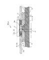
- the power supply device 104 used for the spacecraft includes the substrate 20, the chassis 10, the chassis-side resin portion 91, the fixing screw 29, and the insulating member 60.
- the board 20 has the electric component 25 mounted on the mounting surface 20b.
- the electric component 25 is covered with a metal package based on copper.
- the chassis 10 has a chassis surface 11 facing the back surface 20a of the mounting surface 20b, and a threaded portion 10a that has been subjected to threading. In FIG. 28, the threaded portion 10a is formed by excavating the surface of the chassis 10. A thread is cut inside the threaded portion 10a.
- the threaded portion 10a is formed integrally with the chassis 10.
- the chassis-side resin portion 91 is disposed between the rear surface 20a of the substrate 20 and the chassis surface 11, and is connected to the rear surface 20a and the chassis surface 11, and has an insulating property having a thermal conductivity of 1 W / mK or more and 10 W / mK or less. It is a cured resin.
- the fixing screw 29 has a head portion 29a and a threaded shaft portion 29b.
- the insulating member 60 has a through hole 61 in which the fixing screw 29 is disposed.
- the insulating member 60 is made of a material such as glass epoxy, PTFE (Poly Tetra Fluoro Ethylene), or Kapton.
- the configuration of the type B1 configuration shown in FIG. 31 is different from the configuration shown in FIG. 15 in that the board fixing screw 31 has a washer 31a.
- the other configuration is the same as the fixing method using the substrate fixing screw 31 shown in FIG.
- both the electric component 25 and the board 20 are fixed to the chassis 10 using the fixing screw 29 and the insulating member 60.
- the electric component 25 and the substrate 20 have a through hole 25d and a through hole 20d, respectively.
- the insulating member 60 has a first arrangement part 60a and a second arrangement part 60b.
- the through-hole 61 penetrates the first arrangement part 60a and the second arrangement part 60b.
- the first arrangement part 60a is arranged in a space 71 formed by arranging the through hole 25d of the electric component 25 followed by the through hole 20d of the substrate 20.
- the second arrangement portion 60b is arranged outside the through-hole 25d of the electric component 25 and contacts the peripheral edge 25e of the through-hole 25d of the electric component 25.
- a washer 72 is attached to the fixing screw 29.
- the fixing screw 29 is provided on both the electric component 25 and the board 20 by screwing an end portion 29 c of the shaft portion 29 b exposed from the through hole 61 of the insulating member 60 in the direction of the chassis 10 to the threaded portion 10 a of the chassis 10. Is fixed to the chassis 10.
- the fixing screw 29 is disposed in the through-hole 61 of the insulating member 60 so that the electric component 25 and the chassis 10 are not electrically in contact with each other.
- FIG. 32 shows a heavy component 77.
- the heavy component 77 there is a component such as a multilayer ceramic capacitor or a tantalum capacitor.
- the heavy part 77 is supported by the columnar part 10b, and vibration caused by the heavy part 77 is reduced.
- the columnar portion 10b can be formed by shaving the surface of the chassis 10.
- the power supply device 104-2 includes a columnar portion 10b and a coupling screw 10c.
- the columnar portion 10b stands upright from the chassis surface 11 in a columnar shape, is subjected to screw processing, and has an end surface in the direction in which the columnar portion stands up is connected to the back surface 20a of the substrate 20.
- the columnar portion 10b is internally threaded.
- the coupling screw 10c is provided with a washer 10d, and is screw-coupled to the columnar portion 10b.
- a through hole 20e is formed in the substrate 20 at a position connected to the columnar portion 10b.
- the coupling screw 10c fixes the substrate 20 to the columnar portion 10b by screwing with the columnar portion 10b through a through hole 20e formed at a position connected to the columnar portion 10b.
- the power supply device 104-3 having the configuration A2-B1 will be described with reference to FIGS.
- the configuration of type B1 has been described for the power supply device 104-1 and will not be described.
- the configuration of type A2 will be described with reference to FIG.
- the chassis 10 is not provided under the substrate 20, as a type A2, the end 29c of the shaft portion 29b of the fixing screw 29 exposed from the space 71 formed by the through hole 25d and the through hole 20d is replaced with a washer 74 and a nut 73. Stopped at.
- the fixing screw 29 is inserted into the space 71 formed by arranging the through hole 25 d of the electric component 25 and the through hole 20 d of the substrate 20, and the shaft portion 29 b is inserted into the space 71. End 29c is exposed.
- the fixing screw 29 fixes the electric component 25 and the substrate 20 to each other by screwing the exposed end portion 29c to the nut 73.
- the power supply device 104-4 shown in FIG. 25 has a configuration of A2-B2.
- Type A2 is as described for power supply device 104-3
- type B2 is as described for power supply device 104-2.
- the power supply device 104-5 shown in FIG. 26 has a configuration of A3-B1.
- the configuration of type A3 will be described with reference to FIG. 30 showing type A3.
- the type A3 has a columnar configuration in which the threaded portion 10a is the same as the columnar portion 10b as compared to the type A1 in FIG.
- the threaded portion 10a in FIG. 30 can be created by shaving the surface of the chassis 10 similarly to the columnar portion 10b.
- the power supply device 104-6 shown in FIG. 27 has a configuration of A3-B2.
- the configuration of the type A3 is as described in the description of the power supply device 104-5.
- the configuration of type B2 is as described in the description of the power supply device 104-2.
- the power supply device 104-7 shown in FIG. 33 is different from the power supply device 104-6 in that the columnar threaded portion 10a is a separate component from the chassis 10.
- the threaded portion 10a is fixed to the chassis 10 from the back of the chassis 10 by screws 75 and washers 76.
- the inner surface of the threaded portion 10a is threaded.
- the mounting structure of the threaded portion 10a on the substrate 20 side is the same as that of the power supply device 104-6.
- the power supply device 104-7 is a combination with the configuration of the type B2.
- the configuration in which the columnar threaded portion 10a is a separate component may be combined with the configuration of the type B1.
- the columnar portion 10b of type B2 is formed integrally with the chassis 10, the columnar portion 10b of type B2 may be a separate component from the chassis 10, like the threaded portion 10a of the power supply device 104-7.
- the power supply device 104 located in the spacecraft is exposed to radiation.
- the transmittance of radiation such as ⁇ -rays, ⁇ -rays, electron beams, and neutron beams can be reduced.
- the total amount of radiation received by the power supply device 104 in 15 years is preferably 5 Mrad or less, more preferably from the viewpoint of preventing malfunction and characteristic deterioration of the analog semiconductor, in order to prevent the deterioration of the chassis-side resin portion 91 and the second resin portion 96. 2 Mrad or less is good.
- the total amount of radiation received by the power supply device 104 for 15 years is set to be in a range of 0.1 Mrad or more and 1 Mrad or less from the viewpoint of preventing malfunction and characteristic deterioration. It is most preferable to do so.
- the chassis-side resin portion 91 has a Shore A hardness of 50 or less after curing, and has a Shore A hardness of 70 or less after irradiating a total radiation amount of 5 Mrad received for 15 years.
- the chassis-side resin portion 91 has a tendency to increase in hardness because unreacted active groups react by irradiation and polymerization proceeds. However, when an excessive amount of radiation exceeding 50 Mrad is irradiated, the organic group in the side chain is cleaved, crosslinking proceeds, the resin shrinks, and the hardness is significantly increased.
- the chassis-side resin portion 91 in 15 years is 5 Mrad or less, the peak intensity of the organic group in the side chain is not changed by the structural analysis by FT-IR analysis, and the cleavage of the organic group in the side chain does not occur. Has not been confirmed. For this reason, if the total amount of radiation received by the chassis-side resin portion 91 in 15 years is 5 Mrad or less, the chassis-side resin portion 91 can be suitably used without lowering the heat discharge performance.
- the upper limit of the total amount of radiation received for 15 years is one of 5 Mrad, 2 Mrad, and a value in the range of 0.1 Mrad to 1 Mrad.
- the chassis-side resin portion 91 has a Shore A hardness of 50 or less after curing, and a Shore A hardness of 70 or less after irradiation with radiation at a total radiation amount of 5 Mrad in 15 years.
- FIG. 34 is a diagram for explaining the shielding of the radiation dose.
- FIG. 34 is a diagram showing an example of an artificial satellite structure 230 disclosed in, for example, JP-A-2003-291898.
- an electronic device 208 is an electronic device mounted on an artificial satellite.
- the electronic device 208 corresponds to the electric component 25.
- the central cylinder 221 has a cylindrical shape disposed at the center of the satellite structure 230.
- the web panel 222 is mounted on the outside of the central cylinder 221 in the radial direction and parallel to the central axis of the central cylinder 221.
- the ceiling panel 223 is attached to the upper ends of the central cylinder 221 and the web panel 222 in a horizontal direction, and forms a ceiling of the box-shaped satellite structure 230.
- the base panel 224 is attached horizontally from below the central cylinder 221 to form a bottom plate of the box-shaped satellite structure 230.
- the outer surface panel 225 is attached to the web panel 222, the ceiling panel 223, and the base panel 224, and forms the outer surface of the satellite structure 230.
- the power supply device 104 and other electronic devices are arranged around the central cylinder 221. By using each of them as a shield against radiation, the radiation dose to which the power supply device 104 and other electronic devices are exposed is adjusted during the life of the satellite, which is a spacecraft. By using the chassis-side resin portion 91 in an adjusted environment, deterioration of the chassis-side resin portion 91 due to the influence of radiation during the life of the artificial satellite can be reduced.
- the power supply device 104 of the twelfth embodiment includes the chassis-side resin portion 91, the heat of the power supply device can be exhausted with a simple heat exhaust structure.
- the board and the electric component are fixed to the chassis with fixing screws via the insulating member 60. Therefore, it is possible to provide a space power supply device having vibration resistance while ensuring electrical non-contact between the chassis and the electric components.
- the power supply device 104-3 and the power supply device 104-4 fix the electric component 25 and the board 20 to each other by the nut 73, so that the power supply apparatus 104 having a space between the board 20 and the chassis 10 is used.
- the power supply device 104 of the twelfth embodiment restricts the upper limit of the total amount of radiation received in 15 years to one of 5 Mrad, 2 Mrad, and a value in the range of 0.1 Mrad to 1 Mrad. . This limits the total amount of radiation received for 15 years, so that problems due to radiation-induced deterioration of the chassis-side resin portion 91 can be prevented. Therefore, the heat exhaust effect by the chassis-side resin portion 91 can be maintained for 15 years.
Abstract
電源装置(104-1)は、電気部品(25)が実装された基板(20)と、シャシ面(11)とネジ加工部(10a)とを有するシャシ(10)と、裏面(20a)とシャシ面(11)とに接続するシャシ側樹脂部(91)と、固定ネジ(29)と、絶縁部材(60)とを備える。固定ネジ(29)は、絶縁部材(60)に形成されている貫通孔からシャシ(10)の方向へ露出した固定ネジ(29)の端部(29c)がシャシ(10)のネジ加工部(10a)とねじ結合することで電気部品(25)と基板(20)との両方をシャシ(10)に固定する。また固定ネジ(29)は、絶縁部材(60)の貫通孔に配置されることで電気部品(25)とシャシ(10)とを電気的に非接触にする。
Description
本発明は、ポリイミド基板、ガラエポ基板などの従来基板を使用しても高発熱部品を実装できる高排熱構造を有する宇宙用電源に関する。
電気部品は自身の発熱あるいは周囲温度によって性能及び寿命が左右される。特に真空中で使用される電気部品は、地上と異なり周囲に冷却するための空気がないため、空気を媒体とした熱伝達及び空気への熱放射ができない。このため、宇宙用電源では、基板からシャシへの排熱設計が重要である。
また、近年、人工衛星の大電力化に伴い、搭載される機器の消費電力も増加しており、排熱設計が重要な技術となっている。特に、スイッチング電源で使用するFET(Field Effect Transistor)及びダイオードは高発熱の電気部品である。従来は排熱対策として基板のシャシ固定用のネジに近い位置に高発熱の電気部品を実装している。あるいは、高発熱の電気部品をシャシに直接取り付けて、リード曲げの工夫、または基板への配線を伸張する工夫により、電気部品が基板上のパターンと電気的に接続されていた。
また、近年、人工衛星の大電力化に伴い、搭載される機器の消費電力も増加しており、排熱設計が重要な技術となっている。特に、スイッチング電源で使用するFET(Field Effect Transistor)及びダイオードは高発熱の電気部品である。従来は排熱対策として基板のシャシ固定用のネジに近い位置に高発熱の電気部品を実装している。あるいは、高発熱の電気部品をシャシに直接取り付けて、リード曲げの工夫、または基板への配線を伸張する工夫により、電気部品が基板上のパターンと電気的に接続されていた。
www.irf.com/technical-info/whitepaper/hermsmd.pdf「New Materials and Technologies Solve Hermetic SMD Integration」[平成28年12月27日検索]
しかし、上記の取り付け方法では、配線経路が長くなることによるインダクタンス成分の増加または損失、EMC(Electromagnetic Compatibility)の影響及び実装時に作業工程が増えるという課題があった。
更には、排熱を促すために基板とシャシとを接続しているネジの本数を増やすこと、発熱部品を極力ネジの近くに配置すること、または多数の部品を使用して分流することにより、発熱密度を抑制する対策が必要である。このため、電源の大型化及び質量増加を招くという課題があった。
また、人工衛星のような宇宙機で使用される電源装置は、振動対策及び放射線に照射されることの考慮が求められる。
また、人工衛星のような宇宙機で使用される電源装置は、振動対策及び放射線に照射されることの考慮が求められる。
この発明は、発熱部品の配線経路が長くならず、基板とシャシとを接続するネジの本数を増加させる必要のない、電源装置における簡易な構成の排熱構造の提供を目的とする。
また、この発明は、振動対策及び放射線対策が施された宇宙用電源装置の提供を目的とする。
また、この発明は、振動対策及び放射線対策が施された宇宙用電源装置の提供を目的とする。
この発明の電源装置は、
宇宙機に用いられる電源装置であって、
電気部品が実装面に実装された基板と、
前記実装面の裏面に対向するシャシ面と、ネジ加工が施されたネジ加工部とを有するシャシと、
前記基板の前記裏面と前記シャシ面との間に配置され、前記裏面と前記シャシ面とに接続する、熱伝導率が1W/mK以上10W/mK以下の絶縁性の樹脂硬化物であるシャシ側樹脂部と、
ネジ加工された軸部を有する固定ネジと、
前記固定ネジが配置される貫通孔が形成されている絶縁部材と、
を備え、
前記電気部品と前記基板とは、
貫通孔が形成されており、
前記絶縁部材は、
前記電気部品の前記貫通孔に前記基板の前記貫通孔が続いて配置されて形成された空間に配置された第1配置部と、
前記電気部品の前記貫通孔の外側に配置されて前記電気部品の前記貫通孔の周縁に当たる第2配置部と、
を有し、
前記固定ネジは、
前記絶縁部材の前記貫通孔から前記シャシの方向へ露出した前記軸部の端部が前記シャシの前記ネジ加工部とねじ結合することで前記電気部品と前記基板との両方を前記シャシに固定すると共に、前記絶縁部材の前記貫通孔に配置されることで前記電気部品と前記シャシとを電気的に非接触にする。
本発明はシャシ側樹脂部を備えたので、簡易な構成の排熱構造を有する電源装置を提供できる。
また本発明の電源装置では、基板と電気部品とが絶縁部材を介して、固定ネジでシャシに固定される。よって、シャシと電気部品との電気的な非接触を確保した上で、耐振動を有する宇宙用の電源装置を提供できる。
また本発明の電源装置では、基板と電気部品とが絶縁部材を介して、固定ネジでシャシに固定される。よって、シャシと電気部品との電気的な非接触を確保した上で、耐振動を有する宇宙用の電源装置を提供できる。
以下、本発明の実施の形態について、図を用いて説明する。なお、各図中、同一または相当する部分には、同一符号を付している。実施の形態の説明において、同一または相当する部分については、説明を適宜省略または簡略化する。実施の形態1から実施の形態8では構成の異なる宇宙用の電源装置100を説明する。宇宙用の電源装置100は、以下では電源装置100と記す。
電源装置100は、実施の形態1から実施の形態8のうちの一つの構成を有してもよいし、実施の形態1から実施の形態8のうちの複数の構成を有してもよい。
なお、以下の実施の形態では、例えば電源装置100-1のように「-1」をつけて電源装置100を区別する。
電源装置100は、実施の形態1から実施の形態8のうちの一つの構成を有してもよいし、実施の形態1から実施の形態8のうちの複数の構成を有してもよい。
なお、以下の実施の形態では、例えば電源装置100-1のように「-1」をつけて電源装置100を区別する。
実施の形態1.
***構成の説明***
図1から図3を参照して、実施の形態1の電源装置100-1を説明する。なお、電源装置100-1は地上において、真空あるいは真空に近い環境で使用されてもよい。
***構成の説明***
図1から図3を参照して、実施の形態1の電源装置100-1を説明する。なお、電源装置100-1は地上において、真空あるいは真空に近い環境で使用されてもよい。
図1は、電源装置100-1の断面図である。なお、電気部品25及びネジは断面を表していない。図1にはxyz座標系を示している。実施の形態2~9も同じ座標系を示す。実施の形態2から実施の形態9の断面図である図4、図6~図14は図1と同じ箇所の断面を示す。
電源装置100-1は、シャシ10と、電気部品25が実装されてシャシ10に固定される基板20と、基板20をシャシ10に固定する固定部30とを備える。電源装置100-1では固定部30は基板固定ネジ31である。
図2は、シャシ10の部分的な平面図(図1における-Z方向矢視)及びE-E断面を示す。E-E断面が図1,4,6-16,21に対応する。ネジ孔12には、基板固定ネジ31がねじ込まれる。図1ではシャシ10と基板20との一部を記載している。シャシ10ではネジ孔12は複数存在する。各ネジ孔12に基板固定ネジ31がねじ込まれる。基板固定ネジ31およびネジ孔12は、基板20の外周に沿った周縁部に複数配置され、例えば長方形の四隅または四辺に所定の間隔で設けられる。
図3は、図2の範囲13に相当する部分、つまり図1を-Z方向から見た矢視を、模式的に示す図である。
図2は、シャシ10の部分的な平面図(図1における-Z方向矢視)及びE-E断面を示す。E-E断面が図1,4,6-16,21に対応する。ネジ孔12には、基板固定ネジ31がねじ込まれる。図1ではシャシ10と基板20との一部を記載している。シャシ10ではネジ孔12は複数存在する。各ネジ孔12に基板固定ネジ31がねじ込まれる。基板固定ネジ31およびネジ孔12は、基板20の外周に沿った周縁部に複数配置され、例えば長方形の四隅または四辺に所定の間隔で設けられる。
図3は、図2の範囲13に相当する部分、つまり図1を-Z方向から見た矢視を、模式的に示す図である。
図1の電源装置100-1では、電気部品25が実装された基板20がシャシ10に固定されている。電気部品25の電極26は、基板20の一方の面20aの裏面の他方の面20bであるC面に接続している。基板20には後述する充填スルーホール21が形成されている。図1では10個の充填スルーホール21を示している。矢印で示している、電気部品25で発生した熱8は、充填スルーホール21から後述の絶縁樹脂硬化物27-1を経由してシャシ面11へ伝わる。
このように、電源装置100-1は、基板20と、シャシ10と、シャシ側樹脂部91である絶縁樹脂硬化物27-1とを備え、基板20には電気部品25が実装されている。シャシ10は、基板20の一方の面20aに対向する面であるシャシ面11を有する。絶縁樹脂硬化物27-1は、基板20の一方の面20aとシャシ面11との間に配置される。絶縁樹脂硬化物27-1は、一方の面20aとシャシ面11とに接続する、熱伝導率が1W/mK以上10W/mK以下の絶縁性の樹脂硬化物である。
(基板20)
基板20には発熱量の大きい電気部品25が取り付けられる。本実施の形態では、発熱量の大きい電気部品25として、SMD(Surface Mount Device)タイプのFETを使用する。通常、SMDタイプのFETで発生した熱は、FETの電極から基板20の回路パターンに伝わり、面内方向に伝わり、ネジ留め部を介してシャシ10に伝わる。
基板20には発熱量の大きい電気部品25が取り付けられる。本実施の形態では、発熱量の大きい電気部品25として、SMD(Surface Mount Device)タイプのFETを使用する。通常、SMDタイプのFETで発生した熱は、FETの電極から基板20の回路パターンに伝わり、面内方向に伝わり、ネジ留め部を介してシャシ10に伝わる。
(充填スルーホール)
電源装置100-1では、図1に示すように高熱伝導性の絶縁樹脂組成物(硬化前の絶縁樹脂硬化物27-1)で、基板20の一方の面20aであるS面と、シャシ10のシャシ面11との間をポッティング(モールド)する。これにより、絶縁樹脂組成物である高熱伝導性ポッティング樹脂を経路として、電気部品25の熱をシャシ10に伝える。このとき、基板20の厚さ方向(他方の面20bであるC面からS面)への熱伝導を向上させるために、基板20のC面からS面へ貫通するスルーホールが設けられている。スルーホールはメッキが施されている。メッキ後のスルーホールの内部には、はんだ、あるいはその他の金属、あるいは高熱伝導性を有するポッティング樹脂、が充填される。このスルーホールを充填スルーホール21と呼ぶ。
電源装置100-1では、図1に示すように高熱伝導性の絶縁樹脂組成物(硬化前の絶縁樹脂硬化物27-1)で、基板20の一方の面20aであるS面と、シャシ10のシャシ面11との間をポッティング(モールド)する。これにより、絶縁樹脂組成物である高熱伝導性ポッティング樹脂を経路として、電気部品25の熱をシャシ10に伝える。このとき、基板20の厚さ方向(他方の面20bであるC面からS面)への熱伝導を向上させるために、基板20のC面からS面へ貫通するスルーホールが設けられている。スルーホールはメッキが施されている。メッキ後のスルーホールの内部には、はんだ、あるいはその他の金属、あるいは高熱伝導性を有するポッティング樹脂、が充填される。このスルーホールを充填スルーホール21と呼ぶ。
このように、基板20は、一方の面20aから他方の面20bへ貫通するスルーホールに熱伝達材が充填された充填スルーホール21を備える。そして、絶縁樹脂硬化物27-1は、一方の面20aに現れた充填スルーホール21の一方の端部21aに接続している。なお充填スルーホール21に充填されている熱伝達材は、金属と、熱伝導率が1W/mK以上10W/mK以下の絶縁性の樹脂硬化物などである。
次に、絶縁樹脂硬化物27-1及び絶縁樹脂硬化物27-1のもとになる液状の絶縁樹脂組成物の特性を説明する。なお、詳細は以下で説明するが、絶縁樹脂硬化物27-1では、シリコーンあるいはウレタンがベース樹脂として用いられる。また絶縁樹脂硬化物27-1では、無機充填材として、アルミナ、窒化ホウ素、窒化アルミ、酸化マグネシウム、酸化ベリリウムのうち少なくとも一つを含有しており、絶縁樹脂硬化物27-1は硬度がショアAの硬度で70以下であり、300℃加熱時の低分子成分揮発量が1000ppm以下であり、ガラス転移点が-20℃以下である。
基板20のS面とシャシ10との間の高熱伝導性の絶縁樹脂硬化物27-1の形成方法としては、以下の(1)、(2)等の方法がある。
(1)シャシ10に基板20を固定した後、液状の絶縁樹脂組成物をシャシ10と基板20との間に流し込み、絶縁樹脂組成物を加熱硬化させて形成する方法がある。
(2)あるいは、シャシ10の底面に絶縁樹脂硬化物27-1を形成した後に、基板20を基板固定ネジ31でシャシ10に固定する。この(2)の方法の場合、絶縁樹脂硬化物27-1の硬度によるが、基板20をシャシ10へ取り付ける前における、絶縁樹脂硬化物27-1の厚みL2は、基板20のS面(一方の面20a)とシャシ10のシャシ面11との間の幅L1の110%以上250%以下の範囲の厚みになるように形成する。
つまり、
L2=(1.1~2.5)×L1
である。
さらに、より好ましくは、基板20をシャシ10へ取り付ける前における、
絶縁樹脂硬化物27-1の厚みL2は、幅L1の120%以上200%以下の範囲がよい。
つまり、
L2=(1.2~2.0)×L1
である。絶縁樹脂硬化物27-1の厚みL2をこの範囲内に形成する場合、基板20との固定部30により、S面と絶縁樹脂硬化物27-1との界面がより強固に密着し、排熱効果が高まる。さらに、使用環境時の冷熱サイクルによる厚み減少があった場合の排熱低下を抑制することができる。絶縁樹脂硬化物27-1の厚みが、S面とシャシ面11との間の幅の110%より薄い場合は、
つまり、
L2<1.1×L1
の場合、冷熱サイクルによる絶縁樹脂硬化物27-1の厚み減少により排熱効果が低下する。
また、厚みL2が厚みL1の200%を超える場合は、
つまり、
L2>2.0×L1
の場合、基板20をシャシ10にネジで固定する時に基板20が変形し、この変形が原因となって、冷熱サイクルで基板20に亀裂が入る恐れがある。
上記の(1)及び(2)の方法では、基板20のS面を上(+Z方向)に向けて、液状の絶縁樹脂組成物を流し込み、絶縁樹脂硬化物27-1を形成してもよい。この場合も、絶縁樹脂硬化物の厚みL2は、上記(2)で述べた厚みになるようにする。
次に、形成した絶縁樹脂硬化物27-1とシャシ10とが接するように基板20をネジでシャシ10に固定する。このようにすることで、S面上の配線パターンなどの高電圧部位に絶縁弱点部となる気泡が残らない。
次に、形成した絶縁樹脂硬化物27-1とシャシ10とが接するように基板20をネジでシャシ10に固定する。このようにすることで、S面上の配線パターンなどの高電圧部位に絶縁弱点部となる気泡が残らない。
(絶縁樹脂組成物及び硬度)
絶縁樹脂組成物は、液状の絶縁樹脂に、高熱伝導性を付与する無機充填材として、アルミナ、窒化ホウ素、窒化アルミ、酸化マグネシウム、酸化ベリリウムのうち少なくとも一つを含有した液状の絶縁樹脂組成物であるとする。
つまり、
<液状の絶縁樹脂組成物=[液状の絶縁樹脂+無機充填材]>+熱硬化→絶縁樹脂硬化物27-1である。液状の絶縁樹脂組成物が硬化して得られる絶縁樹脂硬化物27-1の硬度は、80以下(ショアA)であり、さらに好ましくは70以下である。
硬度が80を超える場合、基板20との接着性が低下して排熱効果が得られない恐れ及び基板20が変形する恐れがある。
硬度はショアA硬度計を代表として標記している。柔かい材料はショアEやショア00、ASKER Cなどで測定してもよい。ショアA80以下であれば、ショアEやショア00、ASKER Cで測定してもよい。
(硬化物の低分子成分含有量)
また、絶縁樹脂硬化物27-1を細かく切断し、ヘキサンやアセトンなどの有機溶媒で絶縁樹脂硬化物27-1の成分を抽出する。ガスクロマトグラフ質量分析装置(GC/MS)を使用し、その抽出溶媒を、ヘリウムをキャリアガスとして使用して、40℃から300℃まで昇温しながら、低分子成分量を分析する。その低分子成分量は、2000ppm以下、好ましくは1000ppm以下である。
2000ppmを超える場合は、絶縁樹脂硬化物27-1の使用時の冷熱サイクルで電気部品及び配線が汚染されたり、電気接点障害を引き起こしたり、電気部品特性が劣化する恐れがある。
(硬化物のアウトガス)
絶縁樹脂硬化物27-1を、ASTM E595に準拠し、真空環境下(7×10⁻³Pa 以下)において、加熱温度:125℃、保持時間:24時間、放出ガス冷却温度:25℃の試験条件で試験する。この試験条件で絶縁樹脂硬化物27-1から放出されるアウトガスを測定する。
測定結果から算出した質量損失比(TML:Total Mass Loss)は1%以下、再凝縮物質量比(CVCM:Collected Volatile Condensable Material)が0.1%以下であるべきある。
TMLが1%を超えたり、CVCMが0.1%を超える場合は、使用時の冷熱サイクルで電気部品及び配線が汚染されたり、電気接点障害を引き起こしたり、電気部品特性が劣化する恐れがある。
(ガラス転移点)
絶縁樹脂硬化物27-1のガラス転移点は、-10℃以下、好ましくは-20℃以下である。より好ましくは絶縁樹脂硬化物27-1の使用時の冷熱サイクル温度の低温側より低い温度が好ましい。ガラス転移点が-10℃より高い場合は、絶縁樹脂硬化物27-1の使用時の冷熱サイクルにおいて、絶縁樹脂硬化物27-1の変形が大きくなり安定な排熱が得られない恐れ、あるいは基板20の反りを引き起こすことなどの恐れがある。
絶縁樹脂硬化物27-1のガラス転移点は、-10℃以下、好ましくは-20℃以下である。より好ましくは絶縁樹脂硬化物27-1の使用時の冷熱サイクル温度の低温側より低い温度が好ましい。ガラス転移点が-10℃より高い場合は、絶縁樹脂硬化物27-1の使用時の冷熱サイクルにおいて、絶縁樹脂硬化物27-1の変形が大きくなり安定な排熱が得られない恐れ、あるいは基板20の反りを引き起こすことなどの恐れがある。
(液状の絶縁樹脂)
液状の絶縁樹脂としては、シリコーン樹脂あるいはウレタン樹脂の液状の熱硬化性樹脂とすることができる。
液状の絶縁樹脂としては、シリコーン樹脂あるいはウレタン樹脂の液状の熱硬化性樹脂とすることができる。
(シリコーン樹脂)
シリコーン樹脂は、室温で液状であれば公知のものを使用することができる。シリコーン樹脂は、硬化システムが付加反応型と縮合反応型とのいずれでも良い。シリコーン樹脂は、硬化後がゴム状(エラストマー)であっても、ゲル状であっても構わない。
例えば、ベースポリマーは平均分子量5,000~10万であり、25℃での粘度が1~100,000Pa・sの液状である。ベースポリマーは側鎖と末端にアルキル基、アルケニル基、アリル基、水酸基、水素基、アルコキシアルキル基、アルコキシシリル基の少なくとも1種類を有する直鎖状、環状、分岐状あるいは、梯子状の主鎖構造を有する公知のオルガノポリシロキサンである。ベースポリマーは、2種以上のオルガノポリシロキサンの混合物でも良い。
付加反応型の場合、ベースポリマーとして、アルケニル基を含むオルガノポリシロキサン、架橋剤として水素シロキサン、触媒として白金化合物を含有する組成を用いることができる。これらの配合量は、硬化反応が進行し、硬化後に必要な硬度が得られ、公知の有効量で良い。
縮合反応型の場合、ベースポリマーとして、シラノール基を含むオルガノポリシロキサン、架橋剤としてアルコキシシランやアセトキシシランなどのシラン化合物、触媒として有機錫化合物を含有する組成を用いることができる。
これらの配合量は、硬化反応が進行し、硬化後に必要な硬度が得られ、従来公知の有効量で良い。
(ウレタン樹脂)
ウレタン樹脂は、主剤として1分子中に複数の水酸基を持つポリオール樹脂と硬化剤としての1分子中に2個以上のイソシアネート基をもつ化合物を組み合わせ、共重合させることで得られる組成内にウレタン結合を有する樹脂である。
ウレタン樹脂は、混合後に25℃での粘度が1~100,000Pa・sの液状であれば、公知のものを使用できる。
例えば、ポリオール樹脂としては、公知のポリエステル系ポリオール、ジカルボン酸エステル系ポリオール、ポリエーテル系ポリオール、ポリテトラメチレンポリオキシグリコール、ひまし油系ポリオール、ε-カプロラクトン系ポリオール、ポリオキシポリアルキレン系ポリオール、β-メチル-δ-バレロラクトン系ポリオール、カーボネート系ポリオール等を用いてもよく、これらの2種以上を併用することもできる。
イソシアネート化合物としては、公知のトリレンジイソシアネート、ナフタレンジイソシアネート、ヘキサメチレンジイソシアネート、キシリデンジイソシアネート、ジフェニルメタンジイソシアネート、イソホロンジイソシアネート、シクロヘキシルジイソシアネート等を用いてもよく、これらの2種以上を併用することもできる。
また、ウレタン化反応を促進させるため、適宜のウレタン化触媒を用いることができる。このウレタン化触媒としては、第3級アミン化合物や有機金属化合物等の公知の触媒を用いることが可能である。ウレタン化触媒としては、例えば、トリエチレンジアミン,N,N’-ジメチルヘキサメチレンジアミン,N,N’-ジメチルブタンジアミン,ジアザビシクロ(5,4,0)ウンデセン―7(DBU)及びDBU塩、オクチル酸鉛,ラウリル酸ジブチル錫、ビスマストリス(2-エチルヘキサノエート)、ジイソプロポキシビス(エチルアセトアセテート)チタン、等が挙げられる。
ポリオールとイソシアネート化合物の配合に関しては、ポリオールの水酸基(OH)に対するイソシアネートのイソシアネート基(NCO)の当量比から算出する。当量比(NCO/OH)は、特に規定するものではないが、0.95~1.05の範囲とすることが好ましい。この当量比が1.05を超える場合は、絶縁樹脂組成物の硬化物の硬度が高くなり好ましくない。また、副生成物の炭酸ガスにより硬化物内にボイドが残存し、絶縁特性を低下させるために好ましくない。一方、この当量比が0.95未満の場合は、硬化の反応の進行が遅く、未硬化物となりやすく生産安定性に欠けるため好ましくない。また耐熱性に欠けるために好ましくない。
(熱伝導性を得る充填剤)
熱伝導性を有する充填材は、組成物(硬化物)に熱伝導性を付与する役割を有し、公知の熱伝導性の充填材を使用することができる。充填剤として、例えば、アルミナ粉末、酸化マグネシム粉末、窒化ホウ素粉末、窒化アルミニム粉末、酸化ベリリウム粉末、酸化亜鉛粉末、窒化珪素粉末、酸化ケイ素粉末、アルミニウム粉末、銅粉末、銀粉末、ニッケル粉末、金粉末、ダイヤモンド粉末、カーボン粉末、インジウム、及びガリウムなどが挙げられる。
熱伝導経路だけでなく、基板20とシャシ10との間に絶縁性を確保する必要がある場合は、アルミナ粉末、酸化マグネシム粉末、窒化ホウ素粉末、窒化アルミニム粉末、酸化ベリリウム粉末、酸化ケイ素粉末の高い絶縁性を有する粉末を使用することが好ましい。
このような熱伝導性充填材は、1種単独であるいは2種以上を混ぜ合わせて使用してもよい。熱伝導性充填材は、10W/m・K以上の熱伝導率を有するものが好ましい。熱伝導率が10W/m・Kより小さいと、組成物(硬化物)に十分な熱伝導率を付与できないためである。熱伝導性を付与するための充填材の平均粒径は、
0.1μm以上200μm以下、
好ましくは、
0.5μm以上100μm以下である。
このような平均粒径の熱伝導性充填材は、1種単独であるいは粒径が異なる2種以上を混ぜ合わせて使用してもよい。平均粒径が0.1μm未満の熱伝導性充填材は、粒子同士が凝集し易くなり流動性に乏しいものとなることがあるため好ましくない。平均粒径が100μm超過の熱伝導性充填材は、粒子が沈降しやすく、硬化物の熱伝導率が不均一になることがあるため好ましくない。
充填材の形状は、不定形でも球形でも如何なる形状でも構わない。なお、平均粒径は、レーザー光回折法による粒度分布測定における体積平均値D50(即ち、累積体積が50%になるときの粒子径又はメジアン径)として測定することができる。
(液状の絶縁樹脂組成物)
絶縁樹脂組成物は、上記の液状絶縁樹脂に、上記の高熱伝導性を付与するための無機充填材を混合して得られる。充填材の配合量が増加すると、硬化物の熱伝導率は上昇する。その場合、組成物の粘度は高くなり、作業性が低下し、あるいは硬化物の硬度が高くなることで基材との密着性が低下する。これらにより、目的とする排熱効果を得ることができない可能性もある。
従って、液状の絶縁樹脂組成物に含有される無機充填材の配合割合は、無機充填材が配合された絶縁樹脂組成物の25℃における粘度が、300Pa・s以下であれば特に限定されない。
さらに、絶縁樹脂組成物を狭い隙間に流し込む必要がある場合は、その粘度は50Pa・s以下が望ましい。例えば、無機充填材は、
40vol%以上80vol%以下、
の範囲内に含まれることが好ましく、
50vol%以上75vol%以下、
の範囲内に含まれることがより好ましい。
80vol%を超える場合は、絶縁樹脂組成物の粘度が高くなり作業性が悪くなり、あるいは硬化物の硬度が高くなり安定した排熱特性を得られないために好ましくない。一方、粘度が40vol%未満の場合は、樹脂の比率が高く、硬化物の熱伝導率の向上が見込めないため、好ましくない。また、絶縁樹脂組成物の反応性や基材との接着性を制御するための、アセチレン化合物、各種窒素化合物、有機りん化合物、オキシム化合物、及び有機クロロ化合物等の反応制御剤、あるいはシランカップリング剤などの密着性改質剤などの添加剤を必要に応じて、適宜加えても構わない。
(硬化条件)
液状の絶縁樹脂組成物の硬化条件は、公知のシリコーンポッティング材あるいはウレタンポッティング材と同様の条件とすることができる。
硬化温度は、
室温から180℃以下が良く、
より好ましくは
室温から150℃以下
である。
硬化温度が室温以下では、硬化が不十分で、使用時の冷熱サイクルで未反応原料が揮発し、電気部品を汚染する恐れがある。一方、硬化温度が150℃を超える場合は、電気部品の耐熱温度を超える恐れがあり、電気部品劣化を引き起こす可能性がある。
硬化時間は、所要の硬度が得られれば限定しないが、
室温の場合
48時間以下、好ましくは
24時間以下、
加熱硬化の場合は、
0.1時間以上12時間以下、
好ましくは
0.5時間以上6時間以下
である。
絶縁樹脂硬化物27-1の使用時のアウトガスの懸念がある場合は、加熱硬化することが好ましい。例えば、電気部品の使用許容の上限温度で加熱処理すれば、硬化物内部の揮発しやすい低分子成分を減少させ、アウトガスによる悪影響を回避することができる。
絶縁樹脂組成物の硬化物の絶縁破壊電界は、
10kV/mm以上が良く、より好ましくは15kV/mm以上である。
10kV/mm未満の場合は、使用電圧によっては、電気部品の配線間、基板20の配線パターン間の距離を長くする必要があり、電源部材の小型化の寄与が小さくなる。
(絶縁樹脂硬化物の体積抵抗率)
絶縁樹脂組成物の硬化物の体積抵抗率は、
1.0E+10Ω・cm以上が良く、より好ましくは
1.0E+12Ω・cm以上である。
1.0E+10Ω・cm未満の
場合は、使用電圧によっては、電気部品の配線間、基板20の配線パターン間の距離を長くする必要があり、電源部材の小型化の寄与が小さくなる。液状の絶縁樹脂組成物を発熱部品上あるいは基材上にポッティングしたり、筺体内に流し込んだりする前に、接着性を改善する表面改質剤(プライマー)で、これら被着体を処理しても構わない。公知のシリコーン用あるいはウレタン用プライマーを使用することができる。
絶縁樹脂組成物の硬化物の体積抵抗率は、
1.0E+10Ω・cm以上が良く、より好ましくは
1.0E+12Ω・cm以上である。
1.0E+10Ω・cm未満の
場合は、使用電圧によっては、電気部品の配線間、基板20の配線パターン間の距離を長くする必要があり、電源部材の小型化の寄与が小さくなる。液状の絶縁樹脂組成物を発熱部品上あるいは基材上にポッティングしたり、筺体内に流し込んだりする前に、接着性を改善する表面改質剤(プライマー)で、これら被着体を処理しても構わない。公知のシリコーン用あるいはウレタン用プライマーを使用することができる。
上記の電源装置100-1の製造方法の概要をまとめると、基板20とシャシ10との間に樹脂を流し込む製法は以下のようである。
電源装置100-1の製造方法は、
シャシ面11に対して、基板20の一方の面20aがシャシ面11に対向するように基板20を配置する基板配置工程と、
基板20の一方の面20aとシャシ面11との間に、絶縁性を有する液状の樹脂組成物を流し込む流し込み工程と、
流し込まれた液状の樹脂組成物を硬化させてシャシ側樹脂部91を生成する硬化工程とを備える。
ここで、液状の樹脂組成物は、シリコーンあるいはウレタンをベース樹脂として用い、無機充填材として、アルミナ、窒化ホウ素、窒化アルミ、酸化マグネシウム、酸化ベリリウムのうち少なくとも一つを含有する。
シャシ側樹脂部27-1の硬度は、ショアAの硬度で70以下であることが好ましい。シャシ側樹脂部27-1は、300℃加熱時の低分子成分揮発量が1000ppm以下であり、ガラス転移点が-20℃以下であることが好ましい。
また、樹脂を硬化させた後、基板20をシャシ10に取り付ける電源装置100-1の製造方法の概要は以下のようである。
電源装置100-1の製造方法は、
シャシ面11に、絶縁性を有する液状の樹脂組成物を流し込む流し込み工程と、
シャシ面11に流し込まれた液状の樹脂組成物を硬化させて、シャシ側樹脂部91を生成する硬化工程と、
基板20の一方の面20aが、シャシ面11に対向し、かつ、シャシ側樹脂部91に密着するように、基板20をシャシ10に取り付ける取り付け工程と
を備える。
ここで、液状の樹脂組成物は、
シリコーンあるいはウレタンをベース樹脂として用い、無機充填材として、アルミナ、窒化ホウ素、窒化アルミ、酸化マグネシウム、酸化ベリリウムのうち少なくとも一つを含有する。
シャシ側樹脂部27-1の硬度は、ショアAの硬度で70以下であることが好ましい。シャシ側樹脂部27-1は、300℃加熱時の低分子成分揮発量が1000ppm以下であり、ガラス転移点が-20℃以下であることが好ましい。
また、上記のいずれの製法においても、液状の樹脂組成物の25℃における粘度は、300Pa・s以下が好ましい。
実施の形態2.
図4、図5を参照して実施の形態2の電源装置100-2を説明する。
図4は、電源装置100-2の断面図である。図5は、図3に対応する図であり、図4の-Z方向矢視に相当する模式的な図である。
図4、図5を参照して実施の形態2の電源装置100-2を説明する。
図4は、電源装置100-2の断面図である。図5は、図3に対応する図であり、図4の-Z方向矢視に相当する模式的な図である。
電源装置100-2は電源装置100-1に対して、宇宙用パワーMOSFETとして、TO-254パッケージのような、電極26であるリードが形成されているタイプの電気部品25を使用する。電源装置100-2では、発熱部品である電気部品25はTO-254である。電源装置100-2は、電源装置100-1に対して、以下の(1)~(3)が異なる。他は電源装置100-1と同じである。
(1)電気部品25の直下に充填スルーホール21を設けて、基板20のS面に熱を伝える構成である。
(2)電気部品25の下面と基板20との間には、電気部品25の熱8を充填スルーホール21に効率的に伝えるため、熱伝導材23が配置されている。熱伝導材23は、例えば、はんだペーストあるいは銀ペーストである。
(3)電気部品25は、基板20に固定ネジ29で固定される。
(1)電気部品25の直下に充填スルーホール21を設けて、基板20のS面に熱を伝える構成である。
(2)電気部品25の下面と基板20との間には、電気部品25の熱8を充填スルーホール21に効率的に伝えるため、熱伝導材23が配置されている。熱伝導材23は、例えば、はんだペーストあるいは銀ペーストである。
(3)電気部品25は、基板20に固定ネジ29で固定される。
通常、宇宙用として使用される同タイプの電気部品25は、電気部品25内(パッケージ内)において、基板20もしくはシャシ10等と接触する面に近い位置に半導体を実装する排熱設計とされている。そのため、図4の構成にすることで、効率よくシャシ10へ排熱できる。上記(1)~(3)以外の、はんだ、あるいはその他金属あるいは熱伝導性樹脂によるスルーホールへの充填、基板20のS面とシャシ10との間に高熱伝導率の樹脂を流し込むことは、実施の形態1と同様である。
実施の形態3.
図6を参照して実施の形態3の電源装置100-3を説明する。
図6は、電源装置100-3を説明する図である。電源装置100-3は、電源装置100-1に対して基板固定ネジ31の頭を、高い熱伝導率の樹脂27-2によってポッティングした構成である。電源装置100-3の他の構成は、電源装置100-1と同じ構成である。
図6を参照して実施の形態3の電源装置100-3を説明する。
図6は、電源装置100-3を説明する図である。電源装置100-3は、電源装置100-1に対して基板固定ネジ31の頭を、高い熱伝導率の樹脂27-2によってポッティングした構成である。電源装置100-3の他の構成は、電源装置100-1と同じ構成である。
宇宙では電源装置100-3の周囲に熱伝導に影響を与えるほどの空気等の気体が存在しないため、基板20からの発熱は、シャシ10へ基板20を固定している基板固定ネジ31から排熱される。しかし、空気等の気体がないため、基板固定ネジ31によって押圧されることにより形成される基板20とシャシ10の接触面積からのみ排熱される。このため、発熱量の増加と共に、ネジ数を増加させる必要がある。高熱伝導率の樹脂27-2により基板固定ネジ31を含む基板20の端部とシャシ10とをポッティング材にて覆うことにより、排熱経路を増やすことが可能である。この場合の樹脂27-2として、絶縁樹脂硬化物27-1と同じ樹脂を使用することができる。なお図2の説明で述べたように、シャシ10には複数のネジ孔12があり、これらのネジ孔12に基板固定ネジ31がねじ込まれる場合には、それらの基板固定ネジ31の頭部も樹脂27-2で覆う構成でもよい。なお、基板固定ネジ31およびネジ孔12は、基板20の外周に沿った周縁部に複数配置され、例えば長方形の四隅または四辺に所定の間隔で設けられる。
実施の形態4.
図7及び図8は、実施の形態4の電源装置100-4を示す図である。図7及び図8の電源装置100-4は、電源装置100-1に対して、固定部30の構成が異なる他は、電源装置100-1と同じである。
図7及び図8は、実施の形態4の電源装置100-4を示す図である。図7及び図8の電源装置100-4は、電源装置100-1に対して、固定部30の構成が異なる他は、電源装置100-1と同じである。
図7に示す電源装置100-4は、基板20とシャシ10との間にバネ特性を持ったバネ固定具33を備える構成である。一般的に絶縁樹脂硬化物27-1の熱膨張率は数百ppmであり、金属の数ppmから数十ppmと比較して大きい。そのため、シャシ10と基板20との間に充填した絶縁樹脂硬化物27-1が熱によって、厚み及び幅等の寸法が変化する際に、バネ固定具33により基板20も絶縁樹脂硬化物27-1の変化に追従することが可能となる。従って、基板20と絶縁樹脂硬化物27-1との剥離を抑制できる。図7では基板20とバネ固定具33とは、はんだ32aで接続されているが、図8の電源装置100-4のように、ネジ32bで締結してもよい。なお、基板固定ネジ31およびバネ固定具33は、基板20の外周に沿った周縁部に複数配置され、例えば長方形の四隅または四辺に所定の間隔で設けられる。
実施の形態5.
図9は、実施の形態5の電源装置100-5を示す図である。電源装置100-5は、電源装置100-1に対して、以下の(1)~(3)が異なる。他は電源装置100-1と同じである。
(1)電気部品25の電極26が、電気部品25の上にある。
(2)電極26と充填スルーホール21とが、電極接続部28-1である、ワイヤーあるいはブスバーで接続されている。
(3)電気部品25が基板20に接着剤24で固定されている。
図9は、実施の形態5の電源装置100-5を示す図である。電源装置100-5は、電源装置100-1に対して、以下の(1)~(3)が異なる。他は電源装置100-1と同じである。
(1)電気部品25の電極26が、電気部品25の上にある。
(2)電極26と充填スルーホール21とが、電極接続部28-1である、ワイヤーあるいはブスバーで接続されている。
(3)電気部品25が基板20に接着剤24で固定されている。
一般的に、基板20に実装される電気部品25では、電極26は基板20上の回路パターンに直接接続される。しかし、基板20と電気部品25との熱膨張率が大きく異なる場合は、熱サイクルにて、はんだ付け部にクラックが入ってしまう。このため、敢えて基板20とは逆の上方向に電気部品25の電極26を向け、上に向けた電極26に、ワイヤあるいはブスバーを電極延長部として接続して、ワイヤあるいはブスバーを基板20の回路パターンに接続する方法が取られる。このような場合において、ワイヤあるいはブスバーを、充填スルーホール21と接続し、排熱することが可能である。
排熱のため、図9では、電極26と充填スルーホール21とを接続する熱伝達材である電極接続部28-1として、ワイヤあるいはブスバーが使用される。
実施の形態6.
図10は、実施の形態6の電源装置100-6を示す図である。電源装置100-6は、電源装置100-5に対して、さらに、電気部品25と、ブスバーあるいはワイヤである電極接続部28-1とを、樹脂硬化物27-3で包み込んだ構成である。この構成により、熱伝導率を向上させることが可能となる。樹脂硬化物27-3は部品側樹脂部92である。
図10は、実施の形態6の電源装置100-6を示す図である。電源装置100-6は、電源装置100-5に対して、さらに、電気部品25と、ブスバーあるいはワイヤである電極接続部28-1とを、樹脂硬化物27-3で包み込んだ構成である。この構成により、熱伝導率を向上させることが可能となる。樹脂硬化物27-3は部品側樹脂部92である。
図10のように、充填スルーホール21は、基板20において電気部品25の周囲のいずれかの位置に配置されている。樹脂硬化物27-3は、シャシ側樹脂部91である絶縁樹脂硬化物27-1とともに基板20を間に挟むように、基板20に対して絶縁樹脂硬化物27-1の反対の位置に配置されている。樹脂硬化物27-3は、電気部品25と、基板20の他方の面20bに現れた充填スルーホール21の他方の端部21bと、電極接続部28-1とを封じ込める絶縁性の樹脂硬化物である。樹脂硬化物27-3として、絶縁樹脂硬化物27-1と同じ樹脂を使用することができる。
実施の形態7.
図11及び図12は実施の形態7の電源装置100-7を示す図である。図11に示す電源装置100-7は、電源装置100-6に対して、シャシ接続部28-2である排熱用のブスバーを、電気部品25の上部に設けた構成である。シャシ接続部28-2はネジ42でシャシ10に固定される。排熱用のブスバーにより、排熱を増加できる。この場合、図11の樹脂硬化物27-3は、絶縁性の樹脂硬化物である接触樹脂部93である。
図11及び図12は実施の形態7の電源装置100-7を示す図である。図11に示す電源装置100-7は、電源装置100-6に対して、シャシ接続部28-2である排熱用のブスバーを、電気部品25の上部に設けた構成である。シャシ接続部28-2はネジ42でシャシ10に固定される。排熱用のブスバーにより、排熱を増加できる。この場合、図11の樹脂硬化物27-3は、絶縁性の樹脂硬化物である接触樹脂部93である。
図12は、電気部品25の上部に接触樹脂部93である樹脂硬化物27-4を配置する構成である。なお、図12の電気部品25は、後述する図13に示す電気部品25と同様の電極26を有するが、電極26の並ぶ方向が図12ではY方向であり図13ではX方向である。樹脂硬化物27-4として、絶縁樹脂硬化物27-1と同じ樹脂を使用することができる。図12の構成により、SMDタイプのトランスあるいはICなど、基板20とは逆側である上部が樹脂硬化物27-4でモールドされた電気部品25の上部からも、排熱できる。
図11、図12に示すように、接触樹脂部93とシャシ側樹脂部91である絶縁樹脂硬化物27-1とが、基板20を間に挟む。
接触樹脂部93は基板20に対して絶縁樹脂硬化物27-1の反対の位置に配置されて、電気部品25の少なくとも一部と接触する。熱伝達性を有するシャシ接続部28-2は、接触樹脂部93とシャシ10とを接続する。
接触樹脂部93は基板20に対して絶縁樹脂硬化物27-1の反対の位置に配置されて、電気部品25の少なくとも一部と接触する。熱伝達性を有するシャシ接続部28-2は、接触樹脂部93とシャシ10とを接続する。
実施の形態8.
図13は、実施の形態8の電源装置100-8を示す図である。電源装置100-7では、排熱用として設けたブスバーであるシャシ接続部28-2をシャシ10に接続している。
電源装置100-8では、スルーホール接続部28-3が、基板20上の充填スルーホール21の他方の端部21bに接続している。これにより、熱8が絶縁樹脂硬化物27-1を介してシャシ10に排熱する。このため、図12の電源装置100-7よりも排熱経路を短くできる。
図13は、実施の形態8の電源装置100-8を示す図である。電源装置100-7では、排熱用として設けたブスバーであるシャシ接続部28-2をシャシ10に接続している。
電源装置100-8では、スルーホール接続部28-3が、基板20上の充填スルーホール21の他方の端部21bに接続している。これにより、熱8が絶縁樹脂硬化物27-1を介してシャシ10に排熱する。このため、図12の電源装置100-7よりも排熱経路を短くできる。
つまり図13に示すように、充填スルーホール21は、基板20において電気部品25の周囲のいずれかの位置に配置されている。接触樹脂部93とシャシ側樹脂部91である絶縁樹脂硬化物27-1とが基板20を間に挟む。接触樹脂部93は基板20に対して絶縁樹脂硬化物27-1の反対の位置に配置されて、電気部品25の少なくとも一部と接触する。スルーホール接続部28-3は、接触樹脂部93と、充填スルーホール21の他方の端部21bとを接続する。
実施の形態9.
図14は、実施の形態9を表す図である。実施の形態9は、電源装置100を大気が存在する環境で製造する方法に関する。実施の形態9は、真空ではなく、地上の通常の大気環境で基板20とシャシ10との間に絶縁樹脂硬化物27-1(絶縁樹脂組成物)の層を成形する作業、つまり、液状の絶縁樹脂組成物を注入する作業を示している。
実施の形態9では電源装置100-8を例としているが、実施の形態9の方法は、電源装置100-1から100-7にも適用できる。
図14は、実施の形態9を表す図である。実施の形態9は、電源装置100を大気が存在する環境で製造する方法に関する。実施の形態9は、真空ではなく、地上の通常の大気環境で基板20とシャシ10との間に絶縁樹脂硬化物27-1(絶縁樹脂組成物)の層を成形する作業、つまり、液状の絶縁樹脂組成物を注入する作業を示している。
実施の形態9では電源装置100-8を例としているが、実施の形態9の方法は、電源装置100-1から100-7にも適用できる。
図14の(a)は大気環境での好ましい製造方法を示し、図14の(b)は、大気環境での好ましくない製造方法を示している。図14の(a),(b)では、空気の流れを矢印44で示した。図14の(a)では液状の絶縁樹脂組成物と、気泡つまり空気との比重の差により、気泡は液状の絶縁樹脂組成物から上方であるZ方向へ向かうので大気中へと出ていくことになる。このため、空気を巻き込む確率が小さくなる。一方、図14の(b)の場合は、上方つまりZ方向へ向かう空気は基板20のS面で遮られてしまいボイド41が形成されやすい。図14の(a)の製造方法を用いることにより、大気中に於いても通常、基板20のS面に形成されやすく、熱伝導度を低下させる要因となるボイド41の形成を極力避けることが可能である。これにより、機器を真空容器に入れることなく樹脂層を成形でき、作業性が大幅に向上する。また、機器導入に関わるコストも削減可能である。
実施の形態1~9で述べた電源装置100は、高発熱部品が実装された基板のS面と、人工衛星の構体と接続されている電源のシャシとの間を宇宙環境に耐えうる高熱伝導率を有する液状絶縁樹脂にてポッティング(充填、モールド)し、及び基板とシャシを接続するネジ部を宇宙環境に耐えうる高熱伝導率を有する液状絶縁樹脂にてポッティング(充填、モールド)することにより、排熱パスを確保する。
すなわち、回路パターンとなる基板中の銅箔に依存する従来の熱伝導経路(基板面内方向)に加え、上記の排熱経路を設けて、電源の筐体であるシャシへの排熱能力を増加させることで、基板上の部品温度上昇を抑制することを可能とするものである。
すなわち、回路パターンとなる基板中の銅箔に依存する従来の熱伝導経路(基板面内方向)に加え、上記の排熱経路を設けて、電源の筐体であるシャシへの排熱能力を増加させることで、基板上の部品温度上昇を抑制することを可能とするものである。
***実施の形態の効果の説明***
高発熱部品の周囲または、その部品が実装されている基板とシャシの間を、宇宙環境に耐えうる高熱伝導率を有する液状絶縁樹脂にてポッティング(充填、モールド)することにより排熱パスを確保する。通常数十um~数百umの銅箔で構成される回路パターンから成る従来の熱伝導経路(基板面内方向)に加え、その基板とシャシとを高熱伝導率の樹脂にて接続し排熱経路を設ける。この排熱経路によって、基板の面外方向となるシャシ方向への排熱能力を増加させる。これにより基板上の部品温度上昇を抑制することが可能となる。
上記の高熱伝導率を有する液状絶縁樹脂は、高熱伝導性を付与する無機充填材として、アルミナ、窒化ホウ素、窒化アルミ、酸化マグネシウム、酸化ベリリウムのうち少なくとも一つを含有する。
液状絶縁樹脂の硬化物の硬度は70以下(ショアA)である。
また、液状絶縁樹脂の硬化物は、300℃加熱時の低分子成分揮発量が500ppm以下であり、ガラス転移点が-20℃以下である。上記で述べたように、液状絶縁樹脂の硬化物は、シリコーンあるいはウレタンがベース樹脂である。
この構成により、熱伝導性ポッティング樹脂で放熱路を確保することで、FET素子等の電気部品の温度上昇を抑制することが可能となり、電源の小型化または高出力化が可能である。ポリイミド基板、ガラエポ基板などの従来基板を使用しても高発熱部品を実装できる高排熱構造を提供することができる。
実施の形態10.
図15から図20を参照して実施の形態10を説明する。実施の形態10では、電源装置101-1,101-2、102-1、102-2,102-3、102-4を説明する。実施の形態10は、電気部品25のグランド端子25aの電位と、シャシ10の電位とを異なる電位に保持し、かつ、電気部品25の熱をシャシ10に伝達する電源装置に関する。実施の形態10の電源装置では、シャシ10が起立部を有する。
図15から図20を参照して実施の形態10を説明する。実施の形態10では、電源装置101-1,101-2、102-1、102-2,102-3、102-4を説明する。実施の形態10は、電気部品25のグランド端子25aの電位と、シャシ10の電位とを異なる電位に保持し、かつ、電気部品25の熱をシャシ10に伝達する電源装置に関する。実施の形態10の電源装置では、シャシ10が起立部を有する。
図15は、電源装置101-1の平面図及び断面図を示している。図15の上側の図は、電源装置101-1のZ1方向の平面図を模式的に示す。図15の上側の図では、充填スルーホール21は実線で示している。図15を参照して実施の形態10の電源装置101-1を説明する。
電源装置101-1は、シャシ10、基板20及びシャシ側樹脂部91を備えている。
基板20の一方の面20a及び他方の面20bは、以下、面20a及び面20bと記す。
基板20には電気部品25が実装されている。シャシ10は、基板20の面20aに対向する面であるシャシ面11と、シャシ面11から面20aに向かって起立すると共に起立方向15の端部14aが面20aと接触せずに、面20aに対向する起立部14を有する。起立部14は伝熱部94である。電気部品25に発生した熱が、起立部14に伝達される。シャシ側樹脂部91は、基板20の面20aと起立部14の端部14aとの間に配置され、面20aと端部14aとに接続している。シャシ側樹脂部91は、熱伝導率が1W/mK以上10W/mK以下の絶縁性の樹脂硬化物である。
図15に示すように、基板20は、面20aから面20bへ貫通するスルーホールに熱伝達材が充填された充填スルーホール21を備えている。シャシ側樹脂部91は、面20aに現れた充填スルーホール21の一方の端部21aと起立部14の端部14aとに接続している。充填スルーホール21の熱伝達材は、金属と、熱伝導率が1W/mK以上10W/mK以下の絶縁性の樹脂硬化物とのいずれかである。
図15において、シャシ10は、取り付け部16と、伝熱部94である起立部14とを有する。電気部品25のグランド端子25aは、固定ネジ29によって、電気部品25と共に取り付け部16に固定される。グランド端子25aは充填スルーホール21に、熱的に接続している。シャシ10は、絶縁体17を有し、電気部品25は、絶縁体17に固定ネジ29で固定されている。具体的には、固定ネジ29は、シャシ10に埋め込まれている絶縁体17に形成された雌ネジ18に係合する。図15に示すように、充填スルーホール21は、固定ネジ29とは接触していない。
起立部14は、端部14aの端面14bがシャシ面11から突出し、端面14bが基板20の面20aに近接している。シャシ側樹脂部91が、起立部14の端面14bと基板20の面20aとの間に充填されている。シャシ側樹脂部91は、電気部品25に熱的に接続している充填スルーホール21に、熱的に接続している。
充填スルーホール21の周囲は、基板20の非導電領域20cに囲まれている。非導電領域20cとは、基板20において導電性のない領域である。図15に示すように、非導電領域20cの沿面距離d1は、グランド端子25aから、定められた距離d以上の長さである。具体的には、グランド端子25aの端と起立部14の側面14cとの、面20aに沿う沿面距離d1は、定められた距離d以上の長さである。沿面距離d1が定められた距離d以上であることによって、高電圧の電気部品25を基板20に取り付けることが可能になる。電気部品25の電極26及びグランド端子25aの電位は、シャシ10とは異なる電位となる。
図15に示す電源装置101-1は、起立部14によって段差を設けたシャシ10と、基板20に設けた充填スルーホール21とを、シャシ側樹脂部91で埋めている構成である。この構成により、充填スルーホール21が、「段差の壁面である起立部14の側面14dおよび起立部14の端面14b」と、接続されているという特徴を持つ。
電気部品25の熱8は、基板20の充填スルーホール21からシャシ側樹脂部91に伝達し、シャシ側樹脂部91からシャシ10の起立部14に伝わる。また、電気部品25の熱8は、固定ネジ29の周囲から基板20を介して取り付け部16に伝達する。
電源装置では、基板20に形成されたスルーホールとシャシ10とを樹脂で接続し、一定方向に排熱させる構成の場合、排熱性能は樹脂の熱伝導率に大きく依存する。
これに対し、実施の形態10の電源装置では、シャシ10に、起立部14によって凸状の段差を設けている。また、後述する実施の形態11では、シャシ10に凹状の凹部55を設けている。
樹脂内の熱拡散により、凸状または凹状の壁面に熱を拡散させることによって、排熱パスが増え、または、樹脂の中で最短ルートの排熱パスが形成されてる。このような排熱パスによって排熱性能が向上するため、電源装置に、より高い排熱性を持たせることができる。
これに対し、実施の形態10の電源装置では、シャシ10に、起立部14によって凸状の段差を設けている。また、後述する実施の形態11では、シャシ10に凹状の凹部55を設けている。
樹脂内の熱拡散により、凸状または凹状の壁面に熱を拡散させることによって、排熱パスが増え、または、樹脂の中で最短ルートの排熱パスが形成されてる。このような排熱パスによって排熱性能が向上するため、電源装置に、より高い排熱性を持たせることができる。
図16は、電源装置101-1の変形例である電源装置101-2を示す。電源装置101-2は、電気部品25が部品側樹脂部92に覆われている。この点が電源装置101-1と異なるのみである。このように、電気部品25が部品側樹脂部92に覆われる構成でもよい。
図17は、電源装置102-1の平面図及び断面図を示している。
図17の上側の図は、電源装置102-1のZ1方向の平面図を模式的に示す。図17の上側の図では、起立部14-1の端面14bと、複数の充填スルーホール21との位置を示している。なお上側の図では、充填スルーホール21は実線で示している。
図17の上側の図は、電源装置102-1のZ1方向の平面図を模式的に示す。図17の上側の図では、起立部14-1の端面14bと、複数の充填スルーホール21との位置を示している。なお上側の図では、充填スルーホール21は実線で示している。
基板20は、面20aから面20bへ貫通するスルーホールに熱伝達材が充填された充填スルーホール21を備えている。起立部14-1は、シャシ側樹脂部91の内部でシャシ面11から面20aに向かって起立しており、起立方向15の端部14aが面20aに対向している。シャシ側樹脂部91は、面20aに現れた充填スルーホール21の一方の端部21aに接続している。
図17では、起立部14-1の端面14bは、基板20の面20aの非導電領域20cに当接している。つまり、起立部14-1の端部14aの端面14bは、非導電領域20cに接触している。面20aにおいて充填スルーホール21の一方の端部21aが現れていない領域は非導電領域20cである。
図17では、起立部14-1の端面14bは、基板20の面20aの非導電領域20cに当接している。つまり、起立部14-1の端部14aの端面14bは、非導電領域20cに接触している。面20aにおいて充填スルーホール21の一方の端部21aが現れていない領域は非導電領域20cである。
起立部14-1は、例えば柱形状である。起立部14-1は、例示すれば、円柱形状、三角柱形状、四角柱形状または5角以上の多角柱形状である。
図17では、非導電領域20cの回りには、複数の充填スルーホール21が配置される。図17の上側の図のように、非導電領域20cは、複数の充填スルーホール21に周囲を囲まれている。
図17に示すように、複数の充填スルーホール21の上に、電気部品25が配置されている。また起立部14は、シャシ側樹脂部91に囲まれている。なお、図17では、起立部14の端面14bは基板20の面20aと接触しているが、端面14bと基板20の面20aとの間に、シャシ側樹脂部91が充填されても良い。
図17に示すように、起立部14の端面14bの端部と、最も近い充填スルーホール21との、面20aに沿う沿面距離d1は、電源装置101-1と同様に、定められた距離d以上の長さである。これは電源装置102-2、102-3,102-4も同様である。
図18は、電源装置102-2の断面図である。
図19は、電源装置102-3の断面図である。
図20は、電源装置102-4の断面図である。
電源装置102-2、電源装置102-3及び電源装置102-4は、電源装置102-1に対して、起立部の形状が異なる。電源装置102-2の起立部14-2及び電源装置102-4の起立部14-4は、いずれも、起立方向15を法線の方向とする断面の形状が、起立方向15に向かって変化している。起立部14-2及び起立部14-4では、断面の形状が起立方向15に向かって次第に小さくなる。
図19は、電源装置102-3の断面図である。
図20は、電源装置102-4の断面図である。
電源装置102-2、電源装置102-3及び電源装置102-4は、電源装置102-1に対して、起立部の形状が異なる。電源装置102-2の起立部14-2及び電源装置102-4の起立部14-4は、いずれも、起立方向15を法線の方向とする断面の形状が、起立方向15に向かって変化している。起立部14-2及び起立部14-4では、断面の形状が起立方向15に向かって次第に小さくなる。
電源装置102-2の起立部14-2は、横断面積(外径)が変化している。電源装置102-2の起立部14-2は、シャシ面11から基板20の面20aに向かって、段階的に横断面積が小さくなる。電源装置102-2の起立部14-2は、外径の異なる複数の円柱を、シャシ面11ら基板20の面20aに向かって、外径の大きい順に積み上げた形状である。
電源装置102-3の起立部14-3は、シャシ面11から面20aに向かって、横断面積の外径が長径と短径を繰り返して変化する。
例えば、起立部14-3は螺旋形状もしくは縦断面が楔型状となっており、外周が凹凸形状をなす。
例えば、起立部14-3は螺旋形状もしくは縦断面が楔型状となっており、外周が凹凸形状をなす。
電源装置102-4の起立部14-4は、シャシ面11から基板20の面20aに向かって緩やかに、もしくは連続的に断面積が小さくなる。例えば起立部14-4は、円錐台形状もしくは多角錐台形状をなす。
***実施の形態10の効果の説明***
電源装置101-1及び電源装置101-2では、起立部14の端面14bと面20aとをシャシ側樹脂部91が接続している。また、沿面距離d1が、定められた距離d以上の長さである。よって、電源装置101-1及び電源装置101-2によれば、グランド端子25aの電位と、シャシ10の電位とを異なる電位に保持し、かつ、電気部品25の熱をシャシ10に伝達することができる。
電源装置101-1及び電源装置101-2では、起立部14の端面14bと面20aとをシャシ側樹脂部91が接続している。また、沿面距離d1が、定められた距離d以上の長さである。よって、電源装置101-1及び電源装置101-2によれば、グランド端子25aの電位と、シャシ10の電位とを異なる電位に保持し、かつ、電気部品25の熱をシャシ10に伝達することができる。
電源装置102-1から電源装置102-4では、起立部14の端面14bが面20aに接触している。起立部の端面14bと面20aとをシャシ側樹脂部91が接続している。さらに、沿面距離d1が、定められた距離d以上の長さである。よって、電源装置102-1から電源装置102-4によれば、グランド端子25aの電位と、シャシ10の電位とを異なる電位に保持し、かつ、電気部品25の熱をシャシ10に伝達することができる。
実施の形態11.
図21は、実施の形態11による電源装置103を示す図である。電源装置103では、シャシ面11に対して段差が設けられており、凹状の凹部55が存在する。凹部55は、図21では、角部AからDで示される。凹部55はシャシ面11よりも低い、底面11aを有する。
電源装置103は、電気部品25、基板20、基板20の面20aに対向するシャシ面11を有するシャシ10及びシャシ側樹脂部91を備える。基板20は、面20aの裏面である面20bのうち電気部品25で覆われる領域に、はんだレベラー54が形成されたはんだレベラー形成領域51を有し、面20aに、はんだレベラー54が形成されたはんだレベラー形成領域51を有する。また、基板20は、面20aから面20bへ貫通し、内面にはんだレベラー54が形成され電気部品25で覆われる領域に配置された複数のスルーホール52を有する。
シャシ側樹脂部91は、電気部品25と基板20の面20bに形成されたはんだレベラー形成領域51との間と、基板20の面20aに形成されたはんだレベラー形成領域51とシャシ10との間と、スルーホール52の内部とに配置される。
シャシ側樹脂部91は、熱伝導率が1W/mK以上10W/mK以下であり、硬度がショアA硬度計で70以下である。シャシ側樹脂部91は、絶縁性の樹脂硬化物である。
図21に示すように、スルーホール52に形成されたはんだレベラー52aは、面20aに形成されたはんだレベラー形成領域51と、面20bに形成されたはんだレベラー形成領域51とに接続している。
図21に示すように、電源装置103の特徴は、上記で述べたように、以下の(1)(2)(3)で説明している箇所に、樹脂硬化物であるシャシ側樹脂部91が配置されていることである。ここでシャシ側樹脂部91については、熱伝導率が1W/mK以上10W/mK以下であり、硬度がショアA硬度計で70以下である。シャシ側樹脂部91は、絶縁性の樹脂硬化物である。
(1)シャシ側樹脂部91は、電気部品25と、基板20の面20bに形成されているはんだレベラー形成領域51との間に配置されている。
はんだレベラー形成領域51では、基板20の面20bに施された銅メッキ53の表面に、はんだレベラー54が形成されている。
(2)シャシ側樹脂部91は、基板20の面20aに形成されているはんだレベラー形成領域51と、シャシ10との間に配置されている。
(3)シャシ側樹脂部91は、電気部品25の直下の基板20の領域に形成されたスルーホール52の内部に配置されている。
ここで、スルーホール52の内面には銅メッキ53が施されており、銅メッキ53の表面にはんだレベラー54が施されている。
スルーホール52の内部は、銅メッキ53とはんだレベラー54との積層構造である。
電源装置103では、発熱する電気部品25からシャシ10に至る排熱経路が、樹脂であるシャシ側樹脂部91で形成される。
硬度が低い樹脂を用いることで、熱衝撃及び振動で発生する応力が樹脂によって吸収または緩和できる。
このため、電気部品25、基板20、スルーホール52、シャシ10のそれぞれと、シャシ側樹脂部91の樹脂界面との剥離を抑制できるので、排熱信頼性を高めることができる。
電気部品25と基板20との間に低硬度のシャシ側樹脂部91を介在させることで、電気部品25と基板20との密着力が高まり、界面熱抵抗を低減できる。
電気部品25と基板20との間に設ける樹脂硬化物であるシャシ側樹脂部91の厚みは、熱抵抗を下げるために薄い方がよく、シャシ側樹脂部91の厚みは、0.25mm以下が好ましい。
尚、電気部品25は、樹脂モールド品、セラミックパッケージ品または金属ケースで覆われた構成のどれでも良い。
<変形例1>
また、図21に示すシャシ側樹脂部91として、粘度10Pa・s以上300Pa・s以下の液状樹脂組成物を用いても良い。
また、図21に示すシャシ側樹脂部91として、粘度10Pa・s以上300Pa・s以下の液状樹脂組成物を用いても良い。
10Pa・s以上の高粘度の液状樹脂組成物を、シャシ10の底面11aまたは基板20の面20bに、通常の場合よりもより厚く塗布する。
塗布された高粘度の液状樹脂組成物は、基板20を基板固定ネジ31でシャシ10に固定するとき、または、電気部品25が固定ネジ29で基板20に固定されるときに発生する圧力によって、スルーホール52の内部に充填される。
なお、10Pa・s以上の高粘度の液状樹脂組成物の粘度は、上記のように10Pa・s以上300Pa・s以下である。
ただし、液状樹脂組成物の粘度が高いほどネジ固定がしにくくなるため、より好ましくは、液状樹脂組成物の粘度は、50Pa・s~150Pa・sである。
粘度が10Pa・s以上の樹脂であっても、塗布時には、樹脂はスルーホール52に充填される。
しかし、硬化時に粘度が下がり、スルーホール52から流れ出る場合がある。その場合は、加熱硬化の可能な樹脂であれば、低温で樹脂を加熱して半硬化させた後、半硬化させた温度よりも高い硬化温度で樹脂を硬化させる。
これにより、スルーホール52からの流れ出しが、改善できる。
液状樹脂組成物の粘度が10Pa・s未満の場合、樹脂の硬化時に粘度が下がり、スルーホール52の内部に樹脂が留まらず、未充填領域が発生するおそれがあり、また、樹脂の硬化後に、スルーホール52の内部にボイドが残存するそれがある。これらの場合、樹脂が流動しないように、樹脂を堰きとめるための壁を設ける必要がある。
<変形例2>
また、樹脂硬化物が、同一樹脂で形成されてもよい。「同一樹脂」における同一とは、樹脂の物性が同一とみなされることを意味する。
つまり、
(1)電気部品25と基板20のはんだレベラー形成領域51との間と、
(2)基板20の面20aに形成されたはんだレベラー形成領域51とシャシ10との間と、
(3)電気部品25直下に設けた基板20のスルーホール52の内部とを、
異なる樹脂で充填した場合には、各樹脂硬化物の硬度及び熱膨張率のような物性の違いにより、熱衝撃のため硬化物界面で剥離が起こる恐れがある。一方に、物性が同一の樹脂を充填することで、剥離のような課題を回避できる。
また、樹脂硬化物が、同一樹脂で形成されてもよい。「同一樹脂」における同一とは、樹脂の物性が同一とみなされることを意味する。
つまり、
(1)電気部品25と基板20のはんだレベラー形成領域51との間と、
(2)基板20の面20aに形成されたはんだレベラー形成領域51とシャシ10との間と、
(3)電気部品25直下に設けた基板20のスルーホール52の内部とを、
異なる樹脂で充填した場合には、各樹脂硬化物の硬度及び熱膨張率のような物性の違いにより、熱衝撃のため硬化物界面で剥離が起こる恐れがある。一方に、物性が同一の樹脂を充填することで、剥離のような課題を回避できる。
実施の形態12.
図22から図34を参照して、実施の形態12の電源装置104を説明する。図22に示す枠A及び枠Bの構成の相違によって、電源装置104として、電源装置104-1から電源装置104-7の7つを説明する。区別の必要がない場合には、電源装置104-1から電源装置104-7は、電源装置104と記す。
図22から図34を参照して、実施の形態12の電源装置104を説明する。図22に示す枠A及び枠Bの構成の相違によって、電源装置104として、電源装置104-1から電源装置104-7の7つを説明する。区別の必要がない場合には、電源装置104-1から電源装置104-7は、電源装置104と記す。
電源装置104の特徴は、主に以下の(1)から(3)である。
(1)電源装置104は、図15の電源装置101-1に対して、後述のように、枠Aから枠Cに示す構成が異なる。
(2)電源装置104は、電気部品25とシャシ10とが電気的に非接触である。電気部品25は半導体パッケージを想定する。
(3)電源装置104は、人工衛星のような宇宙機で使用されるが、宇宙機で使用される際の放射線の影響が考慮されている。
(1)電源装置104は、図15の電源装置101-1に対して、後述のように、枠Aから枠Cに示す構成が異なる。
(2)電源装置104は、電気部品25とシャシ10とが電気的に非接触である。電気部品25は半導体パッケージを想定する。
(3)電源装置104は、人工衛星のような宇宙機で使用されるが、宇宙機で使用される際の放射線の影響が考慮されている。
実施の形態12では、基板20の一方の面20aを裏面20aと記し、他方の面20bを実装面20bと記す。
図22は電源装置104-1の断面図を示す。図22に示す電源装置104-1は、図15に示す電源装置101-1に対して,点線の枠A、枠B及び枠Cで示す構成が異なる。
(a)枠Aで示す構成は、電気部品25と基板20との固定方法に関する。
(b)枠Bで示す構成は、基板20の端部とシャシ10との固定方法に関する。
(c)枠Cで示す構成は、電気部品25の下面と基板20の実装面20bとの間に配置される第2樹脂部96に関する。第2樹脂部96はシャシ側樹脂部91と同じ樹脂である。シャシ側樹脂部91が電気部品25の下面と基板20の実装面20bとの間に配置された場合、シャシ側樹脂部91は第2樹脂部96である。
(a)枠Aで示す構成は、電気部品25と基板20との固定方法に関する。
(b)枠Bで示す構成は、基板20の端部とシャシ10との固定方法に関する。
(c)枠Cで示す構成は、電気部品25の下面と基板20の実装面20bとの間に配置される第2樹脂部96に関する。第2樹脂部96はシャシ側樹脂部91と同じ樹脂である。シャシ側樹脂部91が電気部品25の下面と基板20の実装面20bとの間に配置された場合、シャシ側樹脂部91は第2樹脂部96である。
実施の形態12では、枠Aで示す構成としてタイプA1からタイプA3の3タイプと、枠Bで示す構成としてタイプB1及びタイプB2の2タイプとの組み合わせである、6つの構成を説明する。また変形例として後述の電源装置104-7を説明する。タイプA1とタイプB1からなる構成をA1-B1のように表すとすれば、6つの構成は、A1-B1、A1-B2、A2-B1、A2-B2、A3-B1、A3-B2のように表せる。電源装置104-1はA1-B1の構成である。
図22は、A1-B1の構成の電源装置104-1を示す断面図及び平面図である。
図23は、A1-B2の構成の電源装置104-2を示す断面図及び平面図である。
図24は、A2-B1の構成の電源装置104-3を示す断面図及び平面図である。
図25は、A2-B2の構成の電源装置104-4を示す断面図及び平面図である。
図26は、A3-B1の構成の電源装置104-5を示す断面図及び平面図である。
図27は、A3-B2の構成の電源装置104-6を示す断面図及び平面図である。
図28は、タイプA1の構成を示す部分拡大図である。
図29は、タイプA2の構成を示す部分拡大図である。
図30は、タイプA3の構成を示す部分拡大図である。
図31は、タイプB1の構成を示す部分拡大図である。
図32は、タイプB2の構成を示す部分拡大図である。
図33は、電源装置104-6の変形例である電源装置104-7を示す断面図及び平面図である。図22から図27、及び図33は図15と同様の、電源装置104の断面図及び平面図である。
<電源装置104-1の構成>
図22、図28及び図31を参照して、A1-B1の構成を有する電源装置104-1を説明する。宇宙機に用いられる電源装置104は、基板20と、シャシ10と、シャシ側樹脂部91と、固定ネジ29と、絶縁部材60とを備える。基板20は、電気部品25が実装面20bに実装されている。電気部品25は銅を基材としたメタルパッケージで覆われている。シャシ10は、実装面20bの裏面20aに対向するシャシ面11と、ネジ加工が施されたネジ加工部10aとを有する。図28では、ネジ加工部10aは、シャシ10の表面が掘られて形成されている。ネジ加工部10aの内部にはネジが切られている。ネジ加工部10aはシャシ10と一体に形成されている。シャシ側樹脂部91は、基板20の裏面20aとシャシ面11との間に配置され、裏面20aとシャシ面11とに接続する、熱伝導率が1W/mK以上10W/mK以下の絶縁性の樹脂硬化物である。固定ネジ29は、頭部29aと、ネジ加工された軸部29bとを有する。絶縁部材60には、固定ネジ29が配置される貫通孔61が形成されている。絶縁部材60は、ガラスエポキシ、PTFE(Poly Tetra Fluoro Ethylene)、またはカプトンのような材質である。
図22、図28及び図31を参照して、A1-B1の構成を有する電源装置104-1を説明する。宇宙機に用いられる電源装置104は、基板20と、シャシ10と、シャシ側樹脂部91と、固定ネジ29と、絶縁部材60とを備える。基板20は、電気部品25が実装面20bに実装されている。電気部品25は銅を基材としたメタルパッケージで覆われている。シャシ10は、実装面20bの裏面20aに対向するシャシ面11と、ネジ加工が施されたネジ加工部10aとを有する。図28では、ネジ加工部10aは、シャシ10の表面が掘られて形成されている。ネジ加工部10aの内部にはネジが切られている。ネジ加工部10aはシャシ10と一体に形成されている。シャシ側樹脂部91は、基板20の裏面20aとシャシ面11との間に配置され、裏面20aとシャシ面11とに接続する、熱伝導率が1W/mK以上10W/mK以下の絶縁性の樹脂硬化物である。固定ネジ29は、頭部29aと、ネジ加工された軸部29bとを有する。絶縁部材60には、固定ネジ29が配置される貫通孔61が形成されている。絶縁部材60は、ガラスエポキシ、PTFE(Poly Tetra Fluoro Ethylene)、またはカプトンのような材質である。
図31に示すタイプB1の構成の構成は、図15に示す構成に対して、基板固定ネジ31がワッシャ31aを有する点が異なる。その他の構成は図15に示す基板固定ネジ31を用いた固定方法と同じである。
図28を参照してタイプA1の構成を説明する。タイプA1の構成では、固定ネジ29と絶縁部材60を用いて、電気部品25と基板20との両方がシャシ10に固定される。電気部品25と基板20とは、それぞれ、貫通孔25d、貫通孔20dが形成されている。絶縁部材60は、第1配置部60aと第2配置部60bを有する。貫通孔61は、第1配置部60aと第2配置部60bを貫通している。第1配置部60aは、電気部品25の貫通孔25dに基板20の貫通孔20dが続いて配置されて形成された空間71に配置される。第2配置部60bは、電気部品25の貫通孔25dの外側に配置されて電気部品25の貫通孔25dの周縁25eに当たる。固定ネジ29にはワッシャ72が取り付けられている。固定ネジ29は、絶縁部材60の貫通孔61からシャシ10の方向へ露出した軸部29bの端部29cがシャシ10のネジ加工部10aとねじ結合することで電気部品25と基板20との両方をシャシ10に固定する。また固定ネジ29は、絶縁部材60の貫通孔61に配置されることで電気部品25とシャシ10とを電気的に非接触にする。
<電源装置104-2の構成>
図23、図28及び図32を参照して、A1-B2の構成の電源装置104-2を説明する。タイプA1の構成は電源装置104-1で説明したのでその説明は省略する。図32を参照してタイプB2の構成を説明する。タイプB2は図31のタイプB2に対して、柱状部10bを有する点が異なる。図32には重量部品77が示されている。重量部品77としては、積層セラミックキャパシタまたはタンタルキャパシタのような部品がある。柱状部10bによって重量部品77を支持し、重量部品77を原因とする振動を低減する。柱状部10bはシャシ10の表面の削り出し加工で作成することができる。電源装置104-2は、柱状部10bと結合ネジ10cを備えている。柱状部10bは、シャシ面11から柱状に起立し、ネジ加工が施され、起立する方向の端面が基板20の裏面20aに接続する。柱状部10bは、内側にはネジ加工が施されている。結合ネジ10cは、ワッシャ10dが取り付けられており、柱状部10bとネジ結合する。基板20には、柱状部10bと接続する位置に貫通孔20eが形成されている。結合ネジ10cは、柱状部10bと接続する位置に形成された貫通孔20eを貫通して柱状部10bとネジ結合することで、基板20を柱状部10bに固定する。柱状部10bを設けることで、重量部品77に起因する振動が低減できる。
図23、図28及び図32を参照して、A1-B2の構成の電源装置104-2を説明する。タイプA1の構成は電源装置104-1で説明したのでその説明は省略する。図32を参照してタイプB2の構成を説明する。タイプB2は図31のタイプB2に対して、柱状部10bを有する点が異なる。図32には重量部品77が示されている。重量部品77としては、積層セラミックキャパシタまたはタンタルキャパシタのような部品がある。柱状部10bによって重量部品77を支持し、重量部品77を原因とする振動を低減する。柱状部10bはシャシ10の表面の削り出し加工で作成することができる。電源装置104-2は、柱状部10bと結合ネジ10cを備えている。柱状部10bは、シャシ面11から柱状に起立し、ネジ加工が施され、起立する方向の端面が基板20の裏面20aに接続する。柱状部10bは、内側にはネジ加工が施されている。結合ネジ10cは、ワッシャ10dが取り付けられており、柱状部10bとネジ結合する。基板20には、柱状部10bと接続する位置に貫通孔20eが形成されている。結合ネジ10cは、柱状部10bと接続する位置に形成された貫通孔20eを貫通して柱状部10bとネジ結合することで、基板20を柱状部10bに固定する。柱状部10bを設けることで、重量部品77に起因する振動が低減できる。
<電源装置104-3の構成>
図24、図29及び図31を参照して、A2-B1の構成の電源装置104-3を説明する。タイプB1の構成は電源装置104-1で説明したのでその説明は省略する。図29を参照してタイプA2の構成を説明する。基板20の下にシャシ10がない場合は、タイプA2として、貫通孔25dと貫通孔20dで形成される空間71から露出した固定ネジ29の軸部29bの端部29cを、ワッシャ74及びナット73で止めている。このように、固定ネジ29は、電気部品25の貫通孔25dに基板20の貫通孔20dが続いて配置されて形成された空間71に、軸部29bが挿し込まれて空間71から軸部29bの端部29cが露出している。固定ネジ29は、露出した端部29cがナット73とねじ結合することで、電気部品25と基板20とを互いに固定する。
図24、図29及び図31を参照して、A2-B1の構成の電源装置104-3を説明する。タイプB1の構成は電源装置104-1で説明したのでその説明は省略する。図29を参照してタイプA2の構成を説明する。基板20の下にシャシ10がない場合は、タイプA2として、貫通孔25dと貫通孔20dで形成される空間71から露出した固定ネジ29の軸部29bの端部29cを、ワッシャ74及びナット73で止めている。このように、固定ネジ29は、電気部品25の貫通孔25dに基板20の貫通孔20dが続いて配置されて形成された空間71に、軸部29bが挿し込まれて空間71から軸部29bの端部29cが露出している。固定ネジ29は、露出した端部29cがナット73とねじ結合することで、電気部品25と基板20とを互いに固定する。
<電源装置104-4の構成>
図25に示す電源装置104-4は、A2-B2の構成を有する。タイプA2は電源装置104-3で説明し、タイプB2は電源装置104-2で説明したとおりである。
図25に示す電源装置104-4は、A2-B2の構成を有する。タイプA2は電源装置104-3で説明し、タイプB2は電源装置104-2で説明したとおりである。
<電源装置104-5の構成>
図26に示す電源装置104-5は、A3-B1の構成を有する。タイプA3を示す図30を参照して、タイプA3の構成を説明する。タイプA3は、図28のタイプA1に対して、ネジ加工部10aが柱状部10bと同様の柱形状の構成である。図30のネジ加工部10aは、柱状部10bと同様に、シャシ10の表面の削り出し加工で作成することができる。
図26に示す電源装置104-5は、A3-B1の構成を有する。タイプA3を示す図30を参照して、タイプA3の構成を説明する。タイプA3は、図28のタイプA1に対して、ネジ加工部10aが柱状部10bと同様の柱形状の構成である。図30のネジ加工部10aは、柱状部10bと同様に、シャシ10の表面の削り出し加工で作成することができる。
<電源装置104-6の構成>
図27に示す電源装置104-6は、A3-B2の構成を有する。タイプA3の構成は電源装置104-5の説明で述べたとおりでる。タイプB2の構成は電源装置104-2の説明で述べたとおりである。
図27に示す電源装置104-6は、A3-B2の構成を有する。タイプA3の構成は電源装置104-5の説明で述べたとおりでる。タイプB2の構成は電源装置104-2の説明で述べたとおりである。
<電源装置104-7の構成>
図33に示す電源装置104-7は、電源装置104-6に対して、柱状のネジ加工部10aがシャシ10と別部品である。ネジ加工部10aはシャシ10の裏面から、ネジ75及びワッシャ76によってシャシ10に固定される。ネジ加工部10aの内面にはネジ加工が施されている。ネジ加工部10aの基板20の側の取付構造は電源装置104-6と同じである。電源装置104-7はタイプB2の構成との組み合わせであるが、柱状のネジ加工部10aが別部品である構成は、タイプB1の構成と組み合わせてもよい。また、タイプB2の柱状部10bはシャシ10と一体に形成されているが、タイプB2の柱状部10bは電源装置104-7のネジ加工部10aのように、シャシ10と別部品としてもよい。
図33に示す電源装置104-7は、電源装置104-6に対して、柱状のネジ加工部10aがシャシ10と別部品である。ネジ加工部10aはシャシ10の裏面から、ネジ75及びワッシャ76によってシャシ10に固定される。ネジ加工部10aの内面にはネジ加工が施されている。ネジ加工部10aの基板20の側の取付構造は電源装置104-6と同じである。電源装置104-7はタイプB2の構成との組み合わせであるが、柱状のネジ加工部10aが別部品である構成は、タイプB1の構成と組み合わせてもよい。また、タイプB2の柱状部10bはシャシ10と一体に形成されているが、タイプB2の柱状部10bは電源装置104-7のネジ加工部10aのように、シャシ10と別部品としてもよい。
次に、電源装置104と放射線との関係を述べる。宇宙機に配置される電源装置104は、放射線にさらされる。電気部品25を設置するシャシ10は、肉厚を2mm以上とすることで、α線、γ線、電子線、中性子線のような放射線の透過性を弱めることができる。電源装置104が15年間で受ける放射線総量としては、シャシ側樹脂部91及び第2樹脂部96の変質の防止から、5Mrad以下が良く、より好ましくはアナログ半導体の誤動作及び特性劣化を防止する観点から2Mrad以下が良い。さらは、電源装置104がデジタル半導体を搭載する場合はその誤動作及び特性劣化を防止する観点から、電源装置104が15年間で受ける放射線総量は、0.1Mrad以上1Mrad以下の範囲になるように設定することが最も好適である。
シャシ側樹脂部91は、硬化後にショアAの硬度で50以下であり、15年間で受ける放射線総量5Mradを照射した後にショアAの硬度で70以下とする。シャシ側樹脂部91は、未反応の活性基が放射線照射により反応し重合が進むため、硬度が進む傾向がある。しかし、50Mradを超える過剰な放射線を照射すると、側鎖の有機基が開裂し、架橋が進んで樹脂が収縮し、硬度が顕著に高くなる。樹脂収縮が起こると高熱伝導樹脂と、シャシ、基板、電気部品または半田ラベラーなどのような被着体との界面で剥離が起こり、排熱が低下する。このような樹脂の現象有無は、FT-IR分析による構造解析により、側鎖の有機基のピークの減少で判定できる。シャシ側樹脂部91が15年間で受ける放射線総量が5Mrad以下であれば、FT-IR分析による構造解析により、側鎖の有機基のピーク強度に変化がなく、側鎖の有機基の開裂は起こらないことが確認されている。このため、シャシ側樹脂部91が15年間で受ける放射線総量が5Mrad以下であれば、排熱性能を低下せずに好適に使用できる。
以上により、電源装置104については、15年間で受ける放射線総量の上限は、5Mradと、2Mradと、0.1Mrad以上1Mrad以下の範囲の値との、いずれかである。また、シャシ側樹脂部91は、硬化後のショアAの硬度で50以下であり、15年間で受ける放射線総量を5Mradとして放射線を照射した後のショアAの硬度で70以下である。
図34は、放射線量の遮蔽を説明する図である。図34は、例えば特開2003-291898号公報に示される人工衛星構体230の一例を示した図である。図34において、電子機器208は、人工衛星に搭載される電子機器である。電子機器208は電気部品25に相当する。セントラルシリンダ221は、人工衛星構体230の中央に配置される円筒形をなす。ウェブパネル222は、セントラルシリンダ221の外側に半径方向にかつセントラルシリンダ221の中心軸に平行に取り付けられる。天井パネル223は、セントラルシリンダ221とウェブパネル222の上端に水平方向に取り付けられて箱型の人工衛星構体230の天井を構成する。ベースパネル224は、セントラルシリンダ221の下側から水平方向に取り付けられて箱型の人工衛星構体230の底板を構成する。外表面パネル225は、ウェブパネル222、天井パネル223およびベースパネル224に取り付けられて、人工衛星構体230の外表面を構成する。
セントラルシリンダ221の周囲に、電源装置104と他の電子機器を配置する。それらそれぞれを放射線に対する遮蔽物とすることで、宇宙機である人工衛星の寿命の期間に、電源装置104及び他の電子機器が被ばくする放射線量を調整する。調整された環境下でシャシ側樹脂部91を使用することで、人工衛星の寿命の期間における放射線の影響によるシャシ側樹脂部91の劣化が低減できる。
***実施の形態12の効果***
(1)実施の形態12の電源装置104はシャシ側樹脂部91を備えたので、簡易な構成の排熱構造で電源装置の熱を排熱できる。
(2)電源装置104-1、104-2、104-5から104-7は、基板と電気部品とが、絶縁部材60を介して固定ネジでシャシに固定される。よって、シャシと電気部品との電気的な非接触を確保した上で、耐振動性を有する宇宙用の電源装置を提供できる。
(3)電源装置104-3及び電源装置104-4は、ナット73によって、電気部品25と基板20とを互いに固定するので、基板20とシャシ10との間に空間を有する仕様の電源装置104の場合も、電気部品25と基板20とを固定できる。
(4)実施の形態12の電源装置104は、15年間で受ける放射線総量の上限が、5Mradと、2Mradと、0.1Mrad以上1Mrad以下の範囲の値との、いずれかになるように制限する。これにより、15年間で受ける放射線総量が制限されるので、シャシ側樹脂部91の放射線に起因する劣化による不具合を防止できる。よって、シャシ側樹脂部91による排熱効果が15年間維持できる。
以上、実施の形態1から実施の形態12について説明したが、これらの実施の形態は宇宙用の電源装置に関するものであり、これら実施の形態のうち、2つ以上を組み合わせても構わない。あるいは、これらの実施の形態のうち、1つを部分的に実施しても構わない。あるいは、これらの実施の形態のうち、2つ以上を部分的に組み合わせて実施しても構わない。なお、本発明は、これらの実施の形態に限定されるものではなく、必要に応じて種々の変更が可能である。
8 熱、10 シャシ、10a ネジ加工部、10b 柱状部、10c 結合ネジ、10d ワッシャ、11 シャシ面、11a 底面、12 ネジ孔、13 範囲、14,14-1,14-2,14-3,14-4 起立部、14a 端部、14b 端面、14c 側面、15 起立方向、16 取り付け部、17 絶縁体、18 雌ネジ、20 基板、20a 一方の面、20b 他方の面、20c 非導電領域、20d 貫通孔、20e 貫通孔、21 充填スルーホール、21a 一方の端部、21b 他方の端部、23 熱伝導材、24 接着剤、25 電気部品、25a グランド端子、25d 貫通孔、25e 周縁、26 電極、27-1 絶縁樹脂硬化物、27-2 樹脂、27-3,27-4 樹脂硬化物、28-1 電極接続部、28-2 シャシ接続部、28-3 スルーホール接続部、29 固定ネジ、29a 頭部、29b 軸部、29c 端部、30 固定部、31 基板固定ネジ、31a ワッシャ、32a はんだ、32b ネジ、33 バネ固定具、41 ボイド、42 ネジ、51 はんだレベラー形成領域、52 スルーホール、53 銅メッキ、54 はんだレベラー、55 凹部、60 絶縁部材、60a 第1配置部、60b 第2配置部、61 貫通孔、71 空間、72 ワッシャ、73 ナット、74 ワッシャ、75 ネジ、76 ワッシャ、77 重量部品、91 シャシ側樹脂部、92 部品側樹脂部、93 接触樹脂部、94 伝熱部、96 第2樹脂部、100,100-1,100-2,100-3,100-4,100-5,100-6,100-7,100-8,101-1,101-2,102-1,102-2,102-3,102-4,103,104,104-1,104-2,104-3,104-4,104-5,104-6,104-7 電源装置、208 電子機器、221 セントラルシリンダ、222 ウェブパネル、223 天井パネル、224 ベースパネル、225 外表面パネル、230 人工衛星構体。
Claims (9)
- 宇宙機に用いられる電源装置であって、
電気部品が実装面に実装された基板と、
前記実装面の裏面に対向するシャシ面と、ネジ加工が施されたネジ加工部とを有するシャシと、
前記基板の前記裏面と前記シャシ面との間に配置され、前記裏面と前記シャシ面とに接続する、熱伝導率が1W/mK以上10W/mK以下の絶縁性の樹脂硬化物であるシャシ側樹脂部と、
ネジ加工された軸部を有する固定ネジと、
前記固定ネジが配置される貫通孔が形成されている絶縁部材と、
を備え、
前記電気部品と前記基板とは、
貫通孔が形成されており、
前記絶縁部材は、
前記電気部品の前記貫通孔に前記基板の前記貫通孔が続いて配置されて形成された空間に配置された第1配置部と、
前記電気部品の前記貫通孔の外側に配置されて前記電気部品の前記貫通孔の周縁に当たる第2配置部と、
を有し、
前記固定ネジは、
前記絶縁部材の前記貫通孔から前記シャシの方向へ露出した前記軸部の端部が前記シャシの前記ネジ加工部とねじ結合することで前記電気部品と前記基板との両方を前記シャシに固定すると共に、前記絶縁部材の前記貫通孔に配置されることで前記電気部品と前記シャシとを電気的に非接触にする電源装置。 - 前記シャシの有する前記ネジ加工部は、
前記シャシと一体に形成されている請求項1に記載の電源装置。 - 前記シャシの有する前記ネジ加工部は、
前記シャシとは別部品である請求項1に記載の電源装置。 - 前記電源装置は、さらに、
前記シャシ面から柱状に起立し、ネジ加工が施され、起立する方向の端面が前記基板の前記裏面に接続する柱状部と、
前記柱状部とネジ結合する結合ネジと、
を備え、
前記基板は、
前記柱状部と接続する位置に貫通孔が形成されており、
前記結合ネジは、
前記柱状部と接続する位置に形成された前記貫通孔を貫通して前記柱状部とネジ結合することで、前記基板を前記柱状部に固定する請求項1から請求項3のいずれか一項に記載の電源装置。 - 前記柱状部は、
前記シャシと一体に形成されている請求項4に記載の電源装置。 - 前記柱状部は、
前記シャシとは別部品である請求項4に記載の電源装置。 - 15年間で受ける放射線総量の上限は、
5Mrad以下である請求項1から請求項6のいずれか一項に記載の電源装置。 - 前記シャシ側樹脂部は、
硬化後のショアAの硬度で50以下であり、15年間で受ける放射線総量を5Mradとして放射線を照射した後のショアAの硬度で70以下である請求項1から請求項7のいずれか一項に記載の電源装置。 - 宇宙機に用いられる電源装置であって、
電気部品が実装面に実装された基板と、
前記実装面の裏面に対向するシャシ面を有するシャシと、
前記基板の前記裏面と前記シャシ面との間に配置され、前記裏面と前記シャシ面とに接続する、熱伝導率が1W/mK以上10W/mK以下の絶縁性の樹脂硬化物であるシャシ側樹脂部と、
ネジ加工された軸部を有する固定ネジと、
を備え、
前記電気部品と前記基板とは、
貫通孔が形成されており、
前記固定ネジは、
前記電気部品の前記貫通孔に前記基板の前記貫通孔が続いて配置されて形成された空間に、前記軸部が挿し込まれて前記空間から前記軸部の端部が露出しており、露出した前記端部がナットとねじ結合することで前記電気部品と前記基板とを互いに固定すると共に、
前記電気部品と前記シャシとは、
電気的に非接触である電源装置。
Priority Applications (4)
| Application Number | Priority Date | Filing Date | Title |
|---|---|---|---|
| US17/254,313 US11772829B2 (en) | 2018-06-27 | 2018-06-27 | Power supply device |
| JP2020526793A JP7278278B2 (ja) | 2018-06-27 | 2018-06-27 | 電源装置 |
| EP18924944.4A EP3817529B1 (en) | 2018-06-27 | 2018-06-27 | Power supply device |
| PCT/JP2018/024445 WO2020003423A1 (ja) | 2018-06-27 | 2018-06-27 | 電源装置 |
Applications Claiming Priority (1)
| Application Number | Priority Date | Filing Date | Title |
|---|---|---|---|
| PCT/JP2018/024445 WO2020003423A1 (ja) | 2018-06-27 | 2018-06-27 | 電源装置 |
Publications (1)
| Publication Number | Publication Date |
|---|---|
| WO2020003423A1 true WO2020003423A1 (ja) | 2020-01-02 |
Family
ID=68986722
Family Applications (1)
| Application Number | Title | Priority Date | Filing Date |
|---|---|---|---|
| PCT/JP2018/024445 WO2020003423A1 (ja) | 2018-06-27 | 2018-06-27 | 電源装置 |
Country Status (4)
| Country | Link |
|---|---|
| US (1) | US11772829B2 (ja) |
| EP (1) | EP3817529B1 (ja) |
| JP (1) | JP7278278B2 (ja) |
| WO (1) | WO2020003423A1 (ja) |
Cited By (1)
| Publication number | Priority date | Publication date | Assignee | Title |
|---|---|---|---|---|
| WO2024034578A1 (ja) * | 2022-08-08 | 2024-02-15 | 株式会社Ihi | 基板固定構造 |
Families Citing this family (2)
| Publication number | Priority date | Publication date | Assignee | Title |
|---|---|---|---|---|
| DE102018127075B4 (de) * | 2018-10-30 | 2021-12-30 | Auto-Kabel Management Gmbh | Hochstromschaltung |
| DE102022102408A1 (de) * | 2022-02-02 | 2023-08-03 | Schaeffler Technologies AG & Co. KG | Elektrisches System und elektrische Antriebseinheit |
Citations (16)
| Publication number | Priority date | Publication date | Assignee | Title |
|---|---|---|---|---|
| JPS61179754U (ja) * | 1985-04-27 | 1986-11-10 | ||
| JPS62190356U (ja) * | 1986-05-26 | 1987-12-03 | ||
| JPH02220495A (ja) * | 1989-02-22 | 1990-09-03 | Oki Electric Ind Co Ltd | レギュレータ、パワートランジスタの基板への固定方法 |
| JPH04113695A (ja) * | 1990-09-03 | 1992-04-15 | Fujitsu Ltd | 電子機器の放熱構造 |
| JPH09283949A (ja) * | 1996-04-10 | 1997-10-31 | Nemic Lambda Kk | 電子部品の基板実装構造 |
| JPH1140966A (ja) * | 1997-07-15 | 1999-02-12 | Alps Electric Co Ltd | 電子機器 |
| JP2000299564A (ja) * | 1999-04-15 | 2000-10-24 | Fujitsu Ten Ltd | 多層基板の放熱構造 |
| JP2000332171A (ja) | 1999-05-20 | 2000-11-30 | Murata Mfg Co Ltd | 発熱素子の放熱構造およびその放熱構造を有するモジュール |
| JP2003289191A (ja) * | 2002-03-28 | 2003-10-10 | Denso Corp | 電子制御装置 |
| JP2003291898A (ja) | 2002-04-01 | 2003-10-15 | Mitsubishi Electric Corp | 人工衛星構体 |
| JP2007019125A (ja) | 2005-07-06 | 2007-01-25 | Yaskawa Electric Corp | 電力変換装置 |
| JP2009011518A (ja) * | 2007-07-04 | 2009-01-22 | Shin Etsu Polymer Co Ltd | 医療用ゴム部材、滅菌済医療用ゴム部材及びゴム組成物 |
| JP2009188182A (ja) * | 2008-02-06 | 2009-08-20 | Denso Corp | 電子装置の放熱構造 |
| JP2011187729A (ja) * | 2010-03-09 | 2011-09-22 | Sumitomo Heavy Ind Ltd | 電界放射低減構造 |
| JP2014053618A (ja) | 2008-11-26 | 2014-03-20 | Infineon Technologies Ag | セグメント化された基板を有するパワー半導体モジュール |
| WO2015076050A1 (ja) | 2013-11-20 | 2015-05-28 | 日立オートモティブシステムズ株式会社 | 電子制御装置の実装構造 |
Family Cites Families (39)
| Publication number | Priority date | Publication date | Assignee | Title |
|---|---|---|---|---|
| US4396936A (en) | 1980-12-29 | 1983-08-02 | Honeywell Information Systems, Inc. | Integrated circuit chip package with improved cooling means |
| US4460917A (en) * | 1982-06-03 | 1984-07-17 | Motorola, Inc. | Molded-in isolation bushing for semiconductor devices |
| JPH04111493A (ja) | 1990-08-31 | 1992-04-13 | Tanaka Kikinzoku Kogyo Kk | プリント配線板の製造工程に於ける半田レベラー処理方法 |
| JPH05160289A (ja) | 1991-12-10 | 1993-06-25 | Fujitsu Ltd | 半導体チップの実装構造 |
| JPH05259669A (ja) | 1992-03-16 | 1993-10-08 | Fujitsu Ltd | 印刷配線基板の放熱構造 |
| JPH07162177A (ja) | 1993-12-09 | 1995-06-23 | Toshiba Electron Eng Corp | 放熱体 |
| JPH0955459A (ja) | 1995-06-06 | 1997-02-25 | Seiko Epson Corp | 半導体装置 |
| JPH09130049A (ja) | 1995-11-01 | 1997-05-16 | Cmk Corp | 多層プリント配線板のビルドアップ法におけるバイア・ホールの形成方法およびそれにより製造される多層プリント配線板 |
| JP2861981B2 (ja) | 1997-04-11 | 1999-02-24 | 日本電気株式会社 | 半導体装置の冷却構造 |
| FR2798814B1 (fr) | 1999-09-22 | 2001-11-16 | Valeo Vision | Perfectionnements aux assemblages electroniques a drain thermique, notamment pour module de commande de lampe a decharge de projecteur de vehicule automobile |
| US6707671B2 (en) | 2001-05-31 | 2004-03-16 | Matsushita Electric Industrial Co., Ltd. | Power module and method of manufacturing the same |
| US6493233B1 (en) * | 2001-08-21 | 2002-12-10 | Intel Corporation | PCB-to-chassis mounting schemes |
| JP4113695B2 (ja) | 2001-08-31 | 2008-07-09 | 本田技研工業株式会社 | リヤフェンダー構造 |
| ITTO20020416A1 (it) | 2002-05-16 | 2003-11-17 | Negesat Di Boer Fabrizio E C S | Struttura di contenimento e dissipazione termica per apparecchiature elettroniche. |
| JP3804861B2 (ja) | 2002-08-29 | 2006-08-02 | 株式会社デンソー | 電気装置および配線基板 |
| JP2004158545A (ja) | 2002-11-05 | 2004-06-03 | Denso Corp | 多層基板及びその製造方法 |
| DE10300175B4 (de) | 2003-01-08 | 2016-12-29 | Hella Kgaa Hueck & Co. | Elektronische Baugruppe mit Wärme ableitendem Gehäuseteil |
| JP4280200B2 (ja) | 2003-05-19 | 2009-06-17 | 株式会社日本触媒 | 放熱材用樹脂組成物 |
| US7589147B2 (en) | 2003-05-19 | 2009-09-15 | Nippon Shokubai Co., Ltd. | Resin composition for thermal conductive material and thermal conductive material |
| JP4053478B2 (ja) | 2003-08-11 | 2008-02-27 | 電気化学工業株式会社 | 金属ベース回路基板の製造方法 |
| US7345350B2 (en) | 2003-09-23 | 2008-03-18 | Micron Technology, Inc. | Process and integration scheme for fabricating conductive components, through-vias and semiconductor components including conductive through-wafer vias |
| JP2005158985A (ja) | 2003-11-26 | 2005-06-16 | Sony Corp | 磁気メモリ装置の実装構造及び実装基板 |
| JP2005333077A (ja) | 2004-05-21 | 2005-12-02 | Denso Corp | 電子制御装置 |
| JP5068098B2 (ja) | 2007-04-25 | 2012-11-07 | 三菱電機株式会社 | 放熱装置 |
| CN101681907B (zh) | 2007-11-30 | 2012-11-07 | 松下电器产业株式会社 | 散热结构体基板和使用其的模块及散热结构体基板的制造方法 |
| JP4789997B2 (ja) | 2008-11-20 | 2011-10-12 | 三菱電機株式会社 | 電子基板装置 |
| JP2010153831A (ja) | 2008-11-25 | 2010-07-08 | Shinko Electric Ind Co Ltd | 配線基板、半導体装置、及び半導体素子 |
| JP2010218688A (ja) | 2009-03-12 | 2010-09-30 | Shinshu Univ | 放熱性絶縁材料及びその製造方法並びに大電流用インダクタ |
| JP2010245174A (ja) | 2009-04-02 | 2010-10-28 | Denso Corp | 電子制御ユニット及びその製造方法 |
| DE102010016288B4 (de) | 2010-04-01 | 2011-12-15 | Jena-Optronik Gmbh | Elektronische Baueinheit und Weltraumfahrzeug damit |
| DE102011113073C5 (de) | 2011-09-09 | 2022-03-10 | Knorr-Bremse Systeme für Schienenfahrzeuge GmbH | Verbesserte Bremsung für ein Schienenfahrzeug |
| JP2013089683A (ja) * | 2011-10-14 | 2013-05-13 | Sony Corp | 放熱構造及び電子機器 |
| KR101445560B1 (ko) | 2012-05-10 | 2014-09-29 | 한국수력원자력 주식회사 | 저준위 전리방사선에 민감한 유전자 검출 방법 및 상기 방법으로 검출된 유전자 |
| JP2013258330A (ja) | 2012-06-13 | 2013-12-26 | Renesas Electronics Corp | 電子装置およびその製造方法 |
| JP2014036033A (ja) | 2012-08-07 | 2014-02-24 | Hitachi Automotive Systems Ltd | 半導体装置 |
| JP2015021118A (ja) | 2013-07-23 | 2015-02-02 | スリーエム イノベイティブ プロパティズ カンパニー | 2液型ポッティング組成物 |
| JP2015207729A (ja) | 2014-04-23 | 2015-11-19 | 三菱電機株式会社 | プリント配線板 |
| JP2016171288A (ja) | 2015-03-16 | 2016-09-23 | 日本精工株式会社 | 制御ユニット、モータ、電動パワーステアリング装置、車両、搬送装置及び産業機械 |
| JP6693706B2 (ja) | 2015-04-06 | 2020-05-13 | 株式会社デンソー | 電子制御装置 |
-
2018
- 2018-06-27 US US17/254,313 patent/US11772829B2/en active Active
- 2018-06-27 WO PCT/JP2018/024445 patent/WO2020003423A1/ja unknown
- 2018-06-27 EP EP18924944.4A patent/EP3817529B1/en active Active
- 2018-06-27 JP JP2020526793A patent/JP7278278B2/ja active Active
Patent Citations (16)
| Publication number | Priority date | Publication date | Assignee | Title |
|---|---|---|---|---|
| JPS61179754U (ja) * | 1985-04-27 | 1986-11-10 | ||
| JPS62190356U (ja) * | 1986-05-26 | 1987-12-03 | ||
| JPH02220495A (ja) * | 1989-02-22 | 1990-09-03 | Oki Electric Ind Co Ltd | レギュレータ、パワートランジスタの基板への固定方法 |
| JPH04113695A (ja) * | 1990-09-03 | 1992-04-15 | Fujitsu Ltd | 電子機器の放熱構造 |
| JPH09283949A (ja) * | 1996-04-10 | 1997-10-31 | Nemic Lambda Kk | 電子部品の基板実装構造 |
| JPH1140966A (ja) * | 1997-07-15 | 1999-02-12 | Alps Electric Co Ltd | 電子機器 |
| JP2000299564A (ja) * | 1999-04-15 | 2000-10-24 | Fujitsu Ten Ltd | 多層基板の放熱構造 |
| JP2000332171A (ja) | 1999-05-20 | 2000-11-30 | Murata Mfg Co Ltd | 発熱素子の放熱構造およびその放熱構造を有するモジュール |
| JP2003289191A (ja) * | 2002-03-28 | 2003-10-10 | Denso Corp | 電子制御装置 |
| JP2003291898A (ja) | 2002-04-01 | 2003-10-15 | Mitsubishi Electric Corp | 人工衛星構体 |
| JP2007019125A (ja) | 2005-07-06 | 2007-01-25 | Yaskawa Electric Corp | 電力変換装置 |
| JP2009011518A (ja) * | 2007-07-04 | 2009-01-22 | Shin Etsu Polymer Co Ltd | 医療用ゴム部材、滅菌済医療用ゴム部材及びゴム組成物 |
| JP2009188182A (ja) * | 2008-02-06 | 2009-08-20 | Denso Corp | 電子装置の放熱構造 |
| JP2014053618A (ja) | 2008-11-26 | 2014-03-20 | Infineon Technologies Ag | セグメント化された基板を有するパワー半導体モジュール |
| JP2011187729A (ja) * | 2010-03-09 | 2011-09-22 | Sumitomo Heavy Ind Ltd | 電界放射低減構造 |
| WO2015076050A1 (ja) | 2013-11-20 | 2015-05-28 | 日立オートモティブシステムズ株式会社 | 電子制御装置の実装構造 |
Non-Patent Citations (1)
| Title |
|---|
| NEW MATERIALS AND TECHNOLOGIES SOLVE HERMETIC SMD INTEGRATION, 27 December 2016 (2016-12-27), Retrieved from the Internet <URL:www.irf.com/technical-info/whitepaper/hermsmd.pdf> |
Cited By (1)
| Publication number | Priority date | Publication date | Assignee | Title |
|---|---|---|---|---|
| WO2024034578A1 (ja) * | 2022-08-08 | 2024-02-15 | 株式会社Ihi | 基板固定構造 |
Also Published As
| Publication number | Publication date |
|---|---|
| US11772829B2 (en) | 2023-10-03 |
| EP3817529B1 (en) | 2023-10-04 |
| EP3817529A4 (en) | 2021-07-28 |
| JPWO2020003423A1 (ja) | 2021-04-22 |
| EP3817529A1 (en) | 2021-05-05 |
| JP7278278B2 (ja) | 2023-05-19 |
| US20210114751A1 (en) | 2021-04-22 |
Similar Documents
| Publication | Publication Date | Title |
|---|---|---|
| JP6537748B2 (ja) | 電源装置 | |
| WO2020003423A1 (ja) | 電源装置 | |
| JP3223835B2 (ja) | パワー半導体装置及びその製造方法 | |
| Godovsky et al. | Epoxy molding compounds as encapsulation materials for microelectronic devices | |
| US20150001700A1 (en) | Power Modules with Parylene Coating | |
| US20120067631A1 (en) | Insulating circuit board, inverter device and power semiconductor device | |
| EP3104404B1 (en) | Thermally conductive sheet and semiconductor device | |
| CN101438403A (zh) | 半导体装置及其制造方法 | |
| EP3042932A1 (en) | Epoxy resin composition for use in sealing of semiconductors, and semiconductor-packaged structure and method for producing same | |
| US5576362A (en) | Insulating material and a circuit substrate in use thereof | |
| US10256169B2 (en) | Semiconductor device | |
| JP6829809B2 (ja) | 半導体装置 | |
| JP6790226B2 (ja) | 半導体装置 | |
| EP3104405B1 (en) | Thermally conductive sheet and semiconductor device | |
| JP2017022265A (ja) | 金属回路基板及びその製造方法 | |
| CN108231705B (zh) | 具有保护涂层的功率半导体模块 | |
| EP4166593A1 (en) | Heat-conductive sheet and semiconductor module including said heat-conductive sheet | |
| JP6907697B2 (ja) | 半導体装置および半導体装置の製造方法 | |
| US20230014380A1 (en) | Semiconductor Power Module with Two Different Potting Materials and a Method for Fabricating the Same | |
| JPH08204301A (ja) | 金属ベース回路基板及びそれを用いたモジュール | |
| JP2023013848A (ja) | 半導体装置 | |
| JP2022148684A (ja) | 半導体装置 | |
| JP2003012888A (ja) | エポキシ樹脂組成物及び半導体装置 |
Legal Events
| Date | Code | Title | Description |
|---|---|---|---|
| 121 | Ep: the epo has been informed by wipo that ep was designated in this application |
Ref document number: 18924944 Country of ref document: EP Kind code of ref document: A1 |
|
| ENP | Entry into the national phase |
Ref document number: 2020526793 Country of ref document: JP Kind code of ref document: A |
|
| NENP | Non-entry into the national phase |
Ref country code: DE |
|
| ENP | Entry into the national phase |
Ref document number: 2018924944 Country of ref document: EP Effective date: 20210127 |