WO2018220879A1 - 半導体装置 - Google Patents
半導体装置 Download PDFInfo
- Publication number
- WO2018220879A1 WO2018220879A1 PCT/JP2017/038825 JP2017038825W WO2018220879A1 WO 2018220879 A1 WO2018220879 A1 WO 2018220879A1 JP 2017038825 W JP2017038825 W JP 2017038825W WO 2018220879 A1 WO2018220879 A1 WO 2018220879A1
- Authority
- WO
- WIPO (PCT)
- Prior art keywords
- region
- semiconductor device
- mesa
- semiconductor substrate
- opening
- Prior art date
- Legal status (The legal status is an assumption and is not a legal conclusion. Google has not performed a legal analysis and makes no representation as to the accuracy of the status listed.)
- Ceased
Links
Images














Classifications
-
- H—ELECTRICITY
- H10—SEMICONDUCTOR DEVICES; ELECTRIC SOLID-STATE DEVICES NOT OTHERWISE PROVIDED FOR
- H10D—INORGANIC ELECTRIC SEMICONDUCTOR DEVICES
- H10D12/00—Bipolar devices controlled by the field effect, e.g. insulated-gate bipolar transistors [IGBT]
-
- H—ELECTRICITY
- H10—SEMICONDUCTOR DEVICES; ELECTRIC SOLID-STATE DEVICES NOT OTHERWISE PROVIDED FOR
- H10D—INORGANIC ELECTRIC SEMICONDUCTOR DEVICES
- H10D12/00—Bipolar devices controlled by the field effect, e.g. insulated-gate bipolar transistors [IGBT]
- H10D12/411—Insulated-gate bipolar transistors [IGBT]
- H10D12/441—Vertical IGBTs
- H10D12/461—Vertical IGBTs having non-planar surfaces, e.g. having trenches, recesses or pillars in the surfaces of the emitter, base or collector regions
- H10D12/481—Vertical IGBTs having non-planar surfaces, e.g. having trenches, recesses or pillars in the surfaces of the emitter, base or collector regions having gate structures on slanted surfaces, on vertical surfaces, or in grooves, e.g. trench gate IGBTs
-
- H—ELECTRICITY
- H10—SEMICONDUCTOR DEVICES; ELECTRIC SOLID-STATE DEVICES NOT OTHERWISE PROVIDED FOR
- H10D—INORGANIC ELECTRIC SEMICONDUCTOR DEVICES
- H10D30/00—Field-effect transistors [FET]
- H10D30/60—Insulated-gate field-effect transistors [IGFET]
-
- H—ELECTRICITY
- H10—SEMICONDUCTOR DEVICES; ELECTRIC SOLID-STATE DEVICES NOT OTHERWISE PROVIDED FOR
- H10D—INORGANIC ELECTRIC SEMICONDUCTOR DEVICES
- H10D62/00—Semiconductor bodies, or regions thereof, of devices having potential barriers
- H10D62/10—Shapes, relative sizes or dispositions of the regions of the semiconductor bodies; Shapes of the semiconductor bodies
- H10D62/102—Constructional design considerations for preventing surface leakage or controlling electric field concentration
- H10D62/103—Constructional design considerations for preventing surface leakage or controlling electric field concentration for increasing or controlling the breakdown voltage of reverse-biased devices
- H10D62/105—Constructional design considerations for preventing surface leakage or controlling electric field concentration for increasing or controlling the breakdown voltage of reverse-biased devices by having particular doping profiles, shapes or arrangements of PN junctions; by having supplementary regions, e.g. junction termination extension [JTE]
-
- H—ELECTRICITY
- H10—SEMICONDUCTOR DEVICES; ELECTRIC SOLID-STATE DEVICES NOT OTHERWISE PROVIDED FOR
- H10D—INORGANIC ELECTRIC SEMICONDUCTOR DEVICES
- H10D62/00—Semiconductor bodies, or regions thereof, of devices having potential barriers
- H10D62/10—Shapes, relative sizes or dispositions of the regions of the semiconductor bodies; Shapes of the semiconductor bodies
- H10D62/124—Shapes, relative sizes or dispositions of the regions of semiconductor bodies or of junctions between the regions
- H10D62/126—Top-view geometrical layouts of the regions or the junctions
- H10D62/127—Top-view geometrical layouts of the regions or the junctions of cellular field-effect devices, e.g. multicellular DMOS transistors or IGBTs
-
- H—ELECTRICITY
- H10—SEMICONDUCTOR DEVICES; ELECTRIC SOLID-STATE DEVICES NOT OTHERWISE PROVIDED FOR
- H10D—INORGANIC ELECTRIC SEMICONDUCTOR DEVICES
- H10D62/00—Semiconductor bodies, or regions thereof, of devices having potential barriers
- H10D62/10—Shapes, relative sizes or dispositions of the regions of the semiconductor bodies; Shapes of the semiconductor bodies
- H10D62/129—Cathode regions of diodes
-
- H—ELECTRICITY
- H10—SEMICONDUCTOR DEVICES; ELECTRIC SOLID-STATE DEVICES NOT OTHERWISE PROVIDED FOR
- H10D—INORGANIC ELECTRIC SEMICONDUCTOR DEVICES
- H10D62/00—Semiconductor bodies, or regions thereof, of devices having potential barriers
- H10D62/10—Shapes, relative sizes or dispositions of the regions of the semiconductor bodies; Shapes of the semiconductor bodies
- H10D62/13—Semiconductor regions connected to electrodes carrying current to be rectified, amplified or switched, e.g. source or drain regions
- H10D62/141—Anode or cathode regions of thyristors; Collector or emitter regions of gated bipolar-mode devices, e.g. of IGBTs
- H10D62/142—Anode regions of thyristors or collector regions of gated bipolar-mode devices
-
- H—ELECTRICITY
- H10—SEMICONDUCTOR DEVICES; ELECTRIC SOLID-STATE DEVICES NOT OTHERWISE PROVIDED FOR
- H10D—INORGANIC ELECTRIC SEMICONDUCTOR DEVICES
- H10D62/00—Semiconductor bodies, or regions thereof, of devices having potential barriers
- H10D62/10—Shapes, relative sizes or dispositions of the regions of the semiconductor bodies; Shapes of the semiconductor bodies
- H10D62/13—Semiconductor regions connected to electrodes carrying current to be rectified, amplified or switched, e.g. source or drain regions
- H10D62/141—Anode or cathode regions of thyristors; Collector or emitter regions of gated bipolar-mode devices, e.g. of IGBTs
- H10D62/145—Emitter regions of IGBTs
-
- H—ELECTRICITY
- H10—SEMICONDUCTOR DEVICES; ELECTRIC SOLID-STATE DEVICES NOT OTHERWISE PROVIDED FOR
- H10D—INORGANIC ELECTRIC SEMICONDUCTOR DEVICES
- H10D62/00—Semiconductor bodies, or regions thereof, of devices having potential barriers
- H10D62/10—Shapes, relative sizes or dispositions of the regions of the semiconductor bodies; Shapes of the semiconductor bodies
- H10D62/17—Semiconductor regions connected to electrodes not carrying current to be rectified, amplified or switched, e.g. channel regions
- H10D62/393—Body regions of DMOS transistors or IGBTs
-
- H—ELECTRICITY
- H10—SEMICONDUCTOR DEVICES; ELECTRIC SOLID-STATE DEVICES NOT OTHERWISE PROVIDED FOR
- H10D—INORGANIC ELECTRIC SEMICONDUCTOR DEVICES
- H10D62/00—Semiconductor bodies, or regions thereof, of devices having potential barriers
- H10D62/60—Impurity distributions or concentrations
-
- H—ELECTRICITY
- H10—SEMICONDUCTOR DEVICES; ELECTRIC SOLID-STATE DEVICES NOT OTHERWISE PROVIDED FOR
- H10D—INORGANIC ELECTRIC SEMICONDUCTOR DEVICES
- H10D64/00—Electrodes of devices having potential barriers
- H10D64/20—Electrodes characterised by their shapes, relative sizes or dispositions
- H10D64/23—Electrodes carrying the current to be rectified, amplified, oscillated or switched, e.g. sources, drains, anodes or cathodes
- H10D64/232—Emitter electrodes for IGBTs
-
- H—ELECTRICITY
- H10—SEMICONDUCTOR DEVICES; ELECTRIC SOLID-STATE DEVICES NOT OTHERWISE PROVIDED FOR
- H10D—INORGANIC ELECTRIC SEMICONDUCTOR DEVICES
- H10D64/00—Electrodes of devices having potential barriers
- H10D64/20—Electrodes characterised by their shapes, relative sizes or dispositions
- H10D64/27—Electrodes not carrying the current to be rectified, amplified, oscillated or switched, e.g. gates
- H10D64/311—Gate electrodes for field-effect devices
- H10D64/411—Gate electrodes for field-effect devices for FETs
- H10D64/511—Gate electrodes for field-effect devices for FETs for IGFETs
- H10D64/517—Gate electrodes for field-effect devices for FETs for IGFETs characterised by the conducting layers
- H10D64/518—Gate electrodes for field-effect devices for FETs for IGFETs characterised by the conducting layers characterised by their lengths or sectional shapes
-
- H—ELECTRICITY
- H10—SEMICONDUCTOR DEVICES; ELECTRIC SOLID-STATE DEVICES NOT OTHERWISE PROVIDED FOR
- H10D—INORGANIC ELECTRIC SEMICONDUCTOR DEVICES
- H10D64/00—Electrodes of devices having potential barriers
- H10D64/20—Electrodes characterised by their shapes, relative sizes or dispositions
- H10D64/27—Electrodes not carrying the current to be rectified, amplified, oscillated or switched, e.g. gates
- H10D64/311—Gate electrodes for field-effect devices
- H10D64/411—Gate electrodes for field-effect devices for FETs
- H10D64/511—Gate electrodes for field-effect devices for FETs for IGFETs
- H10D64/517—Gate electrodes for field-effect devices for FETs for IGFETs characterised by the conducting layers
- H10D64/519—Gate electrodes for field-effect devices for FETs for IGFETs characterised by the conducting layers characterised by their top-view geometrical layouts
-
- H—ELECTRICITY
- H10—SEMICONDUCTOR DEVICES; ELECTRIC SOLID-STATE DEVICES NOT OTHERWISE PROVIDED FOR
- H10D—INORGANIC ELECTRIC SEMICONDUCTOR DEVICES
- H10D8/00—Diodes
- H10D8/422—PN diodes having the PN junctions in mesas
-
- H—ELECTRICITY
- H10—SEMICONDUCTOR DEVICES; ELECTRIC SOLID-STATE DEVICES NOT OTHERWISE PROVIDED FOR
- H10D—INORGANIC ELECTRIC SEMICONDUCTOR DEVICES
- H10D84/00—Integrated devices formed in or on semiconductor substrates that comprise only semiconducting layers, e.g. on Si wafers or on GaAs-on-Si wafers
-
- H—ELECTRICITY
- H10—SEMICONDUCTOR DEVICES; ELECTRIC SOLID-STATE DEVICES NOT OTHERWISE PROVIDED FOR
- H10D—INORGANIC ELECTRIC SEMICONDUCTOR DEVICES
- H10D84/00—Integrated devices formed in or on semiconductor substrates that comprise only semiconducting layers, e.g. on Si wafers or on GaAs-on-Si wafers
- H10D84/01—Manufacture or treatment
- H10D84/0123—Integrating together multiple components covered by H10D12/00 or H10D30/00, e.g. integrating multiple IGBTs
- H10D84/0126—Integrating together multiple components covered by H10D12/00 or H10D30/00, e.g. integrating multiple IGBTs the components including insulated gates, e.g. IGFETs
-
- H—ELECTRICITY
- H10—SEMICONDUCTOR DEVICES; ELECTRIC SOLID-STATE DEVICES NOT OTHERWISE PROVIDED FOR
- H10D—INORGANIC ELECTRIC SEMICONDUCTOR DEVICES
- H10D84/00—Integrated devices formed in or on semiconductor substrates that comprise only semiconducting layers, e.g. on Si wafers or on GaAs-on-Si wafers
- H10D84/01—Manufacture or treatment
- H10D84/02—Manufacture or treatment characterised by using material-based technologies
- H10D84/03—Manufacture or treatment characterised by using material-based technologies using Group IV technology, e.g. silicon technology or silicon-carbide [SiC] technology
- H10D84/038—Manufacture or treatment characterised by using material-based technologies using Group IV technology, e.g. silicon technology or silicon-carbide [SiC] technology using silicon technology, e.g. SiGe
-
- H—ELECTRICITY
- H10—SEMICONDUCTOR DEVICES; ELECTRIC SOLID-STATE DEVICES NOT OTHERWISE PROVIDED FOR
- H10D—INORGANIC ELECTRIC SEMICONDUCTOR DEVICES
- H10D62/00—Semiconductor bodies, or regions thereof, of devices having potential barriers
- H10D62/10—Shapes, relative sizes or dispositions of the regions of the semiconductor bodies; Shapes of the semiconductor bodies
- H10D62/102—Constructional design considerations for preventing surface leakage or controlling electric field concentration
- H10D62/103—Constructional design considerations for preventing surface leakage or controlling electric field concentration for increasing or controlling the breakdown voltage of reverse-biased devices
- H10D62/105—Constructional design considerations for preventing surface leakage or controlling electric field concentration for increasing or controlling the breakdown voltage of reverse-biased devices by having particular doping profiles, shapes or arrangements of PN junctions; by having supplementary regions, e.g. junction termination extension [JTE]
- H10D62/106—Constructional design considerations for preventing surface leakage or controlling electric field concentration for increasing or controlling the breakdown voltage of reverse-biased devices by having particular doping profiles, shapes or arrangements of PN junctions; by having supplementary regions, e.g. junction termination extension [JTE] having supplementary regions doped oppositely to or in rectifying contact with regions of the semiconductor bodies, e.g. guard rings with PN or Schottky junctions
- H10D62/107—Buried supplementary regions, e.g. buried guard rings
-
- H—ELECTRICITY
- H10—SEMICONDUCTOR DEVICES; ELECTRIC SOLID-STATE DEVICES NOT OTHERWISE PROVIDED FOR
- H10D—INORGANIC ELECTRIC SEMICONDUCTOR DEVICES
- H10D64/00—Electrodes of devices having potential barriers
- H10D64/111—Field plates
- H10D64/117—Recessed field plates, e.g. trench field plates or buried field plates
Definitions
- the present invention relates to a semiconductor device.
- the semiconductor device preferably has good characteristics such as withstand voltage.
- a semiconductor device provided with a semiconductor substrate which has a drift field of the 1st conductivity type.
- the semiconductor device may include a first trench portion provided from the upper surface of the semiconductor substrate to the inside of the semiconductor substrate.
- the semiconductor device may include a base region of a second conductivity type provided adjacent to the first trench portion between the upper surface of the semiconductor substrate and the drift region.
- the semiconductor device may include a first storage region of a first conductivity type provided between the base region and the drift region and having a doping concentration higher than that of the drift region.
- the semiconductor device may include a second storage region of a first conductivity type, which is provided at a deeper position than the first storage region, and has a doping concentration higher than that of the drift region.
- the semiconductor device may include an intermediate region of the second conductivity type provided between the first storage region and the second storage region.
- the second accumulation area may have a first opening provided at a deeper position than the first accumulation area.
- the first trench portion may be a gate trench portion.
- the semiconductor device may include an emitter region of a first conductivity type provided adjacent to the first trench between the upper surface of the semiconductor substrate and the base region and having a doping concentration higher than that of the drift region.
- the first opening may be arranged to include the center in the mesa width direction of the mesa.
- the middle region may overlap the first opening in the depth direction of the semiconductor substrate.
- the middle region may also be provided inside the first opening.
- the intermediate region may be provided to project downward through the first opening and below the second accumulation region.
- the intermediate region may be arranged not to overlap the first opening in the depth direction of the semiconductor substrate.
- the first accumulation region may have a second opening in a region overlapping with the first opening.
- the first trench portion may be provided extending along a predetermined extending direction on the upper surface of the semiconductor substrate.
- the first trench portion may have an upper portion in which side walls are formed in a straight line in a cross section perpendicular to the extending direction.
- the first trench portion may have a lower portion provided below the upper portion and having a curved side wall.
- the width of the first opening in the mesa width direction may be larger than the thickness of the intermediate region in the depth direction perpendicular to the top surface of the semiconductor substrate.
- the thickness of the base region provided below the emitter region in the depth direction perpendicular to the top surface of the semiconductor substrate may be larger than the thickness of the middle region.
- the thickness of the first accumulation region may be larger than the thickness of the middle region.
- the thickness of the second accumulation region may be larger than the thickness of the middle region in the depth direction perpendicular to the top surface of the semiconductor substrate.
- the semiconductor substrate may include a transistor portion including a gate trench portion and a diode portion in which a diode is formed.
- the diode portion may have a plurality of dummy trench portions provided from the upper surface of the semiconductor substrate to the inside of the semiconductor substrate.
- the mesa portion of the diode portion has a base region, a first accumulation region, a second accumulation region, and an intermediate region. You may
- the semiconductor substrate may include a boundary mesa portion disposed between the transistor portion and the diode portion.
- the border mesa may have a base region, a first storage region, a second storage region, and an intermediate region.
- the width of the first opening in the boundary mesa may be larger than the width of the first opening in any mesa of the transistor portion.
- the width of the first opening in the mesa portion of the diode portion may be larger than the width of the first opening in the mesa portion of the transistor portion.
- the semiconductor device may include a collector electrode disposed on the lower surface of the semiconductor substrate.
- the semiconductor device may include a collector region of a second conductivity type provided inside the semiconductor substrate of the transistor portion and electrically connected to the collector electrode.
- the semiconductor device may include a cathode region of the first conductivity type provided inside the semiconductor substrate of the diode unit and electrically connected to the collector electrode.
- the semiconductor device may include a floating region of a second conductivity type formed inside the semiconductor substrate above the cathode region and not in contact with the collector electrode.
- the floating region may have a third opening.
- the third opening may be disposed at a position overlapping the first opening provided in the second accumulation region of the diode section.
- the number of first openings provided in the second accumulation region of the diode portion may be greater than the number of first openings provided in the second accumulation region of the transistor portion.
- a region sandwiched between two dummy trench portions inside the semiconductor substrate may be a mesa portion.
- the direction connecting the two dummy trench portions may be the mesa width direction.
- a plurality of first openings may be arranged along the mesa width direction.
- the width of the first opening closest to the dummy trench portion is the furthest from the dummy trench portion It may be larger than the width of the first opening.
- the contact region of the second conductivity type along the direction perpendicular to the mesa width direction and the adjustment region in which the mobility of holes is smaller than that of the contact region alternate. It may be arranged.
- the first opening closest to the dummy trench portion overlaps the contact width with the mesa width. It may be discretely arranged along the direction perpendicular to the direction.
- the pillar region In the upper surface of the semiconductor substrate, the pillar region may be sandwiched by a high concentration region higher in doping concentration than the drift region.
- the doping concentration distribution of the pillar region in the depth direction of the semiconductor substrate may have a plurality of peaks.
- the depth position at which the doping concentration distribution of the pillar region becomes the minimum value may not overlap with the second accumulation region.
- the peak value of the doping concentration of the pillar region may be 5.0 ⁇ 10 17 / cm 3 or more and 1.0 ⁇ 10 20 / cm 3 or less.
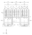
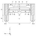
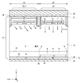
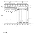
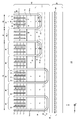
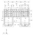
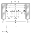
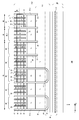
- FIG. 10 is an enlarged top view showing a mesa unit 60 in the transistor unit 70, the diode unit 80, and the boundary 90. It is a figure which shows an example of the structure of the semiconductor device 100 in the aa cross section of FIG. 10 is an enlarged view of a YZ cross section of the mesa unit 60.
- FIG. 15 is an enlarged view of another example of the YZ cross section of the mesa unit 60.
- FIG. 15 is an enlarged view of another example of the YZ cross section of the mesa unit 60.
- FIG. 15 is an enlarged view of another example of the YZ cross section of the mesa unit 60.
- FIG. 15 is an enlarged view of another example of the YZ cross section of the mesa unit 60.
- FIG. 7 is a view showing another example of the structure of the semiconductor device 100 in the aa cross section of FIG. 1;
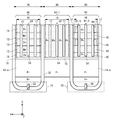
- FIG. 6 is a view showing another example of the upper surface of the semiconductor device 100. It is a figure which shows the aa cross section in FIG. It is a figure which shows the other example of the aa cross section in FIG. It is a figure which shows the other example of the aa cross section in FIG. 15 is an enlarged view of another example of the YZ cross section of the mesa unit 60.
- FIG. FIG. 6 is a view showing another example of the cross section aa in the semiconductor device 100.
- FIG. 6 is a view showing another example of the cross section aa in the semiconductor device 100.
- FIG. 15 is a view for explaining an operation example of the semiconductor device 100 shown in FIG. 14;
- FIG. 15 is a view for explaining an operation example of the semiconductor device 100 shown in FIG. 14;
- FIG. 6 is a view showing another example of the cross section aa in the semiconductor device 100.
- FIG. 6 is a view showing another example of the upper surface of the semiconductor device 100.
- FIG. 20 is an enlarged top view showing a mesa unit 60 in the transistor unit 70, the diode unit 80, and the boundary 90 of the semiconductor device 100 shown in FIG.
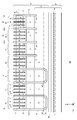
- FIG. 21 is a view showing an example of a bb cross section in the mesa unit 60 of the diode unit 80 shown in FIG. 20;
- FIG. 7 is a view showing an arrangement example of the first openings 61 on the upper surface of the mesa unit 60 of the diode unit 80.
- FIG. 17 is a view showing another example of the top surface structure of the transistor section 70, the diode section 80, and the mesa section 60 at the boundary section 90.
- FIG. 6 is a view showing another example of the bb cross section of the semiconductor device 100.
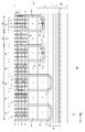
- FIG. 18 is a view showing another example of the top surface structure of the semiconductor device 100. It is a figure which shows an example of the aa cross section in FIG. It is a figure which shows an example of the doping concentration distribution in the Z-axis direction of the mesa part 60 of the transistor part 70, and the pillar area
- FIG. 18 is a view showing another example of the top surface structure of the semiconductor device 100. It is a figure which shows an example of the aa cross section in FIG. It is a figure which shows the YZ cross section of an example of the semiconductor device 200 which concerns on embodiment of this invention. It is a figure which shows the YZ cross section of an example of the semiconductor device 300 which concerns on embodiment of this invention.
- the first conductivity type is N-type and the second conductivity type is P-type is shown, but the first conductivity type may be P-type and the second conductivity type may be N-type.
- the conductivity types of the substrate, layer, region and the like in the respective embodiments have opposite polarities.
- FIG. 1 is a view partially showing an upper surface of a semiconductor device 100 according to an embodiment of the present invention.
- the semiconductor device 100 of this example is a semiconductor chip provided with a transistor unit 70 and a diode unit 80.
- the transistor unit 70 includes a transistor such as an IGBT.
- the diode unit 80 is provided adjacent to the transistor unit 70 on the upper surface of the semiconductor substrate, and includes a diode such as FWD (Free Wheel Diode).
- FWD Free Wheel Diode
- the gate metal layer 50 contacts the gate runner 48 through the contact hole 49.
- the gate runner 48 is formed of polysilicon doped with an impurity. Gate runner 48 is connected to the gate conductive portion in gate trench portion 40 on the upper surface of the semiconductor substrate. Gate runner 48 is not connected to the dummy conductive portion in dummy trench portion 30.
- the gate runner 48 of this example is formed from the lower side of the contact hole 49 to the tip of the gate trench portion 40.
- An insulating film such as an oxide film is formed between the gate runner 48 and the upper surface of the semiconductor substrate.
- the gate conductive portion is exposed at the top surface of the semiconductor substrate at the tip of the gate trench portion 40 and is in contact with the gate runner 48. In FIG. 1, there is a portion where the emitter electrode 52 and the gate runner 48 overlap in plan view, but the emitter electrode 52 and the gate runner 48 are electrically insulated from each other with an insulating film (not shown) interposed therebetween.
- Emitter electrode 52 and gate metal layer 50 are formed of a material containing a metal.
- each electrode is formed of aluminum or aluminum-silicon alloy.
- Each electrode may have a barrier metal formed of titanium, a titanium compound, or the like below the region formed of aluminum or the like, and may have a plug formed of tungsten or the like in the contact hole.
- a dummy trench portion 30 may be provided between the gate trench portion 40 of the transistor portion 70 and the boundary portion 90 or the diode portion 80.
- one or more gate trench sections 40 and one or more dummy trench sections 30 may be alternately formed along the arrangement direction.
- a plurality of dummy trench portions 30 are continuously arranged at predetermined intervals.
- the trench portion adjacent to the transistor portion 70 in the boundary portion 90 or the diode portion 80 may be the gate trench portion 40.
- the dummy trench portion 30 may have a U-shape on the upper surface of the semiconductor substrate 10 similarly to the gate trench portion 40. That is, the dummy trench portion 30 of this example has the two extending portions 29 extending along the extending direction and the connecting portion 31 connecting the two extending portions 29. In another example, dummy trench portion 30 may have a linear shape extending in the extending direction without connection portion 31. In the present specification, the straight extending portions (31, 29) of the respective trench portions are one trench portion.
- Emitter electrode 52 is formed above gate trench portion 40, dummy trench portion 30, well region 11, emitter region 12, base region 14 and contact region 15.
- the well region 11 is of the second conductivity type (P + type in this example), and is formed in a predetermined range from the end of the active region on the side where the gate metal layer 50 is provided.
- the diffusion depth of the well region 11 may be deeper than the depths of the gate trench portion 40 and the dummy trench portion 30.
- a partial region on the gate metal layer 50 side of the gate trench portion 40 and the dummy trench portion 30 is formed in the well region 11. The bottom of the end in the extension direction of the dummy trench portion 30 may be covered by the well region 11.
- a region sandwiched by the respective trench portions is referred to as a mesa portion 60.
- the mesa portion 60 may be a portion of the semiconductor substrate sandwiched between two adjacent trench portions, and may be a portion from the top surface of the semiconductor substrate to the deepest bottom of each trench portion.
- the mesa 60 at the boundary 90 may be referred to as a boundary mesa 60-1.
- a base region 14 is formed in the mesa portion 60.
- the base region 14 is a second conductivity type having a doping concentration lower than that of the well region 11.
- the base region 14 in this example is P-type.
- base regions 14-e are disposed at both ends in the X-axis direction of each mesa 60 (in FIG. 1, only one end in the X-axis direction is shown).
- a contact region 15 of the second conductivity type having a doping concentration higher than that of the base region 14 is selectively formed on the top surface of the mesa 60.
- the contact region 15 in this example is P + type.
- the emitter region 12 of the first conductivity type having a doping concentration higher than that of the semiconductor substrate is selectively formed on the upper surface of the mesa unit 60 of the transistor unit 70.
- the emitter region 12 in this example is N + type.
- the region adjacent to the base region 14-e on the top surface of each mesa 60 is the contact region 15.
- Emitter region 12 is provided adjacent to gate trench portion 40 on the top surface of mesa portion 60. In addition, a part of emitter region 12 may be provided adjacent to dummy trench portion 30.
- the contact region 15 of the transistor unit 70 may be provided adjacent to the emitter region 12 on the top surface of the mesa unit 60. Each of emitter region 12 and contact region 15 has a portion exposed from the insulating film by contact hole 54.
- the emitter region 12 and the contact region 15 in the transistor portion 70 of this example are provided in a stripe shape extending in the extending direction (X-axis direction) of the trench portion on the upper surface of the semiconductor substrate.
- the stripe shape indicates that the length in the extending direction (X-axis direction) of the trench portion is longer than the width in the arrangement direction (Y-axis direction) of the trench portion.
- the length and width may refer to the maximum length and the maximum width in the X-axis direction and the Y-axis direction.
- the stripe shape may refer to a shape whose length is twice or more of the width, may be 4 times or more, or 10 times or more.
- a plurality of contact holes 54 may be provided in each mesa portion 60.
- any one of the contact holes 54 is arranged such that the PN junction portion between the contact region 15 and the emitter region 12 is exposed from the insulating film.
- the contact holes 54 corresponding to the respective PN junction portions are disposed.
- the mesa portion 60 may be provided with a contact hole 54 for exposing the contact region 15 from the insulating film.
- a contact hole 54 is provided at a position facing the center of the contact region 15 in the Y-axis direction.
- the emitter region 12 is not formed in the mesa unit 60 of the diode unit 80 of this example.
- the contact region 15 or the base region 14 is formed from one dummy trench portion 30 sandwiching the mesa portion 60 to the other dummy trench portion 30. That is, on the upper surface of the semiconductor substrate, the width in the Y-axis direction of the mesa unit 60 of the diode unit 80 and the width in the Y-axis direction of the contact region 15 or the base region 14 provided in the mesa unit 60 of the diode unit 80 are equal.
- the contact area 15 is disposed in the area adjacent to the base area 14-e on the top surface of the mesa section 60. Further, the base region 14 is disposed in a region adjacent to the contact region 15 on the opposite side to the base region 14-e in the X-axis direction.
- a contact region 15 is provided on the entire top surface of the boundary mesa 60-1 of the boundary 90 between the base regions 14-e.
- the area of the contact region 15 exposed on the upper surface of one boundary mesa 60-1 may be larger than the area of the contact region 15 exposed on the upper surface of one mesa 60 of the diode unit 80.
- FIG. 1 shows an example in which the boundary mesa 60-1 in the boundary 90 is one, the boundary 90 has a plurality of boundary mesas 60-1 arranged in the Y-axis direction. May be
- the contact hole 54 is formed above the contact region 15 and the base region 14.
- the contact hole 54 is formed above the contact region 15 in the boundary mesa portion 60-1.
- Neither contact hole 54 is disposed above the base region 14-e and the well region 11 disposed at both ends of the mesa 60 in the X-axis direction.
- the diode section 80 has a cathode region 82 of the first conductivity type in the region on the lower surface side of the semiconductor substrate.
- the cathode region 82 in this example is N + type. In FIG. 1, the range in which the cathode region 82 is formed is indicated by a broken line.
- the diode section 80 may be an area where the cathode area 82 is projected on the upper surface of the semiconductor substrate.
- the region where the cathode region 82 is projected on the upper surface of the semiconductor substrate may be separated from the contact region 15 in the + X axis direction.
- a collector region of the second conductivity type may be formed in a region where the cathode region 82 is not formed in the region on the lower surface side of the semiconductor substrate.
- the transistor unit 70 may be a region in which a trench portion or a mesa portion is formed in a region obtained by projecting the collector region on the upper surface of the semiconductor substrate.
- a first storage region 16 of the first conductivity type and a second storage region 17 of the first conductivity type are provided in the semiconductor substrate.
- the first accumulation region 16 and the second accumulation region 17 are formed at different depths in the semiconductor substrate.
- the first accumulation region 16 and the second accumulation region 17 are not exposed to the upper surface of the semiconductor substrate.
- a range in which the first accumulation region 16 and the second accumulation region 17 are provided in a projection plane parallel to the upper surface of the semiconductor substrate is indicated by a broken line.
- the first accumulation area 16 and the second accumulation area 17 of this example are arranged in a stripe shape in the area between the two base areas 14-e arranged at both ends in the X-axis direction on the projection plane. ing.
- the first accumulation area 16 and the second accumulation area 17 are arranged such that a part of the areas overlap in the Z-axis direction.
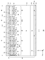
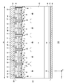
- FIG. 3 is a view showing an example of the structure of the semiconductor device 100 in the aa cross section of FIG.
- the aa cross section is a YZ plane passing through the emitter region 12 of the transistor section 70.
- the semiconductor device 100 of this example has the semiconductor substrate 10, the interlayer insulating film 38, the emitter electrode 52, and the collector electrode 24 in the cross section.
- Emitter electrode 52 is formed on the upper surface of semiconductor substrate 10 and interlayer insulating film 38.
- the semiconductor substrate 10 may be a silicon substrate, a silicon carbide substrate, or a nitride semiconductor substrate such as gallium nitride.
- the semiconductor substrate 10 of this example is a silicon substrate.
- the semiconductor substrate 10 includes the drift region 18 of the first conductivity type.
- the drift region 18 in this example is N-type.
- the drift region 18 may be a region remaining without forming other doping regions.
- the semiconductor substrate 10 is provided between the upper surface 21 of the semiconductor substrate 10 and the drift region 18, and is provided with a P ⁇ type base region 14 having a doping concentration lower than that of the contact region 15.
- the gate trench portion 40 and the dummy trench portion 30 are provided from the upper surface 21 of the semiconductor substrate 10 to the inside of the semiconductor substrate 10 (the drift region 18 in this example) through the base region 14.
- the emitter region 12, the contact region 15, the base region 14, the first accumulation region 16, the second accumulation region 17, and the middle region 62 are provided in the mesa portion 60 of the transistor portion 70.
- the base region 14 is provided adjacent to at least a first trench portion of the two trench portions sandwiching the mesa portion 60.
- the base region 14 in this example is provided adjacent to both of the two trench portions sandwiching the mesa portion 60.
- the accumulation region is a region in which a dopant of the same conductivity type as the drift region 18 (in this example, an N-type donor) is accumulated at a higher concentration than the drift region 18.
- Emitter region 12 is provided between upper surface 21 of semiconductor substrate 10 and base region 14 inside mesa 60. Emitter region 12 of this example is provided between base region 14 and upper surface 21 of semiconductor substrate 10 in a region adjacent to gate trench portion 40 or dummy trench portion 30.
- the contact region 15 is provided between the upper surface 21 of the semiconductor substrate 10 and the base region 14 inside the mesa portion 60.
- the contact region 15 in the present example is provided between the base region 14 and the upper surface 21 of the semiconductor substrate 10 in a region not adjacent to the gate trench portion 40 and the dummy trench portion 30.
- the first accumulation region 16 is an N + -type region having a doping concentration higher than that of the drift region 18.
- the first accumulation region 16 is provided between the base region 14 and the drift region 18.
- the first storage region 16 may be disposed with a gap between it and the first trench portion (e.g., the gate trench portion 40).
- the first storage region 16 of this example is disposed with a gap for both of the two trench portions disposed on both sides of the mesa portion 60.
- a region of the second conductivity type is provided between the first storage region 16 and the trench portion.
- a P-type base region 14 is disposed between the first storage region 16 and the trench portion.
- the second accumulation region 17 has a first opening 61 disposed at a deeper position than the first accumulation region 16 when viewed from the top surface of the semiconductor substrate 10.
- the first opening 61 in this example is provided at a position not overlapping the gap between the first storage region 16 and the trench portion. The first opening 61 penetrates the second accumulation region 17.
- the drift region 18 and the intermediate region 62 are connected via the first opening 61 provided in the second accumulation region 17. As shown in FIG. 3, the junction between the drift region 18 and the intermediate region 62 may be disposed inside the first opening 61. In another example, the junction of the drift region 18 and the intermediate region 62 may be disposed below the second accumulation region 17. In this case, an intermediate region 62 is formed in the entire inside of the first opening 61. In another example, the junction between the drift region 18 and the intermediate region 62 may be disposed above the second accumulation region 17. In this case, the drift region 18 is formed in the entire inside of the first opening 61.
- the emitter region 12 and the contact region 15 are not provided.
- the other structure is the same as that of the mesa unit 60 of the transistor unit 70. That is, in the mesa unit 60 of the diode unit 80, the base region 14, the first accumulation region 16, the second accumulation region 17, and the middle region 62 are provided.
- the base region 14 in the mesa unit 60 of the diode unit 80 is formed over the entire region between the first accumulation region 16 and the upper surface 21 of the semiconductor substrate 10 in the cross section.
- the carrier injection promoting effect (IE effect) can be enhanced and the on voltage can be reduced. Further, by arranging the first storage region 16 away from the trench portion, it is possible to reduce the transient collector-gate capacitance at the time of reverse recovery of the diode portion 80 or the like.
- the second accumulation region 17 By arranging the second accumulation region 17 so as to cover the gap between the first accumulation region 16 and the trench portion, excessive extraction of carriers can be suppressed in the region adjacent to the trench portion. Therefore, the IE effect can be maintained while reducing the collector-gate capacitance. Furthermore, by providing the first opening 61 in the second storage region 17, carriers can be stored in a region adjacent to the trench portion when the semiconductor device 100 is turned on or the like. The carrier can be pulled out through the opening 61 of the Therefore, the turn-off loss can be reduced while maintaining the IE effect. Note that at least one of the first accumulation region 16 and the second accumulation region 17 may not be provided in at least one of the diode portion 80 and the boundary portion 90.
- N + -type buffer region 20 is formed under the drift region 18 in each of the transistor portion 70, the diode portion 80 and the boundary portion 90.
- the doping concentration of buffer region 20 is higher than the doping concentration of drift region 18.
- Buffer region 20 may function as a field stop layer that prevents the depletion layer extending from the lower surface side of base region 14 from reaching P + type collector region 22 and N + type cathode region 82.
- a P + type collector region 22 is formed below the buffer region 20.
- an N + -type cathode region 82 is formed below the collector region 22.
- the collector region 22 may be formed below the buffer region 20, and the cathode region 82 may be formed.
- a collector region 22 is formed at the boundary 90 of this example.
- the diode section 80 is an area overlapping the cathode area 82 in the direction perpendicular to the lower surface 23 of the semiconductor substrate 10.
- the transistor portion 70 is a region overlapping with the collector region 22 in the direction perpendicular to the lower surface 23 of the semiconductor substrate 10, in which predetermined unit configurations including the emitter region 12 and the contact region 15 are regularly arranged.
- the emitter region 12 is not formed on the upper surface of the mesa portion 60
- the contact region 15 is formed on most of the upper surface of the mesa portion 60 (for example, half or more of the upper surface of the mesa portion 60). Area.
- One or more gate trench portions 40 and one or more dummy trench portions 30 are formed on the upper surface 21 of the semiconductor substrate 10.
- Each trench portion penetrates base region 14 from upper surface 21 of semiconductor substrate 10 to reach drift region 18.
- the drift region 18 may be reached.
- the fact that the trench portion penetrates the doping region is not limited to the one manufactured in the order of forming the doping region and then forming the trench portion. After forming the trench portion, those in which the doping region is formed adjacent to the trench portion are also included in those in which the trench portion penetrates the doping region.
- the gate trench portion 40 has a gate trench formed on the upper surface 21 of the semiconductor substrate 10, a gate insulating film 42, and a gate conductive portion 44.
- the gate insulating film 42 is formed to cover the inner wall of the gate trench.
- the gate insulating film 42 may be formed by oxidizing or nitriding the semiconductor on the inner wall of the gate trench.
- the gate conductive portion 44 is formed inside the gate insulating film 42 inside the gate trench. That is, the gate insulating film 42 insulates the gate conductive portion 44 and the semiconductor substrate 10.
- the gate conductive portion 44 is formed of a conductive material such as polysilicon.
- Gate conductive portion 44 includes a region facing at least adjacent base region 14 with gate insulating film 42 interposed therebetween in the depth direction.
- the gate trench portion 40 in the cross section is covered with the interlayer insulating film 38 on the upper surface of the semiconductor substrate 10.
- a predetermined voltage is applied to the gate conductive portion 44, a channel of the inversion layer of electrons is formed in the surface layer of the interface in the base region 14 in contact with the gate trench.
- the dummy trench portion 30 may have the same structure as the gate trench portion 40 in the cross section.
- the dummy trench portion 30 has a dummy trench formed on the upper surface side of the semiconductor substrate 10, a dummy insulating film 32 and a dummy conductive portion 34.
- the dummy insulating film 32 is formed to cover the inner wall of the dummy trench.
- the dummy conductive portion 34 is formed inside the dummy trench and is formed inside the dummy insulating film 32.
- the dummy insulating film 32 insulates the dummy conductive portion 34 and the semiconductor substrate 10.
- the dummy conductive portion 34 may be formed of the same material as the gate conductive portion 44.
- the dummy conductive portion 34 is formed of a conductive material such as polysilicon.
- the dummy conductive portion 34 may have the same length as the gate conductive portion 44 in the depth direction.
- the dummy trench portion 30 in the cross section is covered with the interlayer insulating film 38 on the upper surface 21 of the semiconductor substrate 10.
- the bottoms of the dummy trench portion 30 and the gate trench portion 40 may be curved downward (curved in cross section).
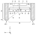
- FIG. 4 is an enlarged view of the YZ cross section of the mesa unit 60. As shown in FIG. In FIG. 4, the mesa unit 60 in the transistor unit 70 is shown. In the present example, the first trench portion is the gate trench portion 40-1, and the second trench portion is the gate trench portion 40-2.
- the first accumulation region 16 has a first gap 63 between itself and the gate trench portion 40-1.
- the first storage region 16 has a second gap 64 between it and the gate trench portion 40-2.
- a base region 14 may be formed in the first gap 63 and the second gap 64.
- the base region 14 and the middle region 62 are connected via the first gap 63 and the second gap 64.
- the second accumulation region 17 is disposed overlapping with both the first gap 63 and the second gap 64 in the depth direction of the semiconductor substrate 10.
- the second storage region 17 in this example is provided in contact with both the gate trench portion 40-1 and the gate trench portion 40-2.
- the second accumulation region 17 is arranged to at least cover the entire of the first gap 63 and the second gap 64.
- the first opening 61 is provided at a position not overlapping with both the first gap 63 and the second gap 64 in the depth direction of the semiconductor substrate 10.
- the first opening 61 of this example is disposed so as to include the center of the mesa 60 in the mesa width direction (that is, the direction connecting two trench parts, in this example, the Y-axis direction) in the opening.
- the distance between the first opening 61 and the gate trench portion 40 can be maximized, and the carriers accumulated in the vicinity of the gate trench portion 40 can be prevented from being drawn out through the first opening 61. Therefore, the on voltage of the semiconductor device 100 can be reduced.
- the width L2 of the first opening 61 is smaller than the width (M ⁇ L2) of the second accumulation region 17 in the mesa width direction.
- the width of the mesa portion 60 in the mesa width direction is M.
- the width L2 of the first opening 61 may be half or less, 1/4 or less, or 1/10 or less of the width (M ⁇ L2) of the second accumulation region 17. .
- the width L2 of the first opening 61 may be 1 ⁇ m or less, 0.5 ⁇ m or less, or 0.3 ⁇ m or less.
- the intermediate region 62 may be disposed to overlap the first opening 61 in the depth direction of the semiconductor substrate 10. That is, when the first opening 61 is viewed in the Z-axis direction from the lower surface 23 side of the semiconductor substrate 10, the intermediate region 62 may be arranged so that a part of the intermediate region 62 can be seen. Thereby, the carrier can be easily pulled out of the first opening 61 at the time of turn-off or the like. As shown in FIG. 4, the intermediate region 62 may be provided also inside the first opening 61.
- the width of the first gap 63 is L1, it is preferable to satisfy the following formula. 0 ⁇ L1 / M ⁇ 0.1
- the width of the second gap 64 may be the same as the width of the first gap 63. In order to reduce the gate-collector capacitance, the first storage region 16 and the gate trench portion 40 only need to be slightly apart. In addition, when the width L1 of the first gap 63 is increased, the carrier accumulation effect in the vicinity of the gate trench portion 40 is reduced.
- the upper limit of L1 / M may be 0.05 or 0.025.
- the lower limit of L1 / M may be 0.01 or 0.02.
- the mesa width M of the mesa unit 60 is approximately 1 ⁇ m to 10 ⁇ m.
- the width L1 of the first gap 63 may be 0.5 ⁇ m or less, may be 0.3 ⁇ m or less, and may be 0.1 ⁇ m or less.
- the thickness of the intermediate region 62 is T1
- the thickness of the base region 14 provided below the emitter region 12 is T2
- the thickness of the first storage region 16 is T3.
- the thickness of the second accumulation region 17 is T4.
- the width L 2 of the first opening 61 may be larger than the thickness T 1 of the middle region 62.
- the width L2 may be two or more times or three or more times the thickness T1. Since the intermediate region 62 is formed on substantially the entire mesa portion 60 in the XY plane, carriers can pass through even if the thickness in the Z-axis direction is small. On the other hand, if the width L2 of the first opening 61 is too small, carriers can not be efficiently extracted from the drift region 18.
- the thickness T2 of the base region 14 may be larger than the thickness T1 of the middle region 62.
- the thickness T2 of the base region 14 refers to the thickness of the region sandwiched between the emitter region 12 and the first accumulation region 16 in the depth direction. If the base region 14 is made too thin, the channel length becomes short, and the variation of the threshold voltage due to the positional variation of each doping region becomes large. Thickness T2 may be twice or more of thickness T1, and may be three or more times.
- the thickness T 3 of the first accumulation region 16 may be larger than the thickness T 1 of the middle region 62. Thickness T3 may be twice or more of thickness T1, and may be four or more times.
- the thickness T4 of the second accumulation region 17 may be larger than the thickness T1 of the middle region 62. The thickness T4 may be three or more times, or five or more times the thickness T1.
- a position at which the doping concentration of the drift region 18 is doubled may be a boundary between the second accumulation region 17 and the drift region 18.
- the carrier accumulation effect can be enhanced by increasing the thickness of each accumulation region.
- the thickness T 4 of the second accumulation region 17 may be larger than the thickness T 3 of the first accumulation region 16. Thereby, carriers can be efficiently accumulated near the lower end of the trench portion.
- the distance from the upper surface 21 of the semiconductor substrate 10 to the lower end of the first accumulation region 16 is D3, and from the lower end of the first accumulation region 16 to the second accumulation region 17
- the distance from the lower end of the second storage region 17 to the lower end of the gate trench portion 40 is D1.
- the distance D1 may be larger than the sum of the distance D2 and the distance D3.
- the distance D1 may be equal to or greater than 1.2 times or equal to or greater than 1.5 times the distances D2 + D3.
- the distance D3 may be larger than the distance D2.
- the distance D3 may be 1.5 times or more of the distance D2 or 2 times or more.
- the dummy trench portion 30 is not provided between the gate trench portions 40. That is, the plurality of gate trench portions 40 are continuously arranged in the Y-axis direction without sandwiching the dummy trench portion 30.
- a carrier accumulation effect can be produced.
- the characteristics of the semiconductor device 100 such as the switching speed can be adjusted.
- the depletion layer can be extended in the Y-axis direction to improve the withstand voltage of the semiconductor device 100.
- the carrier accumulation effect can be produced by providing the first accumulation region 16 and the second accumulation region 17. Further, by changing the width or the number of the first openings 61, the characteristics of the semiconductor device 100 such as the switching speed can be adjusted.
- the PN junction of the intermediate region 62 and the drift region 18 is provided in the vicinity of the first opening 61, the depletion layer can be expanded from the first opening 61. Therefore, the depletion layer can be extended in the Y-axis direction as in the case of the dummy trench portion 30.
- the man-hour of the screening test which tests whether the dummy insulating film 32 of the dummy trench part 30 has a predetermined characteristic etc. can be reduced.
- the second storage region 17 has a partial region at the same depth position as the base region 14 and another partial region at the same depth position as the drift region 18. It was provided. In another example, the second accumulation region 17 may be provided at the same depth position as the drift region 18 as a whole.
- first storage region 16 may be in contact with at least one of the two adjacent gate trench portions 40. That is, the first gap 63 may not be provided between the first storage region 16 and the at least one gate trench portion 40.
- At least a partial region of the first gap 63 and at least a partial region of the first opening 61 may be provided at a position overlapping in the Z-axis direction.
- the entirety of any one of the first gap 63 and the first opening 61 may be provided to overlap the other.
- both the first gap 63 and the first opening 61 may be in contact with the gate trench portion 40, or both may not be in contact, and only one of them is in contact with the gate trench portion 40. May be
- FIG. 5 is an enlarged view of another example of the YZ cross section of the mesa unit 60. As shown in FIG. In FIG. 4, the mesa unit 60 in the transistor unit 70 is shown.
- the gate trench portion 40 in the present example has an upper portion 46 and a lower portion 47.
- gate trench portion 40 is provided to extend on upper surface 21 of semiconductor substrate 10 along a predetermined extending direction (X-axis direction).
- the upper portion 46 is a portion where the side wall is formed in a straight line in a cross section (YZ plane) perpendicular to the extending direction.
- the side walls of the upper portion 46 adjacent to the upper surface 21 of the semiconductor substrate 10 may not be straight.
- the lower portion 47 is provided below the upper portion 46 and has a curved side wall.
- the lower portion 47 includes the lower end of the gate trench portion 40.
- the upper end of the lower portion 47 (the boundary with the upper portion 46) is a point at which the inclination of the side wall starts to change from the inclination of the side wall of the upper portion 46.
- the distance between the upper end of the side wall in the lower portion 47 and the intermediate region 62 is X, which is the shortest path 65 connecting the second accumulation region 17 without passing.
- the distance X may be larger than half of the width M of the mesa 60 (ie, may satisfy M / 2 ⁇ X).
- the distance X may be greater than 1.2 times half of the mesa width M and may be greater than 1.4 times.
- the distance of the shortest path connecting the lower end of the gate trench portion 40 and the middle region 62 may be X.
- the lower end of the gate trench portion 40 is a point located at the lowermost side in the gate trench portion 40.
- the lower end of the gate trench portion 40 may be disposed at the center of the gate trench portion 40 in the Y-axis direction.
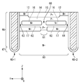
- FIG. 6 is an enlarged view of another example of the YZ cross section of the mesa unit 60. As shown in FIG. In the mesa unit 60 of this example, the arrangement of the intermediate region 62 is different from that of the mesa unit 60 shown in FIG. 4 or FIG. The other structure may be identical to the mesa 60 shown in FIG. 4 or FIG.
- the intermediate region 62 in this example is disposed so as not to overlap with the first opening 61 in the depth direction of the semiconductor substrate 10. That is, the end 66 of the first opening 61 is disposed outside the end 67 of the second accumulation area 17 between the first accumulation area 16 and the second accumulation area 17. The outside refers to the side closer to the adjacent gate trench portion 40.
- FIG. 7 is an enlarged view of another example of the YZ cross section of the mesa unit 60.
- the mesa unit 60 of this example differs from the mesa unit 60 shown in FIGS. 4 to 6 in the shape of the first storage region 16.
- Other structures may be identical to any of the mesas 60 shown in FIGS.
- the width Y2 in the Y-axis direction of the first opening 61 in the boundary mesa 60-1 is larger than the width Y1 of the first opening 61 in any mesa 60 of the transistor section 70.
- the width Y2 in the Y-axis direction of the first opening 61 in the boundary mesa 60-1 may be larger than the width Y1 of the first opening 61 in any mesa 60 of the transistor section 70. Accordingly, carriers such as holes can be efficiently extracted at the boundary between the transistor unit 70 and the diode unit 80. Therefore, in the transistor portion 70 and the diode portion 80, it is possible to suppress that one carrier affects the other.
- the width Y3 in the Y-axis direction of the first opening 61 in the diode unit 80 may be larger than the width Y1 of the first opening 61 in the mesa unit 60 of the transistor unit 70.
- the width Y 3 of the first opening 61 in the diode unit 80 may be larger as the mesa unit 60 is farther from the transistor unit 70.
- the width Y3 of the first opening 61 of at least a part of the mesa 60 in the diode section 80 may be larger than the width Y2 of the first opening 61 in the boundary mesa 60-1.
- FIG. 10 is a view showing a cross section aa in FIG.
- the aa cross section of this example is a YZ plane passing through the emitter region 12 of the transistor section 70.
- the aa cross section of this example is the semiconductor device 100 shown in FIGS. 1 to 8 in that the emitter region 12 is disposed adjacent to the two trench portions in the mesa portion 60 of the transistor portion 70. It is different.
- the other structure is the same as that of the semiconductor device 100 of any of the embodiments shown in FIGS. 1 to 8. Such a structure also makes it possible to easily achieve both the reduction of the on-state voltage and the reduction of the turn-off loss.
- FIG. 11 is a view showing another example of the cross section aa in FIG.
- the semiconductor device 100 of this example further includes a floating region 84 in addition to the configuration of the semiconductor device 100 described in any of FIGS. 1 to 10.
- the floating region 84 is formed above the cathode region 82 in the diode portion 80.
- Floating region 84 is formed to partially cover cathode region 82.
- the floating region 84 may be provided with a third opening 85. That is, a part of the cathode region 82 is not covered by the floating region 84. Thus, even if the floating region 84 is provided, the diode unit 80 can perform diode operation.
- the floating region 84 may be formed to cover an area larger than half of the top surface of the cathode region 82 in order to suppress the injection of electrons.
- the floating region 84 may not be disposed at a position overlapping the first opening 61. That is, the third opening 85 and the first opening 61 may be disposed at an overlapping position. In this case, electrons are injected from the cathode region 82 immediately below the first opening 61.
- FIG. 12 is a view showing another example of the cross section aa in FIG.
- the semiconductor device 100 of this example differs from the semiconductor device 100 shown in FIG. 11 in the arrangement of the floating regions 84.
- the other structure is the same as that of the semiconductor device 100 shown in FIG.
- the floating region 84 in this example is disposed at a position overlapping with the first opening 61. That is, the floating region 84 is disposed so that the third opening 85 and the first opening 61 do not overlap. In this case, electrons are injected from the cathode region 82 at a position shifted from the first opening 61 in the Y-axis direction.
- FIG. 13 is an enlarged view of another example of the YZ cross section of the mesa unit 60.
- the mesa portion 60 of this example differs from the gate trench portion 40 of any of the semiconductor devices 100 shown in FIGS. 1 to 12 in the structure of the gate trench portion 40.
- the other structure may be identical to any of the semiconductor devices 100 shown in FIGS.
- the gate trench portion 40 in the present example has a thin film portion 72 in which the gate insulating film 42 is thin, and a thick film portion 74 in which the gate insulating film 42 is thicker than the thin film portion 72.
- the thickness of the gate insulating film 42 may be the thickness in the Y-axis direction.
- the electron current is likely to spread to the center side of the mesa 60 by being attracted to the holes.
- the path length of the electron current in the P-type region is increased, and the on voltage is increased.
- the first accumulation region 16 and the middle region 62 be disposed to face the thin film portion 72.
- electrons are strongly attracted to the gate conductive portion 44, so that it is easy to flow an electron current along the gate trench portion 40.
- the second accumulation region 17 may be disposed to face the thin film portion 72, may be disposed to face the thick film portion 74, and may be disposed across both the thin film portion 72 and the thick film portion 74. Good.
- FIG. 14 is a view showing another example of the cross section aa in the semiconductor device 100.
- the semiconductor device 100 of this example is different from the semiconductor device 100 described in FIGS. 1 to 13 in the structure of the diode unit 80.
- the transistor portion 70 and the boundary portion 90 may be the same as the transistor portion 70 and the boundary portion 90 of any aspect described in FIGS. 1 to 13.
- the transistor portion 70 and the boundary portion 90 in the example of FIG. 14 are the same as the transistor portion 70 and the boundary portion 90 shown in FIG.
- the diode section 80 of this example is different from the diode section 80 shown in FIG. 10 in the structure of the second storage region 17.
- the other structure may be identical to that of the diode unit 80 shown in FIG.
- the second storage region 17 of the diode unit 80 in this example has the number per mesa unit 60 of the first opening 61 disposed along the Y-axis direction (mesa width direction) in the transistor unit 70.
- the number of first openings 61 arranged along the Y-axis direction is greater than the number per mesa 60.
- one first opening 61 is provided in each mesa 60 of the transistor unit 70, and a plurality of first openings 61 are formed in each mesa 60 of the diode 80. It is provided along the axial direction.
- any first opening 61 in each mesa unit 60 of the diode unit 80 may be disposed at a position corresponding to the first opening 61 in each mesa unit 60 of the transistor unit 70.
- the corresponding position indicates that the position in the Y-axis direction in the mesa unit 60 is the same.
- the first opening 61 of each mesa unit 60 of the transistor unit 70 is disposed at the center of each mesa unit 60 in the Y-axis direction, and any one of the mesa units 60 of the diode unit 80 is selected.
- the first opening 61 is also disposed at the center of each mesa 60 in the Y-axis direction.
- the arrangement of the first opening 61 in the boundary mesa 60-1 may be the same as the mesa 60 of the transistor 70, and may be the same as the mesa 60 of the diode 80.
- the transistor 70 and the diode It may be different from the part 80.
- the carrier accumulation effect at the time of ON can be maintained. Further, by providing more first openings 61 in the second accumulation region 17 of the diode unit 80, the amount of carrier injection from the anode side is increased, and the forward voltage of the diode unit 80 is reduced. it can. In addition, the carrier can be easily pulled out at the time of turn-off or the like. Further, the first openings 61 are dispersedly provided in the second accumulation region 17 of the diode unit 80, whereby the PN junctions can be dispersedly arranged in the Y-axis direction, and the origin of the spread of the depletion layer is dispersed. Can be provided. Therefore, the withstand voltage of the semiconductor device 100 can be improved.
- the number of first openings 61 in each mesa unit 60 of the diode unit 80 in the Y-axis direction may be the same or different. As an example, the number of the first openings 61 may be smaller as the mesa unit 60 has a larger distance from the transistor unit 70 in the Y-axis direction.
- the width La in the Y-axis direction of the second accumulation region 17 not in contact with the trench portion may be longer than the width Lb of the first opening 61. In this case, the amount of carriers injected from the anode side of the diode unit can be reduced to reduce the reverse recovery loss of the diode unit 80.
- the width La of the second accumulation region 17 not in contact with the trench portion in the Y-axis direction may be shorter than the width Lb of the first opening 61.
- PN junctions of the drift region 18 and the base region 14 can be distributed widely in the Y-axis direction, and a wide spread of the origin of the depletion layer can be provided. Therefore, the withstand voltage of the semiconductor device 100 can be improved.
- the end portion In the floating region 84 closest to the boundary portion 90, the end portion is in contact with the dummy trench portion 30 inside the mesa portion 60 projected onto the upper surface 21 of the semiconductor substrate 10 from the position of the end portion on the boundary portion 90 side.
- the length Wa to the Y-axis direction end of the second accumulation region 17 may be 5 ⁇ m or less.
- FIG. 15 is a view showing another example of the cross section aa in the semiconductor device 100. As shown in FIG. The semiconductor device 100 of this example differs from the semiconductor device 100 described in FIG. 14 in the structure of the diode unit 80.
- the transistor portion 70 and the boundary portion 90 may be the same as the transistor portion 70 and the boundary portion 90 of any aspect described in FIG.
- the floating region 84 has a third opening 85 overlapping the first opening 61-1 disposed at the center of the mesa 60 in the Y-axis direction.
- floating regions 84 discretely form a plurality of third openings 85 in one mesa 60 in the Y-axis direction so as to overlap with the respective first openings 61 of mesa 60. You may have. By overlapping and arranging the first opening 61 and the third opening 85, injection of the carrier can be promoted.
- FIG. 16 is a diagram for explaining an operation example of the semiconductor device 100 shown in FIG. FIG. 16 shows a state in which a forward bias is applied to the diode section 80. Also, in FIG. 16, the injection of holes is indicated by a solid arrow, and the injection of electrons is indicated by a broken arrow.
- the amount of holes injected from the anode side can be increased at the time of forward bias. Therefore, the forward bias of the diode unit 80 can be reduced.
- FIG. 17 is a diagram for explaining an operation example of the semiconductor device 100 shown in FIG. FIG. 17 shows a state in which the diode unit 80 is in reverse recovery.
- the plurality of first openings 61 are provided in the diode section 80, the amount of holes extracted from the anode side can be increased at the time of reverse recovery. Therefore, the reverse recovery time of the diode unit 80 can be shortened.
- the pn junction between the floating region 84 and the cathode region 82 is reverse biased and an avalanche current is generated due to avalanche breakdown. Therefore, holes flow from the pn junction toward the buffer region 20 and the drift region 18, and electrons flow from the pn junction toward the cathode region 82.
- the width of the third opening 85 in the Y-axis direction at the boundary between the boundary portion 90 and the diode portion 80 may be 5 ⁇ m or less.
- FIG. 18 is a view showing another example of the cross section aa in the semiconductor device 100. As shown in FIG. The semiconductor device 100 of this example is different from the semiconductor device 100 described in FIG. 15 in the structure of the diode unit 80.
- the transistor portion 70 and the boundary portion 90 may be the same as the transistor portion 70 and the boundary portion 90 of any aspect described in FIG.
- the diode section 80 of this example is different from the diode section 80 shown in FIG. 15 in the structure of the floating region 84.
- the other structure may be identical to that of the diode unit 80 shown in FIG.
- the floating region 84 in this example has a plurality of third openings 85 discretely in the Y-axis direction so as to overlap with the first openings 61 of the respective mesas 60. Thereby, injection of carriers at the time of forward bias can be promoted to further reduce the forward voltage.
- the corresponding first and second openings 61 and 85 may be disposed so as to partially overlap each other, or may be disposed so as to entirely overlap each other.
- FIG. 19 is a view showing another example of the upper surface of the semiconductor device 100.
- the semiconductor device 100 of this example is different from the semiconductor device 100 of any of the aspects described in FIGS. 1 to 18 in the structure of the diode unit 80.
- the other structure may be the same as that of the semiconductor device 100 of any aspect described in FIG. 1 to FIG.
- the structure other than the diode unit 80 is the same as that of the semiconductor device 100 shown in FIG.
- the upper surface of the semiconductor substrate 10 in each mesa portion 60 of the diode portion 80 of this example is closer to the P + -type contact region 15 and the contact region 15 along a direction (X-axis direction) perpendicular to the mesa width direction.
- Adjustment regions 19 with small hole mobility are alternately arranged.
- the adjustment region 19 may be a P-type region having a doping concentration lower than that of the contact region 15.
- the doping concentration of the adjustment region 19 may be the same as or different from that of the base region 14.
- the adjustment area 19 may be an N-type area.
- the doping concentration of the adjustment region 19 may be the same as or different from that of the emitter region 12.
- the amount of carriers injected into the drift region 18 of the diode unit 80 can be increased, and the forward voltage Vf of the diode unit 80 can be reduced.
- the forward voltage Vf can be reduced during large current operation.
- the area of the contact region 15 is increased, the peak value Irp of the reverse current flowing in the reverse recovery operation is increased.
- the forward voltage Vf of the diode unit 80 and the peak value Irp of the reverse current can be adjusted.
- contact region 15 in diode unit 80 may be provided at the same position and width in the X-axis direction with respect to contact region 15 in transistor unit 70.
- the adjustment region 19 may be provided at the same position and width in the X-axis direction with respect to the emitter region 12 of the transistor unit 70. These positions and widths may be positions and widths on the upper surface of the semiconductor substrate 10.
- contact region 15 in diode unit 80 may differ in at least one of the position and width in the X-axis direction from contact region 15 in transistor unit 70.
- the adjustment region 19 may be different from at least one of the position and the width in the X-axis direction with respect to the emitter region 12 of the transistor unit 70.
- FIG. 19 shows an example in which contact regions 15 and adjustment regions 19 are alternately arranged along the X-axis direction
- the arrangement of contact regions 15 and adjustment regions 19 is not limited to the example of FIG. Under the condition that each contact region 15 can be connected to emitter electrode 52 via contact hole 54, the arrangement of contact region 15 and adjustment region 19 can be changed.
- FIG. 21 is a view showing an example of the bb cross section in the mesa unit 60 of the diode unit 80 shown in FIG. As described above, the second accumulation area 17 is provided with the plurality of first openings 61.
- the first opening 61-1 closest to the dummy trench 30 among the plurality of first openings 61 is provided apart from the dummy trench 30.
- the first openings 61-1 may be provided so as not to overlap the first gaps 63, 64 in the Z-axis direction.
- the distance between the first opening 61-1 and the dummy trench portion 30 in the Y-axis direction may be twice or more or three times or more the width of the first gap 63 in the Y-axis direction. .
- the holes injected from the contact region 15 to the base region 14 are easier to pass through the first gaps 63 and 64 than passing through the first storage region 16. Most of the holes having passed through the first gaps 63 and 64 are injected into the drift region 18 through the first opening 61-1 closest to the dummy trench portion 30. Therefore, the number of holes passing through the first opening 61-2 most distant from the dummy trench portion 30 is smaller than the number of holes passing through the first opening 61-1.
- the first opening 61-2 may have a small width in the Y-axis direction because the amount of passing holes is relatively small. Even if the width in the Y-axis direction is small, the depletion layer can function as a starting point for spreading.
- the first opening 61-1 preferably has a certain width in order to allow holes to pass efficiently.
- FIG. 22 is a view showing an arrangement example of the first opening 61 on the upper surface of the mesa unit 60 of the diode unit 80.
- the respective first openings 61 in the mesa unit 60 of the diode unit 80 are formed continuously in the X-axis direction.
- the first openings 61-1 closest to the dummy trench portion 30 are discretely arranged in the X-axis direction.
- the first openings 61-2 may be provided continuously in the form of stripes along the X-axis direction.
- the first opening 61-2 may be formed longer than the first opening 61-1 in the X-axis direction.
- the first opening 61-2 may be formed continuously between the two contact regions 15 arranged at both ends in the X-axis direction in the mesa unit 60.
- the first opening 61-1 may be provided in a region overlapping with the contact region 15 in top view.
- the first opening 61-1 may be provided entirely in the area overlapping with the contact area 15, or a partial area may be provided in the area overlapping with the adjustment area 19. That is, the length of the first opening 61-1 in the X-axis direction may be smaller than the length of the contact region 15 in the X-axis direction, or may be equal to or greater than the length of the contact region 15 in the X-axis direction.
- FIG. 23 is a view showing another example of the top surface structure of the transistor portion 70, the diode portion 80 and the mesa portion 60 at the boundary portion 90.
- the adjustment area 19 is formed in a stripe shape along the X-axis direction.
- the shape of the adjustment region 19 may be the same as or different from the emitter region 12 of the transistor unit 70 shown in FIG.
- the width of the adjustment region 19 in the Y-axis direction may be the same as the width of the emitter region 12 in the Y-axis direction, and may be thin or wide.
- the area of the contact region 15 can be adjusted by adjusting the shape of the adjustment region 19.
- the structures of the transistor portion 70 and the boundary portion 90 may be the same as the transistor portion 70 and the boundary portion 90 of the semiconductor device 100 according to any one of the aspects described in FIGS. 1 to 22.
- the transistor portion 70 and the boundary portion 90 in the example of FIG. 23 have the same structure as the transistor portion 70 and the boundary portion 90 shown in FIG.
- FIG. 24 is a view showing another example of the bb cross section of the semiconductor device 100.
- the contact regions 15 are provided discretely along the Y-axis direction.
- Each contact region 15 may be provided in stripes along the X-axis direction, or may be provided discretely.
- Each contact region 15 is provided below the contact hole 54.
- the adjustment region other than the contact region 15 may be the base region 14 on the top surface of the mesa unit 60 of the diode unit 80.
- a P-type high concentration region 95 may be formed in a region in contact with the metal plug 94.
- the doping concentration of the high concentration region 95 is higher than the doping concentration of the contact region 15. Thereby, the contact resistance between the contact region 15 and the metal plug 94 can be reduced.
- the at least one first opening 61 may be provided at a position at least partially overlapping the contact region 15 in the Z-axis direction. In the example of FIG. 24, all the first openings 61 at least partially overlap any of the contact regions 15.
- FIG. 25 shows another example of the top surface structure of semiconductor device 100.
- the semiconductor device 100 of this example includes a pillar region 26 in place of the dummy trench portion 30 in the semiconductor device 100 described with reference to FIGS. 1 to 24.
- the pillar region 26 is a P-type region formed inside the semiconductor substrate 10.
- the other structure may be the same as that of the semiconductor device 100 of any aspect described in FIGS. 1 to 24.
- FIG. 25 shows a configuration in which a pillar region 26 is provided instead of the dummy trench portion 30 in the semiconductor device 100 shown in FIG.
- the pillar regions 26 are arranged along the Y-axis direction.
- the spacing in the Y-axis direction of the pillar region 26 in the present example is the same as the spacing of the extension portions 29 of the dummy trench portion 30 described in FIGS. 1 to 24.
- the distance between the pillar regions 26 in the Y-axis direction may be larger or smaller than the distance between the extension portions 39 of the gate trench portion 40.
- the width in the Y-axis direction of the pillar region 26 may be the same as or different from the width of the extension portion 39 of the gate trench portion 40.
- the shape in a top view of the pillar region 26 is, for example, a linear shape extending along the X-axis direction.
- the end of the pillar region 26 in the X-axis direction may be provided in the well region 11.
- the shape of the top view of the pillar region 26 may be U-shaped similarly to the dummy trench portion 30.
- FIG. 26 is a view showing an example of a cross section aa in FIG.
- the structure of the semiconductor device 100 according to this embodiment is the same as that of the semiconductor device 100 according to any one of the embodiments described with reference to FIGS. 1 to 24 except for the pillar region 26.
- the pillar region 26 is formed from the upper surface 21 of the semiconductor substrate 10 to reach the drift region 18.
- the upper end of the pillar region 26 may be covered by an interlayer insulating film 38. That is, the pillar region 26 may not be connected to the emitter electrode 52.
- the pillar region 26 may be in contact with the base region 14.
- the pillar region 26 provided in the transistor portion 70 may be sandwiched by an N-type high concentration region having a doping concentration higher than that of the drift region 18 on the upper surface of the semiconductor substrate 10.
- the high concentration region in this example is the emitter region 12.
- the pillar region 26 provided at the boundary between the transistor portion 70 and the boundary portion 90 is in contact with the emitter region 12 on the transistor portion 70 side, and may be in contact with the contact region 15 on the boundary portion 90 side.
- the pillar region 26 may be formed to the same depth position as the gate trench portion 40, may be formed to a deeper position, and may be formed to a shallower position.
- the length of the pillar region 26 in the Z-axis direction may be 80% or more and 120% or more of the length of the gate trench portion 40 in the Z-axis direction.
- the pillar region 26 is preferably formed to a position deeper than the second accumulation region 17.
- the pillar region 26 in this example is a P + -type having a doping concentration higher than that of the base region 14.
- the peak value of the doping concentration of the pillar region 26 may be 5.0 ⁇ 10 17 / cm 3 or more and 1.0 ⁇ 10 20 / cm 3 or less.
- the peak value of the doping concentration of the pillar region 26 may be the same as the peak value of the doping concentration of the contact region 15.
- the element regions such as the transistor portion 70 and the diode portion 80 in the semiconductor substrate 10 can be expanded. Further, by sandwiching the pillar region 26 with a high concentration N-type region such as the emitter region 12, the impedance of the pillar region 26 with respect to holes can be increased, and hole extraction can be suppressed.
- FIG. 27 is a diagram showing an example of the doping concentration distribution in the Z-axis direction of the mesa unit 60 of the transistor unit 70 and the pillar region 26. As shown in FIG. In the present example, first gaps 63, 64 are provided between the first accumulation region 16 and the pillar region 26.
- FIG. 27 shows the doping concentration distribution at the cross section c-c passing through the center of the pillar region 26 in the Y-axis direction.
- the doping concentration distribution in the Z-axis direction of the pillar region 26 may have a plurality of peaks.
- the doping concentration distribution has peaks at depth positions Z0, Z2 and Z4.
- the pillar region 26 may be formed by implanting P-type impurities at different depth positions and performing heat treatment. Thereby, the long pillar region 26 can be easily formed in the depth direction.
- the depth positions Z1 and Z3 at which the doping concentration distribution of the pillar region 26 has a minimum value may not overlap with the emitter region 12, the first storage region 16 and the second storage region 17. That is, neither of the depth positions Z1 and Z3 is included in the range of the depth position from the upper end to the lower end of the high concentration N-type region.
- At least one of the depth positions Z0, Z2, and Z4 at which the doping concentration distribution has a peak value may be provided at a position overlapping the emitter region 12, the first accumulation region 16, and the second accumulation region 17. That is, at least one of the depth positions Z0, Z2, and Z4 is included in the range of the depth position from the upper end to the lower end of the high concentration N-type region.
- the pillar region 26 by arranging the region having a low doping concentration not to oppose the high concentration N-type region, the diffusion of the N-type impurity into the pillar region 26 can be suppressed. Therefore, the width of the pillar region 26 in the Y-axis direction can be maintained at a certain level or more.
- the depths of the second accumulation region 17 and the first accumulation region 16 may be made to substantially coincide with the depths where the width of the pillar region 26 is locally narrow.
- FIG. 29 is a view showing another example of the cross section aa in FIG.
- the semiconductor device 100 of this example is different from the example of FIG. 26 in that a part of the upper end of the pillar region 26 is not covered with the interlayer insulating film 38. That is, the upper end of the pillar region 26 is connected to the emitter electrode 52.
- the other structure may be the same as that of the semiconductor device 100 of any aspect described in FIGS. 26 and 27. Also in this case, holes can be injected into and drawn out of the drift region 18 through the pillar region 26.
- FIG. 31 is a view showing an example of an aa cross section in FIG.
- the semiconductor device 100 of this example differs from the semiconductor device 100 shown in FIG. 26 in the structure of the transistor unit 70.
- the structure of the transistor unit 70 of this example is the same as that of the transistor unit 70 shown in FIG.
- the structure other than the transistor unit 70 is the same as that of the semiconductor device 100 described in FIG.
- the semiconductor device 100 described in FIGS. 25 to 31 may not include the first storage region 16 and the second storage region 17.
- FIG. 32 is a view showing a YZ cross section of an example of the semiconductor device 200 according to the embodiment of the present invention.
- the semiconductor device 200 includes the transistor unit 70 described in FIGS. 1 to 31.
- the semiconductor device 200 does not include the diode portion 80 and the boundary portion 90.
- the transistor unit 70 is the same as the transistor unit 70 in any of the modes described in FIGS. 1 to 31.
- connection portion 26 pillar region 27 high concentration region 29 extension portion 30 dummy trench portion 31 connection portion 32 32 Dummy insulating film, 34: dummy conductive portion, 38: interlayer insulating film, 39: extended portion, 40: gate trench portion, 41: connection portion, 42: gate insulating film, 44: Gate conductive part, 46: Upper part, 47: Lower side Minute, 48: gate runner, 49: contact hole, 50: gate metal layer, 52: emitter electrode, 54: contact hole, 56: contact hole, 60: mesa Part 61: first opening 62: intermediate region 63: first gap 64: second gap 65: shortest path 66: end , 67: end part, 68: second opening, 70: transistor part, 72: thin film part, 74: thick film part, 80:
Landscapes
- Metal-Oxide And Bipolar Metal-Oxide Semiconductor Integrated Circuits (AREA)
- Electrodes Of Semiconductors (AREA)
Abstract
第1導電型のドリフト領域を有する半導体基板と、半導体基板の上面から半導体基板の内部まで設けられた第1のトレンチ部と、半導体基板の上面とドリフト領域との間において第1のトレンチ部と隣接して設けられた第2導電型のベース領域と、ベース領域とドリフト領域との間に設けられ、ドリフト領域よりもドーピング濃度の高い第1導電型の第1の蓄積領域と、第1の蓄積領域より深い位置に設けられた、ドリフト領域よりもドーピング濃度の高い第1導電型の第2の蓄積領域と、第1の蓄積領域と第2の蓄積領域との間に設けられた第2導電型の中間領域とを備え、第2の蓄積領域は、第1の蓄積領域より深い位置に設けられた第1の開口部を有する半導体装置を提供する。
Description
本発明は、半導体装置に関する。
従来、絶縁ゲート型バイポーラトランジスタ(IGBT)等の半導体装置において、チャネルとして機能するP型のベース領域の下に、高濃度のN型領域を設ける構成が知られている(例えば、特許文献1参照)。また、おもて面側にn+ソース層とトレンチを備えた逆導通IGBT(RC‐IGBT)が知られている(例えば、特許文献2参照)。
特許文献1 特開2014-197702号公報
特許文献2 特開平11-97715号公報
特許文献1 特開2014-197702号公報
特許文献2 特開平11-97715号公報
半導体装置は、耐圧等の特性がよいことが好ましい。
上記課題を解決するために、本発明の一つの態様においては、第1導電型のドリフト領域を有する半導体基板を備える半導体装置を提供する。半導体装置は、半導体基板の上面から前記半導体基板の内部まで設けられた第1のトレンチ部を備えてよい。半導体装置は、半導体基板の上面とドリフト領域との間において第1のトレンチ部と隣接して設けられた第2導電型のベース領域を備えてよい。半導体装置は、ベース領域とドリフト領域との間に設けられ、ドリフト領域よりもドーピング濃度の高い第1導電型の第1の蓄積領域を備えてよい。半導体装置は、第1の蓄積領域より深い位置に設けられた、ドリフト領域よりもドーピング濃度の高い第1導電型の第2の蓄積領域を備えてよい。半導体装置は、第1の蓄積領域と第2の蓄積領域との間に設けられた第2導電型の中間領域を備えてよい。第2の蓄積領域は、第1の蓄積領域より深い位置に設けられた第1の開口部を有してよい。
第1の蓄積領域は、第1のトレンチ部との間に第1の間隙を有してよい。第2の蓄積領域は、半導体基板の深さ方向において第1の間隙と重なって設けられてよい。第1の開口部は第1の間隙と重ならない位置に設けられてよい。
半導体装置は、半導体基板の上面から半導体基板の内部まで設けられ、且つ、第1のトレンチ部と対向する第2のトレンチ部を備えてよい。第1の蓄積領域は、第2のトレンチ部との間に第2の間隙を有してよい。第2の蓄積領域は、半導体基板の深さ方向において第2の間隙と重って設けられてよい。第1の開口部は、半導体基板の深さ方向において第2の間隙と重ならない位置に設けられていてよい。
第1のトレンチ部はゲートトレンチ部であってよい。半導体装置は、半導体基板の上面とベース領域との間において第1のトレンチ部と隣接して設けられ、ドリフト領域よりもドーピング濃度の高い第1導電型のエミッタ領域を備えてよい。
半導体基板の内部において第1のトレンチ部および第2のトレンチ部に挟まれた領域をメサ部としてよい。第1のトレンチ部および第2のトレンチ部を結ぶ方向をメサ幅方向としてよい。メサ幅方向において、第1の開口部の幅が、第2の蓄積領域の幅よりも小さくてよい。
第1の開口部が、メサ部のメサ幅方向における中央を含むように配置されていてよい。中間領域は、半導体基板の深さ方向において第1の開口部と重なってよい。中間領域は、第1の開口部の内部にも設けられていてよい。
中間領域は、第1の開口部を通って、第2の蓄積領域よりも下側に突出して設けられていてよい。中間領域は、半導体基板の深さ方向において第1の開口部と重ならないように配置されていてよい。第1の蓄積領域は、第1の開口部と重なる領域に、第2の開口部を有してよい。
メサ幅方向において、第1の間隙の幅をL1とし、メサ部の幅をMとした場合に、0<L1/M≦0.1であってよい。第1のトレンチ部は、半導体基板の上面において予め定められた延伸方向に沿って延伸して設けられてよい。第1のトレンチ部は、延伸方向と垂直な断面において、側壁が直線状に形成された上側部分を有してよい。第1のトレンチ部は、上側部分の下側に設けられ側壁が曲線状に形成された下側部分を有してよい。延伸方向と垂直な断面において、第1のトレンチ部の下側部分の上端と、中間領域とを、第2の蓄積領域を通過せずに結ぶ最短経路の距離をXとし、メサ部の幅をMとした場合に、M/2<Xであってよい。
メサ幅方向において、第1の間隙の幅をL1とし、第1の開口部の幅をL2とした場合に、L1<L2であってよい。メサ幅方向において、第1の間隙および第1の開口部の間の距離をL3とし、メサ部の幅をMとした場合に、0.9×M/2≦L3であってよい。
メサ幅方向における第1の開口部の幅が、半導体基板の上面と垂直な深さ方向における中間領域の厚みより大きくてよい。半導体基板の上面と垂直な深さ方向において、エミッタ領域の下側に設けられたベース領域の厚みが、中間領域の厚みより大きくてよい。
半導体基板の上面と垂直な深さ方向において、第1の蓄積領域の厚みが、中間領域の厚みより大きくてよい。半導体基板の上面と垂直な深さ方向において、第2の蓄積領域の厚みが、中間領域の厚みより大きくいてよい。
半導体基板は、ゲートトレンチ部を含むトランジスタ部と、ダイオードが形成されたダイオード部とを含んでよい。ダイオード部は、半導体基板の上面から半導体基板の内部まで設けられたダミートレンチ部を複数有してよい。ダイオード部の半導体基板の内部においてダミートレンチ部に挟まれた領域をメサ部とした場合に、ダイオード部のメサ部は、ベース領域、第1の蓄積領域、第2の蓄積領域および中間領域を有してよい。
半導体基板は、トランジスタ部と、ダイオード部との間に配置された境界メサ部を備えてよい。境界メサ部は、ベース領域、第1の蓄積領域、第2の蓄積領域および中間領域を有してよい。境界メサ部における第1の開口部の幅は、トランジスタ部のいずれかのメサ部における第1の開口部の幅よりも大きくてよい。ダイオード部のメサ部における第1の開口部の幅は、トランジスタ部のメサ部における第1の開口部の幅よりも大きくてよい。
半導体装置は、半導体基板の下面に配置されたコレクタ電極を備えてよい。半導体装置は、トランジスタ部の半導体基板の内部に設けられ、コレクタ電極と電気的に接続されている第2導電型のコレクタ領域を備えてよい。半導体装置は、ダイオード部の半導体基板の内部に設けられ、コレクタ電極と電気的に接続されている第1導電型のカソード領域を備えてよい。半導体装置は、半導体基板の内部において、カソード領域の上方に形成され、コレクタ電極と接触していない、第2導電型のフローティング領域を備えてよい。
フローティング領域は第3の開口部を有してよい。第3の開口部は、ダイオード部の第2の蓄積領域に設けられた第1の開口部と重なる位置に配置されていてよい。ダイオード部の第2の蓄積領域に設けられた第1の開口部の個数は、トランジスタ部の第2の蓄積領域に設けられた第1の開口部の個数よりも多くてよい。
半導体基板の内部において2つのダミートレンチ部に挟まれた領域をメサ部としてよい。2つのダミートレンチ部を結ぶ方向をメサ幅方向としてよい。ダイオード部の第2の蓄積領域において、メサ幅方向に沿って複数の第1の開口部が配置されていてよい。
ダイオード部の第2の蓄積領域においてメサ幅方向に沿って配置された複数の第1の開口部のうち、ダミートレンチ部に最も近い第1の開口部の幅が、ダミートレンチ部から最も離れた第1の開口部の幅より大きくてよい。
ダイオード部のメサ部における半導体基板の上面には、メサ幅方向とは垂直な方向に沿って第2導電型のコンタクト領域と、コンタクト領域よりも正孔の移動度が小さい調整領域とが交互に配置されてよい。ダイオード部の第2の蓄積領域においてメサ幅方向に沿って配置された複数の第1の開口部のうち、ダミートレンチ部に最も近い第1の開口部は、コンタクト領域と重なるように、メサ幅方向と垂直な方向に沿って離散的に配置されていてよい。
半導体基板は、ダイオードが形成されたダイオード部を更に備えてよい。ダイオード部は、ベース領域を有してよい。ダイオード部は、第1の蓄積領域を有してよい。ダイオード部は、第2の蓄積領域を有してよい。ダイオード部は、中間領域を有してよい。ダイオード部は、ベース領域と接して、且つ、半導体基板の上面からドリフト領域まで形成された、ベース領域よりもドーピング濃度の高い第2導電型のピラー領域を有してよい。
半導体基板の上面において、ピラー領域は、ドリフト領域よりもドーピング濃度の高い高濃度領域に挟まれていてよい。半導体基板の深さ方向におけるピラー領域のドーピング濃度分布は複数のピークを有してよい。
ピラー領域のドーピング濃度分布が極小値となる深さ位置は、第2の蓄積領域とは重ならなくてよい。ピラー領域のドーピング濃度のピーク値は、5.0×10¹⁷/cm3以上、1.0×1020/cm3以下であってよい。
なお、上記の発明の概要は、本発明の必要な特徴の全てを列挙したものではない。また、これらの特徴群のサブコンビネーションもまた、発明となりうる。
以下、発明の実施の形態を通じて本発明を説明するが、以下の実施形態は請求の範囲にかかる発明を限定するものではない。また、実施形態の中で説明されている特徴の組み合わせの全てが発明の解決手段に必須であるとは限らない。
本明細書においては半導体基板の深さ方向と平行な方向における一方の側を「上」、他方の側を「下」と称する。基板、層またはその他の部材の2つの主面のうち、一方の面を上面、他方の面を下面と称する。「上」、「下」の方向は重力方向、または、半導体装置の実装時における基板等への取り付け方向に限定されない。
本明細書では、X軸、Y軸およびZ軸の直交座標軸を用いて技術的事項を説明する場合がある。本明細書では、半導体基板の上面と平行な面をXY面とし、半導体基板の上面と垂直な深さ方向をZ軸とする。
各実施例においては、第1導電型をN型、第2導電型をP型とした例を示しているが、第1導電型をP型、第2導電型をN型としてもよい。この場合、各実施例における基板、層、領域等の導電型は、それぞれ逆の極性となる。
本明細書においてドーピング濃度とは、ドナーまたはアクセプタ化した不純物の濃度を指す。本明細書において、ドナーおよびアクセプタの濃度差をドーピング濃度とする場合がある。また、ドーピング領域におけるドーピング濃度分布のピーク値を、当該ドーピング領域におけるドーピング濃度とする場合がある。
図1は、本発明の実施形態に係る半導体装置100の上面を部分的に示す図である。本例の半導体装置100は、トランジスタ部70およびダイオード部80を備える半導体チップである。トランジスタ部70は、IGBT等のトランジスタを含む。ダイオード部80は、半導体基板の上面においてトランジスタ部70と隣接して設けられ、FWD(Free Wheel Diode)等のダイオードを含む。図1においてはチップ端部周辺のチップ上面を示しており、他の領域を省略している。
半導体基板の上面においてトランジスタ部70およびダイオード部80は、所定の配列方向(図1の例ではY軸方向)に沿って交互に配列されてよい。また、半導体装置100は、半導体基板の上面においてトランジスタ部70およびダイオード部80の境界に配置された境界部90を更に備えてよい。
図1においては半導体装置100における半導体基板の活性領域を示すが、半導体装置100は、活性領域を囲んでエッジ終端構造部を有してよい。活性領域は、半導体装置100をオン状態に制御した場合に電流が流れる領域を指す。エッジ終端構造部は、半導体基板の上面側の電界集中を緩和する。エッジ終端構造部は、例えばガードリング、フィールドプレート、リサーフおよびこれらを組み合わせた構造を有する。
本例の半導体装置100は、半導体基板の内部に設けられ、且つ、半導体基板の上面に露出するゲートトレンチ部40、ダミートレンチ部30、ウェル領域11、エミッタ領域12、ベース領域14およびコンタクト領域15を備える。また、本例の半導体装置100は、半導体基板の上面の上方に設けられたエミッタ電極52およびゲート金属層50を備える。エミッタ電極52およびゲート金属層50は互いに分離して設けられる。
エミッタ電極52およびゲート金属層50と、半導体基板の上面との間には層間絶縁膜が形成されるが、図1では省略している。本例の層間絶縁膜には、コンタクトホール56、コンタクトホール49およびコンタクトホール54が、当該層間絶縁膜を貫通して形成される。
エミッタ電極52は、コンタクトホール54を通って、半導体基板の上面におけるエミッタ領域12、コンタクト領域15およびベース領域14と接触する。また、エミッタ電極52は、コンタクトホール56を通って、ダミートレンチ部30内のダミー導電部と接続される。エミッタ電極52とダミー導電部との間には、不純物がドープされたポリシリコン等の、導電性を有する材料で形成された接続部25が設けられてよい。接続部25と半導体基板の上面との間には、酸化膜等の絶縁膜が形成される。
ゲート金属層50は、コンタクトホール49を通って、ゲートランナー48と接触する。ゲートランナー48は、不純物がドープされたポリシリコン等で形成される。ゲートランナー48は、半導体基板の上面において、ゲートトレンチ部40内のゲート導電部と接続される。ゲートランナー48は、ダミートレンチ部30内のダミー導電部とは接続されない。本例のゲートランナー48は、コンタクトホール49の下方から、ゲートトレンチ部40の先端部まで形成される。ゲートランナー48と半導体基板の上面との間には、酸化膜等の絶縁膜が形成される。ゲートトレンチ部40の先端部においてゲート導電部は半導体基板の上面に露出しており、ゲートランナー48と接触する。なお、図1では平面視で、エミッタ電極52とゲートランナー48が重なっている箇所があるが、エミッタ電極52とゲートランナー48は図示しない絶縁膜を挟んで互いに電気的に絶縁している。
エミッタ電極52およびゲート金属層50は、金属を含む材料で形成される。例えば、各電極の少なくとも一部の領域はアルミニウムまたはアルミニウム‐シリコン合金で形成される。各電極は、アルミニウム等で形成された領域の下層にチタンやチタン化合物等で形成されたバリアメタルを有してよく、コンタクトホール内においてタングステン等で形成されたプラグを有してもよい。
1つ以上のゲートトレンチ部40および1つ以上のダミートレンチ部30は、半導体基板の上面において所定の配列方向(本例ではY軸方向)に沿って所定の間隔で配列される。本例のトランジスタ部70は、連続して配列された複数のゲートトレンチ部40を有する。本例のトランジスタ部70は、境界部90またはダイオード部80に隣接する領域にダミートレンチ部30を有する。トランジスタ部70において、境界部90またはダイオード部80に隣接しない領域には、ダミートレンチ部30が設けられていない。つまり本例では、それぞれのトランジスタ部70において、ゲートトレンチ部40の間には、ダミートレンチ部30が設けられていない。トランジスタ部70のゲートトレンチ部40と、境界部90またはダイオード部80との間には、ダミートレンチ部30が設けられてよい。他の例のトランジスタ部70においては、配列方向に沿って1つ以上のゲートトレンチ部40と、1つ以上のダミートレンチ部30とが交互に形成されてもよい。
境界部90およびダイオード部80には、複数のダミートレンチ部30が所定の間隔で連続して配列されている。境界部90またはダイオード部80においてトランジスタ部70と隣接するトレンチ部は、ゲートトレンチ部40であってもよい。
ゲートトレンチ部40は、半導体基板の上面に平行であって配列方向と垂直な延伸方向(本例ではX軸方向)に沿って延伸する2つの延伸部分39と、2つの延伸部分39を接続する接続部分41を有してよい。接続部分41の少なくとも一部は曲線状に形成されることが好ましい。ゲートトレンチ部40の2つの延伸部分39の端部を接続することで、延伸部分39の端部における電界集中を緩和できる。ゲートランナー48は、ゲートトレンチ部40の接続部分41において、ゲートトレンチ部40の内部に設けられたゲート導電部と接続してよい。
ダミートレンチ部30は、ゲートトレンチ部40と同様に半導体基板10の上面においてU字形状を有してよい。つまり、本例のダミートレンチ部30は、延伸方向に沿って延伸する2つの延伸部分29と、2つの延伸部分29を接続する接続部分31を有する。他の例においては、ダミートレンチ部30は、接続部分31を有さずに延伸方向に延伸する直線形状を有してもよい。なお本明細書では、それぞれのトレンチ部の直線状の延伸部分(31、29)を、1つのトレンチ部としている。
エミッタ電極52は、ゲートトレンチ部40、ダミートレンチ部30、ウェル領域11、エミッタ領域12、ベース領域14およびコンタクト領域15の上方に形成される。ウェル領域11は第2導電型(本例ではP+型)であり、ゲート金属層50が設けられる側の活性領域の端部から、所定の範囲で形成される。ウェル領域11の拡散深さは、ゲートトレンチ部40およびダミートレンチ部30の深さよりも深くてよい。ゲートトレンチ部40およびダミートレンチ部30の、ゲート金属層50側の一部の領域はウェル領域11に形成される。ダミートレンチ部30の延伸方向の端の底は、ウェル領域11に覆われていてよい。
各トレンチ部に挟まれた領域をメサ部60と称する。メサ部60とは、隣り合う2つのトレンチ部に挟まれた半導体基板の部分であって、半導体基板の上面から、各トレンチ部の最も深い底部の深さまでの部分であってよい。本明細書では、境界部90におけるメサ部60を、境界メサ部60-1と称する場合がある。メサ部60には、ベース領域14が形成される。ベース領域14は、ウェル領域11よりもドーピング濃度の低い第2導電型である。本例のベース領域14はP-型である。本例では、各メサ部60のX軸方向における両端部には、ベース領域14-eが配置されている(図1においては、X軸方向の一方の端部のみを示している)。
メサ部60の上面には、ベース領域14よりもドーピング濃度の高い第2導電型のコンタクト領域15が選択的に形成される。本例のコンタクト領域15はP+型である。また、トランジスタ部70のメサ部60の上面には、半導体基板よりもドーピング濃度が高い第1導電型のエミッタ領域12が選択的に形成される。本例のエミッタ領域12はN+型である。本例では、それぞれのメサ部60の上面において、ベース領域14-eに隣接する領域は、コンタクト領域15である。
エミッタ領域12は、メサ部60の上面においてゲートトレンチ部40と隣接して設けられる。また、一部のエミッタ領域12は、ダミートレンチ部30と隣接して設けられてもよい。
トランジスタ部70のコンタクト領域15は、メサ部60の上面においてエミッタ領域12と隣接して設けられてよい。エミッタ領域12およびコンタクト領域15のそれぞれは、コンタクトホール54により絶縁膜から露出する部分を有する。
本例のトランジスタ部70におけるエミッタ領域12およびコンタクト領域15は、半導体基板の上面においてトレンチ部の延伸方向(X軸方向)に延伸するストライプ形状に設けられている。ストライプ形状とは、トレンチ部の延伸方向(X軸方向)における長さが、トレンチ部の配列方向(Y軸方向)における幅よりも長いことを指す。長さおよび幅は、X軸方向およびY軸方向における最大の長さおよび最大の幅を指してよい。ストライプ形状とは、当該長さが、当該幅の2倍以上の形状を指してよく、4倍以上の形状を指してよく、10倍以上の形状を指してもよい。
図1の例では、トランジスタ部70の各メサ部60において、ストライプ状のエミッタ領域12が、ゲートトレンチ部40の延伸部分39と隣接して設けられている。つまり、ストライプ状のエミッタ領域12が、各メサ部60のY軸方向の両端に配置されている。コンタクト領域15は、エミッタ領域12に挟まれて配置されている。なお、X軸方向において、エミッタ領域12とベース領域14-eとの間には、コンタクト領域15が設けられてよい。
それぞれのメサ部60に、コンタクトホール54が複数設けられてよい。一例として、トランジスタ部70の各メサ部60において、いずれかのコンタクトホール54は、コンタクト領域15とエミッタ領域12とのPN接合部分が絶縁膜から露出するように配置される。本例では、トランジスタ部70のそれぞれのメサ部60の上面に2つのPN接合部分が形成されるので、それぞれのPN接合部分に対応するコンタクトホール54が配置されている。また、メサ部60には、コンタクト領域15を絶縁膜から露出させるコンタクトホール54が設けられていてもよい。本例では、Y軸方向におけるコンタクト領域15の中央と対向する位置に、コンタクトホール54が設けられている。
本例のダイオード部80のメサ部60には、エミッタ領域12が形成されていない。ダイオード部80のメサ部60には、コンタクト領域15またはベース領域14が、メサ部60を挟む一方のダミートレンチ部30から、他方のダミートレンチ部30に渡って形成されている。つまり、半導体基板の上面において、ダイオード部80のメサ部60のY軸方向の幅と、ダイオード部80のメサ部60に設けられたコンタクト領域15またはベース領域14のY軸方向の幅は等しい。図1のダイオード部80の例では、メサ部60の上面においてベース領域14-eと隣接する領域にコンタクト領域15が配置されている。また、ベース領域14-eとはX軸方向の逆側においてコンタクト領域15と隣接する領域にベース領域14が配置されている。
境界部90の境界メサ部60-1の上面には、ベース領域14-eに挟まれた領域全体にコンタクト領域15が設けられている。一つの境界メサ部60-1の上面に露出するコンタクト領域15の面積は、ダイオード部80の一つのメサ部60の上面に露出するコンタクト領域15の面積より大きくてよい。なお、図1では境界部90における境界メサ部60-1が一つである例を示しているが、境界部90は、Y軸方向において配列された複数の境界メサ部60-1を有してもよい。
ダイオード部80において、コンタクトホール54は、コンタクト領域15およびベース領域14の上方に形成される。境界メサ部60-1においてコンタクトホール54は、コンタクト領域15の上方に形成される。いずれのコンタクトホール54も、メサ部60のX軸方向両端に配置されたベース領域14-eおよびウェル領域11の上方には配置されていない。
なおダイオード部80は、半導体基板の下面側の領域において、第1導電型のカソード領域82を有する。本例のカソード領域82はN+型である。図1においては、カソード領域82が形成される範囲を破線で示している。ダイオード部80は、カソード領域82を半導体基板の上面に投影した領域であってよい。カソード領域82を半導体基板の上面に投影した領域は、コンタクト領域15から+X軸方向に離れていてよい。半導体基板の下面側の領域において、カソード領域82が形成されていない領域には、第2導電型のコレクタ領域が形成されてよい。トランジスタ部70は、コレクタ領域を半導体基板の上面に投影した領域のうち、トレンチ部またはメサ部が形成されている領域であってよい。
図2は、トランジスタ部70、ダイオード部80および境界部90におけるメサ部60を拡大して示す上面図である。図2に示すトランジスタ部70のメサ部60は、ダミートレンチ部30に挟まれたメサ部60であるが、ゲートトレンチ部40に隣接するメサ部60も同様の構造を有する。
それぞれのメサ部60において、半導体基板の内部には、第1導電型の第1の蓄積領域16と、第1導電型の第2の蓄積領域17とが設けられている。第1の蓄積領域16および第2の蓄積領域17は、半導体基板の内部において異なる深さ位置に形成されている。第1の蓄積領域16および第2の蓄積領域17は、半導体基板の上面には露出していない。図2においては、半導体基板の上面と平行な投影面において第1の蓄積領域16および第2の蓄積領域17が設けられる範囲を、破線で示している。本例の第1の蓄積領域16および第2の蓄積領域17は、当該投影面において、X軸方向の両端に配置された2つのベース領域14-eに挟まれた領域にストライプ状に配置されている。図2に示すように、第1の蓄積領域16と第2の蓄積領域17は、Z軸方向において一部の領域が重なるように配置されている。
図3は、図1のa-a断面における半導体装置100の構造の一例を示す図である。a-a断面は、トランジスタ部70のエミッタ領域12を通過するYZ面である。本例の半導体装置100は、当該断面において、半導体基板10、層間絶縁膜38、エミッタ電極52およびコレクタ電極24を有する。エミッタ電極52は、半導体基板10および層間絶縁膜38の上面に形成される。
コレクタ電極24は、半導体基板10の下面23に形成される。エミッタ電極52およびコレクタ電極24は、金属等の導電材料で形成される。本明細書において、エミッタ電極52とコレクタ電極24とを結ぶ方向を深さ方向(Z軸方向)と称する。
半導体基板10は、シリコン基板であってよく、炭化シリコン基板であってよく、窒化ガリウム等の窒化物半導体基板等であってもよい。本例の半導体基板10はシリコン基板である。半導体基板10は、第1導電型のドリフト領域18を備える。本例のドリフト領域18はN-型である。ドリフト領域18は、他のドーピング領域が形成されずに残存した領域であってよい。
半導体基板10には、半導体基板10の上面21とドリフト領域18との間に設けられ、コンタクト領域15よりもドーピング濃度の低いP-型のベース領域14が設けられる。ゲートトレンチ部40およびダミートレンチ部30は、半導体基板10の上面21から、ベース領域14を貫通して、半導体基板10の内部(本例ではドリフト領域18)まで設けられる。
上述したように、メサ部60は、半導体基板10の内部において2つのトレンチ部に挟まれた領域である。メサ部60を挟んで対向して設けられた2つのトレンチ部は、第1のトレンチ部および第2のトレンチ部の一例である。第1のトレンチ部は、ゲートトレンチ部40であってよく、ダミートレンチ部30であってもよい。第2のトレンチ部は、ゲートトレンチ部40であってよく、ダミートレンチ部30であってもよい。
当該断面において、トランジスタ部70のメサ部60には、エミッタ領域12、コンタクト領域15、ベース領域14、第1の蓄積領域16、第2の蓄積領域17および中間領域62が設けられる。ベース領域14は、メサ部60を挟む2つのトレンチ部のうち、少なくとも第1のトレンチ部と隣接して設けられる。本例のベース領域14は、メサ部60の挟む2つのトレンチ部の両方に隣接して設けられる。蓄積領域は、ドリフト領域18と同じ導電型のドーパント(本例ではN型のドナー)が、ドリフト領域18よりも高い濃度で蓄積した領域である。
エミッタ領域12は、メサ部60の内部において半導体基板10の上面21とベース領域14との間に設けられる。本例のエミッタ領域12は、ゲートトレンチ部40またはダミートレンチ部30と隣接する領域において、ベース領域14と半導体基板10の上面21との間に設けられる。
コンタクト領域15は、メサ部60の内部において半導体基板10の上面21とベース領域14との間に設けられる。本例のコンタクト領域15は、ゲートトレンチ部40およびダミートレンチ部30と隣接しない領域において、ベース領域14と半導体基板10の上面21との間に設けられる。
第1の蓄積領域16は、ドリフト領域18よりもドーピング濃度の高いN+型の領域である。第1の蓄積領域16は、ベース領域14とドリフト領域18との間に設けられる。第1の蓄積領域16は、第1のトレンチ部(例えば、ゲートトレンチ部40)との間に間隙を有して配置されてよい。本例の第1の蓄積領域16は、メサ部60の両側に配置された2つのトレンチ部の両方に対して、間隙を有して配置されている。第1の蓄積領域16と、トレンチ部との間には、第2導電型の領域が設けられる。本例では、第1の蓄積領域16とトレンチ部との間には、P-型のベース領域14が配置されている。
第2の蓄積領域17は、ドリフト領域18よりもドーピング濃度の高いN+型の領域である。第2の蓄積領域17のドーピング濃度は、第1の蓄積領域16のドーピング濃度と同一であってよく、高くてよく、低くてもよい。第2の蓄積領域17は、半導体基板10の深さ方向(Z軸方向)において、半導体基板10の上面からみて、第1の蓄積領域16よりも深い位置に設けられる。本例の第2の蓄積領域17は、第1の蓄積領域16とドリフト領域18との間に設けられる。第1の蓄積領域16および第2の蓄積領域17は、トレンチ部の下端よりも上側に配置されている。また、第2の蓄積領域17は、半導体基板10の深さ方向(Z軸方向)において、第1の蓄積領域16とトレンチ部との間の間隙と重なって設けられてよい。第2の蓄積領域17は、半導体基板10の上面からみて、第1の蓄積領域16よりも深い位置に配置された第1の開口部61を有する。本例の第1の開口部61は、第1の蓄積領域16とトレンチ部との間の間隙と重ならない位置に設けられている。第1の開口部61は、第2の蓄積領域17を貫通する。
中間領域62は、半導体基板10の深さ方向(Z軸方向)において、第1の蓄積領域16と第2の蓄積領域17との間に設けられる。中間領域62は、メサ部60の両側の2つのトレンチ部のそれぞれと隣接していてよい。中間領域62は、第2導電型の領域である。中間領域62のドーピング濃度は、ベース領域14のドーピング濃度と同一であってよい。また、ベース領域14にN型の不純物を注入して第1の蓄積領域16を形成する場合に、第1の蓄積領域16の下側に残存したP型の領域を、中間領域62としてもよい。
第2の蓄積領域17に設けられた第1の開口部61を介して、ドリフト領域18と中間領域62とが接続する。図3に示すように、第1の開口部61の内部に、ドリフト領域18と中間領域62との接合が配置されてよい。他の例では、第2の蓄積領域17の下側にドリフト領域18と中間領域62との接合が配置されてよい。この場合、第1の開口部61の内部全体に中間領域62が形成される。他の例では、第2の蓄積領域17の上側にドリフト領域18と中間領域62との接合が配置されてよい。この場合、第1の開口部61の内部全体にドリフト領域18が形成される。
当該断面におけるダイオード部80のメサ部60は、エミッタ領域12およびコンタクト領域15が設けられない。他の構造は、トランジスタ部70のメサ部60と同様である。つまり、ダイオード部80のメサ部60には、ベース領域14、第1の蓄積領域16、第2の蓄積領域17および中間領域62が設けられる。ダイオード部80のメサ部60におけるベース領域14は、当該断面において、第1の蓄積領域16と半導体基板10の上面21との間の領域の全体に形成されている。
当該断面における境界部90の境界メサ部60-1は、エミッタ領域12が設けられない。他の構造は、トランジスタ部70のメサ部60と同様である。つまり、境界メサ部60-1には、コンタクト領域15、ベース領域14、第1の蓄積領域16、第2の蓄積領域17および中間領域62が設けられる。境界メサ部60-1におけるコンタクト領域15は、境界メサ部60-1を挟む2つのトレンチ部の両方に隣接する。
第1の蓄積領域16および第2の蓄積領域17を設けることで、キャリア注入促進効果(IE効果)を高めて、オン電圧を低減することができる。また、第1の蓄積領域16をトレンチ部から離して配置することで、ダイオード部80の逆回復時等における過渡的なコレクタ-ゲート間容量を低減できる。
第2の蓄積領域17を、第1の蓄積領域16およびトレンチ部の間の間隙を覆うように配置することで、トレンチ部に隣接する領域において、キャリアが過剰に引き抜かれることを抑制できる。このため、コレクタ-ゲート間容量を低減させつつ、IE効果を維持できる。更に、第2の蓄積領域17に第1の開口部61を設けることで、半導体装置100のオン時等においてトレンチ部に隣接する領域ではキャリアを蓄積することができ、ターンオフ時等においては第1の開口部61を介してキャリアを引き抜くことができる。このため、IE効果を維持しつつ、ターンオフ損失を低減できる。なお、ダイオード部80および境界部90の少なくとも一方には、第1の蓄積領域16および第2の蓄積領域17の少なくとも一方が設けられていなくともよい。
トランジスタ部70、ダイオード部80および境界部90のそれぞれにおいて、ドリフト領域18の下側にはN+型のバッファ領域20が形成される。バッファ領域20のドーピング濃度は、ドリフト領域18のドーピング濃度よりも高い。バッファ領域20は、ベース領域14の下面側から広がる空乏層が、P+型のコレクタ領域22およびN+型のカソード領域82に到達することを防ぐフィールドストップ層として機能してよい。
トランジスタ部70において、バッファ領域20の下側には、P+型のコレクタ領域22が形成される。ダイオード部80において、バッファ領域20の下側には、N+型のカソード領域82が形成される。境界部90において、バッファ領域20の下側には、コレクタ領域22が形成されてよく、カソード領域82が形成されてもよい。本例の境界部90には、コレクタ領域22が形成されている。
一例としてダイオード部80は、半導体基板10の下面23に垂直な方向においてカソード領域82と重なる領域である。また、トランジスタ部70は、半導体基板10の下面23に垂直な方向においてコレクタ領域22と重なる領域のうち、エミッタ領域12およびコンタクト領域15を含む所定の単位構成が規則的に配置された領域である。境界部90は、メサ部60の上面にエミッタ領域12が形成されておらず、且つ、メサ部60の上面の大部分(例えば、メサ部60の上面の半分以上)においてコンタクト領域15が形成された領域である。
半導体基板10の上面21には、1つ以上のゲートトレンチ部40、および、1つ以上のダミートレンチ部30が形成される。各トレンチ部は、半導体基板10の上面21から、ベース領域14を貫通して、ドリフト領域18に到達する。エミッタ領域12、コンタクト領域15、第1の蓄積領域16、第2の蓄積領域17および中間領域62の少なくともいずれかが設けられている領域においては、各トレンチ部はこれらの領域も貫通して、ドリフト領域18に到達してよい。トレンチ部がドーピング領域を貫通するとは、ドーピング領域を形成してからトレンチ部を形成する順序で製造したものに限定されない。トレンチ部を形成した後に、トレンチ部に隣接してドーピング領域を形成したものも、トレンチ部がドーピング領域を貫通しているものに含まれる。
ゲートトレンチ部40は、半導体基板10の上面21に形成されたゲートトレンチ、ゲート絶縁膜42およびゲート導電部44を有する。ゲート絶縁膜42は、ゲートトレンチの内壁を覆って形成される。ゲート絶縁膜42は、ゲートトレンチの内壁の半導体を酸化または窒化して形成してよい。ゲート導電部44は、ゲートトレンチの内部においてゲート絶縁膜42よりも内側に形成される。つまりゲート絶縁膜42は、ゲート導電部44と半導体基板10とを絶縁する。ゲート導電部44は、ポリシリコン等の導電材料で形成される。
ゲート導電部44は、深さ方向において、ゲート絶縁膜42を挟んで、少なくとも隣接するベース領域14と対向する領域を含む。当該断面におけるゲートトレンチ部40は、半導体基板10の上面において層間絶縁膜38により覆われる。ゲート導電部44に所定の電圧が印加されると、ベース領域14のうちゲートトレンチに接する界面の表層に電子の反転層によるチャネルが形成される。
ダミートレンチ部30は、当該断面において、ゲートトレンチ部40と同一の構造を有してよい。ダミートレンチ部30は、半導体基板10の上面側に形成されたダミートレンチ、ダミー絶縁膜32およびダミー導電部34を有する。ダミー絶縁膜32は、ダミートレンチの内壁を覆って形成される。ダミー導電部34は、ダミートレンチの内部に形成され、且つ、ダミー絶縁膜32よりも内側に形成される。ダミー絶縁膜32は、ダミー導電部34と半導体基板10とを絶縁する。ダミー導電部34は、ゲート導電部44と同一の材料で形成されてよい。例えばダミー導電部34は、ポリシリコン等の導電材料で形成される。ダミー導電部34は、深さ方向においてゲート導電部44と同一の長さを有してよい。当該断面におけるダミートレンチ部30は、半導体基板10の上面21において層間絶縁膜38により覆われる。なお、ダミートレンチ部30およびゲートトレンチ部40の底部は、下側に凸の曲面状(断面においては曲線状)であってよい。
図4は、メサ部60のYZ断面の拡大図である。図4においては、トランジスタ部70におけるメサ部60を示している。本例において第1のトレンチ部はゲートトレンチ部40-1であり、第2のトレンチ部はゲートトレンチ部40-2である。
第1の蓄積領域16は、ゲートトレンチ部40-1との間に第1の間隙63を有する。第1の蓄積領域16は、ゲートトレンチ部40-2との間に第2の間隙64を有する。第1の間隙63および第2の間隙64には、ベース領域14が形成されてよい。第1の間隙63および第2の間隙64を介して、ベース領域14と中間領域62とが接続されている。
第2の蓄積領域17は、半導体基板10の深さ方向において第1の間隙63および第2の間隙64の両方と重なって配置される。本例の第2の蓄積領域17は、ゲートトレンチ部40-1およびゲートトレンチ部40-2の両方と接して設けられる。第2の蓄積領域17は、第1の間隙63および第2の間隙64の全体を少なくとも覆うように配置される。
第1の開口部61は、半導体基板10の深さ方向において第1の間隙63および第2の間隙64の両方と重ならない位置に設けられている。本例の第1の開口部61は、メサ部60のメサ幅方向(すなわち、2つのトレンチ部を結ぶ方向。本例ではY軸方向)における中央を開口内に含むように配置されている。これにより、第1の開口部61とゲートトレンチ部40との距離を最大化して、ゲートトレンチ部40の近傍に蓄積されたキャリアが第1の開口部61を介して引き抜かれることを抑制できる。このため、半導体装置100のオン電圧を低減できる。
メサ幅方向において、第1の開口部61の幅L2が、第2の蓄積領域17の幅(M-L2)よりも小さいことが好ましい。なお、メサ幅方向におけるメサ部60の幅をMとする。第2の蓄積領域17に比べて、第1の開口部61の幅L2が大きくなると、ゲートトレンチ部40の近傍に蓄積されたキャリアが、第1の開口部61から引き抜かれやすくなる。このため、オン電圧が上昇してしまう。第1の開口部61の幅L2は、第2の蓄積領域17の幅(M-L2)の半分以下であってよく、1/4以下であってよく、1/10以下であってもよい。また、第1の開口部61の幅L2は、1μm以下であってよく、0.5μm以下であってよく、0.3μm以下であってもよい。
中間領域62は、半導体基板10の深さ方向において、第1の開口部61と重なって配置されてよい。つまり、半導体基板10の下面23側からZ軸方向に第1の開口部61を見たときに、中間領域62の一部の領域が見えるように中間領域62が配置されてよい。これにより、ターンオフ時等において、キャリアを第1の開口部61から引き抜きやすくなる。図4に示すように、中間領域62は、第1の開口部61の内部にも設けられてよい。
また、第1の間隙63の幅をL1とした場合に、下式を満たすことが好ましい。
0<L1/M≦0.1
第2の間隙64の幅は、第1の間隙63の幅と同一であってよい。ゲート-コレクタ間容量を低減するには、第1の蓄積領域16と、ゲートトレンチ部40とが少しでも離れていればよい。また、第1の間隙63の幅L1を大きくすると、ゲートトレンチ部40の近傍におけるキャリア蓄積効果が低減してしまう。L1/Mの上限は、0.05であってよく、0.025であってもよい。L1/Mの下限は、0.01であってよく、0.02であってもよい。一例として、メサ部60のメサ幅Mは、1μm以上、10μm以下程度である。第1の間隙63の幅L1は、0.5μm以下であってよく、0.3μm以下であってよく、0.1μm以下であってもよい。
0<L1/M≦0.1
第2の間隙64の幅は、第1の間隙63の幅と同一であってよい。ゲート-コレクタ間容量を低減するには、第1の蓄積領域16と、ゲートトレンチ部40とが少しでも離れていればよい。また、第1の間隙63の幅L1を大きくすると、ゲートトレンチ部40の近傍におけるキャリア蓄積効果が低減してしまう。L1/Mの上限は、0.05であってよく、0.025であってもよい。L1/Mの下限は、0.01であってよく、0.02であってもよい。一例として、メサ部60のメサ幅Mは、1μm以上、10μm以下程度である。第1の間隙63の幅L1は、0.5μm以下であってよく、0.3μm以下であってよく、0.1μm以下であってもよい。
また、第1の間隙63の幅と、第1の開口部61の幅L2は、L1<L2の関係を満たしてよい。第1の開口部61の幅L2が小さくなりすぎると、キャリアの引き抜き効率が低下してしまう。幅L2は、幅L1の1.2倍以上であってよく、1.5倍以上であってもよい。ただし、L2<L1であってもよい。
メサ幅方向において、第1の間隙63および第1の開口部61の間の距離をL3とする。つまり、距離L3は、第1の間隙63の第1の開口部61側の端部から、第1の開口部61の第1の間隙63側の端部までの、Y軸上の距離である。本例において距離L3は、第1の蓄積領域16と重なっている、第2の蓄積領域17の幅である。距離L3およびメサ幅Mは、0.9×M/2≦L3を満たしてよい。これにより、第1の開口部61を、メサ部60のほぼ中心に配置して、ゲートトレンチ部40の近傍に蓄積されたキャリアが第1の開口部61を介して引き抜かれることを抑制できる。
半導体基板10の上面21と垂直な深さ方向における、中間領域62の厚みをT1、エミッタ領域12の下側に設けられたベース領域14の厚みをT2、第1の蓄積領域16の厚みをT3、第2の蓄積領域17の厚みをT4とする。第1の開口部61の幅L2は、中間領域62の厚みT1より大きくてよい。幅L2は、厚みT1の2倍以上であってよく、3倍以上であってもよい。中間領域62は、XY面においてメサ部60のほぼ全体に形成されているので、Z軸方向の厚みが小さくてもキャリアを通過させることができる。一方で、第1の開口部61の幅L2を小さくしすぎると、ドリフト領域18からキャリアを効率よく引き抜くことができなくなる。
ベース領域14の厚みT2は、中間領域62の厚みT1より大きくてよい。ベース領域14の厚みT2は、深さ方向においてエミッタ領域12と第1の蓄積領域16に挟まれた領域の厚みを指す。ベース領域14を薄くしすぎると、チャネル長が短くなり、各ドーピング領域の位置バラツキによる閾値電圧の変動が大きくなってしまう。厚みT2は、厚みT1の2倍以上であってよく、3倍以上であってもよい。
第1の蓄積領域16の厚みT3は、中間領域62の厚みT1より大きくてよい。厚みT3は、厚みT1の2倍以上であってよく、4倍以上であってもよい。第2の蓄積領域17の厚みT4は、中間領域62の厚みT1より大きくてよい。厚みT4は、厚みT1の3倍以上であってよく、5倍以上であってもよい。なお、ドリフト領域18のドーピング濃度の2倍となる位置を、第2の蓄積領域17とドリフト領域18との境界としてよい。それぞれの蓄積領域の厚みを大きくすることで、キャリアの蓄積効果を高めることができる。第2の蓄積領域17の厚みT4は、第1の蓄積領域16の厚みT3より大きくてよい。これにより、トレンチ部の下端近傍において、キャリアを効率的に蓄積できる。
半導体基板10の上面21と垂直な深さ方向において、半導体基板10の上面21から第1の蓄積領域16の下端までの距離をD3、第1の蓄積領域16の下端から第2の蓄積領域17の下端までの距離をD2、第2の蓄積領域17の下端からゲートトレンチ部40の下端までの距離をD1とする。距離D1は、距離D2と距離D3の和より大きくてよい。距離D1が小さくなると、ゲートトレンチ部40の下端近傍に蓄積されたキャリアが、第1の開口部61を介して引き抜かれやすくなり、オン電圧が上昇してしまう。距離D1は、距離D2+D3の1.2倍以上であってよく、1.5倍以上であってもよい。距離D3は距離D2より大きくよい。距離D3は、距離D2の1.5倍以上であってよく、2倍以上であってもよい。
なお、本例のトランジスタ部70は、ゲートトレンチ部40の間に、ダミートレンチ部30を設けていない。つまり、複数のゲートトレンチ部40が、ダミートレンチ部30を挟まずに、Y軸方向において連続して配列されている。
一般に、1つ以上のゲートトレンチ部40と、1つ以上のダミートレンチ部30とを交互に配列することで、キャリア蓄積効果を生じさせることができる。ダミートレンチ部30とゲートトレンチ部40との比率を変化させることで、スイッチング速度等の半導体装置100の特性を調整できる。また、Y軸方向に空乏層を伸ばして、半導体装置100の耐圧を向上できる。
これに対して半導体装置100においては、第1の蓄積領域16および第2の蓄積領域17を設けることでキャリア蓄積効果を生じさせることができる。また、第1の開口部61の幅または個数を変化させることで、スイッチング速度等の半導体装置100の特性を調整できる。また、第1の開口部61の近傍において中間領域62とドリフト領域18によるPN接合が設けられるので、第1の開口部61から空乏層を広げることができる。このため、ダミートレンチ部30と同様に、空乏層をY軸方向に伸ばすことができる。
つまり、ゲートトレンチ部40の間にダミートレンチ部30を設けなくとも、ダミートレンチ部30を設けた場合と同様の効果が生じる。そして、ゲートトレンチ部40の間にダミートレンチ部30を設けなくともよいので、ダミートレンチ部30のダミー絶縁膜32が所定の特性を有しているか等を試験するスクリーニング試験の工数を低減できる。
図4の例においては、第2の蓄積領域17は、一部の領域がベース領域14と同一の深さ位置に設けられ、他の一部の領域がドリフト領域18と同一の深さ位置に設けられていた。他の例では、第2の蓄積領域17は、全体がドリフト領域18と同一の深さ位置に設けられていてもよい。
また、第1の蓄積領域16は、Z軸方向において第1の開口部61と重なる範囲内に形成されてもよい。つまり、第1の蓄積領域16のY軸方向における両端は、第1の開口部61と重なる位置に設けられてよい。この場合、中間領域62は、第1の蓄積領域16と、第1の開口部61との間に配置されてよい。
また、第1の蓄積領域16は、隣りあう2つのゲートトレンチ部40のうち、少なくとも一方のゲートトレンチ部40と接していてもよい。つまり、第1の蓄積領域16と、少なくとも一つのゲートトレンチ部40との間には第1の間隙63が設けられなくともよい。
また、第1の間隙63の少なくとも一部の領域と、第1の開口部61の少なくとも一部の領域とは、Z軸方向において重なる位置に設けられてもよい。第1の間隙63および第1の開口部61のうちのいずれか一方の全体が、他方と重なるように設けられてもよい。この場合、第1の間隙63および第1の開口部61は、両方がゲートトレンチ部40と接していてよく、両方が接していなくてもよく、いずれか一方だけがゲートトレンチ部40と接していてもよい。
図5は、メサ部60のYZ断面の他の例の拡大図である。図4においては、トランジスタ部70におけるメサ部60を示している。本例のゲートトレンチ部40は、上側部分46と、下側部分47とを有する。
図1および図2に示したように、ゲートトレンチ部40は半導体基板10の上面21において予め定められた延伸方向(X軸方向)に沿って延伸して設けられる。上側部分46は、延伸方向と垂直な断面(YZ面)において、側壁が直線状に形成された部分である。なお、上側部分46において半導体基板10の上面21と隣接する部分では、側壁が直線状でなくともよい。下側部分47は、上側部分46の下側に設けられ、側壁が曲線状に形成された部分である。下側部分47は、ゲートトレンチ部40の下端を含む。下側部分47の上端(上側部分46との境界)は、側壁の傾きが、上側部分46の側壁の傾きから変化し始める点である。
YZ断面において、下側部分47における側壁の上端と、中間領域62とを、第2の蓄積領域17を通過せずに結ぶ最短経路65の距離をXとする。距離Xは、メサ部60の幅Mの半分より大きくてよい(すなわち、M/2<Xを満たしてよい)。ゲートトレンチ部40の下端近傍から中間領域62までの距離Xを大きくすることで、ゲートトレンチ部40の下端近傍に蓄積されたキャリアが、中間領域62を介して引き抜かれることを抑制できる。距離Xは、メサ幅Mの半分の1.2倍より大きくてよく、1.4倍より大きくてもよい。
また、下側部分47の上端が不明瞭な場合、ゲートトレンチ部40の下端と、中間領域62とを結ぶ最短経路の距離をXとしてもよい。ゲートトレンチ部40の下端は、ゲートトレンチ部40において最も下側に位置する点である。ゲートトレンチ部40の下端は、Y軸方向においてゲートトレンチ部40の中央に配置されてよい。
本例の中間領域62は、第1の開口部61を通って、第2の蓄積領域17よりも下側に突出して設けられている。この場合、キャリアの引き抜きが容易になる。第2の蓄積領域17よりも下側に突出する中間領域62の部分の深さ方向における長さは、中間領域62の厚みT1より小さくてよく、大きくてもよい。中間領域62の突出長さに応じて、キャリアの引き抜き効率と、オン電圧とを調整できる。
図6は、メサ部60のYZ断面の他の例の拡大図である。本例のメサ部60は、中間領域62の配置が、図4または図5に示したメサ部60と異なる。他の構造は、図4または図5に示したメサ部60と同一であってよい。
本例の中間領域62は、半導体基板10の深さ方向において、第1の開口部61と重ならないように配置されている。つまり、第1の開口部61の端部66は、第1の蓄積領域16および第2の蓄積領域17の間において、第2の蓄積領域17の端部67よりも外側に配置されている。外側とは、隣接するゲートトレンチ部40により近い側を指す。
この場合、半導体基板10の下面23側から見て、中間領域62が露出していない。このため、ゲートトレンチ部40の下端近傍に蓄積したキャリアが、中間領域62を介して引き抜かれることを抑制できる。本例では、第1の開口部61の内部全体にドリフト領域18が形成されている。ドリフト領域18は、第1の蓄積領域16および第2の蓄積領域17の間にも形成されてよい。
本例においては、ゲートトレンチ部40の下側部分47の上端と、中間領域62とを結ぶ最短経路は、下側部分47の上端と第1の開口部61の端部67とを結ぶ部分91と、端部67に沿って第2の蓄積領域17を迂回する部分92と、端部67と中間領域62とを結ぶ部分93とを有する。
図7は、メサ部60のYZ断面の他の例の拡大図である。本例のメサ部60は、第1の蓄積領域16の形状が、図4から図6に示したメサ部60と異なる。他の構造は、図4から図6に示したいずれかのメサ部60と同一であってよい。
本例の第1の蓄積領域16は、半導体基板10の深さ方向において第1の開口部61と重なる第2の開口部68を有する。第2の開口部68は、第1の蓄積領域16を貫通する。第2の開口部68の内部には、ベース領域14と同一の導電型の領域が形成されている。このような構造により、半導体装置100のターンオフ時等において、正孔等のキャリアを、第1の開口部61および第2の開口部68を通って引き抜くことができる。第1の開口部61および第2の開口部68は、半導体装置100の深さ方向において、コンタクト領域15と重なる領域に形成されてよい。
Y軸方向において、第2の開口部68の幅は、第1の開口部61の幅と同一であってよく、大きくてもよく、小さくてもよい。また、X軸方向において、第2の開口部68の長さは、第1の開口部61の長さと同一であってよく、大きくてもよく、小さくてもよい。
図8は、図1のa-a断面における半導体装置100の構造の他の例を示す図である。本例の半導体装置100は、第1の開口部61の形状が、図1から図7において説明した半導体装置100と異なる。他の構造は、図1から図7において説明したいずれかの半導体装置100と同一であってよい。
本例では、境界メサ部60-1における第1の開口部61のY軸方向における幅Y2は、トランジスタ部70のいずれかのメサ部60における第1の開口部61の幅Y1よりも大きい。境界メサ部60-1における第1の開口部61のY軸方向における幅Y2は、トランジスタ部70のいずれのメサ部60における第1の開口部61の幅Y1よりも大きくてよい。これにより、トランジスタ部70とダイオード部80との境界において、正孔等のキャリアを効率よく引き抜くことができる。このため、トランジスタ部70およびダイオード部80において、一方のキャリアが他方に影響を与えることを抑制できる。
また、ダイオード部80における第1の開口部61のY軸方向における幅Y3は、トランジスタ部70のメサ部60における第1の開口部61の幅Y1よりも大きくてよい。ダイオード部80における第1の開口部61の幅Y3は、トランジスタ部70から離れたメサ部60ほど大きくてよい。また、ダイオード部80における少なくとも一部のメサ部60の第1の開口部61の幅Y3は、境界メサ部60-1における第1の開口部61の幅Y2よりも大きくてよい。このような構造により、ダイオード部80において、第2の蓄積領域17による正孔等のキャリアの移動が阻害されるのを抑制できる。
図9は、半導体装置100の上面の他の例を示す図である。本例では、トランジスタ部70のそれぞれのメサ部60のベース領域14-eに挟まれた領域において、コンタクト領域15とエミッタ領域12とがX軸方向に沿って交互に配置されている。Y軸方向において、コンタクト領域15およびエミッタ領域12の幅は、メサ部60の幅と等しい。つまり、コンタクト領域15およびエミッタ領域12は、それぞれのメサ部60において、メサ部60を挟む2つのトレンチ部の両方に隣接するように形成されている。他の構造は、図1および図2に示した半導体装置100と同一である。
図10は、図9におけるa-a断面を示す図である。本例のa-a断面は、トランジスタ部70のエミッタ領域12を通過するYZ面である。本例のa-a断面は、トランジスタ部70のメサ部60において、エミッタ領域12が2つのトレンチ部に隣接するように配置されている点で、図1から図8に示した半導体装置100と相違する。他の構造は、図1から図8に示したいずれかの態様の半導体装置100と同一である。このような構造によっても、オン電圧の低下と、ターンオフ損失の低減を容易に両立できる。
図11は、図9におけるa-a断面の他の例を示す図である。本例の半導体装置100は、図1から図10において説明したいずれかの半導体装置100の構成に加え、フローティング領域84を更に備える。フローティング領域84は、ダイオード部80において、カソード領域82の上方に形成されている。
フローティング領域84は、電気的にフローティング状態である、第2導電型(本例ではP+型)の領域である。電気的にフローティング状態とは、コレクタ電極24およびエミッタ電極52のいずれにも接触していない状態を指す。フローティング領域84を設けることにより、カソード領域82からの電子の注入を抑制できる。これにより、半導体基板10の下面側においてライフタイムキラーを形成しなくとも、半導体基板10の深さ方向におけるキャリア分布を調整できる。このため、半導体装置100の製造コストを低減でき、また、ライフタイムキラーに起因するリーク電流を低減できる。
なお、フローティング領域84は、カソード領域82を部分的に覆うように形成されている。フローティング領域84には、第3の開口部85が設けられてよい。つまり、カソード領域82の一部分は、フローティング領域84に覆われていない。これによりフローティング領域84を設けても、ダイオード部80がダイオード動作できる。電子の注入を抑制すべく、フローティング領域84は、カソード領域82の上面の半分より大きい範囲を覆って形成されてよい。
なお、フローティング領域84は、第1の開口部61と重なる位置には配置されなくともよい。つまり、第3の開口部85と、第1の開口部61とが重なる位置に配置されてよい。この場合、第1の開口部61の直下において、カソード領域82から電子が注入される。
図12は、図9におけるa-a断面の他の例を示す図である。本例の半導体装置100は、図11に示した半導体装置100に対して、フローティング領域84の配置が異なる。他の構造は、図11に示した半導体装置100と同一である。
本例のフローティング領域84は、第1の開口部61と重なる位置に配置されている。つまり、第3の開口部85と、第1の開口部61とが重ならないように、フローティング領域84が配置されている。この場合、第1の開口部61とはY軸方向においてずれた位置において、カソード領域82から電子が注入される。
図13は、メサ部60のYZ断面の他の例の拡大図である。本例のメサ部60は、ゲートトレンチ部40の構造が、図1から図12に示したいずれかの半導体装置100のゲートトレンチ部40と異なる。他の構造は、図1から図12に示したいずれかの半導体装置100と同一であってよい。
本例のゲートトレンチ部40は、ゲート絶縁膜42が薄い薄膜部72と、薄膜部72よりもゲート絶縁膜42が厚い厚膜部74とを有する。ゲート絶縁膜42の厚みは、Y軸方向における厚みを用いてよい。厚膜部74を設けることで、ゲートトレンチ部40の下端におけるゲートトレンチ部40の耐圧を向上できる。
本例では、中間領域62に沿って正孔がY軸方向に移動するので、正孔に引き寄せられて、電子電流がメサ部60の中央側にも広がりやすい。この場合、P型領域において電子電流の流れる経路長が長くなり、オン電圧が上昇する。本例においては、第1の蓄積領域16および中間領域62は、薄膜部72と対向して配置されることが好ましい。薄膜部72においては、電子がゲート導電部44に強く引き付けられるので、電子電流をゲートトレンチ部40に沿って流すことが容易になる。第2の蓄積領域17は、薄膜部72に対向して配置されてよく、厚膜部74に対向して配置されてよく、薄膜部72および厚膜部74の両方に跨って配置されてもよい。
図14は、半導体装置100におけるa-a断面の他の例を示す図である。本例の半導体装置100は、ダイオード部80の構造が、図1から図13において説明した半導体装置100と異なる。トランジスタ部70および境界部90は、図1から図13において説明したいずれかの態様のトランジスタ部70および境界部90と同一であってよい。図14の例におけるトランジスタ部70および境界部90は、図10に示したトランジスタ部70および境界部90と同一である。
本例のダイオード部80は、図10に示したダイオード部80に対して、第2の蓄積領域17の構造が異なる。他の構造は、図10に示したダイオード部80と同一であってよい。本例のダイオード部80の第2の蓄積領域17は、Y軸方向(メサ幅方向)に沿って配置された第1の開口部61のメサ部60一つ当たりの数が、トランジスタ部70においてY軸方向に沿って配置された第1の開口部61のメサ部60一つ当たりの数よりも多い。本例では、トランジスタ部70の各メサ部60には、一つの第1の開口部61が設けられており、ダイオード部80の各メサ部60には、複数の第1の開口部61がY軸方向に沿って設けられている。
ダイオード部80の各メサ部60におけるいずれかの第1の開口部61は、トランジスタ部70の各メサ部60における第1の開口部61と対応する位置に配置されてよい。対応する位置とは、メサ部60内におけるY軸方向の位置が同一であることを指す。本例では、トランジスタ部70の各メサ部60の第1の開口部61は、各メサ部60のY軸方向の中央に配置されており、ダイオード部80の各メサ部60のいずれかの第1の開口部61も、各メサ部60のY軸方向の中央に配置されている。境界メサ部60-1における第1の開口部61の配置は、トランジスタ部70のメサ部60と同一であってよく、ダイオード部80のメサ部60と同一であってよく、トランジスタ部70およびダイオード部80とは異なっていてもよい。
トランジスタ部70の第2の蓄積領域17における第1の開口部61の数を比較的に少なくすることで、オン時におけるキャリアの蓄積効果を維持できる。また、ダイオード部80の第2の蓄積領域17に、より多くの第1の開口部61を設けることで、アノード側からのキャリアの注入量を増加させて、ダイオード部80の順方向電圧を小さくできる。また、ターンオフ時等においてキャリアを容易に引き抜くことができる。また、ダイオード部80の第2の蓄積領域17に第1の開口部61を分散して設けることで、PN接合をY軸方向に分散して配置することができ、空乏層が広がる起点を分散して設けることができる。このため、半導体装置100の耐圧を向上できる。
ダイオード部80における、それぞれの第1の開口部61のY軸方向における幅は、トランジスタ部70における第1の開口部61のY軸方向の幅と同一であってよく、異なっていてもよい。また、ダイオード部80におけるそれぞれの第1の開口部61の幅は、互いに同一であってよく、異なっていてもよい。
また、ダイオード部80の各メサ部60における第1の開口部61のY軸方向における個数は、互いに同一であってよく、異なっていてもよい。一例として、Y軸方向におけるトランジスタ部70からの距離が大きいメサ部60ほど、第1の開口部61の数が少なくてもよい。
本例のダイオード部80は、フローティング領域84を更に有する。フローティング領域84は、境界メサ部60-1との境界において、カソード領域82を露出させてよい。フローティング領域84は、ダイオード部80の第1の開口部61とZ軸方向において重なるように設けられてよい。本例のフローティング領域84は、ダミートレンチ部30の下方に第3の開口部85を有しており、他の位置には第3の開口部85を有していない。図14の例では、フローティング領域84が一つのメサ部60に渡って設けられているが、フローティング領域84は、Y軸方向に沿って複数のメサ部60に渡って連続して設けられてもよい。
ダイオード部80において、トレンチ部に接していない第2の蓄積領域17の、Y軸方向における幅Laは、第1の開口部61の幅Lbよりも長くてよい。この場合は、ダイオード部のアノード側からのキャリアの注入量を減少させて、ダイオード部80の逆回復損失を小さくできる。
ダイオード部80において、トレンチ部に接していない第2の蓄積領域17の、Y軸方向における幅Laは、第1の開口部61の幅Lbよりも短くてよい。この場合は、ドリフト領域18とベース領域14とのPN接合をY軸方向に分散して広く配置することができ、空乏層が広がる起点を広く設けることができる。このため、半導体装置100の耐圧を向上できる。
境界部90に最も近く隣接するフローティング領域84において、境界部90側の端部の位置から、当該端部を半導体基板10の上面21に投影したメサ部60内部で、ダミートレンチ部30に接した第2の蓄積領域17のY軸方向端部までの長さWaは、5μm以下であってよい。これにより、逆回復時の正孔の注入を担保し、サージ電圧を抑制する。
図15は、半導体装置100におけるa-a断面の他の例を示す図である。本例の半導体装置100は、ダイオード部80の構造が、図14において説明した半導体装置100と異なる。トランジスタ部70および境界部90は、図14において説明したいずれかの態様のトランジスタ部70および境界部90と同一であってよい。
本例のダイオード部80は、図14に示したダイオード部80に対して、フローティング領域84の構造が異なる。他の構造は、図14に示したダイオード部80と同一であってよい。フローティング領域84は、少なくとも一つの第3の開口部85が、ダイオード部80の第2の蓄積領域17に設けられたいずれかの第1の開口部61と、Z軸方向において重なる位置に配置されている。
図15の例では、フローティング領域84は、メサ部60のY軸方向の中央に配置された第1の開口部61-1と重なる第3の開口部85を有している。他の例では、フローティング領域84は、メサ部60のそれぞれの第1の開口部61と重なるように、一つのメサ部60内に複数の第3の開口部85をY軸方向において離散的に有してもよい。第1の開口部61と第3の開口部85とを重ねて配置することで、キャリアの注入を促進できる。
図16は、図14に示した半導体装置100の動作例を説明する図である。図16は、ダイオード部80に順バイアスが印加されている状態を示している。また、図16において正孔(ホール)の注入を実線の矢印で示しており、電子の注入を破線の矢印で示している。
本例では、ダイオード部80に複数の第1の開口部61を設けているので、順バイアス時において、アノード側からのホールの注入量を増加させることができる。このため、ダイオード部80の順バイアスを小さくできる。
図17は、図14に示した半導体装置100の動作例を説明する図である。図17は、ダイオード部80が逆回復している状態を示している。本例では、ダイオード部80に複数の第1の開口部61を設けているので、逆回復時において、アノード側からのホールの引き抜き量を増加させることができる。このため、ダイオード部80の逆回復時間を短くできる。
逆回復時には、フローティング領域84とカソード領域82とのpn接合は逆バイアス状態となり、アバランシェ降伏によるアバランシェ電流が発生する。そのため、正孔は当該pn接合からバッファ領域20、ドリフト領域18に向かって流れ、電子は当該pn接合からカソード領域82に向かって流れる。
なお、境界部90およびダイオード部80の境界における第3の開口部85のY軸方向の幅は、5μm以下であってよい。これにより、電子が急激に引き抜かれることを抑制して、逆回復時におけるサージ電流を小さくできる。
図18は、半導体装置100におけるa-a断面の他の例を示す図である。本例の半導体装置100は、ダイオード部80の構造が、図15において説明した半導体装置100と異なる。トランジスタ部70および境界部90は、図15において説明したいずれかの態様のトランジスタ部70および境界部90と同一であってよい。
本例のダイオード部80は、図15に示したダイオード部80に対して、フローティング領域84の構造が異なる。他の構造は、図15に示したダイオード部80と同一であってよい。本例のフローティング領域84は、メサ部60のそれぞれの第1の開口部61と重なるように、複数の第3の開口部85をY軸方向において離散的に有する。これにより、順バイアス時におけるキャリアの注入を促進して、順方向電圧を更に小さくできる。対応する第1の開口部61および第3の開口部85は、部分的に重なって配置されてよく、全体が重なって配置されてもよい。
図19は、半導体装置100の上面の他の例を示す図である。本例の半導体装置100は、ダイオード部80の構造が、図1から図18において説明したいずれかの態様の半導体装置100と異なる。他の構造は、図1から図18いおいて説明したいずれかの態様の半導体装置100と同一であってよい。図19に示した例においては、ダイオード部80以外の構造は、図9に示した半導体装置100と同一である。
本例のダイオード部80の各メサ部60における半導体基板10の上面には、メサ幅方向とは垂直な方向(X軸方向)に沿って、P+型のコンタクト領域15と、コンタクト領域15よりも正孔の移動度が小さい調整領域19とが交互に配置されている。調整領域19は、コンタクト領域15よりもドーピング濃度の低いP型の領域であってよい。調整領域19のドーピング濃度は、ベース領域14と同一であってよく、異なっていてもよい。他の例では、調整領域19は、N型の領域であってもよい。調整領域19のドーピング濃度は、エミッタ領域12と同一であってよく、異なっていてもよい。
ダイオード部80にコンタクト領域15を設けることで、ダイオード部80のドリフト領域18へのキャリアの注入量を増大させて、ダイオード部80の順方向電圧Vfを小さくできる。特に、大電流動作時における順方向電圧Vfを小さくできる。ただし、コンタクト領域15の面積を大きくすると、逆回復動作時に流れる逆電流のピーク値Irpが大きくなってしまう。ダイオード部80のメサ部60の上面に形成されるコンタクト領域15と、調整領域19との面積比を調整することで、ダイオード部80の順方向電圧Vfおよび逆電流のピーク値Irpを調整できる。
一例として、ダイオード部80におけるコンタクト領域15は、トランジスタ部70におけるコンタクト領域15に対して、X軸方向において同一の位置および幅で設けられてよい。調整領域19は、トランジスタ部70のエミッタ領域12に対して、X軸方向において同一の位置および幅で設けられてよい。これらの位置および幅は、半導体基板10の上面における位置および幅であってよい。
他の例では、ダイオード部80におけるコンタクト領域15は、トランジスタ部70におけるコンタクト領域15に対して、X軸方向における位置および幅の少なくとも一方が異なっていてよい。調整領域19は、トランジスタ部70のエミッタ領域12に対して、X軸方向における位置および幅の少なくとも一方が異なっていてよい。これらの位置および幅を調整することで、ダイオード部80の順方向電圧Vfおよび逆電流のピーク値Irpを調整できる。
図19においては、コンタクト領域15および調整領域19が、X軸方向に沿って交互に配置された例を示したが、コンタクト領域15および調整領域19の配置は図19の例に限定されない。それぞれのコンタクト領域15がコンタクトホール54を介してエミッタ電極52に接続できることを条件として、コンタクト領域15および調整領域19の配置を変更できる。
図20は、図19に示した半導体装置100のトランジスタ部70、ダイオード部80および境界部90におけるメサ部60の上面を拡大して示す上面図である。本例においては、第2の蓄積領域17が設けられる領域にドットでハッチングを付している。また、コンタクトホール54のハッチングを省略している。
それぞれのメサ部60には、図2に示した例と同様に、第1の蓄積領域16、第2の蓄積領域17、第1の間隙および第1の開口部61が、X軸方向に沿ってストライプ状に配置されている。ただし、ダイオード部80のメサ部60においては、複数の第1の開口部61がY軸方向に沿って配列されている。なお、第1の蓄積領域16および第2の蓄積領域17のX軸方向における端部は、コンタクトホール54の端部よりもベース領域14-e側(X軸負側)に配置されていてよく、図2の例と同様にコンタクトホール54の端部に対してベース領域14-eとは逆側(X軸正側)に配置されていてもよい。
図21は、図20に示したダイオード部80のメサ部60におけるb-b断面の一例を示す図である。上述したように、第2の蓄積領域17には、複数の第1の開口部61が設けられている。
本例では、複数の第1の開口部61のうち、ダミートレンチ部30に最も近い第1の開口部61-1は、ダミートレンチ部30とは離れて設けられる。第1の開口部61-1は、第1の間隙63、64とは、Z軸方向において重ならずに設けられてよい。第1の開口部61-1とダミートレンチ部30とのY軸方向における距離は、第1の間隙63のY軸方向における幅の2倍以上であってよく、3倍以上であってもよい。
なお、コンタクト領域15からベース領域14に注入された正孔は、第1の蓄積領域16を通過するよりも、第1の間隙63、64を通過しやすくなる。第1の間隙63、64を通過した正孔の大部分は、ダミートレンチ部30に最も近い第1の開口部61-1を介してドリフト領域18に注入される。このため、ダミートレンチ部30から最も離れた第1の開口部61-2を通過する正孔は、第1の開口部61-1を通過する正孔よりも少なくなる。
ただし、第1の開口部61-2を設けることで、空乏層が広がるPN接合を、Y軸方向における分散して配置できる。このため、ダイオード部80の耐圧を向上させることができる。なお、第1の開口部61-2は、正孔の通過量が比較的に少ないので、Y軸方向の幅が小さくてもよい。Y軸方向の幅が小さくても、空乏層が広がる起点として機能できる。一方で、第1の開口部61-1は、正孔を効率よく通過させるべく、ある程度の幅を有することが好ましい。ダミートレンチ部30に最も近い第1の開口部61-1のY軸方向における幅L4は、ダミートレンチ部30から最も離れた第1の開口部61-2のY軸方向における幅L5より大きくよい。幅L4は、幅L5の1.2倍以上であってよく、1.5倍以上であってよく、2倍以上であってもよい。
図22は、ダイオード部80のメサ部60の上面における、第1の開口部61の配置例を示す図である。図20に示した例では、ダイオード部80のメサ部60におけるそれぞれの第1の開口部61は、X軸方向に連続して形成されていた。本例では、ダイオード部80のメサ部60において、ダミートレンチ部30に最も近い第1の開口部61-1が、X軸方向に離散的に配置されている。第1の開口部61-2は、X軸方向に沿ってストライプ状に連続して設けられてよい。第1の開口部61-2は、X軸方向において、第1の開口部61-1よりも長く形成されてよい。第1の開口部61-2は、メサ部60においてX軸方向の両端に配置された2つのコンタクト領域15の間に連続して形成されてよい。
第1の開口部61-1は、上面視においてコンタクト領域15と重なる領域に設けられてよい。第1の開口部61-1は、全体がコンタクト領域15と重なる領域に設けられてよく、一部の領域が調整領域19と重なる領域に設けられてもよい。つまり、第1の開口部61-1のX軸方向の長さは、コンタクト領域15のX軸方向の長さより小さくてよく、コンタクト領域15のX軸方向の長さ以上であってもよい。
第1の開口部61-1を離散的に設けることで、第1の開口部61-1の面積を容易に調整して、正孔の注入量を調整できる。このため、ダイオード部80の順方向電圧を容易に調整できる。また、第1の開口部61-2をX軸方向に沿って連続して形成することで、空乏層が広がる起点を、X軸方向に沿って連続的に形成できる。このため、ダイオード部80の耐圧を向上できる。
図23は、トランジスタ部70、ダイオード部80および境界部90におけるメサ部60の上面構造の他の例を示す図である。本例のダイオード部80は、調整領域19がX軸方向に沿ってストライプ状に形成されている。調整領域19の形状は、図2に示したトランジスタ部70のエミッタ領域12と同一であってよく、異なっていてもよい。
一例として調整領域19のY軸方向における幅は、エミッタ領域12のY軸方向における幅と同一であってよく、細くてよく、太くてもよい。調整領域19の形状を調整することで、コンタクト領域15の面積を調整できる。
トランジスタ部70および境界部90の構造は、図1から図22において説明したいずれかの態様の半導体装置100のトランジスタ部70および境界部90と同一であってよい。図23の例におけるトランジスタ部70および境界部90では、図2に示したトランジスタ部70および境界部90と同一の構造を有する。
図24は、半導体装置100のb-b断面の他の例を示す図である。本例のダイオード部80のメサ部60は、コンタクト領域15がY軸方向に沿って離散的に設けられている。それぞれのコンタクト領域15は、X軸方向に沿ってストライプ状に設けられてよく、離散的に設けられてもよい。それぞれのコンタクト領域15は、コンタクトホール54の下方に設けられる。ダイオード部80のメサ部60の上面において、コンタクト領域15以外の調整領域は、ベース領域14であってよい。
コンタクトホール54の内部には、メタルプラグ94が設けられてよい。メタルプラグ94は、エミッタ電極52と同一の材料で形成されてよく、タングステンで形成されてもよい。メタルプラグ94をタングステンで形成することで、微細なメサ部60に複数のメタルプラグ94を容易に形成できる。
それぞれのコンタクト領域15において、メタルプラグ94と接する領域には、P型の高濃度領域95が形成されてよい。高濃度領域95のドーピング濃度は、コンタクト領域15のドーピング濃度より高い。これにより、コンタクト領域15とメタルプラグ94との間の接触抵抗を低減できる。
少なくとも一つの第1の開口部61は、いずれかのコンタクト領域15と、Z軸方向において少なくとも部分的に重なる位置に設けられてよい。図24の例では、全ての第1の開口部61が、いずれかのコンタクト領域15と少なくとも部分的に重なっている。
図25は、半導体装置100の上面構造の他の例を示す図である。本例の半導体装置100は、図1から図24において説明した半導体装置100に対して、ダミートレンチ部30に代えてピラー領域26を備える。ピラー領域26は、半導体基板10の内部に形成されたP型の領域である。他の構造は、図1から図24において説明したいずれかの態様の半導体装置100と同一であってよい。図25では、図1に示した半導体装置100において、ダミートレンチ部30に代えてピラー領域26を設けた構成を示している。
ピラー領域26は、Y軸方向に沿って配列されている。本例のピラー領域26のY軸方向における間隔は、図1から図24において説明したダミートレンチ部30の延伸部分29の間隔と同一である。他の例では、ピラー領域26のY軸方向の間隔は、ゲートトレンチ部40の延伸部分39の間隔よりも大きくてよく、小さくてもよい。ピラー領域26のY軸方向における幅は、ゲートトレンチ部40の延伸部分39の幅と同一であってよく、異なっていてもよい。
ピラー領域26の上面視における形状は、一例としてX軸方向に沿って延伸する直線形状である。ピラー領域26のX軸方向における端部は、ウェル領域11に設けられてよい。他の例では、ピラー領域26の上面視の形状は、ダミートレンチ部30と同様にU字形状であってもよい。
図26は、図25におけるa-a断面の一例を示す図である。本例の半導体装置100は、ピラー領域26以外の構造は、図1から図24において説明したいずれかの態様の半導体装置100と同一である。
ピラー領域26は、半導体基板10の上面21から、ドリフト領域18に達するまで形成されている。ピラー領域26の上端は、層間絶縁膜38により覆われていてよい。つまり、ピラー領域26は、エミッタ電極52とは接続されていなくてよい。
ピラー領域26の少なくとも一部の領域は、ベース領域14と接していてよい。トランジスタ部70に設けられたピラー領域26は、半導体基板10の上面において、ドリフト領域18よりもドーピング濃度の高いN型の高濃度領域に挟まれてよい。本例における高濃度領域は、エミッタ領域12である。トランジスタ部70と境界部90との境界に設けられたピラー領域26は、トランジスタ部70側においてエミッタ領域12と接しており、境界部90側においてコンタクト領域15と接してよい。
ピラー領域26は、ゲートトレンチ部40と同一の深さ位置まで形成されてよく、より深い位置まで形成されてよく、より浅い位置まで形成されていてもよい。ピラー領域26のZ軸方向の長さは、ゲートトレンチ部40のZ軸方向の長さの80%以上、120%以上であってよい。ただし、ピラー領域26は、第2の蓄積領域17よりも深い位置まで形成されることが好ましい。
本例のピラー領域26は、ベース領域14よりもドーピング濃度の高いP+型である。ピラー領域26のドーピング濃度のピーク値は、5.0×10¹⁷/cm3以上、1.0×1020/cm3以下であってよい。ピラー領域26のドーピング濃度のピーク値は、コンタクト領域15のドーピング濃度のピーク値と同一であってよい。
このような構成によっても、ダミートレンチ部30を設けた場合と同様に、トランジスタ部70のオン電圧を低くできる。また、ゲートトレンチ部40とピラー領域26の割合を調整することで、スイッチング速度も調整できる。また、ダミートレンチ部30が無いので、ダミートレンチ部30の絶縁膜等のスクリーニング試験を行わなくてよい。このため、試験のコストを低減できる。
また、ダミートレンチ部30のスクリーニング用の配線およびパッドを半導体基板10に形成しなくてよいので、半導体基板10におけるトランジスタ部70、ダイオード部80等の素子領域を拡大できる。また、ピラー領域26をエミッタ領域12等の高濃度のN型領域で挟むことで、正孔に対するピラー領域26のインピーダンスを増加させることができ、正孔の引き抜きを抑制できる。
図27は、トランジスタ部70のメサ部60と、ピラー領域26のZ軸方向におけるドーピング濃度分布の一例を示す図である。本例では、第1の蓄積領域16と、ピラー領域26との間に第1の間隙63、64が設けられている。
図27では、Y軸方向におけるピラー領域26の中央を通る断面c-cでのドーピング濃度分布を示している。ピラー領域26のZ軸方向におけるドーピング濃度分布は、複数のピークを有してよい。図26の例では、ドーピング濃度分布は、深さ位置Z0、Z2およびZ4においてピークを有する。ピラー領域26は、異なる深さ位置にP型不純物を注入して熱処理することで形成されてよい。これにより、深さ方向に長いピラー領域26を容易に形成できる。
ピラー領域26のドーピング濃度分布が極小値となる深さ位置Z1、Z3は、いずれもエミッタ領域12、第1の蓄積領域16および第2の蓄積領域17とは重ならなくてよい。つまり、深さ位置Z1、Z3は、いずれも、高濃度のN型領域の上端から下端までの深さ位置の範囲に含まれない。
ドーピング濃度分布がピーク値となる深さ位置Z0、Z2、Z4の少なくとも一つは、エミッタ領域12、第1の蓄積領域16および第2の蓄積領域17と重なる位置に設けられてよい。つまり、深さ位置Z0、Z2、Z4の少なくとも一つは、高濃度のN型領域の上端から下端までの深さ位置の範囲に含まれる。
ピラー領域26において、ドーピング濃度が低い領域を、高濃度のN型領域に対向しないように配置することで、ピラー領域26内にN型不純物が拡散することを抑制できる。このため、ピラー領域26のY軸方向における幅を一定以上に維持できる。
エミッタ領域12と対向する位置に、ピラー領域26のドーピング濃度の最大値が配置されてよい。ピラー領域26の上端には、他の領域よりもドーピング濃度の高い高濃度領域27が設けられてよい。ピラー領域26は、第1の蓄積領域16および第2の蓄積領域17と接していなくてよい。この場合、ピラー領域26と各蓄積領域との間には、ベース領域14が設けられる。ピラー領域26のドーピング濃度のピーク値は、半導体基板10の上面からの距離が大きいほど、小さくなってよい。他の例では、ピラー領域26のドーピング濃度のピーク値は、同一であってもよい。
図27において破線で示されるピラー領域26のように、ドーピング濃度のピーク位置に対応して、ピラー領域26のY軸方向の幅が局所的に広くてよい。また、ドーピング濃度の極小の位置に対応して、ピラー領域26のY軸方向の幅が局所的に狭くてよい。局所的に狭い、とは、ドーピング濃度のピーク位置の深さの幅に比べて狭いとしてよい。なお、それぞれのピラー領域26が、図27において破線で示したような形状を有してよい。
さらに、第2の蓄積領域17、および第1の蓄積領域16の深さを、ピラー領域26の幅が局所的に狭い深さと略一致させてよい。これにより、比較的高いドーピング濃度の第1または第2の蓄積領域と、比較的高いドーピング濃度のピラー領域26のピーク位置とがpn接合を形成することを、回避することができる。その結果、当該pn接合における局所的な電界強度の増加を抑制でき、耐圧を高く確保できる。
図28は、図25におけるa-a断面の他の例を示す図である。本例の半導体装置100は、ピラー領域26の上端が層間絶縁膜38で覆われていない点で、図26の例とは相違する。他の構造は、図26および図27において説明したいずれかの態様の半導体装置100と同一であってよい。この場合、ピラー領域26を介して、ドリフト領域18に対して正孔を注入および引き抜くことができる。
図29は、図25におけるa-a断面の他の例を示す図である。本例の半導体装置100は、ピラー領域26の上端の一部が層間絶縁膜38で覆われていない点で、図26の例とは相違する。つまり、ピラー領域26の上端は、エミッタ電極52に接続している。他の構造は、図26および図27において説明したいずれかの態様の半導体装置100と同一であってよい。この場合も、ピラー領域26を介して、ドリフト領域18に対して正孔を注入および引き抜くことができる。
図30は、半導体装置100の上面構造の他の例を示す図である。本例の半導体装置100は、図25に示した半導体装置100に対して、トランジスタ部70の構造が異なる。本例のトランジスタ部70の構造は、図9に示したトランジスタ部70と同一である。トランジスタ部70以外の構造は、図25から図29において説明した半導体装置100と同一である。
図31は、図30におけるa-a断面の一例を示す図である。本例の半導体装置100は、図26に示した半導体装置100に対して、トランジスタ部70の構造が異なる。本例のトランジスタ部70の構造は、図10に示したトランジスタ部70と同一である。トランジスタ部70以外の構造は、図26において説明した半導体装置100と同一である。なお、図25から図31において説明した半導体装置100は、第1の蓄積領域16および第2の蓄積領域17を備えなくともよい。
図32は、本発明の実施形態に係る半導体装置200の一例のYZ断面を示す図である。半導体装置200は、図1から図31において説明したトランジスタ部70を備える。半導体装置200は、ダイオード部80および境界部90を備えていない。トランジスタ部70は、図1から図31において説明したいずれかの態様のトランジスタ部70と同一である。
図33は、本発明の実施形態に係る半導体装置300の一例のYZ断面を示す図である。半導体装置300は、図1から図31において説明したダイオード部80を備える。半導体装置300は、トランジスタ部70および境界部90を備えていない。ダイオード部80は、図1から図31において説明したいずれかの態様のダイオード部80と同一である。
以上、本発明を実施の形態を用いて説明したが、本発明の技術的範囲は上記実施の形態に記載の範囲には限定されない。上記実施の形態に、多様な変更または改良を加えることが可能であることが当業者に明らかである。その様な変更または改良を加えた形態も本発明の技術的範囲に含まれ得ることが、請求の範囲の記載から明らかである。
10・・・半導体基板、11・・・ウェル領域、12・・・エミッタ領域、14・・・ベース領域、15・・・コンタクト領域、16・・・第1の蓄積領域、17・・・第2の蓄積領域、18・・・ドリフト領域、19・・・調整領域、20・・・バッファ領域、21・・・上面、22・・・コレクタ領域、23・・・下面、24・・・コレクタ電極、25・・・接続部、26・・・ピラー領域、27・・・高濃度領域、29・・・延伸部分、30・・・ダミートレンチ部、31・・・接続部分、32・・・ダミー絶縁膜、34・・・ダミー導電部、38・・・層間絶縁膜、39・・・延伸部分、40・・・ゲートトレンチ部、41・・・接続部分、42・・・ゲート絶縁膜、44・・・ゲート導電部、46・・・上側部分、47・・・下側部分、48・・・ゲートランナー、49・・・コンタクトホール、50・・・ゲート金属層、52・・・エミッタ電極、54・・・コンタクトホール、56・・・コンタクトホール、60・・・メサ部、61・・・第1の開口部、62・・・中間領域、63・・・第1の間隙、64・・・第2の間隙、65・・・最短経路、66・・・端部、67・・・端部、68・・・第2の開口部、70・・・トランジスタ部、72・・・薄膜部、74・・・厚膜部、80・・・ダイオード部、82・・・カソード領域、84・・・フローティング領域、85・・・第3の開口部、90・・・境界部、91、92、93・・・部分、94・・・メタルプラグ、95・・・高濃度領域、100・・・半導体装置、200・・・半導体装置、300・・・半導体装置
Claims (34)
- 第1導電型のドリフト領域を有する半導体基板と、
前記半導体基板の上面から前記半導体基板の内部まで設けられた第1のトレンチ部と、
前記半導体基板の上面と前記ドリフト領域との間において前記第1のトレンチ部と隣接して設けられた第2導電型のベース領域と、
前記ベース領域と前記ドリフト領域との間に設けられ、前記ドリフト領域よりもドーピング濃度の高い第1導電型の第1の蓄積領域と、
前記第1の蓄積領域より深い位置に設けられた、前記ドリフト領域よりもドーピング濃度の高い第1導電型の第2の蓄積領域と、
前記第1の蓄積領域と前記第2の蓄積領域との間に設けられた第2導電型の中間領域と
を備え、
前記第2の蓄積領域は、前記第1の蓄積領域より深い位置に設けられた第1の開口部を有する半導体装置。 - 前記第1の蓄積領域は、前記第1のトレンチ部との間に第1の間隙を有する
請求項1に記載の半導体装置。 - 前記第2の蓄積領域は、前記半導体基板の深さ方向において前記第1の間隙と重なって設けられ、
前記第1の開口部は前記第1の間隙と重ならない位置に設けられる
請求項2に記載の半導体装置。 - 前記半導体基板の上面から前記半導体基板の内部まで設けられ、且つ、前記第1のトレンチ部と対向する第2のトレンチ部を更に備え、
前記第1の蓄積領域は、前記第2のトレンチ部との間に第2の間隙を有し、
前記第2の蓄積領域は、前記半導体基板の深さ方向において前記第2の間隙と重って設けられ、
前記第1の開口部は、前記半導体基板の深さ方向において前記第2の間隙と重ならない位置に設けられている
請求項3に記載の半導体装置。 - 前記第1のトレンチ部はゲートトレンチ部であり、
前記半導体基板の上面と前記ベース領域との間において前記第1のトレンチ部と隣接して設けられ、前記ドリフト領域よりもドーピング濃度の高い第1導電型のエミッタ領域を更に備える
請求項4に記載の半導体装置。 - 前記半導体基板の内部において前記第1のトレンチ部および前記第2のトレンチ部に挟まれた領域をメサ部とし、前記第1のトレンチ部および前記第2のトレンチ部を結ぶ方向をメサ幅方向とした場合に、
前記メサ幅方向において、前記第1の開口部の幅が、前記第2の蓄積領域の幅よりも小さい
請求項4または5に記載の半導体装置。 - 前記第1の開口部が、前記メサ部の前記メサ幅方向における中央を含むように配置されている
請求項6に記載の半導体装置。 - 前記中間領域は、前記半導体基板の深さ方向において前記第1の開口部と重なる
請求項1から7のいずれか一項に記載の半導体装置。 - 前記中間領域は、前記第1の開口部の内部にも設けられている
請求項8に記載の半導体装置。 - 前記中間領域は、前記第1の開口部を通って、前記第2の蓄積領域よりも下側に突出して設けられている
請求項8または9に記載の半導体装置。 - 前記中間領域は、前記半導体基板の深さ方向において前記第1の開口部と重ならないように配置されている
請求項1から7のいずれか一項に記載の半導体装置。 - 前記第1の蓄積領域は、前記第1の開口部と重なる領域に、第2の開口部を有する
請求項1から11のいずれか一項に記載の半導体装置。 - 前記メサ幅方向において、前記第1の間隙の幅をL1とし、前記メサ部の幅をMとした場合に、
0<L1/M≦0.1
である請求項6または7に記載の半導体装置。 - 前記第1のトレンチ部は、前記半導体基板の上面において予め定められた延伸方向に沿って延伸して設けられ、
前記第1のトレンチ部は、前記延伸方向と垂直な断面において、側壁が直線状に形成された上側部分と、前記上側部分の下側に設けられ側壁が曲線状に形成された下側部分とを有し、
前記延伸方向と垂直な断面において、前記第1のトレンチ部の下側部分の上端と、前記中間領域とを、前記第2の蓄積領域を通過せずに結ぶ最短経路の距離をXとし、前記メサ部の幅をMとした場合に、
M/2<X
である請求項6または7に記載の半導体装置。 - 前記メサ幅方向において、前記第1の間隙の幅をL1とし、前記第1の開口部の幅をL2とした場合に、
L1<L2
である請求項6または7に記載の半導体装置。 - 前記メサ幅方向において、前記第1の間隙および前記第1の開口部の間の距離をL3とし、前記メサ部の幅をMとした場合に、
0.9×M/2≦L3
である請求項6または7に記載の半導体装置。 - 前記メサ幅方向における前記第1の開口部の幅が、前記半導体基板の上面と垂直な深さ方向における前記中間領域の厚みより大きい
請求項6または7に記載の半導体装置。 - 前記半導体基板の上面と垂直な深さ方向において、前記エミッタ領域の下側に設けられた前記ベース領域の厚みが、前記中間領域の厚みより大きい
請求項5に記載の半導体装置。 - 前記半導体基板の上面と垂直な深さ方向において、前記第1の蓄積領域の厚みが、前記中間領域の厚みより大きい
請求項1から18のいずれか一項に記載の半導体装置。 - 前記半導体基板の上面と垂直な深さ方向において、前記第2の蓄積領域の厚みが、前記中間領域の厚みより大きい
請求項1から19のいずれか一項に記載の半導体装置。 - 前記半導体基板は、前記ゲートトレンチ部を含むトランジスタ部と、ダイオードが形成されたダイオード部とを含み、
前記ダイオード部は、前記半導体基板の上面から前記半導体基板の内部まで設けられたダミートレンチ部を複数有し、
前記ダイオード部の前記半導体基板の内部において前記ダミートレンチ部に挟まれた領域をメサ部とした場合に、前記ダイオード部の前記メサ部は、前記ベース領域、前記第1の蓄積領域、前記第2の蓄積領域および前記中間領域を有する
請求項5に記載の半導体装置。 - 前記半導体基板は、前記トランジスタ部と、前記ダイオード部との間に配置された境界メサ部を更に備え、
前記境界メサ部は、前記ベース領域、前記第1の蓄積領域、前記第2の蓄積領域および前記中間領域を有し、
前記境界メサ部における前記第1の開口部の幅は、前記トランジスタ部のいずれかの前記メサ部における前記第1の開口部の幅よりも大きい
請求項21に記載の半導体装置。 - 前記ダイオード部の前記メサ部における前記第1の開口部の幅は、前記トランジスタ部の前記メサ部における前記第1の開口部の幅よりも大きい
請求項21または22に記載の半導体装置。 - 前記半導体基板の下面に配置されたコレクタ電極と、
前記トランジスタ部の前記半導体基板の内部に設けられ、前記コレクタ電極と電気的に接続されている第2導電型のコレクタ領域と、
前記ダイオード部の前記半導体基板の内部に設けられ、前記コレクタ電極と電気的に接続されている第1導電型のカソード領域と、
前記半導体基板の内部において、前記カソード領域の上方に形成され、前記コレクタ電極と接触していない、第2導電型のフローティング領域と
を更に備える請求項21から23のいずれか一項に記載の半導体装置。 - 前記フローティング領域は第3の開口部を有し、
前記第3の開口部は、前記ダイオード部の前記第2の蓄積領域に設けられた前記第1の開口部と重なる位置に配置されている
請求項24に記載の半導体装置。 - 前記ダイオード部の前記第2の蓄積領域に設けられた前記第1の開口部の個数は、前記トランジスタ部の前記第2の蓄積領域に設けられた前記第1の開口部の個数よりも多い
請求項21から25のいずれか一項に記載の半導体装置。 - 前記半導体基板の内部において2つの前記ダミートレンチ部に挟まれた領域をメサ部とし、2つの前記ダミートレンチ部を結ぶ方向をメサ幅方向とした場合に、
前記ダイオード部の前記第2の蓄積領域において、前記メサ幅方向に沿って複数の前記第1の開口部が配置されている
請求項26に記載の半導体装置。 - 前記ダイオード部の前記第2の蓄積領域において前記メサ幅方向に沿って配置された複数の前記第1の開口部のうち、前記ダミートレンチ部に最も近い前記第1の開口部の幅が、前記ダミートレンチ部から最も離れた前記第1の開口部の幅より大きい
請求項27に記載の半導体装置。 - 前記ダイオード部の前記メサ部における前記半導体基板の上面には、前記メサ幅方向とは垂直な方向に沿って第2導電型のコンタクト領域と、前記コンタクト領域よりも正孔の移動度が小さい調整領域とが交互に配置され、
前記ダイオード部の前記第2の蓄積領域において前記メサ幅方向に沿って配置された複数の前記第1の開口部のうち、前記ダミートレンチ部に最も近い前記第1の開口部は、前記コンタクト領域と重なるように、前記メサ幅方向と垂直な方向に沿って離散的に配置されている
請求項27または28に記載の半導体装置。 - 前記半導体基板は、ダイオードが形成されたダイオード部を更に備え、
前記ダイオード部は、
前記ベース領域と、
前記第1の蓄積領域と、
前記第2の蓄積領域と、
前記中間領域と、
前記ベース領域と接して、且つ、前記半導体基板の上面から前記ドリフト領域まで形成された、前記ベース領域よりもドーピング濃度の高い第2導電型のピラー領域と
を有する請求項1から20のいずれか一項に記載の半導体装置。 - 前記半導体基板の上面において、前記ピラー領域は、前記ドリフト領域よりもドーピング濃度の高い高濃度領域に挟まれている
請求項30に記載の半導体装置。 - 前記半導体基板の深さ方向における前記ピラー領域のドーピング濃度分布は複数のピークを有する
請求項30または31に記載の半導体装置。 - 前記ピラー領域の前記ドーピング濃度分布が極小値となる深さ位置は、前記第2の蓄積領域とは重ならない
請求項32に記載の半導体装置。 - 前記ピラー領域のドーピング濃度のピーク値は、5.0×10¹⁷/cm3以上、1.0×1020/cm3以下である
請求項30から33のいずれか一項に記載の半導体装置。
Priority Applications (3)
| Application Number | Priority Date | Filing Date | Title |
|---|---|---|---|
| JP2019521942A JP6780777B2 (ja) | 2017-05-31 | 2017-10-26 | 半導体装置 |
| CN201780066112.9A CN109891595B (zh) | 2017-05-31 | 2017-10-26 | 半导体装置 |
| US16/391,334 US11094808B2 (en) | 2017-05-31 | 2019-04-23 | Semiconductor device |
Applications Claiming Priority (2)
| Application Number | Priority Date | Filing Date | Title |
|---|---|---|---|
| JP2017-107702 | 2017-05-31 | ||
| JP2017107702 | 2017-05-31 |
Related Child Applications (1)
| Application Number | Title | Priority Date | Filing Date |
|---|---|---|---|
| US16/391,334 Continuation US11094808B2 (en) | 2017-05-31 | 2019-04-23 | Semiconductor device |
Publications (1)
| Publication Number | Publication Date |
|---|---|
| WO2018220879A1 true WO2018220879A1 (ja) | 2018-12-06 |
Family
ID=64455784
Family Applications (1)
| Application Number | Title | Priority Date | Filing Date |
|---|---|---|---|
| PCT/JP2017/038825 Ceased WO2018220879A1 (ja) | 2017-05-31 | 2017-10-26 | 半導体装置 |
Country Status (4)
| Country | Link |
|---|---|
| US (1) | US11094808B2 (ja) |
| JP (1) | JP6780777B2 (ja) |
| CN (1) | CN109891595B (ja) |
| WO (1) | WO2018220879A1 (ja) |
Cited By (11)
| Publication number | Priority date | Publication date | Assignee | Title |
|---|---|---|---|---|
| JP2020198425A (ja) * | 2019-05-30 | 2020-12-10 | ローム株式会社 | 半導体装置 |
| US20220181471A1 (en) * | 2019-09-04 | 2022-06-09 | Denso Corporation | Semiconductor device |
| JP2022139619A (ja) * | 2021-03-12 | 2022-09-26 | 株式会社東芝 | 半導体装置及び半導体回路 |
| JP2022140291A (ja) * | 2021-03-10 | 2022-09-26 | 株式会社東芝 | 半導体装置およびその駆動方法 |
| WO2022230216A1 (ja) * | 2021-04-27 | 2022-11-03 | 株式会社デンソー | 半導体装置 |
| JP2023087117A (ja) * | 2018-12-19 | 2023-06-22 | 富士電機株式会社 | 半導体装置 |
| JP2023140256A (ja) * | 2022-03-22 | 2023-10-04 | 株式会社東芝 | 半導体装置 |
| US11875990B2 (en) | 2020-07-10 | 2024-01-16 | Mitsubishi Electric Corporation | Semiconductor device including IGBT, boundary, and diode regions |
| WO2024150495A1 (ja) * | 2023-01-10 | 2024-07-18 | 株式会社デンソー | 半導体装置 |
| WO2024219041A1 (ja) * | 2023-04-18 | 2024-10-24 | 株式会社デンソー | 半導体装置とその製造方法 |
| KR102948107B1 (ko) * | 2021-06-29 | 2026-04-02 | 주식회사 디비하이텍 | Spad 픽셀 구조 및 제조방법 |
Families Citing this family (14)
| Publication number | Priority date | Publication date | Assignee | Title |
|---|---|---|---|---|
| CN105814694B (zh) * | 2014-10-03 | 2019-03-08 | 富士电机株式会社 | 半导体装置以及半导体装置的制造方法 |
| US11081554B2 (en) * | 2017-10-12 | 2021-08-03 | Semiconductor Components Industries, Llc | Insulated gate semiconductor device having trench termination structure and method |
| WO2019097836A1 (ja) * | 2017-11-16 | 2019-05-23 | 富士電機株式会社 | 半導体装置 |
| JP6969662B2 (ja) * | 2018-02-14 | 2021-11-24 | 富士電機株式会社 | 半導体装置 |
| JP6996461B2 (ja) * | 2018-09-11 | 2022-01-17 | 株式会社デンソー | 半導体装置 |
| US11069770B2 (en) * | 2018-10-01 | 2021-07-20 | Ipower Semiconductor | Carrier injection control fast recovery diode structures |
| CN114144890B (zh) | 2020-02-12 | 2026-04-24 | 富士电机株式会社 | 半导体装置及其制造方法 |
| KR102607643B1 (ko) * | 2023-08-28 | 2023-11-29 | 주식회사 더블유알지코리아 | 플로팅 구조를 이용한 rc-igbt |
| KR102607644B1 (ko) * | 2023-08-28 | 2023-11-29 | 주식회사 더블유알지코리아 | 농도차 구조를 이용한 rc-igbt |
| CN117594646B (zh) * | 2023-11-16 | 2025-03-21 | 浙江旺荣半导体有限公司 | 电力半导体元件及其加工装置 |
| US20260052759A1 (en) * | 2024-08-14 | 2026-02-19 | Littelfuse, Inc. | Reverse conducting igbt with electron barrier layer |
| CN119451144A (zh) * | 2024-10-24 | 2025-02-14 | 海信家电集团股份有限公司 | 一种半导体功率器件及电子装置 |
| CN119451145A (zh) * | 2024-10-24 | 2025-02-14 | 海信家电集团股份有限公司 | 一种半导体功率器件及电子装置 |
| CN119997564B (zh) * | 2025-04-14 | 2025-06-27 | 深圳平湖实验室 | 一种晶体管、其制作方法及电子器件 |
Citations (5)
| Publication number | Priority date | Publication date | Assignee | Title |
|---|---|---|---|---|
| JPH11251573A (ja) * | 1998-02-26 | 1999-09-17 | Toyota Central Res & Dev Lab Inc | 半導体装置 |
| JP2005210047A (ja) * | 2003-12-24 | 2005-08-04 | Toyota Central Res & Dev Lab Inc | 半導体装置 |
| JP2010118642A (ja) * | 2008-10-14 | 2010-05-27 | Denso Corp | 半導体装置 |
| JP2012138567A (ja) * | 2010-12-08 | 2012-07-19 | Denso Corp | 絶縁ゲート型半導体装置 |
| WO2016063683A1 (ja) * | 2014-10-24 | 2016-04-28 | 富士電機株式会社 | 半導体装置および半導体装置の製造方法 |
Family Cites Families (22)
| Publication number | Priority date | Publication date | Assignee | Title |
|---|---|---|---|---|
| JP4351745B2 (ja) | 1997-09-19 | 2009-10-28 | 株式会社東芝 | 半導体装置 |
| EP1353385B1 (en) * | 2001-01-19 | 2014-09-24 | Mitsubishi Denki Kabushiki Kaisha | Semiconductor device |
| JP4575713B2 (ja) * | 2004-05-31 | 2010-11-04 | 三菱電機株式会社 | 絶縁ゲート型半導体装置 |
| DE102005039564B4 (de) * | 2004-09-02 | 2011-03-31 | Fuji Electric Systems Co., Ltd. | Verfahren zum Herstellen eines Halbleiterbauteils |
| JP5034315B2 (ja) | 2006-05-19 | 2012-09-26 | 三菱電機株式会社 | 半導体装置及びその製造方法 |
| JP5089191B2 (ja) | 2007-02-16 | 2012-12-05 | 三菱電機株式会社 | 半導体装置およびその製造方法 |
| JP2008251620A (ja) | 2007-03-29 | 2008-10-16 | Toyota Motor Corp | 半導体装置とその製造方法 |
| JP4743447B2 (ja) * | 2008-05-23 | 2011-08-10 | 三菱電機株式会社 | 半導体装置 |
| JP5707681B2 (ja) | 2009-03-04 | 2015-04-30 | 富士電機株式会社 | 半導体装置およびその製造方法 |
| CN102804359B (zh) * | 2009-06-11 | 2014-06-04 | 丰田自动车株式会社 | 半导体装置 |
| JP5636254B2 (ja) | 2009-12-15 | 2014-12-03 | 株式会社東芝 | 半導体装置 |
| JP5499692B2 (ja) | 2009-12-24 | 2014-05-21 | トヨタ自動車株式会社 | 半導体装置及びその製造方法 |
| JP5831598B2 (ja) | 2010-12-08 | 2015-12-09 | 株式会社デンソー | 絶縁ゲート型半導体装置 |
| JP5886548B2 (ja) * | 2011-07-11 | 2016-03-16 | 株式会社豊田中央研究所 | 半導体装置 |
| JP2013149798A (ja) * | 2012-01-19 | 2013-08-01 | Fuji Electric Co Ltd | 炭化珪素半導体装置 |
| US9240476B2 (en) * | 2013-03-13 | 2016-01-19 | Cree, Inc. | Field effect transistor devices with buried well regions and epitaxial layers |
| JP6421570B2 (ja) | 2013-12-20 | 2018-11-14 | 株式会社デンソー | 半導体装置 |
| JP6261494B2 (ja) * | 2014-12-03 | 2018-01-17 | 三菱電機株式会社 | 電力用半導体装置 |
| JP6063915B2 (ja) | 2014-12-12 | 2017-01-18 | 株式会社豊田中央研究所 | 逆導通igbt |
| JP6335829B2 (ja) | 2015-04-06 | 2018-05-30 | 三菱電機株式会社 | 半導体装置 |
| CN104992968B (zh) * | 2015-06-01 | 2018-03-02 | 电子科技大学 | 一种绝缘栅双极型晶体管及其制造方法 |
| CN106098760A (zh) * | 2016-06-16 | 2016-11-09 | 上海华虹宏力半导体制造有限公司 | 载流子存储型igbt及其制造方法 |
-
2017
- 2017-10-26 WO PCT/JP2017/038825 patent/WO2018220879A1/ja not_active Ceased
- 2017-10-26 CN CN201780066112.9A patent/CN109891595B/zh active Active
- 2017-10-26 JP JP2019521942A patent/JP6780777B2/ja active Active
-
2019
- 2019-04-23 US US16/391,334 patent/US11094808B2/en active Active
Patent Citations (5)
| Publication number | Priority date | Publication date | Assignee | Title |
|---|---|---|---|---|
| JPH11251573A (ja) * | 1998-02-26 | 1999-09-17 | Toyota Central Res & Dev Lab Inc | 半導体装置 |
| JP2005210047A (ja) * | 2003-12-24 | 2005-08-04 | Toyota Central Res & Dev Lab Inc | 半導体装置 |
| JP2010118642A (ja) * | 2008-10-14 | 2010-05-27 | Denso Corp | 半導体装置 |
| JP2012138567A (ja) * | 2010-12-08 | 2012-07-19 | Denso Corp | 絶縁ゲート型半導体装置 |
| WO2016063683A1 (ja) * | 2014-10-24 | 2016-04-28 | 富士電機株式会社 | 半導体装置および半導体装置の製造方法 |
Cited By (23)
| Publication number | Priority date | Publication date | Assignee | Title |
|---|---|---|---|---|
| JP7533684B2 (ja) | 2018-12-19 | 2024-08-14 | 富士電機株式会社 | 半導体装置 |
| JP2023087117A (ja) * | 2018-12-19 | 2023-06-22 | 富士電機株式会社 | 半導体装置 |
| JP7529429B2 (ja) | 2019-05-30 | 2024-08-06 | ローム株式会社 | 半導体装置 |
| US11984501B2 (en) | 2019-05-30 | 2024-05-14 | Rohm Co., Ltd. | Semiconductor device with contact plugs |
| JP2020198425A (ja) * | 2019-05-30 | 2020-12-10 | ローム株式会社 | 半導体装置 |
| US12501653B2 (en) | 2019-05-30 | 2025-12-16 | Rohm Co., Ltd. | Semiconductor device with contact plugs |
| US20220181471A1 (en) * | 2019-09-04 | 2022-06-09 | Denso Corporation | Semiconductor device |
| US11875990B2 (en) | 2020-07-10 | 2024-01-16 | Mitsubishi Electric Corporation | Semiconductor device including IGBT, boundary, and diode regions |
| JP2022140291A (ja) * | 2021-03-10 | 2022-09-26 | 株式会社東芝 | 半導体装置およびその駆動方法 |
| JP7849179B2 (ja) | 2021-03-10 | 2026-04-21 | 株式会社東芝 | 半導体装置およびその駆動方法 |
| JP7476129B2 (ja) | 2021-03-12 | 2024-04-30 | 株式会社東芝 | 半導体装置及び半導体回路 |
| US12300695B2 (en) | 2021-03-12 | 2025-05-13 | Kabushiki Kaisha Toshiba | Semiconductor device and semiconductor circuit |
| JP2022139619A (ja) * | 2021-03-12 | 2022-09-26 | 株式会社東芝 | 半導体装置及び半導体回路 |
| JP2022169322A (ja) * | 2021-04-27 | 2022-11-09 | 株式会社デンソー | 半導体装置 |
| JP7600848B2 (ja) | 2021-04-27 | 2024-12-17 | 株式会社デンソー | 半導体装置 |
| WO2022230216A1 (ja) * | 2021-04-27 | 2022-11-03 | 株式会社デンソー | 半導体装置 |
| KR102948107B1 (ko) * | 2021-06-29 | 2026-04-02 | 주식회사 디비하이텍 | Spad 픽셀 구조 및 제조방법 |
| JP2023140256A (ja) * | 2022-03-22 | 2023-10-04 | 株式会社東芝 | 半導体装置 |
| JP7799575B2 (ja) | 2022-03-22 | 2026-01-15 | 株式会社東芝 | 半導体装置 |
| WO2024150495A1 (ja) * | 2023-01-10 | 2024-07-18 | 株式会社デンソー | 半導体装置 |
| WO2024219041A1 (ja) * | 2023-04-18 | 2024-10-24 | 株式会社デンソー | 半導体装置とその製造方法 |
| JP2024154236A (ja) * | 2023-04-18 | 2024-10-30 | 株式会社デンソー | 半導体装置とその製造方法 |
| JP7852559B2 (ja) | 2023-04-18 | 2026-04-28 | 株式会社デンソー | 逆導通igbt |
Also Published As
| Publication number | Publication date |
|---|---|
| US11094808B2 (en) | 2021-08-17 |
| US20190252533A1 (en) | 2019-08-15 |
| CN109891595B (zh) | 2022-05-24 |
| JP6780777B2 (ja) | 2020-11-04 |
| CN109891595A (zh) | 2019-06-14 |
| JPWO2018220879A1 (ja) | 2019-11-07 |
Similar Documents
| Publication | Publication Date | Title |
|---|---|---|
| JP6780777B2 (ja) | 半導体装置 | |
| JP7673846B2 (ja) | 半導体装置 | |
| JP7743901B2 (ja) | 半導体装置 | |
| US10930647B2 (en) | Semiconductor device including trenches formed in transistor or diode portions | |
| JP5787853B2 (ja) | 電力用半導体装置 | |
| US10600867B2 (en) | Semiconductor device having an emitter region and a contact region inside a mesa portion | |
| CN110462838B (zh) | 半导体装置 | |
| JP6708269B2 (ja) | 半導体装置 | |
| JP6733829B2 (ja) | 半導体装置 | |
| JPWO2017099096A1 (ja) | 半導体装置 | |
| JPWO2019013286A1 (ja) | 半導体装置 | |
| JP7533641B2 (ja) | 半導体装置 | |
| CN104103691B (zh) | 具有补偿区的半导体器件 | |
| JP2020177973A (ja) | 半導体装置 | |
| JP6992476B2 (ja) | 半導体装置 | |
| JPWO2018154963A1 (ja) | 半導体装置 | |
| JP2009111237A (ja) | 半導体素子 |
Legal Events
| Date | Code | Title | Description |
|---|---|---|---|
| 121 | Ep: the epo has been informed by wipo that ep was designated in this application |
Ref document number: 17911725 Country of ref document: EP Kind code of ref document: A1 |
|
| ENP | Entry into the national phase |
Ref document number: 2019521942 Country of ref document: JP Kind code of ref document: A |
|
| NENP | Non-entry into the national phase |
Ref country code: DE |
|
| 122 | Ep: pct application non-entry in european phase |
Ref document number: 17911725 Country of ref document: EP Kind code of ref document: A1 |