WO2018207621A1 - 回路構成体及び電気接続箱 - Google Patents
回路構成体及び電気接続箱 Download PDFInfo
- Publication number
- WO2018207621A1 WO2018207621A1 PCT/JP2018/016717 JP2018016717W WO2018207621A1 WO 2018207621 A1 WO2018207621 A1 WO 2018207621A1 JP 2018016717 W JP2018016717 W JP 2018016717W WO 2018207621 A1 WO2018207621 A1 WO 2018207621A1
- Authority
- WO
- WIPO (PCT)
- Prior art keywords
- substrate
- bus bar
- frame
- circuit structure
- heat dissipation
- Prior art date
Links
Images


Classifications
-
- H—ELECTRICITY
- H05—ELECTRIC TECHNIQUES NOT OTHERWISE PROVIDED FOR
- H05K—PRINTED CIRCUITS; CASINGS OR CONSTRUCTIONAL DETAILS OF ELECTRIC APPARATUS; MANUFACTURE OF ASSEMBLAGES OF ELECTRICAL COMPONENTS
- H05K1/00—Printed circuits
- H05K1/18—Printed circuits structurally associated with non-printed electric components
- H05K1/181—Printed circuits structurally associated with non-printed electric components associated with surface mounted components
-
- H—ELECTRICITY
- H02—GENERATION; CONVERSION OR DISTRIBUTION OF ELECTRIC POWER
- H02G—INSTALLATION OF ELECTRIC CABLES OR LINES, OR OF COMBINED OPTICAL AND ELECTRIC CABLES OR LINES
- H02G3/00—Installations of electric cables or lines or protective tubing therefor in or on buildings, equivalent structures or vehicles
- H02G3/02—Details
- H02G3/08—Distribution boxes; Connection or junction boxes
- H02G3/081—Bases, casings or covers
-
- H—ELECTRICITY
- H05—ELECTRIC TECHNIQUES NOT OTHERWISE PROVIDED FOR
- H05K—PRINTED CIRCUITS; CASINGS OR CONSTRUCTIONAL DETAILS OF ELECTRIC APPARATUS; MANUFACTURE OF ASSEMBLAGES OF ELECTRICAL COMPONENTS
- H05K7/00—Constructional details common to different types of electric apparatus
- H05K7/02—Arrangements of circuit components or wiring on supporting structure
- H05K7/06—Arrangements of circuit components or wiring on supporting structure on insulating boards, e.g. wiring harnesses
-
- H—ELECTRICITY
- H02—GENERATION; CONVERSION OR DISTRIBUTION OF ELECTRIC POWER
- H02G—INSTALLATION OF ELECTRIC CABLES OR LINES, OR OF COMBINED OPTICAL AND ELECTRIC CABLES OR LINES
- H02G3/00—Installations of electric cables or lines or protective tubing therefor in or on buildings, equivalent structures or vehicles
- H02G3/02—Details
- H02G3/08—Distribution boxes; Connection or junction boxes
- H02G3/16—Distribution boxes; Connection or junction boxes structurally associated with support for line-connecting terminals within the box
-
- H—ELECTRICITY
- H05—ELECTRIC TECHNIQUES NOT OTHERWISE PROVIDED FOR
- H05K—PRINTED CIRCUITS; CASINGS OR CONSTRUCTIONAL DETAILS OF ELECTRIC APPARATUS; MANUFACTURE OF ASSEMBLAGES OF ELECTRICAL COMPONENTS
- H05K1/00—Printed circuits
- H05K1/02—Details
- H05K1/0201—Thermal arrangements, e.g. for cooling, heating or preventing overheating
- H05K1/0203—Cooling of mounted components
-
- H—ELECTRICITY
- H05—ELECTRIC TECHNIQUES NOT OTHERWISE PROVIDED FOR
- H05K—PRINTED CIRCUITS; CASINGS OR CONSTRUCTIONAL DETAILS OF ELECTRIC APPARATUS; MANUFACTURE OF ASSEMBLAGES OF ELECTRICAL COMPONENTS
- H05K1/00—Printed circuits
- H05K1/02—Details
- H05K1/0213—Electrical arrangements not otherwise provided for
- H05K1/0263—High current adaptations, e.g. printed high current conductors or using auxiliary non-printed means; Fine and coarse circuit patterns on one circuit board
-
- H—ELECTRICITY
- H05—ELECTRIC TECHNIQUES NOT OTHERWISE PROVIDED FOR
- H05K—PRINTED CIRCUITS; CASINGS OR CONSTRUCTIONAL DETAILS OF ELECTRIC APPARATUS; MANUFACTURE OF ASSEMBLAGES OF ELECTRICAL COMPONENTS
- H05K5/00—Casings, cabinets or drawers for electric apparatus
- H05K5/02—Details
- H05K5/03—Covers
-
- H—ELECTRICITY
- H05—ELECTRIC TECHNIQUES NOT OTHERWISE PROVIDED FOR
- H05K—PRINTED CIRCUITS; CASINGS OR CONSTRUCTIONAL DETAILS OF ELECTRIC APPARATUS; MANUFACTURE OF ASSEMBLAGES OF ELECTRICAL COMPONENTS
- H05K7/00—Constructional details common to different types of electric apparatus
- H05K7/14—Mounting supporting structure in casing or on frame or rack
- H05K7/1422—Printed circuit boards receptacles, e.g. stacked structures, electronic circuit modules or box like frames
- H05K7/1427—Housings
-
- H—ELECTRICITY
- H05—ELECTRIC TECHNIQUES NOT OTHERWISE PROVIDED FOR
- H05K—PRINTED CIRCUITS; CASINGS OR CONSTRUCTIONAL DETAILS OF ELECTRIC APPARATUS; MANUFACTURE OF ASSEMBLAGES OF ELECTRICAL COMPONENTS
- H05K7/00—Constructional details common to different types of electric apparatus
- H05K7/20—Modifications to facilitate cooling, ventilating, or heating
- H05K7/2039—Modifications to facilitate cooling, ventilating, or heating characterised by the heat transfer by conduction from the heat generating element to a dissipating body
-
- H—ELECTRICITY
- H05—ELECTRIC TECHNIQUES NOT OTHERWISE PROVIDED FOR
- H05K—PRINTED CIRCUITS; CASINGS OR CONSTRUCTIONAL DETAILS OF ELECTRIC APPARATUS; MANUFACTURE OF ASSEMBLAGES OF ELECTRICAL COMPONENTS
- H05K2201/00—Indexing scheme relating to printed circuits covered by H05K1/00
- H05K2201/10—Details of components or other objects attached to or integrated in a printed circuit board
- H05K2201/10227—Other objects, e.g. metallic pieces
- H05K2201/10272—Busbars, i.e. thick metal bars mounted on the PCB as high-current conductors
-
- H—ELECTRICITY
- H05—ELECTRIC TECHNIQUES NOT OTHERWISE PROVIDED FOR
- H05K—PRINTED CIRCUITS; CASINGS OR CONSTRUCTIONAL DETAILS OF ELECTRIC APPARATUS; MANUFACTURE OF ASSEMBLAGES OF ELECTRICAL COMPONENTS
- H05K3/00—Apparatus or processes for manufacturing printed circuits
- H05K3/0058—Laminating printed circuit boards onto other substrates, e.g. metallic substrates
- H05K3/0061—Laminating printed circuit boards onto other substrates, e.g. metallic substrates onto a metallic substrate, e.g. a heat sink
Definitions
- the electric wire auxiliary member of Patent Document 1 is provided with a plurality of lead portions on the left side portion of the main body portion extending in the longitudinal direction, and the plurality of lead portions are inserted into the through holes of the printed circuit board and soldered.
- the plurality of lead portions have tapered lead portions, and when the lead portions are inserted into the through holes, the corner portions of the lead portions are inscribed in the through holes and the wire auxiliary members are in contact with the printed circuit board. It is configured to be mechanically independent.
- a plurality of projections shorter than the lead portions are provided between the plurality of lead portions, and the plurality of projections are maintained in contact with the printed circuit board.
- patent document 1 is holding the position of the electric wire auxiliary member with respect to a printed circuit board by the lead part and projection part which were provided in the electric wire auxiliary member, if an electric wire auxiliary member receives a vibration, the printed circuit board in an electric wire auxiliary member Stress is applied to the place soldered to the through-hole, and there is a concern that the connection reliability of the place where the wire auxiliary member and the printed board are connected by soldering is lowered.
- the technology described in the present specification has been completed based on the above circumstances, It aims at suppressing the fall of the connection reliability in the connection part of the conductive path of a board
- the circuit structure described in the present specification has a substrate having a conductive path and a connection portion connected to the conductive path of the substrate, and is arranged in a direction in which the plate surface intersects the surface of the substrate.
- a resin frame to be held, and the frame has a placement portion placed on at least one of the substrate and the heat dissipation member.
- the bus bar is held by the frame and the mounting portion of the frame is mounted on the substrate, the stress due to vibration of the vehicle or the like hardly reaches the connecting portion of the bus bar. As a result, it is possible to suppress a decrease in connection reliability at the connection portion between the conductive path of the substrate and the bus bar. Further, since the plate surface of the bus bar is arranged in a direction intersecting with the surface of the substrate, the area occupied by the bus bar on the substrate can be reduced. Thereby, since the area which can mount the electronic component on a board
- the frame has an outer frame portion arranged along an edge of the heat dissipation member, and the bus bar is held by the outer frame portion. If it does in this way, the heat of a bus bar can be radiated outside from an outer frame part.
- the board is a printed board, and the printed board is overlaid on the heat dissipation member. If it does in this way, compared with the composition by which a bus bar is arranged between a printed circuit board and a heat dissipation member, the heat of a printed circuit board can be directly transmitted to a heat dissipation member.
- the mounting portion is placed on the substrate and has a fastening portion that is screwed to the substrate with a screw. If it does in this way, a board
- the bus bar has a terminal portion connectable to an external terminal, and the frame has a pedestal portion on which the terminal portion is placed. If it does in this way, it will become possible to absorb the torque at the time of connecting an external terminal to a terminal part with a frame.
- the terminal portion has a plate surface along the surface of the substrate, and the pedestal portion is disposed between the terminal portion and the substrate. In this way, since the terminal portion can be disposed in the region on the substrate, the circuit structure can be reduced in size as compared with the configuration in which the terminal portion is disposed outside the region of the substrate.
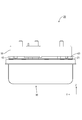
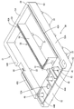
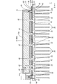
- a perspective view showing a circuit composition object of Embodiment 1 Plan view showing the circuit structure Front view showing the circuit structure Side view showing the circuit structure AA sectional view of FIG. The perspective view which shows the flame
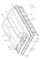
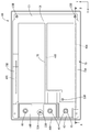
- Plan view showing the circuit structure BB sectional view of FIG. A perspective view showing a frame in which a bus bar and a synthetic resin are integrated by insert molding
- the electrical junction box 10 is arranged in a power supply path between a power source such as a battery of a vehicle such as an electric vehicle or a hybrid vehicle and a load including an in-vehicle electrical component such as a lamp or a motor, for example, a DC-DC converter, It can be used for an inverter or the like.
- a power source such as a battery of a vehicle such as an electric vehicle or a hybrid vehicle
- a load including an in-vehicle electrical component such as a lamp or a motor, for example, a DC-DC converter, It can be used for an inverter or the like.
- a power source such as a battery of a vehicle such as an electric vehicle or a hybrid vehicle
- a load including an in-vehicle electrical component such as a lamp or a motor, for example, a DC-DC converter, It can be used for an inverter or the like.
- the X direction in FIG. 1 is the front
- the Y direction is the left
- the electrical junction box 10 includes a circuit configuration body 20 and a cover 11 that covers the circuit configuration body 20.
- the cover 11 is made of a synthetic resin or metal and has a box shape with the lower part opened.
- the circuit structure 20 includes a substrate 21, a heat radiating member 30 that is stacked under the substrate 21, and dissipates heat of the substrate 21 to the outside, and a plate with respect to the surface of the substrate 21.
- a plurality of bus bars 40A to 40C that stand up above the substrate 21 in a direction in which the planes are orthogonal (cross directions), and a frame 50 that holds the bus bars 40A to 40C.
- the substrate 21 is a rectangular printed circuit board in which a conductive path made of a copper foil or the like is printed on an insulating plate made of an insulating material, and a plurality of through holes through which the terminal portions 43 of the bus bars 40A to 40C are inserted.
- substrate 21 is piled up on the whole surface except the edge part of the upper surface of the thermal radiation member 30, and the some electronic component which is not shown in figure is mounted.
- the plurality of electronic components include FETs (Field Effect Transistors), coils, capacitors, resistors, and the like.
- the heat radiating member 30 is made of a metal material having high thermal conductivity such as aluminum, aluminum alloy, copper, copper alloy, and the like, and is arranged below the plate-like portion 31 and a plate-like plate-like portion 31 on which the substrate 21 is placed. And a plurality of heat dissipating fins 35 provided.
- a flat flat surface 31 A On the upper surface of the plate-like portion 31, a flat flat surface 31 A, a relief recess 32 that escapes so as not to contact the connection portion 42 of the bus bars 40 A to 40 C and the head of the screw 67, and a screw 68 with respect to the substrate 21.
- a screw hole 33 that can be screwed is formed.
- bus bars 40A-40C are both plate-shaped, and are made of, for example, a metal such as copper, copper alloy, aluminum, or aluminum alloy, and are formed by punching a metal plate material according to the shape of the conductive path.
- Each of the bus bars 40A to 40C includes a main body 41 extending in a strip shape in the longitudinal direction and a plurality of connection portions 42 protruding from one side edge portion of the main body 41 at intervals in the longitudinal direction.
- the main body 41 extends in the longitudinal direction with a constant width dimension.
- the connection portion 42 is configured to penetrate the through hole 22 of the substrate 21 in a state where the frame 50 to which the bus bars 40A to 40C are fixed is placed on the substrate 21.
- the bus bar 40A includes a terminal portion 43 connected to an external terminal.
- the terminal portion 43 has a rectangular plate shape, is connected to an end portion of the main body 41 of the bus bar 40 ⁇ / b> A, is bent, and extends in a direction perpendicular to the plate surface of the main body 41.
- terminal portions 44 ⁇ / b> A and 44 ⁇ / b> B are arranged side by side on the side of the terminal portion 43.
- Bolt holes 45 are formed through the central portions of the terminal portions 43, 44A and 44B.
- the shaft portion of the stud bolt 46 is inserted into the bolt hole 45, and the head portion of the stud bolt 46 is fixed to the lower surface (back surface) of the terminal portions 43, 44A, and 44B by welding or the like, for example.
- the frame 50 is made of an insulating synthetic resin.
- engineering plastics heat resistance of 100 ° C. or higher, strength of 50 MPa or higher, bending elastic modulus of 2.4 GPa or higher
- a resin with high heat dissipation is used.
- the frame 50 includes a rectangular outer frame portion 51 disposed along the edge portion of the upper surface of the heat dissipation member 30 and an inner frame portion 56 extending so as to connect the inside of the outer frame portion 51.
- the outer frame portion 51 includes a pedestal portion 52 on which the terminal portions 43, 44 ⁇ / b> A, and 44 ⁇ / b> B are placed, a pair of left and right bus bar fixing frames 53 ⁇ / b> A and 53 ⁇ / b> B provided at a position continuous to the rear of the pedestal portion 52, And a connecting frame 54 that connects the rear ends of the frames 53A and 53B.
- the pedestal portion 52 is disposed between the terminal portions 43, 44 ⁇ / b> A, 44 ⁇ / b> B and the substrate 21 to hold the positions of the terminal portions 43, 44 ⁇ / b> A, 44 ⁇ / b> B with respect to the substrate 21 and accommodates the head of the stud bolt 46.
- a receiving portion (not shown) is recessed in the center of the mounting surface of the terminal portions 43, 44A, 44B.
- the pedestal portion 52 is formed with an insertion hole 52A and a partition wall 52B that insulates between the terminal portions 43 and 44A.
- the insertion hole 52A penetrates the pedestal portion 52 up and down, and a tool for screwing the substrate 21 to the heat dissipation member 30 can be inserted.
- the pair of bus bar fixing frames 53A and 53B and the inner frame portion 56 are strips having a large thickness in the vertical direction (a direction in which the substrate 21 and the frame 50 overlap) and a small thickness in the left and right direction, and the bus bars 40A to 40C.
- a groove-like press-fitting hole 58 into which is inserted is extended in the longitudinal direction.
- the press-fit hole 58 is formed with a plurality of insertion holes 58 ⁇ / b> A through which the connection part 42 is inserted into the groove bottom 58 ⁇ / b> B at the lower end.
- the pair of groove walls (the left and right groove walls disposed opposite to each other) of the press-fitting hole 58 are in close contact with both surfaces of the bus bars 40A to 40C over the entire length in the extending direction of the bus bars 40A to 40C.
- the inner frame portion 56 includes an inner frame main body 60 having a press-fit hole 58 into which the bus bars 40A to 40C are press-fitted and bent in an L shape, and a connecting portion 61 connected to the pedestal portion 52.
- a plurality of placement portions 63 to be placed on the substrate 21 are formed at the positions of the four corners.
- the plurality of placement portions 63 are cylindrical and project downward (on the substrate 21 side).
- the shape of the mounting portion 63 is not limited to a cylindrical shape, and may be, for example, a prismatic shape or a long shape extending along the direction in which the outer frame portion 51 extends. As shown in FIG.
- a fastening portion 64 that can be screwed with a screw 67 from below is formed on the lower surface (back surface) of the mounting portion 63.
- the fastening portion 64 is formed with a screw hole to which the shaft portion of the screw 67 that passes through the screw hole 23B of the substrate 21 is screwed.
- the assembly of the electrical junction box 10 will be described.
- the bus bars 40A to 40C are press-fitted into the press-fitting holes 58 of the frame 50. Note that an adhesive may be applied after the press-fitting of the bus bars 40A to 40C.
- the frame 50 into which the bus bars 40A to 40C are press-fitted is placed on the substrate 21, and the substrate 21 is screwed to the fastening portion 64 of the frame 50 with screws 67.
- the plurality of connection portions 42 inserted through the through holes 22 are soldered to the conductive paths of the substrate 21 by flow soldering.
- the heat dissipating member 30 is stacked under the substrate 21 and screwed to the heat dissipating member 30 through the screw 68 in the screw hole 23B of the substrate 21, thereby forming the circuit structure 20 (FIG. 1).
- An insulating layer may be formed between the substrate 21 and the heat dissipation member 30 with an adhesive or the like.
- the circuit configuration body 20 includes a board 21 having a conductive path and a connection portion 42 connected to the conductive path of the board 21, and is a plate-like shape arranged in a direction in which the plate surface intersects the surface of the board 21.
- the bus bars 40A to 40C are stacked on the opposite side of the substrate 21 from the bus bars 40A to 40C, and extend along the bus bars 40A to 40C.
- a synthetic resin frame 50 that holds the bus bars 40A to 40C in close contact with each other, and the frame 50 has a mounting portion 63 mounted on the substrate 21 (at least one of the substrate 21 and the heat dissipation member 30).
- the bus bars 40A to 40C are held by the frame 50, and the frame 50 has the mounting portion 63 mounted on the substrate 21, so that stress due to vibration of the vehicle or the like causes the connection portion of the bus bars 40A to 40C. It becomes difficult to reach 42. As a result, it is possible to suppress a decrease in connection reliability at the connection portion between the conductive path of the substrate 21 and the bus bars 40A to 40C. Further, since the plate surfaces of the bus bars 40A to 40C are arranged in a direction perpendicular to (intersect with) the surface of the substrate 21, the area occupied by the bus bars 40A to 40C on the substrate 21 can be reduced.
- the circuit structure 20 can be reduced in size. Further, since the heat of the bus bars 40A to 40C can be radiated from the frame 50 to the outside, it is possible to improve the heat dissipation.
- the frame 50 has an outer frame portion 51 disposed along the edge of the heat dissipation member 30, and the bus bars 40 A to 40 C are held by the outer frame portion 51. In this way, the heat of the bus bars 40A to 40C can be radiated from the outer frame portion 51 to the outside.
- the board 21 is a printed board, and the printed board is overlaid on the heat dissipation member 30. In this way, the heat of the substrate 21 can be directly transmitted to the heat dissipation member 30 as compared with the configuration in which the bus bars 40A to 40C are arranged between the substrate 21 and the heat dissipation member 30.
- the placement portion 63 is placed on the substrate 21 and has a fastening portion 64 that is screwed to the substrate 21 with a screw 67. If it does in this way, the board
- FIG. 1 A block diagram illustrating an exemplary computing environment in accordance with the present disclosure.
- the bus bar 40A has a terminal portion 43 that can be connected to an external terminal, and the frame 50 has a pedestal portion 52 on which the terminal portion 43 is placed. If it does in this way, it will become possible to absorb the torque at the time of connecting an external terminal to terminal part 43 with frame 50.
- the terminal portion 43 has a plate surface along the surface of the substrate 21, and the pedestal portion 52 is disposed between the terminal portion 43 and the substrate 21. In this way, since the terminal portion 43 can be disposed in the region on the substrate 21, the circuit structure 20 can be reduced in size compared to the configuration in which the terminal portion 43 is disposed outside the region of the substrate 21. Can do.
- the bus bars 40A to 40C are press-fitted into the press-fitting holes 58 of the frame 50.
- the bus bars 40A to 40C and the frame 70 are formed by insert molding. It is the structure formed integrally.
- the same configurations as those of the first embodiment are denoted by the same reference numerals and description thereof is omitted.
- the frame 70 is made of an insulating synthetic resin, and as shown in FIG. 7, a rectangular outer frame portion 71 arranged along the edge of the upper surface of the heat dissipation member 30, and an inner side of the outer frame portion 71. And an inner frame portion 76 extending so as to connect the two.
- the outer frame portion 71 includes a pedestal portion 52 on which the terminal portions 43, 44 ⁇ / b> A, and 44 ⁇ / b> B are placed, a pair of left and right bus bar fixing frames 73 ⁇ / b> A and 73 ⁇ / b> B provided at a position continuous to the rear of the pedestal portion 52, and a pair of bus bar fixings. And a connecting frame 54 that connects the rear ends of the frames 73A and 73B.
- the pair of bus bar fixing frames 73A and 73B and the inner frame portion 76 are strips having a large thickness in the vertical direction and a small thickness in the horizontal direction, and as shown in FIG. 9, the bus bar fixing frames 73A and 73B and the inner frame portion.
- the main body 41 of the bus bars 40A to 40C is embedded in the inside 76, and the connection portion 42 is exposed to the outside from the lower end portions of the bus bar fixing frames 73A and 73B and the inner frame portion 76.
- the entire portions embedded in the bus bar fixing frames 73A and 73B and the inner frame portion 76 are in close contact with the synthetic resin constituting the bus bar fixing frames 73A and 73B and the inner frame portion 76.
- the mounting portion 63 of the frames 50 and 70 is configured to be mounted on the substrate 21, but is not limited thereto, and may be configured to be mounted on the upper surface of the heat dissipation member 30.
- the configuration is not limited to the configuration in which the plurality of placement portions 63 are placed on one of the substrate 21 and the heat dissipation member 30, and the plurality of placement portions 63 are placed on both the substrate 21 and the heat dissipation member 30. It may be.
- the plate surfaces of the bus bars 40A to 40C are oriented perpendicular to the surface of the substrate 21, the plate surfaces of the bus bars 40A to 40C are not limited to being orthogonal to the surface of the substrate 21. It is good also as a structure arrange
Abstract
回路構成体20は、導電路を有する基板21と、基板21の導電路に接続される接続部42を有し、基板21の面に対して板面が交差する向きで配される板状のバスバー40A~40Cと、基板21におけるバスバー40A~40C側とは反対側に重ねられ、基板21の熱を放熱する放熱部材30と、バスバー40A~40Cに沿って延び、バスバー40A~40Cに対して密着状態でバスバー40A~40Cを保持する樹脂製のフレーム50と、を備え、フレーム50は、基板21及び放熱部材30の少なくとも一方に載置される載置部63を有する。
Description
本明細書では、回路構成体及び電気接続箱に関する技術を開示する。
従来、プリント基板の導電路にバスバーを接続する技術が知られている。特許文献1の電線補助部材は、長手方向に延びる本体部の左側側部に複数のリード部が設けられており、複数のリード部がプリント基板のスルーホールに挿入されて半田付けされる。複数のリード部は、先細り形状のリード部を有し、このリード部がスルーホールに挿入されると、リード部の角部がスルーホールに内接して食い込み、電線補助部材がプリント基板に対して機械的に自立するように構成されている。また、複数のリード部の間には、リード部よりも短い複数の突起部が設けられており、複数の突起部がプリント基板に当接した状態で維持される。
ところで、特許文献1は、電線補助部材に設けられたリード部や突起部によりプリント基板に対する電線補助部材の位置を保持しているため、電線補助部材が振動を受けると、電線補助部材におけるプリント基板のスルーホールに半田付けした箇所に応力がかかり、電線補助部材とプリント基板とが半田付けにより接続された箇所の接続信頼性の低下が懸念される。
本明細書に記載された技術は、上記のような事情に基づいて完成されたものであって、
基板の導電路とバスバーとの接続部分における接続信頼性の低下を抑制することを目的とする。
基板の導電路とバスバーとの接続部分における接続信頼性の低下を抑制することを目的とする。
本明細書に記載された回路構成体は、導電路を有する基板と、前記基板の導電路に接続される接続部を有し、前記基板の面に対して板面が交差する向きで配される板状のバスバーと、前記基板における前記バスバー側とは反対側に重ねられ、前記基板の熱を放熱する放熱部材と、前記バスバーに沿って延び、前記バスバーに対して密着状態で前記バスバーを保持する樹脂製のフレームと、を備え、前記フレームは、前記基板及び前記放熱部材の少なくとも一方に載置される載置部を有する。
上記構成によれば、バスバーはフレームに保持され、フレームは基板に載置部が載置されているため、車両等の振動による応力がバスバーの接続部に及びにくくなる。これにより、基板の導電路とバスバーとの接続部分における接続信頼性の低下を抑制することが可能になる。
また、バスバーの板面は、基板の面と交差する向きで配されているため、基板上においてバスバーが占める面積を小さくすることができる。これにより、基板上における電子部品を実装可能な面積を大きくすることができるため、回路構成体を小型化することが可能になる。
また、バスバーの熱をフレームから外部に放熱することができるため、放熱性を向上させることが可能になる。
上記構成によれば、バスバーはフレームに保持され、フレームは基板に載置部が載置されているため、車両等の振動による応力がバスバーの接続部に及びにくくなる。これにより、基板の導電路とバスバーとの接続部分における接続信頼性の低下を抑制することが可能になる。
また、バスバーの板面は、基板の面と交差する向きで配されているため、基板上においてバスバーが占める面積を小さくすることができる。これにより、基板上における電子部品を実装可能な面積を大きくすることができるため、回路構成体を小型化することが可能になる。
また、バスバーの熱をフレームから外部に放熱することができるため、放熱性を向上させることが可能になる。
本明細書に記載された技術の実施態様としては以下の態様が好ましい。
前記フレームは、前記放熱部材の縁部に沿って配される外枠部を有し、前記バスバーは、前記外枠部に保持されている。
このようにすれば、バスバーの熱を外枠部から外部に放熱することができる。
前記フレームは、前記放熱部材の縁部に沿って配される外枠部を有し、前記バスバーは、前記外枠部に保持されている。
このようにすれば、バスバーの熱を外枠部から外部に放熱することができる。
前記基板は、プリント基板であり、前記プリント基板が前記放熱部材に重ねられている。
このようにすれば、プリント基板と放熱部材との間にバスバーが配される構成と比較して、プリント基板の熱を直接的に放熱部材に伝えることができる。
このようにすれば、プリント基板と放熱部材との間にバスバーが配される構成と比較して、プリント基板の熱を直接的に放熱部材に伝えることができる。
前記載置部は、前記基板に載置されるものであり、前記基板にネジでネジ留めされる留め部を有する。
このようにすれば、載置部の構成を利用して基板と放熱部材とをネジ留めすることができる。
このようにすれば、載置部の構成を利用して基板と放熱部材とをネジ留めすることができる。
前記バスバーは、外部の端子と接続可能な端子部を有し、前記フレームは、前記端子部が載置される台座部を有する。
このようにすれば、外部の端子を端子部に接続する際のトルクをフレームで吸収することが可能になる。
このようにすれば、外部の端子を端子部に接続する際のトルクをフレームで吸収することが可能になる。
前記端子部は、前記基板の面に沿う板面を有し、前記台座部は、前記端子部と前記基板との間に配されている。
このようにすれば、端子部を基板上の領域に配することができるため、端子部を基板の領域の外側に配する構成と比較して回路構成体を小型化することができる。
このようにすれば、端子部を基板上の領域に配することができるため、端子部を基板の領域の外側に配する構成と比較して回路構成体を小型化することができる。
前記回路構成体と、前記回路構成体を覆うカバーとを備える電気接続箱とする。
本明細書に記載された技術によれば、基板の導電路とバスバーとの接続部分における接続信頼性の低下を抑制することが可能になる。
<実施形態1>
実施形態1を図1~図6を参照しつつ説明する。
電気接続箱10は、例えば電気自動車やハイブリット自動車等の車両のバッテリ等の電源とランプ等の車載電装品やモータ等からなる負荷との間の電力供給経路に配され、例えばDC-DCコンバータやインバータ等に用いることができる。以下では、図1のX方向を前方、Y方向を左方、Z方向を上方として説明する。
実施形態1を図1~図6を参照しつつ説明する。
電気接続箱10は、例えば電気自動車やハイブリット自動車等の車両のバッテリ等の電源とランプ等の車載電装品やモータ等からなる負荷との間の電力供給経路に配され、例えばDC-DCコンバータやインバータ等に用いることができる。以下では、図1のX方向を前方、Y方向を左方、Z方向を上方として説明する。
(電気接続箱10)
電気接続箱10は、図5に示すように、回路構成体20と、回路構成体20を覆うカバー11とを備える。カバー11は、合成樹脂製又は金属製であって、下方が開放された箱形をなす。
電気接続箱10は、図5に示すように、回路構成体20と、回路構成体20を覆うカバー11とを備える。カバー11は、合成樹脂製又は金属製であって、下方が開放された箱形をなす。
(回路構成体20)
回路構成体20は、図1,図5に示すように、基板21と、基板21の下に重ねられ、基板21の熱を外部に放熱する放熱部材30と、基板21の面に対して板面が直交する向き(交差する向き)で基板21の上方側に起立する複数のバスバー40A~40Cと、バスバー40A~40Cを保持するフレーム50と、を備える。
回路構成体20は、図1,図5に示すように、基板21と、基板21の下に重ねられ、基板21の熱を外部に放熱する放熱部材30と、基板21の面に対して板面が直交する向き(交差する向き)で基板21の上方側に起立する複数のバスバー40A~40Cと、バスバー40A~40Cを保持するフレーム50と、を備える。
(基板21)
基板21は、長方形状であって、絶縁材料からなる絶縁板に銅箔等からなる導電路が印刷されたプリント基板とされており、バスバー40A~40Cの端子部43が挿通される複数のスルーホール22と、ネジ67でネジ留めするための複数のネジ孔23A,23Bとが貫通形成されている。基板21は、放熱部材30の上面の縁部を除いた全面に重ねられており、図示しない複数の電子部品が実装されている。複数の電子部品は、FET(Field Effect Transistor)、コイル、コンデンサ、抵抗等からなる。
基板21は、長方形状であって、絶縁材料からなる絶縁板に銅箔等からなる導電路が印刷されたプリント基板とされており、バスバー40A~40Cの端子部43が挿通される複数のスルーホール22と、ネジ67でネジ留めするための複数のネジ孔23A,23Bとが貫通形成されている。基板21は、放熱部材30の上面の縁部を除いた全面に重ねられており、図示しない複数の電子部品が実装されている。複数の電子部品は、FET(Field Effect Transistor)、コイル、コンデンサ、抵抗等からなる。
(放熱部材30)
放熱部材30は、アルミニウム、アルミニウム合金、銅、銅合金等の熱伝導性が高い金属材料からなり、基板21が載置される板状の板状部31と、板状部31の下方に並んで設けられた複数の放熱フィン35とを備える。板状部31の上面には、平坦な平坦面31Aと、バスバー40A~40Cの接続部42やネジ67の頭部に当接しないように逃がす逃がし凹部32と、基板21に対してネジ68でネジ留め可能なネジ孔33とが形成されている。
放熱部材30は、アルミニウム、アルミニウム合金、銅、銅合金等の熱伝導性が高い金属材料からなり、基板21が載置される板状の板状部31と、板状部31の下方に並んで設けられた複数の放熱フィン35とを備える。板状部31の上面には、平坦な平坦面31Aと、バスバー40A~40Cの接続部42やネジ67の頭部に当接しないように逃がす逃がし凹部32と、基板21に対してネジ68でネジ留め可能なネジ孔33とが形成されている。
(バスバー40A~40C)
バスバー40A~40Cは、共に板状であって、例えば、銅、銅合金、アルミニウム、アルミニウム合金等の金属からなり、金属板材を導電路の形状に応じて打ち抜いて形成されている。各バスバー40A~40Cは、長手方向に帯状に延びる本体41と、本体41の一方の側縁部から長手方向に互いに間隔を空けて突出する複数の接続部42とを備えている。本体41は、一定の幅寸法で長手方向に延びている。バスバー40A~40Cが固定されたフレーム50が基板21に載置された状態で、接続部42は、基板21のスルーホール22を貫通するように構成されている。
バスバー40A~40Cは、共に板状であって、例えば、銅、銅合金、アルミニウム、アルミニウム合金等の金属からなり、金属板材を導電路の形状に応じて打ち抜いて形成されている。各バスバー40A~40Cは、長手方向に帯状に延びる本体41と、本体41の一方の側縁部から長手方向に互いに間隔を空けて突出する複数の接続部42とを備えている。本体41は、一定の幅寸法で長手方向に延びている。バスバー40A~40Cが固定されたフレーム50が基板21に載置された状態で、接続部42は、基板21のスルーホール22を貫通するように構成されている。
バスバー40Aは、図1に示すように、外部の端子と接続される端子部43を備える。端子部43は、長方形の板状であって、バスバー40Aの本体41の端部に連なり、屈曲されて本体41の板面と直交する方向に延びている。また、端子部43の側方には端子部44A,44Bが並んで配されている。端子部43,44A,44Bの中心部にはボルト孔45が貫通形成されている。ボルト孔45には、スタッドボルト46の軸部が挿通され、スタッドボルト46の頭部は、例えば、溶接等により端子部43,44A,44Bの下面(裏面)に固定されている。
(フレーム50)
フレーム50は、絶縁性の合成樹脂からなり、例えばエンジニアリング・プラスチック(耐熱性100℃以上、強度50MPa以上、曲げ弾性率2.4GPa以上)を用いることができるが、放熱性の高い樹脂を用いることが好ましい。フレーム50は、放熱部材30の上面の縁部に沿って配される長方形状の外枠部51と、外枠部51の内側を連結するように延びる内枠部56とを有する。外枠部51は、端子部43,44A,44Bが載置される台座部52と、台座部52の後方に連なる位置に設けられた左右一対のバスバー固定枠53A,53Bと、一対のバスバー固定枠53A,53Bの後端部を連結する連結枠54とを有する。台座部52は、端子部43,44A,44Bと基板21との間に配されて基板21に対する端子部43,44A,44Bの位置を保持するものであり、スタッドボルト46の頭部を収容する収容部(図示しない)が端子部43,44A,44Bの載置面の中心部に凹設されている。台座部52には、挿入孔52Aと、端子部43,44A間との間を絶縁する仕切り壁52Bとが形成されている。挿入孔52Aは、台座部52を上下に貫通しており、基板21を放熱部材30にネジ留めするための工具が挿入可能とされている。
フレーム50は、絶縁性の合成樹脂からなり、例えばエンジニアリング・プラスチック(耐熱性100℃以上、強度50MPa以上、曲げ弾性率2.4GPa以上)を用いることができるが、放熱性の高い樹脂を用いることが好ましい。フレーム50は、放熱部材30の上面の縁部に沿って配される長方形状の外枠部51と、外枠部51の内側を連結するように延びる内枠部56とを有する。外枠部51は、端子部43,44A,44Bが載置される台座部52と、台座部52の後方に連なる位置に設けられた左右一対のバスバー固定枠53A,53Bと、一対のバスバー固定枠53A,53Bの後端部を連結する連結枠54とを有する。台座部52は、端子部43,44A,44Bと基板21との間に配されて基板21に対する端子部43,44A,44Bの位置を保持するものであり、スタッドボルト46の頭部を収容する収容部(図示しない)が端子部43,44A,44Bの載置面の中心部に凹設されている。台座部52には、挿入孔52Aと、端子部43,44A間との間を絶縁する仕切り壁52Bとが形成されている。挿入孔52Aは、台座部52を上下に貫通しており、基板21を放熱部材30にネジ留めするための工具が挿入可能とされている。
一対のバスバー固定枠53A,53B、及び、内枠部56は、上下方向(基板21とフレーム50とが重なる方向)の厚みが大きく、左右方向の厚みが小さい帯状であって、バスバー40A~40Cが圧入される溝状の圧入孔58が長手方向に延びている。圧入孔58は、図5に示すように、下端の溝底58Bに接続部42が挿通される複数の挿通孔58Aが貫通形成されている。圧入孔58の一対の溝壁(対向配置された左右の溝壁)は、バスバー40A~40Cの延びる方向の全長に亘ってバスバー40A~40Cの板面の両面に密着する。
内枠部56は、図6に示すように、L字状に曲がってバスバー40A~40Cが圧入される圧入孔58を有する内枠本体60と、台座部52と連結される連結部61とを有する。
外枠部51の下面(裏面)には、四隅の位置に、基板21に載置される複数の載置部63が形成されている。複数の載置部63は、円柱状であって、下方(基板21側)に突出している。なお、載置部63の形状は円柱状に限られず、例えば、角柱状としたり、外枠部51の延びる方向に沿って延びる長尺の形状としてもよい。載置部63の下面(裏面)には、図5に示すように、下方からネジ67でネジ留め可能な留め部64が形成されている。留め部64には、基板21のネジ孔23Bを通ったネジ67の軸部がネジ留めされるネジ孔が形成されている。
外枠部51の下面(裏面)には、四隅の位置に、基板21に載置される複数の載置部63が形成されている。複数の載置部63は、円柱状であって、下方(基板21側)に突出している。なお、載置部63の形状は円柱状に限られず、例えば、角柱状としたり、外枠部51の延びる方向に沿って延びる長尺の形状としてもよい。載置部63の下面(裏面)には、図5に示すように、下方からネジ67でネジ留め可能な留め部64が形成されている。留め部64には、基板21のネジ孔23Bを通ったネジ67の軸部がネジ留めされるネジ孔が形成されている。
電気接続箱10の組み付けについて説明する。
フレーム50の圧入孔58にバスバー40A~40Cを圧入する。なお、バスバー40A~40Cの圧入後に接着剤を塗布してもよい。次に、バスバー40A~40Cを圧入したフレーム50を基板21に載置し、ネジ67で基板21をフレーム50の留め部64にネジ留めする。そして、フロー半田付けにより、スルーホール22に挿通された状態の複数の接続部42を基板21の導電路に半田付けする。
フレーム50の圧入孔58にバスバー40A~40Cを圧入する。なお、バスバー40A~40Cの圧入後に接着剤を塗布してもよい。次に、バスバー40A~40Cを圧入したフレーム50を基板21に載置し、ネジ67で基板21をフレーム50の留め部64にネジ留めする。そして、フロー半田付けにより、スルーホール22に挿通された状態の複数の接続部42を基板21の導電路に半田付けする。
次に、基板21の下に放熱部材30を重ね、基板21のネジ孔23Bにネジ68を通して放熱部材30にネジ留めすることにより、回路構成体20(図1)が形成される。なお、基板21と放熱部材30との間に接着剤等により絶縁層を形成してもよい。回路構成体20にカバー11を被せると電気接続箱10が形成される(図5参照)。
本実施形態の作用、効果について説明する。
回路構成体20は、導電路を有する基板21と、基板21の導電路に接続される接続部42を有し、基板21の面に対して板面が交差する向きで配される板状のバスバー40A~40Cと、基板21におけるバスバー40A~40C側とは反対側に重ねられ、基板21の熱を放熱する放熱部材30と、バスバー40A~40Cに沿って延び、バスバー40A~40Cに対して密着状態でバスバー40A~40Cを保持する合成樹脂製のフレーム50と、を備え、フレーム50は、基板21(基板21及び放熱部材30の少なくとも一方)に載置される載置部63を有する。
回路構成体20は、導電路を有する基板21と、基板21の導電路に接続される接続部42を有し、基板21の面に対して板面が交差する向きで配される板状のバスバー40A~40Cと、基板21におけるバスバー40A~40C側とは反対側に重ねられ、基板21の熱を放熱する放熱部材30と、バスバー40A~40Cに沿って延び、バスバー40A~40Cに対して密着状態でバスバー40A~40Cを保持する合成樹脂製のフレーム50と、を備え、フレーム50は、基板21(基板21及び放熱部材30の少なくとも一方)に載置される載置部63を有する。
本実施形態によれば、バスバー40A~40Cはフレーム50に保持され、フレーム50は基板21に載置部63が載置されているため、車両等の振動による応力がバスバー40A~40Cの接続部42に及びにくくなる。これにより、基板21の導電路とバスバー40A~40Cとの接続部分における接続信頼性の低下を抑制することが可能になる。また、バスバー40A~40Cの板面は、基板21の面と直交する向き(交差する向き)で配されているため、基板21上においてバスバー40A~40Cが占める面積を小さくすることができる。これにより、基板21上における電子部品を実装可能な面積を大きくすることができるため、回路構成体20を小型化することが可能になる。また、バスバー40A~40Cの熱をフレーム50から外部に放熱することができるため、放熱性を向上させることが可能になる。
また、フレーム50は、放熱部材30の縁部に沿って配される外枠部51を有し、バスバー40A~40Cは、外枠部51に保持されている。
このようにすれば、バスバー40A~40Cの熱を外枠部51から外部に放熱することができる。
このようにすれば、バスバー40A~40Cの熱を外枠部51から外部に放熱することができる。
また、基板21は、プリント基板であり、プリント基板が放熱部材30に重ねられている。
このようにすれば、基板21と放熱部材30との間にバスバー40A~40Cが配される構成と比較して、基板21の熱を直接的に放熱部材30に伝えることができる。
このようにすれば、基板21と放熱部材30との間にバスバー40A~40Cが配される構成と比較して、基板21の熱を直接的に放熱部材30に伝えることができる。
また、載置部63は、基板21に載置されるものであり、基板21にネジ67でネジ留めされる留め部64を有する。
このようにすれば、載置部63の構成を利用して基板21と放熱部材30とをネジ留めすることができる。
このようにすれば、載置部63の構成を利用して基板21と放熱部材30とをネジ留めすることができる。
バスバー40Aは、外部の端子と接続可能な端子部43を有し、フレーム50は、端子部43が載置される台座部52を有する。
このようにすれば、外部の端子を端子部43に接続する際のトルクをフレーム50で吸収することが可能になる。
このようにすれば、外部の端子を端子部43に接続する際のトルクをフレーム50で吸収することが可能になる。
端子部43は、基板21の面に沿う板面を有し、台座部52は、端子部43と基板21との間に配されている。
このようにすれば、端子部43を基板21上の領域に配することができるため、端子部43を基板21の領域の外側に配する構成と比較して回路構成体20を小型化することができる。
このようにすれば、端子部43を基板21上の領域に配することができるため、端子部43を基板21の領域の外側に配する構成と比較して回路構成体20を小型化することができる。
<実施形態2>
次に、実施形態2を図7~図10を参照して説明する。実施形態1の回路構成体20は、フレーム50の圧入孔58にバスバー40A~40Cが圧入されていたが、実施形態2の電気接続箱69は、インサート成形によりバスバー40A~40Cとフレーム70とが一体的に形成されている構成である。以下では、他の構成は実施形態1と同一であるため、実施形態1と同一の構成については同一の符号を付して説明を省略する。
次に、実施形態2を図7~図10を参照して説明する。実施形態1の回路構成体20は、フレーム50の圧入孔58にバスバー40A~40Cが圧入されていたが、実施形態2の電気接続箱69は、インサート成形によりバスバー40A~40Cとフレーム70とが一体的に形成されている構成である。以下では、他の構成は実施形態1と同一であるため、実施形態1と同一の構成については同一の符号を付して説明を省略する。
(フレーム70)
フレーム70は、絶縁性の合成樹脂製であって、図7に示すように、放熱部材30の上面の縁部に沿って配される長方形状の外枠部71と、外枠部71の内側を連結するように延びる内枠部76とを有する。外枠部71は、端子部43,44A,44Bが載置される台座部52と、台座部52の後方に連なる位置に設けられた左右一対のバスバー固定枠73A,73Bと、一対のバスバー固定枠73A,73Bの後端部を連結する連結枠54とを有する。
フレーム70は、絶縁性の合成樹脂製であって、図7に示すように、放熱部材30の上面の縁部に沿って配される長方形状の外枠部71と、外枠部71の内側を連結するように延びる内枠部76とを有する。外枠部71は、端子部43,44A,44Bが載置される台座部52と、台座部52の後方に連なる位置に設けられた左右一対のバスバー固定枠73A,73Bと、一対のバスバー固定枠73A,73Bの後端部を連結する連結枠54とを有する。
一対のバスバー固定枠73A,73B及び内枠部76は、上下方向の厚みが大きく、左右方向の厚みが小さい帯状であって、図9に示すように、バスバー固定枠73A,73B及び内枠部76の内部にバスバー40A~40Cの本体41が埋設されており、バスバー固定枠73A,73B及び内枠部76の下端部から接続部42が外部に露出している。バスバー40A~40Cのうち、バスバー固定枠73A,73B及び内枠部76に埋設された部分の全体は、バスバー固定枠73A,73B及び内枠部76を構成する合成樹脂に密着している。
<他の実施形態>
本明細書に記載された技術は上記記述及び図面によって説明した実施形態に限定されるものではなく、例えば次のような実施形態も本明細書に記載された技術の技術的範囲に含まれる。
本明細書に記載された技術は上記記述及び図面によって説明した実施形態に限定されるものではなく、例えば次のような実施形態も本明細書に記載された技術の技術的範囲に含まれる。
(1)上記実施形態では、フレーム50,70の載置部63は、基板21に載置される構成としたが、これに限られず、放熱部材30の上面に載置される構成としてもよい。また、複数の載置部63が基板21及び放熱部材30の一方に載置される構成に限られず、複数の載置部63が基板21と放熱部材30の双方に対して載置されるようにしてもよい。
(2)バスバー40A~40Cの板面は、基板21の面と直交する向きとしたが、これに限られず、バスバー40A~40Cの板面は、基板21の面に対して直交以外の角度で交差する向きに配置される構成としてもよい。
10: 電気接続箱
11: カバー
20,69: 回路構成体
21: 基板
22: スルーホール
23: ネジ孔
30: 放熱部材
40A~40C: バスバー
42: 接続部
43,44A,44B: 端子部
50,70: フレーム
51,71: 外枠部
52: 台座部
63: 載置部
11: カバー
20,69: 回路構成体
21: 基板
22: スルーホール
23: ネジ孔
30: 放熱部材
40A~40C: バスバー
42: 接続部
43,44A,44B: 端子部
50,70: フレーム
51,71: 外枠部
52: 台座部
63: 載置部
Claims (7)
- 導電路を有する基板と、
前記基板の導電路に接続される接続部を有し、前記基板の面に対して板面が交差する向きで配される板状のバスバーと、
前記基板における前記バスバー側とは反対側に重ねられ、前記基板の熱を放熱する放熱部材と、
前記バスバーに沿って延び、前記バスバーに対して密着状態で前記バスバーを保持する樹脂製のフレームと、を備え、
前記フレームは、前記基板及び前記放熱部材の少なくとも一方に載置される載置部を有する回路構成体。 - 前記フレームは、前記放熱部材の縁部に沿って配される外枠部を有し、
前記バスバーは、前記外枠部に保持されている請求項1に記載の回路構成体。 - 前記基板は、プリント基板であり、
前記プリント基板が前記放熱部材に重ねられている請求項1又は請求項2に記載の回路構成体。 - 前記載置部は、前記基板に載置されるものであり、前記基板にネジでネジ留めされる留め部を有する請求項1から請求項3のいずれか一項に記載の回路構成体。
- 前記バスバーは、外部の端子と接続可能な端子部を有し、
前記フレームは、前記端子部が載置される台座部を有する請求項1から請求項4のいずれか一項に記載の回路構成体。 - 前記端子部は、前記基板の面に沿う板面を有し、
前記台座部は、前記端子部と前記基板との間に配されている請求項5に記載の回路構成体。 - 請求項1から請求項6のいずれか一項に記載の回路構成体と、前記回路構成体を覆うカバーとを備える電気接続箱。
Priority Applications (4)
| Application Number | Priority Date | Filing Date | Title |
|---|---|---|---|
| CN201880027498.7A CN110915312B (zh) | 2017-05-11 | 2018-04-25 | 电路结构体及电气连接箱 |
| DE112018002422.9T DE112018002422T5 (de) | 2017-05-11 | 2018-04-25 | Schaltungsanordnung und elektrischer Verteilerkasten |
| KR1020197032491A KR102287797B1 (ko) | 2017-05-11 | 2018-04-25 | 회로 구성체 및 전기 접속 박스 |
| US16/611,522 US10893611B2 (en) | 2017-05-11 | 2018-04-25 | Circuit assembly and electrical junction box |
Applications Claiming Priority (2)
| Application Number | Priority Date | Filing Date | Title |
|---|---|---|---|
| JP2017-094551 | 2017-05-11 | ||
| JP2017094551A JP2018190914A (ja) | 2017-05-11 | 2017-05-11 | 回路構成体及び電気接続箱 |
Publications (1)
| Publication Number | Publication Date |
|---|---|
| WO2018207621A1 true WO2018207621A1 (ja) | 2018-11-15 |
Family
ID=64104499
Family Applications (1)
| Application Number | Title | Priority Date | Filing Date |
|---|---|---|---|
| PCT/JP2018/016717 WO2018207621A1 (ja) | 2017-05-11 | 2018-04-25 | 回路構成体及び電気接続箱 |
Country Status (6)
| Country | Link |
|---|---|
| US (1) | US10893611B2 (ja) |
| JP (1) | JP2018190914A (ja) |
| KR (1) | KR102287797B1 (ja) |
| CN (1) | CN110915312B (ja) |
| DE (1) | DE112018002422T5 (ja) |
| WO (1) | WO2018207621A1 (ja) |
Families Citing this family (8)
| Publication number | Priority date | Publication date | Assignee | Title |
|---|---|---|---|---|
| JP6919599B2 (ja) * | 2018-03-05 | 2021-08-18 | 住友電装株式会社 | 電気接続箱 |
| JP7426861B2 (ja) | 2020-03-17 | 2024-02-02 | 古河電気工業株式会社 | 電気接続箱及びホルダ付きバスバー |
| JP2022161400A (ja) * | 2021-04-09 | 2022-10-21 | 住友電装株式会社 | 電気接続箱 |
| JP2022161402A (ja) * | 2021-04-09 | 2022-10-21 | 住友電装株式会社 | 電気接続箱 |
| JP2022161398A (ja) * | 2021-04-09 | 2022-10-21 | 住友電装株式会社 | 電気接続箱 |
| JP2022161399A (ja) * | 2021-04-09 | 2022-10-21 | 住友電装株式会社 | 電気接続箱 |
| JP2022161401A (ja) * | 2021-04-09 | 2022-10-21 | 住友電装株式会社 | 電気接続箱 |
| JP2022161397A (ja) * | 2021-04-09 | 2022-10-21 | 住友電装株式会社 | 電気接続箱 |
Citations (6)
| Publication number | Priority date | Publication date | Assignee | Title |
|---|---|---|---|---|
| JPS52134066U (ja) * | 1976-04-06 | 1977-10-12 | ||
| JPH1141749A (ja) * | 1997-07-17 | 1999-02-12 | Yazaki Corp | バスバー固定構造 |
| JP2000003740A (ja) * | 1998-06-16 | 2000-01-07 | Yazaki Corp | 電子ユニットの配索構造 |
| JP2008125190A (ja) * | 2006-11-09 | 2008-05-29 | Auto Network Gijutsu Kenkyusho:Kk | 電気接続箱 |
| JP2014011929A (ja) * | 2012-07-03 | 2014-01-20 | Yazaki Corp | 電気接続箱 |
| JP2016184990A (ja) * | 2015-03-25 | 2016-10-20 | 株式会社タムラ製作所 | 端子ユニット及びリアクトル |
Family Cites Families (9)
| Publication number | Priority date | Publication date | Assignee | Title |
|---|---|---|---|---|
| JPH0515035A (ja) * | 1991-07-04 | 1993-01-22 | Fujikura Ltd | 電気接続箱 |
| JP3917473B2 (ja) * | 2002-06-21 | 2007-05-23 | 株式会社オートネットワーク技術研究所 | パワーモジュール |
| JP2009131017A (ja) * | 2007-11-22 | 2009-06-11 | Yaskawa Electric Corp | ブスバーサポートとそれを用いたモータ制御装置 |
| JP4974173B2 (ja) * | 2007-12-28 | 2012-07-11 | 古河電気工業株式会社 | 電気接続箱 |
| JP5679959B2 (ja) | 2011-12-27 | 2015-03-04 | 三菱電機株式会社 | 電流補助部材を用いた電流補助アセンブリ |
| JP5975070B2 (ja) * | 2014-07-16 | 2016-08-23 | 株式会社オートネットワーク技術研究所 | 電気接続箱 |
| JP6252871B2 (ja) * | 2015-01-16 | 2017-12-27 | 株式会社オートネットワーク技術研究所 | 回路構成体及び電気接続箱 |
| JP6614451B2 (ja) * | 2016-06-08 | 2019-12-04 | 株式会社オートネットワーク技術研究所 | 基板ユニット |
| US10368465B2 (en) * | 2017-09-07 | 2019-07-30 | Lear Corporation | Electrical unit |
-
2017
- 2017-05-11 JP JP2017094551A patent/JP2018190914A/ja active Pending
-
2018
- 2018-04-25 DE DE112018002422.9T patent/DE112018002422T5/de active Granted
- 2018-04-25 US US16/611,522 patent/US10893611B2/en active Active
- 2018-04-25 CN CN201880027498.7A patent/CN110915312B/zh active Active
- 2018-04-25 KR KR1020197032491A patent/KR102287797B1/ko active IP Right Grant
- 2018-04-25 WO PCT/JP2018/016717 patent/WO2018207621A1/ja active Application Filing
Patent Citations (6)
| Publication number | Priority date | Publication date | Assignee | Title |
|---|---|---|---|---|
| JPS52134066U (ja) * | 1976-04-06 | 1977-10-12 | ||
| JPH1141749A (ja) * | 1997-07-17 | 1999-02-12 | Yazaki Corp | バスバー固定構造 |
| JP2000003740A (ja) * | 1998-06-16 | 2000-01-07 | Yazaki Corp | 電子ユニットの配索構造 |
| JP2008125190A (ja) * | 2006-11-09 | 2008-05-29 | Auto Network Gijutsu Kenkyusho:Kk | 電気接続箱 |
| JP2014011929A (ja) * | 2012-07-03 | 2014-01-20 | Yazaki Corp | 電気接続箱 |
| JP2016184990A (ja) * | 2015-03-25 | 2016-10-20 | 株式会社タムラ製作所 | 端子ユニット及びリアクトル |
Also Published As
| Publication number | Publication date |
|---|---|
| US20200120803A1 (en) | 2020-04-16 |
| JP2018190914A (ja) | 2018-11-29 |
| KR102287797B1 (ko) | 2021-08-06 |
| CN110915312A (zh) | 2020-03-24 |
| CN110915312B (zh) | 2021-03-26 |
| DE112018002422T5 (de) | 2020-01-23 |
| KR20190135514A (ko) | 2019-12-06 |
| US10893611B2 (en) | 2021-01-12 |
Similar Documents
| Publication | Publication Date | Title |
|---|---|---|
| WO2018207621A1 (ja) | 回路構成体及び電気接続箱 | |
| US10194523B2 (en) | Circuit assembly, electrical junction box, and manufacturing method for circuit assembly | |
| JP6981564B2 (ja) | 金属部材付き基板、回路構成体及び電気接続箱 | |
| JP6958164B2 (ja) | コイル装置、基板付きコイル装置及び電気接続箱 | |
| WO2016002748A1 (ja) | 電気接続箱 | |
| JPWO2017154696A1 (ja) | 回路構成体 | |
| JP6432792B2 (ja) | 回路構成体及び電気接続箱 | |
| JP2016152349A (ja) | 回路構成体 | |
| US10448497B2 (en) | Circuit assembly and electrical junction box | |
| WO2017199837A1 (ja) | 回路構成体 | |
| WO2017098703A1 (ja) | 発熱電子部品の放熱装置、およびその製造方法、並びに車載充電器 | |
| WO2019116880A1 (ja) | 回路構成体及び電気接続箱 | |
| JP2020047765A (ja) | 電気機器及び放熱器 | |
| JP2009238923A (ja) | 電子機器 | |
| JP6321883B2 (ja) | 電子部品ユニット及び熱伝導載置部材 | |
| JP7026865B1 (ja) | パワーモジュール | |
| JP5448072B2 (ja) | 電装品取付構造 | |
| JPH0810230Y2 (ja) | 電気部品と放熱体の取付構造 | |
| JP6895065B2 (ja) | 電子部品実装体および電源装置 | |
| WO2019216366A1 (ja) | 回路構成体 | |
| JP2018018880A (ja) | 半導体素子取付基板 | |
| WO2018216466A1 (ja) | コイル装置、基板付きコイル装置及び電気接続箱 | |
| JP2022101129A (ja) | 電気接続箱 | |
| JPH08306834A (ja) | 放熱板及びその放熱板を用いた電子部品の実装構造 | |
| JPH0638468Y2 (ja) | 電子部品の放熱器 |
Legal Events
| Date | Code | Title | Description |
|---|---|---|---|
| 121 | Ep: the epo has been informed by wipo that ep was designated in this application |
Ref document number: 18798727 Country of ref document: EP Kind code of ref document: A1 |
|
| ENP | Entry into the national phase |
Ref document number: 20197032491 Country of ref document: KR Kind code of ref document: A |
|
| 122 | Ep: pct application non-entry in european phase |
Ref document number: 18798727 Country of ref document: EP Kind code of ref document: A1 |