WO2018159190A1 - 検査システム、および検査システムの故障解析・予知方法 - Google Patents
検査システム、および検査システムの故障解析・予知方法 Download PDFInfo
- Publication number
- WO2018159190A1 WO2018159190A1 PCT/JP2018/002934 JP2018002934W WO2018159190A1 WO 2018159190 A1 WO2018159190 A1 WO 2018159190A1 JP 2018002934 W JP2018002934 W JP 2018002934W WO 2018159190 A1 WO2018159190 A1 WO 2018159190A1
- Authority
- WO
- WIPO (PCT)
- Prior art keywords
- failure
- inspection
- inspection system
- tester
- location
- Prior art date
Links
Images


Classifications
-
- G—PHYSICS
- G01—MEASURING; TESTING
- G01R—MEASURING ELECTRIC VARIABLES; MEASURING MAGNETIC VARIABLES
- G01R31/00—Arrangements for testing electric properties; Arrangements for locating electric faults; Arrangements for electrical testing characterised by what is being tested not provided for elsewhere
- G01R31/28—Testing of electronic circuits, e.g. by signal tracer
- G01R31/317—Testing of digital circuits
- G01R31/31718—Logistic aspects, e.g. binning, selection, sorting of devices under test, tester/handler interaction networks, Test management software, e.g. software for test statistics or test evaluation, yield analysis
-
- G—PHYSICS
- G01—MEASURING; TESTING
- G01R—MEASURING ELECTRIC VARIABLES; MEASURING MAGNETIC VARIABLES
- G01R35/00—Testing or calibrating of apparatus covered by the other groups of this subclass
-
- G—PHYSICS
- G01—MEASURING; TESTING
- G01R—MEASURING ELECTRIC VARIABLES; MEASURING MAGNETIC VARIABLES
- G01R31/00—Arrangements for testing electric properties; Arrangements for locating electric faults; Arrangements for electrical testing characterised by what is being tested not provided for elsewhere
- G01R31/28—Testing of electronic circuits, e.g. by signal tracer
- G01R31/2851—Testing of integrated circuits [IC]
- G01R31/2886—Features relating to contacting the IC under test, e.g. probe heads; chucks
- G01R31/2891—Features relating to contacting the IC under test, e.g. probe heads; chucks related to sensing or controlling of force, position, temperature
-
- G—PHYSICS
- G01—MEASURING; TESTING
- G01R—MEASURING ELECTRIC VARIABLES; MEASURING MAGNETIC VARIABLES
- G01R1/00—Details of instruments or arrangements of the types included in groups G01R5/00 - G01R13/00 and G01R31/00
- G01R1/02—General constructional details
- G01R1/06—Measuring leads; Measuring probes
- G01R1/067—Measuring probes
- G01R1/073—Multiple probes
- G01R1/07307—Multiple probes with individual probe elements, e.g. needles, cantilever beams or bump contacts, fixed in relation to each other, e.g. bed of nails fixture or probe card
-
- G—PHYSICS
- G01—MEASURING; TESTING
- G01R—MEASURING ELECTRIC VARIABLES; MEASURING MAGNETIC VARIABLES
- G01R31/00—Arrangements for testing electric properties; Arrangements for locating electric faults; Arrangements for electrical testing characterised by what is being tested not provided for elsewhere
- G01R31/26—Testing of individual semiconductor devices
-
- G—PHYSICS
- G01—MEASURING; TESTING
- G01R—MEASURING ELECTRIC VARIABLES; MEASURING MAGNETIC VARIABLES
- G01R31/00—Arrangements for testing electric properties; Arrangements for locating electric faults; Arrangements for electrical testing characterised by what is being tested not provided for elsewhere
- G01R31/28—Testing of electronic circuits, e.g. by signal tracer
- G01R31/2851—Testing of integrated circuits [IC]
-
- G—PHYSICS
- G05—CONTROLLING; REGULATING
- G05B—CONTROL OR REGULATING SYSTEMS IN GENERAL; FUNCTIONAL ELEMENTS OF SUCH SYSTEMS; MONITORING OR TESTING ARRANGEMENTS FOR SUCH SYSTEMS OR ELEMENTS
- G05B23/00—Testing or monitoring of control systems or parts thereof
- G05B23/02—Electric testing or monitoring
- G05B23/0205—Electric testing or monitoring by means of a monitoring system capable of detecting and responding to faults
- G05B23/0259—Electric testing or monitoring by means of a monitoring system capable of detecting and responding to faults characterized by the response to fault detection
- G05B23/0283—Predictive maintenance, e.g. involving the monitoring of a system and, based on the monitoring results, taking decisions on the maintenance schedule of the monitored system; Estimating remaining useful life [RUL]
-
- H—ELECTRICITY
- H01—ELECTRIC ELEMENTS
- H01L—SEMICONDUCTOR DEVICES NOT COVERED BY CLASS H10
- H01L21/00—Processes or apparatus adapted for the manufacture or treatment of semiconductor or solid state devices or of parts thereof
- H01L21/67—Apparatus specially adapted for handling semiconductor or electric solid state devices during manufacture or treatment thereof; Apparatus specially adapted for handling wafers during manufacture or treatment of semiconductor or electric solid state devices or components ; Apparatus not specifically provided for elsewhere
- H01L21/67005—Apparatus not specifically provided for elsewhere
- H01L21/67242—Apparatus for monitoring, sorting or marking
- H01L21/67288—Monitoring of warpage, curvature, damage, defects or the like
-
- H—ELECTRICITY
- H01—ELECTRIC ELEMENTS
- H01L—SEMICONDUCTOR DEVICES NOT COVERED BY CLASS H10
- H01L22/00—Testing or measuring during manufacture or treatment; Reliability measurements, i.e. testing of parts without further processing to modify the parts as such; Structural arrangements therefor
- H01L22/10—Measuring as part of the manufacturing process
- H01L22/14—Measuring as part of the manufacturing process for electrical parameters, e.g. resistance, deep-levels, CV, diffusions by electrical means
-
- H—ELECTRICITY
- H01—ELECTRIC ELEMENTS
- H01L—SEMICONDUCTOR DEVICES NOT COVERED BY CLASS H10
- H01L22/00—Testing or measuring during manufacture or treatment; Reliability measurements, i.e. testing of parts without further processing to modify the parts as such; Structural arrangements therefor
- H01L22/20—Sequence of activities consisting of a plurality of measurements, corrections, marking or sorting steps
-
- H—ELECTRICITY
- H01—ELECTRIC ELEMENTS
- H01L—SEMICONDUCTOR DEVICES NOT COVERED BY CLASS H10
- H01L22/00—Testing or measuring during manufacture or treatment; Reliability measurements, i.e. testing of parts without further processing to modify the parts as such; Structural arrangements therefor
- H01L22/30—Structural arrangements specially adapted for testing or measuring during manufacture or treatment, or specially adapted for reliability measurements
-
- G—PHYSICS
- G01—MEASURING; TESTING
- G01R—MEASURING ELECTRIC VARIABLES; MEASURING MAGNETIC VARIABLES
- G01R31/00—Arrangements for testing electric properties; Arrangements for locating electric faults; Arrangements for electrical testing characterised by what is being tested not provided for elsewhere
- G01R31/28—Testing of electronic circuits, e.g. by signal tracer
- G01R31/282—Testing of electronic circuits specially adapted for particular applications not provided for elsewhere
- G01R31/2831—Testing of materials or semi-finished products, e.g. semiconductor wafers or substrates
Definitions
- the present invention relates to an inspection system for inspecting an object to be inspected, and a failure analysis / prediction method of the inspection system.
- an inspection system that performs such an electrical inspection includes a wafer stage and a wafer transfer system, a prober having a probe card having a probe that contacts a device formed on the wafer, and an electrical device connected to the device. And a tester for providing various signals and inspecting various electrical characteristics of the device.
- Patent Document 1 describes a technique for specifying a failure factor in a prober by providing a prober controller with a self-diagnosis execution function.
- the tester and the prober are manufactured by different manufacturers, and are often integrated after delivery to the customer. Even when the diagnostic function is provided, the diagnostic function is provided separately for the tester and the prober.
- the prober's diagnosis may be FAIL (NG) due to the tester or vice versa.
- FAIL FAIL
- the tester and prober Even if it has a diagnostic function, it is difficult to grasp the fault location.
- FAIL FAIL
- an object of the present invention is to provide a technique capable of quickly grasping or predicting the location even when a failure of a factor straddling a tester and a prober or a sign of the previous stage occurs.
- a stage that holds a substrate on which a plurality of devices are formed, a transport unit that transports the substrate to the stage, and a plurality of probes that contact electrodes of the plurality of devices on the substrate.
- a prober having a probe card, a tester that provides an electrical signal to a plurality of devices on the substrate via the probe card, and inspects the electrical characteristics of the device, and when a failure occurs during the inspection, Or a failure analysis / prediction processing unit that identifies or estimates or predicts the location of a failure by analyzing the history information of the prober and the tester related to the failure when an indication of the previous stage of the failure occurs.
- a stage that holds a substrate on which a plurality of devices are formed, a transport unit that transports the substrate to the stage, and a plurality of probes that contact electrodes of the plurality of devices on the substrate.
- a failure analysis / prediction method that estimates or predicts, when a failure occurs during inspection, or when a sign of the previous stage of the failure occurs, the history of the prober and the tester related to the failure
- the cause of the failure can be specified based on the knowledge of the expert, and thereby the location of the failure can be specified, estimated, or predicted.
- the tester includes a motherboard and a plurality of inspection circuit boards mounted on the motherboard, and a contact member that connects them is disposed between the probe card mounted on the prober and the motherboard, It is possible to identify, estimate, or predict the location of a failure that has occurred in any of the inspection circuit board, the motherboard, the contact member, and the probe card.
- a plurality of factors including a prober side factor and a tester side factor related thereto
- the factors that are known to be normal, or the factors that are known to be normal by obtaining a normal result as a result of performing a predetermined diagnosis are excluded and remain
- the failure location can be identified, estimated or predicted from the factors.
- the output results of inspection items that became PASS at the time of inspection can be divided into a plurality of levels, and a sign of failure can be grasped from a change in level based on a plurality of measurement results, so that the failure can be predicted.
- the output result is divided into a plurality of levels for the items that became PASS at the time of inspection, and from the distribution chart of the level of the device determined to be PASS
- the failure location can be predicted.
- a failure location can be predicted by associating the distribution map of the level of the map with the distribution of the height of the stage of the inspection object of the prober.
- the cause of the abnormality is identified based on the history information of both the prober and the tester, so that the failure location can be identified or estimated quickly.
- the failure location can be predicted before failure, so that the target part can be replaced or repaired in advance. For this reason, the operation rate of an inspection system can be improved.
- FIG. 1 It is a figure showing typically the schematic structure of the inspection system concerning one embodiment of the present invention. It is a figure for demonstrating the failure analysis / prediction process part of the inspection system of FIG. It is a figure for demonstrating the structure from the test circuit board of a tester to a wafer. It is a flowchart of a failure analysis and prediction program. It is a figure which shows a state in case the installation of the probe card 25 is not normal. It is a figure which shows the state which is diagnosing with the probe card for diagnosis. It is a figure which shows the example which set the level of OK (PASS) with respect to the inspection item in multiple steps.
- PASS level of OK
- FIG. 1 is a diagram schematically showing a schematic configuration of an inspection system according to an embodiment of the present invention.
- the inspection system performs an electrical inspection of a plurality of devices (IC chips; also referred to as DUT (Device Under Test) hereinafter) formed on the wafer at the stage where all processes on the wafer are completed.
- DUT Device Under Test
- an inspection system 100 includes a prober 200 that makes a probe of a probe card contact a device on a wafer, a tester 300 that performs an electrical inspection by giving an electrical signal to the device, a failure analysis / It has a prediction processing unit 400 and a host control unit 500.
- the prober 200 includes a main body unit 21, a transport unit 22, and a prober control unit 27.
- the main body 21 is attached to a housing 23, a head plate 24 that forms the top surface of the housing 23, a circular hole 24a is formed in the center, and a position corresponding to the hole 24a of the head plate 24.
- a probe card 25 having a probe (contactor) 25a, and a stage (wafer chuck top) 26 on which the wafer W is placed and adsorbed at a position below the probe card 25.
- the stage 26 is movable in the X, Y, Z, and ⁇ directions by an XY table mechanism, a Z direction moving mechanism, and a ⁇ direction moving mechanism (all not shown), and the wafer W is moved to a predetermined inspection position. It is designed to be positioned. Then, by raising the wafer W, the probes 25a of the probe card 25 come into contact with the electrodes of a plurality of devices.
- the transfer unit 22 includes a transfer device (not shown), and a wafer carrier and a probe card stocker (both not shown) are mounted.
- the transfer device transfers the wafer W from the wafer carrier onto the stage 26.
- the probe card 25 is conveyed below the head plate 24 from the probe card stocker.
- the prober control unit 27 controls each component of the prober 200, a main control unit having a CPU, an input unit such as a keyboard, a mouse, and a remote controller, an output unit such as a printer, a display unit such as a display, and a control And a storage unit for storing necessary information.
- the main control unit sets a storage medium in which the processing recipe is stored in the storage unit, thereby causing the prober 200 to execute a predetermined processing operation based on the processing recipe called from the storage medium.
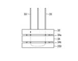
- the tester 300 includes a housing 31, a mother board 32 provided horizontally at the bottom of the housing 31, a plurality of test circuit boards 33 mounted in a standing state in slots of the mother board 32, a mother board 32, and a probe card. And a tester control unit 35.
- the mother board 32 is connected to the probe card 25 via the contact block 34.
- the contact block 34 performs connection with the mother board 32 and connection with the probe card 25 via a plurality of contact pins 34a and 34b, respectively.
- the contact pins 34a and 34b are pogo pins.
- the inspection circuit board 33 gives an electrical signal to the device on the wafer W according to various test items.
- the tester control unit 35 controls each component of the tester 300, a main control unit having a CPU, an input unit such as a keyboard, a mouse, and a remote controller, an output unit such as a printer, a display unit such as a display, and a control And a storage unit for storing necessary information.
- the main control unit sets a storage medium in which test items and the like are stored in the storage unit, thereby causing the tester 300 to execute a predetermined operation based on the test items called from the storage medium.
- the prober control unit 27 and the tester control unit 35 are each configured to record system operation history, operator operation history, diagnosis history, and other history information for the purpose of elucidating and coping with the cause of any failure.
- a history information acquisition unit (not shown) that acquires (log data) is included, and the history information acquired by the history information acquisition unit is stored in the history information storage / management unit 40.
- the failure analysis / prediction processing unit 400 has artificial intelligence (AI), and when a failure (FAIL) or a sign of failure occurs, the failure analysis / prediction processing unit 400 performs factor analysis on the information from the prober 200 or the tester 300, When the location is not known, the history information of the tester and prober related to the failure is obtained from the history information storage / management unit 40, and the location of the failure is determined based on the information and knowledge of an expert such as a service / developer. Know (identify or estimate) or predict.
- AI artificial intelligence
- the failure analysis / prediction processing unit 400 can acquire stage coordinate information, contact weight information, probe position / tilt information, and stage temperature as prober information from the history information storage / management unit 40.
- pin leak information, pin contact resistance, and pin power supply voltage / current information can be acquired as tester information.
- the host control unit 500 includes a main control unit having a CPU, an input unit such as a keyboard, a mouse, and a remote controller, an output unit such as a printer, a display unit such as a display, and a storage unit that stores information necessary for control. have.
- the host control unit 500 is a control unit that is higher than the prober control unit 27 and the tester control unit 35.
- the host control unit 500 transmits and receives information to the prober control unit 27 and the tester control unit 35, and converts the failure information into a failure analysis / prediction processing unit 400.
- To the failure analysis / prediction processing unit 400 receives information on the cause of the failure (or its sign), and displays the information on the display unit.
- the probe card 25 is mounted by the transfer unit 22 of the prober 200, and then the wafer W in the carrier is transferred onto the stage 26 by the transfer unit 22, and the wafer W is transferred onto the stage 26.
- the wafer W is subjected to an electrical inspection by the tester 300 while being vacuum-sucked.
- the probe card 25 is electrically connected to the mother board 32 via the contact block 34.
- the stage 26 is raised to bring the probe 25a of the probe card 25 into contact with each device (DUT) on the wafer W. Then, as shown in FIG. 3, the electrical signal from the inspection circuit board 33 reaches each device on the wafer W through the mother board 32, the contact block 34, and the probe card 25, and further from the device to the probe card 25, the contact block 34, Return to the inspection circuit board 33 through the mother board 32. Thereby, the electrical characteristics of each device are inspected.
- the voltage, current, logic waveform, etc. are output from the tester 300 to the device on the wafer, the voltage, current, and logic waveform from the device are measured, and the PASS and NG of the device are determined.
- test circuit board 33 to the wafer of the tester 300 are configured as shown in FIG. 3, the tester measurement accuracy, the position of the contact portion, the contact between the wafer W and the probe 25a, the position of the stage 26 (wafer chuck top), etc. Thus, the device on the wafer W is measured.
- failure analysis / prediction processing is performed.
- the program of the unit 400 is activated to deal with such a problem.
- the sign of the previous stage of failure refers to a case where the PASS level is divided into several stages, and even if it is PASS, it is determined that a failure will occur in the near future, which contributes to failure prediction. is there.
- ⁇ Failure analysis / prediction program> A flowchart of the failure analysis / prediction program at this time is shown in FIG. First, it is notified that a failure or a pre-failure sign has occurred (step 1).
- “failure” means that the measurement has become “FAIL”, and not only the original failure of the device component, but also that the device has not failed but has become “FAIL” due to dust or the like. Including.
- step 2 the information in the tester or the prober is acquired, and the factor analysis is performed with the information (step 2). It is determined whether or not the factor has been identified (step 3). If the factor has been identified, the process ends.
- the past history of the tester or prober in the history information storage / management unit 40 is searched (step 4).
- it is determined whether there is information on the failure (or indication) or information close to the failure (or indication) (step 5). If there is no close information, the other information (if the prober is the first analyzed is the information of the tester, the first analysis is the information of the prober if it is the information of the prober), in the past history Information on the failure (or indication) or information close to the failure (or indication) is analyzed (step 6).
- it is determined whether or not the failure (or indication) location and the analysis position are related (step 7). If so, the failure location is specified or estimated or the failure location is predicted (step 8) and registered as a history. (Step 9). And the result is displayed on a display part, for example. When a failure is predicted, it can be dealt with at a stage where no failure actually occurs.
- step 5 if there is information close in step 5, the failure location is specified or estimated or the failure location is predicted (step 8) and registered as a history (step 9). If the failure (or symptom) location and the analysis position are not related in step 7, another information is searched and the past history in step 6 is analyzed.
- the failure location can be grasped and predicted.
- the level in OK is set to 6 levels as shown in FIG.
- Level 0 in FIG. 7 is a level at which there is almost no possibility of failure, and approaches FAIL as the level increases from level 1 to level 5.
- the analysis / prediction processing unit 400 can predict a failure of a specific part (for example, a probe card or an inspection circuit board).
- ⁇ Analysis result display using wafer map> the method of dividing the PASS level into a plurality of stages can be used for the wafer map, and the analysis result can be confirmed by displaying the wafer map. Since failure analysis is basically performed on a device (DUT) basis, if a plurality of DUTs are PASS but the level is high and it is determined to be a pre-failure stage, the influence of this on multiple wafers on the wafer is determined. It can be confirmed on the wafer map displaying the DUT. For the display of the wafer map, it is possible to select display of only the latest result or display in which past results are superimposed.
- FIG. 8 to FIG. 10 show examples of failure analysis / prediction when a plurality of DUTs are FAIL or PASS using a wafer map capable of level display, but the level is high and it is determined to be a pre-failure stage. In these figures, the darker the color, the higher the level in FIG.
- FIG. 8 shows a case where a dark portion (high level) is generated in a linear shape on the wafer map.
- Each of the plurality of inspection circuit boards 33 corresponds to a different linear region among the plurality of DUTs on the wafer. Therefore, when the color is dark like this, one of the inspection circuit boards 33 is defective. It is thought that the cause is that it is in the previous stage of failure.
- FIG. 9 shows a case where a dark spot color (high level) occurs in a part of the wafer map. This is considered to be caused by a foreign object caught in the tip of the contact pin, and the contact of surrounding contact pins deteriorated due to the influence.
- FIG. 10 shows a case where an overall dark color (high level) portion is generated on the right side of the wafer map. This is considered to be because the contact of the wafer card or the probe is not uniform. For example, the state is as shown in FIG.
- the height of the stage is determined by displaying the variation with respect to the average height of the four points at the four points of the stage, for example, by 6 levels (levels 0 to 5) and FAIL in FIG. An example is shown in FIG. Also in FIG. 11, the darker the color, the higher the level of FIG. For example, the state is as shown in FIG. If there are variations in the height of the stage, it can be visually confirmed. In combination with the results shown in FIG. 10 above, it can be considered that there is an influence between the contact block and the tester due to the height variation of the stage 26.
- the cause of the abnormality is identified based on the history information of both the prober and the tester, so that the failure location can be identified or estimated quickly. it can.
- the failure location can be predicted before failure, so that the target part can be replaced or repaired in advance. For this reason, the operation rate of an inspection system can be improved.
- the present invention is not limited to the above-described embodiment, and various modifications can be made within the scope of the idea of the present invention.
- the flowchart of FIG. 4 is merely an example, and the present invention is not limited to this as long as failure analysis and failure prediction can be performed from both prober and tester information.
- the configuration of the inspection system is not limited to the above embodiment, and the inspection system may include a plurality of probers and a plurality of testers.
- substrate was shown, a board
Landscapes
- Engineering & Computer Science (AREA)
- Physics & Mathematics (AREA)
- General Physics & Mathematics (AREA)
- Computer Hardware Design (AREA)
- Microelectronics & Electronic Packaging (AREA)
- Manufacturing & Machinery (AREA)
- Power Engineering (AREA)
- General Engineering & Computer Science (AREA)
- Condensed Matter Physics & Semiconductors (AREA)
- Automation & Control Theory (AREA)
- Testing Or Measuring Of Semiconductors Or The Like (AREA)
- Tests Of Electronic Circuits (AREA)
- Testing Of Individual Semiconductor Devices (AREA)
- Theoretical Computer Science (AREA)
- Health & Medical Sciences (AREA)
- Environmental & Geological Engineering (AREA)
- Life Sciences & Earth Sciences (AREA)
- Biophysics (AREA)
- Computational Linguistics (AREA)
- Data Mining & Analysis (AREA)
- Evolutionary Computation (AREA)
- General Health & Medical Sciences (AREA)
- Molecular Biology (AREA)
- Computing Systems (AREA)
- Mathematical Physics (AREA)
- Software Systems (AREA)
- Biomedical Technology (AREA)
- Artificial Intelligence (AREA)
- Toxicology (AREA)
Priority Applications (3)
| Application Number | Priority Date | Filing Date | Title |
|---|---|---|---|
| CN201880015384.0A CN110383443B (zh) | 2017-03-02 | 2018-01-30 | 检查系统以及检查系统的故障分析和预知方法 |
| US16/490,486 US11187747B2 (en) | 2017-03-02 | 2018-01-30 | Inspection system and malfunction analysis/prediction method for inspection system |
| KR1020197028803A KR102239051B1 (ko) | 2017-03-02 | 2018-01-30 | 검사 시스템, 및 검사 시스템의 고장 해석 및 예지 방법 |
Applications Claiming Priority (2)
| Application Number | Priority Date | Filing Date | Title |
|---|---|---|---|
| JP2017039458A JP2018147959A (ja) | 2017-03-02 | 2017-03-02 | 検査システム、ならびに検査システムの故障解析・予知方法 |
| JP2017-039458 | 2017-03-02 |
Publications (1)
| Publication Number | Publication Date |
|---|---|
| WO2018159190A1 true WO2018159190A1 (ja) | 2018-09-07 |
Family
ID=63371328
Family Applications (1)
| Application Number | Title | Priority Date | Filing Date |
|---|---|---|---|
| PCT/JP2018/002934 WO2018159190A1 (ja) | 2017-03-02 | 2018-01-30 | 検査システム、および検査システムの故障解析・予知方法 |
Country Status (6)
| Country | Link |
|---|---|
| US (1) | US11187747B2 (zh) |
| JP (2) | JP2018147959A (zh) |
| KR (1) | KR102239051B1 (zh) |
| CN (1) | CN110383443B (zh) |
| TW (1) | TWI757437B (zh) |
| WO (1) | WO2018159190A1 (zh) |
Cited By (2)
| Publication number | Priority date | Publication date | Assignee | Title |
|---|---|---|---|---|
| CN109444713A (zh) * | 2018-11-13 | 2019-03-08 | 无锡中微腾芯电子有限公司 | 一种晶圆测试接触故障诊断方法 |
| WO2021044611A1 (ja) * | 2019-09-06 | 2021-03-11 | 株式会社日立ハイテク | レシピ情報提示システム、レシピエラー推定システム |
Families Citing this family (7)
| Publication number | Priority date | Publication date | Assignee | Title |
|---|---|---|---|---|
| JP7219046B2 (ja) * | 2018-10-12 | 2023-02-07 | 株式会社アドバンテスト | 解析装置、解析方法および解析プログラム |
| JP7181753B2 (ja) * | 2018-10-12 | 2022-12-01 | 株式会社アドバンテスト | 解析装置、解析方法および解析プログラム |
| JP2020096038A (ja) * | 2018-12-11 | 2020-06-18 | 東京エレクトロン株式会社 | 解析装置及び画像生成方法 |
| CN113030535A (zh) * | 2019-12-09 | 2021-06-25 | 华邦电子股份有限公司 | 短路探针卡、晶片测试系统及该系统的故障原因检测方法 |
| CN113779857A (zh) * | 2020-06-09 | 2021-12-10 | 戴尔产品有限公司 | 用于被测老化装置的智能故障诊断中心的方法和系统 |
| TWI789811B (zh) * | 2021-07-02 | 2023-01-11 | 台灣福雷電子股份有限公司 | 量測系統及量測方法 |
| US11886180B2 (en) * | 2022-03-02 | 2024-01-30 | Claritrics Inc. | Method and system for facilitating predictive maintainance of testing machine |
Citations (9)
| Publication number | Priority date | Publication date | Assignee | Title |
|---|---|---|---|---|
| JPH1078464A (ja) * | 1996-09-03 | 1998-03-24 | Fujitsu Ltd | 電子機器の故障予測方法及び装置 |
| JP2000243794A (ja) * | 1999-02-24 | 2000-09-08 | Toshiba Corp | 半導体ウエハの解析方法 |
| JP2003258044A (ja) * | 2002-02-27 | 2003-09-12 | Seiko Epson Corp | プローブカード、プローブ装置、プローブ試験方法及びプローブ針 |
| JP2007108078A (ja) * | 2005-10-14 | 2007-04-26 | Fujitsu Ten Ltd | 不良検査装置および不良検査方法 |
| JP2007108117A (ja) * | 2005-10-17 | 2007-04-26 | Sharp Corp | 不良原因工程特定システムおよび方法、並びにその方法を実行するためのプログラムを記録したコンピュータ読み取り可能な記録媒体 |
| JP2007115945A (ja) * | 2005-10-21 | 2007-05-10 | Renesas Technology Corp | 半導体装置の製造方法 |
| JP2009063477A (ja) * | 2007-09-07 | 2009-03-26 | Yokogawa Electric Corp | 故障検出装置 |
| JP2009216596A (ja) * | 2008-03-11 | 2009-09-24 | Yokogawa Electric Corp | 故障検出装置 |
| JP2015162574A (ja) * | 2014-02-27 | 2015-09-07 | 信越半導体株式会社 | 半導体ウェーハの製造方法及び工程異常の検出方法 |
Family Cites Families (15)
| Publication number | Priority date | Publication date | Assignee | Title |
|---|---|---|---|---|
| US5564183A (en) * | 1992-09-30 | 1996-10-15 | Matsushita Electric Industrial Co., Ltd. | Producing system of printed circuit board and method therefor |
| JPH0755885A (ja) * | 1993-06-30 | 1995-03-03 | Hitachi Ltd | 電気回路基板の電気特性検査装置 |
| JPH08335610A (ja) * | 1995-06-08 | 1996-12-17 | Advantest Corp | 半導体デバイス解析装置 |
| US8581610B2 (en) * | 2004-04-21 | 2013-11-12 | Charles A Miller | Method of designing an application specific probe card test system |
| JP2007235031A (ja) | 2006-03-03 | 2007-09-13 | Advantest Corp | 半導体試験装置 |
| JP2008103601A (ja) * | 2006-10-20 | 2008-05-01 | Renesas Technology Corp | 半導体装置の製造方法 |
| JP4997069B2 (ja) * | 2007-10-30 | 2012-08-08 | 株式会社東芝 | 不良検出方法及び不良検出装置 |
| JP2010192699A (ja) * | 2009-02-18 | 2010-09-02 | Yokogawa Electric Corp | 試験結果表示装置 |
| WO2011027392A1 (ja) * | 2009-09-02 | 2011-03-10 | 株式会社アドバンテスト | 試験装置、試験方法およびプログラム |
| JP6815251B2 (ja) * | 2017-03-30 | 2021-01-20 | 東京エレクトロン株式会社 | 検査システム、ウエハマップ表示器、ウエハマップ表示方法、およびコンピュータプログラム |
| JP6974088B2 (ja) * | 2017-09-15 | 2021-12-01 | 東京エレクトロン株式会社 | プラズマ処理装置及びプラズマ処理方法 |
| JP7078838B2 (ja) * | 2017-12-01 | 2022-06-01 | 東京エレクトロン株式会社 | プローバ |
| JP7138463B2 (ja) * | 2018-03-30 | 2022-09-16 | 株式会社日本マイクロニクス | プローバ |
| JP7195060B2 (ja) * | 2018-05-17 | 2022-12-23 | 東京エレクトロン株式会社 | 基板処理方法及び基板処理装置 |
| JP7285739B2 (ja) * | 2019-08-28 | 2023-06-02 | 東京エレクトロン株式会社 | プローバおよびプローブカードのクリーニング方法 |
-
2017
- 2017-03-02 JP JP2017039458A patent/JP2018147959A/ja active Pending
-
2018
- 2018-01-30 US US16/490,486 patent/US11187747B2/en active Active
- 2018-01-30 WO PCT/JP2018/002934 patent/WO2018159190A1/ja active Application Filing
- 2018-01-30 KR KR1020197028803A patent/KR102239051B1/ko active IP Right Grant
- 2018-01-30 CN CN201880015384.0A patent/CN110383443B/zh active Active
- 2018-02-27 TW TW107106482A patent/TWI757437B/zh active
-
2021
- 2021-08-03 JP JP2021127497A patent/JP7105977B2/ja active Active
Patent Citations (9)
| Publication number | Priority date | Publication date | Assignee | Title |
|---|---|---|---|---|
| JPH1078464A (ja) * | 1996-09-03 | 1998-03-24 | Fujitsu Ltd | 電子機器の故障予測方法及び装置 |
| JP2000243794A (ja) * | 1999-02-24 | 2000-09-08 | Toshiba Corp | 半導体ウエハの解析方法 |
| JP2003258044A (ja) * | 2002-02-27 | 2003-09-12 | Seiko Epson Corp | プローブカード、プローブ装置、プローブ試験方法及びプローブ針 |
| JP2007108078A (ja) * | 2005-10-14 | 2007-04-26 | Fujitsu Ten Ltd | 不良検査装置および不良検査方法 |
| JP2007108117A (ja) * | 2005-10-17 | 2007-04-26 | Sharp Corp | 不良原因工程特定システムおよび方法、並びにその方法を実行するためのプログラムを記録したコンピュータ読み取り可能な記録媒体 |
| JP2007115945A (ja) * | 2005-10-21 | 2007-05-10 | Renesas Technology Corp | 半導体装置の製造方法 |
| JP2009063477A (ja) * | 2007-09-07 | 2009-03-26 | Yokogawa Electric Corp | 故障検出装置 |
| JP2009216596A (ja) * | 2008-03-11 | 2009-09-24 | Yokogawa Electric Corp | 故障検出装置 |
| JP2015162574A (ja) * | 2014-02-27 | 2015-09-07 | 信越半導体株式会社 | 半導体ウェーハの製造方法及び工程異常の検出方法 |
Cited By (5)
| Publication number | Priority date | Publication date | Assignee | Title |
|---|---|---|---|---|
| CN109444713A (zh) * | 2018-11-13 | 2019-03-08 | 无锡中微腾芯电子有限公司 | 一种晶圆测试接触故障诊断方法 |
| WO2021044611A1 (ja) * | 2019-09-06 | 2021-03-11 | 株式会社日立ハイテク | レシピ情報提示システム、レシピエラー推定システム |
| JPWO2021044611A1 (zh) * | 2019-09-06 | 2021-03-11 | ||
| TWI743877B (zh) * | 2019-09-06 | 2021-10-21 | 日商日立全球先端科技股份有限公司 | 配方資訊提示系統、配方錯誤推測系統 |
| JP7153142B2 (ja) | 2019-09-06 | 2022-10-13 | 株式会社日立ハイテク | レシピ情報提示システム、レシピエラー推定システム |
Also Published As
| Publication number | Publication date |
|---|---|
| CN110383443A (zh) | 2019-10-25 |
| TWI757437B (zh) | 2022-03-11 |
| KR102239051B1 (ko) | 2021-04-09 |
| CN110383443B (zh) | 2023-06-13 |
| US11187747B2 (en) | 2021-11-30 |
| JP2021184486A (ja) | 2021-12-02 |
| KR20190117775A (ko) | 2019-10-16 |
| JP2018147959A (ja) | 2018-09-20 |
| TW201839406A (zh) | 2018-11-01 |
| US20200011927A1 (en) | 2020-01-09 |
| JP7105977B2 (ja) | 2022-07-25 |
Similar Documents
| Publication | Publication Date | Title |
|---|---|---|
| JP7105977B2 (ja) | 検査システム、ならびに検査システムの故障解析・予知方法 | |
| KR102305872B1 (ko) | 검사 시스템, 웨이퍼 맵 표시기, 웨이퍼 맵 표시 방법, 및 기록 매체에 저장된 컴퓨터 프로그램 | |
| US8275568B2 (en) | Semiconductor test system with self-inspection of electrical channel | |
| KR101798440B1 (ko) | 반도체 장치의 검사 장치 및 반도체 장치의 검사 방법 | |
| US7617427B2 (en) | Method and apparatus for detecting defects in integrated circuit die from stimulation of statistical outlier signatures | |
| CN110431431A (zh) | 检查装置的诊断方法和检查系统 | |
| KR101157878B1 (ko) | 검사용 치구의 유지보수방법 및 기판검사장치 | |
| US7268571B1 (en) | Method for validating and monitoring automatic test equipment contactor | |
| TW201350885A (zh) | 凱爾文感測探針校準 | |
| JP6618826B2 (ja) | 回路基板検査装置 | |
| JP2012013589A (ja) | 回路基板検査装置および回路基板検査方法 | |
| JP2002107417A (ja) | 半導体集積回路の試験装置及びその管理方法 | |
| KR20090014914A (ko) | 프로브카드의 오에스, 평탄도 및 누설전류 측정방법 및 그시스템 | |
| JP2011215007A (ja) | 試験装置及び試験方法 | |
| KR100780849B1 (ko) | 샷 단위의 웨이퍼 검사 방법 | |
| JP2008185509A (ja) | 回路基板検査装置 | |
| JP6723190B2 (ja) | 検査装置 | |
| JP2002156404A (ja) | 半導体測定方法及び半導体測定装置 | |
| US20210372944A1 (en) | Analysis apparatus and image creation method | |
| Titu-Marius | Environmental Stress Screening and Burn-in. | |
| TW202314268A (zh) | 用於半導體缺陷引導預燒及系統級測試之系統和方法 | |
| JP4062424B2 (ja) | メモリテストシステム及びメモリテスト方法 | |
| JP2005300351A (ja) | 半導体試験装置および半導体試験方法 | |
| Titu-Marius | Environmental Stress Screening (ESS) and Burn-in | |
| KR20050072166A (ko) | 반도체 웨이퍼 검사방법 |
Legal Events
| Date | Code | Title | Description |
|---|---|---|---|
| 121 | Ep: the epo has been informed by wipo that ep was designated in this application |
Ref document number: 18760970 Country of ref document: EP Kind code of ref document: A1 |
|
| NENP | Non-entry into the national phase |
Ref country code: DE |
|
| ENP | Entry into the national phase |
Ref document number: 20197028803 Country of ref document: KR Kind code of ref document: A |
|
| 122 | Ep: pct application non-entry in european phase |
Ref document number: 18760970 Country of ref document: EP Kind code of ref document: A1 |