WO2018159190A1 - Inspection system and malfunction analysis/prediction method for inspection system - Google Patents
Inspection system and malfunction analysis/prediction method for inspection system Download PDFInfo
- Publication number
- WO2018159190A1 WO2018159190A1 PCT/JP2018/002934 JP2018002934W WO2018159190A1 WO 2018159190 A1 WO2018159190 A1 WO 2018159190A1 JP 2018002934 W JP2018002934 W JP 2018002934W WO 2018159190 A1 WO2018159190 A1 WO 2018159190A1
- Authority
- WO
- WIPO (PCT)
- Prior art keywords
- failure
- inspection
- inspection system
- tester
- location
- Prior art date
Links
Images


Classifications
-
- G—PHYSICS
- G01—MEASURING; TESTING
- G01R—MEASURING ELECTRIC VARIABLES; MEASURING MAGNETIC VARIABLES
- G01R31/00—Arrangements for testing electric properties; Arrangements for locating electric faults; Arrangements for electrical testing characterised by what is being tested not provided for elsewhere
- G01R31/28—Testing of electronic circuits, e.g. by signal tracer
- G01R31/317—Testing of digital circuits
- G01R31/31718—Logistic aspects, e.g. binning, selection, sorting of devices under test, tester/handler interaction networks, Test management software, e.g. software for test statistics or test evaluation, yield analysis
-
- G—PHYSICS
- G01—MEASURING; TESTING
- G01R—MEASURING ELECTRIC VARIABLES; MEASURING MAGNETIC VARIABLES
- G01R35/00—Testing or calibrating of apparatus covered by the other groups of this subclass
-
- G—PHYSICS
- G01—MEASURING; TESTING
- G01R—MEASURING ELECTRIC VARIABLES; MEASURING MAGNETIC VARIABLES
- G01R31/00—Arrangements for testing electric properties; Arrangements for locating electric faults; Arrangements for electrical testing characterised by what is being tested not provided for elsewhere
- G01R31/28—Testing of electronic circuits, e.g. by signal tracer
- G01R31/2851—Testing of integrated circuits [IC]
- G01R31/2886—Features relating to contacting the IC under test, e.g. probe heads; chucks
- G01R31/2891—Features relating to contacting the IC under test, e.g. probe heads; chucks related to sensing or controlling of force, position, temperature
-
- G—PHYSICS
- G01—MEASURING; TESTING
- G01R—MEASURING ELECTRIC VARIABLES; MEASURING MAGNETIC VARIABLES
- G01R1/00—Details of instruments or arrangements of the types included in groups G01R5/00 - G01R13/00 and G01R31/00
- G01R1/02—General constructional details
- G01R1/06—Measuring leads; Measuring probes
- G01R1/067—Measuring probes
- G01R1/073—Multiple probes
- G01R1/07307—Multiple probes with individual probe elements, e.g. needles, cantilever beams or bump contacts, fixed in relation to each other, e.g. bed of nails fixture or probe card
-
- G—PHYSICS
- G01—MEASURING; TESTING
- G01R—MEASURING ELECTRIC VARIABLES; MEASURING MAGNETIC VARIABLES
- G01R31/00—Arrangements for testing electric properties; Arrangements for locating electric faults; Arrangements for electrical testing characterised by what is being tested not provided for elsewhere
- G01R31/26—Testing of individual semiconductor devices
-
- G—PHYSICS
- G01—MEASURING; TESTING
- G01R—MEASURING ELECTRIC VARIABLES; MEASURING MAGNETIC VARIABLES
- G01R31/00—Arrangements for testing electric properties; Arrangements for locating electric faults; Arrangements for electrical testing characterised by what is being tested not provided for elsewhere
- G01R31/28—Testing of electronic circuits, e.g. by signal tracer
- G01R31/2851—Testing of integrated circuits [IC]
-
- G—PHYSICS
- G05—CONTROLLING; REGULATING
- G05B—CONTROL OR REGULATING SYSTEMS IN GENERAL; FUNCTIONAL ELEMENTS OF SUCH SYSTEMS; MONITORING OR TESTING ARRANGEMENTS FOR SUCH SYSTEMS OR ELEMENTS
- G05B23/00—Testing or monitoring of control systems or parts thereof
- G05B23/02—Electric testing or monitoring
- G05B23/0205—Electric testing or monitoring by means of a monitoring system capable of detecting and responding to faults
- G05B23/0259—Electric testing or monitoring by means of a monitoring system capable of detecting and responding to faults characterized by the response to fault detection
- G05B23/0283—Predictive maintenance, e.g. involving the monitoring of a system and, based on the monitoring results, taking decisions on the maintenance schedule of the monitored system; Estimating remaining useful life [RUL]
-
- H—ELECTRICITY
- H01—ELECTRIC ELEMENTS
- H01L—SEMICONDUCTOR DEVICES NOT COVERED BY CLASS H10
- H01L21/00—Processes or apparatus adapted for the manufacture or treatment of semiconductor or solid state devices or of parts thereof
- H01L21/67—Apparatus specially adapted for handling semiconductor or electric solid state devices during manufacture or treatment thereof; Apparatus specially adapted for handling wafers during manufacture or treatment of semiconductor or electric solid state devices or components ; Apparatus not specifically provided for elsewhere
- H01L21/67005—Apparatus not specifically provided for elsewhere
- H01L21/67242—Apparatus for monitoring, sorting or marking
- H01L21/67288—Monitoring of warpage, curvature, damage, defects or the like
-
- H—ELECTRICITY
- H01—ELECTRIC ELEMENTS
- H01L—SEMICONDUCTOR DEVICES NOT COVERED BY CLASS H10
- H01L22/00—Testing or measuring during manufacture or treatment; Reliability measurements, i.e. testing of parts without further processing to modify the parts as such; Structural arrangements therefor
- H01L22/10—Measuring as part of the manufacturing process
- H01L22/14—Measuring as part of the manufacturing process for electrical parameters, e.g. resistance, deep-levels, CV, diffusions by electrical means
-
- H—ELECTRICITY
- H01—ELECTRIC ELEMENTS
- H01L—SEMICONDUCTOR DEVICES NOT COVERED BY CLASS H10
- H01L22/00—Testing or measuring during manufacture or treatment; Reliability measurements, i.e. testing of parts without further processing to modify the parts as such; Structural arrangements therefor
- H01L22/20—Sequence of activities consisting of a plurality of measurements, corrections, marking or sorting steps
-
- H—ELECTRICITY
- H01—ELECTRIC ELEMENTS
- H01L—SEMICONDUCTOR DEVICES NOT COVERED BY CLASS H10
- H01L22/00—Testing or measuring during manufacture or treatment; Reliability measurements, i.e. testing of parts without further processing to modify the parts as such; Structural arrangements therefor
- H01L22/30—Structural arrangements specially adapted for testing or measuring during manufacture or treatment, or specially adapted for reliability measurements
-
- G—PHYSICS
- G01—MEASURING; TESTING
- G01R—MEASURING ELECTRIC VARIABLES; MEASURING MAGNETIC VARIABLES
- G01R31/00—Arrangements for testing electric properties; Arrangements for locating electric faults; Arrangements for electrical testing characterised by what is being tested not provided for elsewhere
- G01R31/28—Testing of electronic circuits, e.g. by signal tracer
- G01R31/282—Testing of electronic circuits specially adapted for particular applications not provided for elsewhere
- G01R31/2831—Testing of materials or semi-finished products, e.g. semiconductor wafers or substrates
Definitions
- the present invention relates to an inspection system for inspecting an object to be inspected, and a failure analysis / prediction method of the inspection system.
- an inspection system that performs such an electrical inspection includes a wafer stage and a wafer transfer system, a prober having a probe card having a probe that contacts a device formed on the wafer, and an electrical device connected to the device. And a tester for providing various signals and inspecting various electrical characteristics of the device.
- Patent Document 1 describes a technique for specifying a failure factor in a prober by providing a prober controller with a self-diagnosis execution function.
- the tester and the prober are manufactured by different manufacturers, and are often integrated after delivery to the customer. Even when the diagnostic function is provided, the diagnostic function is provided separately for the tester and the prober.
- the prober's diagnosis may be FAIL (NG) due to the tester or vice versa.
- FAIL FAIL
- the tester and prober Even if it has a diagnostic function, it is difficult to grasp the fault location.
- FAIL FAIL
- an object of the present invention is to provide a technique capable of quickly grasping or predicting the location even when a failure of a factor straddling a tester and a prober or a sign of the previous stage occurs.
- a stage that holds a substrate on which a plurality of devices are formed, a transport unit that transports the substrate to the stage, and a plurality of probes that contact electrodes of the plurality of devices on the substrate.
- a prober having a probe card, a tester that provides an electrical signal to a plurality of devices on the substrate via the probe card, and inspects the electrical characteristics of the device, and when a failure occurs during the inspection, Or a failure analysis / prediction processing unit that identifies or estimates or predicts the location of a failure by analyzing the history information of the prober and the tester related to the failure when an indication of the previous stage of the failure occurs.
- a stage that holds a substrate on which a plurality of devices are formed, a transport unit that transports the substrate to the stage, and a plurality of probes that contact electrodes of the plurality of devices on the substrate.
- a failure analysis / prediction method that estimates or predicts, when a failure occurs during inspection, or when a sign of the previous stage of the failure occurs, the history of the prober and the tester related to the failure
- the cause of the failure can be specified based on the knowledge of the expert, and thereby the location of the failure can be specified, estimated, or predicted.
- the tester includes a motherboard and a plurality of inspection circuit boards mounted on the motherboard, and a contact member that connects them is disposed between the probe card mounted on the prober and the motherboard, It is possible to identify, estimate, or predict the location of a failure that has occurred in any of the inspection circuit board, the motherboard, the contact member, and the probe card.
- a plurality of factors including a prober side factor and a tester side factor related thereto
- the factors that are known to be normal, or the factors that are known to be normal by obtaining a normal result as a result of performing a predetermined diagnosis are excluded and remain
- the failure location can be identified, estimated or predicted from the factors.
- the output results of inspection items that became PASS at the time of inspection can be divided into a plurality of levels, and a sign of failure can be grasped from a change in level based on a plurality of measurement results, so that the failure can be predicted.
- the output result is divided into a plurality of levels for the items that became PASS at the time of inspection, and from the distribution chart of the level of the device determined to be PASS
- the failure location can be predicted.
- a failure location can be predicted by associating the distribution map of the level of the map with the distribution of the height of the stage of the inspection object of the prober.
- the cause of the abnormality is identified based on the history information of both the prober and the tester, so that the failure location can be identified or estimated quickly.
- the failure location can be predicted before failure, so that the target part can be replaced or repaired in advance. For this reason, the operation rate of an inspection system can be improved.
- FIG. 1 It is a figure showing typically the schematic structure of the inspection system concerning one embodiment of the present invention. It is a figure for demonstrating the failure analysis / prediction process part of the inspection system of FIG. It is a figure for demonstrating the structure from the test circuit board of a tester to a wafer. It is a flowchart of a failure analysis and prediction program. It is a figure which shows a state in case the installation of the probe card 25 is not normal. It is a figure which shows the state which is diagnosing with the probe card for diagnosis. It is a figure which shows the example which set the level of OK (PASS) with respect to the inspection item in multiple steps.
- PASS level of OK
- FIG. 1 is a diagram schematically showing a schematic configuration of an inspection system according to an embodiment of the present invention.
- the inspection system performs an electrical inspection of a plurality of devices (IC chips; also referred to as DUT (Device Under Test) hereinafter) formed on the wafer at the stage where all processes on the wafer are completed.
- DUT Device Under Test
- an inspection system 100 includes a prober 200 that makes a probe of a probe card contact a device on a wafer, a tester 300 that performs an electrical inspection by giving an electrical signal to the device, a failure analysis / It has a prediction processing unit 400 and a host control unit 500.
- the prober 200 includes a main body unit 21, a transport unit 22, and a prober control unit 27.
- the main body 21 is attached to a housing 23, a head plate 24 that forms the top surface of the housing 23, a circular hole 24a is formed in the center, and a position corresponding to the hole 24a of the head plate 24.
- a probe card 25 having a probe (contactor) 25a, and a stage (wafer chuck top) 26 on which the wafer W is placed and adsorbed at a position below the probe card 25.
- the stage 26 is movable in the X, Y, Z, and ⁇ directions by an XY table mechanism, a Z direction moving mechanism, and a ⁇ direction moving mechanism (all not shown), and the wafer W is moved to a predetermined inspection position. It is designed to be positioned. Then, by raising the wafer W, the probes 25a of the probe card 25 come into contact with the electrodes of a plurality of devices.
- the transfer unit 22 includes a transfer device (not shown), and a wafer carrier and a probe card stocker (both not shown) are mounted.
- the transfer device transfers the wafer W from the wafer carrier onto the stage 26.
- the probe card 25 is conveyed below the head plate 24 from the probe card stocker.
- the prober control unit 27 controls each component of the prober 200, a main control unit having a CPU, an input unit such as a keyboard, a mouse, and a remote controller, an output unit such as a printer, a display unit such as a display, and a control And a storage unit for storing necessary information.
- the main control unit sets a storage medium in which the processing recipe is stored in the storage unit, thereby causing the prober 200 to execute a predetermined processing operation based on the processing recipe called from the storage medium.
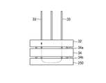
- the tester 300 includes a housing 31, a mother board 32 provided horizontally at the bottom of the housing 31, a plurality of test circuit boards 33 mounted in a standing state in slots of the mother board 32, a mother board 32, and a probe card. And a tester control unit 35.
- the mother board 32 is connected to the probe card 25 via the contact block 34.
- the contact block 34 performs connection with the mother board 32 and connection with the probe card 25 via a plurality of contact pins 34a and 34b, respectively.
- the contact pins 34a and 34b are pogo pins.
- the inspection circuit board 33 gives an electrical signal to the device on the wafer W according to various test items.
- the tester control unit 35 controls each component of the tester 300, a main control unit having a CPU, an input unit such as a keyboard, a mouse, and a remote controller, an output unit such as a printer, a display unit such as a display, and a control And a storage unit for storing necessary information.
- the main control unit sets a storage medium in which test items and the like are stored in the storage unit, thereby causing the tester 300 to execute a predetermined operation based on the test items called from the storage medium.
- the prober control unit 27 and the tester control unit 35 are each configured to record system operation history, operator operation history, diagnosis history, and other history information for the purpose of elucidating and coping with the cause of any failure.
- a history information acquisition unit (not shown) that acquires (log data) is included, and the history information acquired by the history information acquisition unit is stored in the history information storage / management unit 40.
- the failure analysis / prediction processing unit 400 has artificial intelligence (AI), and when a failure (FAIL) or a sign of failure occurs, the failure analysis / prediction processing unit 400 performs factor analysis on the information from the prober 200 or the tester 300, When the location is not known, the history information of the tester and prober related to the failure is obtained from the history information storage / management unit 40, and the location of the failure is determined based on the information and knowledge of an expert such as a service / developer. Know (identify or estimate) or predict.
- AI artificial intelligence
- the failure analysis / prediction processing unit 400 can acquire stage coordinate information, contact weight information, probe position / tilt information, and stage temperature as prober information from the history information storage / management unit 40.
- pin leak information, pin contact resistance, and pin power supply voltage / current information can be acquired as tester information.
- the host control unit 500 includes a main control unit having a CPU, an input unit such as a keyboard, a mouse, and a remote controller, an output unit such as a printer, a display unit such as a display, and a storage unit that stores information necessary for control. have.
- the host control unit 500 is a control unit that is higher than the prober control unit 27 and the tester control unit 35.
- the host control unit 500 transmits and receives information to the prober control unit 27 and the tester control unit 35, and converts the failure information into a failure analysis / prediction processing unit 400.
- To the failure analysis / prediction processing unit 400 receives information on the cause of the failure (or its sign), and displays the information on the display unit.
- the probe card 25 is mounted by the transfer unit 22 of the prober 200, and then the wafer W in the carrier is transferred onto the stage 26 by the transfer unit 22, and the wafer W is transferred onto the stage 26.
- the wafer W is subjected to an electrical inspection by the tester 300 while being vacuum-sucked.
- the probe card 25 is electrically connected to the mother board 32 via the contact block 34.
- the stage 26 is raised to bring the probe 25a of the probe card 25 into contact with each device (DUT) on the wafer W. Then, as shown in FIG. 3, the electrical signal from the inspection circuit board 33 reaches each device on the wafer W through the mother board 32, the contact block 34, and the probe card 25, and further from the device to the probe card 25, the contact block 34, Return to the inspection circuit board 33 through the mother board 32. Thereby, the electrical characteristics of each device are inspected.
- the voltage, current, logic waveform, etc. are output from the tester 300 to the device on the wafer, the voltage, current, and logic waveform from the device are measured, and the PASS and NG of the device are determined.
- test circuit board 33 to the wafer of the tester 300 are configured as shown in FIG. 3, the tester measurement accuracy, the position of the contact portion, the contact between the wafer W and the probe 25a, the position of the stage 26 (wafer chuck top), etc. Thus, the device on the wafer W is measured.
- failure analysis / prediction processing is performed.
- the program of the unit 400 is activated to deal with such a problem.
- the sign of the previous stage of failure refers to a case where the PASS level is divided into several stages, and even if it is PASS, it is determined that a failure will occur in the near future, which contributes to failure prediction. is there.
- ⁇ Failure analysis / prediction program> A flowchart of the failure analysis / prediction program at this time is shown in FIG. First, it is notified that a failure or a pre-failure sign has occurred (step 1).
- “failure” means that the measurement has become “FAIL”, and not only the original failure of the device component, but also that the device has not failed but has become “FAIL” due to dust or the like. Including.
- step 2 the information in the tester or the prober is acquired, and the factor analysis is performed with the information (step 2). It is determined whether or not the factor has been identified (step 3). If the factor has been identified, the process ends.
- the past history of the tester or prober in the history information storage / management unit 40 is searched (step 4).
- it is determined whether there is information on the failure (or indication) or information close to the failure (or indication) (step 5). If there is no close information, the other information (if the prober is the first analyzed is the information of the tester, the first analysis is the information of the prober if it is the information of the prober), in the past history Information on the failure (or indication) or information close to the failure (or indication) is analyzed (step 6).
- it is determined whether or not the failure (or indication) location and the analysis position are related (step 7). If so, the failure location is specified or estimated or the failure location is predicted (step 8) and registered as a history. (Step 9). And the result is displayed on a display part, for example. When a failure is predicted, it can be dealt with at a stage where no failure actually occurs.
- step 5 if there is information close in step 5, the failure location is specified or estimated or the failure location is predicted (step 8) and registered as a history (step 9). If the failure (or symptom) location and the analysis position are not related in step 7, another information is searched and the past history in step 6 is analyzed.
- the failure location can be grasped and predicted.
- the level in OK is set to 6 levels as shown in FIG.
- Level 0 in FIG. 7 is a level at which there is almost no possibility of failure, and approaches FAIL as the level increases from level 1 to level 5.
- the analysis / prediction processing unit 400 can predict a failure of a specific part (for example, a probe card or an inspection circuit board).
- ⁇ Analysis result display using wafer map> the method of dividing the PASS level into a plurality of stages can be used for the wafer map, and the analysis result can be confirmed by displaying the wafer map. Since failure analysis is basically performed on a device (DUT) basis, if a plurality of DUTs are PASS but the level is high and it is determined to be a pre-failure stage, the influence of this on multiple wafers on the wafer is determined. It can be confirmed on the wafer map displaying the DUT. For the display of the wafer map, it is possible to select display of only the latest result or display in which past results are superimposed.
- FIG. 8 to FIG. 10 show examples of failure analysis / prediction when a plurality of DUTs are FAIL or PASS using a wafer map capable of level display, but the level is high and it is determined to be a pre-failure stage. In these figures, the darker the color, the higher the level in FIG.
- FIG. 8 shows a case where a dark portion (high level) is generated in a linear shape on the wafer map.
- Each of the plurality of inspection circuit boards 33 corresponds to a different linear region among the plurality of DUTs on the wafer. Therefore, when the color is dark like this, one of the inspection circuit boards 33 is defective. It is thought that the cause is that it is in the previous stage of failure.
- FIG. 9 shows a case where a dark spot color (high level) occurs in a part of the wafer map. This is considered to be caused by a foreign object caught in the tip of the contact pin, and the contact of surrounding contact pins deteriorated due to the influence.
- FIG. 10 shows a case where an overall dark color (high level) portion is generated on the right side of the wafer map. This is considered to be because the contact of the wafer card or the probe is not uniform. For example, the state is as shown in FIG.
- the height of the stage is determined by displaying the variation with respect to the average height of the four points at the four points of the stage, for example, by 6 levels (levels 0 to 5) and FAIL in FIG. An example is shown in FIG. Also in FIG. 11, the darker the color, the higher the level of FIG. For example, the state is as shown in FIG. If there are variations in the height of the stage, it can be visually confirmed. In combination with the results shown in FIG. 10 above, it can be considered that there is an influence between the contact block and the tester due to the height variation of the stage 26.
- the cause of the abnormality is identified based on the history information of both the prober and the tester, so that the failure location can be identified or estimated quickly. it can.
- the failure location can be predicted before failure, so that the target part can be replaced or repaired in advance. For this reason, the operation rate of an inspection system can be improved.
- the present invention is not limited to the above-described embodiment, and various modifications can be made within the scope of the idea of the present invention.
- the flowchart of FIG. 4 is merely an example, and the present invention is not limited to this as long as failure analysis and failure prediction can be performed from both prober and tester information.
- the configuration of the inspection system is not limited to the above embodiment, and the inspection system may include a plurality of probers and a plurality of testers.
- substrate was shown, a board
Landscapes
- Engineering & Computer Science (AREA)
- Physics & Mathematics (AREA)
- General Physics & Mathematics (AREA)
- Computer Hardware Design (AREA)
- Microelectronics & Electronic Packaging (AREA)
- Manufacturing & Machinery (AREA)
- Power Engineering (AREA)
- General Engineering & Computer Science (AREA)
- Condensed Matter Physics & Semiconductors (AREA)
- Automation & Control Theory (AREA)
- Testing Or Measuring Of Semiconductors Or The Like (AREA)
- Tests Of Electronic Circuits (AREA)
- Testing Of Individual Semiconductor Devices (AREA)
- Health & Medical Sciences (AREA)
- Theoretical Computer Science (AREA)
- Environmental & Geological Engineering (AREA)
- Biophysics (AREA)
- Evolutionary Computation (AREA)
- General Health & Medical Sciences (AREA)
- Molecular Biology (AREA)
- Computing Systems (AREA)
- Mathematical Physics (AREA)
- Software Systems (AREA)
- Data Mining & Analysis (AREA)
- Computational Linguistics (AREA)
- Toxicology (AREA)
- Biomedical Technology (AREA)
- Artificial Intelligence (AREA)
- Life Sciences & Earth Sciences (AREA)
Abstract
An inspection device (100) having: a prober (200) that has a stage (26) holding a substrate (W) having a plurality of devices formed thereupon, a transport unit (22) that transports the substrate (W) to the stage (26), and a probe card (25) that causes a plurality of probes 25a to come in contact with electrodes in the plurality of devices upon the substrate (W); a tester (300) that applies an electric signal to the plurality of devices upon the substrate (W) via the probe card (25) and inspects the electrical characteristics of the devices; and a malfunction analysis/prediction unit (400) that, when a malfunction has occurred during inspection or a sign indicates a stage prior to a malfunction, analyzes history information for the prober (200) and tester (300) related to that malfunction and ascertains or predicts the location of the malfunction.
Description
本発明は、被検査体の検査を行う検査システム、および検査システムの故障解析・予知方法に関する。
The present invention relates to an inspection system for inspecting an object to be inspected, and a failure analysis / prediction method of the inspection system.
半導体デバイスの製造プロセスにおいては、半導体ウエハ(以下単にウエハと記す)における全てのプロセスが終了した段階で、ウエハに形成されている複数のデバイス(ICチップ)の電気的検査が行われる。このような電気的検査を行う検査システムは、一般的に、ウエハステージとウエハ搬送系を有するとともに、ウエハに形成されたデバイスに接触するプローブを有するプローブカードが装着されるプローバと、デバイスに電気的信号を与え、デバイスの種々の電気特性を検査するためのテスタとを有している。
In the manufacturing process of semiconductor devices, electrical inspection of a plurality of devices (IC chips) formed on a wafer is performed at the stage where all the processes on a semiconductor wafer (hereinafter simply referred to as a wafer) are completed. In general, an inspection system that performs such an electrical inspection includes a wafer stage and a wafer transfer system, a prober having a probe card having a probe that contacts a device formed on the wafer, and an electrical device connected to the device. And a tester for providing various signals and inspecting various electrical characteristics of the device.
このような検査システムにおいて、故障が発生したとき、その故障要因を迅速に特定して対処することが求められている。また、故障を事前に予知して故障を回避することも求められている。
In such an inspection system, when a failure occurs, it is required to quickly identify and deal with the cause of the failure. In addition, it is also required to predict a failure in advance and avoid the failure.
特許文献1には、プローバのコントローラに自己診断実行機能を持たせて、プローバにおける故障要因を特定する技術が記載されている。
Patent Document 1 describes a technique for specifying a failure factor in a prober by providing a prober controller with a self-diagnosis execution function.
ところで、テスタとプローバは、それぞれ別のメーカにより製造され、顧客納入後にこれらを一体化することが多く、診断機能を持たせる場合にも、テスタとプローバに別個に診断機能を設けることになる。
By the way, the tester and the prober are manufactured by different manufacturers, and are often integrated after delivery to the customer. Even when the diagnostic function is provided, the diagnostic function is provided separately for the tester and the prober.
しかし、テスタおよびプローバのそれぞれの診断機能を用いて故障解析を行う場合、テスタ起因でプローバの診断がFAIL(NG)の場合や、その逆の場合があり、そのような場合にはテスタおよびプローバが診断機能を有していても、故障箇所を把握することが困難である。また、故障予知を行おうとしても、同様に、テスタ起因でプローバの診断がFAIL(NG)の場合およびその逆の場合には十分な予知が行えない。
However, when failure analysis is performed using the diagnostic functions of the tester and prober, the prober's diagnosis may be FAIL (NG) due to the tester or vice versa. In such a case, the tester and prober Even if it has a diagnostic function, it is difficult to grasp the fault location. Similarly, even if failure prediction is performed, sufficient prediction cannot be performed when the prober diagnosis is FAIL (NG) and vice versa due to the tester.
したがって、本発明の目的は、テスタおよびプローバにまたがる要因の故障またはその前段階の兆候が生じた場合でもその箇所を迅速に把握することまたは予知することができる技術を提供することにある。
Therefore, an object of the present invention is to provide a technique capable of quickly grasping or predicting the location even when a failure of a factor straddling a tester and a prober or a sign of the previous stage occurs.
本発明の第1の観点によれば、複数のデバイスが形成された基板を保持するステージと、基板を前記ステージに搬送する搬送部と、複数のプローブを基板上の複数のデバイスの電極に接触させるプローブカードとを有するプローバと、前記プローブカードを介して前記基板上の複数のデバイスに電気的信号を与え、前記デバイスの電気特性を検査するテスタと、検査の際に故障が発生したとき、または前記故障の前段階の兆候が発生したときに、その故障に関連する前記プローバと前記テスタの履歴情報を解析して故障の箇所を特定もしくは推定、または予知する故障解析・予知処理部とを有することを特徴とする検査システムが提供される。
According to the first aspect of the present invention, a stage that holds a substrate on which a plurality of devices are formed, a transport unit that transports the substrate to the stage, and a plurality of probes that contact electrodes of the plurality of devices on the substrate. A prober having a probe card, a tester that provides an electrical signal to a plurality of devices on the substrate via the probe card, and inspects the electrical characteristics of the device, and when a failure occurs during the inspection, Or a failure analysis / prediction processing unit that identifies or estimates or predicts the location of a failure by analyzing the history information of the prober and the tester related to the failure when an indication of the previous stage of the failure occurs. There is provided an inspection system characterized by comprising:
本発明の第2の観点によれば、複数のデバイスが形成された基板を保持するステージと、基板を前記ステージに搬送する搬送部と、複数のプローブを基板上の複数のデバイスの電極に接触させるプローブカードとを有するプローバと、前記プローブカードを介して前記基板上の複数のデバイスに電気的信号を与え、前記デバイスの電気特性を検査するテスタとを有する検査システムにおいて、故障の箇所を特定もしくは推定または予知する故障解析・予知方法であって、検査の際に故障が発生したとき、または前記故障の前段階の兆候が発生したときに、その故障に関連する前記プローバと前記テスタの履歴情報を解析して故障の箇所を特定もしくは推定、または予知することを特徴とする検査システムの故障解析・予知方法が提供される。
According to the second aspect of the present invention, a stage that holds a substrate on which a plurality of devices are formed, a transport unit that transports the substrate to the stage, and a plurality of probes that contact electrodes of the plurality of devices on the substrate. In the inspection system, comprising a prober having a probe card to be operated and a tester for applying an electrical signal to the plurality of devices on the substrate via the probe card to inspect the electrical characteristics of the device Alternatively, a failure analysis / prediction method that estimates or predicts, when a failure occurs during inspection, or when a sign of the previous stage of the failure occurs, the history of the prober and the tester related to the failure A failure analysis / prediction method for an inspection system characterized by identifying, estimating, or predicting a failure location by analyzing information is provided.
上記第1の観点および第2の観点において、前記履歴情報と知見者の知見に基づいて故障の箇所を把握または予知することが好ましい。前記故障の要因が複数想定される場合、前記知見者の知見に基づいて、前記故障の要因を特定し、それにより故障の箇所を特定もしくは推定または予知することができる。
In the first and second aspects described above, it is preferable to grasp or predict the location of the failure based on the history information and the knowledge of the expert. When a plurality of causes of the failure are assumed, the cause of the failure can be specified based on the knowledge of the expert, and thereby the location of the failure can be specified, estimated, or predicted.
前記テスタは、マザーボードと、前記マザーボードに装着された複数の検査回路ボードとを有し、前記プローバに装着されたプローブカードと前記マザーボードとの間に、これらを接続するコンタクト部材が配置され、前記検査回路ボード、前記マザーボード、前記コンタクト部材、前記プローブカードのいずれかに生じた故障の箇所を特定もしくは推定または予知するようにすることができる。
The tester includes a motherboard and a plurality of inspection circuit boards mounted on the motherboard, and a contact member that connects them is disposed between the probe card mounted on the prober and the motherboard, It is possible to identify, estimate, or predict the location of a failure that has occurred in any of the inspection circuit board, the motherboard, the contact member, and the probe card.
基板に形成された複数のデバイスの検査において、接触不良または前記テスタから被検査体までの伝送経路の抵抗大となる故障が生じたとき、それに関するプローバ側の要因およびテスタ側の要因を含む複数の要因を把握し、それらの中で正常であることが分かっている要因、または所定の診断を行った結果正常な結果が得られたことにより正常であることがわかる要因を除外し、残った要因から故障箇所を特定もしくは推定または予知することができる。
In the inspection of a plurality of devices formed on a substrate, when a contact failure or a failure that causes a resistance increase in the transmission path from the tester to the object to be inspected, a plurality of factors including a prober side factor and a tester side factor related thereto The factors that are known to be normal, or the factors that are known to be normal by obtaining a normal result as a result of performing a predetermined diagnosis are excluded and remain The failure location can be identified, estimated or predicted from the factors.
検査の際にPASSになった検査項目について出力結果を複数段階にレベル分けし、複数の測定結果によるレベルの変化から故障の兆候を把握し、故障を予知することができる。この場合に、基板に形成された複数のデバイスを表示するマップにおいて、検査の際にPASSになった項目について出力結果を複数段階にレベル分けし、PASSと判断されたデバイスのレベルの分布図から故障箇所を予知することができる。また、前記マップの前記レベルの分布図と、前記プローバの被検査体のステージの高さの分布を関連付けることにより故障箇所を予知することができる。
The output results of inspection items that became PASS at the time of inspection can be divided into a plurality of levels, and a sign of failure can be grasped from a change in level based on a plurality of measurement results, so that the failure can be predicted. In this case, in the map that displays a plurality of devices formed on the substrate, the output result is divided into a plurality of levels for the items that became PASS at the time of inspection, and from the distribution chart of the level of the device determined to be PASS The failure location can be predicted. In addition, a failure location can be predicted by associating the distribution map of the level of the map with the distribution of the height of the stage of the inspection object of the prober.
本発明によれば、故障が発生した場合に、プローバおよびテスタの両方の履歴情報に基づいて異常の要因を特定するので、迅速に故障箇所の特定もしくは推定を行うことができる。また、故障の前段階の兆候が発生した場合に、故障する前に故障箇所を予知することができるので、事前に対象部品の交換や修理が可能となる。このため、検査システムの稼働率を向上させることができる。
According to the present invention, when a failure occurs, the cause of the abnormality is identified based on the history information of both the prober and the tester, so that the failure location can be identified or estimated quickly. In addition, when a sign of the previous stage of failure occurs, the failure location can be predicted before failure, so that the target part can be replaced or repaired in advance. For this reason, the operation rate of an inspection system can be improved.
以下、添付図面を参照して本発明の実施の形態について詳細に説明する。
<検査システム>
図1は、本発明の一実施形態に係る検査システムの概略構成を模式的に示す図である。検査システムは、ウエハにおける全てのプロセスが終了した段階で、ウエハに形成されている複数のデバイス(ICチップ;以下DUT(Device Under Test)ともいう)の電気的検査を行うものである。 Hereinafter, embodiments of the present invention will be described in detail with reference to the accompanying drawings.
<Inspection system>
FIG. 1 is a diagram schematically showing a schematic configuration of an inspection system according to an embodiment of the present invention. The inspection system performs an electrical inspection of a plurality of devices (IC chips; also referred to as DUT (Device Under Test) hereinafter) formed on the wafer at the stage where all processes on the wafer are completed.
図1に示すように、検査システム100は、ウエハ上のデバイスに対してプローブカードのプローブを接触させるプローバ200と、デバイスに電気信号を与えて電気的な検査を行うテスタ300と、故障解析・予知処理部400と、上位制御部500とを有している。
As shown in FIG. 1, an inspection system 100 includes a prober 200 that makes a probe of a probe card contact a device on a wafer, a tester 300 that performs an electrical inspection by giving an electrical signal to the device, a failure analysis / It has a prediction processing unit 400 and a host control unit 500.
プローバ200は、本体部21と、搬送部22と、プローバ制御部27とを有している。
The prober 200 includes a main body unit 21, a transport unit 22, and a prober control unit 27.
本体部21は、筐体23と、筐体23の天面を構成し、中央に円形の孔24aが形成されたヘッドプレート24と、ヘッドプレート24の孔24aに対応する位置に取り付けられ、複数のプローブ(接触子)25aを有するプローブカード25と、プローブカード25の下方位置でウエハWを載置し、吸着するステージ(ウエハチャックトップ)26とを有する。ステージ26は、X-Yテーブル機構、Z方向移動機構およびθ方向移動機構(いずれも図示せず)によりX、Y、Z、θ方向に移動可能となっており、ウエハWを所定の検査位置へ位置決めするようになっている。そして、ウエハWを上昇させることにより、プローブカード25のプローブ25aが複数のデバイスの電極に接触するようになっている。
The main body 21 is attached to a housing 23, a head plate 24 that forms the top surface of the housing 23, a circular hole 24a is formed in the center, and a position corresponding to the hole 24a of the head plate 24. A probe card 25 having a probe (contactor) 25a, and a stage (wafer chuck top) 26 on which the wafer W is placed and adsorbed at a position below the probe card 25. The stage 26 is movable in the X, Y, Z, and θ directions by an XY table mechanism, a Z direction moving mechanism, and a θ direction moving mechanism (all not shown), and the wafer W is moved to a predetermined inspection position. It is designed to be positioned. Then, by raising the wafer W, the probes 25a of the probe card 25 come into contact with the electrodes of a plurality of devices.
搬送部22は搬送装置(図示せず)を有するとともに、ウエハキャリアおよびプローブカードストッカ(いずれも図示せず)が装着されており、搬送装置により、ウエハキャリアからウエハWをステージ26上に搬送するとともに、プローブカードストッカからプローブカード25をヘッドプレート24の下方に搬送する。
The transfer unit 22 includes a transfer device (not shown), and a wafer carrier and a probe card stocker (both not shown) are mounted. The transfer device transfers the wafer W from the wafer carrier onto the stage 26. At the same time, the probe card 25 is conveyed below the head plate 24 from the probe card stocker.
プローバ制御部27は、プローバ200の各構成部を制御する、CPUを有する主制御部と、キーボードやマウス、リモコン等の入力部と、プリンター等の出力部と、ディスプレイ等の表示部と、制御に必要な情報を記憶する記憶部とを有している。主制御部は、検査に際して、記憶部に処理レシピが記憶された記憶媒体をセットすることにより、記憶媒体から呼び出された処理レシピに基づいてプローバ200に所定の処理動作を実行させる。
The prober control unit 27 controls each component of the prober 200, a main control unit having a CPU, an input unit such as a keyboard, a mouse, and a remote controller, an output unit such as a printer, a display unit such as a display, and a control And a storage unit for storing necessary information. At the time of inspection, the main control unit sets a storage medium in which the processing recipe is stored in the storage unit, thereby causing the prober 200 to execute a predetermined processing operation based on the processing recipe called from the storage medium.
テスタ300は、筐体31と、筐体31内の底部に水平に設けられたマザーボード32と、マザーボード32のスロットに立設状態で装着された複数の検査回路ボード33と、マザーボード32とプローブカード25とを接続するためのコンタクトブロック34と、テスタ制御部35とを有している。
The tester 300 includes a housing 31, a mother board 32 provided horizontally at the bottom of the housing 31, a plurality of test circuit boards 33 mounted in a standing state in slots of the mother board 32, a mother board 32, and a probe card. And a tester control unit 35.
マザーボード32は、コンタクトブロック34を介してプローブカード25に接続される。コンタクトブロック34は、マザーボード32との間の接続およびプローブカード25との間の接続を、それぞれ複数のコンタクトピン34aおよび34bを介して行う。コンタクトピン34aおよび34bはポゴピンで構成されている。検査回路ボード33は、種々のテスト項目に応じてウエハWのデバイスに電気的信号を与えるものである。
The mother board 32 is connected to the probe card 25 via the contact block 34. The contact block 34 performs connection with the mother board 32 and connection with the probe card 25 via a plurality of contact pins 34a and 34b, respectively. The contact pins 34a and 34b are pogo pins. The inspection circuit board 33 gives an electrical signal to the device on the wafer W according to various test items.
テスタ制御部35は、テスタ300の各構成部を制御する、CPUを有する主制御部と、キーボードやマウス、リモコン等の入力部と、プリンター等の出力部と、ディスプレイ等の表示部と、制御に必要な情報を記憶する記憶部とを有している。主制御部は、検査に際して、記憶部にテスト項目等が記憶された記憶媒体をセットすることにより、記憶媒体から呼び出されたテスト項目に基づいてテスタ300に所定の動作を実行させる。
The tester control unit 35 controls each component of the tester 300, a main control unit having a CPU, an input unit such as a keyboard, a mouse, and a remote controller, an output unit such as a printer, a display unit such as a display, and a control And a storage unit for storing necessary information. At the time of inspection, the main control unit sets a storage medium in which test items and the like are stored in the storage unit, thereby causing the tester 300 to execute a predetermined operation based on the test items called from the storage medium.
プローバ制御部27およびテスタ制御部35は、それぞれ、何等かの故障が発生した場合に、その原因の解明や対処を目的として、システムの動作履歴や操作者の操作履歴、診断履歴等の履歴情報(ログデータ)を取得する履歴情報取得部(図示せず)を有し、履歴情報取得部が取得した履歴情報は、履歴情報記憶・管理部40に記憶されるようになっている。
The prober control unit 27 and the tester control unit 35 are each configured to record system operation history, operator operation history, diagnosis history, and other history information for the purpose of elucidating and coping with the cause of any failure. A history information acquisition unit (not shown) that acquires (log data) is included, and the history information acquired by the history information acquisition unit is stored in the history information storage / management unit 40.
故障解析・予知処理部400は、人口知能(AI)を有しており、故障(FAIL)または故障の兆候が発生したときに、プローバ200またはテスタ300からの情報で要因解析を行い、それで故障箇所がわからない場合に、履歴情報記憶・管理部40から、その故障に関連するテスタおよびプローバの履歴情報を取得し、その情報とサービス・開発者等の知見者の知見に基づいて故障の箇所を把握(特定または推定)または予知する。
The failure analysis / prediction processing unit 400 has artificial intelligence (AI), and when a failure (FAIL) or a sign of failure occurs, the failure analysis / prediction processing unit 400 performs factor analysis on the information from the prober 200 or the tester 300, When the location is not known, the history information of the tester and prober related to the failure is obtained from the history information storage / management unit 40, and the location of the failure is determined based on the information and knowledge of an expert such as a service / developer. Know (identify or estimate) or predict.
図2に示すように、故障解析・予知処理部400は、履歴情報記憶・管理部40から、プローバ情報として、ステージ座標情報、コンタクト加重情報、プローブ位置・傾き情報、ステージ温度を取得することができ、テスタ情報として、ピンリーク情報、ピン接触抵抗、ピン電源電圧・電流情報を取得することができる。
As shown in FIG. 2, the failure analysis / prediction processing unit 400 can acquire stage coordinate information, contact weight information, probe position / tilt information, and stage temperature as prober information from the history information storage / management unit 40. In addition, pin leak information, pin contact resistance, and pin power supply voltage / current information can be acquired as tester information.
上位制御部500は、CPUを有する主制御部と、キーボードやマウス、リモコン等の入力部と、プリンター等の出力部と、ディスプレイ等の表示部と、制御に必要な情報を記憶する記憶部とを有している。上位制御部500は、プローバ制御部27およびテスタ制御部35の上位の制御部であり、プローバ制御部27およびテスタ制御部35に対する情報の授受を行うとともに、故障情報を故障解析・予知処理部400に送り、故障解析・予知処理部400から故障(またはその兆候)の要因に関する情報を受け取り、その情報を表示部に表示する。
The host control unit 500 includes a main control unit having a CPU, an input unit such as a keyboard, a mouse, and a remote controller, an output unit such as a printer, a display unit such as a display, and a storage unit that stores information necessary for control. have. The host control unit 500 is a control unit that is higher than the prober control unit 27 and the tester control unit 35. The host control unit 500 transmits and receives information to the prober control unit 27 and the tester control unit 35, and converts the failure information into a failure analysis / prediction processing unit 400. To the failure analysis / prediction processing unit 400, receives information on the cause of the failure (or its sign), and displays the information on the display unit.
<検査方法>
このように構成された検査システム100においては、プローバ200の搬送部22によりプローブカード25を装着し、次いで搬送部22によりキャリア内のウエハWをステージ26上に搬送し、ウエハWをステージ26上に真空吸着した状態で、ウエハWに対してテスタ300により、電気的検査を行う。このとき、プローブカード25はコンタクトブロック34を介してマザーボード32に電気的に接続されている。 <Inspection method>
In theinspection system 100 configured as described above, the probe card 25 is mounted by the transfer unit 22 of the prober 200, and then the wafer W in the carrier is transferred onto the stage 26 by the transfer unit 22, and the wafer W is transferred onto the stage 26. The wafer W is subjected to an electrical inspection by the tester 300 while being vacuum-sucked. At this time, the probe card 25 is electrically connected to the mother board 32 via the contact block 34.
このように構成された検査システム100においては、プローバ200の搬送部22によりプローブカード25を装着し、次いで搬送部22によりキャリア内のウエハWをステージ26上に搬送し、ウエハWをステージ26上に真空吸着した状態で、ウエハWに対してテスタ300により、電気的検査を行う。このとき、プローブカード25はコンタクトブロック34を介してマザーボード32に電気的に接続されている。 <Inspection method>
In the
検査に際しては、ステージ26を上昇させてプローブカード25のプローブ25aをウエハWの各デバイス(DUT)に接触させる。そして、図3に示すように、検査回路ボード33からの電気信号が、マザーボード32、コンタクトブロック34、プローブカード25を経てウエハWの各デバイスに至り、さらにデバイスからプローブカード25、コンタクトブロック34、マザーボード32を経て検査回路ボード33に戻る。これにより各デバイスの電気的特性が検査される。
In the inspection, the stage 26 is raised to bring the probe 25a of the probe card 25 into contact with each device (DUT) on the wafer W. Then, as shown in FIG. 3, the electrical signal from the inspection circuit board 33 reaches each device on the wafer W through the mother board 32, the contact block 34, and the probe card 25, and further from the device to the probe card 25, the contact block 34, Return to the inspection circuit board 33 through the mother board 32. Thereby, the electrical characteristics of each device are inspected.
具体的には、テスタ300からウエハ上のデバイスに対して、電圧、電流、ロジック波形等を出力し、デバイスからの電圧、電流、ロジック波形を測定し、デバイスのPASSおよびNGを判断する。
Specifically, the voltage, current, logic waveform, etc. are output from the tester 300 to the device on the wafer, the voltage, current, and logic waveform from the device are measured, and the PASS and NG of the device are determined.
テスタ300の検査回路ボード33からウエハまでは図3のような構成となっているため、テスタ測定精度、コンタクト部の位置、ウエハWとプローブ25aの接触、ステージ26(ウエハチャックトップ)の位置等の複数の要因が含まれてウエハW上のデバイスの測定に至っている。
Since the test circuit board 33 to the wafer of the tester 300 are configured as shown in FIG. 3, the tester measurement accuracy, the position of the contact portion, the contact between the wafer W and the probe 25a, the position of the stage 26 (wafer chuck top), etc. Thus, the device on the wafer W is measured.
そのため、上記の構成上のどこかに不具合があった場合、ウエハの測定不良(故障)が発生するが、従来は、その要因がどこにあるのかが容易に特定できないことがあった。その理由の一つとして、従来、テスタの情報とプローバの情報を別個に管理していたため、テスタおよびプローバの一方が他方の要因で不良(故障)を起こした場合は、その要因を特定できないことが挙げられる。また、故障を予知して事前に対応することが求められるが、このようにテスタの情報とプローバの情報を別個に管理する場合は、故障の予知も困難である。
Therefore, if there is a problem somewhere on the above configuration, a measurement failure (failure) of the wafer occurs. However, conventionally, there is a case where the cause is not easily identified. One of the reasons is that the tester information and the prober information have been managed separately in the past, so if one of the tester and the prober fails (failure) due to the other factor, the cause cannot be specified. Is mentioned. In addition, it is required to predict a failure and deal with it in advance, but when the tester information and the prober information are separately managed in this way, it is difficult to predict the failure.
そこで、本実施形態では、検査のときに不良(FAIL)となった際、すなわち何らかの故障が生じた場合に、またはFAILではないが故障の前段階の兆候が生じた場合、故障解析・予知処理部400のプログラムが起動されるようにし、このような問題に対処する。なお、故障の前段階の兆候とは、後述するように、PASSのレベルを何段階かに分け、PASSであっても近い将来に故障となると判断される場合をいい、故障予知に資するものである。
Therefore, in the present embodiment, when a failure (FAIL) occurs at the time of inspection, that is, when some failure occurs, or when a symptom before failure occurs that is not FAIL, failure analysis / prediction processing is performed. The program of the unit 400 is activated to deal with such a problem. In addition, as described later, the sign of the previous stage of failure refers to a case where the PASS level is divided into several stages, and even if it is PASS, it is determined that a failure will occur in the near future, which contributes to failure prediction. is there.
<故障解析・予知プログラム>
このときの故障解析・予知プログラムのフローチャートを図4に示す。
まず、故障または故障の前段階の兆候が発生したことが通知される(ステップ1)。なお、ここで「故障」とは、測定が「FAIL」になったことをいい、装置構成部の本来の故障のみならず、装置は故障していないがゴミ等により「FAIL」になったことも含む。 <Failure analysis / prediction program>
A flowchart of the failure analysis / prediction program at this time is shown in FIG.
First, it is notified that a failure or a pre-failure sign has occurred (step 1). Here, “failure” means that the measurement has become “FAIL”, and not only the original failure of the device component, but also that the device has not failed but has become “FAIL” due to dust or the like. Including.
次に、テスタ内またはプローバ内の情報を取得しその情報で要因解析を行う(ステップ2)。要因の特定ができたか否かを判断し(ステップ3)、要因が特定できた場合は終了する。
Next, the information in the tester or the prober is acquired, and the factor analysis is performed with the information (step 2). It is determined whether or not the factor has been identified (step 3). If the factor has been identified, the process ends.
要因の特定ができない場合は、履歴情報記憶・管理部40のテスタまたはプローバの過去の履歴を検索する(ステップ4)。次に、その故障(もしくは兆候)の情報またはその故障(もしくは兆候)に近い情報があるか否かを判断する(ステップ5)。近い情報がない場合、他方の情報(最初に解析したのがプローバの場合はテスタの情報であり、最初に解析したのがテスタの情報の場合はプローバの情報)で、過去の履歴の中でその故障(もしくは兆候)の情報または故障(もしくは兆候)に近い情報を解析する(ステップ6)。次に、故障(もしくは兆候)箇所と解析位置とが関連するかを判断し(ステップ7)、関連する場合は、故障箇所を特定もしくは推定または故障箇所を予知し(ステップ8)、履歴として登録する(ステップ9)。そして、その結果は、例えば表示部に表示される。故障を予知した場合には、実際に故障は生じていない段階で対処することができる。
If the cause cannot be specified, the past history of the tester or prober in the history information storage / management unit 40 is searched (step 4). Next, it is determined whether there is information on the failure (or indication) or information close to the failure (or indication) (step 5). If there is no close information, the other information (if the prober is the first analyzed is the information of the tester, the first analysis is the information of the prober if it is the information of the prober), in the past history Information on the failure (or indication) or information close to the failure (or indication) is analyzed (step 6). Next, it is determined whether or not the failure (or indication) location and the analysis position are related (step 7). If so, the failure location is specified or estimated or the failure location is predicted (step 8) and registered as a history. (Step 9). And the result is displayed on a display part, for example. When a failure is predicted, it can be dealt with at a stage where no failure actually occurs.
一方、上記ステップ5で近い情報がある場合、故障箇所を特定もしくは推定または故障箇所を予知し(ステップ8)、履歴として登録する(ステップ9)。また、ステップ7で、故障(もしくは兆候)箇所と解析位置とが関連しない場合は、別の情報を検索して、ステップ6の過去の履歴の解析を行う。
On the other hand, if there is information close in step 5, the failure location is specified or estimated or the failure location is predicted (step 8) and registered as a history (step 9). If the failure (or symptom) location and the analysis position are not related in step 7, another information is searched and the past history in step 6 is analyzed.
<故障解析・予知の実例>
次に、故障解析・予知の実例について説明する。
例えば、図5に示すように、プローブカード25の設置が正常でない場合、ウエハ検査において、接触不良(オープン)、または、テスタからウエハまでの伝送経路の抵抗大により、検査結果不良が発生する。 <Examples of failure analysis and prediction>
Next, an example of failure analysis / prediction will be described.
For example, as shown in FIG. 5, when theprobe card 25 is not properly installed, an inspection result failure occurs due to a contact failure (open) or a large resistance of the transmission path from the tester to the wafer in the wafer inspection.
次に、故障解析・予知の実例について説明する。
例えば、図5に示すように、プローブカード25の設置が正常でない場合、ウエハ検査において、接触不良(オープン)、または、テスタからウエハまでの伝送経路の抵抗大により、検査結果不良が発生する。 <Examples of failure analysis and prediction>
Next, an example of failure analysis / prediction will be described.
For example, as shown in FIG. 5, when the
接触不良または伝送経路の抵抗大のときの発生要因としては、以下の(1)~(5)の複数の要因が考えられる。
(1)コンタクトブロック34のテスタ側のコンタクト
(2)コンタクトブロック34のプローブカード側のコンタクト
(3)プローブ25aとウエハWのコンタクト
(4)ステージ26(チャックトップ)の水平不良→ステージの高さ情報から判断
(5)テスタ出力および測定不良等→テスタ診断結果から判断 The following factors (1) to (5) are conceivable as the generation factors when the contact failure or the resistance of the transmission path is large.
(1) Contact on the tester side of the contact block 34 (2) Contact on the probe card side of the contact block 34 (3) Contact between theprobe 25a and the wafer W (4) Horizontal failure of the stage 26 (chuck top) → Stage height Judgment from information (5) Tester output and measurement failure → Judgment from tester diagnosis result
(1)コンタクトブロック34のテスタ側のコンタクト
(2)コンタクトブロック34のプローブカード側のコンタクト
(3)プローブ25aとウエハWのコンタクト
(4)ステージ26(チャックトップ)の水平不良→ステージの高さ情報から判断
(5)テスタ出力および測定不良等→テスタ診断結果から判断 The following factors (1) to (5) are conceivable as the generation factors when the contact failure or the resistance of the transmission path is large.
(1) Contact on the tester side of the contact block 34 (2) Contact on the probe card side of the contact block 34 (3) Contact between the
既にこの時点で、テスタ診断結果およびステージ26の高さの情報で、これらが正常であることがわかっていれば、コンタクトブロック34およびプローブカード周辺での不良(故障)が推測される。
At this point in time, if it is known from the tester diagnosis result and the height information of the stage 26 that these are normal, a defect (failure) around the contact block 34 and the probe card is estimated.
さらに、図6に示すように、診断用プローブカード250で診断を行った結果、正常な結果が得られていれば、上記(1)および(2)が正常であることがわかり、要因は(3)のプローブカードによる接触不良と推測(特定)することができ、故障箇所を把握することができる。また、後述するようにPASSのレベルを複数レベルに設定しておけば、これらにより故障箇所の予知を行うことができる。
Furthermore, as shown in FIG. 6, if a normal result is obtained as a result of diagnosis with the diagnostic probe card 250, it can be seen that the above (1) and (2) are normal, and the cause is ( It is possible to infer (specify) contact failure due to the probe card of 3), and to grasp the failure location. Further, if the PASS level is set to a plurality of levels as will be described later, the failure location can be predicted by these.
このように、テスタ300およびプローバ200からの情報と、サービス・開発者等の装置知見者による要因解析プロセスに関する知見に基づいて、故障箇所の把握・予知が可能となる。
Thus, based on the information from the tester 300 and the prober 200 and the knowledge about the factor analysis process by the device experts such as the service / developer, the failure location can be grasped and predicted.
<故障予知>
次に、故障予知について詳細に説明する。
テスタ300によるウエハW上のデバイス(DUT)の検査においては、デバイスごとに検査結果が得られ、OK(PASS)であっても、全く問題のないレベルからFAILに近いレベルまで存在する。 <Failure prediction>
Next, failure prediction will be described in detail.
In the inspection of the device (DUT) on the wafer W by thetester 300, an inspection result is obtained for each device, and even if OK (PASS), it exists from a level at which there is no problem to a level close to FAIL.
次に、故障予知について詳細に説明する。
テスタ300によるウエハW上のデバイス(DUT)の検査においては、デバイスごとに検査結果が得られ、OK(PASS)であっても、全く問題のないレベルからFAILに近いレベルまで存在する。 <Failure prediction>
Next, failure prediction will be described in detail.
In the inspection of the device (DUT) on the wafer W by the
複数の検査項目に対して、OK(PASS)内のレベルを例えば図7に示すように、6段階に設定する。図7のレベル0は、故障の可能性がほとんどないレベルであり、レベル1~5とレベルが高くなるに従ってFAILに近づいて行く。
For the plurality of inspection items, the level in OK (PASS) is set to 6 levels as shown in FIG. Level 0 in FIG. 7 is a level at which there is almost no possibility of failure, and approaches FAIL as the level increases from level 1 to level 5.
例えばある検査項目(機能)について、複数日または複数回の測定結果を使用する。複数の測定結果が全てレベル0であれば、この検査項目(機能)は高い水準で正常であり、現時点では故障の可能性は低いと判断できる。しかし、時間経過に従って、測定結果がレベル1、2、3と上昇していけば、将来的に故障(FAIL)に至る可能性が高く、上昇の時間間隔が所定の値になったときに、故障の前段階の兆候ありとする。これにより、故障時期を予測することができる。その結果、事前に当該部品の交換、修理が可能となる。また、同じように、別項目もレベル分けを行い、上述のように比較、参照することで、故障の要因箇所の特定も可能となる。
For example, use measurement results for multiple days or multiple times for a certain inspection item (function). If all of the plurality of measurement results are level 0, it can be determined that this inspection item (function) is normal at a high level and the possibility of failure is low at the present time. However, if the measurement results rise to levels 1, 2, and 3 over time, there is a high possibility that a failure (FAIL) will occur in the future, and when the rise time interval reaches a predetermined value, Suppose there is a sign of the previous stage of failure. Thereby, the failure time can be predicted. As a result, the parts can be replaced and repaired in advance. Similarly, another item is classified into levels, and comparison and reference are made as described above, so that the cause of the failure can be specified.
例えば、ユーザーが検査システムを用いてウエハの検査を行った際、歩留まりが以前と比較して悪くなったとする。例えば最終的に図3の構造において接触抵抗が大の箇所があるとされる場合、従来はその箇所の特定が困難であり、故障予知ができなかった。その理由は、従来、各診断項目についてウエハの全てのデバイスの検査を行っているものの、その結果はPASSとFAILでしかなく、段階的な評価ができなかったからである。
Suppose, for example, that when a user inspects a wafer using an inspection system, the yield is worse than before. For example, when it is finally assumed that there is a portion having a large contact resistance in the structure of FIG. 3, it is conventionally difficult to specify the portion, and failure prediction cannot be performed. The reason is that all the devices on the wafer have been inspected for each diagnosis item, but the results are only PASS and FAIL, and stepwise evaluation has not been possible.
これに対し、上述のようにPASSのレベルを複数段階に分けることにより、故障の前段階の兆候を把握することができ、かつ複数項目を合わせてその箇所も特定できるので、それに基づいて、故障解析・予知処理部400により、特定部分(例えば、プローブカード、検査回路ボード)の故障の予知を行うことができる。
On the other hand, by dividing the PASS level into a plurality of stages as described above, the signs of the previous stage of the failure can be grasped, and the location can be specified by combining a plurality of items. The analysis / prediction processing unit 400 can predict a failure of a specific part (for example, a probe card or an inspection circuit board).
<ウエハマップを用いた解析結果表示>
このようにPASSのレベルを複数段階に分ける手法をウエハマップに用い、ウエハマップを表示して解析結果を確認することができる。故障解析は基本的にデバイス(DUT)単位で行うため、複数のDUTがPASSではあるがレベルが高く故障の前段階と判断された場合、これがどの影響で発生しているかをウエハ上の複数のDUTを表示したウエハマップで確認することができる。ウエハマップの表示は、直近の結果のみの表示と、過去の結果を重ね合せた表示の選択が可能である。 <Analysis result display using wafer map>
In this way, the method of dividing the PASS level into a plurality of stages can be used for the wafer map, and the analysis result can be confirmed by displaying the wafer map. Since failure analysis is basically performed on a device (DUT) basis, if a plurality of DUTs are PASS but the level is high and it is determined to be a pre-failure stage, the influence of this on multiple wafers on the wafer is determined. It can be confirmed on the wafer map displaying the DUT. For the display of the wafer map, it is possible to select display of only the latest result or display in which past results are superimposed.
レベル表示可能なウエハマップを用いて複数のDUTがFAIL、またはPASSではあるがレベルが高く故障の前段階と判断された場合の故障解析・予知の例を図8~図10に示す。これらの図において、色が濃いほど図7のレベルが高いことを示す。
FIG. 8 to FIG. 10 show examples of failure analysis / prediction when a plurality of DUTs are FAIL or PASS using a wafer map capable of level display, but the level is high and it is determined to be a pre-failure stage. In these figures, the darker the color, the higher the level in FIG.
図8は、ウエハマップに線状に色が濃い(レベルが高い)部分が生じる場合である。複数の検査回路ボード33は、それぞれ、ウエハ上の複数のDUTのうち異なる線状領域に対応しているため、このように線状に色が濃い場合は、検査回路ボード33の一枚が故障しているか、故障の前段階であることが要因であると考えられる。
FIG. 8 shows a case where a dark portion (high level) is generated in a linear shape on the wafer map. Each of the plurality of inspection circuit boards 33 corresponds to a different linear region among the plurality of DUTs on the wafer. Therefore, when the color is dark like this, one of the inspection circuit boards 33 is defective. It is thought that the cause is that it is in the previous stage of failure.
図9は、ウエハマップの一部にスポット的に色が濃い(レベルが高い)部分が生じる場合である。これは、コンタクトピンの先端に異物が挟まり、その影響で周りのコンタクトピンの接触が悪くなったことが要因と考えられる。
FIG. 9 shows a case where a dark spot color (high level) occurs in a part of the wafer map. This is considered to be caused by a foreign object caught in the tip of the contact pin, and the contact of surrounding contact pins deteriorated due to the influence.
図10は、ウエハマップの右側に全体的に色が濃い(レベルが高い)部分が生じる場合である。これは、ウエハカードまたはプローブの接触が均一になっていないことが要因と考えられる。例えば、図5のような状態である。
FIG. 10 shows a case where an overall dark color (high level) portion is generated on the right side of the wafer map. This is considered to be because the contact of the wafer card or the probe is not uniform. For example, the state is as shown in FIG.
<ステージ(ウエハチャックトップ)の高さ>
ステージの高さは、ステージの4点において、4点の高さ平均に対するバラツキを例えば図7の6段階(レベル0~5)およびFAILで判定し表示する。その例を図11に示す。図11においても、色が濃いほど図7のレベルが高いことを示す。例えば、図12のような状態である。ステージの高さにバラツキがあった場合、視覚的に確認することができる。上記図10の結果も合わせれば、ステージ26の高さバラツキに起因して、コンタクトブロックからテスタまでの間に影響を与えることも考えられる。 <Stage (wafer chuck top) height>
The height of the stage is determined by displaying the variation with respect to the average height of the four points at the four points of the stage, for example, by 6 levels (levels 0 to 5) and FAIL in FIG. An example is shown in FIG. Also in FIG. 11, the darker the color, the higher the level of FIG. For example, the state is as shown in FIG. If there are variations in the height of the stage, it can be visually confirmed. In combination with the results shown in FIG. 10 above, it can be considered that there is an influence between the contact block and the tester due to the height variation of the stage 26.
ステージの高さは、ステージの4点において、4点の高さ平均に対するバラツキを例えば図7の6段階(レベル0~5)およびFAILで判定し表示する。その例を図11に示す。図11においても、色が濃いほど図7のレベルが高いことを示す。例えば、図12のような状態である。ステージの高さにバラツキがあった場合、視覚的に確認することができる。上記図10の結果も合わせれば、ステージ26の高さバラツキに起因して、コンタクトブロックからテスタまでの間に影響を与えることも考えられる。 <Stage (wafer chuck top) height>
The height of the stage is determined by displaying the variation with respect to the average height of the four points at the four points of the stage, for example, by 6 levels (
以上のように、本実施形態によれば、故障が発生した場合に、プローバおよびテスタの両方の履歴情報に基づいて異常の要因を特定するので、迅速に故障箇所の特定もしくは推定を行うことができる。また、故障の前段階の兆候が発生した場合に、故障する前に故障箇所を予知することができるので、事前に対象部品の交換や修理が可能となる。このため、検査システムの稼働率を向上させることができる。
As described above, according to the present embodiment, when a failure occurs, the cause of the abnormality is identified based on the history information of both the prober and the tester, so that the failure location can be identified or estimated quickly. it can. In addition, when a sign of the previous stage of failure occurs, the failure location can be predicted before failure, so that the target part can be replaced or repaired in advance. For this reason, the operation rate of an inspection system can be improved.
<他の適用>
なお、本発明は上記実施形態に限定されることなく、本発明の思想の範囲内において種々変形可能である。例えば、上記実施形態において、図4のフローチャートは例示に過ぎず、プローバおよびテスタの両方の情報から故障解析および故障予知ができればこれに限定されない。また、検査システムの構成も上記実施形態に限定されず、また、検査システムが複数のプローバおよび複数のテスタを含んでいてもよい。さらに、基板として半導体ウエハを用いた例を示したが、基板は半導体ウエハに限るものではない。 <Other applications>
The present invention is not limited to the above-described embodiment, and various modifications can be made within the scope of the idea of the present invention. For example, in the above embodiment, the flowchart of FIG. 4 is merely an example, and the present invention is not limited to this as long as failure analysis and failure prediction can be performed from both prober and tester information. The configuration of the inspection system is not limited to the above embodiment, and the inspection system may include a plurality of probers and a plurality of testers. Furthermore, although the example which used the semiconductor wafer as a board | substrate was shown, a board | substrate is not restricted to a semiconductor wafer.
21;本体部、22;搬送部、23;筐体、24;ヘッドプレート、25;プローブカード、25a;プローブ、26;ステージ(ウエハチャックトップ)、27;プローバ制御部、31;筐体、32;マザーボード、33;検査回路ボード、34;コンタクトブロック、35;テスタ制御部、40;履歴情報記憶・管理部、100;検査システム、200;プローバ、300;テスタ、400;故障解析・予知処理部、500;上位制御部
21; body part, 22; transfer part, 23; housing, 24; head plate, 25; probe card, 25a; probe, 26; stage (wafer chuck top), 27; prober control part, 31; ; Motherboard, 33; Inspection circuit board, 34; Contact block, 35; Tester control unit, 40; History information storage / management unit, 100; Inspection system, 200; Prober, 300; Tester, 400; Failure analysis / prediction processing unit , 500; host control unit
Claims (16)
- 複数のデバイスが形成された基板を保持するステージと、基板を前記ステージに搬送する搬送部と、複数のプローブを基板上の複数のデバイスの電極に接触させるプローブカードとを有するプローバと、
前記プローブカードを介して前記基板上の複数のデバイスに電気的信号を与え、前記デバイスの電気特性を検査するテスタと、
検査の際に故障が発生したとき、または前記故障の前段階の兆候が発生したときに、その故障に関連する前記プローバと前記テスタの履歴情報を解析して故障の箇所を特定もしくは推定、または予知する故障解析・予知処理部と、
を有することを特徴とする検査システム。 A prober having a stage for holding a substrate on which a plurality of devices are formed, a transport unit for transporting the substrate to the stage, and a probe card for bringing the plurality of probes into contact with electrodes of the plurality of devices on the substrate;
A tester for applying an electrical signal to a plurality of devices on the substrate via the probe card and inspecting electrical characteristics of the devices;
When a failure occurs during inspection, or when an indication of the previous stage of the failure occurs, the history information of the prober and the tester related to the failure is analyzed to identify or estimate the location of the failure, or The failure analysis / prediction processing unit to predict,
An inspection system comprising: - 前記故障解析・予知処理部は、前記履歴情報と知見者の知見に基づいて故障の箇所を特定もしくは推定、または予知することを特徴とする請求項1に記載の検査システム。 The inspection system according to claim 1, wherein the failure analysis / prediction processing unit specifies, estimates, or predicts a failure location based on the history information and knowledge of an expert.
- 前記故障の要因が複数想定される場合、前記知見者の知見に基づいて、前記故障の要因を特定し、それにより故障の箇所を特定もしくは推定、または予知することを特徴とする請求項2に記載の検査システム。 3. The method according to claim 2, wherein when a plurality of factors of the failure are assumed, the factor of the failure is identified based on the knowledge of the expert, thereby identifying or estimating or predicting the location of the failure. The inspection system described.
- 前記テスタは、マザーボードと、前記マザーボードに装着された複数の検査回路ボードとを有し、前記プローバに装着されたプローブカードと前記マザーボードとの間に、これらを接続するコンタクト部材が配置され、前記検査回路ボード、前記マザーボード、前記コンタクト部材、前記プローブカードのいずれかに生じた故障の箇所を特定または推定または予知することを特徴とする請求項1から請求項3のいずれか1項に記載の検査システム。 The tester includes a motherboard and a plurality of inspection circuit boards mounted on the motherboard, and a contact member that connects them is disposed between the probe card mounted on the prober and the motherboard, 4. The method according to claim 1, wherein a fault location occurring in any of the inspection circuit board, the motherboard, the contact member, and the probe card is specified, estimated, or predicted. 5. Inspection system.
- 基板に形成された複数のデバイスの検査において、接触不良または前記テスタから被検査体までの伝送経路の抵抗が大となる故障が生じたとき、
それに関するプローバ側の要因およびテスタ側の要因を含む複数の要因を把握し、それらの中で正常であることが分かっている要因、または所定の診断を行った結果正常な結果が得られたことにより正常であることがわかる要因を除外し、残った要因から故障箇所を特定もしくは推定または予知することを特徴とする請求項4に記載の検査システム。 In the inspection of a plurality of devices formed on the substrate, when a contact failure or a failure that increases the resistance of the transmission path from the tester to the object to be inspected occurs,
Understanding the factors on the prober side and the factors on the tester side in relation to them, factors that are known to be normal among them, or normal results obtained as a result of performing a predetermined diagnosis 5. The inspection system according to claim 4, wherein a factor that is known to be normal is excluded, and a fault location is identified, estimated, or predicted from the remaining factor. - 検査の際にPASSになった検査項目について出力結果を複数段階にレベル分けし、複数の測定結果によるレベルの変化から故障の兆候を把握し、故障を予知することを特徴とする請求項1から請求項5のいずれか1項に記載の検査システム。 The output result is divided into a plurality of levels for the inspection item that becomes PASS at the time of the inspection, the sign of failure is grasped from the change in level based on the plurality of measurement results, and the failure is predicted. The inspection system according to claim 5.
- 基板に形成された複数のデバイスを表示するマップにおいて、検査の際にPASSになった項目について出力結果を複数段階にレベル分けし、PASSと判断されたデバイスのレベルの分布図から故障箇所を予知することを特徴とする請求項6に記載の検査システム。 In the map that displays multiple devices formed on the substrate, the output results for the items that became PASS at the time of inspection are divided into multiple stages, and the failure location is predicted from the distribution map of the device level determined to be PASS The inspection system according to claim 6.
- 前記マップの前記レベルの分布図と、前記プローバの被検査体のステージの高さの分布を関連付けることにより故障箇所を予知することを特徴とする請求項7に記載の検査システム。 The inspection system according to claim 7, wherein a failure location is predicted by associating the distribution map of the level of the map with the distribution of the height of the stage of the probe to be inspected.
- 複数のデバイスが形成された基板を保持するステージと、基板を前記ステージに搬送する搬送部と、複数のプローブを基板上の複数のデバイスの電極に接触させるプローブカードとを有するプローバと、前記プローブカードを介して前記基板上の複数のデバイスに電気的信号を与え、前記デバイスの電気特性を検査するテスタとを有する検査システムにおいて、故障の箇所を把握または予知する故障解析・予知方法であって、
検査の際に故障が発生したとき、または前記故障の前段階の兆候が発生したときに、その故障に関連する前記プローバと前記テスタの履歴情報を解析して故障の箇所を特定もしくは推定、または予知することを特徴とする検査システムの故障解析・予知方法。 A prober having a stage for holding a substrate on which a plurality of devices are formed, a transport unit for transporting the substrate to the stage, and a probe card for bringing a plurality of probes into contact with electrodes of a plurality of devices on the substrate, and the probe A failure analysis / prediction method for grasping or predicting a location of a failure in an inspection system having a tester for applying electrical signals to a plurality of devices on the substrate via a card and inspecting electrical characteristics of the devices. ,
When a failure occurs during inspection, or when an indication of the previous stage of the failure occurs, the history information of the prober and the tester related to the failure is analyzed to identify or estimate the location of the failure, or A failure analysis / prediction method for an inspection system characterized by prediction. - 前記履歴情報と知見者の知見に基づいて故障の箇所を特定もしくは推定または予知することを特徴とする請求項9に記載の検査システムの故障解析・予知方法。 10. The failure analysis / prediction method for an inspection system according to claim 9, wherein a failure location is specified, estimated, or predicted based on the history information and the knowledge of an expert.
- 前記故障の要因が複数想定される場合、前記知見者の知見に基づいて、前記故障の要因を特定し、それにより故障の箇所を特定もしくは推定または予知することを特徴とする請求項10に記載の検査システムの故障解析・予知方法。 11. The method according to claim 10, wherein when a plurality of causes of the failure are assumed, the cause of the failure is specified based on the knowledge of the inspector, thereby identifying or estimating or predicting the location of the failure. Analysis and prediction method for inspection system
- 前記テスタは、マザーボードと、前記マザーボードに装着された複数の検査回路ボードとを有し、前記プローバに装着されたプローブカードと前記マザーボードとの間に、これらを接続するコンタクト部材が配置され、前記検査回路ボード、前記マザーボード、前記コンタクト部材、前記プローブカードのいずれかに生じた故障の箇所を特定もしくは推定、または予知することを特徴とする請求項9から請求項11のいずれか1項に記載の検査システムの故障解析・予知方法。 The tester includes a motherboard and a plurality of inspection circuit boards mounted on the motherboard, and a contact member that connects them is disposed between the probe card mounted on the prober and the motherboard, 12. The device according to claim 9, wherein a fault location occurring in any of the inspection circuit board, the motherboard, the contact member, and the probe card is specified, estimated, or predicted. Analysis and prediction method for inspection system
- 基板に形成された複数のデバイスの検査において、接触不良または前記テスタから被検査体までの伝送経路の抵抗が大となる故障が生じたとき、
それに関するプローバ側の要因およびテスタ側の要因を含む複数の要因を把握し、それらの中で正常であることが分かっている要因、または所定の診断を行った結果正常な結果が得られたことにより正常であることがわかる要因を除外し、残った要因から故障箇所を特定もしくは推定または予知することを特徴とする請求項12に記載の検査システムの故障解析・予知方法。 In the inspection of a plurality of devices formed on the substrate, when a contact failure or a failure that increases the resistance of the transmission path from the tester to the object to be inspected occurs,
Understanding the factors on the prober side and the factors on the tester side in relation to them, factors that are known to be normal among them, or normal results obtained as a result of performing a predetermined diagnosis 13. The inspection system failure analysis / prediction method according to claim 12, wherein a factor that is found to be normal is excluded, and a failure location is identified, estimated, or predicted from the remaining factor. - 検査の際にPASSになった検査項目について出力結果を複数段階にレベル分けし、複数の測定結果によるレベルの変化から故障の兆候を把握し、故障を予知することを特徴とする請求項9から請求項13のいずれか1項に記載の検査システムの故障解析・予知方法。 The output result of the inspection item that becomes PASS at the time of inspection is divided into a plurality of levels, the sign of failure is grasped from the change in the level based on the plurality of measurement results, and the failure is predicted. The failure analysis / prediction method for an inspection system according to claim 13.
- 基板に形成された複数のデバイスを表示するマップにおいて、検査の際にPASSになった項目について出力結果を複数段階にレベル分けし、PASSと判断されたデバイスのレベルの分布図から故障箇所を予知することを特徴とする請求項14に記載の検査システムの故障解析・予知方法。 In the map that displays multiple devices formed on the substrate, the output results for the items that became PASS at the time of inspection are divided into multiple stages, and the failure location is predicted from the distribution map of the device level determined to be PASS The failure analysis / prediction method for an inspection system according to claim 14.
- 前記マップの前記レベルの分布図と、前記プローバの被検査体のステージの高さの分布を関連付けることにより故障箇所を予知することを特徴とする請求項15に記載の検査システムの故障解析・予知方法。 16. The failure analysis / prediction of an inspection system according to claim 15, wherein the failure location is predicted by associating the distribution map of the level of the map with the distribution of the height of the stage of the probe to be inspected. Method.
Priority Applications (3)
| Application Number | Priority Date | Filing Date | Title |
|---|---|---|---|
| US16/490,486 US11187747B2 (en) | 2017-03-02 | 2018-01-30 | Inspection system and malfunction analysis/prediction method for inspection system |
| CN201880015384.0A CN110383443B (en) | 2017-03-02 | 2018-01-30 | Inspection system and fault analysis and prediction method for inspection system |
| KR1020197028803A KR102239051B1 (en) | 2017-03-02 | 2018-01-30 | Inspection system and failure analysis and prediction method of inspection system |
Applications Claiming Priority (2)
| Application Number | Priority Date | Filing Date | Title |
|---|---|---|---|
| JP2017039458A JP2018147959A (en) | 2017-03-02 | 2017-03-02 | Inspection system, and failure analysis/prediction method of inspection system |
| JP2017-039458 | 2017-03-02 |
Publications (1)
| Publication Number | Publication Date |
|---|---|
| WO2018159190A1 true WO2018159190A1 (en) | 2018-09-07 |
Family
ID=63371328
Family Applications (1)
| Application Number | Title | Priority Date | Filing Date |
|---|---|---|---|
| PCT/JP2018/002934 WO2018159190A1 (en) | 2017-03-02 | 2018-01-30 | Inspection system and malfunction analysis/prediction method for inspection system |
Country Status (6)
| Country | Link |
|---|---|
| US (1) | US11187747B2 (en) |
| JP (2) | JP2018147959A (en) |
| KR (1) | KR102239051B1 (en) |
| CN (1) | CN110383443B (en) |
| TW (1) | TWI757437B (en) |
| WO (1) | WO2018159190A1 (en) |
Cited By (3)
| Publication number | Priority date | Publication date | Assignee | Title |
|---|---|---|---|---|
| CN109444713A (en) * | 2018-11-13 | 2019-03-08 | 无锡中微腾芯电子有限公司 | A kind of wafer test contact fault diagnostic method |
| WO2021044611A1 (en) * | 2019-09-06 | 2021-03-11 | 株式会社日立ハイテク | Recipe information presentation system and recipe error inference system |
| CN118011065A (en) * | 2024-01-25 | 2024-05-10 | 新亚新智能科技(南通)有限公司 | Probe fault detection system based on machine learning |
Families Citing this family (9)
| Publication number | Priority date | Publication date | Assignee | Title |
|---|---|---|---|---|
| JP7219046B2 (en) * | 2018-10-12 | 2023-02-07 | 株式会社アドバンテスト | Analysis device, analysis method and analysis program |
| JP7181753B2 (en) * | 2018-10-12 | 2022-12-01 | 株式会社アドバンテスト | Analysis device, analysis method and analysis program |
| JP2020096038A (en) * | 2018-12-11 | 2020-06-18 | 東京エレクトロン株式会社 | Analysis device and image generation method |
| CN113030535A (en) * | 2019-12-09 | 2021-06-25 | 华邦电子股份有限公司 | Short circuit probe card, wafer test system and fault cause detection method of system |
| CN113779857A (en) * | 2020-06-09 | 2021-12-10 | 戴尔产品有限公司 | Method and system for intelligent fault diagnosis center of tested aging device |
| TWI789811B (en) * | 2021-07-02 | 2023-01-11 | 台灣福雷電子股份有限公司 | Measurement system and measurement method |
| US11886180B2 (en) * | 2022-03-02 | 2024-01-30 | Claritrics Inc. | Method and system for facilitating predictive maintainance of testing machine |
| KR20240108319A (en) | 2022-12-31 | 2024-07-09 | 주식회사 에이엘티 | Deep Learning Based Image Sensor Wafer Test System |
| KR20240108320A (en) | 2022-12-31 | 2024-07-09 | 주식회사 에이엘티 | Deep Learning Based Image Sensor Wafer Test Method |
Citations (9)
| Publication number | Priority date | Publication date | Assignee | Title |
|---|---|---|---|---|
| JPH1078464A (en) * | 1996-09-03 | 1998-03-24 | Fujitsu Ltd | Method and apparatus for predicting fault of electronic equipment |
| JP2000243794A (en) * | 1999-02-24 | 2000-09-08 | Toshiba Corp | Analysis of semiconductor wafer |
| JP2003258044A (en) * | 2002-02-27 | 2003-09-12 | Seiko Epson Corp | Probe card, probe unit, method for testing probe and probe needle |
| JP2007108078A (en) * | 2005-10-14 | 2007-04-26 | Fujitsu Ten Ltd | Defect inspection apparatus and defect inspection method |
| JP2007108117A (en) * | 2005-10-17 | 2007-04-26 | Sharp Corp | System and method for specifying inferiority cause process, and computer readable recording medium recording program for carrying out this method |
| JP2007115945A (en) * | 2005-10-21 | 2007-05-10 | Renesas Technology Corp | Method of manufacturing semiconductor device |
| JP2009063477A (en) * | 2007-09-07 | 2009-03-26 | Yokogawa Electric Corp | Failure detector |
| JP2009216596A (en) * | 2008-03-11 | 2009-09-24 | Yokogawa Electric Corp | Failure detection device |
| JP2015162574A (en) * | 2014-02-27 | 2015-09-07 | 信越半導体株式会社 | Semiconductor wafer manufacturing method and process malfunction detection method |
Family Cites Families (15)
| Publication number | Priority date | Publication date | Assignee | Title |
|---|---|---|---|---|
| US5564183A (en) * | 1992-09-30 | 1996-10-15 | Matsushita Electric Industrial Co., Ltd. | Producing system of printed circuit board and method therefor |
| JPH0755885A (en) * | 1993-06-30 | 1995-03-03 | Hitachi Ltd | Electrical characteristic inspection device of electrical circuit board |
| JPH08335610A (en) * | 1995-06-08 | 1996-12-17 | Advantest Corp | Semiconductor device analyzer |
| US8581610B2 (en) * | 2004-04-21 | 2013-11-12 | Charles A Miller | Method of designing an application specific probe card test system |
| JP2007235031A (en) | 2006-03-03 | 2007-09-13 | Advantest Corp | Semiconductor testing device |
| JP2008103601A (en) | 2006-10-20 | 2008-05-01 | Renesas Technology Corp | Method for manufacturing semiconductor device |
| JP4997069B2 (en) * | 2007-10-30 | 2012-08-08 | 株式会社東芝 | Defect detection method and defect detection apparatus |
| JP2010192699A (en) | 2009-02-18 | 2010-09-02 | Yokogawa Electric Corp | Device for displaying test result |
| JP4480796B1 (en) | 2009-09-02 | 2010-06-16 | 株式会社アドバンテスト | Test apparatus, test method and program |
| JP6815251B2 (en) * | 2017-03-30 | 2021-01-20 | 東京エレクトロン株式会社 | Inspection system, wafer map display, wafer map display method, and computer program |
| JP6974088B2 (en) * | 2017-09-15 | 2021-12-01 | 東京エレクトロン株式会社 | Plasma processing equipment and plasma processing method |
| JP7078838B2 (en) * | 2017-12-01 | 2022-06-01 | 東京エレクトロン株式会社 | Prober |
| JP7138463B2 (en) * | 2018-03-30 | 2022-09-16 | 株式会社日本マイクロニクス | prober |
| JP7195060B2 (en) * | 2018-05-17 | 2022-12-23 | 東京エレクトロン株式会社 | Substrate processing method and substrate processing apparatus |
| JP7285739B2 (en) * | 2019-08-28 | 2023-06-02 | 東京エレクトロン株式会社 | How to clean the prober and probe card |
-
2017
- 2017-03-02 JP JP2017039458A patent/JP2018147959A/en active Pending
-
2018
- 2018-01-30 CN CN201880015384.0A patent/CN110383443B/en active Active
- 2018-01-30 US US16/490,486 patent/US11187747B2/en active Active
- 2018-01-30 WO PCT/JP2018/002934 patent/WO2018159190A1/en active Application Filing
- 2018-01-30 KR KR1020197028803A patent/KR102239051B1/en active IP Right Grant
- 2018-02-27 TW TW107106482A patent/TWI757437B/en active
-
2021
- 2021-08-03 JP JP2021127497A patent/JP7105977B2/en active Active
Patent Citations (9)
| Publication number | Priority date | Publication date | Assignee | Title |
|---|---|---|---|---|
| JPH1078464A (en) * | 1996-09-03 | 1998-03-24 | Fujitsu Ltd | Method and apparatus for predicting fault of electronic equipment |
| JP2000243794A (en) * | 1999-02-24 | 2000-09-08 | Toshiba Corp | Analysis of semiconductor wafer |
| JP2003258044A (en) * | 2002-02-27 | 2003-09-12 | Seiko Epson Corp | Probe card, probe unit, method for testing probe and probe needle |
| JP2007108078A (en) * | 2005-10-14 | 2007-04-26 | Fujitsu Ten Ltd | Defect inspection apparatus and defect inspection method |
| JP2007108117A (en) * | 2005-10-17 | 2007-04-26 | Sharp Corp | System and method for specifying inferiority cause process, and computer readable recording medium recording program for carrying out this method |
| JP2007115945A (en) * | 2005-10-21 | 2007-05-10 | Renesas Technology Corp | Method of manufacturing semiconductor device |
| JP2009063477A (en) * | 2007-09-07 | 2009-03-26 | Yokogawa Electric Corp | Failure detector |
| JP2009216596A (en) * | 2008-03-11 | 2009-09-24 | Yokogawa Electric Corp | Failure detection device |
| JP2015162574A (en) * | 2014-02-27 | 2015-09-07 | 信越半導体株式会社 | Semiconductor wafer manufacturing method and process malfunction detection method |
Cited By (6)
| Publication number | Priority date | Publication date | Assignee | Title |
|---|---|---|---|---|
| CN109444713A (en) * | 2018-11-13 | 2019-03-08 | 无锡中微腾芯电子有限公司 | A kind of wafer test contact fault diagnostic method |
| WO2021044611A1 (en) * | 2019-09-06 | 2021-03-11 | 株式会社日立ハイテク | Recipe information presentation system and recipe error inference system |
| JPWO2021044611A1 (en) * | 2019-09-06 | 2021-03-11 | ||
| TWI743877B (en) * | 2019-09-06 | 2021-10-21 | 日商日立全球先端科技股份有限公司 | Recipe information prompt system, formula error estimation system |
| JP7153142B2 (en) | 2019-09-06 | 2022-10-13 | 株式会社日立ハイテク | Recipe information presentation system, recipe error estimation system |
| CN118011065A (en) * | 2024-01-25 | 2024-05-10 | 新亚新智能科技(南通)有限公司 | Probe fault detection system based on machine learning |
Also Published As
| Publication number | Publication date |
|---|---|
| TW201839406A (en) | 2018-11-01 |
| KR102239051B1 (en) | 2021-04-09 |
| US20200011927A1 (en) | 2020-01-09 |
| JP7105977B2 (en) | 2022-07-25 |
| CN110383443A (en) | 2019-10-25 |
| KR20190117775A (en) | 2019-10-16 |
| CN110383443B (en) | 2023-06-13 |
| JP2021184486A (en) | 2021-12-02 |
| US11187747B2 (en) | 2021-11-30 |
| TWI757437B (en) | 2022-03-11 |
| JP2018147959A (en) | 2018-09-20 |
Similar Documents
| Publication | Publication Date | Title |
|---|---|---|
| JP7105977B2 (en) | Inspection system and failure analysis/prediction method for inspection system | |
| KR102305872B1 (en) | Inspection system, wafer map indicator, wafer map display method, and computer program stored in a recording medium | |
| US8275568B2 (en) | Semiconductor test system with self-inspection of electrical channel | |
| KR101798440B1 (en) | An apparatus for testing a semiconductor device and a method of testing a semiconductor device | |
| CN110431431A (en) | The diagnostic method and inspection system of check device | |
| KR101157878B1 (en) | The method for maintenance of inspection fixture, apparatus for the same | |
| US7268571B1 (en) | Method for validating and monitoring automatic test equipment contactor | |
| TW201350885A (en) | Kelvin sense probe calibration | |
| JP5507363B2 (en) | Circuit board inspection apparatus and circuit board inspection method | |
| JP6618826B2 (en) | Circuit board inspection equipment | |
| JP2002107417A (en) | Testing device for semiconductor integrated circuit and its maintenance method | |
| KR20090014914A (en) | Os of probe card, evenness, leakage current measuring mean and the system | |
| JP2011215007A (en) | Testing device and testing method | |
| KR100780849B1 (en) | Method for testing wafer per shot | |
| JP4987497B2 (en) | Circuit board inspection equipment | |
| JP6723190B2 (en) | Inspection equipment | |
| Titu-Marius | Environmental Stress Screening and Burn-in. | |
| JP2002156404A (en) | Method and apparatus for measuring semiconductor | |
| US20210372944A1 (en) | Analysis apparatus and image creation method | |
| Băjenescu | Environmental Stress Screening and Burn-in | |
| TW202314268A (en) | Systems and methods for semiconductor defect-guided burn-in and system level tests | |
| JP4062424B2 (en) | Memory test system and memory test method | |
| KR20150004446A (en) | Wire harness inspection method | |
| JP2005300351A (en) | Semiconductor testing device and semiconductor test method | |
| Titu-Marius | Environmental Stress Screening (ESS) and Burn-in |
Legal Events
| Date | Code | Title | Description |
|---|---|---|---|
| 121 | Ep: the epo has been informed by wipo that ep was designated in this application |
Ref document number: 18760970 Country of ref document: EP Kind code of ref document: A1 |
|
| NENP | Non-entry into the national phase |
Ref country code: DE |
|
| ENP | Entry into the national phase |
Ref document number: 20197028803 Country of ref document: KR Kind code of ref document: A |
|
| 122 | Ep: pct application non-entry in european phase |
Ref document number: 18760970 Country of ref document: EP Kind code of ref document: A1 |