WO2016123968A1 - 移位寄存器单元、栅极驱动电路及显示装置 - Google Patents
移位寄存器单元、栅极驱动电路及显示装置 Download PDFInfo
- Publication number
- WO2016123968A1 WO2016123968A1 PCT/CN2015/088646 CN2015088646W WO2016123968A1 WO 2016123968 A1 WO2016123968 A1 WO 2016123968A1 CN 2015088646 W CN2015088646 W CN 2015088646W WO 2016123968 A1 WO2016123968 A1 WO 2016123968A1
- Authority
- WO
- WIPO (PCT)
- Prior art keywords
- transistor
- shift register
- register unit
- node
- clock signal
- Prior art date
- Legal status (The legal status is an assumption and is not a legal conclusion. Google has not performed a legal analysis and makes no representation as to the accuracy of the status listed.)
- Ceased
Links
Images




Classifications
-
- G—PHYSICS
- G09—EDUCATION; CRYPTOGRAPHY; DISPLAY; ADVERTISING; SEALS
- G09G—ARRANGEMENTS OR CIRCUITS FOR CONTROL OF INDICATING DEVICES USING STATIC MEANS TO PRESENT VARIABLE INFORMATION
- G09G3/00—Control arrangements or circuits, of interest only in connection with visual indicators other than cathode-ray tubes
- G09G3/20—Control arrangements or circuits, of interest only in connection with visual indicators other than cathode-ray tubes for presentation of an assembly of a number of characters, e.g. a page, by composing the assembly by combination of individual elements arranged in a matrix no fixed position being assigned to or needed to be assigned to the individual characters or partial characters
- G09G3/34—Control arrangements or circuits, of interest only in connection with visual indicators other than cathode-ray tubes for presentation of an assembly of a number of characters, e.g. a page, by composing the assembly by combination of individual elements arranged in a matrix no fixed position being assigned to or needed to be assigned to the individual characters or partial characters by control of light from an independent source
- G09G3/36—Control arrangements or circuits, of interest only in connection with visual indicators other than cathode-ray tubes for presentation of an assembly of a number of characters, e.g. a page, by composing the assembly by combination of individual elements arranged in a matrix no fixed position being assigned to or needed to be assigned to the individual characters or partial characters by control of light from an independent source using liquid crystals
- G09G3/3611—Control of matrices with row and column drivers
- G09G3/3674—Details of drivers for scan electrodes
- G09G3/3677—Details of drivers for scan electrodes suitable for active matrices only
-
- G—PHYSICS
- G09—EDUCATION; CRYPTOGRAPHY; DISPLAY; ADVERTISING; SEALS
- G09G—ARRANGEMENTS OR CIRCUITS FOR CONTROL OF INDICATING DEVICES USING STATIC MEANS TO PRESENT VARIABLE INFORMATION
- G09G3/00—Control arrangements or circuits, of interest only in connection with visual indicators other than cathode-ray tubes
- G09G3/20—Control arrangements or circuits, of interest only in connection with visual indicators other than cathode-ray tubes for presentation of an assembly of a number of characters, e.g. a page, by composing the assembly by combination of individual elements arranged in a matrix no fixed position being assigned to or needed to be assigned to the individual characters or partial characters
-
- G—PHYSICS
- G09—EDUCATION; CRYPTOGRAPHY; DISPLAY; ADVERTISING; SEALS
- G09G—ARRANGEMENTS OR CIRCUITS FOR CONTROL OF INDICATING DEVICES USING STATIC MEANS TO PRESENT VARIABLE INFORMATION
- G09G3/00—Control arrangements or circuits, of interest only in connection with visual indicators other than cathode-ray tubes
- G09G3/20—Control arrangements or circuits, of interest only in connection with visual indicators other than cathode-ray tubes for presentation of an assembly of a number of characters, e.g. a page, by composing the assembly by combination of individual elements arranged in a matrix no fixed position being assigned to or needed to be assigned to the individual characters or partial characters
- G09G3/34—Control arrangements or circuits, of interest only in connection with visual indicators other than cathode-ray tubes for presentation of an assembly of a number of characters, e.g. a page, by composing the assembly by combination of individual elements arranged in a matrix no fixed position being assigned to or needed to be assigned to the individual characters or partial characters by control of light from an independent source
- G09G3/36—Control arrangements or circuits, of interest only in connection with visual indicators other than cathode-ray tubes for presentation of an assembly of a number of characters, e.g. a page, by composing the assembly by combination of individual elements arranged in a matrix no fixed position being assigned to or needed to be assigned to the individual characters or partial characters by control of light from an independent source using liquid crystals
-
- G—PHYSICS
- G09—EDUCATION; CRYPTOGRAPHY; DISPLAY; ADVERTISING; SEALS
- G09G—ARRANGEMENTS OR CIRCUITS FOR CONTROL OF INDICATING DEVICES USING STATIC MEANS TO PRESENT VARIABLE INFORMATION
- G09G3/00—Control arrangements or circuits, of interest only in connection with visual indicators other than cathode-ray tubes
- G09G3/20—Control arrangements or circuits, of interest only in connection with visual indicators other than cathode-ray tubes for presentation of an assembly of a number of characters, e.g. a page, by composing the assembly by combination of individual elements arranged in a matrix no fixed position being assigned to or needed to be assigned to the individual characters or partial characters
- G09G3/34—Control arrangements or circuits, of interest only in connection with visual indicators other than cathode-ray tubes for presentation of an assembly of a number of characters, e.g. a page, by composing the assembly by combination of individual elements arranged in a matrix no fixed position being assigned to or needed to be assigned to the individual characters or partial characters by control of light from an independent source
- G09G3/36—Control arrangements or circuits, of interest only in connection with visual indicators other than cathode-ray tubes for presentation of an assembly of a number of characters, e.g. a page, by composing the assembly by combination of individual elements arranged in a matrix no fixed position being assigned to or needed to be assigned to the individual characters or partial characters by control of light from an independent source using liquid crystals
- G09G3/3611—Control of matrices with row and column drivers
- G09G3/3614—Control of polarity reversal in general
-
- G—PHYSICS
- G11—INFORMATION STORAGE
- G11C—STATIC STORES
- G11C19/00—Digital stores in which the information is moved stepwise, e.g. shift registers
- G11C19/28—Digital stores in which the information is moved stepwise, e.g. shift registers using semiconductor elements
-
- G—PHYSICS
- G09—EDUCATION; CRYPTOGRAPHY; DISPLAY; ADVERTISING; SEALS
- G09G—ARRANGEMENTS OR CIRCUITS FOR CONTROL OF INDICATING DEVICES USING STATIC MEANS TO PRESENT VARIABLE INFORMATION
- G09G2310/00—Command of the display device
- G09G2310/02—Addressing, scanning or driving the display screen or processing steps related thereto
- G09G2310/0264—Details of driving circuits
- G09G2310/0267—Details of drivers for scan electrodes, other than drivers for liquid crystal, plasma or OLED displays
-
- G—PHYSICS
- G09—EDUCATION; CRYPTOGRAPHY; DISPLAY; ADVERTISING; SEALS
- G09G—ARRANGEMENTS OR CIRCUITS FOR CONTROL OF INDICATING DEVICES USING STATIC MEANS TO PRESENT VARIABLE INFORMATION
- G09G2310/00—Command of the display device
- G09G2310/02—Addressing, scanning or driving the display screen or processing steps related thereto
- G09G2310/0264—Details of driving circuits
- G09G2310/0283—Arrangement of drivers for different directions of scanning
-
- G—PHYSICS
- G09—EDUCATION; CRYPTOGRAPHY; DISPLAY; ADVERTISING; SEALS
- G09G—ARRANGEMENTS OR CIRCUITS FOR CONTROL OF INDICATING DEVICES USING STATIC MEANS TO PRESENT VARIABLE INFORMATION
- G09G2310/00—Command of the display device
- G09G2310/02—Addressing, scanning or driving the display screen or processing steps related thereto
- G09G2310/0264—Details of driving circuits
- G09G2310/0286—Details of a shift registers arranged for use in a driving circuit
-
- G—PHYSICS
- G09—EDUCATION; CRYPTOGRAPHY; DISPLAY; ADVERTISING; SEALS
- G09G—ARRANGEMENTS OR CIRCUITS FOR CONTROL OF INDICATING DEVICES USING STATIC MEANS TO PRESENT VARIABLE INFORMATION
- G09G2310/00—Command of the display device
- G09G2310/06—Details of flat display driving waveforms
-
- G—PHYSICS
- G09—EDUCATION; CRYPTOGRAPHY; DISPLAY; ADVERTISING; SEALS
- G09G—ARRANGEMENTS OR CIRCUITS FOR CONTROL OF INDICATING DEVICES USING STATIC MEANS TO PRESENT VARIABLE INFORMATION
- G09G2310/00—Command of the display device
- G09G2310/08—Details of timing specific for flat panels, other than clock recovery
Definitions
- the driving circuit of the display device mainly includes a gate driving circuit (scanning driving circuit) and a data driving circuit (or source driving circuit), wherein the gate driving circuit includes a cascaded shift register unit, and the input clock signal CLK is shifted
- the conversion of the register unit is sequentially applied to the gate line of each pixel row of the display device to control the display of the display device line by line.
- a circuit of a conventional shift register unit includes four transistors and a capacitor, that is, a first transistor M1, a second transistor M2, a third transistor M3, a fourth transistor M4, and a capacitor C.
- the gate of the first transistor M1 is connected to the source and is connected to the first input terminal 1.
- the first input terminal 1 receives an input signal INPUT, and the input signal INPUT is derived from an output signal OUTPUT of the shift register unit of the previous stage.
- the gate of the second transistor M2 is connected to the second input terminal 2 and receives a reset signal RESET.
- the drain of the second transistor M2 is connected to a constant low level terminal 5 for receiving the low level signal VGL.
- the source of the third transistor M3 is connected to the clock terminal 6, and the clock terminal 6 is for receiving the clock signal CLK.
- the gate of the third transistor M3 is connected to the output terminal 8 via a capacitor C.
- the gate of the fourth transistor M4 is connected to the second input terminal 2, the drain is connected to the constant low level terminal VGL, and the source is connected to the output terminal 8.
- the node between the drain of the first transistor M1 and the source of the second transistor M2 is a pull-up node PU.
- the output signal OUTPUT outputted by the output terminal 8 is the gate scan signal of the shift register unit of this stage.
- the input signal INPUT of the shift register unit of the current stage is at a high level, and the first transistor M1 is turned on to precharge the pull-up node PU.
- the clock signal CLK of the shift register unit of the current stage is at a high level, and the third transistor M3 is turned on so that the output terminal 8 is at a high level, that is, the output signal OUTPUT is at a high level.
- the pull-up The potential of the point PU is raised again.
- the output signal outputted by the shift register unit of the next stage is at a high level, that is, the reset signal RESET of the second input terminal 2 is at a high level, and the second transistor M2 and the fourth transistor M4 are turned on, and the pull-up node is connected.
- the PU and the output terminal 8 are discharged to be reset.
- the technical problem to be solved by the present invention is to realize the bidirectional scanning function of the gate driving circuit of the display device and to reduce the circuit size.
- an embodiment of the present invention provides a shift register unit, including:
- the input module provides the first input signal to the first node according to the first clock signal
- a first control module coupled to the input module, to the first node, and providing the third clock signal to an output node of the shift register unit according to the first input signal and the third clock signal Implementing a pull-up output, and then implementing a pull-down output by providing a supply voltage to the output node according to a second input signal, wherein the second input signal is provided by the input module to the First node;
- the second control module maintains the level of the output node at the power supply voltage according to the fourth clock signal
- the first control module includes a first transistor, the first transistor continues to be turned on for pull-down output after the pull-up output, and the second control module includes a second transistor for maintaining the output node Level.
- a gate driving circuit comprising the shift register unit described above.
- N shift register units according to an embodiment of the present invention are cascaded, and N is large The natural number of 1 in which
- each shift register unit is coupled to the output node of the shift register unit of the first stage, and the first input of the first stage shift register unit is first turned on. Signal connected
- each shift register unit is coupled to the output node of the next stage shift register unit, and the second input of the last stage shift register unit is enabled. Signal connected
- the shift register unit When the shift register unit performs a forward shift, a high level pulse of the first clock signal precedes the third clock signal, and a waveform of the first clock signal and a shift register of a previous stage The voltage waveform of the output node of the unit is the same;
- a display device comprising a gate driving circuit according to an embodiment of the present invention.
- the shift register unit of the present invention realizes bidirectional scanning by a simple design, so that the structure of the gate driving circuit is simplified, which is advantageous in reducing cost.
- only the timing of the control signal and the input signal can be matched to switch between forward scan and reverse scan, which reduces the control signal of the circuit (most of the other existing shift registers require additional two directional control signals). ), which facilitates narrow borders and high-resolution display panel wiring.
- 1 is a circuit diagram of a conventional shift register unit
- FIG. 2 is a circuit configuration diagram of a shift register unit of a first embodiment of the present invention
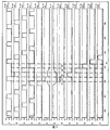
- FIG. 3 is a timing chart showing signals of a shift register unit of the first embodiment of the present invention.
- FIG. 4 shows a cascade diagram of a gate driving circuit of a first embodiment of the present invention
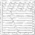
- Figure 6 is a timing chart showing signals when the embodiment of Figure 4 is reverse scanned
- Figure 9 is a circuit configuration diagram of a shift register unit of a third embodiment of the present invention.
- Figure 10 is a circuit configuration diagram of a shift register unit of a fourth embodiment of the present invention.
- the shifting of the signal can be achieved by cascading the shift register units.
- the shift register unit receives the output of the shift register unit of the previous stage as a shift trigger signal of the shift register unit of the stage to output a signal such as a high level in the next period (a period of one half clock period) ).
- the shift register unit can also receive the output of the shift register unit of the next stage as a reset signal of the shift register unit of the stage to resume outputting the low level signal in the next period and subsequent periods.
- the output of the shift register unit of the embodiment of the invention is still provided with a drive level by the clock signal. That is, the clock signal received on the first clock terminal is at a high level in the next period of the period in which the upper stage (forward) or the next stage (reverse) shift register unit outputs a high level (the The "upper level” and “lower level” refer to the “upper level” and “lower level” of the spatially cascading order of the plurality of shift register units when cascading. Since the shift operation period (i.e., one period) of the shift register unit is half a clock cycle, the timing of the clock signal accessed by the first clock terminal of the shift register unit of the adjacent stage should be reversed.
- the first embodiment is a basic implementation circuit of the shift register unit of the present invention, and a basic cascode circuit from which the gate drive circuit is constructed.
- Fig. 2 is a circuit diagram showing a shift register unit of the first embodiment.
- the switching transistors are all "N" type transistors will be described as an example. It is of course possible to implement embodiments of the invention using "P" type transistors.
- the shift register unit may include:
- An input module according to the first clock signal (one of ck4 and ck2), providing the input signal OUT_N-1 to the first node PU (pull-up node);
- a first control module according to the input signal OUT_N-1 and the third clock signal ck1, implementing a pull-up output by providing the third clock signal to an output node OUT_N of the shift register unit, and then according to the input A signal OUT_N+1 is implemented by providing a supply voltage (VGL) to the output node, wherein the input signal OUT_N+1 is used by the input module according to a second clock signal (the other of ck4 and ck2) Provided to the first node PU;
- the second control module maintains the level of the output node at the power supply voltage (VGL) according to the fourth clock signal ck3;
- the first control module includes a first transistor T1, the first transistor T1 continues to be turned on for pull-down output after the pull-up output, and the second control module includes a second transistor T2 for maintaining the The level of the output node.
- the input module may include: a third transistor T3 having a gate connected to the clock signal ck4, a source connected to the input signal OUT_N-1, and a drain connected to the first node PU;
- the transistor T4, the gate of the fourth transistor T4 is connected to the clock signal ck2, the drain is connected to the input signal OUT_N+1, and the source is connected to the first (pull-up) node PU.
- the input signal OUT_N-1 is the output signal of the previous stage of the current stage output signal OUT_N of the shift register unit, and its initial value is STV, for example, the signal SIU in the case of forward shift and the signal SID in the case of reverse shift. .
- the input signal OUT_N+1 is the next-stage output signal of the shift register unit current stage output signal OUT_N.
- the first control module may include: a first transistor T1, the gate of the first transistor T1 is connected to the first node PU, the source is connected to the clock signal ck1, and the drain is connected to the output node OUT_N of the shift register unit; the seventh transistor T7, the gate of the seventh transistor T7 is connected to the first node PU, and one end of the source and the second capacitor C2 is connected at the second node PD (pull-down node), and the drain and the power supply voltage (VGL Connected, the other end of the second capacitor C2 is connected to the power supply voltage (VGL), and the second capacitor C2 is used as a voltage holding capacitor of the second node PD.
- first capacitor C1 and the second capacitor C2 may be inherent parasitic capacitances between transistors, or may be additional additional capacitors.
- the second control module may include: a second transistor T2 having a gate connected to the pull-down node PD, a drain connected to the power supply negative voltage VGL, a source connected to the output node OUT_N, and a fifth transistor T5 a gate and a drain of the fifth transistor T5 are connected to the clock signal ck3, a source is connected to the pull-down node PD, and a gate of the sixth transistor T6, the sixth transistor T6 is connected to the second node (PD), the source The pole is connected to the first node (PU) and the drain is connected to the supply voltage (VGL).
- the shift register unit of this embodiment is controlled by four clock signals ck1-ck4.
- the two-way scanning function can be realized by the third transistor T3 and the fourth transistor T4.
- the conduction of the first transistor T1 can pull down the output point voltage after the output point voltage is pulled up
- the second transistor T2 is a pull-down holding transistor
- the fifth transistor T5 controls the voltage of the pull-down node PD to realize the pulling of the pull-down node PD.
- the sixth transistor T6 controls the voltage of the pull-up node PU. When the PD is high, the PU point is continuously pulled down, the first transistor T1 is turned off, and the seventh transistor T7 is the control transistor of the pull-down node PD.
- the first transistor T1 continues to conduct after the pull-up output, and acts as a pull-down, so that the second transistor T2 is only used to keep the output of the shift register unit low.
- the voltage is such that the output of the shift register unit is controlled only by the first transistor T1. Therefore, the size of the second transistor T2 can be appropriately reduced to facilitate narrow-frame wiring.
- the size ratio of the first transistor T1 and the second transistor T2 is about 30:1 to 1:1, preferably 6:1 to 3:1.
- Fig. 3 shows the signal timing when the shift register unit of the present embodiment performs forward shift. Next, the operation principle of the shift register unit of this embodiment will be described with reference to Figs. 2 and 3.
- ck4 is synchronized with the pulse of the SIU, SIU and ck4 are at a high level, and the remaining clock signals are at a low level.
- the third transistor T3 controlled by ck4 is turned on, and the high level signal of the SIU is transmitted to the gate of the first transistor T1, the first transistor T1 is turned on and charges the first capacitor C1.
- the signal also turns on the seventh transistor T7.
- the second phase (t2): ck1 is high, the remaining clock signals are low, and the SIU signal goes low.
- the voltage Out1 of the output node OUT_N transitions from a low level to a high level.
- the bootstrap effect of the first capacitor C1 pumps the voltage at the PU point high, at which point the first transistor T1 can fully output the high level of ck1 to the output node OUT_N.
- the seventh transistor T7 since the seventh transistor T7 is turned on, the voltage of the pull-down node PD is pulled low.
- the third stage (t3): ck2 is high, the remaining clock signals are low voltage, and the SIU signal is kept low.
- Ck2 is at a high level, and the fourth transistor T4 is turned on. Since the fourth transistor T4 is turned on, the voltage of the pull-up node PU is no longer bootstrapped, but the conduction of the first transistor T1 can still be maintained, and the voltage Out1 of the output node OUT_N transitions from a high level to a low level. Therefore, during the high level of the clock signals ck4, ck1, and ck2, the first transistor T1 is turned on, the voltage point of the pull-down node PD is both low level, and the second transistor T2 is turned off.
- the fourth stage (t4): ck3 is high, the remaining clock signals are low voltage, and the SIU signal is kept low.
- Ck3 is at a high level, and the fifth transistor T5 is turned on, thereby pulling the level of the pull-down node PD high while charging the second capacitor C2, and the second transistor T2 is turned on to maintain the low level of the output node.
- the sixth transistor T6 pulls down the voltage of the pull-up node PU, thereby causing the first transistor T1 to be in an off state.
- the fifth stage (t5): ck4 is high, the remaining clock signals are low voltage, and the SIU signal goes high.
- the third transistor T3 controlled by ck4 is turned on, repeating the above steps of the first stage, thereby starting the operation of the next period of the shift register unit.
- Fig. 4 shows a cascade diagram of the gate driving circuit of the first embodiment.
- the shift register unit of this embodiment constitutes a gate drive circuit in a cascade manner, whereby progressive scanning of each pixel row is realized by shifting of the shift register unit.
- the SIU and SID are the input start pulse signals for the forward and reverse scans, respectively.
- the first input terminal OUT_N-1 of each shift register unit SRn is connected to the upper stage shift register unit SRn-1.
- the output, the first input terminal OUT_N-1 of the first stage shift register unit SR1 is connected to the enable signal SIU; the second input of each shift register unit SRn except the last stage shift register unit SRN OUT_N+1 is connected to the output of the next stage shift register unit SRn+1, and the second input terminal OUT_N+1 of the last stage shift register unit SRN is connected to the enable signal SID.
- the output signal timing of the shift register unit of the subsequent stage is delayed by one cycle from the output signal timing of the shift register unit of the previous stage.
- the clock signals of the shift register units of the adjacent four shift register units satisfy the following relationship:
- the clock signals input to the clock signal input terminals CK1, CK2, CK3, and CK4 are ck1, ck2, ck3, and ck4, respectively;
- the clock signals input to the clock signal input terminals CK1, CK2, CK3, and CK4 are ck2, ck3, ck4, and ck1, respectively;
- the clock signals input to the clock signal input terminals CK1, CK2, CK3, and CK4 are ck3, ck4, ck1, and ck2, respectively;
- the clock signals input to the clock signal input terminals CK1, CK2, CK3, and CK4 are ck4, ck1, ck2, and ck3, respectively.
- the input of the clock signal is the same as the i-th shift register, that is, the clock signals input by the clock signal input terminals CK1, CK2, CK3, and CK4. They are ck1, ck2, ck3, and ck4, and so on.
- i is an integer greater than or equal to 1, and i+3 ⁇ n.
- the input terminal OUT_N-1 receives the output signal OUTi-1 or the turn-on signal SIU from the shift register unit SRn-1 of the upper stage as an enable signal to control The operation of the shift register.
- the input terminal OUT_N+1 receives the output signal OUTi+1 or the turn-on signal SID from the next-stage shift register unit SRn+1 as the enable signal.
- cascaded shift registers can be designed as needed, and can be any level greater than or equal to 2 as long as the clock signals are rotated in the above order.
- the shift register cascade structure of the embodiment only the timings of the control signal and the input signal need to be matched to switch between the forward scan and the reverse scan, and the control signal of the circuit is reduced (other existing shift registers are mostly Two additional directional control signals are required) to facilitate narrow border and high resolution display panel wiring.
- Fig. 5 and Fig. 6 respectively show signal timing charts of the first embodiment at the time of forward shift and reverse shift.
- the signal timing diagram shown in FIG. 5 when the gate driver is forward shifted to forward scan a pixel row is described in conjunction with FIGS. 1 and 4.
- the shift register unit is sequentially referred to as a first-stage shift register unit, a second-stage shift register unit, a third-stage shift register unit, and the fourth stage in order from top to bottom in FIG. a shift register unit and a fifth shift register unit respectively corresponding to the above The i-th i+4th shift register unit.
- the turn-on signal SIU connected to the input terminal OUT_N-1 of the first-stage shift register unit SR1 and the clock signal ck4 connected to the input terminal CK4 are at a high level, other clock signals and signals connected to the input terminal OUT_N+1 To be low, this period is referred to herein as the first period (1 in Fig. 5).
- the third transistor T3 is turned on, and the high level signal of the SIU is transmitted to the gate of the first transistor T1, and the first transistor T1 is turned on, and charges the first capacitor C1.
- the seventh transistor T7 is turned on.
- the voltage of the pull-up node PU is pulled high, and the voltage of the pull-down node PD is slowly pulled down by the PU voltage, and both ends of the second capacitor C2 are at a low level.
- the clock signal ck1 connected to the input terminal CK1 is at a low level, and the voltage Out1 of the output node is at a low level. This period can also be referred to as the current pre-charging period.
- the clock signal ck1 connected to the input terminal CK1 becomes a high level
- the turn-on signal SIU becomes a low level
- the third transistor T3 is turned off
- the pull-up node PU continues to remain high.
- the clock signal ck1 connected to the input terminal CK1 becomes a high level
- the voltage of the output node transitions from a low level to a high level, that is, OUT1 in FIG. 4 outputs a high level.
- the bootstrap effect of the first capacitor C1 pumps the voltage at the PU point high, at which point the first transistor T1 can fully output the high level of the clock signal ck1 to the output node.
- the clock signal ck2 is at a high level, the remaining clock signals are at a low level, and the fourth transistor T4 is turned on. Since the fourth transistor T4 is turned on, the voltage of the pull-up node PU is no longer bootstrapped, but the conduction of the first transistor T1 can be maintained, and the voltage of the output node changes from a high level to a low level.
- This period can be referred to as the local reset period.
- OUT1 input to the input terminal OUT_N-1 of the second-stage shift register unit SR2 is at a low level, and a clock signal ck2 connected to the second-stage input terminal CK1 is at a high level.
- the second-stage shift register unit SR2 the same operation as that of the first-stage shift register unit SR1 in the second period is performed, and OUT2 is a high level, which is the second-stage scanning period.
- the high level OUT2 is input to the input terminal OUT_N-1 of the third stage shift register unit SR3, and the clock signal ck2 connected to the input terminal CK4 of the third stage shift register unit SR3 is at the high level. Therefore, for the third stage shift register unit SR3, the first stage shift register unit SR1 is executed in the first period. The same operation.
- the high level OUT3 is input to the input terminal OUT_N-1 of the fourth stage shift register unit SR4, and the high level clock signal ck3 is connected to the input terminal CK4 of the fourth stage shift register unit SR4. Therefore, for the fourth-stage shift register unit SR4, the same operation as in the first-stage shift register unit SR1 in the first period is performed.
- the access positions of the clock signal ck4 and the clock signal ck2 can be exchanged without changing the input terminal OUT_N-1 and the input terminal OUT_N+. 1 connection relationship.
- the first transistor T1 and the second transistor T2 can precharge the pull-up node PU in a period before the shift register unit performs the line scan, and in the shift register. The cell is discharged to the pull-up node PU at a time period after the cell performs the scan of the line.
- the input terminal OUT_N-1 receives a valid start signal in a period before the current shift register unit performs the scan of the line to control
- the shift register unit of this stage outputs a signal of a high level signal during the current period, and the shift register unit outputs a low level signal after the line scan.
- the timing chart in the reverse scan is shown in FIG. 6 and will not be described here.
- the SIU and SID can be the same signal, and only the timing matching of the corresponding clock control signal needs to be adjusted. It should be noted that when the SIU and the SID are the same signal, if the forward and reverse scans are required to work normally, the clock signals of the first and last stages of the shift register unit circuit must be different, so that the first The phenomenon of the start pulse is input simultaneously in the first stage and the last stage circuit.
- the first embodiment employs a simple circuit that uses only seven transistors and two capacitors to achieve bidirectional shifting. At the same time, when the shift register unit of this stage performs scanning, the pull-up node PU maintains a high voltage due to the bootstrap effect, thereby ensuring the stability of the output.
- the second embodiment is an improvement made on the basis of the first embodiment.
- the cascade manner of the gate driving circuit of this embodiment is the same as that of the first embodiment except for the structure of each shift register unit.
- 7 and 8 show the circuit configuration of the shift register unit of the second embodiment.
- the first embodiment employs a diode connection.
- the drain of the fifth transistor T5 in the second embodiment is connected to the high level VGH.
- the pull-down module of the shift register unit of the second embodiment further includes an eighth transistor T8 and a ninth transistor T9.
- the drain of the eighth transistor T8 is connected to the gate and connected to the clock signal ck2, the source and the pull-down The node PD is connected, the gate of the ninth transistor T9 is connected to the clock signal ck4, the source is connected to the pull-down node PD, and the drain is connected to the power supply positive voltage VGH.
- the input signals of the third transistor T3 and the fourth transistor T4 are interchanged, and the circuit function is unchanged.
- clock signals ck4 and ck2 are respectively input to the gates of the third transistor and the fourth transistor, whereby the PU can be continuously pulled down after the normal output without leakage. If OUT_N-1 and OUT_N+1 are input to the gate and ck2 and ck4 are respectively connected to the source or the drain, there is a risk that the potential of the PU point is pulled high by the leakage of T3 and T4.
- the present invention also provides an image display device including the above-described gate driver.
- the display device may be a liquid crystal display device such as a liquid crystal panel, a liquid crystal television, a mobile phone, an electronic reader, a liquid crystal display, or the like.
Landscapes
- Engineering & Computer Science (AREA)
- Physics & Mathematics (AREA)
- Computer Hardware Design (AREA)
- General Physics & Mathematics (AREA)
- Theoretical Computer Science (AREA)
- Chemical & Material Sciences (AREA)
- Crystallography & Structural Chemistry (AREA)
- Shift Register Type Memory (AREA)
- Liquid Crystal Display Device Control (AREA)
- Control Of Indicators Other Than Cathode Ray Tubes (AREA)
Abstract
Description
Claims (15)
- 一种移位寄存器单元,其特征在于,包括,输入模块,根据第一时钟信号,将第一输入信号提供至第一节点;第一控制模块,与所述输入模块连接于所述第一节点,根据所述第一输入信号和第三时钟信号,通过将所述第三时钟信号提供至所述移位寄存器单元的输出节点来实现上拉输出,并随后根据第二输入信号,通过将电源电压提供至所述输出节点来实现下拉输出,其中所述第二输入信号由所述输入模块根据第二时钟信号提供至所述第一节点;第二控制模块,根据第四时钟信号,将所述输出节点的电平保持在所述电源电压;其中,所述第一控制模块包括第一晶体管,所述第一晶体管在上拉输出后继续导通以进行下拉输出,所述第二控制模块包括第二晶体管,用于保持所述输出节点的电平。
- 如权利要求1所述的移位寄存器单元,其特征在于,所述第一晶体管与所述第二晶体管的尺寸比率为30∶1~1∶1。
- 如权利要求2所述的移位寄存器单元,其特征在于,所述第一晶体管与所述第二晶体管的尺寸比率为6∶1~3∶1。
- 如权利要求2或3所述的移位寄存器单元,其特征在于,所述第一晶体管的栅极与第一节点相连,源极与所述第三时钟信号相连,漏极与所述输出节点相连,在所述第一晶体管的栅极和漏极之间具有第一电容,作为第一节点的电压保持电容;所述第一控制模块还包括第七晶体管,所述第七晶体管的栅极与所述第一节点相连,源极与第二电容的一端在第二节点处相连,漏极与所述电源电压相连,所述第二电容的另一端与所述电源电压相连,所述第二电容用作第二节点的电压保持电容。
- 如权利要求4所述的移位寄存器单元,其特征在于,所述第一电容和第二电容是所述晶体管之间的固有寄生电容,或是附加电容器。
- 如权利要求4所述的移位寄存器单元,其特征在于,所述第二晶体管的栅极连接至所述第二节点,漏极连接至所述电源电压,源极连接至所述输出节点;所述第二控制模块还包括第五晶体管,所述第五晶体管的栅极和漏极连接至所述第四时钟信号,源极与所述第二节点相连;以及第六晶体管,第六晶体管的栅极与所述第二节点相连,源极与第一节点相连,漏极与所述电源电压相连。
- 如权利要求6所述的移位寄存器单元,其特征在于,所述第二控制模块还包括第八晶体管,所述第八晶体管的栅极和漏极连接至所述第二时钟信号,源极与所述第二节点相连;以及第九晶体管,第九晶体管的栅极与所述第一时钟信号相连,源极与所述第二节点相连,漏极与第二电源电压相连,所述第二电源电压与所述电源电压的极性相反。
- 如权利要求4所述的移位寄存器单元,其特征在于,所述第二晶体管的栅极连接至所述第二节点,漏极连接至所述电源电压,源极连接至所述输出节点;所述第二控制模块还包括第五晶体管,所述第五晶体管的栅极连接至所述第四时钟信号,源极与所述第二节点相连,漏极与第二电源电压相连,所述第二电源电压与所述电源电压的极性相反;以及第六晶体管,第六晶体管的栅极与所述第二节点相连,源极与第一节点相连,漏极与所述电源电压相连。
- 如权利要求6-8之一所述的移位寄存器单元,其特征在于,所述输入模块包括:第三晶体管,所述第三晶体管的栅极连接至所述第一时钟信号,源极连接至所述第一输入信号,漏极连接至所述第一节点;以及第四晶体管,所述第四晶体管的栅极连接至所述第四时钟信号,漏极连接至所述第二输入信号,源极连接至所述第一节点。
- 如权利要求6-8之一所述的移位寄存器单元,其特征在于,所述输入模块包括:第三晶体管,所述第三晶体管的栅极连接至所述第一输入信号,源极连接至所述第一时钟信号,漏极连接至所述第一节点;以及第四晶体管,所述第四晶体管的栅极连接至所述第二输入信号,漏极连接至所述第四时钟信号,源极连接至所述第一节点。
- 如权利要求9所述的移位寄存器单元,其特征在于,所述第一晶体管到第九晶体管均为NMOS晶体管,所述电源电压为负电压,所述第二电源电压为正电压。
- 如权利要求10所述的移位寄存器单元,其特征在于,所述第一晶体管到 第九晶体管均为PMOS晶体管,所述电源电压为正电压,所述第二电源电压为负电压。
- 一种栅极驱动电路,其特征在于,包括权利要求1至12中任一项所述的移位寄存器单元。
- 如权利要求13所述的栅极驱动电路,其特征在于,由N个所述移位寄存器单元级联而成,N为大于1的自然数,除了第1级移位寄存器单元之外,每个移位寄存器单元的第一输入端连接上一级移位寄存器单元的输出节点,第1级移位寄存器单元的第一输入端与第一开启信号相连;除了最后1级移位寄存器单元之外,每个移位寄存器单元的第二输入端连接下一级移位寄存器单元的输出节点,最后1级移位寄存器单元的第二输入端与第二开启信号相连;当所述移位寄存器单元进行正向移位时,所述第一时钟信号的高电平脉冲在所述第三时钟信号之前,并且所述第一时钟信号的波形与上一级移位寄存器单元的输出节点的电压波形相同;当所述移位寄存器单元反向移位时,所述第二时钟信号的高电平脉冲在所述第三时钟信号之前,并且所述第二时钟信号的波形与下一级移位寄存器单元的输出节点的电压波形相同。
- 一种显示装置,其特征在于,包括权利要求13或14所述的栅极驱动电路。
Priority Applications (1)
| Application Number | Priority Date | Filing Date | Title |
|---|---|---|---|
| US15/122,265 US10417983B2 (en) | 2015-02-06 | 2015-08-31 | Shift register unit, gate driving circuit and display apparatus |
Applications Claiming Priority (2)
| Application Number | Priority Date | Filing Date | Title |
|---|---|---|---|
| CN201510062488.5A CN104575436B (zh) | 2015-02-06 | 2015-02-06 | 移位寄存器单元、栅极驱动电路及显示装置 |
| CN201510062488.5 | 2015-02-06 |
Publications (1)
| Publication Number | Publication Date |
|---|---|
| WO2016123968A1 true WO2016123968A1 (zh) | 2016-08-11 |
Family
ID=53091350
Family Applications (1)
| Application Number | Title | Priority Date | Filing Date |
|---|---|---|---|
| PCT/CN2015/088646 Ceased WO2016123968A1 (zh) | 2015-02-06 | 2015-08-31 | 移位寄存器单元、栅极驱动电路及显示装置 |
Country Status (3)
| Country | Link |
|---|---|
| US (1) | US10417983B2 (zh) |
| CN (1) | CN104575436B (zh) |
| WO (1) | WO2016123968A1 (zh) |
Cited By (2)
| Publication number | Priority date | Publication date | Assignee | Title |
|---|---|---|---|---|
| CN112992247A (zh) * | 2021-03-05 | 2021-06-18 | 京东方科技集团股份有限公司 | 移位寄存单元、移位寄存器、显示面板及其驱动方法 |
| WO2022188019A1 (zh) * | 2021-03-09 | 2022-09-15 | 京东方科技集团股份有限公司 | 移位寄存器、驱动电路和显示基板 |
Families Citing this family (55)
| Publication number | Priority date | Publication date | Assignee | Title |
|---|---|---|---|---|
| WO2016068038A1 (ja) * | 2014-10-28 | 2016-05-06 | シャープ株式会社 | 単位シフトレジスタ回路、シフトレジスタ回路、単位シフトレジスタ回路の制御方法及び表示装置 |
| CN105895011B (zh) * | 2015-01-26 | 2019-02-15 | 上海和辉光电有限公司 | 移位寄存器单元、栅极驱动电路及显示面板 |
| CN104575396B (zh) * | 2015-02-05 | 2017-07-18 | 京东方科技集团股份有限公司 | 移位寄存器单元及其驱动方法、栅极扫描电路 |
| CN104575436B (zh) | 2015-02-06 | 2017-04-05 | 京东方科技集团股份有限公司 | 移位寄存器单元、栅极驱动电路及显示装置 |
| CN105047120B (zh) * | 2015-06-30 | 2019-01-18 | 上海天马微电子有限公司 | 一种栅极驱动电路及其驱动方法、显示装置 |
| CN104916251B (zh) * | 2015-07-10 | 2018-09-28 | 京东方科技集团股份有限公司 | 栅极驱动电路、触控显示装置和触控显示驱动方法 |
| CN105047155B (zh) | 2015-08-17 | 2017-07-07 | 深圳市华星光电技术有限公司 | 液晶显示装置及其goa扫描电路 |
| CN105118456B (zh) * | 2015-08-31 | 2017-11-03 | 昆山龙腾光电有限公司 | 一种栅极驱动电路及具有该栅极驱动电路的显示装置 |
| CN105185290B (zh) * | 2015-09-06 | 2017-10-10 | 京东方科技集团股份有限公司 | 一种移位寄存器、其驱动方法、栅极驱动电路及显示装置 |
| CN105161134B (zh) * | 2015-10-09 | 2018-10-23 | 京东方科技集团股份有限公司 | 移位寄存器单元及其操作方法、移位寄存器 |
| CN105261340A (zh) * | 2015-11-09 | 2016-01-20 | 武汉华星光电技术有限公司 | Goa驱动电路、tft显示面板及显示装置 |
| CN105374331B (zh) * | 2015-12-01 | 2017-11-17 | 武汉华星光电技术有限公司 | 栅极驱动电路和使用栅极驱动电路的显示器 |
| CN105469754B (zh) * | 2015-12-04 | 2017-12-01 | 武汉华星光电技术有限公司 | 降低馈通电压的goa电路 |
| CN105405406B (zh) * | 2015-12-29 | 2017-12-22 | 武汉华星光电技术有限公司 | 栅极驱动电路和使用栅极驱动电路的显示器 |
| CN105448261B (zh) * | 2015-12-31 | 2018-05-18 | 深圳市华星光电技术有限公司 | 液晶显示器 |
| CN105427825B (zh) | 2016-01-05 | 2018-02-16 | 京东方科技集团股份有限公司 | 一种移位寄存器、其驱动方法及栅极驱动电路 |
| CN105489189B (zh) * | 2016-02-01 | 2018-09-18 | 京东方科技集团股份有限公司 | 栅极驱动单元、栅极驱动电路及其驱动方法和显示装置 |
| CN105575329B (zh) * | 2016-03-16 | 2017-12-01 | 京东方科技集团股份有限公司 | 移位寄存器及驱动方法、驱动电路、阵列基板及显示装置 |
| CN205564251U (zh) * | 2016-04-26 | 2016-09-07 | 北京京东方显示技术有限公司 | 移位寄存器、栅极驱动电路、阵列基板 |
| CN106023919B (zh) * | 2016-06-30 | 2019-01-18 | 京东方科技集团股份有限公司 | 移位寄存器及其驱动方法、驱动电路和显示装置 |
| CN105976751A (zh) * | 2016-07-28 | 2016-09-28 | 武汉华星光电技术有限公司 | 扫描驱动电路及具有该电路的平面显示装置 |
| CN106023936B (zh) * | 2016-07-28 | 2018-10-23 | 武汉华星光电技术有限公司 | 扫描驱动电路及具有该电路的平面显示装置 |
| CN106098002B (zh) * | 2016-08-05 | 2018-10-19 | 武汉华星光电技术有限公司 | 扫描驱动电路及具有该电路的平面显示装置 |
| CN106128379B (zh) * | 2016-08-08 | 2019-01-15 | 武汉华星光电技术有限公司 | Goa电路 |
| CN106531048B (zh) * | 2016-11-29 | 2020-03-27 | 京东方科技集团股份有限公司 | 移位寄存器、栅极驱动电路、显示面板和驱动方法 |
| TWI607450B (zh) * | 2016-12-30 | 2017-12-01 | 友達光電股份有限公司 | 移位暫存器與採用其之閘極驅動電路 |
| CN108630149B (zh) * | 2017-03-22 | 2020-05-05 | 上海和辉光电有限公司 | 显示装置及其移位寄存器 |
| US20180277232A1 (en) * | 2017-03-27 | 2018-09-27 | Int Tech Co., Ltd. | Shift register |
| CN107424552B (zh) * | 2017-06-13 | 2019-11-05 | 京东方科技集团股份有限公司 | 移位寄存器单元、驱动方法、栅极驱动电路和显示装置 |
| TWI616860B (zh) * | 2017-06-27 | 2018-03-01 | 友達光電股份有限公司 | 閘極驅動電路及其運作方法 |
| TWI614757B (zh) * | 2017-07-06 | 2018-02-11 | 友達光電股份有限公司 | 移位暫存器 |
| CN107134271B (zh) * | 2017-07-07 | 2019-08-02 | 深圳市华星光电技术有限公司 | 一种goa驱动电路 |
| CN107657918B (zh) | 2017-09-29 | 2019-10-01 | 上海天马微电子有限公司 | 发光控制信号生成电路、其驱动方法及装置 |
| CN108154860B (zh) * | 2018-01-19 | 2021-02-02 | 昆山龙腾光电股份有限公司 | 一种栅极驱动电路及显示装置 |
| CN108447438B (zh) * | 2018-04-10 | 2020-12-08 | 京东方科技集团股份有限公司 | 显示装置、栅极驱动电路、移位寄存器及其控制方法 |
| CN110503927B (zh) * | 2018-05-16 | 2020-11-10 | 京东方科技集团股份有限公司 | 移位寄存器单元及其驱动方法、栅极驱动电路及显示装置 |
| CN108470535A (zh) * | 2018-06-11 | 2018-08-31 | 京东方科技集团股份有限公司 | 一种移位寄存器、其驱动方法及栅极驱动电路、显示装置 |
| CN110875002B (zh) * | 2018-08-30 | 2021-04-13 | 合肥鑫晟光电科技有限公司 | 栅极驱动单元及其驱动方法、栅极驱动电路、显示装置 |
| CN109686291A (zh) * | 2019-01-22 | 2019-04-26 | 福建华佳彩有限公司 | 一种Notch显示屏的GIP驱动电路及Notch显示屏 |
| CN113454725B (zh) * | 2019-02-12 | 2025-04-18 | 西门子工业软件有限公司 | 用于单路径可逆扫描链的双向扫描单元 |
| CN110223623B (zh) * | 2019-06-18 | 2022-12-16 | 京东方科技集团股份有限公司 | 栅极驱动单元及其控制方法、栅极驱动电路、显示装置 |
| CN110599959B (zh) * | 2019-08-08 | 2020-11-06 | 南京中电熊猫液晶显示科技有限公司 | 触发驱动电路及显示装置 |
| KR102668997B1 (ko) * | 2019-10-21 | 2024-05-24 | 삼성디스플레이 주식회사 | 표시 장치 |
| CN111816123B (zh) | 2020-07-21 | 2022-06-10 | 合肥京东方卓印科技有限公司 | 显示基板及显示装置 |
| CN111816127B (zh) * | 2020-07-27 | 2021-11-16 | Oppo广东移动通信有限公司 | Goa单元及其驱动方法、goa电路和显示面板 |
| CN113077832B (zh) * | 2021-04-30 | 2025-02-07 | 京东方科技集团股份有限公司 | 移位寄存器单元及其驱动方法、扫描驱动电路、显示装置 |
| CN113409717B (zh) * | 2021-05-13 | 2022-06-10 | 北京大学深圳研究生院 | 移位寄存器单元电路,栅极驱动电路及显示器 |
| CN114937431B (zh) * | 2022-05-31 | 2025-09-09 | 惠科股份有限公司 | 扫描驱动电路、显示面板和显示装置 |
| WO2023240513A1 (en) * | 2022-06-15 | 2023-12-21 | Huawei Technologies Co., Ltd. | Shift register, shift register circuit, display panel, and electronic device |
| CN115269491B (zh) * | 2022-07-18 | 2024-03-22 | 北京中科银河芯科技有限公司 | 一种单线通信装置以及单线通信方法 |
| CN115762411B (zh) * | 2022-12-15 | 2026-02-17 | 云谷(固安)科技有限公司 | 栅极驱动电路和显示面板 |
| CN118541804A (zh) * | 2022-12-23 | 2024-08-23 | 京东方科技集团股份有限公司 | 显示基板、制作方法和显示装置 |
| CN119889404B (zh) * | 2023-10-25 | 2026-02-17 | 京东方科技集团股份有限公司 | 一种移位寄存器、栅极驱动电路和显示装置 |
| CN119479576A (zh) * | 2024-12-09 | 2025-02-18 | 上海天马微电子有限公司 | 栅极驱动电路、显示面板与显示装置 |
| CN119541372B (zh) * | 2024-12-27 | 2026-02-27 | 厦门天马光电子有限公司 | 一种阵列基板及包括其的显示面板、显示装置 |
Citations (6)
| Publication number | Priority date | Publication date | Assignee | Title |
|---|---|---|---|---|
| US20060001637A1 (en) * | 2004-06-30 | 2006-01-05 | Sang-Jin Pak | Shift register, display device having the same and method of driving the same |
| CN102419949A (zh) * | 2011-09-02 | 2012-04-18 | 友达光电股份有限公司 | 移位寄存器电路 |
| CN103137061A (zh) * | 2013-02-18 | 2013-06-05 | 京东方科技集团股份有限公司 | 移位寄存器单元、栅极驱动电路及显示装置 |
| CN103956133A (zh) * | 2014-02-13 | 2014-07-30 | 友达光电股份有限公司 | 移位暂存电路及移位暂存器 |
| CN104318886A (zh) * | 2014-10-31 | 2015-01-28 | 京东方科技集团股份有限公司 | 一种goa单元及驱动方法,goa电路和显示装置 |
| CN104575436A (zh) * | 2015-02-06 | 2015-04-29 | 京东方科技集团股份有限公司 | 移位寄存器单元、栅极驱动电路及显示装置 |
Family Cites Families (24)
| Publication number | Priority date | Publication date | Assignee | Title |
|---|---|---|---|---|
| JP4968681B2 (ja) * | 2007-07-17 | 2012-07-04 | Nltテクノロジー株式会社 | 半導体回路とそれを用いた表示装置並びにその駆動方法 |
| US20100067646A1 (en) * | 2008-09-17 | 2010-03-18 | Au Optronics Corporation | Shift register with embedded bidirectional scanning function |
| KR101324410B1 (ko) * | 2009-12-30 | 2013-11-01 | 엘지디스플레이 주식회사 | 쉬프트 레지스터와 이를 이용한 표시장치 |
| CN101783124B (zh) * | 2010-02-08 | 2013-05-08 | 北京大学深圳研究生院 | 栅极驱动电路单元、栅极驱动电路及显示装置 |
| TWI397259B (zh) * | 2010-05-10 | 2013-05-21 | 友達光電股份有限公司 | 移位暫存器電路 |
| TWI433459B (zh) * | 2010-07-08 | 2014-04-01 | Au Optronics Corp | 雙向移位暫存器 |
| CN102637401B (zh) * | 2011-01-25 | 2015-06-24 | 群康科技(深圳)有限公司 | 显示驱动电路与应用其的显示面板 |
| JP5774911B2 (ja) * | 2011-06-01 | 2015-09-09 | 株式会社ジャパンディスプレイ | 表示装置 |
| KR101340197B1 (ko) * | 2011-09-23 | 2013-12-10 | 하이디스 테크놀로지 주식회사 | 쉬프트 레지스터 및 이를 이용한 게이트 구동회로 |
| CN103632641B (zh) * | 2012-08-22 | 2016-01-20 | 瀚宇彩晶股份有限公司 | 液晶显示器及其移位寄存装置 |
| WO2014054518A1 (ja) * | 2012-10-05 | 2014-04-10 | シャープ株式会社 | シフトレジスタ |
| CN102930814A (zh) * | 2012-10-29 | 2013-02-13 | 京东方科技集团股份有限公司 | 移位寄存器及其驱动方法、栅极驱动装置与显示装置 |
| CN103400558B (zh) * | 2013-07-31 | 2015-09-09 | 京东方科技集团股份有限公司 | 移位寄存器单元及其驱动方法、栅极驱动电路及显示装置 |
| CN103714774B (zh) * | 2013-12-19 | 2016-02-17 | 京东方科技集团股份有限公司 | 斜坡信号发生电路及信号发生器、阵列基板及显示装置 |
| CN103714792B (zh) * | 2013-12-20 | 2015-11-11 | 京东方科技集团股份有限公司 | 一种移位寄存器单元、栅极驱动电路及显示装置 |
| CN103700356A (zh) * | 2013-12-27 | 2014-04-02 | 合肥京东方光电科技有限公司 | 移位寄存器单元及其驱动方法、移位寄存器、显示装置 |
| CN104021750B (zh) * | 2014-05-30 | 2016-06-08 | 京东方科技集团股份有限公司 | 移位寄存器单元、栅极驱动电路及驱动方法和显示装置 |
| KR102167138B1 (ko) * | 2014-09-05 | 2020-10-16 | 엘지디스플레이 주식회사 | 쉬프트 레지스터 및 그를 이용한 표시 장치 |
| CN104282255B (zh) * | 2014-09-25 | 2016-09-28 | 京东方科技集团股份有限公司 | 移位寄存器、栅极驱动电路及其驱动方法、显示装置 |
| CN104332146B (zh) * | 2014-11-12 | 2016-09-28 | 合肥鑫晟光电科技有限公司 | 移位寄存器单元、移位寄存器、栅极驱动电路和显示装置 |
| CN105185290B (zh) * | 2015-09-06 | 2017-10-10 | 京东方科技集团股份有限公司 | 一种移位寄存器、其驱动方法、栅极驱动电路及显示装置 |
| CN105336302B (zh) * | 2015-12-07 | 2017-12-01 | 武汉华星光电技术有限公司 | 基于ltps半导体薄膜晶体管的goa电路 |
| CN105355187B (zh) * | 2015-12-22 | 2018-03-06 | 武汉华星光电技术有限公司 | 基于ltps半导体薄膜晶体管的goa电路 |
| CN105489189B (zh) * | 2016-02-01 | 2018-09-18 | 京东方科技集团股份有限公司 | 栅极驱动单元、栅极驱动电路及其驱动方法和显示装置 |
-
2015
- 2015-02-06 CN CN201510062488.5A patent/CN104575436B/zh not_active Expired - Fee Related
- 2015-08-31 US US15/122,265 patent/US10417983B2/en not_active Expired - Fee Related
- 2015-08-31 WO PCT/CN2015/088646 patent/WO2016123968A1/zh not_active Ceased
Patent Citations (6)
| Publication number | Priority date | Publication date | Assignee | Title |
|---|---|---|---|---|
| US20060001637A1 (en) * | 2004-06-30 | 2006-01-05 | Sang-Jin Pak | Shift register, display device having the same and method of driving the same |
| CN102419949A (zh) * | 2011-09-02 | 2012-04-18 | 友达光电股份有限公司 | 移位寄存器电路 |
| CN103137061A (zh) * | 2013-02-18 | 2013-06-05 | 京东方科技集团股份有限公司 | 移位寄存器单元、栅极驱动电路及显示装置 |
| CN103956133A (zh) * | 2014-02-13 | 2014-07-30 | 友达光电股份有限公司 | 移位暂存电路及移位暂存器 |
| CN104318886A (zh) * | 2014-10-31 | 2015-01-28 | 京东方科技集团股份有限公司 | 一种goa单元及驱动方法,goa电路和显示装置 |
| CN104575436A (zh) * | 2015-02-06 | 2015-04-29 | 京东方科技集团股份有限公司 | 移位寄存器单元、栅极驱动电路及显示装置 |
Cited By (4)
| Publication number | Priority date | Publication date | Assignee | Title |
|---|---|---|---|---|
| CN112992247A (zh) * | 2021-03-05 | 2021-06-18 | 京东方科技集团股份有限公司 | 移位寄存单元、移位寄存器、显示面板及其驱动方法 |
| CN112992247B (zh) * | 2021-03-05 | 2024-08-06 | 京东方科技集团股份有限公司 | 移位寄存单元、移位寄存器、显示面板及其驱动方法 |
| WO2022188019A1 (zh) * | 2021-03-09 | 2022-09-15 | 京东方科技集团股份有限公司 | 移位寄存器、驱动电路和显示基板 |
| US12293719B2 (en) | 2021-03-09 | 2025-05-06 | Chengdu Boe Optoelectronics Technology Co., Ltd. | Shift register, driving circuit and display substrate |
Also Published As
| Publication number | Publication date |
|---|---|
| CN104575436A (zh) | 2015-04-29 |
| CN104575436B (zh) | 2017-04-05 |
| US10417983B2 (en) | 2019-09-17 |
| US20160372070A1 (en) | 2016-12-22 |
Similar Documents
| Publication | Publication Date | Title |
|---|---|---|
| WO2016123968A1 (zh) | 移位寄存器单元、栅极驱动电路及显示装置 | |
| US10095058B2 (en) | Shift register and driving method thereof, gate driving device | |
| CN104078017B (zh) | 移位寄存器单元、栅极驱动电路及显示装置 | |
| CN110660362B (zh) | 移位寄存器及栅极驱动电路 | |
| CN105489189B (zh) | 栅极驱动单元、栅极驱动电路及其驱动方法和显示装置 | |
| CN110176204B (zh) | 移位寄存器及其驱动方法、栅极驱动电路、显示装置 | |
| US11227524B2 (en) | Shift register unit and driving method thereof, gate driving circuit and driving method thereof, and display device | |
| CN102982777B (zh) | 显示装置的栅极驱动电路 | |
| CN104299583B (zh) | 一种移位寄存器及其驱动方法、驱动电路和显示装置 | |
| CN105161134B (zh) | 移位寄存器单元及其操作方法、移位寄存器 | |
| US20180335814A1 (en) | Shift register unit, gate drive circuit and display apparatus having the same, and driving method thereof | |
| WO2020015569A1 (zh) | 移位寄存器单元及其驱动方法、栅极驱动电路及显示装置 | |
| US10916171B2 (en) | Gate driver on array circuit and display panel | |
| US20190005866A1 (en) | Shift Register Unit, Driving Method, Gate Driver on Array and Display Device | |
| WO2020024641A1 (zh) | 移位寄存器单元及其驱动方法、栅极驱动电路及显示装置 | |
| US9799262B2 (en) | Shift register and driving method thereof, gate driving circuit | |
| WO2017113984A1 (zh) | 移位寄存器单元及其驱动方法、栅极驱动电路和显示装置 | |
| WO2017020549A1 (zh) | 移位寄存器、栅极驱动电路、显示面板的驱动方法、显示装置 | |
| CN103021358A (zh) | 一种移位寄存器单元、栅极驱动电路及显示器件 | |
| CN104575430A (zh) | 移位寄存器单元及其驱动方法、栅极驱动电路、显示装置 | |
| KR20080081822A (ko) | 시프트 레지스터 회로 및 그것을 구비한 화상표시장치 | |
| CN106652901B (zh) | 驱动电路及使用其的显示装置 | |
| US20200160767A1 (en) | Gate driving circuit, shift register and driving control method thereof | |
| CN103021466A (zh) | 移位寄存器及其工作方法、栅极驱动装置、显示装置 | |
| US10510279B2 (en) | Shift register units, gate scanning circuits, driving methods and display apparatuses |
Legal Events
| Date | Code | Title | Description |
|---|---|---|---|
| WWE | Wipo information: entry into national phase |
Ref document number: 15122265 Country of ref document: US |
|
| 121 | Ep: the epo has been informed by wipo that ep was designated in this application |
Ref document number: 15880915 Country of ref document: EP Kind code of ref document: A1 |
|
| NENP | Non-entry into the national phase |
Ref country code: DE |
|
| 32PN | Ep: public notification in the ep bulletin as address of the adressee cannot be established |
Free format text: CONSTATATION DE LA PERTE D'UN DROIT CONFORMEMENT A LA REGLE 112(1) CBE (OEB FORM 1205N EN DATE DU 30/01/2018) |
|
| 122 | Ep: pct application non-entry in european phase |
Ref document number: 15880915 Country of ref document: EP Kind code of ref document: A1 |