WO2016110891A1 - 太陽電池用基板の製造方法及び太陽電池用基板 - Google Patents
太陽電池用基板の製造方法及び太陽電池用基板 Download PDFInfo
- Publication number
- WO2016110891A1 WO2016110891A1 PCT/JP2015/005846 JP2015005846W WO2016110891A1 WO 2016110891 A1 WO2016110891 A1 WO 2016110891A1 JP 2015005846 W JP2015005846 W JP 2015005846W WO 2016110891 A1 WO2016110891 A1 WO 2016110891A1
- Authority
- WO
- WIPO (PCT)
- Prior art keywords
- substrate
- solar cell
- heat treatment
- temperature heat
- silicon
- Prior art date
- Legal status (The legal status is an assumption and is not a legal conclusion. Google has not performed a legal analysis and makes no representation as to the accuracy of the status listed.)
- Ceased
Links
Images





Classifications
-
- H—ELECTRICITY
- H10—SEMICONDUCTOR DEVICES; ELECTRIC SOLID-STATE DEVICES NOT OTHERWISE PROVIDED FOR
- H10F—INORGANIC SEMICONDUCTOR DEVICES SENSITIVE TO INFRARED RADIATION, LIGHT, ELECTROMAGNETIC RADIATION OF SHORTER WAVELENGTH OR CORPUSCULAR RADIATION
- H10F71/00—Manufacture or treatment of devices covered by this subclass
- H10F71/121—The active layers comprising only Group IV materials
-
- C—CHEMISTRY; METALLURGY
- C30—CRYSTAL GROWTH
- C30B—SINGLE-CRYSTAL GROWTH; UNIDIRECTIONAL SOLIDIFICATION OF EUTECTIC MATERIAL OR UNIDIRECTIONAL DEMIXING OF EUTECTOID MATERIAL; REFINING BY ZONE-MELTING OF MATERIAL; PRODUCTION OF A HOMOGENEOUS POLYCRYSTALLINE MATERIAL WITH DEFINED STRUCTURE; SINGLE CRYSTALS OR HOMOGENEOUS POLYCRYSTALLINE MATERIAL WITH DEFINED STRUCTURE; AFTER-TREATMENT OF SINGLE CRYSTALS OR A HOMOGENEOUS POLYCRYSTALLINE MATERIAL WITH DEFINED STRUCTURE; APPARATUS THEREFOR
- C30B29/00—Single crystals or homogeneous polycrystalline material with defined structure characterised by the material or by their shape
- C30B29/02—Elements
- C30B29/06—Silicon
-
- C—CHEMISTRY; METALLURGY
- C30—CRYSTAL GROWTH
- C30B—SINGLE-CRYSTAL GROWTH; UNIDIRECTIONAL SOLIDIFICATION OF EUTECTIC MATERIAL OR UNIDIRECTIONAL DEMIXING OF EUTECTOID MATERIAL; REFINING BY ZONE-MELTING OF MATERIAL; PRODUCTION OF A HOMOGENEOUS POLYCRYSTALLINE MATERIAL WITH DEFINED STRUCTURE; SINGLE CRYSTALS OR HOMOGENEOUS POLYCRYSTALLINE MATERIAL WITH DEFINED STRUCTURE; AFTER-TREATMENT OF SINGLE CRYSTALS OR A HOMOGENEOUS POLYCRYSTALLINE MATERIAL WITH DEFINED STRUCTURE; APPARATUS THEREFOR
- C30B31/00—Diffusion or doping processes for single crystals or homogeneous polycrystalline material with defined structure; Apparatus therefor
- C30B31/06—Diffusion or doping processes for single crystals or homogeneous polycrystalline material with defined structure; Apparatus therefor by contacting with diffusion material in the gaseous state
- C30B31/08—Diffusion or doping processes for single crystals or homogeneous polycrystalline material with defined structure; Apparatus therefor by contacting with diffusion material in the gaseous state the diffusion materials being a compound of the elements to be diffused
-
- C—CHEMISTRY; METALLURGY
- C30—CRYSTAL GROWTH
- C30B—SINGLE-CRYSTAL GROWTH; UNIDIRECTIONAL SOLIDIFICATION OF EUTECTIC MATERIAL OR UNIDIRECTIONAL DEMIXING OF EUTECTOID MATERIAL; REFINING BY ZONE-MELTING OF MATERIAL; PRODUCTION OF A HOMOGENEOUS POLYCRYSTALLINE MATERIAL WITH DEFINED STRUCTURE; SINGLE CRYSTALS OR HOMOGENEOUS POLYCRYSTALLINE MATERIAL WITH DEFINED STRUCTURE; AFTER-TREATMENT OF SINGLE CRYSTALS OR A HOMOGENEOUS POLYCRYSTALLINE MATERIAL WITH DEFINED STRUCTURE; APPARATUS THEREFOR
- C30B31/00—Diffusion or doping processes for single crystals or homogeneous polycrystalline material with defined structure; Apparatus therefor
- C30B31/06—Diffusion or doping processes for single crystals or homogeneous polycrystalline material with defined structure; Apparatus therefor by contacting with diffusion material in the gaseous state
- C30B31/18—Controlling or regulating
- C30B31/185—Pattern diffusion, e.g. by using masks
-
- C—CHEMISTRY; METALLURGY
- C30—CRYSTAL GROWTH
- C30B—SINGLE-CRYSTAL GROWTH; UNIDIRECTIONAL SOLIDIFICATION OF EUTECTIC MATERIAL OR UNIDIRECTIONAL DEMIXING OF EUTECTOID MATERIAL; REFINING BY ZONE-MELTING OF MATERIAL; PRODUCTION OF A HOMOGENEOUS POLYCRYSTALLINE MATERIAL WITH DEFINED STRUCTURE; SINGLE CRYSTALS OR HOMOGENEOUS POLYCRYSTALLINE MATERIAL WITH DEFINED STRUCTURE; AFTER-TREATMENT OF SINGLE CRYSTALS OR A HOMOGENEOUS POLYCRYSTALLINE MATERIAL WITH DEFINED STRUCTURE; APPARATUS THEREFOR
- C30B33/00—After-treatment of single crystals or homogeneous polycrystalline material with defined structure
- C30B33/02—Heat treatment
-
- H—ELECTRICITY
- H10—SEMICONDUCTOR DEVICES; ELECTRIC SOLID-STATE DEVICES NOT OTHERWISE PROVIDED FOR
- H10F—INORGANIC SEMICONDUCTOR DEVICES SENSITIVE TO INFRARED RADIATION, LIGHT, ELECTROMAGNETIC RADIATION OF SHORTER WAVELENGTH OR CORPUSCULAR RADIATION
- H10F10/00—Individual photovoltaic cells, e.g. solar cells
- H10F10/10—Individual photovoltaic cells, e.g. solar cells having potential barriers
- H10F10/14—Photovoltaic cells having only PN homojunction potential barriers
-
- H—ELECTRICITY
- H10—SEMICONDUCTOR DEVICES; ELECTRIC SOLID-STATE DEVICES NOT OTHERWISE PROVIDED FOR
- H10F—INORGANIC SEMICONDUCTOR DEVICES SENSITIVE TO INFRARED RADIATION, LIGHT, ELECTROMAGNETIC RADIATION OF SHORTER WAVELENGTH OR CORPUSCULAR RADIATION
- H10F71/00—Manufacture or treatment of devices covered by this subclass
- H10F71/128—Annealing
-
- H—ELECTRICITY
- H10—SEMICONDUCTOR DEVICES; ELECTRIC SOLID-STATE DEVICES NOT OTHERWISE PROVIDED FOR
- H10F—INORGANIC SEMICONDUCTOR DEVICES SENSITIVE TO INFRARED RADIATION, LIGHT, ELECTROMAGNETIC RADIATION OF SHORTER WAVELENGTH OR CORPUSCULAR RADIATION
- H10F77/00—Constructional details of devices covered by this subclass
- H10F77/10—Semiconductor bodies
- H10F77/12—Active materials
- H10F77/122—Active materials comprising only Group IV materials
- H10F77/1223—Active materials comprising only Group IV materials characterised by the dopants
-
- H—ELECTRICITY
- H10—SEMICONDUCTOR DEVICES; ELECTRIC SOLID-STATE DEVICES NOT OTHERWISE PROVIDED FOR
- H10P—GENERIC PROCESSES OR APPARATUS FOR THE MANUFACTURE OR TREATMENT OF DEVICES COVERED BY CLASS H10
- H10P32/00—Diffusion of dopants within, into or out of wafers, substrates or parts of devices
-
- H—ELECTRICITY
- H10—SEMICONDUCTOR DEVICES; ELECTRIC SOLID-STATE DEVICES NOT OTHERWISE PROVIDED FOR
- H10P—GENERIC PROCESSES OR APPARATUS FOR THE MANUFACTURE OR TREATMENT OF DEVICES COVERED BY CLASS H10
- H10P95/00—Generic processes or apparatus for manufacture or treatments not covered by the other groups of this subclass
- H10P95/90—Thermal treatments, e.g. annealing or sintering
-
- Y—GENERAL TAGGING OF NEW TECHNOLOGICAL DEVELOPMENTS; GENERAL TAGGING OF CROSS-SECTIONAL TECHNOLOGIES SPANNING OVER SEVERAL SECTIONS OF THE IPC; TECHNICAL SUBJECTS COVERED BY FORMER USPC CROSS-REFERENCE ART COLLECTIONS [XRACs] AND DIGESTS
- Y02—TECHNOLOGIES OR APPLICATIONS FOR MITIGATION OR ADAPTATION AGAINST CLIMATE CHANGE
- Y02E—REDUCTION OF GREENHOUSE GAS [GHG] EMISSIONS, RELATED TO ENERGY GENERATION, TRANSMISSION OR DISTRIBUTION
- Y02E10/00—Energy generation through renewable energy sources
- Y02E10/50—Photovoltaic [PV] energy
- Y02E10/547—Monocrystalline silicon PV cells
-
- Y—GENERAL TAGGING OF NEW TECHNOLOGICAL DEVELOPMENTS; GENERAL TAGGING OF CROSS-SECTIONAL TECHNOLOGIES SPANNING OVER SEVERAL SECTIONS OF THE IPC; TECHNICAL SUBJECTS COVERED BY FORMER USPC CROSS-REFERENCE ART COLLECTIONS [XRACs] AND DIGESTS
- Y02—TECHNOLOGIES OR APPLICATIONS FOR MITIGATION OR ADAPTATION AGAINST CLIMATE CHANGE
- Y02P—CLIMATE CHANGE MITIGATION TECHNOLOGIES IN THE PRODUCTION OR PROCESSING OF GOODS
- Y02P70/00—Climate change mitigation technologies in the production process for final industrial or consumer products
- Y02P70/50—Manufacturing or production processes characterised by the final manufactured product
Definitions
- the present invention relates to a method for manufacturing a solar cell substrate and a solar cell substrate.
- an electrode is formed by a screen printing method using Ag paste as a material, an antireflection film is formed by a CVD method using a SiN x film, and an emitter.
- the layer (n-type diffusion layer) is formed by thermal diffusion (see, for example, Patent Document 1). This thermal diffusion is formed by vapor phase diffusion using POCl 3 or phosphoric acid-based coating diffusion, and heat of about 800 ° C. is applied to the substrate. Furthermore, when a boron diffusion layer is formed as a BSF layer for higher efficiency, it is necessary to apply heat of about 1000 ° C. to the substrate.
- the present invention has been made in view of the above problems, and even when the substrate has a high oxygen concentration, a method for manufacturing a substrate for a solar cell that can suppress a decrease in minority carrier lifetime of the substrate.
- the purpose is to provide.
- the present invention provides a method for manufacturing a substrate for a solar cell made of single crystal silicon, a step of producing a silicon single crystal ingot, and a step of cutting a silicon substrate from the silicon single crystal ingot. And performing a low temperature heat treatment on the silicon substrate at a temperature of 800 ° C. or higher and lower than 1200 ° C., and before performing the low temperature heat treatment, the silicon single crystal ingot or the silicon substrate is heated to 1200 ° C. or higher.
- a method for producing a solar cell substrate characterized by performing a high temperature heat treatment at a temperature of 30 seconds or more.
- the silicon single crystal ingot or the silicon substrate is subjected to a high temperature heat treatment at a temperature of 1200 ° C. or higher for 30 seconds or more, thereby causing oxygen precipitation defects. Since the oxygen-induced defects do not grow even if the oxygen precipitation nuclei that form the basis of this are pre-dissolved and subjected to low-temperature heat treatment in the subsequent manufacturing process, it is possible to manufacture a substrate in which the decrease in minority carrier lifetime is suppressed. Thus, the conversion efficiency of a solar cell manufactured using the manufactured substrate can be improved.
- a heat treatment at a temperature of 800 ° C. or more and less than 1200 ° C. is referred to as a “low temperature heat treatment” in order to distinguish from a “high temperature heat treatment” at a temperature of 1200 ° C. or more for convenience.
- oxygen precipitation nuclei that cause oxygen precipitation defects can be reliably dissolved, so that it is possible to reliably suppress a decrease in minority carrier lifetime of the substrate. .
- the low-temperature heat treatment can be accompanied by dopant diffusion treatment or oxidation treatment.
- the dopant diffusion treatment or the oxidation treatment is often performed within the temperature range of the low-temperature heat treatment.
- the present invention can be suitably applied when performing dopant diffusion treatment or oxidation treatment for performing such low-temperature heat treatment.
- the oxygen concentration of the silicon substrate can be set to 12 ppm or more.
- the oxygen concentration of the silicon substrate is 12 ppm or more
- the conventional method particularly has a large deterioration in the characteristics of the solar cell, and the present invention can be suitably applied.
- the oxygen concentration in the silicon substrate is based on the atomic ratio (in this case, the unit is also written as “ppma”) and is based on the new ASTM standard.
- the silicon single crystal ingot may be doped with phosphorus.
- the present invention can be suitably applied when a silicon single crystal ingot is doped with phosphorus to be n-type.
- the silicon single crystal ingot is preferably doped with gallium, and the time of the high temperature heat treatment is preferably 30 minutes or less.
- gallium as a p-type dopant to be doped into a silicon single crystal ingot, it is possible to more effectively suppress a decrease in minority carrier lifetime of the substrate. Moreover, by setting the time of the high-temperature heat treatment to 30 minutes or less, it is possible to suppress gallium from evaporating from the substrate surface, thereby suppressing the substrate surface from becoming high resistance. The decrease in the fill factor of a solar cell produced using can be suppressed.
- the present invention also provides a solar cell substrate manufactured by the above solar cell substrate manufacturing method.
- Such a solar cell substrate can suppress a decrease in minority carrier lifetime of the substrate, thereby improving the conversion efficiency of a solar cell fabricated using such a substrate.
- substrate for solar cells of this invention As mentioned above, if it is the manufacturing method of the board
- the inventors have intensively studied a method for manufacturing a substrate for a solar cell that can suppress a decrease in minority carrier lifetime of the substrate even when the oxygen concentration of the substrate is high.
- a high temperature heat treatment at a temperature of 1200 ° C. or higher for 30 seconds or more on a silicon single crystal ingot or silicon substrate before performing a low temperature heat treatment of 800 ° C. or higher and lower than 1200 ° C. It is found that oxygen precipitate nuclei to be dissolved in advance and oxygen-induced defects do not grow even after low-temperature heat treatment in the subsequent manufacturing process, so that a substrate in which a decrease in minority carrier lifetime is suppressed can be manufactured.
- the invention Invented the invention.
- a silicon single crystal ingot is manufactured (see step S11 in FIG. 1). Specifically, for example, a silicon single crystal ingot is produced by the CZ method (Czochralski method). At this time, an n-type dopant or a p-type dopant can be doped so that the silicon single crystal ingot has a desired conductivity type. In the growth of the silicon single crystal by the CZ method, oxygen is taken into the silicon single crystal from the quartz crucible containing the raw material melt.
- a silicon substrate is cut out from the silicon single crystal ingot produced in step S11 (see step S12 in FIG. 1). Specifically, for example, a silicon substrate having a predetermined thickness is cut out from a silicon single crystal ingot using a dicing saw, a wire saw, or the like into a wafer shape.
- the silicon substrate cut out in step S12 is subjected to high-temperature heat treatment at a temperature of 1200 ° C. or higher for 30 seconds or longer (see step S13 in FIG. 1).
- the temperature of the high temperature heat treatment means the highest temperature applied to the silicon substrate during the heat treatment
- the time of the high temperature heat treatment means a time for maintaining 1200 ° C. or higher.
- the high-temperature heat treatment can be performed using, for example, a lamp annealer, a horizontal furnace, a vertical furnace, or the like.
- the upper limit of the high temperature heat treatment is in principle the melting point of silicon.
- step S13 a low temperature heat treatment is performed on the silicon substrate at a temperature of 800 ° C. or higher and lower than 1200 ° C. during the process of manufacturing the solar cell substrate (see step S14 in FIG. 1).
- the silicon substrate is subjected to a high temperature heat treatment at a temperature of 1200 ° C. or more for 30 seconds or more to dissolve in advance the oxygen precipitation nuclei that cause oxygen precipitation defects (solid solution). )
- a high temperature heat treatment at a temperature of 1200 ° C. or more for 30 seconds or more to dissolve in advance the oxygen precipitation nuclei that cause oxygen precipitation defects (solid solution).
- oxygen-induced defects do not grow even after low-temperature heat treatment in the subsequent manufacturing process, so that it is possible to manufacture a substrate in which a decrease in minority carrier lifetime is suppressed, thereby using the manufactured substrate.
- the conversion efficiency of the produced solar cell can be improved.
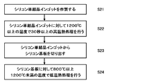
- a silicon single crystal ingot is manufactured (see step S21 in FIG. 2).
- step S21 the silicon single crystal ingot produced in step S21 is subjected to high-temperature heat treatment for 30 seconds or more at a temperature of 1200 ° C. or higher (see step S22 in FIG. 2).
- a silicon substrate is cut out from the silicon single crystal ingot subjected to the high temperature heat treatment (see step S23 in FIG. 2).
- low-temperature heat treatment is performed on the silicon substrate at a temperature of 800 ° C. or higher and lower than 1200 ° C. (see step S24 in FIG. 2).
- a high temperature heat treatment can be performed on the silicon single crystal ingot.
- the low-temperature heat treatment can be accompanied by a dopant diffusion treatment or an oxidation treatment.
- the dopant diffusion treatment or the oxidation treatment is often performed by the low-temperature heat treatment.
- the present invention can be suitably applied when dopant diffusion treatment or oxidation treatment for performing such low-temperature heat treatment is performed as the low-temperature heat treatment in the present invention.
- the oxygen concentration of the silicon substrate can be 12 ppm (12 ppma, new ASTM standard) or more.
- the present invention can be suitably applied when the oxygen concentration of the silicon substrate is 12 ppm or more.
- the oxygen concentration tends to be high, and tends to be 12 ppm or more.
- the oxygen concentration tends to be high at the initial stage of pulling the CZ crystal (cone side).
- a silicon substrate having a high oxygen concentration can be obtained without excluding the silicon substrate.
- the silicon single crystal ingot can be doped with phosphorus.
- the present invention can be suitably applied when a silicon single crystal ingot is doped with phosphorus to be n-type.
- the silicon single crystal ingot is doped with gallium and the time of the high-temperature heat treatment is 30 minutes or less.
- gallium as a p-type dopant for doping a silicon single crystal ingot, it is possible to more effectively suppress a decrease in minority carrier lifetime of the substrate.
- time of the high-temperature heat treatment it is possible to suppress gallium from evaporating from the substrate surface, thereby suppressing the substrate surface from becoming high resistance. The decrease in the fill factor of a solar cell produced using can be suppressed.
- the high-temperature heat treatment in an atmosphere containing phosphorus oxychloride. If high-temperature heat treatment is performed in an atmosphere containing phosphorus oxychloride, a decrease in minority carrier lifetime of the substrate can be more effectively suppressed due to the strong gettering action of phosphorus.
- Phosphorus is doped in an atmosphere containing this phosphorus oxychloride, but this is not a problem.
- a phosphorus-doped substrate is originally doped with phosphorus.
- an n-type dopant is introduced anyway when forming a pn junction.
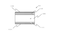
- the solar cell substrate 10 in FIG. 3 is manufactured using the solar cell substrate manufacturing method described above with reference to FIGS. 1 and 2.
- the solar cell substrate 10 is provided on, for example, a phosphorus-doped silicon substrate 100, an emitter layer (boron diffusion layer) 110 provided on the light-receiving surface side of the phosphorus-doped silicon substrate 100, and a back surface side of the phosphorus-doped silicon substrate 100.
- a light-receiving surface antireflection film 120 is provided on the light-receiving surface side surface of the emitter layer 110, and a back-surface antireflection film 121 is provided on the back surface side of the BSF layer 111. Is provided.
- the solar cell substrate 10 is manufactured by performing a high temperature heat treatment at a temperature of 1200 ° C. or higher for 30 seconds or more on a silicon single crystal ingot or a silicon substrate before performing a low temperature heat treatment of 800 ° C. or higher and lower than 1200 ° C. Is. For this reason, oxygen precipitation nuclei that cause oxygen precipitation defects are dissolved in advance, and oxygen-induced defects do not grow even after low-temperature heat treatment in the subsequent manufacturing process.
- the low temperature heat treatment here is, for example, a boron diffusion heat treatment for forming the emitter layer 110.
- the solar cell substrate 10 is a substrate in which a decrease in minority carrier lifetime is suppressed, whereby the conversion efficiency of a solar cell manufactured using such a substrate can be improved. .
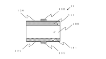
- a light receiving surface electrode 130 is provided on the light receiving surface side surface of the emitter layer 110 of the solar cell substrate 10, and a back electrode 131 is formed on the back surface side of the BSF layer 111 of the solar cell substrate 10. Is provided.
- the light receiving surface electrode 130 penetrates the light receiving surface antireflection film 120 and is electrically connected to the emitter layer 110, and the back electrode 131 penetrates the back surface antireflection film 121.
- the BSF layer 111 is electrically connected.
- FIG. 3 an example of a method for manufacturing the solar cell substrate 10 of FIG. 3 (an embodiment using a phosphorus-doped substrate) will be specifically described with reference to FIG.
- the present invention is not limited to the following method for manufacturing a solar cell substrate.
- cleaning is performed after removing the damaged layer of the phosphorus-doped silicon substrate 100 cut out from the silicon single crystal ingot (see FIG. 5A).
- the damage layer can be removed, for example, by immersing the phosphorus-doped silicon substrate 100 in a hot concentrated potassium hydroxide aqueous solution.
- the phosphorus-doped silicon substrate 100 from which the damaged layer has been removed is subjected to a high-temperature heat treatment at a temperature of 1200 ° C. or higher for 30 seconds or longer (see FIG. 5B).
- the high-temperature heat treatment can be performed using, for example, a lamp annealer, a horizontal furnace, a vertical furnace, or the like.
- the phosphorus-doped silicon substrate 100 subjected to the high-temperature heat treatment is subjected to texture etching and then cleaned (see FIG. 5C).
- Texture etching can be performed, for example, by dipping in an aqueous solution of potassium hydroxide / 2-propanol. By performing texture etching, fine unevenness called texture can be formed, and the reflectance of the light receiving surface can be reduced.
- This texture forming process can also be performed before the high temperature heat treatment. In this case, the high-temperature heat treatment and the subsequent diffusion mask formation step can be continuously performed using a horizontal furnace or the like.
- a diffusion mask for forming the emitter layer 110 is formed on the phosphorus-doped silicon substrate 100 subjected to texture etching (see FIG. 5D).
- the diffusion mask can be formed, for example, by placing the phosphorus-doped silicon substrate 100 in a horizontal furnace, growing an oxide film by thermal oxidation, and etching the oxide film on one side.
- the oxidation is performed by wet oxidation, which is faster than dry oxidation, and preferably by pyro-oxidation.
- This thermal oxidation treatment may be performed within the temperature range of “low temperature heat treatment”.
- boron diffusion is performed on the phosphorus-doped silicon substrate 100 on which the diffusion mask is formed (see FIG. 5E).
- Boron diffusion can be performed, for example, by placing the phosphorus-doped silicon substrate 100 in a horizontal furnace and performing a heat treatment in an argon and BBr 3 gas atmosphere. By this step, an emitter layer (boron diffusion layer) 110 is formed.
- This heat treatment is performed, for example, at a temperature of about 1000 ° C. (within the temperature range of “low temperature heat treatment”).
- a diffusion mask for forming the BSF layer 111 is formed on the phosphorus-doped silicon substrate 100 subjected to boron diffusion (see FIG. 5G).
- the diffusion mask can be formed by putting the substrate 100 on which the emitter is formed in a horizontal furnace, growing an oxide film by thermal oxidation, and etching the oxide film on the back side. This thermal oxidation treatment may also be performed within the temperature range of “low temperature heat treatment”.
- phosphorus diffusion is performed on the phosphorus-doped silicon substrate 100 on which the diffusion mask is formed (see FIG. 5H).
- Phosphorus diffusion can be performed, for example, by placing the phosphorus-doped silicon substrate 100 in a horizontal furnace and performing a heat treatment in an oxygen and POCl 3 gas atmosphere. By this step, a BSF layer (phosphorus diffusion layer) 111 is formed. In the phosphorus diffusion using POCl 3 , heat of about 800 ° C. is usually applied to the substrate.
- a passivation film such as an oxide film or an aluminum oxide film may be formed on the surface of the phosphorus-doped silicon substrate 100 in order to increase the conversion efficiency.
- the passivation film can be formed on the oxide film by thermal oxidation, LPCVD, or the like.
- the aluminum oxide film can be formed by PECVD, ALD, or the like.
- a light-receiving surface antireflection film 120 is formed on the light-receiving surface side surface of the emitter layer 110 of the phosphorus-doped silicon substrate 100 (see FIG. 5 (j)).
- the light-receiving surface antireflection film 120 can be formed, for example, by forming a silicon nitride film by plasma CVD.
- a back surface antireflection film 121 is formed on the light receiving surface side surface of the BSF layer 111 of the phosphorus-doped silicon substrate 100 (see FIG. 5 (k)).
- the back surface antireflection film 121 can be formed, for example, by forming a silicon nitride film by plasma CVD.
- the solar cell substrate 10 of FIG. 3 can be manufactured.
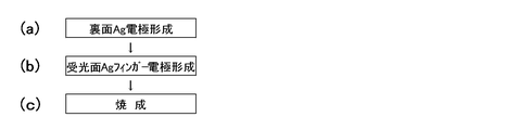
- a back electrode 131 is formed on the back surface of the back surface antireflection film 121 of the solar cell substrate 10 (see FIG. 6A).
- the back electrode 131 can be formed, for example, by screen printing in a desired pattern using a silver paste.
- a light receiving surface electrode 130 is formed on the light receiving surface side surface of the light receiving surface antireflection film 120 of the solar cell substrate 10 (see FIG. 6B).
- the formation of the light receiving surface electrode 130 can be performed, for example, by screen printing in a desired pattern using a silver paste.
- the firing temperature is, for example, 600 to 850 ° C.
- the light-receiving surface electrode 130, the emitter layer 110, and the light-receiving surface electrode 130 and the back-surface anti-reflection film 121 are not opened, and these films are passed through the back-surface electrode 131 and the light-receiving surface electrode 130 during firing.
- the back electrode 131 and the BSF layer 111 can be electrically connected.
- the solar cell substrate 20 includes, for example, a gallium-doped silicon substrate 101 and an emitter layer (phosphorus diffusion layer) 112 provided on the light-receiving surface side of the gallium-doped silicon substrate 101.
- the light-receiving surface of the emitter layer 112 A light-receiving surface antireflection film 120 is provided on the side surface.
- the solar cell substrate 20 is manufactured by performing a high-temperature heat treatment at a temperature of 1200 ° C. or more for 30 seconds or more on a silicon single crystal ingot or a silicon substrate before performing a low-temperature heat treatment at 800 ° C. or more and less than 1200 ° C. Is. For this reason, oxygen precipitation nuclei that cause oxygen precipitation defects are dissolved in advance, and oxygen-induced defects do not grow even after low-temperature heat treatment in the subsequent manufacturing process.
- the low temperature heat treatment here is, for example, phosphorus diffusion heat treatment for forming the emitter layer 112.
- the solar cell substrate 20 is a substrate in which the decrease in minority carrier lifetime is suppressed in this way, and thereby the conversion efficiency of a solar cell manufactured using such a substrate can be improved.
- a light receiving surface electrode 130 is provided on the light receiving surface side surface of the emitter layer 112 of the solar cell substrate 20, and a back surface aluminum electrode 132 is provided on the back surface side surface of the solar cell substrate 20.
- a BSF layer (aluminum diffusion layer) 113 is provided on the back side of the solar cell substrate 20.
- the light receiving surface electrode 130 penetrates the light receiving surface antireflection film 120 and is electrically connected to the emitter layer 112, and the back surface aluminum electrode 132 is electrically connected to the BSF layer 113. It is connected.
- cleaning is performed after removing the damaged layer of the gallium-doped silicon substrate 101 cut out from the silicon single crystal ingot (see FIG. 9A).
- the gallium-doped silicon substrate 101 from which the damaged layer has been removed is subjected to a high-temperature heat treatment at a temperature of 1200 ° C. or higher for 30 seconds or longer (see FIG. 9B).
- the gallium-doped silicon substrate 101 that has been subjected to the high-temperature heat treatment is subjected to texture etching and then cleaned (see FIG. 9C).
- This texture forming step may be performed before or after the high temperature heat treatment step.
- a diffusion mask for forming the emitter layer 112 is formed on the gallium-doped silicon substrate 101 subjected to texture etching (see FIG. 9D).
- the diffusion mask can be formed by placing the gallium-doped silicon substrate 101 in a horizontal furnace, growing an oxide film by thermal oxidation, and etching one side.
- Phosphorus diffusion is performed on the gallium-doped silicon substrate 101 on which the diffusion mask is formed (see FIG. 9E).
- Phosphorus diffusion can be performed, for example, by placing the gallium-doped silicon substrate 101 in a horizontal furnace and performing a heat treatment in an oxygen and POCl 3 gas atmosphere.
- two gallium-doped silicon substrates 101 are placed in one groove of a quartz boat during diffusion, and POCl 3 gas does not flow around on one side, It is also possible to form a phosphorus diffusion layer.
- the heat treatment temperature at this time is usually around 800 ° C.
- a light-receiving surface antireflection film 120 is formed on the light-receiving surface side surface of the emitter layer 112 of the gallium-doped silicon substrate 101 (see FIG. 9G).
- the light-receiving surface antireflection film 120 can be formed, for example, by forming a silicon nitride film by plasma CVD.
- the solar cell substrate 20 of FIG. 7 can be manufactured.
- the back surface aluminum electrode 132 is formed in addition to the bus bar electrode portion on the back surface side surface of the solar cell substrate 20 (see FIG. 10A).
- the back surface aluminum electrode 132 can be formed by, for example, screen printing an Al paste on the back surface of the solar cell substrate 20.
- a silver electrode can be formed by screen printing using a silver paste on the bus bar electrode portion on the back surface of the solar cell substrate 20 (see FIG. 10B).
- the light receiving surface electrode 130 is formed on the light receiving surface side surface of the light receiving surface antireflection film 120 of the solar cell substrate 20 (see FIG. 10C).
- baking is performed on the solar cell substrate 20 on which the back surface aluminum electrode 132 and the light receiving surface electrode 130 are formed (see FIG. 10D).
- aluminum diffuses from the back surface aluminum electrode 132 into the gallium-doped silicon substrate 101, and a BSF layer (aluminum diffusion layer) 113 is formed.
- the light-receiving surface electrode 130 and the emitter layer 112 can be electrically connected by passing the film through the light-receiving surface electrode 130 during firing without opening the light-receiving surface antireflection film 120.
- Example 1 The solar cell substrate 10 of FIG. 3 was manufactured according to the manufacturing flow of FIG. However, the phosphorus-doped silicon substrate 100 is an n-type substrate having a resistivity of 1 ⁇ ⁇ cm (CZ method pulled, oxygen concentration 17 to 18 ppm), and high-temperature heat treatment is performed in a horizontal furnace (using a SiC tube) in a nitrogen atmosphere. The test was performed at 1250 ° C. for 5 minutes.
- FIG. 11A shows an EL (electroluminescence) image after manufacturing the solar cell. It can be seen from FIG. 11A that the spiral oxygen-induced defects described later have disappeared. Moreover, about the manufactured solar cell, the characteristics (short circuit current density, open circuit voltage, fill factor, conversion efficiency) of the solar cell were measured. The results are shown in Table 1.
- the short-circuit current density is the current density value when the resistance of the resistor connected to the solar cell is 0 ⁇
- the open circuit voltage is the voltage when the resistance of the resistor connected to the solar cell is very large.
- the fill factor shape factor
- the conversion efficiency is (output from the solar cell / solar energy entering the solar cell) ⁇ 100.
- Example 2 The solar cell substrate 10 of FIG. 3 was produced in the same manner as in Example 1. However, high-temperature heat treatment is performed by phosphorus diffusion in a horizontal furnace (using a SiC tube) in a POCl 3 atmosphere at 1200 ° C. for 10 minutes, thereby dissolving oxygen precipitation nuclei and ring gettering (gettering by phosphorus). went.
- Example 1 The solar cell substrate 10 of FIG. 3 was produced in the same manner as in Example 1. However, high temperature heat treatment was not performed.
- FIG. 11B shows an EL image after manufacturing the solar cell. It can be seen from FIG. 11B that spiral oxygen-induced defects are observed. Moreover, about the manufactured solar cell, the characteristics (short circuit current density, open circuit voltage, fill factor, conversion efficiency) of the solar cell were measured. The results are shown in Table 1.
- Example 1-2 when a phosphorus-doped substrate is used, the conversion efficiency is improved in Example 1-2 as compared with Comparative Example 1. Further, in Example 1-2, variations in characteristics (short-circuit current density, open-circuit voltage, fill factor, conversion efficiency) of the solar cell are reduced as compared with Comparative Example 1. This is because in Example 1-2 in which high-temperature heat treatment was performed, the generation of oxygen-induced defects was suppressed as compared with Comparative Example 1 in which high-temperature heat treatment was not performed (see FIG. 11). This is probably because the lifetime of the bulk portion is suppressed from decreasing. Furthermore, it can be seen that in Example 2 where the high-temperature heat treatment was performed in a POCl 3 atmosphere, the conversion efficiency was further improved.
- the solar cell substrate 20 of FIG. 7 was manufactured according to the manufacturing flow of FIG.
- the gallium-doped silicon substrate 101 is a p-type substrate having a resistivity of 1 ⁇ ⁇ cm (CZ method pulled, oxygen concentration 17-18 ppm), and high-temperature heat treatment is performed in a horizontal furnace (using a SiC tube) in a nitrogen atmosphere. The test was performed at 1250 ° C. for 5 minutes.
- Example 4 In the same manner as in Example 3, the solar cell substrate 20 of FIG. 7 was manufactured. However, in the high temperature heat treatment, phosphorus diffusion was performed in a horizontal furnace (using a SiC tube) in a POCl 3 atmosphere at 1200 ° C. for 10 minutes, thereby dissolving oxygen precipitation nuclei and performing a ring getter.
- Example 5 In the same manner as in Example 3, the solar cell substrate 20 of FIG. 7 was manufactured. However, the high temperature heat treatment was performed in a horizontal furnace (using a SiC tube) in a nitrogen atmosphere at 1250 ° C. for 40 minutes.
- Example 3-5 As can be seen from Table 2, the conversion efficiency is improved in Example 3-5 as compared with Comparative Example 2 even when the gallium doped substrate is used. Further, in Example 3-5, variations in characteristics (short-circuit current density, open-circuit voltage, fill factor, conversion efficiency) of the solar cell are reduced as compared with Comparative Example 2. This is because in Example 3-5 in which high-temperature heat treatment was performed, the generation of oxygen-induced defects was suppressed as compared with Comparative Example 2 in which high-temperature heat treatment was not performed, thereby reducing the lifetime of the bulk portion of the substrate. This is thought to be because the decrease was suppressed. Furthermore, it can be seen that in Example 4 where the high-temperature heat treatment was performed in a POCl 3 atmosphere, the conversion efficiency was further improved.
- Example 3-4 in which the high temperature heat treatment is 30 minutes or less, the fill factor and the conversion efficiency are improved as compared with Example 5 in which the high temperature heat treatment exceeds 30 minutes.
- the high-temperature heat treatment is set to 30 minutes or less to prevent the gallium dopant from escaping from the substrate, and the warpage prevents the substrate from increasing in resistance and increasing the series resistance. This is probably because of this.
- the present invention is not limited to the above embodiment.
- the above-described embodiment is an exemplification, and the present invention has substantially the same configuration as the technical idea described in the claims of the present invention, and any device that exhibits the same function and effect is the present invention. It is included in the technical scope of the invention.
Landscapes
- Chemical & Material Sciences (AREA)
- Crystallography & Structural Chemistry (AREA)
- Engineering & Computer Science (AREA)
- Materials Engineering (AREA)
- Metallurgy (AREA)
- Organic Chemistry (AREA)
- Physics & Mathematics (AREA)
- Thermal Sciences (AREA)
- Photovoltaic Devices (AREA)
- Life Sciences & Earth Sciences (AREA)
- Sustainable Development (AREA)
- Formation Of Insulating Films (AREA)
Abstract
本発明は、単結晶シリコンからなる太陽電池用基板の製造方法であって、シリコン単結晶インゴットを作製する工程と、前記シリコン単結晶インゴットからシリコン基板を切り出す工程と、前記シリコン基板に対して800℃以上1200℃未満の温度で低温熱処理を行う工程とを有し、前記低温熱処理を行う前に、前記シリコン単結晶インゴット又は前記シリコン基板に対して1200℃以上の温度で30秒以上の高温熱処理を行うことを特徴とする太陽電池用基板の製造方法である。これにより、基板の酸素濃度が多い場合であっても、基板のライフタイムの低下を抑制することができる太陽電池用基板の製造方法が提供される。
Description
本発明は、太陽電池用基板の製造方法及び太陽電池用基板に関する。
一般的な太陽電池は、p型シリコン基板を用いる場合には、電極はAgペーストを材料としたスクリーン印刷法により形成され、また、反射防止膜はSiNx膜をCVD法により形成され、さらにエミッタ層(n型拡散層)は熱拡散により形成されている(例えば、特許文献1を参照)。この熱拡散はPOCl3による気相拡散、もしくはリン酸ベースの塗布拡散で形成しており、800℃前後の熱が基板に加わる。さらに、高効率化のためBSF層としてボロン拡散層を形成する場合には、1000℃前後の熱を基板に加える必要がある。
しかしながら、上記したような熱拡散や、基板表面に酸化膜を形成する際に800℃以上のような熱処理がシリコン単結晶基板に加えられると、シリコン単結晶基板にある濃度以上の酸素原子が含まれていた場合、酸素に起因する欠陥が成長し、シリコン単結晶基板の少数キャリアライフタイムが低下する場合があった。また、その結果、このような基板を用いて作製された太陽電池の特性が低下するという問題があった。上記の特性低下は特に酸素濃度の高い基板で顕著であった。
本発明は、上記問題点に鑑みてなされたものであって、基板の酸素濃度が多い場合であっても、基板の少数キャリアライフタイムの低下を抑制することができる太陽電池用基板の製造方法を提供することを目的とする。
上記目的を達成するために、本発明は、単結晶シリコンからなる太陽電池用基板の製造方法であって、シリコン単結晶インゴットを作製する工程と、前記シリコン単結晶インゴットからシリコン基板を切り出す工程と、前記シリコン基板に対して800℃以上1200℃未満の温度で低温熱処理を行う工程とを有し、前記低温熱処理を行う前に、前記シリコン単結晶インゴット又は前記シリコン基板に対して1200℃以上の温度で30秒以上の高温熱処理を行うことを特徴とする太陽電池用基板の製造方法を提供する。
このように、800℃以上1200℃未満の温度の低温熱処理を行う前に、シリコン単結晶インゴット又はシリコン基板に対して1200℃以上の温度で30秒以上の高温熱処理を行うことで、酸素析出欠陥のもとになる酸素析出核を予め溶かし、後続の製造プロセスにおいて低温熱処理を経ても、酸素起因欠陥が成長しないので、少数キャリアライフタイムの低下が抑制された基板を製造することができ、それによって、製造された基板を用いて作製した太陽電池の変換効率を向上させることができる。本発明の説明では、便宜上1200℃以上の温度の「高温熱処理」と区別するために、800℃以上1200℃未満の温度の熱処理を、「低温熱処理」と称する。
このとき、前記シリコン単結晶インゴットから前記シリコン基板を切り出した後に、前記シリコン基板に対して前記高温熱処理を行うことが好ましい。
このようにシリコン基板に対して高温熱処理を行えば、酸素析出欠陥のもとになる酸素析出核を確実に溶かすことができるので、基板の少数キャリアライフタイムの低下を確実に抑制することができる。
このとき、前記低温熱処理を、ドーパント拡散処理、又は、酸化処理に伴うものとすることができる。
太陽電池用基板の製造において、ドーパント拡散処理、又は、酸化処理は上記低温熱処理の温度範囲で行うことが多い。このような低温熱処理を行うドーパント拡散処理、又は、酸化処理を行う場合に、本発明を好適に適用することができる。
このとき、前記シリコン基板の酸素濃度を12ppm以上とすることができる。
シリコン基板の酸素濃度が12ppm以上である場合には、従来法では特に太陽電池の特性の低下が大きく、本発明を好適に適用することができる。なお、本発明の説明において、シリコン基板中の酸素濃度は原子数比基準(この場合、単位を「ppma」とも書く)であり、new ASTM規格に基づくものである。
このとき、シリコン単結晶インゴットをリンでドープされているものとすることができる。
シリコン単結晶インゴットがリンでドープされてn型になっている場合に、本発明を好適に適用することができる。
このとき、前記シリコン単結晶インゴットをガリウムでドープされているものとし、前記高温熱処理の時間を30分以下とすることが好ましい。
シリコン単結晶インゴットにドーピングするp型ドーパントとして、ガリウムを用いることにより、基板の少数キャリアライフタイムの低下をより効果的に抑制することができる。また、高温熱処理の時間を30分以下とすることで、基板表面からガリウムが蒸発することを抑制でき、これにより、基板の表面が高抵抗になることを抑制することができ、このような基板を用いて作製した太陽電池のフィルファクタの低下を抑制することができる。
このとき、高温熱処理をオキシ塩化リンを含む雰囲気下で行うことが好ましい。
高温熱処理をオキシ塩化リンを含む雰囲気下で行えば、リンの強力なゲッタリング作用により、基板の少数キャリアライフタイムの低下をより効果的に抑制することができる。
また、本発明は、上記の太陽電池用基板の製造方法により製造されたものであることを特徴とする太陽電池用基板を提供する。
このような太陽電池用基板であれば、基板の少数キャリアライフタイムの低下を抑制することができ、それによって、このような基板を用いて作製した太陽電池の変換効率を向上させることができる。
以上のように、本発明の太陽電池用基板の製造方法であれば、少数キャリアライフタイムの低下が抑制された基板を製造することができ、それによって、製造された基板を用いて作製した太陽電池の変換効率を向上させることができる。また、本発明の太陽電池用基板であれば、基板の少数キャリアライフタイムの低下を抑制することができ、それによって、このような基板を用いて作製した太陽電池の変換効率を向上させることができる。
以下、本発明について、実施態様の一例として、図を参照しながら詳細に説明するが、本発明はこれに限定されるものではない。
前述したように、800℃以上1200℃未満のような熱処理がシリコン単結晶基板に加えられると、シリコン単結晶基板にある濃度以上の酸素原子が含まれていた場合、酸素に起因する欠陥が成長し、シリコン単結晶基板の少数キャリアライフタイムが低下し、その結果、このような基板を用いて作製された太陽電池の特性が低下するという問題があった。
そこで、発明者らは、基板の酸素濃度が高い場合であっても、基板の少数キャリアライフタイムの低下を抑制することができる太陽電池用基板の製造方法について鋭意検討を重ねた。その結果、800℃以上1200℃未満の低温熱処理を行う前に、シリコン単結晶インゴット又はシリコン基板に対して1200℃以上の温度で30秒以上の高温熱処理を行うことで、酸素析出欠陥のもとになる酸素析出核を予め溶かし、後続の製造プロセスにおいて低温熱処理を経ても、酸素起因欠陥が成長しないことによって、少数キャリアライフタイムの低下が抑制された基板を製造することができることを見出し、本発明をなすに至った。
以下、図1を参照しながら、本発明の太陽電池用基板の製造方法の実施態様の一例(第1の態様)を説明する。
まず、シリコン単結晶インゴットを作製する(図1のステップS11を参照)。具体的には、例えば、CZ法(チョクラルスキー法)によりシリコン単結晶インゴットを作製する。このとき、シリコン単結晶インゴットが所望の導電型を有するように、n型ドーパント、又はp型ドーパントをドーピングすることができる。なお、CZ法によるシリコン単結晶の育成において、原料融液を収容する石英ルツボから酸素がシリコン単結晶中に取り込まれる。
次に、ステップS11で作製したシリコン単結晶インゴットからシリコン基板を切り出す(図1のステップS12を参照)。具体的には、例えば、ダイシングソー、ワイヤーソー等を用いて、シリコン単結晶インゴットから、所定の厚さを有するシリコン基板をウェーハ状に切り出す。
次に、ステップS12で切り出したシリコン基板に対して1200℃以上の温度で30秒以上の高温熱処理を行う(図1のステップS13を参照)。ここで、高温熱処理の温度とは、熱処理中にシリコン基板に加わる最高温度を意味し、高温熱処理の時間とは、1200℃以上を維持する時間を意味する。なお、高温熱処理は、例えば、ランプアニーラー、横型炉、縦型炉等を用いて行うことができる。高温熱処理の上限は、原理的に、シリコンの融点である。
ステップS13の後に、太陽電池用基板を製造するプロセス中において、シリコン基板に対して800℃以上1200℃未満の低温熱処理を行う(図1のステップS14を参照)。
このように、低温熱処理を行う前に、シリコン基板に対して1200℃以上の温度で30秒以上の高温熱処理を行うことで、酸素析出欠陥のもとになる酸素析出核を予め溶かす(固溶させる)。これにより、後続の製造プロセスにおいて低温熱処理を経ても、酸素起因欠陥が成長しないので、少数キャリアライフタイムの低下が抑制された基板を製造することができ、それによって、製造された基板を用いて作製した太陽電池の変換効率を向上させることができる。
次に、図2を参照しながら、本発明の太陽電池用基板の製造方法の実施態様の他の例(第2の態様)を説明する。第1の態様と重複する説明は適宜省略する。
まず、シリコン単結晶インゴットを作製する(図2のステップS21を参照)。
次に、ステップS21で作製したシリコン単結晶インゴットに対して、1200℃以上の温度で30秒以上の高温熱処理を行う(図2のステップS22を参照)。
次に、高温熱処理を行ったシリコン単結晶インゴットからシリコン基板を切り出す(図2のステップS23を参照)。
次に、太陽電池用基板を製造するプロセスにおいて、シリコン基板に対して800℃以上1200℃未満の低温熱処理を行う(図2のステップS24を参照)。
図2を用いて上記で説明したように、本発明ではシリコン単結晶インゴットに対して高温熱処理を行うこともできる。
上記の第1の態様、第2の態様ともに、低温熱処理を、ドーパント拡散処理、又は、酸化処理に伴うものとすることができる。太陽電池用基板の製造において、ドーパント拡散処理、又は、酸化処理は上記低温熱処理で行うことが多い。このような低温熱処理を行うドーパント拡散処理、又は、酸化処理を本発明における低温熱処理として行う場合に、本発明を好適に適用することができる。
ここで、シリコン基板の酸素濃度を12ppm(12ppma、new ASTM規格)以上とすることができる。シリコン基板の酸素濃度を12ppm以上である場合に、本発明を好適に適用することができる。特に、CZ法でシリコン単結晶インゴット(CZ結晶)を作製し、該インゴットからシリコン基板を切り出すときは、酸素濃度が高くなりやすく、12ppm以上となりやすい。特にCZ結晶の引上げ初期(コーン側)は酸素濃度が高くなりやすい。このように酸素濃度が一本のシリコン単結晶インゴットの位置によってバラツキがある場合であっても、酸素濃度が高いシリコン基板を除外せずに、太陽電池用基板とすることができる。
ここで、シリコン単結晶インゴットをリンでドープされているものとすることができる。シリコン単結晶インゴットがリンでドープされてn型になっている場合に、本発明を好適に適用することができる。
ここで、シリコン単結晶インゴットをガリウムでドープされているものとし、前記高温熱処理の時間を30分以下とすることが好ましい。シリコン単結晶インゴットにドーピングするp型ドーパントとして、ガリウムを用いることにより、基板の少数キャリアライフタイムの低下をより効果的に抑制することができる。また、高温熱処理の時間を30分以下とすることで、基板表面からガリウムが蒸発することを抑制でき、これにより、基板の表面が高抵抗になることを抑制することができ、このような基板を用いて作製した太陽電池のフィルファクタの低下を抑制することができる。
ここで、高温熱処理をオキシ塩化リンを含む雰囲気下で行うことが好ましい。高温熱処理をオキシ塩化リンを含む雰囲気下で行えば、リンの強力なゲッタリング作用により、基板の少数キャリアライフタイムの低下をより効果的に抑制することができる。このオキシ塩化リンを含む雰囲気下でリンがドープされることになるが、これは問題とならない。例えば、リンドープ基板であれば元々リンがドープされているからである。また、ガリウムドープ基板であれば、pn接合を形成する際にいずれにしろn型ドーパントを導入するからである。
次に、図3を参照しながら、本発明の太陽電池用基板の実施態様の一例を説明する。
図3の太陽電池用基板10は、上記で図1及び図2を用いて説明した太陽電池用基板の製造方法を用いて製造されたものである。太陽電池用基板10は、例えば、リンドープシリコン基板100と、リンドープシリコン基板100の受光面側に設けられたエミッタ層(ボロン拡散層)110と、リンドープシリコン基板100の裏面側に設けられたBSF層(リン拡散層)111を有しており、エミッタ層110の受光面側表面には受光面反射防止膜120が設けられ、BSF層111の裏面側表面には裏面反射防止膜121が設けられている。
太陽電池用基板10は、800℃以上1200℃未満の低温熱処理を行う前に、シリコン単結晶インゴット又はシリコン基板に対して1200℃以上の温度で30秒以上の高温熱処理を行って製造されているものである。そのため、酸素析出欠陥のもとになる酸素析出核を予め溶かされており、後続の製造プロセスにおいて低温熱処理を経ても、酸素起因欠陥が成長しない。ここでの低温熱処理とは、例えば、エミッタ層110を形成するためのボロン拡散熱処理である。太陽電池用基板10は、このように、少数キャリアライフタイムの低下が抑制された基板となっており、それによって、このような基板を用いて作製した太陽電池の変換効率を向上させることができる。
次に、図4を参照しながら、太陽電池用基板10を用いて製造した太陽電池の実施態様の一例を説明する。
図4の太陽電池11は、太陽電池用基板10のエミッタ層110の受光面側表面上に受光面電極130が設けられ、太陽電池用基板10のBSF層111の裏面側表面上に裏面電極131が設けられたものである。なお、図4では、太陽電池11において、受光面電極130は受光面反射防止膜120を貫通してエミッタ層110と電気的に接続されており、裏面電極131は裏面反射防止膜121を貫通してBSF層111と電気的に接続されている例を示している。
次に、図5を参照しながら、図3の太陽電池用基板10の製造方法の一例(リンドープ基板を用いた態様)を具体的に説明する。本発明は、以下の太陽電池用基板の製造方法に限定されない。
まず、シリコン単結晶インゴットから切り出したリンドープシリコン基板100のダメージ層を除去してから洗浄を行う(図5(a)を参照)。ダメージ層の除去は、例えば、リンドープシリコン基板100を熱濃水酸化カリウム水溶液中に浸漬することで行うことができる。
次に、ダメージ層が除去されたリンドープシリコン基板100に対して、1200℃以上の温度で30秒以上の高温熱処理を行う(図5(b)を参照)。ここで、高温熱処理は、例えば、ランプアニーラー、横型炉、縦型炉等を用いて行うことができる。
次に、高温熱処理を行ったリンドープシリコン基板100に対してテクスチャエッチングを行ってから洗浄を行う(図5(c)を参照)。テクスチャエッチングは、例えば、水酸化カリウム/2-プロパノールの水溶液中に浸漬することで行うことができる。なお、テクスチャエッチングを行うことでテクスチャと呼ばれる微細な凹凸を形成することができ、受光面の反射率を低減することができる。なお、このテクスチャ形成処理は前記高温熱処理の前に行うことも可能である。この場合、高温熱処理と次工程の拡散マスク形成工程は、横型炉等を用いて、連続的に行うことも可能である。
次に、テクスチャエッチングを行ったリンドープシリコン基板100に対してエミッタ層110形成用の拡散マスクを形成する(図5(d)を参照)。拡散マスクの形成は、例えば、リンドープシリコン基板100を横型炉に入れ、熱酸化により酸化膜を成長させ、片面の酸化膜をエッチングすることで行うことができる。この際、酸化はドライ酸化より酸化膜成長の早いウェット酸化、好ましくはパイロ酸化で行うことがコストの面からも好適である。この熱酸化処理は、「低温熱処理」の温度範囲内で行ってもよい。
次に、拡散マスクを形成したリンドープシリコン基板100に対してボロン拡散を行う(図5(e)を参照)。ボロン拡散は、例えば、リンドープシリコン基板100を横型炉に入れ、アルゴンおよびBBr3ガス雰囲気の中で熱処理することで行うことができる。この工程により、エミッタ層(ボロン拡散層)110が形成される。この熱処理は、例えば、1000℃程度の温度(「低温熱処理」の温度範囲内)で行われる。
次に、リンドープシリコン基板100の表面に形成されたボロンガラスおよび酸化珪素膜をふっ酸で除去する(図5(f)を参照)。
次に、ボロン拡散を行ったリンドープシリコン基板100に対してBSF層111形成用の拡散マスクを形成する(図5(g)を参照)。拡散マスクの形成は、エミッタを形成した基板100を横型炉に入れ、熱酸化により酸化膜を成長させ、裏面側の酸化膜をエッチングすることで行うことができる。この熱酸化処理も「低温熱処理」の温度範囲内で行うことがある。
次に、拡散マスクを形成したリンドープシリコン基板100に対してリン拡散を行う(図5(h)を参照)。リン拡散は、例えば、リンドープシリコン基板100を横型炉に入れ、酸素およびPOCl3ガス雰囲気の中で熱処理することで行うことができる。この工程により、BSF層(リン拡散層)111が形成される。このPOCl3を用いたリン拡散は、通常800℃前後の熱が基板に加わる。
次に、リンドープシリコン基板100の表面に形成されたリンガラスおよび酸化珪素膜をふっ酸で除去する(図5(i)を参照)。さらに、変換効率を高めるために、リンドープシリコン基板100の表面に酸化膜や酸化アルミ膜のパッシベーション膜を形成しても良い。このパッシベーション膜の形成は酸化膜に対しては、熱酸化、LPCVD等により形成することが可能である。また、酸化アルミ膜に対しては、PECVD、ALD等により形成可能である。
次に、リンドープシリコン基板100のエミッタ層110の受光面側表面に受光面反射防止膜120を形成する(図5(j)を参照)。受光面反射防止膜120の形成は、例えば、プラズマCVDにより窒化珪素膜を形成することで行うことができる。
次に、リンドープシリコン基板100のBSF層111の受光面側表面に裏面反射防止膜121を形成する(図5(k)を参照)。裏面反射防止膜121の形成は、例えば、プラズマCVDにより窒化珪素膜を形成することで行うことができる。
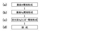
上記のようにして、図3の太陽電池用基板10を製造することができる。
次に、図6を参照しながら、図3の太陽電池用基板10を用いて図4の太陽電池11を製造する方法の一例を説明する。
まず、太陽電池用基板10の裏面反射防止膜121の裏面側表面に裏面電極131を形成する(図6(a)を参照)。裏面電極131の形成は、例えば、銀ペーストを用いて所望のパターンにスクリーン印刷することで行うことができる。
次に、太陽電池用基板10の受光面反射防止膜120の受光面側表面に受光面電極130を形成する(図6(b)を参照)。受光面電極130の形成は、例えば、銀ペーストを用いて所望のパターンにスクリーン印刷することで行うことができる。
次に、裏面電極131及び受光面電極130の形成を行った太陽電池用基板10に対して焼成を行う(図6(c)を参照)。この焼成の際の温度は、例えば、600~850℃である。なお、受光面反射防止膜120及び裏面反射防止膜121を開口せずに、焼成時に裏面電極131及び受光面電極130にこれらの膜を貫通させることにより、受光面電極130とエミッタ層110、及び、裏面電極131とBSF層111を電気的に接続させることができる。
上記のようにして、図4の太陽電池11を製造することができる。
次に、図7を参照しながら、本発明の太陽電池用基板の実施態様の他の例を説明する。
図7の太陽電池用基板20は、上記で図1及び図2を用いて説明した太陽電池用基板の製造方法を用いて製造されたものである。太陽電池用基板20は、例えば、ガリウムドープシリコン基板101と、ガリウムドープシリコン基板101の受光面側に設けられたエミッタ層(リン拡散層)112とを有しており、エミッタ層112の受光面側表面には受光面反射防止膜120が設けられている。
太陽電池用基板20は、800℃以上1200℃未満の低温熱処理を行う前に、シリコン単結晶インゴット又はシリコン基板に対して1200℃以上の温度で30秒以上の高温熱処理を行って製造されているものである。そのため、酸素析出欠陥のもとになる酸素析出核を予め溶かされており、後続の製造プロセスにおいて低温熱処理を経ても、酸素起因欠陥が成長しない。ここでの低温熱処理とは、例えば、エミッタ層112を形成するためのリン拡散熱処理である。太陽電池用基板20は、このように少数キャリアライフタイムの低下が抑制された基板となっており、それによって、このような基板を用いて製造した太陽電池の変換効率を向上させることができる。
次に、図8を参照しながら、太陽電池用基板20を用いて製造した太陽電池の実施態様の他の例を説明する。
図8の太陽電池21は、太陽電池用基板20のエミッタ層112の受光面側表面上に受光面電極130が設けられ、太陽電池用基板20の裏面側表面に裏面アルミニウム電極132が設けられ、太陽電池用基板20の裏面側にBSF層(アルミニウム拡散層)113が設けられたものである。なお、図8では、太陽電池21において、受光面電極130は受光面反射防止膜120を貫通してエミッタ層112と電気的に接続されており、裏面アルミニウム電極132はBSF層113と電気的に接続されている。
次に、図9を参照しながら、図7の太陽電池用基板20の製造方法の一例(ガリウムドープ基板を用いた態様)を具体的に説明する。既に説明したリンドープ基板を用いる態様と重複する説明は適宜省略する。
まず、シリコン単結晶インゴットから切り出したガリウムドープシリコン基板101のダメージ層を除去してから洗浄を行う(図9(a)を参照)。
次に、ダメージ層が除去されたガリウムドープシリコン基板101に対して、1200℃以上の温度で30秒以上の高温熱処理を行う(図9(b)を参照)。
次に、高温熱処理を行ったガリウムドープシリコン基板101に対してテクスチャエッチングを行ってから洗浄を行う(図9(c)を参照)。本テクスチャ形成工程は前記高温熱処理工程と前後しても構わない。
次に、テクスチャエッチングを行ったガリウムドープシリコン基板101に対してエミッタ層112形成用の拡散マスクを形成する(図9(d)を参照)。拡散マスクの形成は、ガリウムドープシリコン基板101を横型炉に入れ、熱酸化により酸化膜を成長させ、片面をエッチングすることで行うことができる。
次に、拡散マスクを形成したガリウムドープシリコン基板101に対してリン拡散を行う(図9(e)を参照)。リン拡散は、例えば、ガリウムドープシリコン基板101を横型炉に入れ、酸素およびPOCl3ガス雰囲気の中で熱処理することで行うことができる。製造コストを低減するために、前記拡散マスクを形成せず、拡散時にガリウムドープシリコン基板101を石英ボートの一溝に2枚入れ、片面にPOCl3ガスが回り込まないようにして、他方の片面にリン拡散層を形成することも可能である。このときの熱処理温度は、通常、800℃前後である。
次に、ガリウムドープシリコン基板101の表面に形成されたリンガラスおよび酸化珪素膜をふっ酸で除去する(図9(f)を参照)。
次に、ガリウムドープシリコン基板101のエミッタ層112の受光面側表面に受光面反射防止膜120を形成する(図9(g)を参照)。受光面反射防止膜120の形成は、例えば、プラズマCVDにより窒化珪素膜を形成することで行うことができる。
上記のようにして、図7の太陽電池用基板20を製造することができる。
次に、図10を参照しながら、図7の太陽電池用基板20を用いて図8の太陽電池21を製造する方法の一例を説明する。
まず、太陽電池用基板20の裏面側表面のバスバー電極部以外に裏面アルミニウム電極132を形成する(図10(a)を参照)。裏面アルミニウム電極132の形成は、例えば、Alペーストを太陽電池用基板20の裏面にスクリーン印刷することで行うことができる。
次に、太陽電池用基板20の裏面のバスバー電極部に銀ペーストを用いて、スクリーン印刷により銀電極を形成することができる(図10(b)を参照)。
次に、太陽電池用基板20の受光面反射防止膜120の受光面側表面に受光面電極130を形成する(図10(c)を参照)。
次に、裏面アルミニウム電極132、及び受光面電極130の形成を行った太陽電池用基板20に対して焼成を行う(図10(d)を参照)。この焼成時に、裏面アルミニウム電極132からアルミニウムがガリウムドープシリコン基板101内に拡散し、BSF層(アルミニウム拡散層)113が形成される。なお、受光面反射防止膜120を開口せずに、焼成時に受光面電極130にこの膜を貫通させることにより、受光面電極130とエミッタ層112を電気的に接続させることができる。
上記のようにして、図8の太陽電池21を製造することができる。
以下、実施例及び比較例を示して本発明をより具体的に説明するが、本発明はこれらの実施例に限定されるものではない。
(実施例1)
図3の太陽電池用基板10を図5の製造フローで製造した。ただし、リンドープシリコン基板100は、n型で抵抗率1Ω・cmの基板(CZ法引き上げ、酸素濃度17~18ppm)を用い、高温熱処理は、横型炉(SiCチューブを使用)で窒素雰囲気下、1250℃、5分の条件で行った。
図3の太陽電池用基板10を図5の製造フローで製造した。ただし、リンドープシリコン基板100は、n型で抵抗率1Ω・cmの基板(CZ法引き上げ、酸素濃度17~18ppm)を用い、高温熱処理は、横型炉(SiCチューブを使用)で窒素雰囲気下、1250℃、5分の条件で行った。
製造した太陽電池用基板を用いて、図6の製造フローで図4の太陽電池11を100枚製造した。太陽電池製造後のEL(エレクトロルミネッセンス)画像を図11(a)に示す。図11(a)より後述する渦巻き状の酸素起因欠陥が消滅していることがわかる。また、製造した太陽電池について、太陽電池の特性(短絡電流密度、開放電圧、フィルファクタ、変換効率)を測定した。その結果を表1に示す。ここで、短絡電流密度は、太陽電池に接続される抵抗器の抵抗が0Ωの時の電流密度値であり、開放電圧は、太陽電池に接続される抵抗器の抵抗が非常に大きい時の電圧値であり、フィルファクタ(形状因子)は、最大発電電力/(短絡電流×開放電圧)であり、変換効率は、(太陽電池からの出力/太陽電池に入った太陽エネルギー)×100である。
(実施例2)
実施例1と同様にして、図3の太陽電池用基板10を製造した。ただし、高温熱処理は、横型炉(SiCチューブを使用)でPOCl3雰囲気下、1200℃、10分の条件でリン拡散を行い、これにより酸素析出核を溶かすとともにリンゲッター(リンによるゲッタリング)を行った。
実施例1と同様にして、図3の太陽電池用基板10を製造した。ただし、高温熱処理は、横型炉(SiCチューブを使用)でPOCl3雰囲気下、1200℃、10分の条件でリン拡散を行い、これにより酸素析出核を溶かすとともにリンゲッター(リンによるゲッタリング)を行った。
製造した太陽電池用基板を用いて、実施例1と同様にして、図4の太陽電池11を100枚製造した。製造した太陽電池について、太陽電池の特性(短絡電流密度、開放電圧、フィルファクタ、変換効率)を測定した。その結果を表1に示す。
(比較例1)
実施例1と同様にして、図3の太陽電池用基板10を製造した。ただし、高温熱処理は行わなかった。
実施例1と同様にして、図3の太陽電池用基板10を製造した。ただし、高温熱処理は行わなかった。
製造した太陽電池用基板を用いて、実施例1と同様にして、図4の太陽電池11を100枚製造した。太陽電池製造後のEL画像を図11(b)に示す。図11(b)より渦巻き状の酸素起因欠陥が見られることがわかる。また、製造した太陽電池について、太陽電池の特性(短絡電流密度、開放電圧、フィルファクタ、変換効率)を測定した。その結果を表1に示す。

表1からわかるように、リンドープ基板を用いた場合、実施例1-2では、比較例1と比べて変換効率が向上していることがわかる。また、実施例1-2では、比較例1と比べて太陽電池の特性(短絡電流密度、開放電圧、フィルファクタ、変換効率)のばらつきが低減されている。これは、高温熱処理を行っている実施例1-2では、高温熱処理を行っていない比較例1と比べて、酸素起因欠陥の生成が抑制されていて(図11を参照)、これにより基板のバルク部分のライフタイムの低下を抑制させているためと考えられる。さらに、高温熱処理をPOCl3雰囲気下で行った実施例2では、変換効率がより向上していることがわかる。
(実施例3)
図7の太陽電池用基板20を図9の製造フローで製造した。ただし、ガリウムドープシリコン基板101は、p型で抵抗率1Ω・cmの基板(CZ法引き上げ、酸素濃度17~18ppm)を用い、高温熱処理は、横型炉(SiCチューブを使用)で窒素雰囲気下、1250℃、5分の条件で行った。
図7の太陽電池用基板20を図9の製造フローで製造した。ただし、ガリウムドープシリコン基板101は、p型で抵抗率1Ω・cmの基板(CZ法引き上げ、酸素濃度17~18ppm)を用い、高温熱処理は、横型炉(SiCチューブを使用)で窒素雰囲気下、1250℃、5分の条件で行った。
製造した太陽電池用基板を用いて、図10の製造フローで図8の太陽電池21を100枚製造した。製造した太陽電池について、太陽電池の特性(短絡電流密度、開放電圧、フィルファクタ、変換効率)を測定した。その結果を表2に示す。
(実施例4)
実施例3と同様にして、図7の太陽電池用基板20を製造した。ただし、高温熱処理は、横型炉(SiCチューブを使用)でPOCl3雰囲気下、1200℃、10分の条件でリン拡散を行い、これにより酸素析出核を溶かすとともにリンゲッターを行った。
実施例3と同様にして、図7の太陽電池用基板20を製造した。ただし、高温熱処理は、横型炉(SiCチューブを使用)でPOCl3雰囲気下、1200℃、10分の条件でリン拡散を行い、これにより酸素析出核を溶かすとともにリンゲッターを行った。
製造した太陽電池用基板を用いて、実施例3と同様にして、図8の太陽電池21を100枚製造した。製造した太陽電池について、太陽電池の特性(短絡電流密度、開放電圧、フィルファクタ、変換効率)を測定した。その結果を表2に示す。
(比較例2)
実施例3と同様にして、図7の太陽電池用基板20を製造した。ただし、高温熱処理は行わなかった。
実施例3と同様にして、図7の太陽電池用基板20を製造した。ただし、高温熱処理は行わなかった。
製造した太陽電池用基板を用いて、実施例3と同様にして、図8の太陽電池21を100枚製造した。製造した太陽電池について、太陽電池の特性(短絡電流密度、開放電圧、フィルファクタ、変換効率)を測定した。その結果を表2に示す。
(実施例5)
実施例3と同様にして、図7の太陽電池用基板20を製造した。ただし、高温熱処理は、横型炉(SiCチューブを使用)で窒素雰囲気下、1250℃、40分の条件で行った。
実施例3と同様にして、図7の太陽電池用基板20を製造した。ただし、高温熱処理は、横型炉(SiCチューブを使用)で窒素雰囲気下、1250℃、40分の条件で行った。
製造した太陽電池用基板を用いて、実施例3と同様にして、図8の太陽電池21を100枚製造した。製造した太陽電池について、太陽電池の特性(短絡電流密度、開放電圧、フィルファクタ、変換効率)を測定した。その結果を表2に示す。

表2からわかるように、ガリウムドープ基板を用いた場合も、実施例3-5では、比較例2と比べて変換効率が向上していることがわかる。また、実施例3-5では、比較例2と比べて太陽電池の特性(短絡電流密度、開放電圧、フィルファクタ、変換効率)のばらつきが低減されている。これは、高温熱処理を行っている実施例3-5では、高温熱処理を行っていない比較例2と比べて、酸素起因欠陥の生成が抑制されていて、これにより基板のバルク部分のライフタイムの低下を抑制させているためと考えられる。さらに、高温熱処理をPOCl3雰囲気下で行った実施例4では、変換効率がより向上していることがわかる。また、高温熱処理を30分以下としている実施例3-4では、高温熱処理が30分を超えている実施例5と比較して、フィルファクタ、変換効率が向上している。これは、実施例3-4では、高温熱処理を30分以下とすることで基板からガリウムドーパントが抜けることを防止し、そりにより、基板が高抵抗化し直列抵抗が増大することを防止しているためと考えられる。
なお、本発明は、上記実施形態に限定されるものではない。上記実施形態は、例示であり、本発明の特許請求の範囲に記載された技術的思想と実質的に同一な構成を有し、同様な作用効果を奏するものは、いかなるものであっても本発明の技術的範囲に包含される。
Claims (8)
- 単結晶シリコンからなる太陽電池用基板の製造方法であって、
シリコン単結晶インゴットを作製する工程と、
前記シリコン単結晶インゴットからシリコン基板を切り出す工程と、
前記シリコン基板に対して800℃以上1200℃未満の温度で低温熱処理を行う工程とを有し、
前記低温熱処理を行う前に、前記シリコン単結晶インゴット又は前記シリコン基板に対して1200℃以上の温度で30秒以上の高温熱処理を行うことを特徴とする太陽電池用基板の製造方法。 - 前記シリコン単結晶インゴットから前記シリコン基板を切り出した後に、前記シリコン基板に対して前記高温熱処理を行うことを特徴とする請求項1に記載の太陽電池用基板の製造方法。
- 前記低温熱処理が、ドーパント拡散処理、又は、酸化処理に伴うものであることを特徴とする請求項1又は請求項2に記載の太陽電池用基板の製造方法。
- 前記シリコン基板の酸素濃度を12ppm以上とすることを特徴とする請求項1から請求項3のいずれか一項に記載の太陽電池用基板の製造方法。
- 前記シリコン単結晶インゴットをリンでドープされているものとすることを特徴とする請求項1から請求項4のいずれか一項に記載の太陽電池用基板の製造方法。
- 前記シリコン単結晶インゴットをガリウムでドープされているものとし、前記高温熱処理の時間を30分以下とすることを特徴とする請求項1から請求項4のいずれか一項に記載の太陽電池用基板の製造方法。
- 前記高温熱処理をオキシ塩化リンを含む雰囲気下で行うことを特徴とする請求項1から請求項6のいずれか一項に記載の太陽電池用基板の製造方法。
- 請求項1から請求項7のいずれか一項に記載の太陽電池用基板の製造方法により製造されたものであることを特徴とする太陽電池用基板。
Priority Applications (5)
| Application Number | Priority Date | Filing Date | Title |
|---|---|---|---|
| DE112015005529.0T DE112015005529T5 (de) | 2015-01-05 | 2015-11-25 | Verfahren zur Herstellung eines Substrats für eine Solarzelle und Substrat für eine Solarzelle |
| US15/538,893 US11901475B2 (en) | 2015-01-05 | 2015-11-25 | Method for manufacturing substrate for solar cell and substrate for solar cell |
| CN201580072513.6A CN107148681A (zh) | 2015-01-05 | 2015-11-25 | 太阳能电池用基板的制造方法及太阳能电池用基板 |
| US16/732,954 US12414401B2 (en) | 2015-01-05 | 2020-01-02 | Method for manufacturing substrate for solar cell and substrate for solar cell |
| US18/521,384 US12237435B2 (en) | 2015-01-05 | 2023-11-28 | Method for manufacturing substrate for solar cell and substrate for solar cell |
Applications Claiming Priority (2)
| Application Number | Priority Date | Filing Date | Title |
|---|---|---|---|
| JP2015000554A JP5938113B1 (ja) | 2015-01-05 | 2015-01-05 | 太陽電池用基板の製造方法 |
| JP2015-000554 | 2015-01-05 |
Related Child Applications (3)
| Application Number | Title | Priority Date | Filing Date |
|---|---|---|---|
| US15/538,893 A-371-Of-International US11901475B2 (en) | 2015-01-05 | 2015-11-25 | Method for manufacturing substrate for solar cell and substrate for solar cell |
| US16/732,954 Division US12414401B2 (en) | 2015-01-05 | 2020-01-02 | Method for manufacturing substrate for solar cell and substrate for solar cell |
| US18/521,384 Division US12237435B2 (en) | 2015-01-05 | 2023-11-28 | Method for manufacturing substrate for solar cell and substrate for solar cell |
Publications (1)
| Publication Number | Publication Date |
|---|---|
| WO2016110891A1 true WO2016110891A1 (ja) | 2016-07-14 |
Family
ID=56184701
Family Applications (1)
| Application Number | Title | Priority Date | Filing Date |
|---|---|---|---|
| PCT/JP2015/005846 Ceased WO2016110891A1 (ja) | 2015-01-05 | 2015-11-25 | 太陽電池用基板の製造方法及び太陽電池用基板 |
Country Status (6)
| Country | Link |
|---|---|
| US (3) | US11901475B2 (ja) |
| JP (1) | JP5938113B1 (ja) |
| CN (3) | CN111092128A (ja) |
| DE (1) | DE112015005529T5 (ja) |
| TW (1) | TWI587539B (ja) |
| WO (1) | WO2016110891A1 (ja) |
Families Citing this family (6)
| Publication number | Priority date | Publication date | Assignee | Title |
|---|---|---|---|---|
| KR101816186B1 (ko) * | 2016-09-01 | 2018-01-08 | 엘지전자 주식회사 | 태양 전지의 제조 방법 |
| CN106671301A (zh) * | 2016-12-07 | 2017-05-17 | 安徽爱森能源有限公司 | 一种开方后硅块的截断方法 |
| CN111584679A (zh) * | 2020-04-07 | 2020-08-25 | 国家电投集团西安太阳能电力有限公司 | 一种用于N型TOPCon电池背表面钝化的掺杂方法 |
| CN112909130A (zh) * | 2021-03-17 | 2021-06-04 | 苏州联诺太阳能科技有限公司 | 一种太阳能电池片的制备方法 |
| CN115036398B (zh) * | 2022-05-13 | 2025-04-15 | 浙江晶盛光子科技有限公司 | 一种p型硅的太阳能电池的制备方法 |
| MY208894A (en) * | 2023-08-08 | 2025-06-06 | Zhuhai Fushan Aiko Solar Tech Co Ltd | Solar cell |
Citations (4)
| Publication number | Priority date | Publication date | Assignee | Title |
|---|---|---|---|---|
| JPH05206146A (ja) * | 1992-01-24 | 1993-08-13 | Toshiba Corp | 半導体装置の製造方法 |
| JP2010017811A (ja) * | 2008-07-11 | 2010-01-28 | Sumco Corp | 半導体ウェーハの製造方法 |
| JP2011046565A (ja) * | 2009-08-27 | 2011-03-10 | Sharp Corp | 単結晶シリコンインゴット、単結晶シリコンウェハ、単結晶シリコン太陽電池セル、および単結晶シリコンインゴットの製造方法 |
| JP2014143272A (ja) * | 2013-01-23 | 2014-08-07 | Mitsubishi Electric Corp | 基板の粗面化方法、光起電力装置の製造方法 |
Family Cites Families (42)
| Publication number | Priority date | Publication date | Assignee | Title |
|---|---|---|---|---|
| JP3011178B2 (ja) | 1998-01-06 | 2000-02-21 | 住友金属工業株式会社 | 半導体シリコンウェーハ並びにその製造方法と熱処理装置 |
| JP3144378B2 (ja) * | 1998-04-01 | 2001-03-12 | 日本電気株式会社 | 固体撮像装置の製造方法 |
| DE19983188T1 (de) * | 1998-05-01 | 2001-05-10 | Nippon Steel Corp | Siliziumhalbleitersubstrat und Verfahren zu dessen Herstellung |
| US6336968B1 (en) * | 1998-09-02 | 2002-01-08 | Memc Electronic Materials, Inc. | Non-oxygen precipitating czochralski silicon wafers |
| EP1087041B1 (en) * | 1999-03-16 | 2009-01-07 | Shin-Etsu Handotai Co., Ltd | Production method for silicon wafer and silicon wafer |
| JP3679366B2 (ja) * | 1999-05-28 | 2005-08-03 | 信越半導体株式会社 | Ga添加太陽電池用CZシリコン単結晶および太陽電池用シリコン単結晶ウエーハ並びにその製造方法 |
| DE19927604A1 (de) * | 1999-06-17 | 2000-12-21 | Bayer Ag | Silicium mit strukturierter Sauerstoffdotierung, dessen Herstellung und Verwendung |
| JP2002043557A (ja) * | 2000-07-21 | 2002-02-08 | Mitsubishi Electric Corp | 固体撮像素子を有する半導体装置およびその製造方法 |
| JP2002057351A (ja) * | 2000-08-15 | 2002-02-22 | Shin Etsu Handotai Co Ltd | 太陽電池セルの製造方法および太陽電池セル |
| JP4434455B2 (ja) * | 2000-08-30 | 2010-03-17 | 信越半導体株式会社 | 太陽電池セルの製造方法 |
| JP2002076400A (ja) * | 2000-08-30 | 2002-03-15 | Shin Etsu Handotai Co Ltd | 太陽電池セルおよび太陽電池セルの製造方法 |
| JP4723082B2 (ja) * | 2000-11-30 | 2011-07-13 | 信越半導体株式会社 | Gaドープシリコン単結晶の製造方法 |
| JP4553597B2 (ja) * | 2004-01-30 | 2010-09-29 | シャープ株式会社 | シリコン基板の製造方法および太陽電池セルの製造方法 |
| CN100338270C (zh) * | 2004-11-05 | 2007-09-19 | 北京有色金属研究总院 | 一种单晶硅抛光片热处理工艺 |
| EP1870944B1 (en) * | 2005-03-24 | 2016-06-01 | Kyocera Corporation | Optoelectric conversion element and its manufacturing method, and optoelectric conversion module using same |
| JP4481869B2 (ja) | 2005-04-26 | 2010-06-16 | 信越半導体株式会社 | 太陽電池の製造方法及び太陽電池並びに半導体装置の製造方法 |
| JP4715470B2 (ja) * | 2005-11-28 | 2011-07-06 | 株式会社Sumco | 剥離ウェーハの再生加工方法及びこの方法により再生加工された剥離ウェーハ |
| DE102005058713B4 (de) * | 2005-12-08 | 2009-04-02 | Fraunhofer-Gesellschaft zur Förderung der angewandten Forschung e.V. | Verfahren zur Reinigung des Volumens von Substraten, Substrat sowie Verwendung des Verfahrens |
| DE112007001071B4 (de) * | 2006-05-02 | 2014-05-08 | National University Corporation NARA Institute of Science and Technology | Verfahren und Vorrichtung zur Bewertung von Solarzellen und deren Verwendung |
| KR20100112656A (ko) | 2008-04-25 | 2010-10-19 | 가부시키가이샤 아루박 | 태양전지의 제조방법, 태양전지의 제조장치 및 태양전지 |
| JP5561918B2 (ja) | 2008-07-31 | 2014-07-30 | グローバルウェーハズ・ジャパン株式会社 | シリコンウェーハの製造方法 |
| CN101399297B (zh) | 2008-10-24 | 2010-09-22 | 无锡尚德太阳能电力有限公司 | 一种掺镓单晶硅太阳电池及其制造方法 |
| NL2003390C2 (en) * | 2009-08-25 | 2011-02-28 | Stichting Energie | Solar cell and method for manufacturing such a solar cell. |
| US8309389B1 (en) * | 2009-09-10 | 2012-11-13 | Sionyx, Inc. | Photovoltaic semiconductor devices and associated methods |
| WO2011033826A1 (ja) | 2009-09-18 | 2011-03-24 | 信越化学工業株式会社 | 太陽電池、その製造方法及び太陽電池モジュール |
| US8828765B2 (en) | 2010-06-09 | 2014-09-09 | Alliance For Sustainable Energy, Llc | Forming high efficiency silicon solar cells using density-graded anti-reflection surfaces |
| US9184318B2 (en) | 2010-06-25 | 2015-11-10 | Kyocera Corporation | Solar cell element, process for manufacturing solar cell element, and solar cell module |
| AU2011304166B2 (en) | 2010-09-14 | 2015-03-05 | Shin-Etsu Chemical Co., Ltd. | Solar cell and manufacturing method thereof |
| US9368655B2 (en) | 2010-12-27 | 2016-06-14 | Lg Electronics Inc. | Solar cell and method for manufacturing the same |
| KR101729745B1 (ko) * | 2011-01-05 | 2017-04-24 | 엘지전자 주식회사 | 태양전지 및 이의 제조 방법 |
| JP2012190974A (ja) * | 2011-03-10 | 2012-10-04 | Panasonic Corp | 光発電体用半導体基板の製造方法 |
| US9105786B2 (en) * | 2011-04-18 | 2015-08-11 | Cisco Technology, Inc. | Thermal treatment of silicon wafers useful for photovoltaic applications |
| CN102153089B (zh) * | 2011-05-19 | 2012-06-27 | 厦门大学 | 一种冶金法n型多晶硅片磷吸杂方法 |
| US9330986B2 (en) * | 2011-08-02 | 2016-05-03 | Mitsubishi Electric Corporation | Manufacturing method for solar cell and solar cell manufacturing system |
| JP5621791B2 (ja) * | 2012-01-11 | 2014-11-12 | 信越半導体株式会社 | シリコン単結晶ウェーハの製造方法及び電子デバイス |
| US20130192516A1 (en) * | 2012-01-27 | 2013-08-01 | Memc Singapore Pte. Ltd. (Uen200614794D) | Method of preparing cast silicon by directional solidification |
| GB2499192A (en) * | 2012-02-02 | 2013-08-14 | Rec Cells Pte Ltd | Method for producing a solar cell with a selective emitter |
| CN102820378B (zh) * | 2012-08-27 | 2016-01-20 | 晶澳(扬州)太阳能科技有限公司 | 一种提高晶体硅基体有效寿命的吸杂方法 |
| WO2014131088A1 (en) * | 2013-03-01 | 2014-09-04 | Newsouth Innovations Pty Limited | A monolithically integrated solar cell system |
| MY188961A (en) * | 2013-07-01 | 2022-01-14 | Solexel Inc | High-throughput thermal processing methods for producing high-efficiency crystalline silicon solar cells |
| JP5885891B2 (ja) * | 2014-03-05 | 2016-03-16 | 三菱電機株式会社 | 太陽電池の製造方法および太陽電池 |
| FR3018391B1 (fr) * | 2014-03-07 | 2016-04-01 | Commissariat Energie Atomique | Procede de realisation d’une cellule photovoltaique a dopage selectif |
-
2015
- 2015-01-05 JP JP2015000554A patent/JP5938113B1/ja active Active
- 2015-11-25 CN CN202010001147.8A patent/CN111092128A/zh active Pending
- 2015-11-25 CN CN202110623283.5A patent/CN113345982A/zh active Pending
- 2015-11-25 DE DE112015005529.0T patent/DE112015005529T5/de active Granted
- 2015-11-25 US US15/538,893 patent/US11901475B2/en active Active
- 2015-11-25 CN CN201580072513.6A patent/CN107148681A/zh active Pending
- 2015-11-25 WO PCT/JP2015/005846 patent/WO2016110891A1/ja not_active Ceased
-
2016
- 2016-01-04 TW TW105100067A patent/TWI587539B/zh active
-
2020
- 2020-01-02 US US16/732,954 patent/US12414401B2/en active Active
-
2023
- 2023-11-28 US US18/521,384 patent/US12237435B2/en active Active
Patent Citations (4)
| Publication number | Priority date | Publication date | Assignee | Title |
|---|---|---|---|---|
| JPH05206146A (ja) * | 1992-01-24 | 1993-08-13 | Toshiba Corp | 半導体装置の製造方法 |
| JP2010017811A (ja) * | 2008-07-11 | 2010-01-28 | Sumco Corp | 半導体ウェーハの製造方法 |
| JP2011046565A (ja) * | 2009-08-27 | 2011-03-10 | Sharp Corp | 単結晶シリコンインゴット、単結晶シリコンウェハ、単結晶シリコン太陽電池セル、および単結晶シリコンインゴットの製造方法 |
| JP2014143272A (ja) * | 2013-01-23 | 2014-08-07 | Mitsubishi Electric Corp | 基板の粗面化方法、光起電力装置の製造方法 |
Also Published As
| Publication number | Publication date |
|---|---|
| US20240136464A1 (en) | 2024-04-25 |
| CN107148681A (zh) | 2017-09-08 |
| TWI587539B (zh) | 2017-06-11 |
| US12414401B2 (en) | 2025-09-09 |
| US12237435B2 (en) | 2025-02-25 |
| US20170352774A1 (en) | 2017-12-07 |
| JP2016127169A (ja) | 2016-07-11 |
| JP5938113B1 (ja) | 2016-06-22 |
| US11901475B2 (en) | 2024-02-13 |
| CN111092128A (zh) | 2020-05-01 |
| TW201637231A (zh) | 2016-10-16 |
| CN113345982A (zh) | 2021-09-03 |
| DE112015005529T5 (de) | 2017-12-14 |
| US20200144441A1 (en) | 2020-05-07 |
Similar Documents
| Publication | Publication Date | Title |
|---|---|---|
| US12237435B2 (en) | Method for manufacturing substrate for solar cell and substrate for solar cell | |
| US8110431B2 (en) | Ion implanted selective emitter solar cells with in situ surface passivation | |
| US20120125416A1 (en) | Selective emitter solar cells formed by a hybrid diffusion and ion implantation process | |
| WO2019021545A1 (ja) | 太陽電池、及び、その製造方法 | |
| JP5338702B2 (ja) | 太陽電池の製造方法 | |
| KR102420807B1 (ko) | 태양전지 및 태양전지의 제조 방법 | |
| TWI656655B (zh) | Solar cell manufacturing method and solar cell obtained by the manufacturing method | |
| JP2013225619A (ja) | 太陽電池用ウェーハの製造方法および太陽電池セルの製造方法 | |
| JP6139466B2 (ja) | 太陽電池の製造方法 | |
| JP6647425B2 (ja) | 太陽電池の製造方法 | |
| JP2002076399A (ja) | 太陽電池セルの製造方法およびこの方法で製造された太陽電池セル | |
| JP5268976B2 (ja) | 光起電力装置の製造方法 | |
| JP5848417B1 (ja) | 太陽電池及び太陽電池の製造方法 | |
| KR101816186B1 (ko) | 태양 전지의 제조 방법 | |
| JP2014011198A (ja) | 光起電力装置およびその製造方法 | |
| JP6502651B2 (ja) | 太陽電池の製造方法及び太陽電池モジュールの製造方法 | |
| JP2014143272A (ja) | 基板の粗面化方法、光起電力装置の製造方法 | |
| Nakamura et al. | Dependence of Properties for Silicon Heterojunction Solar Cells on Wafer Position in Ingot | |
| WO2016072048A1 (ja) | 太陽電池及びその製造方法 | |
| JP2014229728A (ja) | 太陽電池の製造方法 |
Legal Events
| Date | Code | Title | Description |
|---|---|---|---|
| 121 | Ep: the epo has been informed by wipo that ep was designated in this application |
Ref document number: 15876772 Country of ref document: EP Kind code of ref document: A1 |
|
| WWE | Wipo information: entry into national phase |
Ref document number: 15538893 Country of ref document: US |
|
| WWE | Wipo information: entry into national phase |
Ref document number: 112015005529 Country of ref document: DE |
|
| 122 | Ep: pct application non-entry in european phase |
Ref document number: 15876772 Country of ref document: EP Kind code of ref document: A1 |