WO2015190559A1 - パワーモジュールおよびその製造方法 - Google Patents
パワーモジュールおよびその製造方法 Download PDFInfo
- Publication number
- WO2015190559A1 WO2015190559A1 PCT/JP2015/066886 JP2015066886W WO2015190559A1 WO 2015190559 A1 WO2015190559 A1 WO 2015190559A1 JP 2015066886 W JP2015066886 W JP 2015066886W WO 2015190559 A1 WO2015190559 A1 WO 2015190559A1
- Authority
- WO
- WIPO (PCT)
- Prior art keywords
- lead frame
- electrode pattern
- power module
- pad electrode
- source
- Prior art date
- Legal status (The legal status is an assumption and is not a legal conclusion. Google has not performed a legal analysis and makes no representation as to the accuracy of the status listed.)
- Ceased
Links
Images














Classifications
-
- H—ELECTRICITY
- H10—SEMICONDUCTOR DEVICES; ELECTRIC SOLID-STATE DEVICES NOT OTHERWISE PROVIDED FOR
- H10W—GENERIC PACKAGES, INTERCONNECTIONS, CONNECTORS OR OTHER CONSTRUCTIONAL DETAILS OF DEVICES COVERED BY CLASS H10
- H10W42/00—Arrangements for protection of devices
- H10W42/121—Arrangements for protection of devices protecting against mechanical damage
-
- H—ELECTRICITY
- H10—SEMICONDUCTOR DEVICES; ELECTRIC SOLID-STATE DEVICES NOT OTHERWISE PROVIDED FOR
- H10D—INORGANIC ELECTRIC SEMICONDUCTOR DEVICES
- H10D12/00—Bipolar devices controlled by the field effect, e.g. insulated-gate bipolar transistors [IGBT]
- H10D12/411—Insulated-gate bipolar transistors [IGBT]
- H10D12/441—Vertical IGBTs
-
- H—ELECTRICITY
- H10—SEMICONDUCTOR DEVICES; ELECTRIC SOLID-STATE DEVICES NOT OTHERWISE PROVIDED FOR
- H10D—INORGANIC ELECTRIC SEMICONDUCTOR DEVICES
- H10D12/00—Bipolar devices controlled by the field effect, e.g. insulated-gate bipolar transistors [IGBT]
- H10D12/411—Insulated-gate bipolar transistors [IGBT]
- H10D12/441—Vertical IGBTs
- H10D12/461—Vertical IGBTs having non-planar surfaces, e.g. having trenches, recesses or pillars in the surfaces of the emitter, base or collector regions
- H10D12/481—Vertical IGBTs having non-planar surfaces, e.g. having trenches, recesses or pillars in the surfaces of the emitter, base or collector regions having gate structures on slanted surfaces, on vertical surfaces, or in grooves, e.g. trench gate IGBTs
-
- H—ELECTRICITY
- H10—SEMICONDUCTOR DEVICES; ELECTRIC SOLID-STATE DEVICES NOT OTHERWISE PROVIDED FOR
- H10D—INORGANIC ELECTRIC SEMICONDUCTOR DEVICES
- H10D30/00—Field-effect transistors [FET]
- H10D30/60—Insulated-gate field-effect transistors [IGFET]
- H10D30/64—Double-diffused metal-oxide semiconductor [DMOS] FETs
- H10D30/66—Vertical DMOS [VDMOS] FETs
-
- H—ELECTRICITY
- H10—SEMICONDUCTOR DEVICES; ELECTRIC SOLID-STATE DEVICES NOT OTHERWISE PROVIDED FOR
- H10D—INORGANIC ELECTRIC SEMICONDUCTOR DEVICES
- H10D62/00—Semiconductor bodies, or regions thereof, of devices having potential barriers
- H10D62/80—Semiconductor bodies, or regions thereof, of devices having potential barriers characterised by the materials
- H10D62/83—Semiconductor bodies, or regions thereof, of devices having potential barriers characterised by the materials being Group IV materials, e.g. B-doped Si or undoped Ge
- H10D62/832—Semiconductor bodies, or regions thereof, of devices having potential barriers characterised by the materials being Group IV materials, e.g. B-doped Si or undoped Ge being Group IV materials comprising two or more elements, e.g. SiGe
- H10D62/8325—Silicon carbide
-
- H—ELECTRICITY
- H10—SEMICONDUCTOR DEVICES; ELECTRIC SOLID-STATE DEVICES NOT OTHERWISE PROVIDED FOR
- H10W—GENERIC PACKAGES, INTERCONNECTIONS, CONNECTORS OR OTHER CONSTRUCTIONAL DETAILS OF DEVICES COVERED BY CLASS H10
- H10W40/00—Arrangements for thermal protection or thermal control
- H10W40/20—Arrangements for cooling
- H10W40/25—Arrangements for cooling characterised by their materials
- H10W40/255—Arrangements for cooling characterised by their materials having a laminate or multilayered structure, e.g. direct bond copper [DBC] ceramic substrates
-
- H—ELECTRICITY
- H10—SEMICONDUCTOR DEVICES; ELECTRIC SOLID-STATE DEVICES NOT OTHERWISE PROVIDED FOR
- H10W—GENERIC PACKAGES, INTERCONNECTIONS, CONNECTORS OR OTHER CONSTRUCTIONAL DETAILS OF DEVICES COVERED BY CLASS H10
- H10W70/00—Package substrates; Interposers; Redistribution layers [RDL]
- H10W70/01—Manufacture or treatment
- H10W70/04—Manufacture or treatment of leadframes
- H10W70/041—Connecting or disconnecting interconnections to or from leadframes, e.g. connecting bond wires or bumps
-
- H—ELECTRICITY
- H10—SEMICONDUCTOR DEVICES; ELECTRIC SOLID-STATE DEVICES NOT OTHERWISE PROVIDED FOR
- H10W—GENERIC PACKAGES, INTERCONNECTIONS, CONNECTORS OR OTHER CONSTRUCTIONAL DETAILS OF DEVICES COVERED BY CLASS H10
- H10W70/00—Package substrates; Interposers; Redistribution layers [RDL]
- H10W70/01—Manufacture or treatment
- H10W70/04—Manufacture or treatment of leadframes
- H10W70/047—Attaching leadframes to insulating supports, e.g. for tape automated bonding [TAB]
-
- H—ELECTRICITY
- H10—SEMICONDUCTOR DEVICES; ELECTRIC SOLID-STATE DEVICES NOT OTHERWISE PROVIDED FOR
- H10W—GENERIC PACKAGES, INTERCONNECTIONS, CONNECTORS OR OTHER CONSTRUCTIONAL DETAILS OF DEVICES COVERED BY CLASS H10
- H10W70/00—Package substrates; Interposers; Redistribution layers [RDL]
- H10W70/40—Leadframes
- H10W70/411—Chip-supporting parts, e.g. die pads
- H10W70/417—Bonding materials between chips and die pads
-
- H—ELECTRICITY
- H10—SEMICONDUCTOR DEVICES; ELECTRIC SOLID-STATE DEVICES NOT OTHERWISE PROVIDED FOR
- H10W—GENERIC PACKAGES, INTERCONNECTIONS, CONNECTORS OR OTHER CONSTRUCTIONAL DETAILS OF DEVICES COVERED BY CLASS H10
- H10W70/00—Package substrates; Interposers; Redistribution layers [RDL]
- H10W70/40—Leadframes
- H10W70/421—Shapes or dispositions
- H10W70/424—Cross-sectional shapes
-
- H—ELECTRICITY
- H10—SEMICONDUCTOR DEVICES; ELECTRIC SOLID-STATE DEVICES NOT OTHERWISE PROVIDED FOR
- H10W—GENERIC PACKAGES, INTERCONNECTIONS, CONNECTORS OR OTHER CONSTRUCTIONAL DETAILS OF DEVICES COVERED BY CLASS H10
- H10W70/00—Package substrates; Interposers; Redistribution layers [RDL]
- H10W70/40—Leadframes
- H10W70/421—Shapes or dispositions
- H10W70/435—Shapes or dispositions of insulating layers on leadframes, e.g. bridging members
-
- H—ELECTRICITY
- H10—SEMICONDUCTOR DEVICES; ELECTRIC SOLID-STATE DEVICES NOT OTHERWISE PROVIDED FOR
- H10W—GENERIC PACKAGES, INTERCONNECTIONS, CONNECTORS OR OTHER CONSTRUCTIONAL DETAILS OF DEVICES COVERED BY CLASS H10
- H10W70/00—Package substrates; Interposers; Redistribution layers [RDL]
- H10W70/40—Leadframes
- H10W70/456—Materials
-
- H—ELECTRICITY
- H10—SEMICONDUCTOR DEVICES; ELECTRIC SOLID-STATE DEVICES NOT OTHERWISE PROVIDED FOR
- H10W—GENERIC PACKAGES, INTERCONNECTIONS, CONNECTORS OR OTHER CONSTRUCTIONAL DETAILS OF DEVICES COVERED BY CLASS H10
- H10W70/00—Package substrates; Interposers; Redistribution layers [RDL]
- H10W70/40—Leadframes
- H10W70/456—Materials
- H10W70/457—Materials of metallic layers on leadframes
-
- H—ELECTRICITY
- H10—SEMICONDUCTOR DEVICES; ELECTRIC SOLID-STATE DEVICES NOT OTHERWISE PROVIDED FOR
- H10W—GENERIC PACKAGES, INTERCONNECTIONS, CONNECTORS OR OTHER CONSTRUCTIONAL DETAILS OF DEVICES COVERED BY CLASS H10
- H10W70/00—Package substrates; Interposers; Redistribution layers [RDL]
- H10W70/40—Leadframes
- H10W70/464—Additional interconnections in combination with leadframes
- H10W70/465—Bumps or wires
-
- H—ELECTRICITY
- H10—SEMICONDUCTOR DEVICES; ELECTRIC SOLID-STATE DEVICES NOT OTHERWISE PROVIDED FOR
- H10W—GENERIC PACKAGES, INTERCONNECTIONS, CONNECTORS OR OTHER CONSTRUCTIONAL DETAILS OF DEVICES COVERED BY CLASS H10
- H10W70/00—Package substrates; Interposers; Redistribution layers [RDL]
- H10W70/40—Leadframes
- H10W70/464—Additional interconnections in combination with leadframes
- H10W70/466—Tape carriers or flat leads
-
- H—ELECTRICITY
- H10—SEMICONDUCTOR DEVICES; ELECTRIC SOLID-STATE DEVICES NOT OTHERWISE PROVIDED FOR
- H10W—GENERIC PACKAGES, INTERCONNECTIONS, CONNECTORS OR OTHER CONSTRUCTIONAL DETAILS OF DEVICES COVERED BY CLASS H10
- H10W70/00—Package substrates; Interposers; Redistribution layers [RDL]
- H10W70/40—Leadframes
- H10W70/481—Leadframes for devices being provided for in groups H10D8/00 - H10D48/00
-
- H—ELECTRICITY
- H10—SEMICONDUCTOR DEVICES; ELECTRIC SOLID-STATE DEVICES NOT OTHERWISE PROVIDED FOR
- H10W—GENERIC PACKAGES, INTERCONNECTIONS, CONNECTORS OR OTHER CONSTRUCTIONAL DETAILS OF DEVICES COVERED BY CLASS H10
- H10W72/00—Interconnections or connectors in packages
- H10W72/60—Strap connectors, e.g. thick copper clips for grounding of power devices
-
- H—ELECTRICITY
- H10—SEMICONDUCTOR DEVICES; ELECTRIC SOLID-STATE DEVICES NOT OTHERWISE PROVIDED FOR
- H10W—GENERIC PACKAGES, INTERCONNECTIONS, CONNECTORS OR OTHER CONSTRUCTIONAL DETAILS OF DEVICES COVERED BY CLASS H10
- H10W90/00—Package configurations
-
- H—ELECTRICITY
- H10—SEMICONDUCTOR DEVICES; ELECTRIC SOLID-STATE DEVICES NOT OTHERWISE PROVIDED FOR
- H10W—GENERIC PACKAGES, INTERCONNECTIONS, CONNECTORS OR OTHER CONSTRUCTIONAL DETAILS OF DEVICES COVERED BY CLASS H10
- H10W90/00—Package configurations
- H10W90/811—Multiple chips on leadframes
-
- H—ELECTRICITY
- H10—SEMICONDUCTOR DEVICES; ELECTRIC SOLID-STATE DEVICES NOT OTHERWISE PROVIDED FOR
- H10D—INORGANIC ELECTRIC SEMICONDUCTOR DEVICES
- H10D64/00—Electrodes of devices having potential barriers
- H10D64/111—Field plates
-
- H—ELECTRICITY
- H10—SEMICONDUCTOR DEVICES; ELECTRIC SOLID-STATE DEVICES NOT OTHERWISE PROVIDED FOR
- H10W—GENERIC PACKAGES, INTERCONNECTIONS, CONNECTORS OR OTHER CONSTRUCTIONAL DETAILS OF DEVICES COVERED BY CLASS H10
- H10W72/00—Interconnections or connectors in packages
- H10W72/071—Connecting or disconnecting
- H10W72/073—Connecting or disconnecting of die-attach connectors
- H10W72/07331—Connecting techniques
- H10W72/07336—Soldering or alloying
-
- H—ELECTRICITY
- H10—SEMICONDUCTOR DEVICES; ELECTRIC SOLID-STATE DEVICES NOT OTHERWISE PROVIDED FOR
- H10W—GENERIC PACKAGES, INTERCONNECTIONS, CONNECTORS OR OTHER CONSTRUCTIONAL DETAILS OF DEVICES COVERED BY CLASS H10
- H10W72/00—Interconnections or connectors in packages
- H10W72/071—Connecting or disconnecting
- H10W72/075—Connecting or disconnecting of bond wires
- H10W72/07551—Connecting or disconnecting of bond wires characterised by changes in properties of the bond wires during the connecting
- H10W72/07554—Connecting or disconnecting of bond wires characterised by changes in properties of the bond wires during the connecting changes in dispositions
-
- H—ELECTRICITY
- H10—SEMICONDUCTOR DEVICES; ELECTRIC SOLID-STATE DEVICES NOT OTHERWISE PROVIDED FOR
- H10W—GENERIC PACKAGES, INTERCONNECTIONS, CONNECTORS OR OTHER CONSTRUCTIONAL DETAILS OF DEVICES COVERED BY CLASS H10
- H10W72/00—Interconnections or connectors in packages
- H10W72/071—Connecting or disconnecting
- H10W72/076—Connecting or disconnecting of strap connectors
- H10W72/07631—Techniques
- H10W72/07636—Soldering or alloying
-
- H—ELECTRICITY
- H10—SEMICONDUCTOR DEVICES; ELECTRIC SOLID-STATE DEVICES NOT OTHERWISE PROVIDED FOR
- H10W—GENERIC PACKAGES, INTERCONNECTIONS, CONNECTORS OR OTHER CONSTRUCTIONAL DETAILS OF DEVICES COVERED BY CLASS H10
- H10W72/00—Interconnections or connectors in packages
- H10W72/071—Connecting or disconnecting
- H10W72/076—Connecting or disconnecting of strap connectors
- H10W72/07651—Connecting or disconnecting of strap connectors characterised by changes in properties of the strap connectors during connecting
- H10W72/07652—Connecting or disconnecting of strap connectors characterised by changes in properties of the strap connectors during connecting changes in structures or sizes
-
- H—ELECTRICITY
- H10—SEMICONDUCTOR DEVICES; ELECTRIC SOLID-STATE DEVICES NOT OTHERWISE PROVIDED FOR
- H10W—GENERIC PACKAGES, INTERCONNECTIONS, CONNECTORS OR OTHER CONSTRUCTIONAL DETAILS OF DEVICES COVERED BY CLASS H10
- H10W72/00—Interconnections or connectors in packages
- H10W72/071—Connecting or disconnecting
- H10W72/076—Connecting or disconnecting of strap connectors
- H10W72/07651—Connecting or disconnecting of strap connectors characterised by changes in properties of the strap connectors during connecting
- H10W72/07653—Connecting or disconnecting of strap connectors characterised by changes in properties of the strap connectors during connecting changes in shapes
-
- H—ELECTRICITY
- H10—SEMICONDUCTOR DEVICES; ELECTRIC SOLID-STATE DEVICES NOT OTHERWISE PROVIDED FOR
- H10W—GENERIC PACKAGES, INTERCONNECTIONS, CONNECTORS OR OTHER CONSTRUCTIONAL DETAILS OF DEVICES COVERED BY CLASS H10
- H10W72/00—Interconnections or connectors in packages
- H10W72/50—Bond wires
- H10W72/531—Shapes of wire connectors
- H10W72/5363—Shapes of wire connectors the connected ends being wedge-shaped
-
- H—ELECTRICITY
- H10—SEMICONDUCTOR DEVICES; ELECTRIC SOLID-STATE DEVICES NOT OTHERWISE PROVIDED FOR
- H10W—GENERIC PACKAGES, INTERCONNECTIONS, CONNECTORS OR OTHER CONSTRUCTIONAL DETAILS OF DEVICES COVERED BY CLASS H10
- H10W72/00—Interconnections or connectors in packages
- H10W72/50—Bond wires
- H10W72/541—Dispositions of bond wires
- H10W72/5445—Dispositions of bond wires being orthogonal to a side surface of the chip, e.g. parallel arrangements
-
- H—ELECTRICITY
- H10—SEMICONDUCTOR DEVICES; ELECTRIC SOLID-STATE DEVICES NOT OTHERWISE PROVIDED FOR
- H10W—GENERIC PACKAGES, INTERCONNECTIONS, CONNECTORS OR OTHER CONSTRUCTIONAL DETAILS OF DEVICES COVERED BY CLASS H10
- H10W72/00—Interconnections or connectors in packages
- H10W72/50—Bond wires
- H10W72/541—Dispositions of bond wires
- H10W72/547—Dispositions of multiple bond wires
-
- H—ELECTRICITY
- H10—SEMICONDUCTOR DEVICES; ELECTRIC SOLID-STATE DEVICES NOT OTHERWISE PROVIDED FOR
- H10W—GENERIC PACKAGES, INTERCONNECTIONS, CONNECTORS OR OTHER CONSTRUCTIONAL DETAILS OF DEVICES COVERED BY CLASS H10
- H10W72/00—Interconnections or connectors in packages
- H10W72/50—Bond wires
- H10W72/541—Dispositions of bond wires
- H10W72/547—Dispositions of multiple bond wires
- H10W72/5475—Dispositions of multiple bond wires multiple bond wires connected to common bond pads at both ends of the wires
-
- H—ELECTRICITY
- H10—SEMICONDUCTOR DEVICES; ELECTRIC SOLID-STATE DEVICES NOT OTHERWISE PROVIDED FOR
- H10W—GENERIC PACKAGES, INTERCONNECTIONS, CONNECTORS OR OTHER CONSTRUCTIONAL DETAILS OF DEVICES COVERED BY CLASS H10
- H10W72/00—Interconnections or connectors in packages
- H10W72/60—Strap connectors, e.g. thick copper clips for grounding of power devices
- H10W72/621—Structures or relative sizes of strap connectors
- H10W72/627—Multiple strap connectors having different structures or shapes
-
- H—ELECTRICITY
- H10—SEMICONDUCTOR DEVICES; ELECTRIC SOLID-STATE DEVICES NOT OTHERWISE PROVIDED FOR
- H10W—GENERIC PACKAGES, INTERCONNECTIONS, CONNECTORS OR OTHER CONSTRUCTIONAL DETAILS OF DEVICES COVERED BY CLASS H10
- H10W72/00—Interconnections or connectors in packages
- H10W72/60—Strap connectors, e.g. thick copper clips for grounding of power devices
- H10W72/641—Dispositions of strap connectors
- H10W72/646—Dispositions of strap connectors the connected ends being on auxiliary connecting means on bond pads, e.g. on a bump connector
-
- H—ELECTRICITY
- H10—SEMICONDUCTOR DEVICES; ELECTRIC SOLID-STATE DEVICES NOT OTHERWISE PROVIDED FOR
- H10W—GENERIC PACKAGES, INTERCONNECTIONS, CONNECTORS OR OTHER CONSTRUCTIONAL DETAILS OF DEVICES COVERED BY CLASS H10
- H10W72/00—Interconnections or connectors in packages
- H10W72/60—Strap connectors, e.g. thick copper clips for grounding of power devices
- H10W72/651—Materials of strap connectors
- H10W72/652—Materials of strap connectors comprising metals or metalloids, e.g. silver
-
- H—ELECTRICITY
- H10—SEMICONDUCTOR DEVICES; ELECTRIC SOLID-STATE DEVICES NOT OTHERWISE PROVIDED FOR
- H10W—GENERIC PACKAGES, INTERCONNECTIONS, CONNECTORS OR OTHER CONSTRUCTIONAL DETAILS OF DEVICES COVERED BY CLASS H10
- H10W72/00—Interconnections or connectors in packages
- H10W72/851—Dispositions of multiple connectors or interconnections
- H10W72/853—On the same surface
- H10W72/871—Bond wires and strap connectors
-
- H—ELECTRICITY
- H10—SEMICONDUCTOR DEVICES; ELECTRIC SOLID-STATE DEVICES NOT OTHERWISE PROVIDED FOR
- H10W—GENERIC PACKAGES, INTERCONNECTIONS, CONNECTORS OR OTHER CONSTRUCTIONAL DETAILS OF DEVICES COVERED BY CLASS H10
- H10W72/00—Interconnections or connectors in packages
- H10W72/851—Dispositions of multiple connectors or interconnections
- H10W72/874—On different surfaces
- H10W72/884—Die-attach connectors and bond wires
-
- H—ELECTRICITY
- H10—SEMICONDUCTOR DEVICES; ELECTRIC SOLID-STATE DEVICES NOT OTHERWISE PROVIDED FOR
- H10W—GENERIC PACKAGES, INTERCONNECTIONS, CONNECTORS OR OTHER CONSTRUCTIONAL DETAILS OF DEVICES COVERED BY CLASS H10
- H10W72/00—Interconnections or connectors in packages
- H10W72/90—Bond pads, in general
- H10W72/921—Structures or relative sizes of bond pads
- H10W72/926—Multiple bond pads having different sizes
-
- H—ELECTRICITY
- H10—SEMICONDUCTOR DEVICES; ELECTRIC SOLID-STATE DEVICES NOT OTHERWISE PROVIDED FOR
- H10W—GENERIC PACKAGES, INTERCONNECTIONS, CONNECTORS OR OTHER CONSTRUCTIONAL DETAILS OF DEVICES COVERED BY CLASS H10
- H10W76/00—Containers; Fillings or auxiliary members therefor; Seals
- H10W76/10—Containers or parts thereof
- H10W76/12—Containers or parts thereof characterised by their shape
-
- H—ELECTRICITY
- H10—SEMICONDUCTOR DEVICES; ELECTRIC SOLID-STATE DEVICES NOT OTHERWISE PROVIDED FOR
- H10W—GENERIC PACKAGES, INTERCONNECTIONS, CONNECTORS OR OTHER CONSTRUCTIONAL DETAILS OF DEVICES COVERED BY CLASS H10
- H10W76/00—Containers; Fillings or auxiliary members therefor; Seals
- H10W76/40—Fillings or auxiliary members in containers, e.g. centering rings
- H10W76/42—Fillings
- H10W76/47—Solid or gel fillings
-
- H—ELECTRICITY
- H10—SEMICONDUCTOR DEVICES; ELECTRIC SOLID-STATE DEVICES NOT OTHERWISE PROVIDED FOR
- H10W—GENERIC PACKAGES, INTERCONNECTIONS, CONNECTORS OR OTHER CONSTRUCTIONAL DETAILS OF DEVICES COVERED BY CLASS H10
- H10W76/00—Containers; Fillings or auxiliary members therefor; Seals
- H10W76/60—Seals
-
- H—ELECTRICITY
- H10—SEMICONDUCTOR DEVICES; ELECTRIC SOLID-STATE DEVICES NOT OTHERWISE PROVIDED FOR
- H10W—GENERIC PACKAGES, INTERCONNECTIONS, CONNECTORS OR OTHER CONSTRUCTIONAL DETAILS OF DEVICES COVERED BY CLASS H10
- H10W90/00—Package configurations
- H10W90/701—Package configurations characterised by the relative positions of pads or connectors relative to package parts
- H10W90/731—Package configurations characterised by the relative positions of pads or connectors relative to package parts of die-attach connectors
- H10W90/734—Package configurations characterised by the relative positions of pads or connectors relative to package parts of die-attach connectors between a chip and a stacked insulating package substrate, interposer or RDL
-
- H—ELECTRICITY
- H10—SEMICONDUCTOR DEVICES; ELECTRIC SOLID-STATE DEVICES NOT OTHERWISE PROVIDED FOR
- H10W—GENERIC PACKAGES, INTERCONNECTIONS, CONNECTORS OR OTHER CONSTRUCTIONAL DETAILS OF DEVICES COVERED BY CLASS H10
- H10W90/00—Package configurations
- H10W90/701—Package configurations characterised by the relative positions of pads or connectors relative to package parts
- H10W90/751—Package configurations characterised by the relative positions of pads or connectors relative to package parts of bond wires
- H10W90/754—Package configurations characterised by the relative positions of pads or connectors relative to package parts of bond wires between a chip and a stacked insulating package substrate, interposer or RDL
-
- H—ELECTRICITY
- H10—SEMICONDUCTOR DEVICES; ELECTRIC SOLID-STATE DEVICES NOT OTHERWISE PROVIDED FOR
- H10W—GENERIC PACKAGES, INTERCONNECTIONS, CONNECTORS OR OTHER CONSTRUCTIONAL DETAILS OF DEVICES COVERED BY CLASS H10
- H10W90/00—Package configurations
- H10W90/701—Package configurations characterised by the relative positions of pads or connectors relative to package parts
- H10W90/761—Package configurations characterised by the relative positions of pads or connectors relative to package parts of strap connectors
- H10W90/764—Package configurations characterised by the relative positions of pads or connectors relative to package parts of strap connectors between a chip and a stacked insulating package substrate, interposer or RDL
Definitions
- This embodiment relates to a power module and a manufacturing method thereof.
- a power module in which a power chip including a semiconductor device such as an insulated gate bipolar transistor (IGBT: Insulated Gate Bipolar Transistor) is mounted on a lead frame and the entire system is molded with a resin is known. Since the semiconductor device generates heat in the operating state, it is common to cool the semiconductor device by disposing a heat sink via an insulating layer on the back surface of the lead frame.
- IGBT Insulated Gate Bipolar Transistor
- SiC silicon carbide
- the design of the power module to allow it is essential.
- Case type is adopted for the package of SiC power device. Further, a semiconductor device sealed with a transfer mold is also disclosed.
- the present embodiment is to provide a power module having a simple structure, a simplified manufacturing process, and capable of conducting a large current, and a manufacturing method thereof.
- a power module including a semiconductor device and a lead frame joined to the upper surface of the semiconductor device.
- a substrate, a first electrode pattern, a second electrode pattern, a first signal electrode pattern and a second signal electrode pattern disposed on the substrate, and the second electrode pattern A semiconductor device disposed on the surface and having a first pad electrode and a second pad electrode on the surface side; a first lead frame joined to the first electrode pattern and the first pad electrode; and the second pad electrode; A power module comprising a joined second lead frame is provided.
- a step of forming a first electrode pattern, a second electrode pattern, a first signal electrode pattern and a second signal electrode pattern on a substrate, and on the second electrode pattern Forming a semiconductor device having a first pad electrode and a second pad electrode on the surface side, assembling a first lead frame, a second lead frame, and an insulating portion, the first electrode pattern, and the first electrode
- a method for manufacturing a power module comprising: joining a first lead frame to a pad electrode; and joining the second pad electrode and a second lead frame.
- the step of forming the first electrode pattern, the second electrode pattern, the first signal electrode pattern and the second signal electrode pattern on the substrate, the first lead frame and the second lead A step of assembling a frame and an insulating portion; and a semiconductor device having a first pad electrode and a second pad electrode on the surface side is formed on the second electrode pattern; and the first electrode pattern and the first pad
- a method for manufacturing a power module comprising: joining the first lead frame to an electrode; and joining the second pad electrode and the second lead frame.
- a step of forming a first electrode pattern, a second electrode pattern, a first signal electrode pattern and a second signal electrode pattern on a substrate, and on the second electrode pattern A step of forming a semiconductor device having a first pad electrode and a second pad electrode on the surface side, and a first lead frame and a second lead frame are connected via an insulating portion, and the first lead frame and the third lead
- Joining a lead frame, joining the second pad electrode and the second lead frame, joining the first signal electrode pattern and the third lead frame Method of manufacturing a power module and a step of bonding the second signal electrode patterns fourth lead frame is provided.
- the step of forming the first electrode pattern, the second electrode pattern, the first signal electrode pattern and the second signal electrode pattern on the substrate, the first lead frame and the second lead A frame is connected via an insulating part, the first lead frame and the third lead frame are integrally connected, the second lead frame and the fourth lead frame are integrally connected, and a divided lead frame structure is formed.
- Assembling and forming a semiconductor device having a first pad electrode and a second pad electrode on the surface side on the second electrode pattern, and forming the first lead on the first electrode pattern and the first pad electrode Bonding a frame, bonding the second pad electrode and the second lead frame, bonding the first signal electrode pattern and the third lead frame, Method of manufacturing a power module and a step of bonding the second signal electrode patterns fourth lead frame is provided.
- a power module having a simple structure, a simplified manufacturing process, and capable of conducting a large current, and a manufacturing method thereof.
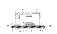
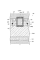
- FIG. 5 is a schematic cross-sectional structure diagram of a power module according to a modification of the first embodiment, taken along line III-III in FIG.
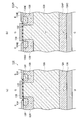
- FIG. 11 is a schematic sectional view taken along the line VII-VII in FIG. 10.
- FIG. 11 is a schematic sectional view taken along line VIII-VIII in FIG. 10. The typical cross-section figure explaining 1 process of the manufacturing method of the power module which concerns on 2nd Embodiment.
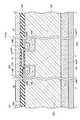
- FIG. 11 is a schematic cross-sectional structure diagram illustrating a power module according to a modification of the second embodiment, taken along line VII-VII in FIG. 10.
- FIG. 11 is a schematic cross-sectional structure diagram of a power module according to a modification of the second embodiment, taken along line VIII-VIII in FIG. 10.
- FIG. 9 is a schematic planar pattern configuration diagram showing a power module according to a third embodiment before forming a resin layer in a two-in-one module (2-in-1 module) (half-bridge built-in module).
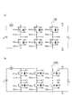
- FIG. 4 is a detailed circuit representation of the SiC MISFET of the one-in-one module, which is a power module according to the embodiment. It is a power module which concerns on embodiment, Comprising: (a) Typical circuit expression figure of SiC MISFET of a 2 in 1 module, (b) Typical circuit expression figure of IGBT of a 2 in 1 module. It is an example of the semiconductor device applied to the power module which concerns on embodiment, Comprising: (a) Typical cross-section figure of SiC MISFET, (b) Typical cross-section figure of IGBT. It is an example of the semiconductor device applied to the power module which concerns on embodiment, Comprising: The typical cross-section figure of SiC MISFET containing the source pad electrode SP and the gate pad electrode GP.
- FIG. 4 is a schematic cross-sectional structure diagram of an IGBT including an emitter pad electrode EP and a gate pad electrode GP, which is an example of a semiconductor device applied to the power module according to the embodiment.
- FIG. 1 is a schematic cross-sectional structure diagram of a SiC DI (Double-Implanted) MISFET as an example of a semiconductor device applicable to a power module according to an embodiment. It is an example of the semiconductor device applicable to the power module which concerns on embodiment, Comprising: The typical cross-section figure of SiC trench (T: Trench) MISFET.
- T Trench
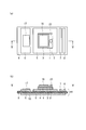
- FIG. 1A A schematic planar pattern configuration of the main part of the power module 100A according to Comparative Example 1 is represented as shown in FIG. 1A, and a schematic cross-sectional structure taken along line II in FIG. It is expressed as shown in FIG.
- a power module 100A includes a ceramic substrate 9, and a source electrode pattern 6, a drain electrode pattern 5, and a source arranged on the ceramic substrate 9. Between the signal electrode pattern 7 and the gate signal electrode pattern 8 and the drain electrode pattern 5, the semiconductor device 1 having the source pad electrode 3 and the gate pad electrode 2 on the surface side, and between the source electrode pattern 6 and the source pad electrode 3 A source bonding wire 11 connected to the source electrode, a source signal bonding wire 12 connected between the source electrode pattern 6 and the source signal electrode pattern 7, and a gate signal bonding connected between the gate pad electrode 2 and the gate signal electrode pattern 8. Wire 13 is provided. In FIG. 1 (b), the source signal bonding wire 12 is not shown in order to show the cross-sectional structure taken along the line II in FIG. 1 (a). 13 together with FIG.
- the semiconductor device 1 is bonded to the drain electrode pattern (copper foil) 5 through the under-chip solder layer 4.
- the drain electrode pattern 5 is bonded to the ceramic substrate 9 together with the metal foil of the source electrode pattern 6, the source signal electrode pattern 7, the gate signal electrode pattern 8, and the back electrode pattern 9, and is integrated as an insulating substrate 14.
- a source pad electrode 3 and a gate pad electrode 2 are formed on the surface of the semiconductor device 1, and the source pad electrode 3 and the source electrode pattern 6 are electrically connected by a source bonding wire 11.
- the gate pad electrode 2 and the gate signal electrode pattern 8 are electrically connected by a gate signal bonding wire 13. Further, the source pad electrode 3 and the source signal electrode pattern 7 are electrically connected by a source signal bonding wire 12.
- the aluminum wire melts, so it is necessary to increase the number of aluminum wires or increase the diameter ⁇ of the aluminum wires.
- the area of the source pad electrode 3 on the surface of the semiconductor chip 1 is limited, it is difficult to increase the number of aluminum wires and increase the diameter ⁇ of the aluminum wires.
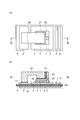
- Comparative Example 2 A schematic planar pattern configuration of the main part of the power module 100A according to Comparative Example 2 is represented as shown in FIG. 2A, and a schematic cross-sectional structure taken along line II-II in FIG. It is expressed as shown in FIG. Further, in the power module 100A according to the modified example of the comparative example 2, a schematic cross-sectional structure taken along line II-II in FIG. 2A is expressed as shown in FIG.
- a power module 100A includes a ceramic substrate 9, and a source electrode pattern 6, a drain electrode pattern 5, and a source arranged on the ceramic substrate 9. Between the signal electrode pattern 7 and the gate signal electrode pattern 8 and the drain electrode pattern 5, the semiconductor device 1 having the source pad electrode 3 and the gate pad electrode 2 on the surface side, and between the source electrode pattern 6 and the source pad electrode 3 A lead frame 15 connected to the gate electrode, a source signal bonding wire 12 connected between the source electrode pattern 6 and the source signal electrode pattern 7, and a gate signal bonding wire connected between the gate pad electrode 2 and the gate signal electrode pattern 8. 13.
- FIG. 1 In FIG.
- the source signal bonding wire 12 is not shown in order to show the cross-sectional structure taken along the line II-II in FIG. 2 (a), but in order to make the connection relationship easier to see, the gate signal bonding wire is not shown. 13 together with FIG.
- the lead frame 15 is connected to the source pad electrode 3 on the surface of the semiconductor device 1 through the on-chip solder layer 16 instead of the aluminum wire. ing.
- the lead frame 15 is connected to the source electrode pattern 6 via the source electrode pattern upper solder layer 17.
- the difference in coefficient of thermal expansion between the lead frame 15 and the semiconductor device 1 is large, a large stress load (stress) is applied to the on-chip solder layer 16 in a repetitive cooling and heating environment, and the on-chip solder layer 16 is cracked. May occur.
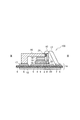
- a structure in which the stress relaxation layer 18 is interposed between the lead frame 15 and the semiconductor device 1 may be employed.
- the lead frame 15 is connected to the stress relaxation layer 18 via the stress relaxation layer upper solder layer 19.
- the current conduction area can be increased as compared with the wiring using the aluminum wire, so that a larger amount of current can flow than the aluminum wire.
- the semiconductor device 1 is soldered on the insulating substrate 14, the source signal bonding wire 12 and the gate signal bonding wire 13 are connected, and then the lead frame 15 is soldered. It is necessary to attach.
- an aluminum wire bonding bonding tool (for example, a capillary) interferes with the lead frame 15. Therefore, the source signal bonding wire 12 and the gate signal bonding wire 13 need to be bonded before the lead frame 15 is connected.
- the method for manufacturing the power module 100A according to the comparative example 2 includes the step of soldering the semiconductor device 1 on the insulating substrate 14, the step of connecting the source signal bonding wire 12 and the gate signal bonding wire 13, and the lead frame 15. Soldering.
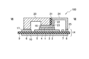
- FIG. 4A A schematic planar pattern configuration of the main part of the power module 100 according to the first embodiment is represented as shown in FIG. 4A, and is a schematic cross section taken along line III-III in FIG. 4A. The structure is represented as shown in FIG.
- the power module 100 includes a semiconductor device 1 and lead frames (20, 22) bonded to the upper surface of the semiconductor device 1.
- the lead frame (20, 22) is divided into a plurality of pieces.
- the lead frame (20, 22) divided into a plurality includes a first lead frame 20 through which a main current is conducted and a second lead frame 22 that is electrically insulated from the first lead frame 20.
- the power module 100 includes an insulating portion 21, and the first lead frame 20 and the second lead frame 22 include an insulating portion.
- Assemble connection via 21 In FIG. 4B, the source signal bonding wire 12 is not shown in order to show a cross-sectional structure taken along the line III-III in FIG. 4A, but the gate signal bonding wire 13 is shown in order to make the connection relationship easier to see. It is shown together.
- the power module 100 includes a ceramic substrate 9 and a source electrode pattern disposed on the ceramic substrate 9. 6, drain electrode pattern 5, source signal electrode pattern 7 and gate signal electrode pattern 8, semiconductor device 1 disposed on drain electrode pattern 5 and having source pad electrode 3 and gate pad electrode 2 on the surface side, and source electrode A source split lead frame 20 joined to the pattern 6 and the source pad electrode 3 and a gate pad electrode split lead frame 22 joined to the gate pad electrode 2 are provided.
- the power module 100 includes source signal bonding for connecting between the source divided lead frame 20 and the source signal electrode pattern 7.
- a wire 12 and a gate signal bonding wire 13 for connecting the gate pad electrode divided lead frame 22 and the gate signal electrode pattern 8 are provided.
- the source divided lead frame 20 and the gate pad electrode divided lead frame 22 have an insulating portion (separated). Part) 21 is assembled and connected in advance.
- the divided lead frame structure (20/22) is joined to the source pad electrode 3 and the gate pad electrode 2 on the upper surface of the semiconductor device 1 by soldering.
- the source divided lead frame 20 and the gate pad electrode divided lead frame 22 are insulated and connected to each other by an insulating portion (divided portion) 21.
- the main current from the semiconductor device 1 can be conducted to the source divided lead frame 20.
- the gate signal (voltage) from the gate pad electrode 2 is applied to the divided lead frame for gate pad electrode 22 insulated from the divided lead frame for source 20 via the insulating portion (divided portion) 21.
- the material of the insulating part (divided part) 21 may be an insulating material that can withstand a solder melting temperature that melts at about 180 ° C., for example.
- a solder melting temperature that melts at about 180 ° C.
- an epoxy resin or a silicone resin can be applied.
- the withstand voltage applied between the source divided lead frame 20 and the gate pad electrode divided lead frame 22 is, for example, about 20V. Therefore, in consideration of surge resistance, the insulating part (divided part) 21 only needs to be able to hold a withstand voltage of about 3 times about 60V.
- Cu, Al, Cu alloy, Al alloy, or an alloy including one or more of these can be used as the material of the divided lead frame 20 for source capable of conducting the main current.
- Cu, Al, CuMo, etc. can be applied as the material of the divided lead frame 22 for gate pad electrodes to which the signal voltage is applied.
- FIG. 1 A schematic planar pattern configuration for explaining one process of the method for manufacturing the power module 100 according to the first embodiment is expressed as shown in FIG. Also, a schematic cross-sectional structure taken along line IV-IV in FIG. 5A is represented as shown in FIG.
- FIG. 6A a schematic planar pattern configuration for explaining one step of the method for manufacturing the power module according to the first embodiment is expressed as shown in FIG. Further, a schematic cross-sectional structure taken along line VV in FIG. 6A is represented as shown in FIG.
- FIG. 7 part 3
- FIG. 8A a schematic planar pattern configuration for explaining one step of the method for manufacturing the power module according to the first embodiment is expressed as shown in FIG.
- FIG. 8A a schematic cross-sectional structure taken along line VI-VI in FIG. 8A is represented as shown in FIG.
- an insulating substrate 14 is prepared, and the surface-side copper foil of the ceramic substrate 9 is patterned. As a result of this patterning step, as shown in FIGS. 5A and 5B, a drain electrode pattern 5, a source electrode pattern 6, a source signal electrode pattern 7, and a gate signal electrode pattern are formed on the ceramic substrate 9. 8 is formed.
- the insulating substrate 14 for example, a DBC (Direct Bonding Copper) substrate, a DBA (Direct Brazed Aluminum) substrate, an AMB (Active Metal Brazed, Active Metal Bond) substrate, or the like is applicable. Note that an organic insulating resin layer may be used as the insulating layer substrate instead of the DBC substrate.
- the semiconductor device 1 is formed on the insulating substrate 14 by a soldering process. That is, the back electrode (drain electrode) of the semiconductor device 1 is electrically connected to the drain electrode pattern 5 via the under-chip solder layer 4.
- the source pad electrode 3 and the gate pad electrode 2 are disposed on the surface side of the semiconductor device 1, so that the source pad electrode 3.
- the on-chip solder layer 16 and the gate pad electrode solder layer 23 are formed on the gate pad electrode 2.
- a solder layer 17 on the source electrode pattern 6 is formed on the source electrode pattern 6.
- the divided lead frame 20 for source and the divided lead frame 22 for gate pad electrode are connected through an insulating portion (divided portion) 21 by an assembling process.
- the structure (20, 21, 22) is formed.
- the divided lead frame structure (20, 21, 22) is aligned on the insulating substrate 14 on which the semiconductor device 1 is mounted on the surface side.
- the source divided lead frame 20, the source electrode pattern 6, and the source pad electrode 3 are soldered between the source lead pattern 20 and the source pad pattern 3 by a soldering process. Electrical connection is made via the layer 17 and the solder layer 16 on the chip.
- the gate pad electrode divided lead frame 22 and the gate pad electrode 2 are electrically connected via the solder layer 23 on the gate pad electrode.
- the gate pad electrode divided lead frame 22 and the gate signal electrode pattern 8 are connected using the gate signal bonding wire 13.
- the source divided lead frame 20 and the source signal electrode pattern 7 are connected using the source signal bonding wire 12.
- the source electrode pattern solder layer 17 and the chip solder layer 16 may be formed in advance on the source divided lead frame 20 side.
- the solder layer 23 on the gate pad electrode may be formed on the divided lead frame 22 side for the gate pad electrode.
- an on-chip solder layer 16 and a gate pad electrode solder layer 23 are formed on the source pad electrode 3 and the gate pad electrode 2, and a source electrode pattern solder layer 17 is formed on the source electrode pattern 6.
- the step of performing can be omitted.
- the step of electrically connecting the semiconductor device 1 and the divided lead frame structure (20, 21, 22) on the insulating substrate 14 by a soldering step may be performed simultaneously.
- FIGS. 5A and 5B an insulating substrate 14 is prepared, and the surface-side copper foil of the ceramic substrate 9 is patterned.
- B1 Next, as shown in the upper drawing of FIG. 7, the source divided lead frame 20 and the gate pad electrode divided lead frame 22 are connected via an insulating portion (divided portion) 21 by an assembly process. A split lead frame structure (20, 21, 22) is formed.
- C1 Next, as shown in FIG. 8A and FIG. 8B, the semiconductor device 1 is electrically connected to the drain electrode pattern 5 via the under-chip solder layer 4 by a soldering process. To do.
- the source divided lead frame 20 and the source electrode pattern 6 and the source pad electrode 3 are electrically connected via the source electrode pattern solder layer 17 and the chip upper solder layer 16.
- the gate pad electrode divided lead frame 22 and the gate pad electrode 2 are electrically connected via the solder layer 23 on the gate pad electrode.
- D1 Next, as shown in FIG. 4A and FIG. 4B, the gate pad electrode divided lead frame 22 and the gate signal electrode pattern 8 are connected using the gate signal bonding wire 13. Further, the source divided lead frame 20 and the source signal electrode pattern 7 are connected using the source signal bonding wire 12.
- the semiconductor device 1 and the divided lead frame structure (20, 21, 22) may be simultaneously bonded to the insulating substrate 14 by a soldering process. Thus, soldering may be performed once. Further, after the semiconductor device 1 is soldered to the insulating substrate 14, the divided lead frame structure (20, 21, 22) may be soldered to the insulating substrate 14. Thus, soldering may be performed in two steps.
- the source signal bonding wire 12 and the gate signal bonding wire 13 are electrically connected to the source signal electrode pattern 7 and the gate signal electrode pattern 8 using an aluminum wire, respectively.
- the process sequence of soldering ⁇ wire bonding ⁇ soldering is soldering ⁇ wire bonding, or according to the method of manufacturing the power module 100 according to the first embodiment.
- the process sequence is soldering ⁇ soldering ⁇ wire bonding, and the number of processes can be reduced or the efficiency can be improved.
- FIG. 9 shows a schematic cross-sectional structure of the power module 100 according to the modification of the first embodiment, taken along the line III-III in FIG.
- the power module 100 is disposed on the chip solder layer 16 disposed on the source pad electrode 3 and the chip solder layer 16.
- a stress relaxation layer 18 that relieves stress applied to the upper solder layer 16 and a stress relaxation layer upper solder layer 19 disposed on the stress relaxation layer 18 are provided, and the source divided lead frame 20 is interposed via the stress relaxation layer 18. And connected to the source pad electrode 3.
- the stress generated in the on-chip solder layer 16 due to the difference in thermal expansion coefficient between the source divided lead frame 20 and the semiconductor device 1 can be relaxed.
- a metal having a low thermal expansion coefficient such as CuMo, CuW, Mo, or W can be used.
- Cu, Al, Kovar, Invar, etc. can be applied.
- the divided lead frame structure (20, 21, 22) can be connected to both the source pad electrode 3 and the gate pad electrode 2. It is.
- the method for manufacturing the power module 100 according to the first embodiment includes a step of soldering the semiconductor device 1 on the insulating substrate 14 and soldering the lead frames 20 and 22 to the semiconductor device 1, and a source signal bonding wire 12. And a step of connecting the gate signal bonding wire 13. That is, in the method for manufacturing the power module 100 according to the first embodiment, the semiconductor device 1 and the lead frames 20 and 22 can be soldered to the insulating substrate 14 at a time, and the manufacturing process can be simplified. Yes, manufacturing costs can be reduced.
- a power module that has a simple structure, that is simplified in manufacturing process, and that can conduct a large current, and a manufacturing method thereof.
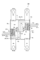
- FIG. 11 A schematic planar pattern configuration of the main part is represented as shown in FIG. Further, a schematic cross-sectional structure taken along line VII-VII in FIG. 10 is represented as shown in FIG. 11, and a schematic cross-sectional structure taken along line VIII-VIII in FIG. 10 is represented as shown in FIG. .
- the power module 100 is electrically connected to the source divided lead frame 20 and is arranged on the source signal electrode pattern 7.
- a split lead frame 26 and a gate split lead frame 24 electrically connected to the gate pad electrode split lead frame 22 and disposed on the gate signal electrode pattern 8 are provided.
- the gate divided lead frame 24 is joined to the gate signal electrode pattern 8 through the gate divided lead frame lower solder layer 25.
- the source signal divided lead frame 26 is joined to the source signal electrode pattern 7 via the source signal divided lead frame lower solder layer 27.
- the source signal split lead frame 26 may be made of the same material as the source split lead frame 20.
- the gate divided lead frame 24 may be made of the same material as the gate pad electrode divided lead frame 22.
- the gate lead electrode split lead frame 22 is extended, and the gate split lead frame 24 also serving as a gate signal line is provided. Integrated connection.
- the source split lead frame 20 is extended to serve as the source sense signal line.
- the frame 26 is integrally connected.
- the source signal bonding wire and the gate signal bonding wire are not required. Can do.
- FIGS. 1 A schematic cross-sectional structure for explaining one step of the method for manufacturing the power module according to the second embodiment is expressed as shown in FIGS.
- an insulating substrate 14 is prepared, and the surface-side copper foil of the ceramic substrate 9 is patterned. As a result of this patterning step, as shown in FIGS. 5A and 5B, a drain electrode pattern 5, a source electrode pattern 6, a source signal electrode pattern 7, and a gate signal electrode pattern are formed on the ceramic substrate 9. 8 is formed.
- the insulating substrate 14 for example, a DBC substrate, a DBA substrate, an AMB substrate, or the like is applicable. Note that an organic insulating resin layer may be used as the insulating layer substrate instead of the DBC substrate.
- the semiconductor device 1 is formed on the insulating substrate 14 by a soldering process. That is, the back electrode (drain electrode) of the semiconductor device 1 is electrically connected to the drain electrode pattern 5 via the under-chip solder layer 4.
- the source pad electrode 3 and the gate pad electrode 2 are arranged on the front surface side of the semiconductor device 1, the on-chip solder layer 16. A solder layer 23 on the gate pad electrode is formed. Similarly, a solder layer 17 on the source electrode pattern 6 is formed on the source electrode pattern 6.
- D Next, as shown in the upper drawings of FIG. 13 and FIG. 14, the source divided lead frame 20 and the gate pad electrode divided lead frame 22 are connected through the insulating portion (divided portion) 21 by an assembly process.
- the source divided lead frame 20 and the source signal divided lead frame 26 are integrally connected, the gate pad electrode divided lead frame 22 and the gate divided lead frame 24 are integrally connected, and a divided lead frame structure ( 20 ⁇ 21 ⁇ 22 ⁇ 24 ⁇ 26).
- the divided lead frame structure (20, 21, 22, 24, 26) is aligned on the insulating substrate 14 on which the semiconductor device 1 is mounted on the surface side.
- the solder layer 17 on the source electrode pattern and the solder on the chip Electrical connection is made through layer 16.
- the gate pad electrode divided lead frame 22 and the gate pad electrode 2 are electrically connected via the solder layer 23 on the gate pad electrode.
- the gate divided lead frame 24 and the gate signal electrode pattern 8 are electrically connected via the gate divided lead frame lower solder layer 25, and the source signal divided lead frame 26 and the source signal electrode pattern 7 are sourced. Electrical connection is made through the signal divided lead frame lower solder layer 27.
- the source electrode pattern solder layer 17 and the chip solder layer 16 may be formed in advance on the source divided lead frame 20 side.
- the solder layer 23 on the gate pad electrode may be formed in advance on the gate pad electrode divided lead frame 22 side.
- the gate divided lead frame lower solder layer 25 may be formed in advance on the gate divided lead frame 24 side.
- the source signal divided lead frame lower solder layer 27 may be formed in advance on the source signal divided lead frame 26 side.
- an on-chip solder layer 16 and a gate pad electrode solder layer 23 are formed on the source pad electrode 3 and the gate pad electrode 2, and a source electrode pattern solder layer 17 is formed on the source electrode pattern 6.
- the step of forming the source signal divided lead frame lower solder layer 27 and the gate divided lead frame lower solder layer 25 on the source signal electrode pattern 7 and the gate signal electrode pattern 8 can be omitted.
- the step of joining the semiconductor device 1 and the divided lead frame structure (20, 21, 22, 24, 26) on the insulating substrate 14 by a soldering step may be performed simultaneously.
- FIGS. 5A and 5B an insulating substrate 14 is prepared, and the surface-side copper foil of the ceramic substrate 9 is patterned.
- B1 Next, as shown in the upper drawings of FIGS. 13 and 14, the source divided lead frame 20, the gate pad electrode divided lead frame 22 and the gate divided lead frame 24 are separated from each other by an assembly process.
- the divided lead frame for source 20 and the divided lead frame for source signal 26 are integrally connected, and the divided lead frame for gate pad electrode 22 and the divided lead frame for gate 24 are integrated.
- the divided lead frame structure (20, 21, 22, 24, 26) is formed.
- C1 Next, as shown in FIGS. 13 and 14 and FIGS.
- the semiconductor device 1 is connected to the drain electrode pattern 5 via the under-chip solder layer 4 by a soldering process.
- the source divided lead frame 20 is connected to the source electrode pattern 6 and the source pad electrode 3 via the source electrode pattern solder layer 17 and the chip solder layer 16.
- the gate pad electrode divided lead frame 22 and the gate pad electrode 2 are connected via the solder layer 23 on the gate pad electrode.
- the divided lead frame for gate 24 and the gate signal electrode pattern 8 are connected via the gate divided lead frame lower solder layer 25, and the divided lead frame for source signal 26 and the source signal electrode pattern 7 are divided for source signal.
- the lead frame lower solder layer 27 is used for connection.
- the semiconductor device 1 and the divided lead frame structure (20, 21, 22, 24, 26) may be simultaneously bonded to the insulating substrate 14 by a soldering process. Thus, soldering may be performed once. Further, after the semiconductor device 1 is soldered to the insulating substrate 14, the divided lead frame structure (20, 21, 22, 24, 26) may be soldered to the insulating substrate 14. Thus, soldering may be performed in two steps.
- the order of steps of soldering ⁇ wire bonding ⁇ soldering in Comparative Example 2 is a single soldering process called simultaneous soldering.
- the number of processes can be reduced or the efficiency can be improved by performing the soldering process or the soldering process of soldering ⁇ soldering twice.
- the productivity can be greatly improved, and the manufacturing cost can be reduced.
- the power module 100 is disposed on the chip solder layer 16 disposed on the source pad electrode 3 and on the chip solder layer 16.
- a stress relaxation layer 18 for relaxing stress applied to the on-chip solder layer 16 and a stress relaxation layer upper solder layer 19 disposed on the stress relaxation layer 18, and the source divided lead frame 20 includes a stress relaxation layer. 18 is connected to the source pad electrode 3.
- the stress generated in the on-chip solder layer 16 due to the difference in thermal expansion coefficient between the source divided lead frame 20 and the semiconductor device 1 can be relaxed.
- a metal having a low thermal expansion coefficient such as CuMo, CuW, Mo, or W can be used.
- Cu, Al, Kovar, Invar, etc. can be applied.
- the second embodiment and its modification it is possible to provide a power module that has a simple structure, that is simplified in manufacturing process, and that can conduct a large current, and a manufacturing method thereof.
- the power module 200 has a configuration of a half-bridge built-in module in which two MISFETs Q1 and Q4 are built in one module.
- FIG. 17 shows an example in which MISFETs Q1 and Q4 are arranged in parallel in four chips.
- the power module 200 includes a positive power terminal P and a negative power terminal N arranged on the first side of the ceramic substrate 9 covered with the resin layer 115.
- the gate terminal GT1 and the source sense terminal SST1 are connected to the gate signal electrode pattern GL1 and the source signal electrode pattern SL1 of the MISFET Q1, and the gate terminal GT4 and the source sense terminal SST4 are connected to the gate of the MISFET Q4.
- the signal electrode pattern GL4 is connected to the source signal electrode pattern SL4.
- the gate divided lead frame 24 1 .multidot.1 is directed from the MISFETs Q1 and Q4 toward the gate signal electrode patterns GL1 and GL4 and the source sense signal electrode patterns SL1 and SL4 arranged on the signal substrates 124 1 and 124 4.
- 24 4 and source signal lead frames 26 1 and 26 4 are connected.
- gate terminals GT1 and GT4 for external extraction and SST1 and SST4 are connected to the gate signal electrode patterns GL1 and GL4 and the source signal electrode patterns SL1 and SL4 by soldering or the like.
- the signal substrates 124 1 and 124 4 are connected to the ceramic substrate 9 by soldering or the like.
- diodes may be connected in antiparallel between D1 and S1 and between D4 and S4 of MISFETs Q1 and Q4.
- the sources S1 and S4 of the MISFETs Q1 and Q4 arranged in parallel in four chips are connected in common by the divided lead frames 20 1 (S1) and 20 4 (S4) for source. ing.
- the positive power terminal P, the negative power terminal N, the gate terminals GT1 and GT4 for external extraction, and the SST1 and SST4 can be formed of Cu, for example.
- the signal substrates 124 1 and 124 4 can be formed of a ceramic substrate.
- the ceramic substrate may be formed of, for example, Al 2 O 3 , AlN, SiN, AlSiC, or at least the surface of insulating SiC.
- the main wiring conductors (electrode patterns) 32 1 , 32 4, and 32 n can be formed of Cu, Al, or the like, for example.
- the source divided lead frames 20 1 (S1) ⁇ 20 4 (S4) connected to the sources S1 and S4 of the MISFETs Q1 and Q4 may be made of Cu, CuMo, or the like, for example.
- the generated stress is larger in a material having a larger Young's modulus value.
- a member with a small value of generated stress can be achieved by selecting a material having a smaller value of Young's modulus ⁇ CTE.
- CuMo has such advantages.
- CuMo is inferior to Cu, its electrical resistivity is relatively low.
- the separation distance along the surface between the source divided lead frames 20 1 (S1) and 20 4 (S4) is called a creepage distance.
- the value of the creepage distance is, for example, about 2 mm.
- the divided lead frames for gates 24 1 and 24 4 and the divided lead frames for source signals 26 1 and 26 4 can be formed of, for example, Al, AlCu, or the like.
- SiC power devices such as SiC DIMISFET and SiC TMISFET, or GaN power devices such as GaN high electron mobility transistors (HEMT: High Electron Mobility Transistor) can be applied.
- HEMT High Electron Mobility Transistor
- power devices such as Si-based MISFETs and IGBTs are also applicable.
- the MISFET Q1 having a four-chip configuration is disposed on the main wiring conductor (electrode pattern) 32 1 via the under-chip solder layer 4.
- 4 MISFETQ4 chip configuration is disposed over the main conductor (electrode pattern) 32 4 chips under the solder layer 4 on.
- the main part of the power module 200 includes a ceramic substrate 9, a source electrode pattern 32 n disposed on the ceramic substrate 9, and a drain electrode pattern.
- 32 1 , 32 4 the source signal electrode patterns SL 1, SL 4 and the gate signal electrode patterns GL 1 , GL 4, and the drain electrode patterns 32 1 , 32 4 , and the source pad electrodes (3) and gate pad electrodes ( and semiconductor devices Q1 ⁇ Q4 with 2), a source electrode pattern 32 n ⁇ drain electrode patterns 32 4 and the source pad electrode (3) for the source divided bonded to the lead frame 20 1 (S1) ⁇ 20 4 and (S4)
- the split lead frame (22 1 ⁇ 22 4 ) for the gate pad electrode joined to the gate pad electrode (2) Prepare.
- the gate pad electrode split lead frames (22 1 , 22 4 ) are disposed below the gate split lead frames 24 1 , 24 4 , and therefore are not shown in FIG. 17.
- the drain electrode pattern 32 4 both a drain electrode of the semiconductor device Q4, since the source electrode of the semiconductor devices Q1, is connected to the source for dividing the lead frame 20 1 (S1).
- the power module 200 is electrically connected to the source divided lead frames 20 1 (S1) and 20 4 (S4), and has a source signal electrode pattern.
- the source signal divided lead frames 26 1 , 26 4 and the gate pad electrode divided lead frames (22 1 , 22 4 ) disposed on SL 1, SL 4 are electrically connected to the gate signal electrode patterns GL 1, GL 4.
- the gate divided lead frames 24 1 and 24 4 are provided.
- the gate divided lead frames 24 1 and 24 4 are insulated from the source divided lead frames 20 1 (S1) and 20 4 (S4). Assemble connected via (21).
- the insulating part (separating part) (21) is not shown.
- the gate divided lead frames 24 1 and 24 4 are joined to the gate signal electrode patterns GL1 and GL4 via the gate divided lead frame lower solder layer (25).
- the source signal divided lead frames 26 1 and 26 4 are joined to the source signal electrode patterns SL1 and SL4 via the source signal divided lead frame lower solder layer (27).
- the source signal split lead frames 26 1 and 26 4 may be made of the same material as the source split lead frames 20 1 (S1) and 20 4 (S4).
- the divided lead frames 24 1 and 24 4 for gates may be made of the same material as the divided lead frames for gate pads (22 1 and 22 4 ).
- the split lead frame for gate pads (22 1 , 22 4 ) is extended to split the gate lead that also serves as the gate signal line.
- the frames 24 1 and 24 4 are integrally connected.
- the source divided lead frames 20 1 (S1) and 20 4 (S4) are extended so that the source sense signal line is
- the source signal split lead frames 26 1 and 26 4 are also integrally connected.
- a source signal bonding wire is used.
- -A gate signal bonding wire can be dispensed with.
- the stress relaxation layer 18 is divided into the source divided lead frame 20 1 (S1). -You may arrange
- a two-in-one module (half-bridge built-in module) can be provided as a power module having a simple structure, a simplified manufacturing process, and capable of conducting a large current.
- the schematic circuit representation of the SiC MISFET of the one-in-one module which is the power module 220 according to the embodiment, is represented as illustrated in FIG. 20A, and the schematic circuit representation of the IGBT of the one-in-one module is illustrated in FIG. It is expressed as shown in 20 (b).
- FIG. 20A shows a diode DI connected in antiparallel to the MISFETQ.
- the main electrode of the MISFET Q is represented by a drain terminal DT and a source terminal ST.
- FIG. 20B shows a diode DI connected in reverse parallel to the IGBTQ.
- the main electrode of the IGBTQ is represented by a collector terminal CT and an emitter terminal ET.
- the power module 220 has, for example, a one-in-one module configuration. That is, one MISFETQ is built in one module. As an example, five chips (MISFET ⁇ 5) can be mounted, and up to five MISFETs Q can be connected in parallel. A part of the five chips can be mounted for the diode DI.
- a sense MISFET Qs is connected in parallel to the MISFET Q.
- the sense MISFET Qs is formed as a fine transistor in the same chip as the MISFET Q.
- SS is a source sense terminal
- CS is a current sense terminal
- G is a gate signal terminal.
- the sense MISFET Qs is formed as a fine transistor in the same chip.
- FIG. 1 a schematic circuit representation of the SiC MISFET of the power module 200T according to the embodiment and a two-in-one module is expressed as shown in FIG.
- G1 is a gate signal terminal of the MISFET Q1
- S1 is a source terminal of the MISFET Q1.
- G4 is a gate signal terminal of the MISFET Q4, and S4 is a source terminal of the MISFET Q4.
- P is a positive power input terminal
- N is a negative power input terminal
- O is an output terminal.
- FIG. 22B a schematic circuit representation of the IGBT of the power module 200T according to the embodiment and a two-in-one module is expressed as shown in FIG.
- FIG. 22B two IGBTs Q1 and Q4 and diodes D1 and D4 connected in reverse parallel to the IGBTs Q1 and Q4 are built in one module.
- G1 is a gate signal terminal of the IGBT Q1
- E1 is an emitter terminal of the IGBT Q1.
- G4 is a gate signal terminal of the IGBT Q4, and E4 is an emitter terminal of the IGBT Q4.
- P is a positive power input terminal
- N is a negative power input terminal
- O is an output terminal.
- a schematic cross-sectional structure of the SiC MISFET is a semiconductor substrate 126 made of an n ⁇ high resistance layer as shown in FIG.
- An n + drain region 124 and a drain electrode 136 connected to the n + drain region 124 are provided.
- the semiconductor device 110 is composed of a planar gate type n-channel vertical SiC MISFET. However, as shown in FIG. 27 described later, the semiconductor device 110 may be composed of an n-channel vertical SiC TMISFET or the like. good.
- GaN-based FET or the like can be employed instead of the SiC MISFET as the semiconductor device 110 (Q) applicable to the power module according to the embodiment.
- SiC-based or GaN-based power devices can be employed.
- a semiconductor having a band gap energy of, for example, 1.1 eV to 8 eV can be used.
- the IGBT includes a semiconductor substrate 126 made of an n ⁇ high resistance layer and a semiconductor as shown in FIG.
- a p body region 128 formed on the surface side of the substrate 126, an emitter region 130E formed on the surface of the p body region 128, and a gate insulating film 132 disposed on the surface of the semiconductor substrate 126 between the p body regions 128.
- a gate electrode 138 disposed on the gate insulating film 132, an emitter electrode 134E connected to the emitter region 130E and the p body region 128, and a p + collector disposed on the back surface opposite to the surface of the semiconductor substrate 126.
- a region 124P and a collector electrode 136C connected to the p + collector region 124P are provided.
- the semiconductor device 110A is composed of a planar gate type n-channel vertical IGBT, but may be composed of a trench gate type n-channel vertical IGBT or the like.
- FIG. 24 shows a schematic cross-sectional structure of an SiC MISFET that is an example of the semiconductor device 110 applicable to the power module according to the embodiment and includes the source pad electrode SP and the gate pad electrode GP.
- Gate pad electrode GP is connected to gate electrode 138 arranged on gate insulating film 132, and source pad electrode SP is connected to source electrode 134 connected to source region 130 and p body region 128.
- the gate pad electrode GP and the source pad electrode SP are disposed on a passivation interlayer insulating film 144 that covers the surface of the semiconductor device 110. Note that a fine transistor structure may be formed in the semiconductor substrate 126 below the gate pad electrode GP and the source pad electrode SP, as in the central portion of FIG.
- the source pad electrode SP may be extended and disposed on the passivation interlayer insulating film 144.
- Gate pad electrode GP is connected to gate electrode 138 disposed on gate insulating film 132, and emitter pad electrode EP is connected to emitter region 134E and emitter electrode 134E connected to p body region 128.
- the gate pad electrode GP and the emitter pad electrode EP are disposed on the passivation interlayer 144 for covering the surface of the semiconductor device 110A.
- a fine IGBT structure may be formed in the semiconductor substrate 126 below the gate pad electrode GP and the emitter pad electrode EP, as in the central portion of FIG. 23B or FIG.
- the emitter pad electrode EP may be arranged to extend on the interlayer insulating film 144 for passivation.
- SiC DISMISFET- It is an example of the semiconductor device 110 applicable to the power module which concerns on embodiment, Comprising: The typical cross-section of SiC DISMISFET is represented as shown in FIG.
- the SiC DISMISFET applicable to the power module according to the embodiment includes a semiconductor substrate 126 made of an n ⁇ high resistance layer, a p body region 128 formed on the surface side of the semiconductor substrate 126, n + source region 130 formed on the surface of p body region 128, gate insulating film 132 disposed on the surface of semiconductor substrate 126 between p body regions 128, and gate electrode disposed on gate insulating film 132 138, source electrode 134 connected to source region 130 and p body region 128, n + drain region 124 disposed on the back surface opposite to the front surface of semiconductor substrate 126, and n + drain region 124.
- a drain electrode 136 is a drain electrode 136.
- a p body region 128 and an n + source region 130 formed on the surface of the p body region 128 are formed by double ion implantation (DI). 130 and source electrode 134 connected to p body region 128.
- the gate pad electrode GP (not shown) is connected to the gate electrode 138 disposed on the gate insulating film 132. Further, as shown in FIG. 26, the source pad electrode SP and the gate pad electrode GP (not shown) are disposed on a passivation interlayer insulating film 144 that covers the surface of the semiconductor device 110.
- the SiC DIMISFET has a depletion layer as shown by a broken line formed in a semiconductor substrate 126 made of an n ⁇ high resistance layer sandwiched between p body regions 128.
- a channel resistance R JFET due to the JFET) effect is formed.
- a body diode BD is formed between the p body region 128 and the semiconductor substrate 126 as shown in FIG.
- SiC TMISFET It is an example of the semiconductor device 110 applicable to the power module which concerns on embodiment, Comprising: The typical cross-section of SiC TMISFET is represented as shown in FIG.
- the SiC TMISFET applicable to the power module according to the embodiment includes an n-layer semiconductor substrate 126N, a p body region 128 formed on the surface side of the semiconductor substrate 126N, and a p body region.
- a trench gate electrode 138TG formed through the gate insulating film 132 and the interlayer insulating films 144U and 144B is formed in the trench formed through the p body region 128 and extending to the semiconductor substrate 126N.
- the source pad electrode SP is connected to the source electrode 134 connected to the source region 130 and the p body region 28.
- the gate pad electrode GP (not shown) is connected to the gate electrode 138 disposed on the gate insulating film 132. Further, as shown in FIG. 27, the source pad electrode SP and the gate pad electrode GP (not shown) are disposed on a passivation interlayer insulating film 144U that covers the surface of the semiconductor device 110.
- the channel resistance R JFET associated with the junction FET (JFET) effect like the SiC DIMISFET is not formed.
- a body diode BD is formed between the p body region 128 and the semiconductor substrate 126N, as in FIG.
- a large surge voltage Ldi / dt is generated due to the high switching speed of the SiC MISFET and IGBT due to the inductance L of the connection line.
- di / dt 3 ⁇ 10 9 (A / s).
- the value of the surge voltage Ldi / dt varies depending on the value of the inductance L, the surge voltage Ldi / dt is superimposed on the power supply V.
- the surge voltage Ldi / dt can be absorbed by the snubber capacitor C connected between the power supply terminal PL and the ground terminal NL.
- the three-phase AC inverter 140 includes a gate drive unit 150, a power module unit 152 connected to the gate drive unit 150, and a three-phase AC motor unit 154.
- the power module unit 152 is connected to U-phase, V-phase, and W-phase inverters corresponding to the U-phase, V-phase, and W-phase of the three-phase AC motor unit 154.
- the gate drive unit 150 is connected to the SiC MISFETs Q1 and Q4, the SiC MISFETs Q2 and Q5, and the SiC MISFETs Q3 and Q6.
- the power module unit 152 is connected between the plus terminal (+) and minus terminal ( ⁇ ) of the converter 148 to which the storage battery (E) 146 is connected, and the SiC MISFETs Q1 and Q4, Q2 and Q5, and Q3 and Q6 of the inverter configuration are connected. Is provided. Free wheel diodes D1 to D6 are connected in antiparallel between the sources and drains of the SiC MISFETs Q1 to Q6, respectively.
- the three-phase AC inverter 140A includes a gate drive unit 150A, a power module unit 152A connected to the gate drive unit 150A, and a three-phase AC motor unit 154A.
- the power module unit 152A is connected to U-phase, V-phase, and W-phase inverters corresponding to the U-phase, V-phase, and W-phase of the three-phase AC motor unit 154A.
- the gate drive unit 150A is connected to the IGBTs Q1 and Q4, the IGBTs Q2 and Q5, and the IGBTs Q3 and Q6.
- the power module 152A is connected between the plus terminal (+) and minus terminal ( ⁇ ) of the converter 148A to which the storage battery (E) 146A is connected, and the IGBTs Q1 ⁇ Q4, Q2 ⁇ Q5, and Q3 ⁇ Q6 of the inverter configuration are connected. Prepare. Further, free wheel diodes D1 to D6 are connected in antiparallel between the emitters and collectors of IGBTs Q1 to Q6, respectively.
- the power module according to the present embodiment can be formed in one-in-one, two-in-one, four-in-one, six-in-one, or seven-in-one types.
- the present embodiment it is possible to provide a power module capable of conducting a large current with a simple structure, a simplified manufacturing process, and a method for manufacturing the power module.
- the present embodiment includes various embodiments that are not described here.
- the power module of the present embodiment can be used for semiconductor module manufacturing technology such as IGBT module, diode module, MOS module (Si, SiC, GaN), etc., inverter for HEV / EV, inverter for industrial, converter It can be applied to a wide range of application fields.
- semiconductor module manufacturing technology such as IGBT module, diode module, MOS module (Si, SiC, GaN), etc.
- inverter for HEV / EV inverter for industrial, converter It can be applied to a wide range of application fields.
Landscapes
- Inverter Devices (AREA)
- Physics & Mathematics (AREA)
- Geometry (AREA)
- Lead Frames For Integrated Circuits (AREA)
- Electrodes Of Semiconductors (AREA)
- Wire Bonding (AREA)
Abstract
パワーモジュール(100)は、セラミックス基板(9)と、セラミックス基板上に配置されたソース電極パターン(6)、ドレイン電極パターン(5)、ソース信号電極パターン(7)およびゲート信号電極パターン(8)と、ドレイン電極パターン上に配置され、表面側にソースパッド電極(3)およびゲートパッド電極(2)を有する半導体デバイス(1)と、ソース電極パターンおよびソースパッド電極に接合されたソース用分割リードフレーム(20)と、ゲートパッド電極と接合されたゲートパッド電極用分割リードフレーム(22)とを備える。構造が簡単で、製造プロセスが簡略化され、大電流化可能なパワーモジュールおよびその製造方法を提供する。
Description
本実施の形態は、パワーモジュールおよびその製造方法に関する。
従来、絶縁ゲートバイポーラトランジスタ(IGBT:Insulated Gate Bipolar Transistor)のような半導体デバイスを含むパワーチップがリードフレーム上に搭載され、系全体が樹脂でモールドされたパワーモジュールが知られている。動作状態において、半導体デバイスは発熱するため、リードフレームの裏面に絶縁層を介してヒートシンクを配置し、半導体デバイスを冷却するのが一般的である。
現在多くの研究機関において、シリコンカーバイド(SiC:Silicon Carbide)デバイスの研究開発が行われている。SiCパワーデバイスは、Siパワーデバイスよりも優れた低オン抵抗、高速スイッチングおよび高温動作特性を有する。
SiCパワーモジュールでは、SiCデバイスのロスが相対的に小さいため、大電流を導通可能であり、かつ高温動作が容易となったが、それを許容するためのパワーモジュールの設計は必須である。
SiCパワーデバイスのパッケージには、ケース型が採用されている。また、トランスファーモールドによって樹脂封止された半導体装置についても開示されている。
主電極上に柱電極構造を備えるSiCパワーデバイスにおいて、線熱膨張を調整し、薄型で作ったSiCパワーモジュールの反り量を低減化したパワーモジュールや熱抵抗を改善したSiCパワーモジュールも提案されている。
本実施の形態は、構造が簡単で、製造プロセスが簡略化され、大電流を導通可能なパワーモジュールおよびその製造方法を提供することにある。
本実施の形態の一態様によれば、半導体デバイスと、前記半導体デバイスの上面に接合されたリードフレームとを備えるパワーモジュールが提供される。
本実施の形態の他の態様によれば、基板と、前記基板上に配置された第1電極パターン、第2電極パターン、第1信号電極パターンおよび第2信号電極パターンと、前記第2電極パターン上に配置され、表面側に第1パッド電極および第2パッド電極を有する半導体デバイスと、前記第1電極パターンおよび前記第1パッド電極に接合された第1リードフレームと、前記第2パッド電極と接合された第2リードフレームとを備えるパワーモジュールが提供される。
本実施の形態の他の態様によれば、基板上に第1電極パターン、第2電極パターン、第1信号電極パターンおよび第2信号電極パターンを形成する工程と、前記第2電極パターン上に、表面側に第1パッド電極および第2パッド電極を有する半導体デバイスを形成する工程と、第1リードフレームと第2リードフレームと絶縁部とをアセンブルする工程と、前記第1電極パターンおよび前記第1パッド電極に第1リードフレームを接合し、前記第2パッド電極と第2リードフレームを接合する工程とを有するパワーモジュールの製造方法が提供される。
本実施の形態の他の態様によれば、基板上に第1電極パターン、第2電極パターン、第1信号電極パターンおよび第2信号電極パターンを形成する工程と、第1リードフレームと第2リードフレームと絶縁部とをアセンブルする工程と、前記第2電極パターン上に、表面側に第1パッド電極および第2パッド電極を有する半導体デバイスを形成すると共に、前記第1電極パターンおよび前記第1パッド電極に前記第1リードフレームを接合し、前記第2パッド電極と前記第2リードフレームを接合する工程とを有するパワーモジュールの製造方法が提供される。
本実施の形態の他の態様によれば、基板上に第1電極パターン、第2電極パターン、第1信号電極パターンおよび第2信号電極パターンを形成する工程と、前記第2電極パターン上に、表面側に第1パッド電極および第2パッド電極を有する半導体デバイスを形成する工程と、第1リードフレームと第2リードフレームとを絶縁部を介して接続し、前記第1リードフレームと第3リードフレームとを一体化接続し、前記第2リードフレームと第4リードフレームとを一体化接続し、分割リードフレーム構造をアセンブルする工程と、前記第1電極パターンおよび前記第1パッド電極に前記第1リードフレームを接合し、前記第2パッド電極と第2リードフレームを接合し、前記第1信号電極パターンと前記第3リードフレームを接合し、前記第2信号電極パターンと前記第4リードフレームを接合する工程とを有するパワーモジュールの製造方法が提供される。
本実施の形態の他の態様によれば、基板上に第1電極パターン、第2電極パターン、第1信号電極パターンおよび第2信号電極パターンを形成する工程と、第1リードフレームと第2リードフレームとを絶縁部を介して接続し、前記第1リードフレームと第3リードフレームとを一体化接続し、前記第2リードフレームと第4リードフレームとを一体化接続し、分割リードフレーム構造をアセンブルする工程と、前記第2電極パターン上に、表面側に第1パッド電極および第2パッド電極を有する半導体デバイスを形成すると共に、前記第1電極パターンおよび前記第1パッド電極に前記第1リードフレームを接合し、前記第2パッド電極と第2リードフレームを接合し、前記第1信号電極パターンと前記第3リードフレームを接合し、前記第2信号電極パターンと前記第4リードフレームを接合する工程とを有するパワーモジュールの製造方法が提供される。
本実施の形態によれば、構造が簡単で、製造プロセスが簡略化され、大電流を導通可能なパワーモジュールおよびその製造方法を提供することができる。
次に、図面を参照して、本実施の形態を説明する。以下の図面の記載において、同一又は類似の部分には同一又は類似の符号を付している。ただし、図面は模式的なものであり、各構成部品の厚みと平面寸法との関係等は現実のものとは異なることに留意すべきである。したがって、具体的な厚みや寸法は以下の説明を参酌して判断すべきものである。又、図面相互間においても互いの寸法の関係や比率が異なる部分が含まれていることはもちろんである。
又、以下に示す実施の形態は、技術的思想を具体化するための装置や方法を例示するものであって、各構成部品の材質、形状、構造、配置等を下記のものに特定するものでない。実施の形態は、特許請求の範囲において、種々の変更を加えることができる。
[比較例]
―比較例1―
比較例1に係るパワーモジュール100Aの主要部の模式的平面パターン構成は、図1(a)に示すように表わされ、図1(a)のI-I線に沿う模式的断面構造は、図1(b)に示すように表わされる。
―比較例1―
比較例1に係るパワーモジュール100Aの主要部の模式的平面パターン構成は、図1(a)に示すように表わされ、図1(a)のI-I線に沿う模式的断面構造は、図1(b)に示すように表わされる。
比較例1に係るパワーモジュール100Aは、図1(a)および図1(b)に示すように、セラミックス基板9と、セラミックス基板9上に配置されたソース電極パターン6・ドレイン電極パターン5・ソース信号電極パターン7・ゲート信号電極パターン8と、ドレイン電極パターン5上に配置され、表面側にソースパッド電極3およびゲートパッド電極2を有する半導体デバイス1と、ソース電極パターン6・ソースパッド電極3間に接続されたソースボンディングワイヤ11と、ソース電極パターン6・ソース信号電極パターン7間に接続されたソース信号ボンディングワイヤ12と、ゲートパッド電極2・ゲート信号電極パターン8間に接続されたゲート信号ボンディングワイヤ13とを備える。尚、図1(b)においては、図1(a)のI-I線に沿う断面構造を示すため、ソース信号ボンディングワイヤ12は図示されないが、接続関係を見易くするために、ゲート信号ボンディングワイヤ13と共に図示している。
半導体デバイス1は、チップ下半田層4を介してドレイン電極パターン(銅箔)5に接合される。ドレイン電極パターン5は、ソース電極パターン6・ソース信号電極パターン7・ゲート信号電極パターン8・裏面電極パターン9の金属箔と共に、セラミックス基板9に接合され、絶縁基板14として一体化されている。
半導体デバイス1の表面には、ソースパッド電極3およびゲートパッド電極2が形成されており、ソースパッド電極3とソース電極パターン6は、ソースボンディングワイヤ11によって、電気的に接続されている。また、ゲートパッド電極2とゲート信号電極パターン8は、ゲート信号ボンディングワイヤ13によって、電気的に接続されている。さらに、ソースパッド電極3とソース信号電極パターン7は、ソース信号ボンディングワイヤ12によって、電気的に接続されている。
ソースボンディングワイヤ11には、通常直径φ=400μm程度のアルミワイヤが用いられるが、導通可能な最大電流は、ワイヤ1本当たり25A程度である。例えば、4mm角の半導体チップ表面のソースパッド電極3に接合可能なワイヤ本数は、直径φ=400μm程度のアルミワイヤであれば、最大4本程度である。したがって、この4mm角の半導体チップに導通可能な最大電流は、25A×4=100A程度となる。これ以上導通させると、アルミワイヤの溶断が起こるため、アルミワイヤの本数を増加するか、アルミワイヤの直径φを太くする必要がある。しかしながら、半導体チップ1表面のソースパッド電極3の面積が限られているため、アルミワイヤの本数を増加することもアルミワイヤの直径φを太くすることも難しい。
―比較例2―
比較例2に係るパワーモジュール100Aの主要部の模式的平面パターン構成は、図2(a)に示すように表わされ、図2(a)のII-II線に沿う模式的断面構造は、図2(b)に示すように表わされる。また、比較例2の変形例に係るパワーモジュール100Aであって、図2(a)のII-II線に沿う模式的断面構造は、図3に示すように表わされる。
比較例2に係るパワーモジュール100Aの主要部の模式的平面パターン構成は、図2(a)に示すように表わされ、図2(a)のII-II線に沿う模式的断面構造は、図2(b)に示すように表わされる。また、比較例2の変形例に係るパワーモジュール100Aであって、図2(a)のII-II線に沿う模式的断面構造は、図3に示すように表わされる。
比較例2に係るパワーモジュール100Aは、図2(a)および図2(b)に示すように、セラミックス基板9と、セラミックス基板9上に配置されたソース電極パターン6・ドレイン電極パターン5・ソース信号電極パターン7・ゲート信号電極パターン8と、ドレイン電極パターン5上に配置され、表面側にソースパッド電極3およびゲートパッド電極2を有する半導体デバイス1と、ソース電極パターン6・ソースパッド電極3間に接続されたリードフレーム15と、ソース電極パターン6・ソース信号電極パターン7間に接続されたソース信号ボンディングワイヤ12と、ゲートパッド電極2・ゲート信号電極パターン8間に接続されたゲート信号ボンディングワイヤ13とを備える。尚、図2(b)においては、図2(a)のII-II線に沿う断面構造を示すため、ソース信号ボンディングワイヤ12は図示されないが、接続関係を見易くするために、ゲート信号ボンディングワイヤ13と共に図示している。
図2(a)および図2(b)に示すように、リードフレーム配線では、アルミワイヤの代わりにリードフレーム15がチップ上半田層16を介して半導体デバイス1表面のソースパッド電極3に接続されている。また、リードフレーム15は、ソース電極パターン上半田層17を介して、ソース電極パターン6に接続されている。リードフレーム15の材料としては、導電率が高い銅や銅合金などを適用可能である。
また、リードフレーム15と半導体デバイス1との熱膨張率差が大きいため、冷熱繰り返し環境下において、チップ上半田層16に大きな応力負荷(ストレス)が加わり、チップ上半田層16にクラックが生じる不具合が起きることがある。このため、比較例2の変形例においては、図3に示すように、リードフレーム15と半導体デバイス1間に応力緩和層18を介在させる構造を採用することもある。ここで、リードフレーム15は、応力緩和層上半田層19を介して、応力緩和層18に接続される。
これらのリードフレーム構造では、アルミワイヤを用いた配線に比べ、電流の導通面積を増やすことができるため、アルミワイヤよりも多くの電流を流すことが可能となる。一方、ゲートパッド電極2・ゲート信号電極パターン8間には、ゲート信号ボンディングワイヤ13を接続し、ソースパッド電極3・ソース信号電極パターン7間には、ソース信号ボンディングワイヤ12を接続する必要があるため、製造工程上効率が悪い。例えば、図2に示す比較例2の構造においては、絶縁基板14上に半導体デバイス1を半田付けした後、ソース信号ボンディングワイヤ12・ゲート信号ボンディングワイヤ13を接続し、その後、リードフレーム15を半田付けする必要がある。ソース信号ボンディングワイヤ12・ゲート信号ボンディングワイヤ13の接続前に、リードフレーム15を半田付けしてしまうと、アルミワイヤボンディングのボンディングツール(例えば、キャピラリーなど)が、リードフレーム15に干渉してしまう。このため、ソース信号ボンディングワイヤ12・ゲート信号ボンディングワイヤ13は、リードフレーム15の接続前に、ボンディングを実施しておく必要がある。
したがって、比較例2に係るパワーモジュール100Aの製造方法は、絶縁基板14上に半導体デバイス1を半田付けする工程と、ソース信号ボンディングワイヤ12・ゲート信号ボンディングワイヤ13を接続する工程と、リードフレーム15を半田付けする工程とを有する。
[第1の実施の形態]
(パワーモジュール)
第1の実施の形態に係るパワーモジュール100の主要部の模式的平面パターン構成は、図4(a)に示すように表わされ、図4(a)のIII-III線に沿う模式的断面構造は、図4(b)に示すように表わされる。
(パワーモジュール)
第1の実施の形態に係るパワーモジュール100の主要部の模式的平面パターン構成は、図4(a)に示すように表わされ、図4(a)のIII-III線に沿う模式的断面構造は、図4(b)に示すように表わされる。
第1の実施の形態に係るパワーモジュール100は、図4(a)および図4(b)に示すように、半導体デバイス1と、半導体デバイス1の上面に接合されたリードフレーム(20、22)とを備える。ここで、リードフレーム(20、22)は、複数に分割されている。
複数に分割されたリードフレーム(20、22)は、主電流が導通する第1リードフレーム20と、第1リードフレーム20と電気的に絶縁された第2リードフレーム22とを備える。
第1の実施の形態に係るパワーモジュール100は、図4(a)および図4(b)に示すように、絶縁部21を備え、第1リードフレーム20と第2リードフレーム22は、絶縁部21を介してアセンブル接続される。尚、図4(b)において、図4(a)のIII-III線に沿う断面構造を示すため、ソース信号ボンディングワイヤ12は図示されないが、接続関係を見易くするために、ゲート信号ボンディングワイヤ13と共に図示している。
さらに詳細には、第1の実施の形態に係るパワーモジュール100は、図4(a)および図4(b)に示すように、セラミックス基板9と、セラミックス基板9上に配置されたソース電極パターン6、ドレイン電極パターン5、ソース信号電極パターン7およびゲート信号電極パターン8と、ドレイン電極パターン5上に配置され、表面側にソースパッド電極3およびゲートパッド電極2を有する半導体デバイス1と、ソース電極パターン6およびソースパッド電極3に接合されたソース用分割リードフレーム20と、ゲートパッド電極2と接合されたゲートパッド電極用分割リードフレーム22とを備える。
第1の実施の形態に係るパワーモジュール100は、図4(a)および図4(b)に示すように、ソース用分割リードフレーム20とソース信号電極パターン7との間を接続するソース信号ボンディングワイヤ12と、ゲートパッド電極用分割リードフレーム22とゲート信号電極パターン8との間を接続するゲート信号ボンディングワイヤ13とを備える。
第1の実施の形態に係るパワーモジュール100は、図4(a)および図4(b)に示すように、ソース用分割リードフレーム20とゲートパッド電極用分割リードフレーム22は、絶縁部(分離部)21を介して予めアセンブル接続される。
第1の実施の形態に係るパワーモジュール100において、半導体デバイス1の上面のソースパッド電極3とゲートパッド電極2に対して、分割リードフレーム構造(20・22)が半田付けにより接合される。ここで、ソース用分割リードフレーム20とゲートパッド電極用分割リードフレーム22は、絶縁部(分割部)21によって互いに絶縁されかつ接続されている。ソース用分割リードフレーム20には、半導体デバイス1からの主電流が導通可能である。一方、ソース用分割リードフレーム20と絶縁部(分割部)21を介して絶縁されたゲートパッド電極用分割リードフレーム22には、ゲートパッド電極2からのゲート信号(電圧)が印加される。
絶縁部(分割部)21の材料としては、例えば、約180℃で溶融する半田溶融温度に耐える絶縁材料であれば良い。例えば、エポキシ系樹脂、シリコーン系樹脂を適用可能である。また、ソース用分割リードフレーム20とゲートパッド電極用分割リードフレーム22間に印加される絶縁耐圧としては、例えば、約20Vである。したがって、サージ耐量を考慮して、絶縁部(分割部)21は約3倍の60V程度の耐圧が保持可能であれば良い。
主電流が導通可能なソース用分割リードフレーム20の材料としては、Cu、Al、Cu合金、Al合金またはこれらを1つ以上含む合金などを適用可能である。
信号電圧が印加されるゲートパッド電極用分割リードフレーム22の材料としては、Cu、Al、CuMoなどを適用可能である。
(製造方法)
第1の実施の形態に係るパワーモジュール100の製造方法の一工程を説明する模式的平面パターン構成は、図5(a)に示すように表わされる(その1)。また、図5(a)のIV-IV線に沿う模式的断面構造は、図5(b)に示すように表わされる。
第1の実施の形態に係るパワーモジュール100の製造方法の一工程を説明する模式的平面パターン構成は、図5(a)に示すように表わされる(その1)。また、図5(a)のIV-IV線に沿う模式的断面構造は、図5(b)に示すように表わされる。
また、第1の実施の形態に係るパワーモジュールの製造方法の一工程を説明する模式的平面パターン構成は、図6(a)に示すように表わされる(その2)。また、図6(a)のV-V線に沿う模式的断面構造は、図6(b)に示すように表わされる。
さらに、第1の実施の形態に係るパワーモジュールの製造方法の一工程を説明する模式的断面構造は、図7に示すように表される(その3)。
さらに、第1の実施の形態に係るパワーモジュールの製造方法の一工程を説明する模式的平面パターン構成は、図8(a)に示すように表わされる(その4)。また、図8(a)のVI-VI線に沿う模式的断面構造は、図8(b)に示すように表わされる。
(a)まず、図5(a)および図5(b)に示すように、絶縁基板14を準備し、セラミックス基板9の表面側銅箔をパターニングする。このパターニング工程の結果として、図5(a)および図5(b)に示すように、セラミックス基板9上には、ドレイン電極パターン5・ソース電極パターン6・ソース信号電極パターン7・ゲート信号電極パターン8が形成される。ここで、絶縁基板14としては、例えば、DBC(Direct Bonding Copper)基板、DBA(Direct Brazed Aluminum)基板若しくはAMB(Active Metal Brazed, Active Metal Bond)基板などを適用可能である。なお、DBC基板の代わりに、有機絶縁樹脂層を絶縁層基板として適用しても良い。
(b)次に、図6(a)および図6(b)に示すように、絶縁基板14上に半導体デバイス1を半田付け工程によって形成する。すなわち、ドレイン電極パターン5上にチップ下半田層4を介して、半導体デバイス1の裏面電極(ドレイン電極)を電気的に接続する。
(c)次に、図6(a)および図6(b)に示すように、半導体デバイス1の表面側には、ソースパッド電極3・ゲートパッド電極2が配置されているため、ソースパッド電極3・ゲートパッド電極2に対して、チップ上半田層16・ゲートパッド電極上半田層23を形成する。同様に、ソース電極パターン6上にソース電極パターン上半田層17を形成する。
(d)次に、図7に示すように、アセンブル工程によって、ソース用分割リードフレーム20とゲートパッド電極用分割リードフレーム22とを絶縁部(分割部)21を介して接続し、分割リードフレーム構造(20・21・22)を形成する。
(e)さらに、図7に示すように、分割リードフレーム構造(20・21・22)を、半導体デバイス1を表面側に搭載した絶縁基板14上にアライメントする。
(f)次に、図8(a)および図8(b)に示すように、半田付け工程によって、ソース用分割リードフレーム20とソース電極パターン6およびソースパッド電極3間をソース電極パターン上半田層17・チップ上半田層16を介して電気的に接続する。同時に、ゲートパッド電極用分割リードフレーム22とゲートパッド電極2間をゲートパッド電極上半田層23を介して電気的に接続する。
(g)次に、図4(a)および図4(b)に示すように、ゲートパッド電極用分割リードフレーム22とゲート信号電極パターン8間をゲート信号ボンディングワイヤ13を用いて接続する。また、ソース用分割リードフレーム20とソース信号電極パターン7間をソース信号ボンディングワイヤ12を用いて接続する。
(b)次に、図6(a)および図6(b)に示すように、絶縁基板14上に半導体デバイス1を半田付け工程によって形成する。すなわち、ドレイン電極パターン5上にチップ下半田層4を介して、半導体デバイス1の裏面電極(ドレイン電極)を電気的に接続する。
(c)次に、図6(a)および図6(b)に示すように、半導体デバイス1の表面側には、ソースパッド電極3・ゲートパッド電極2が配置されているため、ソースパッド電極3・ゲートパッド電極2に対して、チップ上半田層16・ゲートパッド電極上半田層23を形成する。同様に、ソース電極パターン6上にソース電極パターン上半田層17を形成する。
(d)次に、図7に示すように、アセンブル工程によって、ソース用分割リードフレーム20とゲートパッド電極用分割リードフレーム22とを絶縁部(分割部)21を介して接続し、分割リードフレーム構造(20・21・22)を形成する。
(e)さらに、図7に示すように、分割リードフレーム構造(20・21・22)を、半導体デバイス1を表面側に搭載した絶縁基板14上にアライメントする。
(f)次に、図8(a)および図8(b)に示すように、半田付け工程によって、ソース用分割リードフレーム20とソース電極パターン6およびソースパッド電極3間をソース電極パターン上半田層17・チップ上半田層16を介して電気的に接続する。同時に、ゲートパッド電極用分割リードフレーム22とゲートパッド電極2間をゲートパッド電極上半田層23を介して電気的に接続する。
(g)次に、図4(a)および図4(b)に示すように、ゲートパッド電極用分割リードフレーム22とゲート信号電極パターン8間をゲート信号ボンディングワイヤ13を用いて接続する。また、ソース用分割リードフレーム20とソース信号電極パターン7間をソース信号ボンディングワイヤ12を用いて接続する。
(製造工程の短縮化・効率化)
以上の製造工程においては、ソース電極パターン上半田層17・チップ上半田層16は予め、ソース用分割リードフレーム20側に形成しても良い。同様に、ゲートパッド電極上半田層23は、ゲートパッド電極用分割リードフレーム22側に形成しても良い。この場合には、ソースパッド電極3・ゲートパッド電極2に対して、チップ上半田層16・ゲートパッド電極上半田層23を形成し、ソース電極パターン6上にソース電極パターン上半田層17を形成する工程は省略可能である。
以上の製造工程においては、ソース電極パターン上半田層17・チップ上半田層16は予め、ソース用分割リードフレーム20側に形成しても良い。同様に、ゲートパッド電極上半田層23は、ゲートパッド電極用分割リードフレーム22側に形成しても良い。この場合には、ソースパッド電極3・ゲートパッド電極2に対して、チップ上半田層16・ゲートパッド電極上半田層23を形成し、ソース電極パターン6上にソース電極パターン上半田層17を形成する工程は省略可能である。
また、絶縁基板14上に半導体デバイス1および分割リードフレーム構造(20・21・22)を半田付け工程により電気的に接続する工程を同時に実施しても良い。
(a1)まず、図5(a)および図5(b)に示すように、絶縁基板14を準備し、セラミックス基板9の表面側銅箔をパターニングする。
(b1)次に、図7の上部図面に示すように、アセンブル工程によって、ソース用分割リードフレーム20とゲートパッド電極用分割リードフレーム22とを絶縁部(分割部)21を介して接続し、分割リードフレーム構造(20・21・22)を形成する。
(c1)次に、図8(a)および図8(b)に示すように、半田付け工程によって、ドレイン電極パターン5上にチップ下半田層4を介して、半導体デバイス1を電気的に接続する。同時に、ソース用分割リードフレーム20とソース電極パターン6およびソースパッド電極3間をソース電極パターン上半田層17・チップ上半田層16を介して電気的に接続する。同時に、ゲートパッド電極用分割リードフレーム22とゲートパッド電極2間をゲートパッド電極上半田層23を介して電気的に接続する。
(d1)次に、図4(a)および図4(b)に示すように、ゲートパッド電極用分割リードフレーム22とゲート信号電極パターン8間をゲート信号ボンディングワイヤ13を用いて接続する。また、ソース用分割リードフレーム20とソース信号電極パターン7間をソース信号ボンディングワイヤ12を用いて接続する。
(b1)次に、図7の上部図面に示すように、アセンブル工程によって、ソース用分割リードフレーム20とゲートパッド電極用分割リードフレーム22とを絶縁部(分割部)21を介して接続し、分割リードフレーム構造(20・21・22)を形成する。
(c1)次に、図8(a)および図8(b)に示すように、半田付け工程によって、ドレイン電極パターン5上にチップ下半田層4を介して、半導体デバイス1を電気的に接続する。同時に、ソース用分割リードフレーム20とソース電極パターン6およびソースパッド電極3間をソース電極パターン上半田層17・チップ上半田層16を介して電気的に接続する。同時に、ゲートパッド電極用分割リードフレーム22とゲートパッド電極2間をゲートパッド電極上半田層23を介して電気的に接続する。
(d1)次に、図4(a)および図4(b)に示すように、ゲートパッド電極用分割リードフレーム22とゲート信号電極パターン8間をゲート信号ボンディングワイヤ13を用いて接続する。また、ソース用分割リードフレーム20とソース信号電極パターン7間をソース信号ボンディングワイヤ12を用いて接続する。
半導体デバイス1と分割リードフレーム構造(20・21・22)は、半田付け工程によって、絶縁基板14に対して同時に接合しても良い。このように、一回で半田付けしても良い。また、半導体デバイス1を絶縁基板14に対して半田付け接続した後に、分割リードフレーム構造(20・21・22)を絶縁基板14に対して半田付け接続しても良い。このように、2回に分けて半田付けしても良い。
このような半田付け工程の後に、ソース信号ボンディングワイヤ12およびゲート信号ボンディングワイヤ13をそれぞれソース信号電極パターン7およびゲート信号電極パターン8にアルミワイヤを用いて電気的に接続する。
以上の工程により、比較例2において、半田付け⇒ワイヤボンディング⇒半田付けとしていた工程順序が、第1の実施の形態に係るパワーモジュール100の製造方法によれば、半田付け⇒ワイヤボンディング、或いは、半田付け⇒半田付け⇒ワイヤボンディングという工程順序となり、工程数の短縮或いは効率化を図ることができる。
(変形例)
第1の実施の形態の変形例に係るパワーモジュール100であって、図4(a)のIII-III線に沿う模式的断面構造は、図9に示すように表わされる。
第1の実施の形態の変形例に係るパワーモジュール100であって、図4(a)のIII-III線に沿う模式的断面構造は、図9に示すように表わされる。
第1の実施の形態の変形例に係るパワーモジュール100は、図9に示すように、ソースパッド電極3上に配置されたチップ上半田層16と、チップ上半田層16上に配置され、チップ上半田層16に加わる応力を緩和する応力緩和層18と、応力緩和層18上に配置された応力緩和層上半田層19とを備え、ソース用分割リードフレーム20は、応力緩和層18を介して、ソースパッド電極3に接続される。
第1の実施の形態の変形例に係るパワーモジュール100においては、ソース用分割リードフレーム20と半導体デバイス1との熱膨張係数差によってチップ上半田層16に生じる応力を緩和することができる。
応力緩和層18の材料としては、CuMo、CuW、Mo、Wなどの低熱膨張係数金属を用いることができる。或いは、Cu、Al、コバール、インバーなどを適用可能である。
第1の実施の形態に係るパワーモジュール100においては、リードフレームを分割構造とすることによって、分割リードフレーム構造(20・21・22)をソースパッド電極3とゲートパッド電極2の両方に接続可能である。
第1の実施の形態に係るパワーモジュール100の製造方法は、絶縁基板14上に半導体デバイス1を半田付けすると共に半導体デバイス1にリードフレーム20・22を半田付けする工程と、ソース信号ボンディングワイヤ12・ゲート信号ボンディングワイヤ13を接続する工程とを有する。すなわち、第1の実施の形態に係るパワーモジュール100の製造方法においては、 半導体デバイス1とリードフレーム20・22を絶縁基板14上に一度に半田付けすることができ、製造工程が簡略化可能であり、製造コストダウンを図ることができる。
第1の実施の形態およびその変形例によれば、構造が簡単で、製造プロセスが簡略化され、大電流を導通可能なパワーモジュールおよびその製造方法を提供することができる。
[第2の実施の形態]
の主要部の模式的平面パターン構成は、図10に示すように表わされる。また、図10のVII-VII線に沿う模式的断面構造は、図11に示すように表わされ、図10のVIII-VIII線に沿う模式的断面構造は、図12に示すように表わされる。
の主要部の模式的平面パターン構成は、図10に示すように表わされる。また、図10のVII-VII線に沿う模式的断面構造は、図11に示すように表わされ、図10のVIII-VIII線に沿う模式的断面構造は、図12に示すように表わされる。
第2の実施の形態に係るパワーモジュール100は、図10~図12に示すように、ソース用分割リードフレーム20と電気的に接続され、かつソース信号電極パターン7上に配置されたソース信号用分割リードフレーム26と、ゲートパッド電極用分割リードフレーム22と電気的に接続され、かつゲート信号電極パターン8上に配置されたゲート用分割リードフレーム24とを備える。
ゲート用分割リードフレーム24は、ゲート用分割リードフレーム下半田層25を介して、ゲート信号電極パターン8と接合される。
ソース信号用分割リードフレーム26は、ソース信号用分割リードフレーム下半田層27を介して、ソース信号電極パターン7と接合される。
なお、ソース信号用分割リードフレーム26は、ソース用分割リードフレーム20と同一材料を備えていても良い。
また、ゲート用分割リードフレーム24は、ゲートパッド電極用分割リードフレーム22と同一材料を備えていても良い。
その他の構成および構成材料は、第1の実施の形態と同様である。
第2の実施の形態に係るパワーモジュール100においては、図10および図11に示すように、ゲートパッド電極用分割リードフレーム22を延伸させて、ゲート信号線を兼ねたゲート用分割リードフレーム24と一体化接続させている。
同様に、第2の実施の形態に係るパワーモジュール100においては、図10および図12に示すように、ソース用分割リードフレーム20を延伸させて、ソースセンス信号線を兼ねたソース信号用分割リードフレーム26と一体化接続させている。
第2の実施の形態に係るパワーモジュール100においては、このような分割リードフレーム構造(20、22、26、24)を採用することによって、ソース信号ボンディングワイヤ・ゲート信号ボンディングワイヤを不要とすることができる。
(製造方法)
第2の実施の形態に係るパワーモジュールの製造方法の一工程を説明する模式的断面構造は、図13および図14に示すように表される。
第2の実施の形態に係るパワーモジュールの製造方法の一工程を説明する模式的断面構造は、図13および図14に示すように表される。
(a)まず、図5(a)および図5(b)に示すように、絶縁基板14を準備し、セラミックス基板9の表面側銅箔をパターニングする。このパターニング工程の結果として、図5(a)および図5(b)に示すように、セラミックス基板9上には、ドレイン電極パターン5・ソース電極パターン6・ソース信号電極パターン7・ゲート信号電極パターン8が形成される。ここで、絶縁基板14としては、例えば、DBC基板、DBA基板若しくはAMB基板などを適用可能である。なお、DBC基板の代わりに、有機絶縁樹脂層を絶縁層基板として適用しても良い。
(b)次に、図6(a)および図6(b)に示すように、絶縁基板14上に半導体デバイス1を半田付け工程によって形成する。すなわち、ドレイン電極パターン5上にチップ下半田層4を介して、半導体デバイス1の裏面電極(ドレイン電極)を電気的に接続する。
(c)次に、半導体デバイス1の表面側には、ソースパッド電極3・ゲートパッド電極2が配置されているため、ソースパッド電極3・ゲートパッド電極2に対して、チップ上半田層16・ゲートパッド電極上半田層23を形成する。同様に、ソース電極パターン6上にソース電極パターン上半田層17を形成する。
(d)次に、図13・図14の上部図面に示すように、アセンブル工程によって、ソース用分割リードフレーム20とゲートパッド電極用分割リードフレーム22とを絶縁部(分割部)21を介して接続し、ソース用分割リードフレーム20とソース信号用分割リードフレーム26と一体化接続し、ゲートパッド電極用分割リードフレーム22とゲート用分割リードフレーム24とを一体化接続し、分割リードフレーム構造(20・21・22・24・26)を形成する。
(e)さらに、図13・図14に示すように、分割リードフレーム構造(20・21・22・24・26)を、半導体デバイス1を表面側に搭載した絶縁基板14上にアライメントする。
(f)次に、図10~図12に示すように、半田付け工程によって、ソース用分割リードフレーム20とソース電極パターン6およびソースパッド電極3間をソース電極パターン上半田層17・チップ上半田層16を介して電気的に接続する。同時に、ゲートパッド電極用分割リードフレーム22とゲートパッド電極2間をゲートパッド電極上半田層23を介して電気的に接続する。同時に、ゲート用分割リードフレーム24とゲート信号電極パターン8間をゲート用分割リードフレーム下半田層25を介して電気的に接続し、ソース信号用分割リードフレーム26とソース信号電極パターン7間をソース信号用分割リードフレーム下半田層27を介して電気的に接続する。
(b)次に、図6(a)および図6(b)に示すように、絶縁基板14上に半導体デバイス1を半田付け工程によって形成する。すなわち、ドレイン電極パターン5上にチップ下半田層4を介して、半導体デバイス1の裏面電極(ドレイン電極)を電気的に接続する。
(c)次に、半導体デバイス1の表面側には、ソースパッド電極3・ゲートパッド電極2が配置されているため、ソースパッド電極3・ゲートパッド電極2に対して、チップ上半田層16・ゲートパッド電極上半田層23を形成する。同様に、ソース電極パターン6上にソース電極パターン上半田層17を形成する。
(d)次に、図13・図14の上部図面に示すように、アセンブル工程によって、ソース用分割リードフレーム20とゲートパッド電極用分割リードフレーム22とを絶縁部(分割部)21を介して接続し、ソース用分割リードフレーム20とソース信号用分割リードフレーム26と一体化接続し、ゲートパッド電極用分割リードフレーム22とゲート用分割リードフレーム24とを一体化接続し、分割リードフレーム構造(20・21・22・24・26)を形成する。
(e)さらに、図13・図14に示すように、分割リードフレーム構造(20・21・22・24・26)を、半導体デバイス1を表面側に搭載した絶縁基板14上にアライメントする。
(f)次に、図10~図12に示すように、半田付け工程によって、ソース用分割リードフレーム20とソース電極パターン6およびソースパッド電極3間をソース電極パターン上半田層17・チップ上半田層16を介して電気的に接続する。同時に、ゲートパッド電極用分割リードフレーム22とゲートパッド電極2間をゲートパッド電極上半田層23を介して電気的に接続する。同時に、ゲート用分割リードフレーム24とゲート信号電極パターン8間をゲート用分割リードフレーム下半田層25を介して電気的に接続し、ソース信号用分割リードフレーム26とソース信号電極パターン7間をソース信号用分割リードフレーム下半田層27を介して電気的に接続する。
(製造工程の短縮化・効率化)
以上の製造工程においては、ソース電極パターン上半田層17・チップ上半田層16は予め、ソース用分割リードフレーム20側に形成しても良い。同様に、ゲートパッド電極上半田層23は予め、ゲートパッド電極用分割リードフレーム22側に形成しても良い。同様に、ゲート用分割リードフレーム下半田層25は予め、ゲート用分割リードフレーム24側に形成しても良い。同様に、ソース信号用分割リードフレーム下半田層27は予め、ソース信号用分割リードフレーム26側に形成しても良い。この場合には、ソースパッド電極3・ゲートパッド電極2に対して、チップ上半田層16・ゲートパッド電極上半田層23を形成し、ソース電極パターン6上にソース電極パターン上半田層17を形成し、ソース信号電極パターン7・ゲート信号電極パターン8上にソース信号用分割リードフレーム下半田層27・ゲート用分割リードフレーム下半田層25を形成する工程は省略可能である。
以上の製造工程においては、ソース電極パターン上半田層17・チップ上半田層16は予め、ソース用分割リードフレーム20側に形成しても良い。同様に、ゲートパッド電極上半田層23は予め、ゲートパッド電極用分割リードフレーム22側に形成しても良い。同様に、ゲート用分割リードフレーム下半田層25は予め、ゲート用分割リードフレーム24側に形成しても良い。同様に、ソース信号用分割リードフレーム下半田層27は予め、ソース信号用分割リードフレーム26側に形成しても良い。この場合には、ソースパッド電極3・ゲートパッド電極2に対して、チップ上半田層16・ゲートパッド電極上半田層23を形成し、ソース電極パターン6上にソース電極パターン上半田層17を形成し、ソース信号電極パターン7・ゲート信号電極パターン8上にソース信号用分割リードフレーム下半田層27・ゲート用分割リードフレーム下半田層25を形成する工程は省略可能である。
また、絶縁基板14上に半導体デバイス1および分割リードフレーム構造(20・21・22・24・26)を半田付け工程により接合する工程を同時に実施しても良い。
(a1)まず、図5(a)および図5(b)に示すように、絶縁基板14を準備し、セラミックス基板9の表面側銅箔をパターニングする。
(b1)次に、図13・図14の上部図面に示すように、アセンブル工程によって、ソース用分割リードフレーム20とゲートパッド電極用分割リードフレーム22・ゲート用分割リードフレーム24とを絶縁部(分割部)21を介して接続し、かつソース用分割リードフレーム20とソース信号用分割リードフレーム26とを一体化接続し、ゲートパッド電極用分割リードフレーム22とゲート用分割リードフレーム24とを一体化接続し、分割リードフレーム構造(20・21・22・24・26)を形成する。
(c1)次に、図13・図14および図10~図12に示すように、半田付け工程によって、ドレイン電極パターン5上にチップ下半田層4を介して、半導体デバイス1を接続する。同時に、ソース用分割リードフレーム20とソース電極パターン6およびソースパッド電極3間をソース電極パターン上半田層17・チップ上半田層16を介して接続する。同時に、ゲートパッド電極用分割リードフレーム22とゲートパッド電極2間をゲートパッド電極上半田層23を介して接続する。同時に、ゲート用分割リードフレーム24とゲート信号電極パターン8間をゲート用分割リードフレーム下半田層25を介して接続し、ソース信号用分割リードフレーム26とソース信号電極パターン7間をソース信号用分割リードフレーム下半田層27を介して接続する。
(b1)次に、図13・図14の上部図面に示すように、アセンブル工程によって、ソース用分割リードフレーム20とゲートパッド電極用分割リードフレーム22・ゲート用分割リードフレーム24とを絶縁部(分割部)21を介して接続し、かつソース用分割リードフレーム20とソース信号用分割リードフレーム26とを一体化接続し、ゲートパッド電極用分割リードフレーム22とゲート用分割リードフレーム24とを一体化接続し、分割リードフレーム構造(20・21・22・24・26)を形成する。
(c1)次に、図13・図14および図10~図12に示すように、半田付け工程によって、ドレイン電極パターン5上にチップ下半田層4を介して、半導体デバイス1を接続する。同時に、ソース用分割リードフレーム20とソース電極パターン6およびソースパッド電極3間をソース電極パターン上半田層17・チップ上半田層16を介して接続する。同時に、ゲートパッド電極用分割リードフレーム22とゲートパッド電極2間をゲートパッド電極上半田層23を介して接続する。同時に、ゲート用分割リードフレーム24とゲート信号電極パターン8間をゲート用分割リードフレーム下半田層25を介して接続し、ソース信号用分割リードフレーム26とソース信号電極パターン7間をソース信号用分割リードフレーム下半田層27を介して接続する。
半導体デバイス1と分割リードフレーム構造(20・21・22・24・26)は、半田付け工程によって、絶縁基板14に対して同時に接合しても良い。このように、一回で半田付けしても良い。また、半導体デバイス1を絶縁基板14に対して半田付け接続した後に、分割リードフレーム構造(20・21・22・24・26)を絶縁基板14に対して半田付け接続しても良い。このように、2回に分けて半田付けしても良い。
以上の工程により、比較例2において、半田付け⇒ワイヤボンディング⇒半田付けとしていた工程順序が、第2の実施の形態に係るパワーモジュール100の製造方法によれば、同時半田付けという1回の半田付け工程、或いは、半田付け⇒半田付けという2回の半田付け工程となり、工程数の短縮或いは効率化を図ることができる。
第2の実施の形態に係るパワーモジュール100の製造方法においては、製造工程が簡略化されるため、生産性が大幅に向上可能であり、製造コストダウンを図ることができる。
(変形例)
第2の実施の形態の変形例に係るパワーモジュール100であって、図10のVII-VII線に沿う模式的断面構造は、図15に示すように表わされ、図10のVIII-VIII線に沿う模式的断面構造は、図16に示すように表わされる。
第2の実施の形態の変形例に係るパワーモジュール100であって、図10のVII-VII線に沿う模式的断面構造は、図15に示すように表わされ、図10のVIII-VIII線に沿う模式的断面構造は、図16に示すように表わされる。
第2の実施の形態の変形例に係るパワーモジュール100は、図15・図16に示すように、ソースパッド電極3上に配置されたチップ上半田層16と、チップ上半田層16上に配置され、チップ上半田層16に加わる応力を緩和する応力緩和層18と、応力緩和層18上に配置された応力緩和層上半田層19とを備え、ソース用分割リードフレーム20は、応力緩和層18を介して、ソースパッド電極3に接続される。
第2の実施の形態の変形例に係るパワーモジュール100においては、ソース用分割リードフレーム20と半導体デバイス1との熱膨張係数差によってチップ上半田層16に生じる応力を緩和することができる。
応力緩和層18の材料としては、CuMo、CuW、Mo、Wなどの低熱膨張係数金属を用いることができる。或いは、Cu、Al、コバール、インバーなどを適用可能である。
第2の実施の形態およびその変形例によれば、構造が簡単で、製造プロセスが簡略化され、大電流を導通可能なパワーモジュールおよびその製造方法を提供することができる。
[第3の実施の形態]
第3の実施の形態に係るパワーモジュール200であって、ツーインワンモジュール(2 in 1 Module:ハーフブリッジ内蔵モジュール)において、樹脂層115を形成前の模式的平面パターン構成は図17に示すように表され、樹脂層115を形成後の模式的鳥瞰構成は図19に示すように表される。また、第3の実施の形態に係るパワーモジュールであって、半導体デバイスとしてSiC MISFETを適用した図17に対応したツーインワンモジュール(ハーフブリッジ内蔵モジュール)の回路構成は、図18に示すように表される。
第3の実施の形態に係るパワーモジュール200であって、ツーインワンモジュール(2 in 1 Module:ハーフブリッジ内蔵モジュール)において、樹脂層115を形成前の模式的平面パターン構成は図17に示すように表され、樹脂層115を形成後の模式的鳥瞰構成は図19に示すように表される。また、第3の実施の形態に係るパワーモジュールであって、半導体デバイスとしてSiC MISFETを適用した図17に対応したツーインワンモジュール(ハーフブリッジ内蔵モジュール)の回路構成は、図18に示すように表される。
第3の実施の形態に係るパワーモジュール200は、2個のMISFETQ1・Q4が1つのモジュールに内蔵されたハーフブリッジ内蔵モジュールの構成を備える。
図17においては、MISFETQ1・Q4は、それぞれ4チップ並列に配置されている例が示されている。
第3の実施の形態に係るパワーモジュール200は、図19に示すように、樹脂層115に被覆されたセラミックス基板9の第1の辺に配置された正側電力端子Pおよび負側電力端子Nと、第1の辺に隣接する第2の辺に配置されたゲート端子GT1・ソースセンス端子SST1と、第1の辺に対向する第3の辺に配置された出力端子Oと、第2の辺に対向する第4の辺に配置されたゲート端子GT4・ソースセンス端子SST4とを備える。ここで、図17に示すように、ゲート端子GT1・ソースセンス端子SST1は、MISFETQ1のゲート信号電極パターンGL1・ソース信号電極パターンSL1に接続され、ゲート端子GT4・ソースセンス端子SST4は、MISFETQ4のゲート信号電極パターンGL4・ソース信号電極パターンSL4に接続される。
図17に示すように、MISFETQ1・Q4から信号基板1241・1244上に配置されたゲート信号電極パターンGL1・GL4およびソースセンス信号電極パターンSL1・SL4に向けてゲート用分割リードフレーム241・244およびソース信号用リードフレーム261・264が接続される。また、ゲート信号電極パターンGL1・GL4およびソース信号電極パターンSL1・SL4には、外部取り出し用のゲート端子GT1・GT4およびSST1・SST4が半田付けなどによって接続される。
図17に示すように、信号基板1241・1244は、セラミックス基板9上に、半田付けなどによって接続される。
また、図17~図19においては、図示は省略されているが、MISFETQ1・Q4のD1・S1間およびD4・S4間に逆並列にダイオードが接続されていても良い。
図17~図19に示された例では、4チップ並列に配置されたMISFETQ1・Q4のソースS1・S4は、ソース用分割リードフレーム201(S1)・204(S4)によって共通に接続されている。
正側電力端子P・負側電力端子N、外部取り出し用のゲート端子GT1・GT4およびSST1・SST4は、例えば、Cuで形成可能である。
信号基板1241・1244は、セラミックス基板で形成可能である。セラミックス基板は、例えば、Al2O3、AlN、SiN、AlSiC、若しくは少なくとも表面が絶縁性のSiCなどで形成されていても良い。
主配線導体(電極パターン)321・324・32nは、例えば、Cu、Alなどで形成可能である。
MISFETQ1・Q4のソースS1・S4と接続されるソース用分割リードフレーム201(S1)・204(S4)は、例えば、Cu、CuMoなどで形成されていても良い。CTEの値が同等である同じ大きさの材料を比較すると、発生応力は、ヤング率の値が大きい材料の方が大きくなる。このため、ヤング率×CTEの数値が、より小さい材料を選定することによって、発生応力の値の小さな部材を達成することができる。CuMoは、このような利点を有している。また、CuMoは、Cuには劣るが、電気抵抗率も相対的に低い。また、ソース用分割リードフレーム201(S1)・204(S4)間の表面に沿った離隔距離は、沿面距離と呼ばれる。沿面距離の値は、例えば、約2mmである。
ゲート用分割リードフレーム241・244およびソース信号用分割リードフレーム261・264は、例えば、Al、AlCuなどで形成可能である。
MISFETQ1・Q4としては、SiC DIMISFET、SiC TMISFETなどのSiC系パワーデバイス、あるいはGaN系高電子移動度トランジスタ(HEMT: High Electron Mobility Transistor)などのGaN系パワーデバイスを適用可能である。また、場合によっては、Si系MISFETやIGBTなどのパワーデバイスも適用可能である。
第3の実施の形態に係るパワーモジュール200においては、4チップ構成のMISFETQ1は、主配線導体(電極パターン)321上にチップ下半田層4を介して配置されている。同様に、4チップ構成のMISFETQ4は、主配線導体(電極パターン)324上にチップ下半田層4を介して配置されている。
さらに詳細には、第3の実施の形態に係るパワーモジュール200の主要部は、図17に示すように、セラミックス基板9と、セラミックス基板9上に配置されたソース電極パターン32n、ドレイン電極パターン321・324、ソース信号電極パターンSL1・SL4およびゲート信号電極パターンGL1・GL4と、ドレイン電極パターン321・324上に配置され、表面側にソースパッド電極(3)およびゲートパッド電極(2)を有する半導体デバイスQ1・Q4と、ソース電極パターン32n・ドレイン電極パターン324およびソースパッド電極(3)に接合されたソース用分割リードフレーム201(S1)・204(S4)と、ゲートパッド電極(2)と接合されたゲートパッド電極用分割リードフレーム(221・224)とを備える。ここで、ゲートパッド電極用分割リードフレーム(221・224)は、ゲート用分割リードフレーム241・244の下に配置されるため、図17では、図示は省略されている。また、ドレイン電極パターン324は、半導体デバイスQ4のドレイン電極であると同時に、半導体デバイスQ1のソース電極となるため、ソース用分割リードフレーム201(S1)と接続される。
さらに、第3の実施の形態に係るパワーモジュール200は、図17に示すように、ソース用分割リードフレーム201(S1)・204(S4)と電気的に接続され、かつソース信号電極パターンSL1・SL4上に配置されたソース信号用分割リードフレーム261・264と、ゲートパッド電極用分割リードフレーム(221・224)と電気的に接続され、かつゲート信号電極パターンGL1・GL4上に配置されたゲート用分割リードフレーム241・244とを備える。ゲート用分割リードフレーム241・244は、第2の実施の形態の図11と同様に、ソース用分割リードフレーム201(S1)・204(S4)に対して絶縁部(分離部)(21)を介してアセンブル接続されている。ここで、絶縁部(分離部)(21)は、図示を省略している。
ゲート用分割リードフレーム241・244は、ゲート用分割リードフレーム下半田層(25)を介して、ゲート信号電極パターンGL1・GL4と接合される。
ソース信号用分割リードフレーム261・264は、ソース信号用分割リードフレーム下半田層(27)を介して、ソース信号電極パターンSL1・SL4と接合される。
なお、ソース信号用分割リードフレーム261・264は、ソース用分割リードフレーム201(S1)・204(S4)と同一材料を備えていても良い。
また、ゲート用分割リードフレーム241・244は、ゲートパッド電極用分割リードフレーム(221・224)と同一材料を備えていても良い。
その他の構成および構成材料は、第2の実施の形態と同様である。
第3の実施の形態に係るパワーモジュール200においても、図17に示すように、ゲートパッド電極用分割リードフレーム(221・224)を延伸させて、ゲート信号線を兼ねたゲート用分割リードフレーム241・244と一体化接続させている。
同様に、第3の実施の形態に係るパワーモジュール200においては、図17に示すように、ソース用分割リードフレーム201(S1)・204(S4)を延伸させて、ソースセンス信号線を兼ねたソース信号用分割リードフレーム261・264と一体化接続させている。
第3の実施の形態に係るパワーモジュール200においては、このような分割リードフレーム構造(201・204、261・264、241・244)を採用することによって、ソース信号ボンディングワイヤ・ゲート信号ボンディングワイヤを不要とすることができる。
なお、第3の実施の形態に係るパワーモジュール200においても第2の実施の形態の変形例(図15・図16)と同様に、応力緩和層18をソース用分割リードフレーム201(S1)・204(S4)とソースパッド電極3間に配置しても良い。
第3の実施の形態に係るパワーモジュール200の製造方法も第2の実施の形態と同様であるため、説明は省略する。
第3の実施の形態によれば、構造が簡単で、製造プロセスが簡略化され、大電流を導通可能なパワーモジュールとして、ツーインワンモジュール(ハーフブリッジ内蔵モジュール)を提供することができる。
(パワーモジュールの具体例)
以下、実施の形態に係るパワーモジュールの具体例を説明する。もちろん、以下に説明するパワーモジュールにおいても、分割リードフレーム構造を採用している。
以下、実施の形態に係るパワーモジュールの具体例を説明する。もちろん、以下に説明するパワーモジュールにおいても、分割リードフレーム構造を採用している。
実施の形態に係るパワーモジュール220であって、ワンインワンモジュールのSiC MISFETの模式的回路表現は、図20(a)に示すように表され、ワンインワンモジュールのIGBTの模式的回路表現は、図20(b)に示すように表される。
図20(a)には、MISFETQに逆並列接続されるダイオードDIが示されている。MISFETQの主電極は、ドレイン端子DTおよびソース端子STで表される。同様に、図20(b)には、IGBTQに逆並列接続されるダイオードDIが示されている。IGBTQの主電極は、コレクタ端子CTおよびエミッタ端子ETで表される。
また、実施の形態に係るパワーモジュール220であって、ワンインワンモジュールのSiC MISFETの詳細回路表現は、図21に示すように表される。
実施の形態に係るパワーモジュール220は、例えば、ワンインワンモジュールの構成を備える。すなわち、1個のMISFETQが1つのモジュールに内蔵されている。一例として5チップ(MISFET×5)搭載可能であり、それぞれのMISFETQは、5個まで並列接続可能である。尚、5チップの内、一部をダイオードDI用として搭載することも可能である。
さらに詳細には、図21に示すように、MISFETQに並列にセンス用MISFETQsが接続される。センス用MISFETQsは、MISFETQと同一チップ内に、微細トランジスタとして形成されている。図21において、SSは、ソースセンス端子、CSは、電流センス端子であり、Gは、ゲート信号端子である。なお、実施の形態においても半導体デバイスQには、センス用MISFETQsが同一チップ内に、微細トランジスタとして形成されている。
また、実施の形態に係るパワーモジュール200Tであって、ツーインワンモジュールのSiC MISFETの模式的回路表現は、図22(a)に示すように表される。
図22(a)に示すように、2個のMISFETQ1・Q4と、MISFETQ1・Q4に逆並列接続されるダイオードD1・D4が1つのモジュールに内蔵されている。G1は、MISFETQ1のゲート信号端子であり、S1は、MISFETQ1のソース端子である。G4は、MISFETQ4のゲート信号端子であり、S4は、MISFETQ4のソース端子である。Pは、正側電源入力端子であり、Nは、負側電源入力端子であり、Oは、出力端子である。
また、実施の形態に係るパワーモジュール200Tであって、ツーインワンモジュールのIGBTの模式的回路表現は、図22(b)に示すように表される。図22(b)に示すように、2個のIGBTQ1・Q4と、IGBTQ1・Q4に逆並列接続されるダイオードD1・D4が1つのモジュールに内蔵されている。G1は、IGBTQ1のゲート信号端子であり、E1は、IGBTQ1のエミッタ端子である。G4は、IGBTQ4のゲート信号端子であり、E4は、IGBTQ4のエミッタ端子である。Pは、正側電源入力端子であり、Nは、負側電源入力端子であり、Oは、出力端子である。
(半導体デバイスの構成例)
実施の形態に係るパワーモジュールに適用可能な半導体デバイスの例であって、SiC MISFETの模式的断面構造は、図23(a)に示すように表され、IGBTの模式的断面構造は、図23(b)に示すように表される。
実施の形態に係るパワーモジュールに適用可能な半導体デバイスの例であって、SiC MISFETの模式的断面構造は、図23(a)に示すように表され、IGBTの模式的断面構造は、図23(b)に示すように表される。
実施の形態に係るパワーモジュールに適用可能な半導体デバイス110(Q)の例として、SiC MISFETの模式的断面構造は、図23(a)に示すように、n-高抵抗層からなる半導体基板126と、半導体基板126の表面側に形成されたpボディ領域128と、pボディ領域128の表面に形成されたソース領域130と、pボディ領域128間の半導体基板126の表面上に配置されたゲート絶縁膜132と、ゲート絶縁膜132上に配置されたゲート電極138と、ソース領域130およびpボディ領域128に接続されたソース電極134と、半導体基板126の表面と反対側の裏面に配置されたn+ドレイン領域124と、n+ドレイン領域124に接続されたドレイン電極136とを備える。
図23(a)では、半導体デバイス110は、プレーナゲート型nチャネル縦型SiC MISFETで構成されているが、後述する図27に示すように、nチャネル縦型SiC TMISFETなどで構成されていても良い。
また、実施の形態に係るパワーモジュールに適用可能な半導体デバイス110(Q)には、SiC MISFETの代わりに、GaN系FETなどを採用することもできる。
実施の形態に係るパワーモジュールに適用可能な半導体デバイス110には、SiC系、GaN系のいずれかのパワーデバイスを採用可能である。
更には、実施の形態に係るパワーモジュールに適用可能な半導体デバイス110には、バンドギャップエネルギーが、例えば、1.1eV~8eVの半導体を用いることができる。
同様に、実施の形態に係るパワーモジュールに適用可能な半導体デバイス110A(Q)の例として、IGBTは、図23(b)に示すように、n-高抵抗層からなる半導体基板126と、半導体基板126の表面側に形成されたpボディ領域128と、pボディ領域128の表面に形成されたエミッタ領域130Eと、pボディ領域128間の半導体基板126の表面上に配置されたゲート絶縁膜132と、ゲート絶縁膜132上に配置されたゲート電極138と、エミッタ領域130Eおよびpボディ領域128に接続されたエミッタ電極134Eと、半導体基板126の表面と反対側の裏面に配置されたp+コレクタ領域124Pと、p+コレクタ領域124Pに接続されたコレクタ電極136Cとを備える。
図23(b)では、半導体デバイス110Aは、プレーナゲート型のnチャネル縦型IGBTで構成されているが、トレンチゲート型nチャネル縦型IGBTなどで構成されていても良い。
実施の形態に係るパワーモジュールに適用可能な半導体デバイス110の例であって、ソースパッド電極SP、ゲートパッド電極GPを含むSiC MISFETの模式的断面構造は、図24に示すように表される。ゲートパッド電極GPは、ゲート絶縁膜132上に配置されたゲート電極138に接続され、ソースパッド電極SPは、ソース領域130およびpボディ領域128に接続されたソース電極134に接続される。
また、ゲートパッド電極GPおよびソースパッド電極SPは、図24に示すように、半導体デバイス110の表面を覆うパッシベーション用の層間絶縁膜144上に配置される。尚、ゲートパッド電極GPおよびソースパッド電極SPの下方の半導体基板126内には、図23(a)或いは、図24の中央部と同様に、微細構造のトランジスタ構造が形成されていても良い。
さらに、図24に示すように、中央部のトランジスタ構造においても、パッシベーション用の層間絶縁膜144上にソースパッド電極SPが延在して配置されていても良い。
実施の形態に係るパワーモジュール200・200Tに適用する半導体デバイス110Aの例であって、ソースパッド電極SP、ゲートパッド電極GPを含むIGBTの模式的断面構造は、図25に示すように表される。ゲートパッド電極GPは、ゲート絶縁膜132上に配置されたゲート電極138に接続され、エミッタパッド電極EPは、エミッタ領域130Eおよびpボディ領域128に接続されたエミッタ電極134Eに接続される。
また、ゲートパッド電極GPおよびエミッタパッド電極EPは、図25に示すように、半導体デバイス110Aの表面を覆うパッシベーション用の層間絶縁膜144上に配置される。尚、ゲートパッド電極GPおよびエミッタパッド電極EPの下方の半導体基板126内には、図23(b)或いは、図25の中央部と同様に、微細構造のIGBT構造が形成されていても良い。
さらに、図25に示すように、中央部のIGBT構造においても、パッシベーション用の層間絶縁膜144上にエミッタパッド電極EPが延在して配置されていても良い。
―SiC DIMISFET―
実施の形態に係るパワーモジュールに適用可能な半導体デバイス110の例であって、SiC DIMISFETの模式的断面構造は、図26に示すように表される。
実施の形態に係るパワーモジュールに適用可能な半導体デバイス110の例であって、SiC DIMISFETの模式的断面構造は、図26に示すように表される。
実施の形態に係るパワーモジュールに適用可能なSiC DIMISFETは、図26に示すように、n-高抵抗層からなる半導体基板126と、半導体基板126の表面側に形成されたpボディ領域128と、pボディ領域128の表面に形成されたn+ソース領域130と、pボディ領域128間の半導体基板126の表面上に配置されたゲート絶縁膜132と、ゲート絶縁膜132上に配置されたゲート電極138と、ソース領域130およびpボディ領域128に接続されたソース電極134と、半導体基板126の表面と反対側の裏面に配置されたn+ドレイン領域124と、n+ドレイン領域124に接続されたドレイン電極136とを備える。
図26では、半導体デバイス110は、pボディ領域128と、pボディ領域128の表面に形成されたn+ソース領域130が、ダブルイオン注入(DI)で形成され、ソースパッド電極SPは、ソース領域130およびpボディ領域128に接続されたソース電極134に接続される。ゲートパッド電極GP(図示省略)は、ゲート絶縁膜132上に配置されたゲート電極138に接続される。また、ソースパッド電極SPおよびゲートパッド電極GP(図示省略)は、図26に示すように、半導体デバイス110の表面を覆うパッシベーション用の層間絶縁膜144上に配置される。
SiC DIMISFETは、図26に示すように、pボディ領域128に挟まれたn-高抵抗層からなる半導体基板126内に、破線で示されるような空乏層が形成されるため、接合型FET(JFET)効果に伴うチャネル抵抗RJFETが形成される。また、pボディ領域128/半導体基板126間には、図26に示すように、ボディダイオードBDが形成される。
―SiC TMISFET―
実施の形態に係るパワーモジュールに適用可能な半導体デバイス110の例であって、SiC TMISFETの模式的断面構造は、図27に示すように表される。
実施の形態に係るパワーモジュールに適用可能な半導体デバイス110の例であって、SiC TMISFETの模式的断面構造は、図27に示すように表される。
実施の形態に係るパワーモジュールに適用可能なSiC TMISFETは、図27に示すように、n層からなる半導体基板126Nと、半導体基板126Nの表面側に形成されたpボディ領域128と、pボディ領域128の表面に形成されたn+ソース領域130と、pボディ領域128を貫通し、半導体基板126Nまで形成されたトレンチの内にゲート絶縁膜132および層間絶縁膜144U・144Bを介して形成されたトレンチゲート電極138TGと、ソース領域130およびpボディ領域128に接続されたソース電極134と、半導体基板126Nの表面と反対側の裏面に配置されたn+ドレイン領域124と、n+ドレイン領域124に接続されたドレイン電極136とを備える。
図27では、半導体デバイス110は、pボディ領域128を貫通し、半導体基板126Nまで形成されたトレンチ内にゲート絶縁膜132および層間絶縁膜144U・144Bを介して形成されたトレンチゲート電極138TGが形成され、ソースパッド電極SPは、ソース領域130およびpボディ領域28に接続されたソース電極134に接続される。ゲートパッド電極GP(図示省略)は、ゲート絶縁膜132上に配置されたゲート電極138に接続される。また、ソースパッド電極SPおよびゲートパッド電極GP(図示省略)は、図27に示すように、半導体デバイス110の表面を覆うパッシベーション用の層間絶縁膜144U上に配置される。
SiC TMISFETでは、SiC DIMISFETのような接合型FET(JFET)効果に伴うチャネル抵抗RJFETは形成されない。また、pボディ領域128/半導体基板126N間には、図2と同様に、ボディダイオードBDが形成される。
実施の形態に係るパワーモジュールを用いて構成した3相交流インバータ140の模式的回路構成において、半導体デバイスとしてSiC MISFETを適用し、電源端子PL、接地端子NL間にスナバコンデンサCを接続した回路構成例は、図28(a)に示すように表される。同様に、実施の形態に係るパワーモジュールを用いて構成した3相交流インバータ140Aの模式的回路構成において、半導体デバイスとしてIGBTを適用し、電源端子PL、接地端子NL間にスナバコンデンサCを接続した回路構成例は、図28(b)に示すように表される。
実施の形態に係るパワーモジュールを電源Eと接続する際、接続ラインの有するインダクタンスLによって、SiC MISFETやIGBTのスイッチング速度が速いため、大きなサージ電圧Ldi/dtを生ずる。例えば、電流変化di=300A、スイッチングに伴う時間変化dt=100nsecとすると、di/dt=3×109(A/s)となる。インダクタンスLの値により、サージ電圧Ldi/dtの値は変化するが、電源Vにこのサージ電圧Ldi/dtが重畳される。電源端子PLと接地端子NL間に接続されるスナバコンデンサCによって、このサージ電圧Ldi/dtを吸収することができる。
実施の形態に係るパワーモジュールを電源Eと接続する際、接続ラインの有するインダクタンスLによって、SiC MISFETやIGBTのスイッチング速度が速いため、大きなサージ電圧Ldi/dtを生ずる。例えば、電流変化di=300A、スイッチングに伴う時間変化dt=100nsecとすると、di/dt=3×109(A/s)となる。インダクタンスLの値により、サージ電圧Ldi/dtの値は変化するが、電源Vにこのサージ電圧Ldi/dtが重畳される。電源端子PLと接地端子NL間に接続されるスナバコンデンサCによって、このサージ電圧Ldi/dtを吸収することができる。
(パワーモジュールを適用した応用例)
次に、図29を参照して、半導体デバイスとしてSiC MISFETを適用した実施の形態に係るパワーモジュールを用いて構成した3相交流インバータ140について説明する。
次に、図29を参照して、半導体デバイスとしてSiC MISFETを適用した実施の形態に係るパワーモジュールを用いて構成した3相交流インバータ140について説明する。
図29に示すように、3相交流インバータ140は、ゲートドライブ部150と、ゲートドライブ部150に接続されたパワーモジュール部152と、3相交流モータ部154とを備える。パワーモジュール部152は、3相交流モータ部154のU相、V相、W相に対応して、U相、V相、W相のインバータが接続されている。ここで、ゲートドライブ部150は、SiC MISFETQ1・Q4、SiC MISFETQ2・Q5、およびSiC MISFETQ3・Q6に接続されている。
パワーモジュール部152は、蓄電池(E)146が接続されたコンバータ148のプラス端子(+)とマイナス端子(-)間に接続され、インバータ構成のSiC MISFETQ1・Q4、Q2・Q5、およびQ3・Q6を備える。また、SiC MISFETQ1~Q6のソース・ドレイン間には、フリーホイールダイオードD1~D6がそれぞれ逆並列に接続されている。
次に、図30を参照して、半導体デバイスとしてIGBTを適用した実施の形態に係るパワーモジュール200Tを用いて構成した3相交流インバータ140Aについて説明する。
図30に示すように、3相交流インバータ140Aは、ゲートドライブ部150Aと、ゲートドライブ部150Aに接続されたパワーモジュール部152Aと、3相交流モータ部154Aとを備える。パワーモジュール部152Aは、3相交流モータ部154AのU相、V相、W相に対応して、U相、V相、W相のインバータが接続されている。ここで、ゲートドライブ部150Aは、IGBTQ1・Q4、IGBTQ2・Q5、およびIGBTQ3・Q6に接続されている。
パワーモジュール部152Aは、蓄電池(E)146Aが接続されたコンバータ148Aのプラス端子(+)とマイナス端子(-)間に接続され、インバータ構成のIGBTQ1・Q4、Q2・Q5、およびQ3・Q6を備える。さらに、IGBTQ1~Q6のエミッタ・コレクタ間には、フリーホイールダイオードD1~D6がそれぞれ逆並列に接続されている。
本実施の形態に係るパワーモジュールは、ワンインワン、ツーインワン、フォーインワン、シックスインワンもしくはセブンインワン型のいずれにも形成可能である。
以上説明したように、本実施の形態によれば、構造が簡単で、製造プロセスが簡略化され、大電流を導通可能なパワーモジュールおよびその製造方法を提供することができる。
[その他の実施の形態]
上記のように、本実施の形態によって記載したが、この開示の一部をなす論述および図面は例示的なものであり、限定するものであると理解すべきではない。この開示から当業者には様々な代替実施の形態、実施例および運用技術が明らかとなろう。
上記のように、本実施の形態によって記載したが、この開示の一部をなす論述および図面は例示的なものであり、限定するものであると理解すべきではない。この開示から当業者には様々な代替実施の形態、実施例および運用技術が明らかとなろう。
このように、本実施の形態はここでは記載していない様々な実施の形態などを含む。
本実施の形態のパワーモジュールは、IGBTモジュール、ダイオードモジュール、MOSモジュール(Si、SiC、GaN)等の半導体モジュール作製技術に利用することができ、HEV/EV向けのインバータ、産業向けのインバータ、コンバータなど幅広い応用分野に適用可能である。
1、110、110A、Q、Q1~Q6…半導体デバイス(MISFET、IGBT)
2…ゲートパッド電極
3…ソースパッド電極
4…チップ下半田層
5…ドレイン電極パターン(銅箔)
6…ソース電極パターン(銅箔)
7、SL1、SL4…ソース信号電極パターン(銅箔)
8、GL1・GL4…ゲート信号電極パターン(銅箔)
9…基板(セラミックス基板)
10…裏面電極パターン(銅箔)
11…ソースボンディングワイヤ
12…ソース信号ボンディングワイヤ
13…ゲート信号ボンディングワイヤ
14…絶縁基板
15…リードフレーム
16…チップ上半田層
17…ソース電極パターン上半田層
18…応力緩和層
19…応力緩和層上半田層
20、201、204…第1リードフレーム(分割リードフレーム、ソース用分割リードフレーム)
21…絶縁部(分割部)
22、221、224…第2リードフレーム(ゲートパッド電極用分割リードフレーム)
23…ゲートパッド電極上半田層
24、241、244…第4リードフレーム(ゲート用分割リードフレーム)
25…ゲート用分割リードフレーム下半田層
26、261、264…第3リードフレーム(ソース信号用分割リードフレーム)
27…ソース信号用分割リードフレーム下半田層
321、324、32n…主配線導体(電極パターン)
100、100A、200、200A、200T、220…パワーモジュール
115…樹脂層
1241、1244…信号基板
2…ゲートパッド電極
3…ソースパッド電極
4…チップ下半田層
5…ドレイン電極パターン(銅箔)
6…ソース電極パターン(銅箔)
7、SL1、SL4…ソース信号電極パターン(銅箔)
8、GL1・GL4…ゲート信号電極パターン(銅箔)
9…基板(セラミックス基板)
10…裏面電極パターン(銅箔)
11…ソースボンディングワイヤ
12…ソース信号ボンディングワイヤ
13…ゲート信号ボンディングワイヤ
14…絶縁基板
15…リードフレーム
16…チップ上半田層
17…ソース電極パターン上半田層
18…応力緩和層
19…応力緩和層上半田層
20、201、204…第1リードフレーム(分割リードフレーム、ソース用分割リードフレーム)
21…絶縁部(分割部)
22、221、224…第2リードフレーム(ゲートパッド電極用分割リードフレーム)
23…ゲートパッド電極上半田層
24、241、244…第4リードフレーム(ゲート用分割リードフレーム)
25…ゲート用分割リードフレーム下半田層
26、261、264…第3リードフレーム(ソース信号用分割リードフレーム)
27…ソース信号用分割リードフレーム下半田層
321、324、32n…主配線導体(電極パターン)
100、100A、200、200A、200T、220…パワーモジュール
115…樹脂層
1241、1244…信号基板
Claims (26)
- 半導体デバイスと、
前記半導体デバイスの上面に接合されたリードフレームと
を備えることを特徴とするパワーモジュール。 - 前記リードフレームは、複数に分割されたことを特徴とする請求項1に記載のパワーモジュール。
- 前記複数に分割されたリードフレームは、
主電流が導通する第1リードフレームと、
前記第1リードフレームと電気的に絶縁された第2リードフレームと
を備えることを特徴とする請求項2に記載のパワーモジュール。 - 基板と、
前記基板上に配置された第1電極パターン、第2電極パターン、第1信号電極パターンおよび第2信号電極パターンと、
前記第2電極パターン上に配置され、表面側に第1パッド電極および第2パッド電極を有する半導体デバイスと、
前記第1電極パターンおよび前記第1パッド電極に接合された第1リードフレームと、
前記第2パッド電極と接合された第2リードフレームと
を備えることを特徴とするパワーモジュール。 - 前記第1リードフレームと前記第1信号電極パターンとの間を接続する第1ボンディングワイヤと、
前記第2リードフレームと前記第2信号電極パターンとの間を接続する第2ボンディングワイヤと
を備えることを特徴とする請求項4に記載のパワーモジュール。 - 前記第1リードフレームと電気的に接続され、かつ前記第1信号電極パターン上に配置された第3リードフレームと、
前記第2リードフレームと電気的に接続され、かつ前記第2信号電極パターン上に配置された第4リードフレームと
を備えることを特徴とする請求項4に記載のパワーモジュール。 - 前記第1パッド電極上に配置されたチップ上半田層と、
前記チップ上半田層上に配置され、前記チップ上半田層に加わる応力を緩和する応力緩和層と、
前記前記応力緩和層上に配置された応力緩和層上半田層と
を備え、前記第1リードフレームは、前記応力緩和層を介して、第1パッド電極に接続されることを特徴とする請求項4~6のいずれか1項に記載のパワーモジュール。 - 前記応力緩和層は、低熱膨張係数金属層で形成されることを特徴とする請求項7に記載のパワーモジュール。
- 前記低熱膨張係数金属層は、CuMo、CuW、Mo、若しくはWのいずれかを備えることを特徴とする請求項8に記載のパワーモジュール。
- 前記応力緩和層は、Cu、Al、コバール、若しくはインバーのいずれかを備えることを特徴とする請求項8に記載のパワーモジュール。
- 前記第1リードフレームと前記第2リードフレームは、絶縁部を介してアセンブル接続されることを特徴とする請求項3~10のいずれか1項に記載のパワーモジュール。
- 前記絶縁部は、エポキシ系樹脂若しくはシリコーン系樹脂を備えることを特徴とする請求項11に記載のパワーモジュール。
- 前記第1リードフレームは、Cu、Al、Cu合金、Al合金またはこれらを1つ以上含む合金を備えることを特徴とする請求項3~12のいずれか1項に記載のパワーモジュール。
- 前記第2リードフレームは、Cu、Al、若しくはCuMoのいずれかを備えることを特徴とする請求項3~12のいずれか1項に記載のパワーモジュール。
- 前記第3リードフレームは、前記第1リードフレームと同一材料を備えることを特徴とする請求項6に記載のパワーモジュール。
- 前記第4リードフレームは、前記第2リードフレームと同一材料を備えることを特徴とする請求項6に記載のパワーモジュール。
- 前記基板は、絶縁基板を備えることを特徴とする請求項4~16のいずれか1項に記載のパワーモジュール。
- 前記絶縁基板は、DBC基板、DBA基板若しくはAMB基板のいずれかであることを特徴とする請求項17に記載のパワーモジュール。
- 前記基板は、有機絶縁樹脂層を備えることを特徴とする請求項4~16のいずれか1項に記載のパワーモジュール。
- 前記パワーモジュールは、ワンインワン、ツーインワン、フォーインワン、シックスインワンもしくはセブンインワン型のいずれかに形成されることを特徴とする請求項1~19のいずれか1項に記載のパワーモジュール。
- 前記半導体デバイスは、IGBT、ダイオード、Si系MISFET、SiC系MISFET、GaNFETのいずれかを備えることを特徴とする請求項1~20のいずれか1項に記載のパワーモジュール。
- 基板上に第1電極パターン、第2電極パターン、第1信号電極パターンおよび第2信号電極パターンを形成する工程と、
前記第2電極パターン上に、表面側に第1パッド電極および第2パッド電極を有する半導体デバイスを形成する工程と、
第1リードフレームと第2リードフレームと絶縁部とをアセンブルする工程と、
前記第1電極パターンおよび前記第1パッド電極に第1リードフレームを接合し、前記第2パッド電極と第2リードフレームを接合する工程と
を有することを特徴とするパワーモジュールの製造方法。 - 基板上に第1電極パターン、第2電極パターン、第1信号電極パターンおよび第2信号電極パターンを形成する工程と、
第1リードフレームと第2リードフレームと絶縁部とをアセンブルする工程と、
前記第2電極パターン上に、表面側に第1パッド電極および第2パッド電極を有する半導体デバイスを形成すると共に、前記第1電極パターンおよび前記第1パッド電極に前記第1リードフレームを接合し、前記第2パッド電極と前記第2リードフレームを接合する工程と
を有することを特徴とするパワーモジュールの製造方法。 - 前記第1リードフレームと前記第1信号電極パターン間を第1信号ボンディングワイヤを用いて接続する工程と、
前記第2リードフレームと前記第2信号電極パターン間を第2信号ボンディングワイヤを用いて接続する工程と
を有することを特徴とする請求項22または23に記載のパワーモジュールの製造方法。 - 基板上に第1電極パターン、第2電極パターン、第1信号電極パターンおよび第2信号電極パターンを形成する工程と、
前記第2電極パターン上に、表面側に第1パッド電極および第2パッド電極を有する半導体デバイスを形成する工程と、
第1リードフレームと第2リードフレームとを絶縁部を介して接続し、前記第1リードフレームと第3リードフレームとを一体化接続し、前記第2リードフレームと第4リードフレームとを一体化接続し、分割リードフレーム構造をアセンブルする工程と、
前記第1電極パターンおよび前記第1パッド電極に前記第1リードフレームを接合し、前記第2パッド電極と第2リードフレームを接合し、前記第1信号電極パターンと前記第3リードフレームを接合し、前記第2信号電極パターンと前記第4リードフレームを接合する工程と
を有することを特徴とするパワーモジュールの製造方法。 - 基板上に第1電極パターン、第2電極パターン、第1信号電極パターンおよび第2信号電極パターンを形成する工程と、
第1リードフレームと第2リードフレームとを絶縁部を介して接続し、前記第1リードフレームと第3リードフレームとを一体化接続し、前記第2リードフレームと第4リードフレームとを一体化接続し、分割リードフレーム構造をアセンブルする工程と、
前記第2電極パターン上に、表面側に第1パッド電極および第2パッド電極を有する半導体デバイスを形成すると共に、前記第1電極パターンおよび前記第1パッド電極に前記第1リードフレームを接合し、前記第2パッド電極と第2リードフレームを接合し、前記第1信号電極パターンと前記第3リードフレームを接合し、前記第2信号電極パターンと前記第4リードフレームを接合する工程と
を有することを特徴とするパワーモジュールの製造方法。
Priority Applications (2)
| Application Number | Priority Date | Filing Date | Title |
|---|---|---|---|
| DE112015002815.3T DE112015002815B4 (de) | 2014-06-13 | 2015-06-11 | Leistungsmodul und Herstellungsverfahren dafür |
| US15/372,123 US10483216B2 (en) | 2014-06-13 | 2016-12-07 | Power module and fabrication method for the same |
Applications Claiming Priority (2)
| Application Number | Priority Date | Filing Date | Title |
|---|---|---|---|
| JP2014122054A JP6338937B2 (ja) | 2014-06-13 | 2014-06-13 | パワーモジュールおよびその製造方法 |
| JP2014-122054 | 2014-06-13 |
Related Child Applications (1)
| Application Number | Title | Priority Date | Filing Date |
|---|---|---|---|
| US15/372,123 Continuation US10483216B2 (en) | 2014-06-13 | 2016-12-07 | Power module and fabrication method for the same |
Publications (1)
| Publication Number | Publication Date |
|---|---|
| WO2015190559A1 true WO2015190559A1 (ja) | 2015-12-17 |
Family
ID=54833646
Family Applications (1)
| Application Number | Title | Priority Date | Filing Date |
|---|---|---|---|
| PCT/JP2015/066886 Ceased WO2015190559A1 (ja) | 2014-06-13 | 2015-06-11 | パワーモジュールおよびその製造方法 |
Country Status (4)
| Country | Link |
|---|---|
| US (1) | US10483216B2 (ja) |
| JP (1) | JP6338937B2 (ja) |
| DE (1) | DE112015002815B4 (ja) |
| WO (1) | WO2015190559A1 (ja) |
Cited By (6)
| Publication number | Priority date | Publication date | Assignee | Title |
|---|---|---|---|---|
| CN108417567A (zh) * | 2017-02-09 | 2018-08-17 | 株式会社东芝 | 半导体模块 |
| TWI671877B (zh) * | 2018-04-24 | 2019-09-11 | Industrial Technology Research Institute | 半導體封裝結構 |
| JP2022183165A (ja) * | 2018-06-04 | 2022-12-08 | ローム株式会社 | 半導体装置 |
| WO2023224113A1 (ja) * | 2022-05-20 | 2023-11-23 | ローム株式会社 | 半導体装置 |
| WO2024190426A1 (ja) * | 2023-03-15 | 2024-09-19 | ローム株式会社 | 半導体装置および車両 |
| WO2025142392A1 (ja) * | 2023-12-26 | 2025-07-03 | ミネベアパワーデバイス株式会社 | 半導体装置及びそれを用いた電力変換装置 |
Families Citing this family (40)
| Publication number | Priority date | Publication date | Assignee | Title |
|---|---|---|---|---|
| JP6959488B2 (ja) | 2016-03-02 | 2021-11-02 | Jnc株式会社 | 低熱膨張部材用組成物、低熱膨張部材、電子機器、低熱膨張部材の製造方法 |
| WO2017168756A1 (ja) | 2016-04-01 | 2017-10-05 | 三菱電機株式会社 | 半導体装置 |
| JP6935392B2 (ja) * | 2016-04-19 | 2021-09-15 | ローム株式会社 | 半導体装置、パワーモジュール及びその製造方法 |
| EP3288349A1 (de) * | 2016-08-25 | 2018-02-28 | Siemens Aktiengesellschaft | Leistungsmodul, modulanordnung und verfahren zur herstellung eines leistungsmoduls |
| JP7025181B2 (ja) * | 2016-11-21 | 2022-02-24 | ローム株式会社 | パワーモジュールおよびその製造方法、グラファイトプレート、および電源装置 |
| US11367669B2 (en) | 2016-11-21 | 2022-06-21 | Rohm Co., Ltd. | Power module and fabrication method of the same, graphite plate, and power supply equipment |
| US20180153951A1 (en) * | 2016-12-05 | 2018-06-07 | Mead Johnson Nutrition Company | Methods for Inducing Adipocyte Browning, Improving Metabolic Flexibility, and Reducing Detrimental White Adipocyte Tissue Deposition and Dysfunction |
| FR3061989B1 (fr) | 2017-01-18 | 2020-02-14 | Safran | Procede de fabrication d'un module electronique de puissance par fabrication additive, substrat et module associes |
| WO2018207856A1 (ja) | 2017-05-10 | 2018-11-15 | ローム株式会社 | パワー半導体装置およびその製造方法 |
| JP2018195694A (ja) * | 2017-05-17 | 2018-12-06 | 株式会社Soken | 電力変換器 |
| JP6460160B2 (ja) * | 2017-06-27 | 2019-01-30 | 日立金属株式会社 | 電気接続用部材、電気接続構造、および電気接続用部材の製造方法 |
| CN111052325B (zh) | 2017-09-04 | 2024-03-08 | 三菱电机株式会社 | 半导体模块以及电力转换装置 |
| JP2019169579A (ja) * | 2018-03-23 | 2019-10-03 | 株式会社東芝 | 半導体装置及びその製造方法 |
| JP6999462B2 (ja) * | 2018-03-26 | 2022-01-18 | 日立Astemo株式会社 | パワー半導体装置 |
| JP7205071B2 (ja) * | 2018-04-02 | 2023-01-17 | 富士電機株式会社 | 冷却装置、半導体モジュールおよび車両 |
| EP3633715A1 (en) | 2018-10-02 | 2020-04-08 | Infineon Technologies Austria AG | Multi-clip structure for die bonding |
| WO2020110287A1 (ja) | 2018-11-30 | 2020-06-04 | 日立金属株式会社 | 電気接続用部材、電気接続構造、および電気接続用部材の製造方法 |
| WO2020212031A1 (en) | 2019-04-18 | 2020-10-22 | Abb Power Grids Switzerland Ag | Power semiconductor module with laser-welded leadframe |
| JP7088132B2 (ja) * | 2019-07-10 | 2022-06-21 | 株式会社デンソー | 半導体装置及び電子装置 |
| KR102703392B1 (ko) | 2019-11-25 | 2024-09-04 | 현대자동차주식회사 | 전력모듈 및 전력모듈에 적용되는 기판 구조 |
| CN113675096B (zh) * | 2020-05-14 | 2024-09-24 | 刘台徽 | 串叠连接的电力电子器件的封装方法及其封装结构 |
| EP3945324A1 (en) * | 2020-07-29 | 2022-02-02 | Infineon Technologies Austria AG | Transistor package with load current sense modality |
| JP7130092B1 (ja) | 2021-05-17 | 2022-09-02 | 三菱電機株式会社 | 半導体モジュール |
| JP7661796B2 (ja) * | 2021-06-10 | 2025-04-15 | 住友電気工業株式会社 | 半導体装置 |
| JP7574753B2 (ja) * | 2021-07-05 | 2024-10-29 | 三菱電機株式会社 | 半導体装置および半導体装置の製造方法 |
| JP7631157B2 (ja) * | 2021-09-17 | 2025-02-18 | 株式会社東芝 | 半導体装置 |
| KR102580611B1 (ko) * | 2021-11-17 | 2023-09-20 | 한국생산기술연구원 | 하프 브리지 타입 GaN 전력 반도체 모듈 |
| JP2023118481A (ja) | 2022-02-15 | 2023-08-25 | 富士電機株式会社 | 半導体装置及び車両 |
| JP7661267B2 (ja) * | 2022-03-21 | 2025-04-14 | 株式会社東芝 | 半導体装置 |
| WO2023210170A1 (ja) | 2022-04-25 | 2023-11-02 | 富士電機株式会社 | 半導体装置 |
| CN114628351B (zh) * | 2022-05-13 | 2022-08-23 | 智新半导体有限公司 | 一体化芯片连接结构、连接方法及功率半导体模块 |
| JP2023173191A (ja) * | 2022-05-25 | 2023-12-07 | ルネサスエレクトロニクス株式会社 | 半導体装置およびその製造方法 |
| IT202200013243A1 (it) * | 2022-06-22 | 2023-12-22 | St Microelectronics Srl | Modulo di potenza per circuito a semiponte con architettura scalabile e layout perfezionato |
| CN117276268A (zh) * | 2022-06-22 | 2023-12-22 | 意法半导体股份有限公司 | 具有可缩放架构和改善布局的用于半桥电路的功率模块 |
| CN115440683A (zh) * | 2022-09-19 | 2022-12-06 | 龙腾半导体股份有限公司 | 一种双芯并联大功率器件封装结构及其制备方法 |
| CN116913910B (zh) * | 2022-11-25 | 2024-03-22 | 苏州悉智科技有限公司 | 叠层布线的功率模块封装结构 |
| WO2024116933A1 (ja) * | 2022-12-02 | 2024-06-06 | ローム株式会社 | 半導体装置、および、半導体装置の製造方法 |
| TWI876247B (zh) | 2022-12-21 | 2025-03-11 | 能創半導體股份有限公司 | 功率模組 |
| EP4589655A1 (en) * | 2024-01-19 | 2025-07-23 | Nexperia B.V. | Clip |
| WO2025220148A1 (ja) * | 2024-04-17 | 2025-10-23 | 三菱電機株式会社 | 電力半導体装置およびその製造方法 |
Citations (6)
| Publication number | Priority date | Publication date | Assignee | Title |
|---|---|---|---|---|
| JPH05160339A (ja) * | 1991-12-10 | 1993-06-25 | Fuji Electric Co Ltd | 半導体装置の内部配線構造 |
| JP2002076254A (ja) * | 2000-08-24 | 2002-03-15 | Fuji Electric Co Ltd | パワー半導体モジュール及びその製造方法 |
| JP2008091618A (ja) * | 2006-10-02 | 2008-04-17 | Denso Corp | 半導体装置 |
| JP2010283236A (ja) * | 2009-06-05 | 2010-12-16 | Renesas Electronics Corp | 半導体装置 |
| JP2011172482A (ja) * | 2011-05-23 | 2011-09-01 | Hitachi Ltd | インバータ |
| JP2013065620A (ja) * | 2011-09-15 | 2013-04-11 | Sumitomo Electric Ind Ltd | 配線シート付き電極端子、配線構造体、半導体装置、およびその半導体装置の製造方法 |
Family Cites Families (13)
| Publication number | Priority date | Publication date | Assignee | Title |
|---|---|---|---|---|
| JP3201277B2 (ja) | 1996-09-11 | 2001-08-20 | 株式会社日立製作所 | 半導体装置 |
| US6249041B1 (en) * | 1998-06-02 | 2001-06-19 | Siliconix Incorporated | IC chip package with directly connected leads |
| JP2005109100A (ja) | 2003-09-30 | 2005-04-21 | Mitsubishi Electric Corp | 半導体装置およびその製造方法 |
| JP4004460B2 (ja) | 2003-12-16 | 2007-11-07 | 三菱電機株式会社 | 半導体装置 |
| CN101356633B (zh) | 2005-11-01 | 2011-03-23 | Nxp股份有限公司 | 半导体裸片的封装方法以及通过该方法形成的裸片封装 |
| DE102006005420B4 (de) | 2006-02-03 | 2010-07-15 | Infineon Technologies Ag | Stapelbares Halbleiterbauteil und Verfahren zur Herstellung desselben |
| JP5141076B2 (ja) | 2006-06-05 | 2013-02-13 | 株式会社デンソー | 半導体装置 |
| US7768105B2 (en) | 2007-01-24 | 2010-08-03 | Fairchild Semiconductor Corporation | Pre-molded clip structure |
| US8643176B2 (en) * | 2011-07-27 | 2014-02-04 | Infineon Technologies Ag | Power semiconductor chip having two metal layers on one face |
| JP5944688B2 (ja) | 2012-02-22 | 2016-07-05 | ローム株式会社 | パワーモジュール半導体装置 |
| JP6097013B2 (ja) | 2012-02-29 | 2017-03-15 | ローム株式会社 | パワーモジュール半導体装置 |
| JP2013258387A (ja) * | 2012-05-15 | 2013-12-26 | Rohm Co Ltd | パワーモジュール半導体装置 |
| US8853835B2 (en) | 2012-10-05 | 2014-10-07 | Infineon Technologies Ag | Chip arrangements, a chip package and a method for manufacturing a chip arrangement |
-
2014
- 2014-06-13 JP JP2014122054A patent/JP6338937B2/ja active Active
-
2015
- 2015-06-11 DE DE112015002815.3T patent/DE112015002815B4/de active Active
- 2015-06-11 WO PCT/JP2015/066886 patent/WO2015190559A1/ja not_active Ceased
-
2016
- 2016-12-07 US US15/372,123 patent/US10483216B2/en active Active
Patent Citations (6)
| Publication number | Priority date | Publication date | Assignee | Title |
|---|---|---|---|---|
| JPH05160339A (ja) * | 1991-12-10 | 1993-06-25 | Fuji Electric Co Ltd | 半導体装置の内部配線構造 |
| JP2002076254A (ja) * | 2000-08-24 | 2002-03-15 | Fuji Electric Co Ltd | パワー半導体モジュール及びその製造方法 |
| JP2008091618A (ja) * | 2006-10-02 | 2008-04-17 | Denso Corp | 半導体装置 |
| JP2010283236A (ja) * | 2009-06-05 | 2010-12-16 | Renesas Electronics Corp | 半導体装置 |
| JP2011172482A (ja) * | 2011-05-23 | 2011-09-01 | Hitachi Ltd | インバータ |
| JP2013065620A (ja) * | 2011-09-15 | 2013-04-11 | Sumitomo Electric Ind Ltd | 配線シート付き電極端子、配線構造体、半導体装置、およびその半導体装置の製造方法 |
Cited By (8)
| Publication number | Priority date | Publication date | Assignee | Title |
|---|---|---|---|---|
| CN108417567A (zh) * | 2017-02-09 | 2018-08-17 | 株式会社东芝 | 半导体模块 |
| CN108417567B (zh) * | 2017-02-09 | 2022-03-22 | 株式会社东芝 | 半导体模块 |
| TWI671877B (zh) * | 2018-04-24 | 2019-09-11 | Industrial Technology Research Institute | 半導體封裝結構 |
| JP2022183165A (ja) * | 2018-06-04 | 2022-12-08 | ローム株式会社 | 半導体装置 |
| JP7387846B2 (ja) | 2018-06-04 | 2023-11-28 | ローム株式会社 | 半導体装置 |
| WO2023224113A1 (ja) * | 2022-05-20 | 2023-11-23 | ローム株式会社 | 半導体装置 |
| WO2024190426A1 (ja) * | 2023-03-15 | 2024-09-19 | ローム株式会社 | 半導体装置および車両 |
| WO2025142392A1 (ja) * | 2023-12-26 | 2025-07-03 | ミネベアパワーデバイス株式会社 | 半導体装置及びそれを用いた電力変換装置 |
Also Published As
| Publication number | Publication date |
|---|---|
| US10483216B2 (en) | 2019-11-19 |
| US20170092596A1 (en) | 2017-03-30 |
| JP2016004796A (ja) | 2016-01-12 |
| DE112015002815B4 (de) | 2022-06-15 |
| DE112015002815T5 (de) | 2017-03-02 |
| JP6338937B2 (ja) | 2018-06-06 |
Similar Documents
| Publication | Publication Date | Title |
|---|---|---|
| JP6338937B2 (ja) | パワーモジュールおよびその製造方法 | |
| US7759778B2 (en) | Leaded semiconductor power module with direct bonding and double sided cooling | |
| CN109005670B (zh) | 功率模块及其制造方法 | |
| CN104303297B (zh) | 电力用半导体模块 | |
| JP6475918B2 (ja) | パワーモジュール | |
| JP6097013B2 (ja) | パワーモジュール半導体装置 | |
| JP6371610B2 (ja) | パワーモジュールおよびその製造方法 | |
| US20040089934A1 (en) | Stacked semiconductor module and assembling method of the same | |
| EP3522213B1 (en) | Semiconductor device | |
| JP6591808B2 (ja) | パワーモジュールおよびインバータ装置 | |
| US10903138B2 (en) | Semiconductor device and method of manufacturing the same | |
| JP6691984B2 (ja) | パワーモジュール | |
| WO2017138402A1 (ja) | 半導体装置、パワーモジュール、およびその製造方法 | |
| KR20230092516A (ko) | 양면 방열 전력반도체모듈 및 그 제조방법 | |
| JP6148830B2 (ja) | パワーモジュール半導体装置 | |
| WO2017183580A1 (ja) | 半導体装置、パワーモジュール及びその製造方法 | |
| JP7145190B2 (ja) | チップパッケージング構造およびその製造方法 | |
| JP7118204B1 (ja) | 半導体装置 | |
| JP2017199752A (ja) | パワーモジュールおよびその製造方法 | |
| JP6305778B2 (ja) | パワーモジュールおよびその製造方法 | |
| JP6401444B2 (ja) | パワーモジュールおよびその製造方法 | |
| WO2018047485A1 (ja) | パワーモジュールおよびインバータ装置 | |
| CN119965171A (zh) | 具有双面散热结构的堆叠型半导体模块及其制造方法 | |
| JP2019067950A (ja) | 半導体装置の製造方法 | |
| JP6630762B2 (ja) | パワーモジュール |
Legal Events
| Date | Code | Title | Description |
|---|---|---|---|
| 121 | Ep: the epo has been informed by wipo that ep was designated in this application |
Ref document number: 15806758 Country of ref document: EP Kind code of ref document: A1 |
|
| WWE | Wipo information: entry into national phase |
Ref document number: 112015002815 Country of ref document: DE |
|
| 122 | Ep: pct application non-entry in european phase |
Ref document number: 15806758 Country of ref document: EP Kind code of ref document: A1 |