WO2015190407A1 - 表示装置およびその駆動方法 - Google Patents
表示装置およびその駆動方法 Download PDFInfo
- Publication number
- WO2015190407A1 WO2015190407A1 PCT/JP2015/066316 JP2015066316W WO2015190407A1 WO 2015190407 A1 WO2015190407 A1 WO 2015190407A1 JP 2015066316 W JP2015066316 W JP 2015066316W WO 2015190407 A1 WO2015190407 A1 WO 2015190407A1
- Authority
- WO
- WIPO (PCT)
- Prior art keywords
- period
- scanning
- signal
- voltage
- circuit
- Prior art date
- Legal status (The legal status is an assumption and is not a legal conclusion. Google has not performed a legal analysis and makes no representation as to the accuracy of the status listed.)
- Ceased
Links
Images





















Classifications
-
- G—PHYSICS
- G09—EDUCATION; CRYPTOGRAPHY; DISPLAY; ADVERTISING; SEALS
- G09G—ARRANGEMENTS OR CIRCUITS FOR CONTROL OF INDICATING DEVICES USING STATIC MEANS TO PRESENT VARIABLE INFORMATION
- G09G3/00—Control arrangements or circuits, of interest only in connection with visual indicators other than cathode-ray tubes
- G09G3/20—Control arrangements or circuits, of interest only in connection with visual indicators other than cathode-ray tubes for presentation of an assembly of a number of characters, e.g. a page, by composing the assembly by combination of individual elements arranged in a matrix no fixed position being assigned to or needed to be assigned to the individual characters or partial characters
- G09G3/22—Control arrangements or circuits, of interest only in connection with visual indicators other than cathode-ray tubes for presentation of an assembly of a number of characters, e.g. a page, by composing the assembly by combination of individual elements arranged in a matrix no fixed position being assigned to or needed to be assigned to the individual characters or partial characters using controlled light sources
- G09G3/30—Control arrangements or circuits, of interest only in connection with visual indicators other than cathode-ray tubes for presentation of an assembly of a number of characters, e.g. a page, by composing the assembly by combination of individual elements arranged in a matrix no fixed position being assigned to or needed to be assigned to the individual characters or partial characters using controlled light sources using electroluminescent panels
- G09G3/32—Control arrangements or circuits, of interest only in connection with visual indicators other than cathode-ray tubes for presentation of an assembly of a number of characters, e.g. a page, by composing the assembly by combination of individual elements arranged in a matrix no fixed position being assigned to or needed to be assigned to the individual characters or partial characters using controlled light sources using electroluminescent panels semiconductive, e.g. using light-emitting diodes [LED]
- G09G3/3208—Control arrangements or circuits, of interest only in connection with visual indicators other than cathode-ray tubes for presentation of an assembly of a number of characters, e.g. a page, by composing the assembly by combination of individual elements arranged in a matrix no fixed position being assigned to or needed to be assigned to the individual characters or partial characters using controlled light sources using electroluminescent panels semiconductive, e.g. using light-emitting diodes [LED] organic, e.g. using organic light-emitting diodes [OLED]
- G09G3/3225—Control arrangements or circuits, of interest only in connection with visual indicators other than cathode-ray tubes for presentation of an assembly of a number of characters, e.g. a page, by composing the assembly by combination of individual elements arranged in a matrix no fixed position being assigned to or needed to be assigned to the individual characters or partial characters using controlled light sources using electroluminescent panels semiconductive, e.g. using light-emitting diodes [LED] organic, e.g. using organic light-emitting diodes [OLED] using an active matrix
- G09G3/3258—Control arrangements or circuits, of interest only in connection with visual indicators other than cathode-ray tubes for presentation of an assembly of a number of characters, e.g. a page, by composing the assembly by combination of individual elements arranged in a matrix no fixed position being assigned to or needed to be assigned to the individual characters or partial characters using controlled light sources using electroluminescent panels semiconductive, e.g. using light-emitting diodes [LED] organic, e.g. using organic light-emitting diodes [OLED] using an active matrix with pixel circuitry controlling the voltage across the light-emitting element
-
- G—PHYSICS
- G09—EDUCATION; CRYPTOGRAPHY; DISPLAY; ADVERTISING; SEALS
- G09G—ARRANGEMENTS OR CIRCUITS FOR CONTROL OF INDICATING DEVICES USING STATIC MEANS TO PRESENT VARIABLE INFORMATION
- G09G3/00—Control arrangements or circuits, of interest only in connection with visual indicators other than cathode-ray tubes
- G09G3/20—Control arrangements or circuits, of interest only in connection with visual indicators other than cathode-ray tubes for presentation of an assembly of a number of characters, e.g. a page, by composing the assembly by combination of individual elements arranged in a matrix no fixed position being assigned to or needed to be assigned to the individual characters or partial characters
- G09G3/22—Control arrangements or circuits, of interest only in connection with visual indicators other than cathode-ray tubes for presentation of an assembly of a number of characters, e.g. a page, by composing the assembly by combination of individual elements arranged in a matrix no fixed position being assigned to or needed to be assigned to the individual characters or partial characters using controlled light sources
- G09G3/30—Control arrangements or circuits, of interest only in connection with visual indicators other than cathode-ray tubes for presentation of an assembly of a number of characters, e.g. a page, by composing the assembly by combination of individual elements arranged in a matrix no fixed position being assigned to or needed to be assigned to the individual characters or partial characters using controlled light sources using electroluminescent panels
- G09G3/32—Control arrangements or circuits, of interest only in connection with visual indicators other than cathode-ray tubes for presentation of an assembly of a number of characters, e.g. a page, by composing the assembly by combination of individual elements arranged in a matrix no fixed position being assigned to or needed to be assigned to the individual characters or partial characters using controlled light sources using electroluminescent panels semiconductive, e.g. using light-emitting diodes [LED]
- G09G3/3208—Control arrangements or circuits, of interest only in connection with visual indicators other than cathode-ray tubes for presentation of an assembly of a number of characters, e.g. a page, by composing the assembly by combination of individual elements arranged in a matrix no fixed position being assigned to or needed to be assigned to the individual characters or partial characters using controlled light sources using electroluminescent panels semiconductive, e.g. using light-emitting diodes [LED] organic, e.g. using organic light-emitting diodes [OLED]
- G09G3/3225—Control arrangements or circuits, of interest only in connection with visual indicators other than cathode-ray tubes for presentation of an assembly of a number of characters, e.g. a page, by composing the assembly by combination of individual elements arranged in a matrix no fixed position being assigned to or needed to be assigned to the individual characters or partial characters using controlled light sources using electroluminescent panels semiconductive, e.g. using light-emitting diodes [LED] organic, e.g. using organic light-emitting diodes [OLED] using an active matrix
- G09G3/3233—Control arrangements or circuits, of interest only in connection with visual indicators other than cathode-ray tubes for presentation of an assembly of a number of characters, e.g. a page, by composing the assembly by combination of individual elements arranged in a matrix no fixed position being assigned to or needed to be assigned to the individual characters or partial characters using controlled light sources using electroluminescent panels semiconductive, e.g. using light-emitting diodes [LED] organic, e.g. using organic light-emitting diodes [OLED] using an active matrix with pixel circuitry controlling the current through the light-emitting element
-
- G—PHYSICS
- G09—EDUCATION; CRYPTOGRAPHY; DISPLAY; ADVERTISING; SEALS
- G09G—ARRANGEMENTS OR CIRCUITS FOR CONTROL OF INDICATING DEVICES USING STATIC MEANS TO PRESENT VARIABLE INFORMATION
- G09G3/00—Control arrangements or circuits, of interest only in connection with visual indicators other than cathode-ray tubes
- G09G3/20—Control arrangements or circuits, of interest only in connection with visual indicators other than cathode-ray tubes for presentation of an assembly of a number of characters, e.g. a page, by composing the assembly by combination of individual elements arranged in a matrix no fixed position being assigned to or needed to be assigned to the individual characters or partial characters
- G09G3/22—Control arrangements or circuits, of interest only in connection with visual indicators other than cathode-ray tubes for presentation of an assembly of a number of characters, e.g. a page, by composing the assembly by combination of individual elements arranged in a matrix no fixed position being assigned to or needed to be assigned to the individual characters or partial characters using controlled light sources
- G09G3/30—Control arrangements or circuits, of interest only in connection with visual indicators other than cathode-ray tubes for presentation of an assembly of a number of characters, e.g. a page, by composing the assembly by combination of individual elements arranged in a matrix no fixed position being assigned to or needed to be assigned to the individual characters or partial characters using controlled light sources using electroluminescent panels
- G09G3/32—Control arrangements or circuits, of interest only in connection with visual indicators other than cathode-ray tubes for presentation of an assembly of a number of characters, e.g. a page, by composing the assembly by combination of individual elements arranged in a matrix no fixed position being assigned to or needed to be assigned to the individual characters or partial characters using controlled light sources using electroluminescent panels semiconductive, e.g. using light-emitting diodes [LED]
- G09G3/3208—Control arrangements or circuits, of interest only in connection with visual indicators other than cathode-ray tubes for presentation of an assembly of a number of characters, e.g. a page, by composing the assembly by combination of individual elements arranged in a matrix no fixed position being assigned to or needed to be assigned to the individual characters or partial characters using controlled light sources using electroluminescent panels semiconductive, e.g. using light-emitting diodes [LED] organic, e.g. using organic light-emitting diodes [OLED]
- G09G3/3266—Details of drivers for scan electrodes
-
- G—PHYSICS
- G09—EDUCATION; CRYPTOGRAPHY; DISPLAY; ADVERTISING; SEALS
- G09G—ARRANGEMENTS OR CIRCUITS FOR CONTROL OF INDICATING DEVICES USING STATIC MEANS TO PRESENT VARIABLE INFORMATION
- G09G3/00—Control arrangements or circuits, of interest only in connection with visual indicators other than cathode-ray tubes
- G09G3/20—Control arrangements or circuits, of interest only in connection with visual indicators other than cathode-ray tubes for presentation of an assembly of a number of characters, e.g. a page, by composing the assembly by combination of individual elements arranged in a matrix no fixed position being assigned to or needed to be assigned to the individual characters or partial characters
- G09G3/22—Control arrangements or circuits, of interest only in connection with visual indicators other than cathode-ray tubes for presentation of an assembly of a number of characters, e.g. a page, by composing the assembly by combination of individual elements arranged in a matrix no fixed position being assigned to or needed to be assigned to the individual characters or partial characters using controlled light sources
- G09G3/30—Control arrangements or circuits, of interest only in connection with visual indicators other than cathode-ray tubes for presentation of an assembly of a number of characters, e.g. a page, by composing the assembly by combination of individual elements arranged in a matrix no fixed position being assigned to or needed to be assigned to the individual characters or partial characters using controlled light sources using electroluminescent panels
- G09G3/32—Control arrangements or circuits, of interest only in connection with visual indicators other than cathode-ray tubes for presentation of an assembly of a number of characters, e.g. a page, by composing the assembly by combination of individual elements arranged in a matrix no fixed position being assigned to or needed to be assigned to the individual characters or partial characters using controlled light sources using electroluminescent panels semiconductive, e.g. using light-emitting diodes [LED]
- G09G3/3208—Control arrangements or circuits, of interest only in connection with visual indicators other than cathode-ray tubes for presentation of an assembly of a number of characters, e.g. a page, by composing the assembly by combination of individual elements arranged in a matrix no fixed position being assigned to or needed to be assigned to the individual characters or partial characters using controlled light sources using electroluminescent panels semiconductive, e.g. using light-emitting diodes [LED] organic, e.g. using organic light-emitting diodes [OLED]
- G09G3/3275—Details of drivers for data electrodes
- G09G3/3291—Details of drivers for data electrodes in which the data driver supplies a variable data voltage for setting the current through, or the voltage across, the light-emitting elements
-
- G—PHYSICS
- G11—INFORMATION STORAGE
- G11C—STATIC STORES
- G11C19/00—Digital stores in which the information is moved stepwise, e.g. shift registers
- G11C19/28—Digital stores in which the information is moved stepwise, e.g. shift registers using semiconductor elements
-
- G—PHYSICS
- G09—EDUCATION; CRYPTOGRAPHY; DISPLAY; ADVERTISING; SEALS
- G09G—ARRANGEMENTS OR CIRCUITS FOR CONTROL OF INDICATING DEVICES USING STATIC MEANS TO PRESENT VARIABLE INFORMATION
- G09G2230/00—Details of flat display driving waveforms
-
- G—PHYSICS
- G09—EDUCATION; CRYPTOGRAPHY; DISPLAY; ADVERTISING; SEALS
- G09G—ARRANGEMENTS OR CIRCUITS FOR CONTROL OF INDICATING DEVICES USING STATIC MEANS TO PRESENT VARIABLE INFORMATION
- G09G2300/00—Aspects of the constitution of display devices
- G09G2300/08—Active matrix structure, i.e. with use of active elements, inclusive of non-linear two terminal elements, in the pixels together with light emitting or modulating elements
- G09G2300/0809—Several active elements per pixel in active matrix panels
- G09G2300/0842—Several active elements per pixel in active matrix panels forming a memory circuit, e.g. a dynamic memory with one capacitor
-
- G—PHYSICS
- G09—EDUCATION; CRYPTOGRAPHY; DISPLAY; ADVERTISING; SEALS
- G09G—ARRANGEMENTS OR CIRCUITS FOR CONTROL OF INDICATING DEVICES USING STATIC MEANS TO PRESENT VARIABLE INFORMATION
- G09G2310/00—Command of the display device
- G09G2310/02—Addressing, scanning or driving the display screen or processing steps related thereto
- G09G2310/0264—Details of driving circuits
- G09G2310/0286—Details of a shift registers arranged for use in a driving circuit
-
- G—PHYSICS
- G09—EDUCATION; CRYPTOGRAPHY; DISPLAY; ADVERTISING; SEALS
- G09G—ARRANGEMENTS OR CIRCUITS FOR CONTROL OF INDICATING DEVICES USING STATIC MEANS TO PRESENT VARIABLE INFORMATION
- G09G2310/00—Command of the display device
- G09G2310/06—Details of flat display driving waveforms
- G09G2310/065—Waveforms comprising zero voltage phase or pause
-
- G—PHYSICS
- G09—EDUCATION; CRYPTOGRAPHY; DISPLAY; ADVERTISING; SEALS
- G09G—ARRANGEMENTS OR CIRCUITS FOR CONTROL OF INDICATING DEVICES USING STATIC MEANS TO PRESENT VARIABLE INFORMATION
- G09G2310/00—Command of the display device
- G09G2310/08—Details of timing specific for flat panels, other than clock recovery
-
- G—PHYSICS
- G09—EDUCATION; CRYPTOGRAPHY; DISPLAY; ADVERTISING; SEALS
- G09G—ARRANGEMENTS OR CIRCUITS FOR CONTROL OF INDICATING DEVICES USING STATIC MEANS TO PRESENT VARIABLE INFORMATION
- G09G2320/00—Control of display operating conditions
- G09G2320/02—Improving the quality of display appearance
- G09G2320/0209—Crosstalk reduction, i.e. to reduce direct or indirect influences of signals directed to a certain pixel of the displayed image on other pixels of said image, inclusive of influences affecting pixels in different frames or fields or sub-images which constitute a same image, e.g. left and right images of a stereoscopic display
- G09G2320/0214—Crosstalk reduction, i.e. to reduce direct or indirect influences of signals directed to a certain pixel of the displayed image on other pixels of said image, inclusive of influences affecting pixels in different frames or fields or sub-images which constitute a same image, e.g. left and right images of a stereoscopic display with crosstalk due to leakage current of pixel switch in active matrix panels
-
- G—PHYSICS
- G09—EDUCATION; CRYPTOGRAPHY; DISPLAY; ADVERTISING; SEALS
- G09G—ARRANGEMENTS OR CIRCUITS FOR CONTROL OF INDICATING DEVICES USING STATIC MEANS TO PRESENT VARIABLE INFORMATION
- G09G2320/00—Control of display operating conditions
- G09G2320/02—Improving the quality of display appearance
- G09G2320/0285—Improving the quality of display appearance using tables for spatial correction of display data
-
- G—PHYSICS
- G09—EDUCATION; CRYPTOGRAPHY; DISPLAY; ADVERTISING; SEALS
- G09G—ARRANGEMENTS OR CIRCUITS FOR CONTROL OF INDICATING DEVICES USING STATIC MEANS TO PRESENT VARIABLE INFORMATION
- G09G2320/00—Control of display operating conditions
- G09G2320/02—Improving the quality of display appearance
- G09G2320/029—Improving the quality of display appearance by monitoring one or more pixels in the display panel, e.g. by monitoring a fixed reference pixel
- G09G2320/0295—Improving the quality of display appearance by monitoring one or more pixels in the display panel, e.g. by monitoring a fixed reference pixel by monitoring each display pixel
-
- G—PHYSICS
- G09—EDUCATION; CRYPTOGRAPHY; DISPLAY; ADVERTISING; SEALS
- G09G—ARRANGEMENTS OR CIRCUITS FOR CONTROL OF INDICATING DEVICES USING STATIC MEANS TO PRESENT VARIABLE INFORMATION
- G09G2320/00—Control of display operating conditions
- G09G2320/04—Maintaining the quality of display appearance
- G09G2320/043—Preventing or counteracting the effects of ageing
- G09G2320/045—Compensation of drifts in the characteristics of light emitting or modulating elements
-
- G—PHYSICS
- G09—EDUCATION; CRYPTOGRAPHY; DISPLAY; ADVERTISING; SEALS
- G09G—ARRANGEMENTS OR CIRCUITS FOR CONTROL OF INDICATING DEVICES USING STATIC MEANS TO PRESENT VARIABLE INFORMATION
- G09G2320/00—Control of display operating conditions
- G09G2320/04—Maintaining the quality of display appearance
- G09G2320/043—Preventing or counteracting the effects of ageing
- G09G2320/048—Preventing or counteracting the effects of ageing using evaluation of the usage time
-
- G—PHYSICS
- G09—EDUCATION; CRYPTOGRAPHY; DISPLAY; ADVERTISING; SEALS
- G09G—ARRANGEMENTS OR CIRCUITS FOR CONTROL OF INDICATING DEVICES USING STATIC MEANS TO PRESENT VARIABLE INFORMATION
- G09G2330/00—Aspects of power supply; Aspects of display protection and defect management
- G09G2330/02—Details of power systems and of start or stop of display operation
- G09G2330/021—Power management, e.g. power saving
- G09G2330/023—Power management, e.g. power saving using energy recovery or conservation
-
- G—PHYSICS
- G09—EDUCATION; CRYPTOGRAPHY; DISPLAY; ADVERTISING; SEALS
- G09G—ARRANGEMENTS OR CIRCUITS FOR CONTROL OF INDICATING DEVICES USING STATIC MEANS TO PRESENT VARIABLE INFORMATION
- G09G2330/00—Aspects of power supply; Aspects of display protection and defect management
- G09G2330/02—Details of power systems and of start or stop of display operation
- G09G2330/026—Arrangements or methods related to booting a display
-
- G—PHYSICS
- G09—EDUCATION; CRYPTOGRAPHY; DISPLAY; ADVERTISING; SEALS
- G09G—ARRANGEMENTS OR CIRCUITS FOR CONTROL OF INDICATING DEVICES USING STATIC MEANS TO PRESENT VARIABLE INFORMATION
- G09G2330/00—Aspects of power supply; Aspects of display protection and defect management
- G09G2330/02—Details of power systems and of start or stop of display operation
- G09G2330/027—Arrangements or methods related to powering off a display
-
- G—PHYSICS
- G09—EDUCATION; CRYPTOGRAPHY; DISPLAY; ADVERTISING; SEALS
- G09G—ARRANGEMENTS OR CIRCUITS FOR CONTROL OF INDICATING DEVICES USING STATIC MEANS TO PRESENT VARIABLE INFORMATION
- G09G2330/00—Aspects of power supply; Aspects of display protection and defect management
- G09G2330/12—Test circuits or failure detection circuits included in a display system, as permanent part thereof
Definitions
- the present invention relates to a display device, and more particularly to an active matrix display device including an electro-optical element such as an organic EL element and a driving method thereof.
- organic EL (Electro Luminescence) display devices have attracted attention as display devices that are thin, lightweight, and capable of high-speed response.
- the organic EL display device includes a plurality of pixel circuits arranged two-dimensionally.
- a pixel circuit of an organic EL display device includes an organic EL element and a drive transistor provided in series with the organic EL element. The drive transistor controls the amount of current flowing through the organic EL element, and the organic EL element emits light with a luminance corresponding to the amount of current flowing.
- the organic EL display device has a problem that the luminance of the pixel decreases with use time.
- the reason why the luminance of the pixel decreases is that the light emission efficiency of the organic EL element decreases with the usage time, and the characteristics (for example, threshold voltage) of the drive transistor fluctuate.
- a method for solving this problem a method is known in which a current flowing in a pixel circuit is read out of the pixel circuit via a data line or the like, and a video signal is corrected based on a result of measuring the read current ( For example, see Patent Document 1). Note that the video signal may be corrected based on the result of measuring the voltage instead of the current.
- pause drive is a drive method in which a drive period and a pause period are provided when the same image is continuously displayed, the drive circuit is operated during the drive period, and the operation of the drive circuit is stopped during the pause period.
- the pause drive can be applied when the off-leak characteristics of the transistors in the pixel circuit are good (the off-leak current is small).
- a display device that performs pause driving is described in, for example, Patent Document 2.
- a video signal period in which pixel circuits are sequentially selected row by row and a data voltage is written in the pixel circuit in the selected row, and a vertical blanking in which no data voltage is written in the pixel circuit Divided into periods.
- the current scanning line driving circuit is considered to have no function of outputting a signal of a selection level during the vertical blanking period.
- a method of measuring currents for pixel circuits in a plurality of rows within one video signal period a plurality of line periods are selected in the video signal period, and the length of the selected line period is extended to be longer than usual to write a data voltage.
- a method of measuring current (hereinafter referred to as a conventional method) can be considered.
- the scanning lines G1 to Gn are selected at the timing shown in FIG.
- the conventional method since the length of the line period is not constant, the data transfer timing from the display control circuit to the data line driving circuit becomes irregular. For this reason, the conventional method has a problem that a frame memory and a line memory for several tens of lines are required for data transfer.
- the conventional method when the current measurement process is performed, a measurement voltage different from the data voltage is written in the pixel circuit. For this reason, the conventional method also has a problem that the average luminance of the organic EL element is changed by writing the measurement voltage to the pixel circuit, and the image quality of the display image is deteriorated.
- the present invention uses a simple circuit to measure the amount of electricity (for example, measure the current of a pixel circuit) to acquire the characteristics of a circuit element while preventing deterioration in the image quality of a display image. It is an object to provide a display device that can be used.
- a first aspect of the present invention is an active matrix display device having a driving period and a rest period,
- a display unit including a plurality of scanning lines, a plurality of data lines, and a plurality of pixel circuits arranged two-dimensionally;
- a scanning line driving circuit for driving the plurality of scanning lines;
- a data line driving circuit having a function of measuring the current output from each pixel circuit in addition to the function of driving the plurality of data lines,
- the scan line driving circuit applies a current measurement and voltage write scan signal to a scan line selected from the plurality of scan lines during a current measurement period set within a pause period,
- the data line driving circuit applies a measurement voltage to the plurality of data lines during a current measurement period, and measures a current output from a pixel circuit provided corresponding to the selected scanning line.
- a data voltage corresponding to a video signal is applied to the plurality of data lines.
- the scanning line driving circuit sequentially selects the plurality of scanning lines for each line period in a driving period, applies a scanning signal of a selection level to the selected scanning line, and performs a period other than the current measurement period within the pause period. Applying a non-selection level scanning signal to the plurality of scanning lines during the period;
- the data line driving circuit applies the data voltage to the plurality of data lines for each line period in a driving period.
- a display control circuit for outputting an enable signal that is at a selection level in each line period in the drive period and is at a selection level in at least a part of the current measurement period in the pause period;
- the scanning line driving circuit includes a shift register having a plurality of stages corresponding to the plurality of scanning lines and outputting a scanning signal to be applied to the plurality of scanning lines based on the enable signal.
- Each stage of the shift register A node control circuit that switches the voltage of the first node between a selection level and a non-selection level in accordance with signals input from the set terminal and the reset terminal; A first output control circuit for applying a signal input from a clock terminal to a next stage set terminal and a previous stage reset terminal when the voltage of the first node is at a selection level; And a second output control circuit that applies the enable signal to a corresponding scanning line when the voltage of the first node is at a selection level.
- the first output control circuit includes a first conduction terminal connected to a clock terminal, a second conduction terminal connected to the next set terminal and the previous reset terminal, and a control terminal connected to the first node.
- a first output control transistor having: The second output control circuit has a first conduction terminal to which the enable signal is applied, a second conduction terminal connected to a corresponding scanning line, and a voltage having the same logic level as that of the first node or the first node. And a second output control transistor having a control terminal connected to the second node.
- a sixth aspect of the present invention is the fifth aspect of the present invention,
- the display unit further includes a plurality of monitor lines, Each pixel circuit An electro-optic element;
- a drive transistor provided in series with the electro-optic element;
- a write control transistor provided between a corresponding data line and a control terminal of the drive transistor and having a control terminal connected to the corresponding scan line;
- a read control transistor provided between a corresponding monitor line and one conduction terminal of the drive transistor and having a control terminal connected to the corresponding scan line;
- a capacitor provided between the control terminal of the driving transistor and one of the conduction terminals.
- Each pixel circuit An electro-optic element; A drive transistor provided in series with the electro-optic element; A write control transistor provided between a corresponding data line and one conduction terminal of the drive transistor and having a control terminal connected to the corresponding scan line; A reference voltage application transistor having a control terminal provided between a control terminal of the driving transistor and a wiring having a reference voltage and connected to a corresponding scanning line; And a capacitor provided between the control terminal of the driving transistor and one of the conduction terminals.
- the plurality of scanning lines include a plurality of first scanning lines and a plurality of second scanning lines
- the enable signal includes a first enable signal and a second enable signal
- the first output control circuit includes a first conduction terminal connected to a clock terminal, a second conduction terminal connected to the next set terminal and the previous reset terminal, and a control terminal connected to the first node.
- the second output control circuit includes: A first conduction terminal to which the first enable signal is applied; a second conduction terminal connected to the corresponding first scan line; and a second node having a voltage of the same logic level as the first node or the first node.
- a second output control transistor having a control terminal connected to A first conduction terminal to which the second enable signal is applied; a second conduction terminal connected to the corresponding second scan line; and a third node having a voltage of the same logic level as the first node or the first node. And a third output control transistor having a control terminal connected to.
- a ninth aspect of the present invention is the eighth aspect of the present invention,
- Each pixel circuit An electro-optic element;
- a drive transistor provided in series with the electro-optic element;
- a write control transistor provided between a corresponding data line and a control terminal of the drive transistor and having a control terminal connected to the corresponding first scan line;
- a read control transistor provided between a corresponding data line and one conduction terminal of the drive transistor and having a control terminal connected to the corresponding second scan line;
- a capacitor provided between the control terminal of the driving transistor and the other conduction terminal.
- the display control circuit outputs an enable signal for odd-numbered stages of the shift register and an enable signal for even-numbered stages of the shift register.
- An eleventh aspect of the present invention is the third aspect of the present invention,
- the display control circuit is characterized in that the timing for outputting an enable signal of a selection level in the pause period is switched for each of a plurality of pause periods.
- a twelfth aspect of the present invention is the third aspect of the present invention.
- the scan line driver circuit includes a transistor formed using an oxide semiconductor containing indium, gallium, zinc, and oxygen.
- a thirteenth aspect of the present invention is the third aspect of the present invention,
- the shift register performs a shift operation for each line period in the driving period, and performs a shift operation in a period longer than the line period in the idle period.
- a fourteenth aspect of the present invention is the second aspect of the present invention.
- the image processing apparatus further includes a correction calculation unit that corrects the video signal based on the current measured by the data line driving circuit.
- a fifteenth aspect of the present invention is an active matrix display device including a plurality of pixel circuits including a circuit element for displaying an image and constituting a pixel matrix of a plurality of rows and a plurality of columns, A data line provided to correspond to each column of the pixel matrix for supplying a voltage to each pixel circuit; A first scanning line provided to correspond to each row of the pixel matrix in order to control voltage writing to each pixel circuit; A second scanning line provided so as to correspond to each row of the pixel matrix in order to control whether or not to measure an electric quantity for obtaining characteristics of the circuit element; A data line driving circuit having a function of measuring the amount of electricity in addition to a function of applying a voltage to be supplied to each pixel circuit to the data line; A plurality of stages corresponding one-to-one to a plurality of rows forming the pixel matrix, each stage including a shift register connected to the first scan line and the second scan line; A scanning line driving circuit for applying a first scanning signal and a second scanning signal to the second scanning
- a sixteenth aspect of the present invention is the fifteenth aspect of the present invention,
- Each stage of the shift register A first node; A first output node connected to the next stage; A second output node connected to the first scan line; A third output node connected to the second scan line;
- a first node control unit that changes the first node from an off level to an on level when an output signal applied from the first output node of the previous stage changes from a non-selection level to a selection level;
- An output signal controller that controls a level of an output signal output from the first output node based on a control clock when the first node is at an on level;
- a first scanning signal controller that controls a level of a first scanning signal output from the second output node based on a first enable signal when the first node is at an on level;
- a second scanning signal control unit that controls the level of the second scanning signal output from the third output node based on the second enable signal when the first node is at the on level.
- a seventeenth aspect of the present invention is the sixteenth aspect of the present invention,
- Each stage of the shift register further includes a first scanning signal reset unit that sets the level of the first scanning signal output from the second output node to a non-selection level
- the first scanning signal controller is A first scan in which a control terminal is connected to the first node, the first enable signal is supplied to a first conduction terminal, and a second conduction terminal is connected to the second output node and the first scanning signal reset unit.
- the first enable signal is a clock signal having four or more phases
- the two stages adjacent to each other in the shift register are supplied with clock signals having different phases as the first enable signal.
- a nineteenth aspect of the present invention is the sixteenth aspect of the present invention.
- Each stage of the shift register further includes a second scanning signal reset unit that sets the level of the third scanning signal output from the third output node to a non-selection level
- the second scanning signal control unit has a control terminal connected to the first node, the second enable signal applied to a first conduction terminal, and a second output to the third output node and the second scanning signal reset unit. It has the 2nd scanning control transistor to which the conduction terminal was connected, It is characterized by the above-mentioned.
- the second scan signal controller may further include a second boost capacitor having one end connected to the first node and the other end connected to a second conduction terminal of the second scan control transistor.
- the second enable signal is a clock signal having two or more phases
- the two stages adjacent to each other in the shift register are supplied with clock signals having different phases as the second enable signal.
- Each stage of the shift register further includes a first scanning signal reset unit that sets the level of the first scanning signal output from the second output node to a non-selection level
- the first scanning signal control unit has a control terminal connected to the first node, the first enable signal applied to a first conduction terminal, and a second output node and a first scanning signal reset unit.
- a first scanning control transistor having a conduction terminal connected thereto; The current capability of the first scan control transistor is greater than the current capability of the second scan control transistor.
- the channel width of the first scan control transistor is larger than the channel width of the second scan control transistor.
- a twenty-fourth aspect of the present invention is the sixteenth aspect of the present invention.
- Each stage of the shift register A first scanning signal reset unit for setting a level of the first scanning signal output from the second output node to a non-selection level;
- a second scanning signal reset unit for setting the level of the second scanning signal output from the third output node to a non-selection level; Based on the same signal, the first scanning signal reset unit sets the level of the first scanning signal to a non-selection level, and the second scanning signal reset unit sets the level of the second scanning signal to a non-selection level. It is characterized by.
- a twenty-fifth aspect of the present invention is the sixteenth aspect of the present invention, Each stage of the shift register An output signal reset unit for setting the level of the output signal output from the first output node to a non-selection level; A first scanning signal reset unit for setting a level of the first scanning signal output from the second output node to a non-selection level; A second scanning signal reset unit for setting the level of the second scanning signal output from the third output node to a non-selection level; Based on the same signal, the output signal reset unit sets the level of the output signal to a non-select level, the first scan signal reset unit sets the level of the first scan signal to a non-select level, and the second scan signal The reset unit sets the level of the second scanning signal to a non-selection level.
- the data line driving circuit is characterized in that an electric quantity is measured during a vertical scanning period.
- a pause drive that repeats a drive period for performing a normal display operation and a pause period for stopping the operation of the data line drive circuit and the scanning line drive circuit is adopted,
- the data line driving circuit performs the measurement of the amount of electricity during a pause period.
- the data line driving circuit measures the amount of electricity during a non-display period, which is a period immediately after the apparatus is turned on or a period from when the apparatus is turned off until the apparatus is turned off. To do.
- the data line driving circuit applies a voltage corresponding to black display to the data line every time the amount of electricity is measured
- the scanning line driving circuit applies a first scanning signal of a selection level to the first scanning line during a period when a voltage corresponding to black display is applied to the data line by the data line driving circuit.
- a second scanning signal having a selection level is applied to the second scanning line.
- a thirtieth aspect of the present invention is the fifteenth aspect of the present invention.
- a characteristic detection processing period in which processing for acquiring characteristics of the circuit element is performed includes a measurement preparation period in which preparation for measuring the amount of electricity is performed, An electric quantity measurement period provided after the measurement preparation period, and an electric quantity measurement is performed, and a display preparation period provided after the electric quantity measurement period and prepared to perform a desired display in the measurement target row.
- the scanning line driving circuit includes: In the measurement preparation period, a first scanning signal of a selection level is applied to the first scanning line corresponding to the measurement target row, In the electrical quantity measurement period, a second scanning signal of a selection level is applied to the second scanning line corresponding to the measurement target row, In the display preparation period, a first scanning signal of a selection level is applied to the first scanning line corresponding to the measurement target row,
- the data line driving circuit includes: In the measurement preparation period, a voltage for measuring an electrical quantity is applied to the data line so that the characteristics of the circuit element are acquired, In the display preparation period, a voltage corresponding to a target luminance of each pixel corresponding to the measurement target row is applied to the data line.
- the thirty-first aspect of the present invention is the thirty-first aspect of the present invention.
- the electrical quantity measurement period is set to a period longer than the measurement preparation period, and is set to a period longer than the display preparation period.
- the electric quantity measurement period is configured to be changeable.
- a thirty-third aspect of the present invention provides the thirty-third aspect of the present invention
- the characteristic detection processing period further includes a pixel reset period that is provided before the measurement preparation period so that black display is performed in the measurement target row
- the scanning line driving circuit applies a first scanning signal of a selection level to the first scanning line corresponding to the measurement target row and the second scanning line corresponding to the measurement target row during the pixel reset period.
- a second scanning signal of a selected level is applied to
- the data line driving circuit applies a voltage corresponding to black display to the data line during the pixel reset period.
- a thirty-fourth aspect of the present invention is the fifteenth aspect of the present invention,
- the plurality of pixel circuits and the scanning line driving circuit are formed on a single glass substrate.
- a thirty-fifth aspect of the present invention is the thirty-fourth aspect of the present invention.
- the plurality of pixel circuits and the scan line driver circuit each include a transistor formed using an oxide semiconductor containing indium, gallium, zinc, and oxygen.
- a thirty-sixth aspect of the present invention is the thirty-fourth aspect of the present invention,
- the scanning line driving circuit is provided only on one side of a rectangular region where the pixel matrix is formed in a direction in which the first scanning line and the second scanning line extend.
- the scanning line driving circuit is provided on one side and the other side of a rectangular region in which the pixel matrix is formed in a direction in which the first scanning line and the second scanning line extend. .
- a thirty-eighth aspect of the present invention is the fifteenth aspect of the present invention, A control unit for controlling operations of the data line driving circuit and the scanning line driving circuit; The control unit controls the operation of the scanning line driving circuit to stop transfer of a shift clock in the shift register when an electric quantity is measured by the data line driving circuit.
- a thirty-ninth aspect of the present invention is an active matrix type display device having a display unit including a plurality of scanning lines, a plurality of data lines, and a plurality of pixel circuits arranged two-dimensionally, and having a driving period and a rest period.
- a driving method of a display device Driving the plurality of scan lines; Driving the plurality of data lines, and measuring a current output from each pixel circuit, In the step of driving the plurality of scanning lines, during the current measurement period set in the pause period, a scanning signal for current measurement and voltage writing is applied to the scanning line selected from the plurality of scanning lines.
- a pixel provided corresponding to the selected scanning line is applied with a measurement voltage applied to the plurality of data lines during the current measurement period.
- a current output from the circuit is measured, and a data voltage corresponding to a video signal is applied to the plurality of data lines.
- a forty-sixth aspect of the present invention is a pixel circuit including a plurality of pixel circuits including circuit elements for displaying an image and constituting a pixel matrix of a plurality of rows and a plurality of columns, and the pixel matrix for supplying a voltage to each pixel circuit.
- the first scanning line and the first scanning line are composed of a plurality of stages corresponding to the plurality of rows forming the pixel matrix on a one-to-one basis, and each stage is connected to the first scanning line and the second scanning line.
- each stage of the shift register performs a first scanning signal to be applied to the first scanning line and a second scanning signal to be applied to the second scanning line based on one shift clock. Both levels are controlled.
- the current measurement period when performing rest driving using the driving period and the rest period, the current measurement period is set within the rest period, and the measurement voltage is written in the current measurement period.
- the current output from the pixel circuit can be measured. Further, by writing the data voltage to the pixel circuit during the current measurement period, it is possible to suppress the influence of the current measurement on the display image and to prevent the image quality of the display image from being deteriorated.
- the power consumption of the display device can be reduced by fixing the voltage of the scanning line during a period other than the current measurement period within the idle period.
- the scanning signal for the driving period and the scanning signal for the pause period are generated using the same shift register based on the enable signal that changes in a different manner between the driving period and the pause period.
- the configuration of the scanning line driving circuit can be simplified.
- a scanning signal based on the enable signal can be output separately from the output signal to the next stage using two output control circuits.
- the first output control circuit that outputs the output signal to the next stage is configured using the first output control transistor, and the second output control circuit that outputs the scanning signal is the second.
- An output control transistor can be used.
- the image quality of the display image is reduced using a simple circuit.
- the current of the pixel circuit can be measured while preventing.
- a simple circuit is used to display a display image.
- the current of the pixel circuit can be measured while preventing image quality degradation.
- a first output control circuit that outputs an output signal to the next stage is configured using a first output control transistor
- 2 The second output control circuit that outputs one scanning signal can be configured using the second output control transistor and the third output control transistor.
- a pixel in a display device including a pixel circuit including an electro-optic element, three transistors, and a capacitor, a pixel is used while preventing deterioration in the image quality of a display image using a simple circuit.
- the circuit current can be measured.
- the tenth aspect of the present invention by supplying different enable signals to the odd-numbered stages and the even-numbered stages of the shift register, it is possible to prevent the voltages of adjacent scanning lines from becoming the selection level in the same time zone. can do.
- the current can be measured a plurality of times by switching the conditions for the same pixel circuit by continuously selecting the same scanning line during the pause period.
- an oxide semiconductor containing indium, gallium, zinc, and oxygen has higher mobility than amorphous silicon, and thus is included in a scan line driver circuit using the oxide semiconductor.
- the size of the transistor can be reduced and the layout area of the scan line driver circuit can be reduced. Therefore, when the pixel circuit and the scanning line driving circuit are formed integrally, the area of the frame formed around the pixel region can be reduced.
- a transistor formed using the above oxide semiconductor has a feature of low off-leakage current.
- the held voltage is less likely to fluctuate and the pixel circuit is suitable for pause driving, and the scanning line is less likely to malfunction even when the operation is paused for a long time.
- a drive circuit can be realized.
- the thirteenth aspect of the present invention by making the current measurement period longer than the line period, it takes a necessary time to write the measurement voltage, measure the current, and write the data voltage in the current measurement period. Can be done.
- the fourteenth aspect of the present invention by correcting the video signal based on the current measurement result, it is possible to compensate for a decrease in the luminance of the pixel and improve the image quality of the display image.
- a shift register that controls the levels of both the first scanning signal and the second scanning signal based on one shift clock is provided in the scanning line driving circuit. Therefore, it is possible to measure the amount of electricity for obtaining the characteristics of the circuit element using a simple circuit.
- a display device that exhibits the effect of the fifteenth aspect of the present invention is realized by suitably controlling the waveforms of the control clock, the first enable signal, and the second enable signal.
- the same effect as the fifteenth aspect of the present invention is obtained in the display device including the first scanning signal control unit having the first scanning control transistor and the first boost capacitor. It is done.
- the same effect as that of the fifteenth aspect of the present invention can be obtained in a display device using a clock signal having four or more phases as the first enable signal.
- the same effect as that of the fifteenth aspect of the present invention is obtained in the display device including the second scanning signal control unit having the second scanning control transistor.
- the same effect as the fifteenth aspect of the present invention is obtained in the display device including the second scanning signal control unit having the second scanning control transistor and the second boost capacitor. It is done.
- the same effect as in the fifteenth aspect of the present invention is obtained.
- writing to the pixel can be performed in a sufficiently short time, and a sufficient period for measuring the amount of electricity can be secured.
- the levels of both the first scanning signal and the second scanning signal can be set to the non-selection level with a simple configuration.
- all levels of the output signal, the first scanning signal, and the second scanning signal can be set to the non-selection level with a simple configuration.
- the twenty-sixth aspect of the present invention even when a special driving method such as pause driving is not employed, it is possible to measure the amount of electricity for acquiring the characteristics of the circuit element.
- the twenty-seventh aspect of the present invention it is possible to measure the quantity of electricity for acquiring the characteristics of the circuit elements without affecting the image quality of the display image.
- the twenty-eighth aspect of the present invention even when a special driving method such as pause driving is not employed, it is possible to measure the amount of electricity for acquiring the characteristics of the circuit element. In addition, the amount of electricity can be measured without affecting the image quality of the displayed image.
- the thirtieth aspect of the present invention since the voltage corresponding to the target luminance is applied to each pixel after the electric quantity measurement, the influence of the electric quantity measurement on the display image is suppressed, and the image quality of the display image is reduced. Can be prevented.
- the thirty-first aspect of the present invention since the reliability of the measurement result of the electric quantity is increased, it becomes possible to more effectively compensate for the deterioration of the circuit element.
- the thirty-second aspect of the present invention it is possible to effectively utilize the resolution of AD conversion by the A / D converter when AD conversion is performed on the measurement result (analog data) of the electric quantity.
- the display state of the pixel is set to a black display state immediately before the measurement of the electric quantity is performed. As a result, it is possible to remove the influence of the state in the pixel circuit before the measurement of the electric quantity is performed on the measurement result.
- the display device can be miniaturized.
- an oxide semiconductor containing indium, gallium, zinc, and oxygen has higher mobility than amorphous silicon, and thus is included in a scan line driver circuit using the oxide semiconductor.
- the size of the transistor can be reduced and the layout area of the scan line driver circuit can be reduced. Therefore, when the pixel circuit and the scanning line driving circuit are formed integrally, the area of the frame formed around the pixel region can be reduced.
- a transistor formed using the above oxide semiconductor has a feature of low off-leakage current. Therefore, the S / N ratio when the quantity of electricity is measured can be increased.
- the overall size can be reduced as compared with the configuration in which the scanning line driving circuit is provided on both sides of the rectangular region where the pixel matrix is formed.
- the frame sizes on the left and right sides of the display unit can be easily made the same.
- the thirty-eighth aspect of the present invention it is possible to reliably measure the amount of electricity during the period when the transfer of the shift clock is stopped.
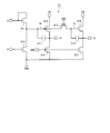
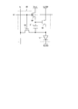
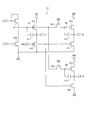
- FIG. 2 is a circuit diagram of a pixel circuit of the display device shown in FIG. 1.
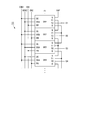
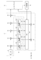
- FIG. 2 is a block diagram of a scanning line driving circuit of the display device shown in FIG. 1.
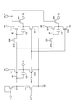
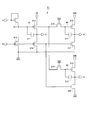
- FIG. 4 is a circuit diagram of a unit circuit of the scanning line driving circuit shown in FIG. 3.
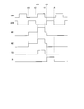
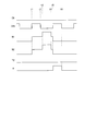
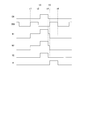
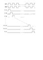
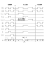
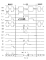
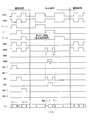
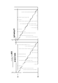
- 5 is a timing chart of the unit circuit shown in FIG. 5 is a timing chart of the unit circuit shown in FIG. 5 is a timing chart of the unit circuit shown in FIG. 5 is a timing chart of the unit circuit shown in FIG. 3 is a timing chart illustrating an operation of the display device illustrated in FIG. 1.
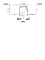
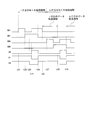
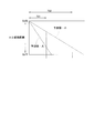
- FIG. 2 is a timing chart showing a waveform of an output signal Y1 during a pause period of the display device shown in FIG. It is a schematic diagram which shows the change of the voltage of a data line and a monitor line in the idle period of the display apparatus shown in FIG. It is a detailed timing chart of the display apparatus shown in FIG. It is a block diagram which shows the detail of the correction data memory
- FIG. 16 is a circuit diagram of a pixel circuit of the display device shown in FIG. 15.
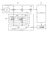
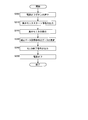
- FIG. 16 is a block diagram illustrating details of a correction data storage unit and a correction calculation unit of the display device illustrated in FIG. 15. It is a flowchart which shows operation
- FIG. 21 is a circuit diagram of a pixel circuit of the display device shown in FIG. 20.
- FIG. 21 is a block diagram of a scanning line driving circuit of the display device shown in FIG. 20.
- FIG. 23 is a circuit diagram of a unit circuit of the scanning line driving circuit shown in FIG. 22. It is a detailed timing chart of the display apparatus shown in FIG. FIG.
- FIG. 21 is a schematic diagram illustrating a change in voltage of a data line during a pause period of the display device illustrated in FIG. 20. It is a timing chart for demonstrating the drive method in the 4th Embodiment of this invention. It is a block diagram which shows the structure of the display apparatus which concerns on the 5th Embodiment of this invention. In the said 5th Embodiment, it is a circuit diagram which shows the structure of the area
- FIG. 10 is a diagram for describing switching of data line connection destinations in the first modified example.
- FIG. 10 is a figure which shows one structural example of a voltage measurement part. It is a detailed timing chart of the display apparatus shown in FIG.
- a 2nd modification it is a circuit diagram which shows the structure of a pixel circuit and a current measurement part. It is a figure for demonstrating control of a control clock signal in the said 2nd modification. In the said 2nd modification, it is a figure for demonstrating adjustment of integration time. It is a block diagram which shows the structure of the display apparatus which concerns on a 3rd modification. It is a circuit diagram of a unit circuit in the scanning line driving circuit in the third modification. It is a timing chart for demonstrating the drive method of the scanning line in the said 3rd modification. It is a block diagram which shows the structure of the principal part of the unit circuit in a 4th modification. It is a circuit diagram of a unit circuit in the fourth modification.
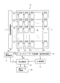
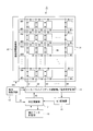
- FIG. 1 is a block diagram showing a configuration of a display device according to the first embodiment of the present invention.
- 1 includes a display unit 11, a display control circuit 12, a scanning line driving circuit 13, a source driver (data line driving / current measuring circuit) 14, an A / D converter 15, a correction data storage unit 16,
- the active matrix organic EL display device includes the correction calculation unit 17.
- m and n are integers of 2 or more, i is an integer of 1 to n, and j is an integer of 1 to m.
- the display unit 11 includes n scanning lines G1 to Gn, m data lines S1 to Sm, m monitor lines M1 to Mm, and (m ⁇ n) pixel circuits 18.
- the scanning lines G1 to Gn are arranged in parallel to each other.
- the data lines S1 to Sm and the monitor lines M1 to Mm are arranged in parallel to each other and orthogonal to the scanning lines G1 to Gn.
- the scanning lines G1 to Gn and the data lines S1 to Sm intersect at (m ⁇ n) locations.
- the (m ⁇ n) pixel circuits 18 are two-dimensionally arranged corresponding to the intersections of the scanning lines G1 to Gn and the data lines S1 to Sm.
- the (m ⁇ n) pixel circuits 18 form a pixel matrix of n rows ⁇ m columns.
- the pixel circuit 18 is supplied with a high level power supply voltage ELVDD and a low level power supply voltage ELVSS using electrodes (not shown).
- ELVDD high level power supply voltage
- ELVSS low level power supply voltage
- the extending direction of the scanning lines horizontal direction in FIG. 1
- the extending direction of the data lines vertical direction in FIG. 1
- the display control circuit 12 is a control circuit of the display device 1.
- the display control circuit 12 outputs a control signal CS1 to the scanning line driving circuit 13, outputs a control signal CS2 to the source driver 14, and outputs a video signal X1 to the correction calculation unit 17.
- the control signal CS2 includes, for example, a source start pulse and a source clock. Details of the control signal CS1 will be described later.
- the scanning line driving circuit 13 drives the scanning lines G1 to Gn according to the control signal CS1 (details will be described later). Note that the scanning line driving circuit 13 is supplied with a high level voltage VDD and a low level voltage VSS from a power supply circuit (not shown).
- the source driver 14 is supplied with the control signal CS2 and the corrected video signal X2 output from the correction calculation unit 17.
- the source driver 14 has a function of driving the data lines S1 to Sm (function as a data line drive circuit) and a function of measuring currents output from the pixel circuit 18 to the monitor lines M1 to Mm (function as a current measurement circuit). ).
- the source driver 14 applies m voltages (hereinafter referred to as data voltages) corresponding to the video signal X2 to the data lines S1 to Sm according to the control signal CS2.
- the source driver 14 applies m measurement voltages to the data lines S1 to Sm according to the control signal CS2, respectively, and outputs m currents output from the pixel circuit 18 to the monitor lines M1 to Mm at that time. Each is converted to voltage and output.
- the A / D converter 15 converts the output voltage of the source driver 14 into digital data.
- the correction data storage unit 16 stores data necessary for correction calculation by the correction calculation unit 17 (hereinafter referred to as correction data).
- the correction calculation unit 17 updates the correction data stored in the correction data storage unit 16 based on the data output from the A / D converter 15.
- the correction calculation unit 17 refers to the correction data stored in the correction data storage unit 16, corrects the video signal X1 output from the display control circuit 12, and outputs a corrected video signal X2.
- FIG. 2 is a circuit diagram of the pixel circuit 18 in the i-th row and j-th column.
- the pixel circuit 18 includes an organic EL element L1, transistors Q1 to Q3, and a capacitor C1, and is connected to the scanning line Gi, the data line Sj, and the monitor line Mj.
- the transistors Q1 to Q3 are N-channel TFTs (Thin Film Transistor).
- the high level power supply voltage ELVDD is applied to the drain terminal of the transistor Q1.
- the source terminal of the transistor Q1 is connected to the anode terminal of the organic EL element L1.
- a low level power supply voltage ELVSS is applied to the cathode terminal of the organic EL element L1.
- One conduction terminal left terminal in FIG.
- the transistor Q2 is connected to the data line Sj, and the other conduction terminal of the transistor Q2 is connected to the gate terminal of the transistor Q1.
- One conduction terminal (left terminal in FIG. 2) of the transistor Q3 is connected to the monitor line Mj, and the other conduction terminal of the transistor Q3 is connected to the source terminal of the transistor Q1 and the anode terminal of the organic EL element L1.
- the gate terminals of the transistors Q2 and Q3 are connected to the scanning line Gi.
- the capacitor C1 is provided between the gate terminal and the source terminal of the transistor Q1.
- the transistor Q1 functions as a drive transistor
- the transistor Q2 functions as a write control transistor
- the transistor Q3 functions as a read control transistor.
- FIG. 3 is a block diagram showing a configuration of the scanning line driving circuit 13.
- the scanning line driving circuit 13 includes a shift register in which n unit circuits 41 are connected in multiple stages.
- FIG. 3 shows the unit circuits 41 in the first to fourth stages, but the unit circuits 41 in the fifth to nth stages are connected in the same manner.
- the unit circuit 41 has clock terminals CK and CKB, an enable terminal EN, a set terminal S, a reset terminal R, and output terminals Y1 and Y2.
- the control signal CS1 supplied to the scanning line driving circuit 13 includes a gate start pulse GSP, gate clocks GCK1, GCK2, and enable signals EN1, EN2.
- the gate start pulse GSP is given to the set terminal S of the unit circuit 41 in the first stage.
- the gate clock GCK1 is supplied to the clock terminal CK of the odd-numbered unit circuit 41 and the clock terminal CKB of the even-numbered unit circuit 41.
- the gate clock GCK2 is supplied to the clock terminal CK of the even-numbered unit circuit 41 and the clock terminal CKB of the odd-numbered unit circuit 41.
- the enable signal EN1 is applied to the enable terminal EN of the odd-numbered unit circuit 41, and the enable signal EN2 is applied to the enable terminal EN of the even-numbered unit circuit 41.
- the output terminal Y1 of the first stage unit circuit 41 is connected to the set terminal S of the second stage unit circuit 41.
- the output terminal Y1 of the second to (n-1) th stage unit circuits 41 is connected to the set terminal S of the next stage unit circuit 41 and the reset terminal R of the previous stage unit circuit 41.
- the output terminal Y1 of the n-th unit circuit 41 is connected to the reset terminal R of the (n ⁇ 1) -th unit circuit 41.
- a signal indicating the end of the video signal period is supplied to the reset terminal R of the n-th unit circuit 41 (not shown).
- the output terminal Y2 of the i-th unit circuit 41 is connected to the scanning line Gi.
- FIG. 4 is a circuit diagram of the unit circuit 41.
- the unit circuit 41 includes transistors Q11 to Q17 and capacitors C11 and C12.
- Transistors Q11 to Q17 are N-channel TFTs.
- the drain terminal and gate terminal of the transistor Q11 are connected to the set terminal S.
- the source terminal of the transistor Q11 is connected to the drain terminal of the transistor Q12, the gate terminal of the transistor Q13, and one conduction terminal (the left terminal in FIG. 4) of the transistor Q15.
- the drain terminal of the transistor Q13 is connected to the clock terminal CK, and the source terminal of the transistor Q13 is connected to the drain terminal of the transistor Q14 and the output terminal Y1.
- the other conduction terminal of the transistor Q15 is connected to the gate terminal of the transistor Q16, and the high level voltage VDD is applied to the gate terminal of the transistor Q15.
- the drain terminal of the transistor Q16 is connected to the enable terminal EN, and the source terminal of the transistor Q16 is connected to the drain terminal of the transistor Q17 and the output terminal Y2.
- a low level voltage VSS is applied to the source terminals of the transistors Q12, Q14, and Q17.
- the gate terminal of the transistor Q12 is connected to the reset terminal R, and the gate terminals of the transistors Q14 and Q17 are connected to the clock terminal CKB.
- the capacitor C11 is provided between the gate terminal and the source terminal of the transistor Q13, and the capacitor C12 is provided between the gate terminal and the source terminal of the transistor Q16.
- the transistors Q11 and Q12 function as a node control circuit that switches the voltage of the node N1 (first node) shown in FIG. 4 between a high level and a low level in accordance with signals input from the set terminal S and the reset terminal R.
- the transistors Q13 and Q14 and the capacitor C11 apply a signal input from the clock terminal CK to the set terminal S of the next unit circuit 41 and the reset terminal R of the previous unit circuit 41 when the node N1 is in the boost state. It functions as a first output control circuit.
- the transistors Q15 to Q17 and the capacitor C12 function as a second output control circuit that applies the enable signal EN1 or EN2 output from the display control circuit 12 to the scanning line Gi when the voltage of the node N1 is at a high level.
- the transistors Q1 to Q3 included in the pixel circuit 18 and the transistors Q11 to Q17 included in the unit circuit 41 of the scanning line driving circuit 13 are, for example, indium (In), gallium (Ga), zinc (Zn), and An oxide semiconductor containing oxygen (O) is used.
- FIG. 5 is a timing chart of the unit circuit 41.
- a signal input / output via the terminal of the unit circuit 41 is referred to by the same name as that terminal.
- a signal input via the clock terminal CK is referred to as a clock signal CK.
- the nodes to which the gate terminals of the transistors Q13 and Q16 are connected are referred to as a node N1 and a node N2, respectively.
- the clock signals CK and CKB are at a high level in different periods.
- the set signal S becomes high level during the high level period of the clock signal CKB (time t1 to t2 in FIG. 5).
- the reset signal R becomes high level in the next high level period (time t5 to t6 in FIG. 5) of the clock signal CKB.
- the voltage of the node N1 Prior to time t1, the voltage of the node N1 is at a low level.
- the transistor Q11 When the set signal S changes to high level at time t1, the transistor Q11 is turned on, and the voltage at the node N1 changes to high level. Note that when the voltage at the node N1 is a normal high level, the transistor Q13 is turned on. However, since the clock signal CK is at a low level, the output signal Y1 is maintained at a low level.
- the transistor Q11 When the set signal S changes to the low level at time t2, the transistor Q11 is turned off and the node N1 enters a high impedance state. The voltage at the node N1 remains high after time t2.
- the clock signal CK changes to high level.
- the voltage of the node N1 becomes higher than a normal high level by bootstrap (the node N1 is in a boost state). Therefore, the high-level clock signal CK is output from the output terminal Y1 through the transistor Q13 at the same level (without decreasing by the threshold voltage of the transistor Q13).
- the clock signal CK changes to low level at time t4
- the voltage at the node N1 returns to normal high level, and the output signal Y1 changes to low level.
- the transistor Q12 When the reset signal R changes to high level at time t5, the transistor Q12 is turned on, and the voltage at the node N1 changes to low level. Further, when the clock signal CKB changes to a high level at time t5, the transistor Q14 is turned on. The transistor Q14 has a function of reliably setting the output signal Y1 to a low level. Thus, when the voltage of the node N1 is at a high level, the clock signal CK is output from the output terminal Y1.
- Transistors Q16 and Q17 and capacitor C12 are connected in the same manner as transistors Q13 and Q14 and capacitor C11.
- the enable signal EN changes to a high level when the node N2 is in a high impedance state and the voltage at the node N2 is at a high level
- the voltage at the node N2 becomes higher than a normal high level by bootstrap (the node N2 is in a boost state) Becomes).
- the transistor Q15 is kept on except when the voltage at the node N2 is higher than the normal high level.
- Node N2 has a voltage of the same logic level as node N1. Therefore, the enable signal EN is output from the output terminal Y2 when the voltages at the nodes N1 and N2 are at a high level.
- the transistor Q15 is turned off when the voltage of the node N2 exceeds a predetermined level, and has a function of electrically disconnecting the nodes N1 and N2 and assisting the increase in the voltage of the node N2 due to bootstrap.
- Capacitor C11 has a function of assisting the rise in voltage of node N1 due to bootstrap and a function of reducing the influence of noise mixed in clock signal CK on the voltage of node N1 through the parasitic capacitance of transistor Q13.
- the capacitor C12 has the same function as the capacitor C11.
- the node N2 has the same logic level voltage as the node N1.
- the enable signal EN having the waveform shown in FIG.
- the voltage of the node N2 becomes higher than the normal high level by bootstrap (the node N2 is in a boost state).
- the high level enable signal EN is output at the output terminal Y2 through the transistor Q16 at the same level (without decreasing by the threshold voltage of the transistor Q16) (see FIG. 6).
- the enable signal EN is maintained at a low level as shown in FIG. 7 except for a current measurement period described later.
- the enable signal EN becomes high level only during the current measurement period. Therefore, during the current measurement period (the period from time t3 to time t4 in FIG. 8), the voltage at the node N2 becomes higher than the normal high level by bootstrap, so that the high level enable signal EN remains unchanged.
- the signal passes through the transistor Q16 and is output from the output terminal Y2.
- FIG. 9 is a timing chart showing the operation of the display device 1.
- the display device 1 performs pause driving using a driving period and a pause period.
- the length of the driving period is set to one frame period, and the driving period is divided into a video signal period and a vertical blanking period.
- the video signal period includes n line periods (also called horizontal periods) corresponding to the n rows of pixel circuits 18.
- the periods of the gate clocks GCK1 and GCK2 are each two line periods, and the n scanning lines G1 to Gn are sequentially selected one line period at a time.
- the scanning line driving circuit 13 controls the voltage of the scanning line Gi to a high level, and the source driver 14 applies m data voltages to the data lines S1 to Sm.
- the data voltage is written in the m pixel circuits 18 connected to the scanning line Gi (described as a program in FIG. 9).
- the length of the pause period is longer than one frame period, and is set to a plurality of frame periods, for example.
- the pause period is divided into a video holding period and a vertical blanking period.
- the gate clocks GCK1 and GCK2 change between a high level and a low level not only in the driving period but also in the rest period.
- the period of the gate clocks GCK1 and GCK2 in the idle period is longer than the two-line period.
- the output signal Y1 of the n unit circuits 41 is a half cycle of the gate clocks GCK1, GCK2 in ascending order (in the order of the first stage, the second stage, the third stage,). Each level goes high.
- the periods in which the output signal Y1 of the unit circuits 41 in the 1st to nth stages in the idle period is at the high level are referred to as the 1st to nth idle line periods, respectively.
- the video holding period includes the 1st to nth pause line periods once.
- one idle line period (hereinafter referred to as i-th idle line period) is selected as the current measurement period.
- the scanning line Gi is selected during the current measurement period.
- the scanning line driving circuit 13 applies a scanning signal for current measurement and a scanning signal for voltage writing to the selected scanning line Gi during the current measurement period.
- the scanning line selected in the pause period is determined by a predetermined method (for example, in ascending order or randomly), and is switched every four pause periods.
- the scanning line driving circuit 13 controls the voltages of the scanning lines G1 to Gn to a low level (shown by thick broken lines in FIG. 9).
- FIG. 11 is a schematic diagram showing changes in the voltage of the data line Sj and the monitor line Mj during the pause period.
- the source driver 14 applies measurement voltages to the data lines S1 to Sm, measures the output currents output from the m pixel circuits 18 to the monitor lines M1 to Mm, M data voltages are applied to the data lines S1 to Sm.
- a process for writing a measurement voltage, a process for measuring a current, and a process for writing a data voltage are performed.
- the process of writing the measurement voltage and the process of measuring the current are performed in the same time zone.
- the source driver 14 does not drive the data line Sj during a period other than the current measurement period during the pause period.
- FIG. 12 is a detailed timing chart of the display device 1.
- FIG. 12 shows the timing when the even-numbered scanning line Gi (i is an even number) is selected in the pause period. Note that some intervals are provided between the falling time of one clock and the rising time of the other clock as shown in FIG. 5, but in FIG. 12, for convenience of explanation, this interval is ignored. It is shown.
- the gate clocks GCK1 and GCK2 are at a high level in different periods. In the driving period, the period of the gate clocks GCK1 and GCK2 is a two-line period, and the gate start pulse GSP (not shown) becomes high level for one line period before the start of the driving period.
- the output signal Y1 of the unit circuits 41 at the 1st to nth stages is at the high level during the 1st to nth line periods, and is at the low level during the other periods in the driving period.
- the enable signals EN1 and EN2 change in the same manner as the gate clocks GCK1 and GCK2, respectively.
- the clock signal CK and the enable signal EN change similarly, and the output signal Y2 changes similarly to the output signal Y1. Therefore, during the driving period, the voltages of the scanning lines G1 to Gn are at a high level only in the 1st to nth line periods, respectively.
- the periods of the gate clocks GCK1 and GCK2 are each 2 idle line periods, and the gate start pulse GSP becomes high level only for one idle line period at a predetermined timing within the idle period. Therefore, the output signal Y1 of the unit circuits 41 in the 1st to n-th stages is at a high level during the i-th pause line period, and is at a low level during other periods in the pause period.
- the enable signal EN1 is at a high level when i is an odd number during the i-th idle line period, and the enable signal EN2 when i is an even number. Becomes high level.
- the enable signals EN1 and EN2 are at a low level during other periods within the pause period (FIG. 12 shows a case where i is an even number). Therefore, in the unit circuit 41 at the i-th stage, the clock signal CK and the enable signal EN change similarly, and the output signal Y2 changes similarly to the output signal Y1. In the unit circuits 41 at the 1st to nth stages (excluding the i-th stage), the enable signal EN is at a low level, so the output signal Y2 is at a low level. Therefore, during the idle period, the voltage of the scanning line Gi is high only during the i-th idle line period, and the voltages of the scanning lines G1 to Gn (except for Gi) are maintained at low level.
- the characteristics of the transistor Q1 are referred to as “TFT characteristics”, and the characteristics of the organic EL element L1 are referred to as “OLED characteristics”.
- TFT characteristics the characteristics of the transistor Q1
- OLED characteristics the characteristics of the organic EL element L1
- the source driver 14 applies the data voltage Dij to the data line Sj. Therefore, the gate voltage of the transistor Q1 is Dij.
- the voltage of the selected scanning line Gi changes to a low level. Accordingly, the transistors Q2 and Q3 are turned off. Thereafter, the gate voltage of the transistor Q1 is kept at Dij by the action of the capacitor C1.
- the transistor Q1 is turned on, and an amount of current corresponding to the gate-source voltage of the transistor Q1 flows through the organic EL element L1.
- the organic EL element L1 emits light with a luminance corresponding to the amount of flowing current.
- the voltage of the selected scanning line Gi changes to a high level. Accordingly, the transistors Q2 and Q3 are turned on.
- the source driver 14 applies the measurement voltage Vmg (i, j) to the data line Sj. Therefore, the gate voltage of the transistor Q1 is Vmg (i, j).
- the measurement voltage Vmg (i, j) is either a TFT characteristic measurement voltage or an OLED characteristic measurement voltage. Note that the value of the measurement voltage Vmg (i, j) is set such that current flows only through either the transistor Q1 or the organic EL element L1 during the current measurement period.
- the measurement voltage Vmg (i, j) when the OLED characteristic is measured is an arbitrary voltage that does not turn on the transistor Q1. Further, when applying the OLED characteristic measurement voltage to the data line Sj, the source driver 14 further applies a voltage Vm (i, j) for causing a current to flow through the organic EL element L1 to the monitor line Mj. . When the TFT characteristic measurement voltage is applied, the transistor Q1 is turned on, and a current passing through the transistors Q1 and Q3 flows from the electrode having the high level power supply voltage ELVDD to the monitor line Mj.
- the transistor Q1 When the voltage for measuring OLED characteristics is applied, the transistor Q1 is turned off, and a current passing through the transistor Q3 and the organic EL element L1 from the monitor line Mj flows to the electrode having the low level power supply voltage ELVSS.
- the source driver 14 measures the current flowing through the monitor line Mj in the first half of the i-th pause line period.
- the source driver 14 applies the data voltage Dij to the data line Sj.
- the pixel circuit 18 operates in the same manner as in the i-th line period.
- the voltage of the scanning line Gi changes to a low level.
- the organic EL element L1 emits light with a luminance corresponding to the data voltage Dij.
- FIG. 13 is a block diagram showing details of the correction data storage unit 16 and the correction calculation unit 17.
- the correction data storage unit 16 includes a TFT gain storage unit 16a, an OLED gain storage unit 16b, a TFT offset storage unit 16c, and an OLED offset storage unit 16d.
- the four storage units 16a to 16d store (m ⁇ n) correction data corresponding to (m ⁇ n) pixel circuits 18, respectively.
- the TFT gain storage unit 16a stores a gain based on the detection result of the TFT characteristics (hereinafter referred to as TFT gain).
- the OLED gain storage unit 16b stores a gain based on the detection result of the OLED characteristic (hereinafter referred to as OLED gain).
- the TFT offset storage unit 16c stores an offset (hereinafter referred to as a TFT offset) based on the detection result of the TFT characteristics.
- the OLED offset storage unit 16d stores an offset based on the detection result of the OLED characteristic (hereinafter referred to as an OLED offset).
- the correction calculation unit 17 includes an LUT 61, multipliers 62, 63, 66 and 67, adders 64, 65 and 68, and a CPU 69.
- the correction calculation unit 17 receives the gradation P included in the video signal X1, the gradation P for detecting TFT characteristics, the value pre_Vmg_oled for detecting OLED characteristics, and the output of the A / D converter 15. From the four storage units 16a to 16d, correction data of the pixel circuit 18 in the i-th row and j-th column is read out.
- the LUT 61 performs gamma correction on the gradation P.
- the multiplier 62 multiplies the output of the LUT 61 by the TFT gain read from the TFT gain storage unit 16a.
- the multiplier 63 multiplies the output of the multiplier 62 by the OLED gain read from the OLED gain storage unit 16b.
- the adder 64 adds the TFT offset read from the TFT offset storage unit 16 c to the output of the multiplier 63.
- the adder 65 adds the OLED offset read from the OLED offset storage unit 16 d to the output of the adder 64.
- the multiplier 66 multiplies the output of the adder 65 by a coefficient Z for compensating for the attenuation of the data voltage.
- the correction calculation unit 17 outputs the video signal X2 including the output of the multiplier 66 to the source driver 14 during the video signal period.
- the correction calculation unit 17 outputs the output of the multiplier 66 as data corresponding to the measurement voltage Vmg (i, j) to the source driver 14 during the current measurement period in which the TFT characteristics are detected.
- the multiplier 67 multiplies the value pre_Vmg_oled by the OLED gain read from the OLED gain storage unit 16b.
- the adder 68 adds the OLED offset read from the OLED offset storage unit 16 d to the output of the multiplier 67.
- the correction calculation unit 17 outputs the output of the adder 68 to the voltage (voltage for flowing current through the organic EL element L1) Vm (i, j) to the source driver 14. Output as corresponding data.
- FIG. 14 is a flowchart showing the operation of the CPU 69.
- the CPU 69 executes steps S101 to S116 shown in FIG. 14 every four pause periods.
- the CPU 69 executes steps S101 to S104 during the first suspension period, executes steps S105 to S108 during the second suspension period, executes steps S109 to S112 during the third suspension period, and performs the steps during the fourth suspension period. Executes steps S113 to S116.
- the source driver 14 applies the first measurement voltage Vmg (i, j) for measuring the TFT characteristics to the data lines S1 to Sm in the first half of the current measurement period within the first pause period. Currents output from the pixel circuit 18 to the monitor lines M1 to Mm are measured.
- the CPU 69 receives the first current measurement value obtained at this time from the A / D converter 15 (step S101). Next, the CPU 69 obtains a first TFT characteristic based on the first current measurement value received in step S101 (step S102). Next, the CPU 69 updates the TFT offset stored in the TFT offset storage unit 16c using the first TFT characteristics (step S103), and sets the TFT gain stored in the TFT gain storage unit 16a. Update (step S104).
- the source driver 14 applies the second measurement voltage Vmg (i, j) for measuring the TFT characteristics to the data lines S1 to Sm in the first half of the current measurement period within the second pause period.
- Currents output from the pixel circuit 18 to the monitor lines M1 to Mm are measured.
- the CPU 69 receives the second current measurement value obtained at this time from the A / D converter 15 (step S105).
- the CPU 69 obtains a second TFT characteristic based on the second current measurement value received in step S105 (step S106).
- the CPU 69 updates the TFT offset stored in the TFT offset storage unit 16c using the second TFT characteristics (step S107), and sets the TFT gain stored in the TFT gain storage unit 16a. Update (step S108).
- the first measurement voltage and the second measurement voltage are different from each other.
- the first measurement voltage is a data voltage corresponding to a relatively low gradation
- the second measurement voltage is a data voltage corresponding to a relatively high gradation.
- the source driver 14 applies the third measurement for measuring the OLED characteristics while applying a voltage to the data lines S1 to Sm so that the transistor Q1 is not turned on in the first half of the current measurement period within the third pause period.
- the application voltage Vm (i, j) is applied to the monitor lines M1 to Mm, and currents output from the pixel circuit 18 to the monitor lines M1 to Mm at this time are measured.
- the CPU 69 receives the third current measurement value obtained at this time from the A / D converter 15 (step S109). Next, the CPU 69 obtains a first OLED characteristic based on the third current measurement value received in step S109 (step S110). Next, the CPU 69 updates the OLED offset stored in the OLED offset storage unit 16d by using the first OLED characteristic (step S111), and sets the OLED gain stored in the OLED gain storage unit 16b. Update (step S112).
- the source driver 14 applies a voltage that does not turn on the transistor Q1 to the data lines S1 to Sm, and performs the fourth measurement for measuring the OLED characteristics.
- the application voltage Vm (i, j) is applied to the monitor lines M1 to Mm, and currents output from the pixel circuit 18 to the monitor lines M1 to Mm at this time are measured.
- the CPU 69 receives the fourth current value obtained at this time from the A / D converter 15 (step S113). Next, the CPU 69 obtains a second OLED characteristic based on the fourth current measurement value received in step S113 (step S114).
- the CPU 69 updates the OLED offset stored in the OLED offset storage unit 16d using the second OLED characteristic (step S115), and sets the OLED gain stored in the OLED gain storage unit 16b. Update (step S116). Note that the third measurement voltage and the fourth measurement voltage are different from each other.
- the display control circuit 12 switches the pause line period in which the high level enable signals EN1 and EN2 are output during the pause period every four pause periods. Accordingly, the scanning line selected in the pause period is switched every four pause periods.
- the source driver 14 measures the current output from the pixel circuit 18 to which the first to fourth measurement voltages are written during the first to fourth rest periods, respectively.
- the correction calculation unit 17 updates the correction data stored in the correction data storage unit 16 based on the first to fourth current measurement values in the first to fourth pause periods, respectively.
- the display device 1 is two-dimensionally arranged with n scanning lines G1 to Gn, m data lines S1 to Sm, and m monitor lines M1 to Mm.
- a display unit 11 including (m ⁇ n) pixel circuits 18, a display control circuit 12, a scanning line driving circuit 13, and a source driver 14 are provided.
- the scanning line driving circuit 13 sequentially selects the scanning lines G1 to Gn for each line period, and applies a high level (selection level) scanning signal to the selected scanning line.
- the scanning line driving circuit 13 is also at a high level (for current measurement and voltage writing) with respect to the scanning line Gi selected from the scanning lines G1 to Gn during the current measurement period set within the pause period.
- a scan signal is applied, and a scan signal at a low level (non-selection level) is applied to the scan lines G1 to Gn in a period other than the current measurement period within the pause period.
- the source driver 14 applies a data voltage corresponding to the video signal X2 to the data lines S1 to Sm for each line period.
- the source driver 14 also applies a measurement voltage to the data lines S1 to Sm during the current measurement period, measures the current output from the pixel circuit 18 to the monitor lines M1 to Mm, and determines the data lines S1 to Sm. A data voltage is applied to Sm.
- the display device 1 when the rest drive is performed using the drive period and the rest period, the current measurement period is set within the rest period, and the measurement voltage is written in the current measurement period.
- the current output from the pixel circuit 18 can be measured.
- the power consumption of the display device 1 can be reduced by fixing the voltages of the scanning lines G1 to Gn in a period other than the current measurement period within the idle period.
- the display control circuit 12 outputs two enable signals EN1 and EN2 that alternately become high level for each line period during the driving period, and one becomes high level during the current measurement period during the rest period.
- the scanning line driving circuit 13 has a plurality of unit circuits 41 (a plurality of stages) corresponding to the scanning lines G1 to Gn, and shifts to output scanning signals to be applied to the scanning lines G1 to Gn based on the enable signals EN1 and EN2. Contains registers. Based on the enable signals EN1 and EN2 that change in different manners between the driving period and the rest period, the scanning signal for the driving period and the scanning signal for the rest period are generated using the same shift register. The configuration can be simplified.
- the unit circuit 41 (each stage of the shift register) includes a node control circuit (transistors Q11 and Q12), a first output control circuit (transistors Q13 and Q14 and a capacitor C11), and a second output control circuit (transistors Q15 to Q17). Capacitor C12). In this way, using two output control circuits, a scanning signal based on the enable signal EN1 or EN2 can be output separately from the output signal to the unit circuit 41 in the next stage.
- the first output control circuit includes a drain terminal (first conduction terminal) connected to the clock terminal CK, a source terminal (second conduction terminal) connected to the next stage set terminal S and the previous stage reset terminal R, A transistor Q13 (first output control transistor) having a gate terminal (control terminal) connected to the node N1, a drain terminal connected to the next set terminal S and the previous reset terminal R, and a low level voltage VSS A transistor Q11 having a source terminal to be applied and a gate terminal connected to the clock terminal CKB, and a capacitor C11 provided between the gate terminal and the source terminal of the transistor Q13 can be used.
- the second output control circuit is connected to the drain terminal to which the enable signal EN1 or EN2 is applied, the source terminal connected to the scanning line Gi, and the node N2 (second node) having the same logic level voltage as the node N1.
- a transistor Q16 having a gate terminal (second output control transistor), a drain terminal connected to the scanning line Gi, a source terminal to which a low level voltage VSS is applied, and a gate terminal connected to the clock terminal CKB.
- the pixel circuit 18 is provided between the organic EL element L1 (electro-optical element), the transistor Q1 (driving transistor) provided in series with the organic EL element L1, and the data line Sj and the gate terminal of the transistor Q1 for scanning.
- a transistor Q2 write control transistor having a gate terminal connected to the line Gi and a gate terminal provided between the monitor line Mj and the source terminal (one conduction terminal) of the transistor Q1 and connected to the scanning line Gi And a capacitor C1 provided between the gate terminal and the source terminal of the transistor Q1.
- the current of the pixel circuit is measured using a simple circuit while preventing deterioration of the image quality of the display image. can do.
- the display control circuit 12 receives an enable signal EN1 for the odd-numbered unit circuit 41 (odd-numbered stage of the shift register) and an enable signal EN2 for the even-numbered unit circuit 41 (even-numbered stage of the shift register). Output. In this way, by supplying different enable signals to the odd and even stages of the shift register, it is possible to prevent the voltages of the adjacent scanning lines from becoming high level in the same time zone.
- an oxide semiconductor containing indium, gallium, zinc, and oxygen has higher mobility than amorphous silicon. Therefore, by forming the transistors Q11 to Q17 included in the scan line driver circuit 13 using the oxide semiconductor, the size of the transistors can be reduced and the layout area of the scan line driver circuit 13 can be reduced. . Therefore, when the pixel circuit 18 and the scanning line driving circuit 13 are integrally formed (also referred to as a gate driver monolithic configuration), the frame area formed around the pixel region can be reduced. In addition, a transistor formed using the above oxide semiconductor has a feature of low off-leakage current.
- the shift register included in the scanning line driving circuit 13 performs a shift operation for each line period in the drive period, and performs a shift operation for each idle line period longer than the line period in the idle period.
- the display device 1 further includes a correction calculation unit 17 that corrects the video signal X1 based on the current measured by the source driver 14. Therefore, by correcting the video signal X1 based on the current measurement result, it is possible to compensate for the decrease in luminance of the pixel and improve the image quality of the display image.
- FIG. 15 is a block diagram showing a configuration of a display device according to the second embodiment of the present invention.
- the display device 2 shown in FIG. 15 is the same as the display device 1 according to the first embodiment, except that the display unit 11, the correction data storage unit 16, and the correction calculation unit 17 are the display unit 21 and the correction data storage unit 26, respectively. , And the correction calculation unit 27.
- the display device 2 has a feature that a data line and a monitor line are shared.
- the same elements as those of the first embodiment are denoted by the same reference numerals and description thereof is omitted.
- the display unit 21 includes n scanning lines G1 to Gn, m data lines S1 to Sm, and (m ⁇ n) pixel circuits 28.
- the scanning lines G1 to Gn are arranged in parallel to each other.
- the data lines S1 to Sm are arranged in parallel to each other and orthogonal to the scanning lines G1 to Gn.
- the (m ⁇ n) pixel circuits 28 are two-dimensionally arranged corresponding to the intersections of the scanning lines G1 to Gn and the data lines S1 to Sm.
- the pixel circuit 28 is supplied with a reference voltage Vref using a wiring (not shown).
- FIG. 16 is a circuit diagram of the pixel circuit 28 in the i-th row and j-th column.
- the pixel circuit 28 includes an organic EL element L1, transistors Q1 to Q3, and a capacitor C1, and is connected to the scanning line Gi and the data line Sj.
- the transistor Q1 and the organic EL element L1 are connected in the same manner as the pixel circuit 18.
- One conduction terminal (left terminal in FIG. 16) of the transistor Q2 is connected to the data line Sj, and the other conduction terminal of the transistor Q2 is connected to the source terminal of the transistor Q1 and the anode terminal of the organic EL element L1.
- the drain terminal of the transistor Q3 is connected to the wiring having the reference voltage Vref, and the source terminal of the transistor Q3 is connected to the gate terminal of the transistor Q1.
- the gate terminals of the transistors Q2 and Q3 are connected to the scanning line Gi.
- the capacitor C1 is provided between the gate terminal and the source terminal of the transistor Q1.
- the transistor Q1 functions as a drive transistor, the transistor Q2 functions as a write control transistor, and the transistor Q3 functions as a reference voltage application transistor.
- FIG. 17 is a detailed timing chart of the display device 2.
- the timing chart shown in FIG. 17 is obtained by deleting the voltage change of the monitor line Mj from the timing chart shown in FIG.
- the display device 2 can drive the scanning lines G1 to Gn according to the timing shown in FIG. 17 using the scanning line driving circuit 13 shown in FIGS.
- the display control circuit 12 switches the pause line period for outputting the high level enable signals EN1 and EN2 every two pause periods. Therefore, the scanning line selected in the pause period is switched every two pause periods.
- the transistors Q2 and Q3 are turned on.
- the source driver 14 applies the data voltage Dij to the data line Sj. Therefore, the gate-source voltage of the transistor Q1 is (Vref-Dij).
- the voltage of the selected scanning line Gi changes to a low level. Accordingly, the transistors Q2 and Q3 are turned off. Thereafter, the gate-source voltage of the transistor Q1 is maintained at (Vref ⁇ Dij) by the action of the capacitor C1.
- the transistor Q1 is turned on, and a current corresponding to the gate-source voltage of the transistor Q1 flows through the organic EL element L1.
- the organic EL element L1 emits light with a luminance corresponding to the amount of flowing current.
- the source driver 14 applies the measurement voltage Vmg (i, j) to the data line Sj. Therefore, the gate-source voltage of the transistor Q1 is ⁇ Vref ⁇ Vmg (i, j) ⁇ . At this time, the transistor Q1 is turned on, and a current passing through the transistors Q1 and Q2 flows from the electrode having the high level power supply voltage ELVDD to the data line Sj. In a period T0 shown in FIG. 17, current flows through the data line Sj. The source driver 14 measures the current output to the data line Sj in the first half of the i-th idle line period.
- the source driver 14 applies the data voltage Dij to the data line Sj.
- the pixel circuit 28 operates in the same manner as in the i-th line period.
- the voltage of the scanning line Gi changes to a low level.
- the organic EL element L1 emits light with a luminance corresponding to the data voltage Dij.
- FIG. 18 is a block diagram showing details of the correction data storage unit 26 and the correction calculation unit 27.
- the correction data storage unit 26 includes a TFT gain storage unit 26a and a TFT offset storage unit 26b.
- the two storage units 26a and 26b store (m ⁇ n) correction data corresponding to (m ⁇ n) pixel circuits 28, respectively.
- the TFT gain storage unit 26a stores the TFT gain
- the TFT offset storage unit 26b stores the TFT offset.
- the correction calculation unit 27 includes an LUT 71, multipliers 72 and 74, an adder 73, and a CPU 75.
- the correction calculation unit 27 receives the gradation P included in the video signal X1, the gradation P for detecting TFT characteristics, and the output of the A / D converter 15.
- the correction data of the pixel circuit 28 in the i-th row and j-th column is read from the two storage units 26a and 26b.
- the LUT 71 performs gamma correction on the gradation P.
- the multiplier 72 multiplies the output of the LUT 71 by the TFT gain read from the TFT gain storage unit 26a.
- the adder 73 adds the TFT offset read from the TFT offset storage unit 26 b to the output of the multiplier 72.
- the multiplier 74 multiplies the output of the adder 73 by a coefficient Z for compensating for the attenuation of the data voltage.
- the correction calculator 27 outputs the video signal X2 including the output of the multiplier 74 to the source driver 14 during the video signal period.
- the correction calculation unit 27 outputs the output of the multiplier 74 to the source driver 14 as data corresponding to the measurement voltage Vmg (i, j) during the current measurement period.
- FIG. 19 is a flowchart showing the operation of the CPU 75.
- the CPU 75 executes steps S101 to S108 shown in FIG. 19 every two pause periods.
- the CPU 75 executes steps S101 to S104 during the first pause period and executes steps S105 to S108 during the second pause period.
- steps S101 to S108 the TFT offset stored in the TFT offset storage unit 26b is updated in steps S103 and S107, and the TFT gain stored in the TFT gain storage unit 26a is updated in steps S104 and S108.
- the second embodiment is the same as the first embodiment.
- the scanning line selected in the pause period is switched every two pause periods.
- the source driver 14 measures the current output from the pixel circuit 28 in which the first measurement voltage and the second measurement voltage are written in the first pause period and the second pause period, respectively.
- the correction calculation unit 27 updates the correction data stored in the correction data storage unit 26 based on the first current measurement value and the second current measurement value in the first pause period and the second pause period, respectively. .
- the display device 2 includes (m ⁇ n) pixel circuits arranged two-dimensionally with n scanning lines G1 to Gn and m data lines S1 to Sm. 28, the display control circuit 12, the scanning line driving circuit 13, and the source driver 14.
- the scanning line driving circuit 13 applies a high level (for current measurement and voltage writing) scanning signal to the scanning line Gi selected from the scanning lines G1 to Gn.
- the source driver 14 applies a measurement voltage to the data lines S1 to Sm, measures the current output from the pixel circuit 28 to the data lines S1 to Sm, and applies to the data lines S1 to Sm. In contrast, a data voltage is applied.
- the pixel circuit 28 includes an organic EL element L1 (electro-optical element), a transistor Q1 (driving transistor) provided in series with the organic EL element L1, a data line Sj, and a source terminal (one conduction terminal) of the transistor Q1.
- the transistor Q2 write control transistor
- the transistor Q3 reference voltage application transistor
- the transistor Q3 reference voltage application transistor
- the pixel circuit can be used while preventing deterioration in the image quality of a display image using a simple circuit.
- the current can be measured.
- FIG. 20 is a block diagram showing a configuration of a display device according to the third embodiment of the present invention.
- a display device 3 shown in FIG. 20 is obtained by replacing the display unit 11 and the scanning line driving circuit 13 with a display unit 31 and a scanning line driving circuit 33, respectively, in the display device 1 according to the first embodiment.
- the same elements as those of the first embodiment are denoted by the same reference numerals and description thereof is omitted.
- the display unit 31 includes 2n scanning lines GA1 to GAn, GB1 to GBn, m data lines S1 to Sm, and (m ⁇ n) pixel circuits 38.
- the scanning lines GA1 to GAn and GB1 to GBn are arranged in parallel to each other.
- the data lines S1 to Sm are arranged in parallel to each other and orthogonal to the scanning lines GA1 to GAn and GB1 to GBn.
- the (m ⁇ n) pixel circuits 38 are two-dimensionally arranged corresponding to the intersections of the scanning lines GA1 to GAn and the data lines S1 to Sm.
- the scanning lines GA1 to GAn correspond to the first scanning line
- the scanning lines GB1 to GBn correspond to the second scanning line.
- signals applied to the scanning lines GA1 to GAn correspond to the first scanning signal
- signals applied to the scanning lines GB1 to GBn correspond to the second scanning signal.
- FIG. 21 is a circuit diagram of the pixel circuit 38 in the i-th row and j-th column.
- the pixel circuit 38 includes an organic EL element L1, transistors Q1 to Q3, and a capacitor C1, and is connected to the scanning lines GAi and GBi and the data line Sj.
- the configuration of the pixel circuit 38 is the same as that of the pixel circuit 18 except for the following points.
- One conduction terminal (left terminal in FIG. 21) of the transistor Q3 is connected to the data line Sj.
- the gate terminals of the transistors Q2 and Q3 are connected to the scanning lines GAi and GBi, respectively.
- the capacitor C1 is provided between the gate terminal and the drain terminal of the transistor Q1.
- FIG. 22 is a block diagram showing a configuration of the scanning line driving circuit 33.
- the scanning line driving circuit 33 includes a shift register in which n unit circuits 51 are connected in multiple stages.
- the unit circuit 51 has clock terminals CK and CKB, enable terminals ENA and ENB, a set terminal S, a reset terminal R, and output terminals Y1 to Y3.
- the control signal CS1 supplied to the scanning line driving circuit 33 includes a gate start pulse GSP, gate clocks GCK1 and GCK2, and enable signals ENA1, ENA2, ENB1, and ENB2.
- the connection form of the unit circuit 51 is the same as the connection form of the unit circuit 41 according to the first embodiment except for the following points.
- the enable signals ENA1 and ENB1 are applied to enable terminals ENA and ENB of the odd-numbered unit circuits 51, respectively.
- the enable signals ENA2 and ENB2 are applied to the enable terminals ENA and ENB of the even-numbered unit circuit 51, respectively.
- the output terminals Y2 and Y3 of the i-th stage unit circuit 51 are connected to the scanning lines GAi and GBi, respectively.
- FIG. 23 is a circuit diagram of the unit circuit 51. As shown in FIG. 23, the unit circuit 51 is obtained by adding transistors Q18 to Q20, which are N-channel TFTs, and a capacitor C13 to the unit circuit 41. Transistors Q11 to Q17 and capacitors C11 and C12 are connected in the same manner as unit circuit 41. However, the drain terminal of the transistor Q16 is connected to the enable terminal ENA.
- One conduction terminal (left terminal in FIG. 23) of the transistor Q18 is connected to the node N1.
- the other conduction terminal of the transistor Q18 is connected to the gate terminal of the transistor Q19, and the high level voltage VDD is applied to the gate terminal of the transistor Q18.
- the drain terminal of the transistor Q19 is connected to the enable terminal ENB, and the source terminal of the transistor Q19 is connected to the drain terminal of the transistor Q20 and the output terminal Y3.
- the gate terminal of the transistor Q20 is connected to the clock terminal CKB, and the low level voltage VSS is applied to the source terminal of the transistor Q20.
- Capacitor C13 is provided between the gate terminal and source terminal of transistor Q19.
- the node to which the gate terminal of the transistor Q19 is connected is referred to as a node N3.
- Transistors Q11 and Q12 function as a node control circuit
- transistors Q13 and Q14 and capacitor C11 function as a first output control circuit.
- the transistors Q15 to Q20 and the capacitors C12 and C13 apply the enable signal ENA1 or ENA2 output from the display control circuit 12 to the scanning line GAi and output from the display control circuit 12 when the voltage of the node N1 is high level. It functions as a second output control circuit that applies the enable signal ENB1 or ENB2 to the scanning line GBi.
- the first boost capacity is realized by the capacitor C12
- the second boost capacity is realized by the capacitor C13.
- the clock signal CK is output from the output terminal Y1
- the enable signal ENA is output from the output terminal Y2.
- Transistors Q18-Q20 and capacitor C13 are connected in the same manner as transistors Q15-Q17 and capacitor C12.
- Node N3 has a voltage of the same logic level as node N1. Therefore, when the voltages of the nodes N1 and N3 are at a high level, the enable signal ENB is output from the output terminal Y3.
- the unit circuit 51 can drive both the scanning line GAi and the scanning line GBi based on one shift clock.
- the first output node is realized by the output terminal Y1, the second output node is realized by the output terminal Y2, and the third output node is realized by the output terminal Y3.
- the transistor Q16 realizes a first scan control transistor
- the transistor Q19 realizes a second scan control transistor.
- a first node control unit is realized by the transistor Q11
- an output signal control unit is realized by the transistor Q12
- a first scan signal control unit is realized by the transistor Q16 and the capacitor C12
- a second scan is made by the transistor Q19 and the capacitor C13.
- a signal control unit is realized, an output signal reset unit is realized by the transistor Q14, a first scanning signal reset unit is realized by the transistor Q17, and a second scanning signal reset unit is realized by the transistor Q20.
- FIG. 24 is a detailed timing chart of the display device 3.
- FIG. 24 shows the timing when the even-numbered scanning line Gi (i is an even number) is selected in the pause period.
- the gate start pulse GSP and the gate clocks GCK1 and GCK2 change in the same manner as in the first embodiment. Note that the row corresponding to the scanning line Gi corresponds to the measurement target row.
- the enable signals ENA1 and ENA2 change in the same manner as the gate clocks GCK1 and GCK2, respectively, and the enable signals ENB1 and ENB2 are maintained at a low level. Accordingly, during the driving period, the voltages of the scanning lines GA1 to GAn are high only during the 1st to nth pause line periods, respectively, and the voltages of the scanning lines GB1 to GBn are maintained at the low level.
- periods T1 to T3 are set as shown in FIG.
- the period T1 is a period for writing the measurement voltage
- the period T2 is a period for performing current measurement
- the period T3 is a period for writing the data voltage.
- the enable signal ENA1 becomes high level during the periods T1 and T3
- the enable signal ENB1 becomes high level during the period T2.
- the enable signal ENA2 becomes high level during the periods T1 and T3, and the enable signal ENB2 becomes high level during the period T2.
- the enable signals ENA1, ENA2, ENB1, and ENB2 are at a low level during other periods within the pause period.
- the output signals Y2 and Y3 change in the same manner as the enable signals ENA1 and ENB1, respectively.
- the output signals Y2 and Y3 change in the same manner as the enable signals ENA2 and ENB2, respectively.
- the enable signals ENA1, ENA2, ENB1, and ENB2 are at a low level, so that the output signals Y2 and Y3 are at a low level.
- the voltage of the scanning line GAi becomes high level only in the periods T1 and T3
- the voltage of the scanning line GBi becomes high level only in the period T2
- the scanning lines GA1 to GAn and GB1 to GBn (GAi , GBi) is maintained at a low level.
- the voltage of the scanning line GAi is at a high level
- the voltage of the scanning line GBi is at a low level.
- the transistor Q2 is turned on and the transistor Q3 is turned off.
- the source driver 14 applies a data voltage Dij corresponding to the video signal X2 to the data line Sj. Therefore, the gate voltage of the transistor Q1 is Dij.
- the voltage of the scanning line GAi changes to a low level.
- the transistor Q2 is turned off.
- the gate voltage of the transistor Q1 is kept at Dij by the action of the capacitor C1.
- the transistor Q1 is turned on, and an amount of current corresponding to the gate-source voltage of the transistor Q1 flows through the organic EL element L1.
- the organic EL element L1 emits light with a luminance corresponding to the amount of flowing current. Accordingly, the organic EL element L1 emits light with a luminance corresponding to the data voltage Dij.
- the voltage of the scanning line GAi is high level, and the voltage of the scanning line GBi is low level.
- the transistor Q2 is turned on and the transistor Q3 is turned off.
- the source driver 14 applies the measurement voltage Vmg (i, j) to the data line Sj. Therefore, the gate voltage of the transistor Q1 is Vmg (i, j).
- the measurement voltage Vmg (i, j) is either a TFT characteristic measurement voltage or an OLED characteristic measurement voltage.
- the TFT characteristic measurement voltage is a voltage that turns on the transistor Q1
- the OLED characteristic measurement voltage is a voltage that turns the transistor Q1 off.
- the voltage of the scanning line GAi is at a low level, and the voltage of the scanning line GBi is at a high level.
- the transistor Q2 is turned off and the transistor Q3 is turned on.
- the TFT characteristic measurement voltage is applied in the period T1
- a current passing through the transistors Q1 and Q3 flows from the electrode having the high level power supply voltage ELVDD to the data line Sj.
- the value of the measurement voltage Vmg (i, j) is set so that no current flows through the organic EL element L1.
- the source driver 14 further applies a voltage Vm (i, j) for causing a current to flow through the organic EL element L1 to the data line Sj.
- the current passing through the transistor Q3 and the organic EL element L1 flows from the data line Sj to the electrode having the low level power supply voltage ELVSS.
- the source driver 14 measures the current flowing through the data line Sj in the period T2.
- the voltage of the scanning line GAi is at a high level, and the voltage of the scanning line GBi is at a low level.
- the source driver 14 and the pixel circuit 38 operate in the same manner as in the i-th line period.
- the organic EL element L1 emits light with a luminance corresponding to the data voltage Dij.
- the display device 3 is two-dimensionally arranged with 2n scanning lines GA1 to GAn, GB1 to GBn, and m data lines S1 to Sm (m ⁇ n).
- the display unit 31 including the pixel circuits 38, the display control circuit 12, the scanning line driving circuit 33, and the source driver 14 are provided.
- the scanning line driving circuit 33 scans the scanning lines GAi and GBi selected from the scanning lines GA1 to GAn and GB1 to GBn at a high level in the periods T1 to T3 (for current measurement). Scanning signal and voltage writing scanning signal) are applied.
- the source driver 14 applies a measurement voltage to the data lines S1 to Sm, measures the current output from the pixel circuit 38 to the data lines S1 to Sm, and applies the data lines S1 to Sm to the data lines S1 to Sm. In contrast, a data voltage is applied.
- the display control circuit 12 outputs enable signals ENA1 and ENA2 as first enable signals and outputs enable signals ENB1 and ENB2 as second enable signals.
- the unit circuit 51 (each stage of the shift register) includes a node control circuit (transistors Q11 and Q12), a first output control circuit (transistors Q13 and Q14 and a capacitor C11), and a second output control circuit (transistors Q15 to Q20). Capacitors C12 and C13).
- the second output control circuit includes a drain terminal (first conduction terminal) to which the enable signal ENA1 or ENA2 is applied, a source terminal (second conduction terminal) connected to the scanning line GAi (first scanning line), and a node N1.
- a transistor Q16 (second output control transistor) having a gate terminal (control terminal) connected to a node N2 (second node) having a voltage of the same logic level, and a drain terminal to which an enable signal ENB1 or ENB2 is applied
- Transistor Q19 third output having a source terminal connected to scanning line GBi (second scanning line) and a gate terminal connected to node N3 (third node) having the same logic level as node N1.
- a control transistor ).
- the pixel circuit 38 is provided between the organic EL element L1 (electro-optical element), the transistor Q1 (driving transistor) provided in series with the organic EL element L1, and the data line Sj and the gate terminal of the transistor Q1 for scanning.
- a transistor Q2 write control transistor having a gate terminal (control terminal) connected to the line GAi and a data line Sj and the source terminal (one conduction terminal) of the transistor Q1 are connected to the scanning line GBi.
- a transistor Q3 having a gate terminal (reading control transistor) and a capacitor C1 provided between the gate terminal and the drain terminal (the other conduction terminal) of the transistor Q1.
- the pixel circuit can be used while preventing deterioration in the image quality of a display image using a simple circuit.
- the current can be measured.
- the display device according to the present embodiment and the display device according to the third embodiment have different driving methods. Specifically, in the third embodiment, pause driving is employed, and current measurement for characteristic detection (characteristic detection of a drive transistor or an organic EL) is performed during the pause period. On the other hand, in the present embodiment, the pause driving is not necessarily employed, and current measurement for characteristic detection is performed during a normal display period.
- FIG. 26 is a timing chart for explaining a driving method in the present embodiment.
- current measurement current measurement for characteristic detection
- i current measurement for characteristic detection
- normal operation period the period in which the normal display process is performed.
- a period from time t11 to time t14 is a characteristic detection processing period
- a period before time t11 and a period after time t14 are normal operation periods.
- a period from time t12 to time t13 is a current measurement period in which current is actually measured.
- Current measurement for characteristic detection is performed one row per frame period or a plurality of rows per frame period.
- the length of the period maintained at the high level is the same in the normal operation period and the characteristic detection processing period.
- the period from time t11 to time t12 corresponds to the measurement preparation period
- the period from time t12 to time t13 corresponds to the electrical quantity measurement period
- the period from time t13 to time t14 This corresponds to the display preparation period.
- the electricity measurement period is the current measurement period.
- the current measurement period is preferably set to a period longer than the measurement preparation period and set to a period longer than the display preparation period.
- the scanning lines GA1 to GAn correspond to the first scanning line
- the scanning lines GB1 to GBn correspond to the second scanning line.
- the enable signal ENA2 changes in the same manner as the gate clock GCK2, and the enable signal ENB2 is maintained at a low level. Therefore, during the normal operation period, the voltages of the scanning lines GA1 to GAn sequentially become high level line by line, and the voltages of the scanning lines GB1 to GBn are maintained at low level.
- the voltage of the scanning line GAi becomes high level from time t11 to time t12 in the characteristic detection processing period. Accordingly, in the pixel circuit 38 (see FIG. 21) in the i-th row, the transistor Q2 is turned on. The voltage of the scanning line GBi is maintained at a low level. Therefore, the transistor Q3 is maintained in the off state. At this time, a measurement voltage is supplied from the source driver 14 to the data line Sj. The capacitor C1 is charged based on this measurement voltage. The measurement voltage is either a TFT characteristic measurement voltage or an OLED characteristic measurement voltage.
- the voltage of the scanning line GAi is low level, and the voltage of the scanning line GBi is high level.
- the transistor Q2 is turned off and the transistor Q3 is turned on.
- the TFT characteristic measurement voltage is applied as the measurement voltage from time t11 to time t12
- the current passing through the transistors Q1 and Q3 flows from the electrode having the high level power supply voltage ELVDD to the data line Sj.
- the OLED characteristic measurement voltage is applied as the measurement voltage from the time t11 to the time t12, the voltage Vm (for supplying the current to the organic EL element L1 further to the monitor line Mj from the time t12 to the time t13.
- the source driver 14 measures the current flowing through the data line Sj.
- the voltage of the scanning line GAi becomes high level, and the voltage of the scanning line GBi becomes low level. Accordingly, the transistor Q2 is turned on and the transistor Q3 is turned off. At this time, a display voltage for image display is supplied from the source driver 14 to the data line Sj. The capacitor C1 is charged based on the display voltage, and the transistor Q1 is turned on. Thereby, an amount of current corresponding to the display voltage flows through the organic EL element L1. As described above, the organic EL element L1 emits light with a luminance corresponding to the display voltage.
- the voltage at the node N1 is maintained at a high level for a period longer than the normal operation period. Since such driving is performed, better holding characteristics are required as compared with a normal driving method in which scanning lines are sequentially set to a high level for each horizontal scanning period. If the channel length of the transistors in the unit circuit 51 is increased in order to realize good holding characteristics, the layout area of the unit circuit 51 increases. Therefore, in order to prevent an increase in the layout area of the unit circuit 51, it is preferable to adopt a transistor formed using an oxide semiconductor as the transistor in the unit circuit 51. In particular, a transistor formed using an oxide semiconductor containing indium (In), gallium (Ga), zinc (Zn), and oxygen (O) has extremely small off-leakage, and thus the unit circuit 51 in this embodiment. It is suitable for the transistor inside.
- the transistors in the pixel circuit 38 are also formed of oxide semiconductors (in particular, indium (In), gallium (Ga), zinc (Zn), and oxygen (O)). It is preferable to employ a transistor formed using an oxide semiconductor including the oxide semiconductor.
- Each data line Sj is connected to the pixel circuits 38 in all rows of the corresponding column. For this reason, the larger the leakage current from each pixel circuit 38, the worse the S / N ratio when current measurement is performed. Therefore, in order to increase the S / N ratio when current measurement is performed, it is preferable to employ a transistor with good off-leakage characteristics (a transistor with low off-leakage current) as the transistor in the pixel circuit 38.
- the current capability of the transistors corresponding to the scanning lines GA1 to GAn is set to the transistors corresponding to the scanning lines GB1 to GBn. It is preferable to make it higher than the current capability.
- the current capability of the transistor Q16 is preferably higher than the current capability of the transistor Q19. In order to realize this, for example, it is conceivable to make the channel width of the transistor Q16 larger than the channel width of the transistor Q19. As a result, writing into the pixel can be performed in a sufficiently short time, and a sufficiently long current measurement period can be secured.
- the current of the pixel circuit can be measured using a simple circuit while preventing deterioration of the image quality of the display image, as in the third embodiment. it can. As a result, it is possible to compensate for variations in characteristics of drive transistors (for example, variations in threshold voltage) and deterioration of organic EL elements (decrease in light emission efficiency).
- FIG. 27 is a block diagram showing a configuration of a display device according to the fifth embodiment of the present invention.
- a display device 4 shown in FIG. 27 is obtained by adding a power supply unit 19 to the display device 3 according to the third embodiment.
- the display device 4 according to the present embodiment and the display device 3 according to the third embodiment are different in driving method. Specifically, in the third embodiment, pause driving is employed, and current measurement for characteristic detection is performed during the pause period. On the other hand, in the present embodiment, current measurement for characteristic detection is performed when the power is turned on or off. More specifically, a dedicated period for performing current measurement is provided immediately after the power-on button of the display device 3 is pressed or immediately after the power-off button of the display device 3 is pressed.
- the source driver 14 includes a data line driving unit that drives the data lines S1 to Sm and a current measuring unit that measures currents flowing through the data lines S1 to Sm.
- FIG. 28 is a circuit diagram showing a configuration of a region including the pixel circuit 38 and the current measurement unit 142.
- the circuit configuration of the pixel circuit 38 is the same as that of the third embodiment (see FIG. 21).
- a switch SW0 for controlling application of a black voltage (voltage for displaying black) to the data line Sj is provided in the vicinity of the data line Sj.
- a switch SW1 for controlling the electrical connection between the pixel circuit 38 and the current measuring unit 142 is provided on the data line Sj.
- the current measurement unit 142 includes an operational amplifier 1421, a capacitor 1422, and a switch SW2.
- the operational amplifier 1421 the inverting input terminal is connected to the data line Sj, and the non-inverting input terminal is connected to the output terminal of the D / A converter 144 provided in the source driver 14.
- the output terminal of the operational amplifier 1421 is connected to the input terminal of the A / D converter 15.
- the capacitor 1422 and the switch SW2 are provided between the output terminal of the operational amplifier 1421 and the data line Sj.
- the states of the switches SW0, SW1, and SW2 are controlled by control signals S0, S1, and S2, respectively.
- the current measurement unit 142 is configured by an integration circuit.
- FIG. 29 shows a timing chart of a period in which current measurement is performed for the i-th row and the k-th row among current measurement periods for a number of rows. Note that the i-th row and the k-th row may be adjacent to each other or may be separated from each other.
- the voltage of the scanning line GAi becomes high level. Thereby, the transistor Q2 is turned on. At this time, since the voltage of the scanning line GBi is at a low level, the transistor Q3 is in an off state. Since the control signals S0, S1, and S2 are at a low level, a high level, and a high level, respectively, the switches SW0, SW1, and SW2 are in an off state, an on state, and an on state, respectively. At this time, a measurement voltage is output from the D / A converter 144. As described above, the measurement voltage is applied to the data line Sj, and the capacitor C1 is charged based on the measurement voltage. The measurement voltage is either a TFT characteristic measurement voltage or an OLED characteristic measurement voltage.
- the voltage of the scanning line GAi becomes low level, and the voltage of the scanning line GBi becomes high level.
- the transistor Q2 is turned off and the transistor Q3 is turned on.
- a current passing through the transistors Q1 and Q3 flows from the electrode having the high-level power supply voltage ELVDD to the data line Sj, and the measurement voltage is OLED.
- the characteristic measurement voltage is applied, a current passing through the transistor Q3 and the organic EL element L1 flows from the data line Sj to the electrode having the low level power supply voltage ELVSS.
- the control signal S2 becomes low level. For this reason, the switch SW2 is turned off. As a result, due to the presence of the capacitor 1422, the output voltage from the operational amplifier 1421 changes according to the magnitude of the current flowing through the data line Sj. In this manner, current measurement is performed during a period from time t23 to time t24 when the switch S1 is turned off. The output voltage from the operational amplifier 1421 is given to the A / D converter 15.
- the voltage of the scanning line GAi becomes high level. Therefore, the transistor Q2 is turned on. At this time, the voltage of the scanning line GBi is maintained at a high level. Therefore, the transistor Q3 is maintained in the on state.
- the control signals S0, S1, and S2 become high level, low level, and low level, respectively. For this reason, the switches SW0, SW1, and SW2 are turned on, off, and off, respectively.
- the black voltage is applied to the data line Sj, and the pixel circuit 38 in the i-th row performs writing based on the black voltage. By the way, the control signal S1 and the control signal S2 are maintained at the low level until time t25.
- the switches SW1 and SW2 are kept off during the period from time t24 to time t25.
- the output of the operational amplifier 1421 is in the hold state, and the A / D converter 15 performs AD conversion based on the current measurement results from time t23 to time t24.
- current measurement is performed from time t23 to time t24, and AD conversion is performed from time t24 to time t25.
- writing based on the black voltage prevents the organic EL element L1 from emitting light unnecessarily during the non-display period.
- the i-th row data obtained by AD conversion is transferred to the correction calculation unit 17. . Since the current measurement of the k-th row starts next at time t28 when the control signal S2 changes from the high level to the low level, the data transfer of the i-th row is performed during the period up to time t28.
- This data transfer is a transfer of data stored in the buffer after AD conversion, and a known method using a serial bus such as I2C (Inter-Integrated Circuit) or SPI (Serial Peripheral Interface) is employed. be able to.
- the above processing is repeated a number of times equal to the number of rows for current measurement when the power is turned on or off.
- a processing procedure in the case where current measurement is performed on a large number of rows when the power is turned on will be described with reference to FIG. Note that performing current measurement for a large number of rows in a concentrated manner is hereinafter referred to as a “centralized monitor”.
- the centralized monitor start signal P_start is output from the power supply unit 19 (step S110).
- the display control circuit 12 executes centralized monitoring as described above (see FIG. 29) (step S120).
- the correction data stored in the correction data storage unit 16 is updated based on the current measurement value obtained by the centralized monitor (step S130).
- a monitor end signal M_end indicating that the centralized monitoring is ended is output from the display control circuit 12 to the power supply unit 19 (step S140). Thereby, normal driving is started (step S150).
- step S200 When the power off button of the apparatus is pressed (step S200), the centralized monitor start signal P_start is output from the power supply unit 19 (step S210).
- the display control circuit 12 executes centralized monitoring as described above (see FIG. 29) (step S220).
- the correction data stored in the correction data storage unit 16 is updated based on the current measurement value obtained by the centralized monitor (step S230).
- a monitor end signal M_end indicating that the centralized monitoring is ended is output from the display control circuit 12 to the power supply unit 19 (step S240). Thereby, the power supply of the apparatus is turned off (step S250).
- the current of the pixel circuit can be measured using a simple circuit even when pause driving is not employed.
- the current measurement since the current measurement is performed when the power is turned on or off, the current measurement does not affect the display process. Therefore, it is possible to measure the current of the pixel circuit without affecting the image quality of the display image.
- the display device is provided with a source driver having a function of measuring the current output from the pixel circuit to the monitor lines M1 to Mm or the data lines S1 to Sm. That is, the current is measured in order to obtain the characteristics of the circuit elements (drive transistor Q1 and organic EL element L1) in the pixel circuit.
- the present invention is not limited to this, and voltage may be measured in order to obtain characteristics of circuit elements in the pixel circuit.
- voltage measurement is performed instead of current measurement in the third embodiment will be described.
- FIG. 32 is a block diagram showing a configuration of a display device according to this modification.
- the source driver 34 that functions as a data line drive circuit and a current measurement circuit is used as the source driver 44 that functions as a data line drive circuit and a voltage measurement circuit. Is replaced.
- the source driver 44 has a function of driving the data lines S1 to Sm and a voltage at a predetermined position on the data lines S1 to Sm when a constant current is supplied to the pixel circuit 18 in order to acquire TFT characteristics or OLED characteristics. And a function of measuring. More specifically, the source driver 44 applies m data voltages corresponding to the video signal X2 to the data lines S1 to Sm, respectively, according to the control signal CS2.
- the source driver 44 applies m measurement voltages to the data lines S1 to Sm according to the control signal CS2 and then supplies a constant current to the data lines S1 to Sm. M voltages respectively appearing at predetermined positions are measured, and m voltages obtained by the measurement are output.
- the circuit configuration of the pixel circuit 38 is the same as that of the third embodiment (see FIG. 21).
- the source driver 44 includes a data line driving unit that drives the data lines S1 to Sm and a voltage measuring unit that measures voltages at predetermined positions on the data lines S1 to Sm.
- a switching unit 443 for switching between a state in which the data line Sj is connected to the data line driving unit 441 and a state in which the data line Sj is connected to the voltage measuring unit 442 is provided. Is provided.
- the data line Sj is connected to either the data line driving unit 441 or the voltage measuring unit 442 based on the switching control signal SW given from the display control circuit 12 to the switching unit 443.
- FIG. 34 is a diagram illustrating a configuration example of the voltage measurement unit 442.
- the voltage measuring unit 442 includes an amplifier 4421 and a constant current source 4422.
- the voltage between the electrode having the low-level power supply voltage ELVSS and the node 4443 is amplified by the amplifier 4421 in a state where a constant current is supplied to the data line Sj by the constant current source 4422. Then, the amplified voltage is supplied to the A / D converter 15.
- FIG. 35 is a detailed timing chart of the display device 5 according to this modification.
- the modification and the third embodiment are different in operation within the pause line period.
- the voltage of the scanning line GAi is at a high level, and the voltage of the scanning line GBi is at a low level.
- the transistor Q2 is turned on and the transistor Q3 is turned off.
- the source driver 44 applies the measurement voltage Vmg (i, j) to the data line Sj. Therefore, the gate voltage of the transistor Q1 is Vmg (i, j).
- the measurement voltage Vmg (i, j) is either a TFT characteristic measurement voltage or an OLED characteristic measurement voltage.
- the TFT characteristic measurement voltage is a voltage that turns on the transistor Q1 and prevents current from flowing through the organic EL element L1.
- the OLED characteristic measurement voltage is a voltage for turning off the transistor Q1.
- the voltage of the scanning line GAi is at a low level, and the voltage of the scanning line GBi is at a high level.
- the transistor Q2 is turned off and the transistor Q3 is turned on.
- the constant current I_FIX is supplied to the data line Sj.
- the constant current I_FIX flows from the pixel circuit 38 to the source driver 44 when measuring the TFT characteristics, and flows from the source driver 44 to the pixel circuit 38 when measuring the OLED characteristics.
- the TFT characteristic measurement voltage is applied to the data line Sj in the period T1
- the current passing through the transistors Q1 and Q3 flows from the electrode having the high level power supply voltage ELVDD toward the data line Sj.
- the TFT characteristic measurement voltage supplied in the period T1 is set to satisfy “TFT characteristic measurement voltage ⁇ threshold voltage of the organic EL element L1 + threshold voltage of the transistor Q1”. By setting in this way, no current flows through the organic EL element L1 when measuring TFT characteristics, and only the characteristics of the transistor Q1 can be measured.
- the OLED characteristic measurement voltage is applied to the data line Sj in the period T1
- the current passing through the transistor Q3 and the organic EL element L1 flows from the data line Sj to the electrode having the low level power supply voltage ELVSS. .
- the OLED characteristic measurement voltage supplied in the period T1 is set to satisfy “OLED characteristic measurement voltage ⁇ the threshold voltage of the organic EL element L1 + the threshold voltage of the transistor Q1”.
- the transistor Q1 is not turned on during the OLED characteristic measurement, and only the characteristic of the organic EL element L1 can be measured.
- the source driver 44 measures the voltage at a predetermined position (node 4443 in FIG. 34) on the data line Sj in the period T2.
- the voltage of the scanning line GAi is at a high level, and the voltage of the scanning line GBi is at a low level. Therefore, the transistor Q2 is turned on and the transistor Q3 is turned off.
- the source driver 44 applies a data voltage Dij corresponding to the video signal X2 to the data line Sj. Therefore, the gate voltage of the transistor Q1 becomes Dij, and the organic EL element L1 emits light with luminance according to the data voltage Dij.
- TFT characteristics and OLED characteristics can be obtained even when a voltage measurement configuration is employed instead of current measurement, and video signal correction is performed based on the acquired information. Is possible.
- the source driver 14 includes a data line driving unit that drives the data lines S1 to Sm and a current measuring unit that measures currents flowing through the data lines S1 to Sm.
- FIG. 36 is a circuit diagram illustrating configurations of the pixel circuit 38 and the current measuring unit 142.
- the circuit configuration of the pixel circuit 38 is the same as that of the third embodiment (see FIG. 21).
- the current measurement unit 142 includes an operational amplifier 1421, a capacitor 1422, and a switch 1423.
- the operational amplifier 1421 the inverting input terminal is connected to the data line Sj, and the measurement voltage Vmg (i, j) is supplied to the non-inverting input terminal when the current is measured.
- the capacitor 1422 and the switch 1423 are provided between the output terminal of the operational amplifier 1421 and the data line Sj.
- the state of the switch 1423 is controlled by the control clock signal Sclk.
- the current measurement unit 142 is configured by an integration circuit. In such a configuration, first, the switch 1423 is turned on by the control clock signal Sclk. As a result, the output terminal and the inverting input terminal of the operational amplifier 1421 are short-circuited, and the voltage of the output terminal of the operational amplifier 1421 and the data line Sj becomes equal to the measurement voltage Vmg (i, j). Next, the switch 1423 is turned off by the control clock signal Sclk. As a result, due to the presence of the capacitor 1422, the output voltage from the operational amplifier 1421 changes according to the magnitude of the current flowing through the data line Sj. The output voltage from the operational amplifier 1421 is given to the A / D converter 15.
- the scanning line driving circuit is provided on one side of the display unit, but the present invention is not limited to this.
- a configuration in which scanning line driving circuits are provided on both sides of the display portion can also be employed.
- scanning line driving circuits are provided on both sides of the display unit will be described with respect to the third embodiment.
- FIG. 39 is a block diagram showing a configuration of the display device 6 according to this modification.
- a scanning line driving circuit is provided on both the one side of the display unit 601 (left side in FIG. 39) and the other side of the display unit 601 (right side in FIG. 39).
- the scanning line driving circuit provided on one side of the display portion 601 is denoted by reference numeral 33o
- the scanning line driving circuit provided on the other side of the display portion 601 is denoted by reference numeral 33e.
- Scan lines GA1, GB1, GA3, GB3,. . . , GAn-1, and GBn-1 are connected to the scanning line driving circuit 33o
- the scanning lines GA2, GB2, GA4, GB4,. . . , GAn, GBn are connected to the scanning line driving circuit 33e.
- the configuration of the scanning line drive circuits 33o and 33e is the same as the configuration shown in FIG. 22 except for the following points.
- an enable signal EN_o is further supplied to each unit circuit in the scanning line driving circuit 33o
- an enable signal EN_e is further supplied to each unit circuit in the scanning line driving circuit 33e.
- FIG. 40 is a circuit diagram of a unit circuit in the scanning line driving circuit 33o in this modification.
- transistors Q21 and Q22 and an enable terminal EN_o are provided.
- One conduction terminal of transistor Q21 (the left terminal in FIG. 40) is connected to the source terminal of transistor Q16 and the drain terminal of transistor Q17.
- the other conduction terminal (the right terminal in FIG. 40) of the transistor Q21 is connected to the output terminal Y2.
- the gate terminal of the transistor Q21 is connected to the enable terminal EN_o.
- One conduction terminal (left terminal in FIG. 40) of transistor Q22 is connected to the source terminal of transistor Q19 and the drain terminal of transistor Q20.
- the other conduction terminal (the right terminal in FIG.
- the unit circuit in the scanning line driving circuit 33e is provided with an enable terminal EN_e instead of the enable terminal EN_o shown in FIG.
- FIG. 41 shows waveforms of the output signals Y1 (Y1_1 to Y1_6) on the first to sixth rows, the enable signal EN_o, the enable signal EN_e, and the output signals Y2 (Y2_1 to Y2_6) on the first to sixth rows.
- the output signal Y1 (Y1_1 to Y1_6) is 2 as shown by the reference numeral 85 in FIG. Sequentially goes high level line by line.
- each output signal Y1 (Y1_1 to Y1_6) is at the high level
- the enable signal EN_o is set to the high level in the first half period and the enable signal in the second half period, as indicated by reference numeral 86 in FIG. EN_e is set to high level.
- the output signal Y2 (Y2_1 to Y2_6) sequentially becomes high level from the first row.
- the scanning lines GA1 to GAn can be sequentially driven row by row.
- the scanning lines GB1 to GBn only the desired scanning line GB can be set to the high level by the enable signals EN_o and EN_e.
- the frame sizes on the left and right sides of the display unit 601 can be easily made the same.
- FIG. 42 is a block diagram showing a configuration of a main part of the unit circuit 81 in the present modification.
- the first enable circuit 811 controlled by the enable signal ENA is connected to the first output buffer 813 that outputs the output signal Y2, and the output signal Y3 is output.
- the second output buffer 814 is connected to a second enable circuit 812 controlled by an enable signal ENB.
- the first enable circuit 811 and the second enable circuit 812 are connected to the node N1 via a capacitor (not shown in FIG. 42).
- FIG. 43 is a circuit diagram of the unit circuit 81 in this modification.
- the unit circuit 81 includes transistors Q11 to Q14, Q31 to Q32, a capacitor C11, a first output buffer 813, and a second output buffer 814.
- Transistors Q11 to Q14 and Q31 to Q32 are N-channel TFTs.
- the drain terminal and gate terminal of the transistor Q11 are connected to the set terminal S.
- the source terminal of transistor Q11 is connected to the drain terminal of transistor Q12 and the gate terminal of transistor Q13.
- the drain terminal of the transistor Q13 is connected to the clock terminal CK.
- the source terminal of the transistor Q13 is connected to the drain terminal of the transistor Q14, the output terminal Y1, the drain terminal of the transistor Q31, and the drain terminal of the transistor Q32.
- a low level voltage VSS is applied to the source terminals of the transistors Q12 and Q14.
- the gate terminal of the transistor Q12 is connected to the reset terminal R, and the gate terminal of the transistor Q14 is connected to the clock terminal CKB.
- the capacitor C11 is provided between the gate terminal and the source terminal of the transistor Q13.
- the gate terminal of the transistor Q31 is connected to the enable terminal ENA, and the gate terminal of the transistor Q32 is connected to the enable terminal ENB.
- the source terminal of the transistor Q31 is connected to the input terminal of the first output buffer 813, and the source terminal of the transistor Q32 is connected to the input terminal of the second output buffer 814.
- the output terminal of the first output buffer 813 is connected to the output terminal Y2, and the output terminal of the second output buffer 814 is connected to the output terminal Y3.
- the reset signal R is used only for changing the voltage of the node N1 to a low level.
- the present invention is not limited to this, and the reset signal R may be used to change the voltage of the output signal output from the unit circuit to the low level in addition to the voltage of the node N1.
- the reset signal R may be used to change the voltage of the output signal output from the unit circuit to the low level in addition to the voltage of the node N1.
- FIG. 44 is a circuit diagram of the unit circuit 91 in the present modification.
- the gate terminals of the transistors Q14, Q17, and Q20 are connected to the clock terminal CKB.
- the gate terminals of the transistors Q14, Q17, and Q20 are reset. Connected to terminal R.
- reset signal R is applied to the gate terminals of transistors Q14, Q17, and Q20 in addition to the gate terminal of transistor Q12. Accordingly, in this modification, the unit circuit 91 is not provided with the clock terminal CKB.
- the third embodiment is the same as the third embodiment.
- FIG. 45 is a block diagram showing a configuration of the scanning line driving circuit 33 in the present modification. Unlike the configuration in the third embodiment (see FIG. 22), each unit circuit 91 is not provided with a clock terminal CKB. In this modification, the gate clock GCK1 is supplied to the clock terminal CK of the odd-numbered unit circuit 41, and the gate clock GCK2 is supplied to the clock terminal CK of the even-numbered unit circuit 41.
- the transistors Q12, Q14, Q17, and Q20 are turned on.
- the transistor Q12 is turned on, the voltage of the node N1 becomes low level.
- the transistor Q14 is turned on, the voltage of the output signal Y1 becomes low level.
- the transistor Q17 is turned on, the voltage of the output signal Y2 becomes low level.
- the transistor Q20 is turned on, the voltage of the output signal Y3 becomes low level.
- the voltage of the node N1 and the voltages of the output signals Y1 to Y3 can be changed to a low level using the reset signal R.
- FIG. 46 is a timing chart for explaining a driving method in the present modification.
- a period from time t31 to time t35 is a characteristic detection processing period
- a period before time t31 and a period after time t35 are normal operation periods.
- a period from time t33 to time t34 is a current measurement period. The operation during the normal operation period is the same as that in the fourth embodiment, and a description thereof will be omitted.
- the pixel circuit 38 in the i-th row From time t31 to time t32 in the characteristic detection processing period, the voltage of the scanning line GAi and the voltage of the scanning line GBi become high level. Thereby, in the pixel circuit 38 in the i-th row (see FIG. 21), the transistors Q2 and Q3 are turned on. At this time, a black voltage (voltage for displaying black) is supplied from the source driver 14 to the data line Sj. In this way, since the black voltage is supplied to the pixel circuit 38 in the i-th row when the transistors Q2 and Q3 are in the on state, the display state of the pixel in the i-th row is in a black display state. Note that the pixel reset period is realized by the period from time t31 to time t32.
- the voltage of the scanning line GAi is maintained at a high level, and the voltage of the scanning line GBi is at a low level. Therefore, the transistor Q2 is maintained in the on state, and the transistor Q3 is in the off state.
- a measurement voltage is supplied from the source driver 14 to the data line Sj.
- the capacitor C1 is charged based on this measurement voltage.
- the measurement voltage is either a TFT characteristic measurement voltage or an OLED characteristic measurement voltage.
- the display state of the pixel is set to a black display state. Therefore, it becomes possible to eliminate the influence of the light emission state of the organic EL element L1 before the current measurement is performed on the result of the current measurement.
- the display device can be configured as follows.
- one current measurement period is set within the pause period, and the scanning line drive circuits 13 and 33 select one scanning line only once within the pause period. It was decided.
- a plurality of current measurement periods may be set within the pause period.
- the scanning line driving circuit may select the same scanning line a plurality of times during the suspension period, or may select the plurality of scanning lines once during the suspension period. Further, the scanning line driver circuit does not necessarily need to select a scanning line in all the pause periods.
- the n pause line periods may be provided at any position within the pause period.
- unit circuits having the same function may be used instead of the unit circuits shown in the respective embodiments unless departing from the gist of the present invention.
- the gate terminal of the transistor Q16 is connected to the node N1.
- the gate terminal of the transistor Q19 is connected to the node N1.
- the display device of the present invention it is possible to measure the current of the pixel circuit using a simple circuit while preventing deterioration of the image quality of the display image.
- the features of the display devices according to the first to fifth embodiments and these modifications are arbitrarily combined as long as they do not contradict their properties, thereby constituting a display device having the features of a plurality of embodiments or modifications. be able to.
- the display device driving methods according to the first to third embodiments can also be described as follows.
- Driving an active matrix display device having a display unit including a plurality of scanning lines, a plurality of data lines, a plurality of monitor lines, and a plurality of pixel circuits arranged two-dimensionally and having a driving period and a rest period A method, Driving the plurality of scan lines; Driving the plurality of data lines, and measuring a current output from each pixel circuit, Each pixel circuit An electro-optic element; A drive transistor provided in series with the electro-optic element; A write control transistor provided between a corresponding data line and a control terminal of the drive transistor and having a control terminal connected to the corresponding scan line; A read control transistor provided between a corresponding monitor line and one conduction terminal of the drive transistor and having a control terminal connected to the corresponding scan line; A capacitor provided between the control terminal of the driving transistor and one conduction terminal; In the step of driving the plurality of scanning lines, in the driving period, the pluralit
- a scanning signal of a selection level is applied to the scanning line selected from the plurality of scanning lines, and the scanning lines are applied to the plurality of scanning lines in a period other than the current measurement period within the pause period.
- Apply a non-selection level scanning signal In the step of driving the plurality of data lines and measuring the current, a data voltage is applied to the plurality of data lines for each line period during the driving period, and the plurality of data lines are measured during the current measurement period. Measuring the current output to the plurality of monitor lines from the pixel circuit provided corresponding to the selected scanning line, and then applying the measurement voltage to the plurality of data lines. A data voltage corresponding to the video signal is applied.
- a driving method of an active matrix display device having a display unit including a plurality of scanning lines, a plurality of data lines, and a plurality of pixel circuits arranged two-dimensionally, and having a driving period and a rest period, Driving the plurality of scan lines; Driving the plurality of data lines, and measuring a current output from each pixel circuit, Each pixel circuit An electro-optic element; A drive transistor provided in series with the electro-optic element; A write control transistor provided between a corresponding data line and one conduction terminal of the drive transistor and having a control terminal connected to the corresponding scan line; A reference voltage application transistor having a control terminal provided between a control terminal of the driving transistor and a wiring having a reference voltage and connected to a corresponding scanning line; A capacitor provided between the control terminal of the driving transistor and one conduction terminal; In the step of driving the plurality of scanning lines, in the driving period, the plurality of scanning lines are sequentially selected for each line period, a scanning signal of a selection
- a scanning signal of a selection level is applied to the scanning line selected from the plurality of scanning lines, and the scanning lines are applied to the plurality of scanning lines in a period other than the current measurement period within the pause period.
- Apply a non-selection level scanning signal In the step of driving the plurality of data lines and measuring the current, a data voltage is applied to the plurality of data lines for each line period during the driving period, and the plurality of data lines are measured during the current measurement period. Measuring the current output to the plurality of data lines from the pixel circuit provided corresponding to the selected scanning line, and then applying the measurement voltage to the plurality of data lines. A data voltage corresponding to the video signal is applied.
- An active matrix type display device having a display unit including a plurality of first scanning lines, a plurality of second scanning lines, a plurality of data lines, and a plurality of pixel circuits arranged two-dimensionally, and having a driving period and a rest period
- a driving method of a display device Driving the plurality of scan lines; Driving the plurality of data lines, and measuring a current output from each pixel circuit, Each pixel circuit
- An electro-optic element An electro-optic element; A drive transistor provided in series with the electro-optic element; A write control transistor provided between a corresponding data line and a control terminal of the drive transistor and having a control terminal connected to the corresponding first scan line; A read control transistor provided between a corresponding data line and one conduction terminal of the drive transistor and having a control terminal connected to the corresponding second scan line; A capacitor provided between the control terminal of the driving transistor and the other conduction terminal; In the step of driving the plurality of scanning lines, in the driving period, the plurality of scanning lines are sequentially selected
- the first period, the second period, and the third period are set in order within the current measurement period, and the first period and the third period are set for the scanning line selected from the plurality of scanning lines.
- a scanning signal of a selection level is applied, a scanning signal of a non-selection level is applied during the second period, and a scanning signal of a non-selection level is applied to the plurality of scanning lines during a period other than the current measurement period within the pause period.
- a data voltage is applied to the plurality of data lines for each line period during the driving period, and the plurality of data lines are applied to the plurality of data lines during the first period
- a measurement voltage is applied, currents output to the plurality of data lines from the pixel circuit provided corresponding to the selected scanning line are measured in the second period, and in the third period
- a data voltage corresponding to a video signal is applied to the plurality of data lines.
Landscapes
- Engineering & Computer Science (AREA)
- Physics & Mathematics (AREA)
- Computer Hardware Design (AREA)
- General Physics & Mathematics (AREA)
- Theoretical Computer Science (AREA)
- Control Of Indicators Other Than Cathode Ray Tubes (AREA)
- Electroluminescent Light Sources (AREA)
- Control Of El Displays (AREA)
Abstract
Description
複数の走査線と複数のデータ線と2次元状に配置された複数の画素回路とを含む表示部と、
前記複数の走査線を駆動する走査線駆動回路と、
前記複数のデータ線を駆動する機能に加えて各画素回路から出力された電流を測定する機能を有するデータ線駆動回路とを備え、
前記走査線駆動回路は、休止期間内に設定された電流測定期間には、前記複数の走査線の中から選択した走査線に対して電流測定用および電圧書き込み用の走査信号を印加し、
前記データ線駆動回路は、電流測定期間には、前記複数のデータ線に対して測定用電圧を印加し、選択された走査線に対応して設けられている画素回路から出力された電流を測定し、前記複数のデータ線に対して映像信号に応じたデータ電圧を印加することを特徴とする。
前記走査線駆動回路は、駆動期間にはライン期間ごとに前記複数の走査線を順に選択し、選択した走査線に対して選択レベルの走査信号を印加し、休止期間内の電流測定期間以外の期間には前記複数の走査線に対して非選択レベルの走査信号を印加し、
前記データ線駆動回路は、駆動期間にはライン期間ごとに前記複数のデータ線に対して前記データ電圧を印加することを特徴とする。
駆動期間には各ライン期間で選択レベルになり、休止期間には電流測定期間の少なくとも一部で選択レベルになるイネーブル信号を出力する表示制御回路をさらに備え、
前記走査線駆動回路は、前記複数の走査線に対応する複数の段を有し、前記イネーブル信号に基づき前記複数の走査線に印加する走査信号を出力するシフトレジスタを含むことを特徴とする。
前記シフトレジスタの各段は、
セット端子およびリセット端子から入力された信号に従い、第1ノードの電圧を選択レベルおよび非選択レベルに切り替えるノード制御回路と、
前記第1ノードの電圧が選択レベルのときに、クロック端子から入力された信号を次段のセット端子および前段のリセット端子に印加する第1出力制御回路と、
前記第1ノードの電圧が選択レベルのときに、前記イネーブル信号を対応する走査線に印加する第2出力制御回路とを含むことを特徴とする。
前記第1出力制御回路は、クロック端子に接続された第1導通端子と、次段のセット端子および前段のリセット端子に接続された第2導通端子と、前記第1ノードに接続された制御端子とを有する第1出力制御トランジスタを含み、
前記第2出力制御回路は、前記イネーブル信号が与えられる第1導通端子と、対応する走査線に接続された第2導通端子と、前記第1ノードまたは前記第1ノードと同じ論理レベルの電圧を有する第2ノードに接続された制御端子とを有する第2出力制御トランジスタを含むことを特徴とする。
前記表示部は複数のモニタ線をさらに含み、
各画素回路は、
電気光学素子と、
前記電気光学素子と直列に設けられた駆動トランジスタと、
対応するデータ線と前記駆動トランジスタの制御端子との間に設けられ、対応する走査線に接続された制御端子を有する書き込み制御トランジスタと、
対応するモニタ線と前記駆動トランジスタの一方の導通端子との間に設けられ、対応する走査線に接続された制御端子を有する読み出し制御トランジスタと、
前記駆動トランジスタの制御端子と一方の導通端子との間に設けられたコンデンサとを含むことを特徴とする。
各画素回路は、
電気光学素子と、
前記電気光学素子と直列に設けられた駆動トランジスタと、
対応するデータ線と前記駆動トランジスタの一方の導通端子との間に設けられ、対応する走査線に接続された制御端子を有する書き込み制御トランジスタと、
前記駆動トランジスタの制御端子と基準電圧を有する配線との間に設けられ、対応する走査線に接続された制御端子を有する基準電圧印加トランジスタと、
前記駆動トランジスタの制御端子と一方の導通端子との間に設けられたコンデンサとを含むことを特徴とする。
前記複数の走査線は、複数の第1走査線と複数の第2走査線とを含み、
前記イネーブル信号は、第1イネーブル信号と第2イネーブル信号とを含み、
前記第1出力制御回路は、クロック端子に接続された第1導通端子と、次段のセット端子および前段のリセット端子に接続された第2導通端子と、前記第1ノードに接続された制御端子とを有する第1出力制御トランジスタを含み、
前記第2出力制御回路は、
前記第1イネーブル信号が与えられる第1導通端子と、対応する第1走査線に接続された第2導通端子と、前記第1ノードまたは前記第1ノードと同じ論理レベルの電圧を有する第2ノードに接続された制御端子とを有する第2出力制御トランジスタと、
前記第2イネーブル信号が与えられる第1導通端子と、対応する第2走査線に接続された第2導通端子と、前記第1ノードまたは前記第1ノードと同じ論理レベルの電圧を有する第3ノードに接続された制御端子とを有する第3出力制御トランジスタとを含むことを特徴とする。
各画素回路は、
電気光学素子と、
前記電気光学素子と直列に設けられた駆動トランジスタと、
対応するデータ線と前記駆動トランジスタの制御端子との間に設けられ、対応する第1走査線に接続された制御端子を有する書き込み制御トランジスタと、
対応するデータ線と前記駆動トランジスタの一方の導通端子との間に設けられ、対応する第2走査線に接続された制御端子を有する読み出し制御トランジスタと、
前記駆動トランジスタの制御端子と他方の導通端子との間に設けられたコンデンサとを含むことを特徴とする。
前記表示制御回路は、前記シフトレジスタの奇数段目用のイネーブル信号と、前記シフトレジスタの偶数段目用のイネーブル信号とを出力することを特徴とする。
前記表示制御回路は、休止期間において選択レベルのイネーブル信号を出力するタイミングを複数の休止期間ごとに切り替えることを特徴とする。
前記走査線駆動回路は、インジウム、ガリウム、亜鉛、および、酸素を含む酸化物半導体を用いて形成されたトランジスタを含むことを特徴とする。
前記シフトレジスタは、駆動期間にはライン期間ごとにシフト動作を行い、休止期間にはライン期間よりも長い周期でシフト動作を行うことを特徴とする。
前記データ線駆動回路で測定された電流に基づき映像信号を補正する補正演算部をさらに備えたことを特徴とする。
各画素回路に電圧を供給するために前記画素マトリクスの各列に対応するように設けられたデータ線と、
各画素回路への電圧の書き込みを制御するために前記画素マトリクスの各行に対応するように設けられた第1走査線と、
前記回路素子の特性を取得するための電気量の測定を行うか否かを制御するために前記画素マトリクスの各行に対応するように設けられた第2走査線と、
各画素回路に供給すべき電圧を前記データ線に印加する機能に加えて電気量の測定を行う機能を有するデータ線駆動回路と、
前記画素マトリクスを形成する複数の行に1対1で対応する複数の段からなり各段が前記第1走査線および前記第2走査線に接続されたシフトレジスタを含み、前記第1走査線および前記第2走査線にそれぞれ第1走査信号および第2走査信号を印加する走査線駆動回路と
を備え、
前記シフトレジスタの各段は、1つのシフトクロックに基づいて、前記第1走査線に印加すべき第1走査信号および前記第2走査線に印加すべき第2走査信号の双方のレベルを制御することを特徴とする。
前記シフトレジスタの各段は、
第1ノードと、
次段に接続された第1出力ノードと、
前記第1走査線に接続された第2出力ノードと、
前記第2走査線に接続された第3出力ノードと、
前段の第1出力ノードから与えられる出力信号が非選択レベルから選択レベルに変化したときに前記第1ノードをオフレベルからオンレベルに変化させる第1ノード制御部と、
前記第1ノードがオンレベルになっているときに、前記第1出力ノードから出力される出力信号のレベルを制御クロックに基づいて制御する出力信号制御部と、
前記第1ノードがオンレベルになっているときに、前記第2出力ノードから出力される第1走査信号のレベルを第1イネーブル信号に基づいて制御する第1走査信号制御部と、
前記第1ノードがオンレベルになっているときに、前記第3出力ノードから出力される第2走査信号のレベルを第2イネーブル信号に基づいて制御する第2走査信号制御部と
を含むことを特徴とする。
前記シフトレジスタの各段は、前記第2出力ノードから出力される第1走査信号のレベルを非選択レベルにする第1走査信号リセット部を更に含み、
前記第1走査信号制御部は、
前記第1ノードに制御端子が接続され、前記第1イネーブル信号が第1導通端子に与えられ、前記第2出力ノードおよび前記第1走査信号リセット部に第2導通端子が接続された第1走査制御トランジスタと、
前記第1ノードに一端が接続され、前記第1走査制御トランジスタの第2導通端子に他端が接続された第1ブースト容量と
を有することを特徴とする。
前記第1イネーブル信号は、4相以上のクロック信号であって、
前記シフトレジスタにおいて互いに隣接する2つの段には、前記第1イネーブル信号として互いに異なる相のクロック信号が与えられることを特徴とする。
前記シフトレジスタの各段は、前記第3出力ノードから出力される第3走査信号のレベルを非選択レベルにする第2走査信号リセット部を更に含み、
前記第2走査信号制御部は、前記第1ノードに制御端子が接続され、前記第2イネーブル信号が第1導通端子に与えられ、前記第3出力ノードおよび前記第2走査信号リセット部に第2導通端子が接続された第2走査制御トランジスタを有することを特徴とする。
前記第2走査信号制御部は、前記第1ノードに一端が接続され、前記第2走査制御トランジスタの第2導通端子に他端が接続された第2ブースト容量を更に有することを特徴とする。
前記第2イネーブル信号は、2相以上のクロック信号であって、
前記シフトレジスタにおいて互いに隣接する2つの段には、前記第2イネーブル信号として互いに異なる相のクロック信号が与えられることを特徴とする。
前記シフトレジスタの各段は、前記第2出力ノードから出力される第1走査信号のレベルを非選択レベルにする第1走査信号リセット部を更に含み、
前記第1走査信号制御部は、前記第1ノードに制御端子が接続され、前記第1イネーブル信号が第1導通端子に与えられ、前記第2出力ノードおよび前記第1走査信号リセット部に第2導通端子が接続された第1走査制御トランジスタを有し、
前記第1走査制御トランジスタの電流能力は、前記第2走査制御トランジスタの電流能力よりも大きいことを特徴とする。
前記第1走査制御トランジスタのチャネル幅は、前記第2走査制御トランジスタのチャネル幅よりも大きいことを特徴とする。
前記シフトレジスタの各段は、
前記第2出力ノードから出力される第1走査信号のレベルを非選択レベルにする第1走査信号リセット部と、
前記第3出力ノードから出力される第2走査信号のレベルを非選択レベルにする第2走査信号リセット部と
を更に含み、
同一の信号に基づいて、前記第1走査信号リセット部は前記第1走査信号のレベルを非選択レベルにし、前記第2走査信号リセット部は前記第2走査信号のレベルを非選択レベルにすることを特徴とする。
前記シフトレジスタの各段は、
前記第1出力ノードから出力される出力信号のレベルを非選択レベルにする出力信号リセット部と、
前記第2出力ノードから出力される第1走査信号のレベルを非選択レベルにする第1走査信号リセット部と、
前記第3出力ノードから出力される第2走査信号のレベルを非選択レベルにする第2走査信号リセット部と
を更に含み、
同一の信号に基づいて、前記出力信号リセット部は前記出力信号のレベルを非選択レベルにし、前記第1走査信号リセット部は前記第1走査信号のレベルを非選択レベルにし、前記第2走査信号リセット部は前記第2走査信号のレベルを非選択レベルにすることを特徴とする。
前記データ線駆動回路は、電気量の測定を垂直走査期間に行うことを特徴とする。
通常の表示動作を行う駆動期間と、前記データ線駆動回路および前記走査線駆動回路の動作を停止する休止期間とを繰り返す休止駆動が採用され、
前記データ線駆動回路は、電気量の測定を休止期間に行うことを特徴とする。
前記データ線駆動回路は、装置の電源オン直後の期間または装置の電源オフが指示されてから装置の電源がオフされるまでの期間である非表示期間に電気量の測定を行うことを特徴とする。
前記データ線駆動回路は、電気量の測定を行う都度、黒色表示に相当する電圧を前記データ線に印加し、
前記走査線駆動回路は、前記データ線駆動回路によって黒色表示に相当する電圧が前記データ線に印加されている期間に前記第1走査線に対して選択レベルの第1走査信号を印加するとともに前記第2走査線に対して選択レベルの第2走査信号を印加することを特徴とする。
電気量の測定が行われる行を測定対象行と定義したとき、前記回路素子の特性を取得する処理が行われる特性検出処理期間は、電気量を測定する準備が行われる測定準備期間と、前記測定準備期間の後に設けられ電気量の測定が行われる電気量測定期間と、前記電気量測定期間の後に設けられ前記測定対象行において所望の表示が行われるように準備する表示準備期間とからなり、
前記走査線駆動回路は、
前記測定準備期間には、前記測定対象行に対応する第1走査線に対して選択レベルの第1走査信号を印加し、
前記電気量測定期間には、前記測定対象行に対応する第2走査線に対して選択レベルの第2走査信号を印加し、
前記表示準備期間には、前記測定対象行に対応する第1走査線に対して選択レベルの第1走査信号を印加し、
前記データ線駆動回路は、
前記測定準備期間には、前記回路素子の特性が取得されるよう電気量の測定を行うための電圧を前記データ線に印加し、
前記表示準備期間には、前記測定対象行に対応する各画素の目標輝度に応じた電圧を前記データ線に印加することを特徴とする。
前記電気量測定期間は、前記測定準備期間よりも長い期間に設定され、かつ、前記表示準備期間よりも長い期間に設定されていることを特徴とする。
前記電気量測定期間の長さが変更可能に構成されていることを特徴とする。
前記特性検出処理期間は、前記測定準備期間の前に設けられ前記測定対象行において黒色表示が行われるようにする画素リセット期間を更に含み、
前記走査線駆動回路は、前記画素リセット期間には、前記測定対象行に対応する第1走査線に対して選択レベルの第1走査信号を印加するとともに前記測定対象行に対応する第2走査線に対して選択レベルの第2走査信号を印加し、
前記データ線駆動回路は、前記画素リセット期間には、黒色表示に相当する電圧を前記データ線に印加することを特徴とする。
前記複数個の画素回路および前記走査線駆動回路は、1枚のガラス基板上に形成されていることを特徴とする。
前記複数個の画素回路および前記走査線駆動回路は、インジウム、ガリウム、亜鉛、および、酸素を含む酸化物半導体を用いて形成されたトランジスタを含むことを特徴とする。
前記走査線駆動回路は、前記第1走査線および前記第2走査線が延びる方向について、前記画素マトリクスが形成される矩形領域の一方の側のみに設けられていることを特徴とする。
前記走査線駆動回路は、前記第1走査線および前記第2走査線が延びる方向について、前記画素マトリクスが形成される矩形領域の一方の側および他方の側に設けられていることを特徴とする。
前記データ線駆動回路および前記走査線駆動回路の動作を制御する制御部を更に備え、
前記制御部は、前記データ線駆動回路によって電気量の測定が行われるときには、前記シフトレジスタにおいてシフトクロックの転送が停止するよう前記走査線駆動回路の動作を制御することを特徴とする。
前記複数の走査線を駆動するステップと、
前記複数のデータ線を駆動し、各画素回路から出力された電流を測定するステップとを備え、
前記複数の走査線を駆動するステップでは、休止期間内に設定された電流測定期間には、前記複数の走査線の中から選択した走査線に対して電流測定用および電圧書き込み用の走査信号を印加し、
前記複数のデータ線を駆動し電流を測定するステップでは、電流測定期間には、前記複数のデータ線に対して測定用電圧を印加し、選択された走査線に対応して設けられている画素回路から出力された電流を測定し、前記複数のデータ線に対して映像信号に応じたデータ電圧を印加することを特徴とする。
各画素回路に供給すべき電圧の前記データ線への印加および電気量の測定が行われるように前記データ線を駆動するデータ線駆動ステップと、
前記画素マトリクスを形成する複数の行に1対1で対応する複数の段からなり各段が前記第1走査線および前記第2走査線に接続されたシフトレジスタによって前記第1走査線および前記第2走査線にそれぞれ第1走査信号および第2走査信号を印加する走査線駆動ステップと
を備え、
前記走査線駆動ステップでは、前記シフトレジスタの各段が、1つのシフトクロックに基づいて、前記第1走査線に印加すべき第1走査信号および前記第2走査線に印加すべき第2走査信号の双方のレベルを制御することを特徴とする。
<1.1 構成>
図1は、本発明の第1の実施形態に係る表示装置の構成を示すブロック図である。図1に示す表示装置1は、表示部11、表示制御回路12、走査線駆動回路13、ソースドライバ(データ線駆動/電流測定回路)14、A/D変換器15、補正データ記憶部16、および、補正演算部17を備えたアクティブマトリクス型の有機EL表示装置である。以下、mおよびnは2以上の整数、iは1以上n以下の整数、jは1以上m以下の整数であるとする。
図9は、表示装置1の動作を示すタイミングチャートである。表示装置1は、駆動期間と休止期間とを用いた休止駆動を行う。駆動期間の長さは1フレーム期間に設定され、駆動期間は映像信号期間と垂直帰線期間とに分割される。映像信号期間は、n行の画素回路18に対応して、n個のライン期間(水平期間とも呼ばれる)を含んでいる。映像信号期間では、ゲートクロックGCK1、GCK2の周期はそれぞれ2ライン期間であり、n本の走査線G1~Gnは1ライン期間ずつ順に選択される。i番目のライン期間では、走査線駆動回路13は走査線Giの電圧をハイレベルに制御し、ソースドライバ14はデータ線S1~Smに対してm個のデータ電圧を印加する。これにより、走査線Giに接続されたm個の画素回路18にデータ電圧が書き込まれる(図9ではプログラムと記載)。
図13は、補正データ記憶部16と補正演算部17の詳細を示すブロック図である。図13に示すように、補正データ記憶部16は、TFT用ゲイン記憶部16a、OLED用ゲイン記憶部16b、TFT用オフセット記憶部16c、および、OLED用オフセット記憶部16dを含んでいる。4個の記憶部16a~16dは、それぞれ、(m×n)個の画素回路18に対応して(m×n)個の補正データを記憶する。TFT用ゲイン記憶部16aは、TFT特性の検出結果に基づくゲイン(以下、TFT用ゲインという)を記憶する。OLED用ゲイン記憶部16bは、OLED特性の検出結果に基づくゲイン(以下、OLED用ゲインという)を記憶する。TFT用オフセット記憶部16cは、TFT特性の検出結果に基づくオフセット(以下、TFT用オフセットという)を記憶する。OLED用オフセット記憶部16dは、OLED特性の検出結果に基づくオフセット(以下、OLED用オフセットという)を記憶する。
以上に示すように、本実施形態に係る表示装置1は、n本の走査線G1~Gnとm本のデータ線S1~Smとm本のモニタ線M1~Mmと2次元状に配置された(m×n)個の画素回路18とを含む表示部11と、表示制御回路12と、走査線駆動回路13と、ソースドライバ14とを備えている。走査線駆動回路13は、駆動期間には、ライン期間ごとに走査線G1~Gnを順に選択し、選択した走査線に対してハイレベル(選択レベル)の走査信号を印加する。走査線駆動回路13は、また、休止期間内に設定された電流測定期間には、走査線G1~Gnの中から選択した走査線Giに対してハイレベル(電流測定用および電圧書き込み用)の走査信号を印加し、休止期間内の電流測定期間以外の期間には、走査線G1~Gnに対してローレベル(非選択レベル)の走査信号を印加する。ソースドライバ14は、駆動期間には、ライン期間ごとにデータ線S1~Smに対して映像信号X2に応じたデータ電圧を印加する。ソースドライバ14は、また、電流測定期間には、データ線S1~Smに対して測定用電圧を印加し、画素回路18からモニタ線M1~Mmに出力された電流を測定し、データ線S1~Smに対してデータ電圧を印加する。
<2.1 構成>
図15は、本発明の第2の実施形態に係る表示装置の構成を示すブロック図である。図15に示す表示装置2は、第1の実施形態に係る表示装置1において、表示部11、補正データ記憶部16、および、補正演算部17を、それぞれ、表示部21、補正データ記憶部26、および、補正演算部27に置換したものである。表示装置2は、データ線とモニタ線とが共通化されているという特徴を有する。本実施形態の構成要素のうち、第1の実施形態と同一の要素については、同一の参照符号を付して説明を省略する。
表示装置2は、表示装置1と同様に、図9および図11に示すタイミングチャートに従い動作する。図17は、表示装置2の詳細なタイミングチャートである。図17に示すタイミングチャートは、図12に示すタイミングチャートからモニタ線Mjの電圧の変化を削除したものである。表示装置2でも表示装置1と同様に、図3および図4に示す走査線駆動回路13を用いて、図17に示すタイミングに従い走査線G1~Gnを駆動することができる。表示装置2では、表示制御回路12は、ハイレベルのイネーブル信号EN1、EN2を出力する休止ライン期間を2休止期間ごとに切り替える。したがって、休止期間に選択される走査線は2休止期間ごとに切り替えられる。
図18は、補正データ記憶部26と補正演算部27の詳細を示すブロック図である。図18に示すように、補正データ記憶部26は、TFT用ゲイン記憶部26aとTFT用オフセット記憶部26bとを含んでいる。2個の記憶部26a、26bは、それぞれ、(m×n)個の画素回路28に対応して(m×n)個の補正データを記憶する。TFT用ゲイン記憶部26aはTFT用ゲインを記憶し、TFT用オフセット記憶部26bはTFT用オフセットを記憶する。
以上に示すように、本実施形態に係る表示装置2は、n本の走査線G1~Gnとm本のデータ線S1~Smと2次元状に配置された(m×n)個の画素回路28とを含む表示部21と、表示制御回路12と、走査線駆動回路13と、ソースドライバ14とを備えている。走査線駆動回路13は、電流測定期間には、走査線G1~Gnの中から選択した走査線Giに対してハイレベル(電流測定用および電圧書き込み用)の走査信号を印加する。ソースドライバ14は、電流測定期間には、データ線S1~Smに対して測定用電圧を印加し、画素回路28からデータ線S1~Smに出力された電流を測定し、データ線S1~Smに対してデータ電圧を印加する。
<3.1 構成>
図20は、本発明の第3の実施形態に係る表示装置の構成を示すブロック図である。図20に示す表示装置3は、第1の実施形態に係る表示装置1において、表示部11と走査線駆動回路13を、それぞれ、表示部31と走査線駆動回路33に置換したものである。本実施形態の構成要素のうち、第1の実施形態と同一の要素については、同一の参照符号を付して説明を省略する。
表示装置3は、表示装置1と同様に、図9および図11に示すタイミングチャートに従い動作する。図24は、表示装置3の詳細なタイミングチャートである。図24には、休止期間に偶数番目の走査線Gi(iは偶数)を選択する場合のタイミングが記載されている。ゲートスタートパルスGSPとゲートクロックGCK1、GCK2は、第1の実施形態と同様に変化する。なお、走査線Giに対応する行が測定対象行に相当する。
表示装置3に含まれる補正データ記憶部16と補正演算部の詳細は、第1の実施形態と同じである(図13を参照)。補正演算部17に含まれるCPU69の動作は、第1の実施形態と同じである(図14を参照)。
以上に示すように、本実施形態に係る表示装置3は、2n本の走査線GA1~GAn、GB1~GBnとm本のデータ線S1~Smと2次元状に配置された(m×n)個の画素回路38とを含む表示部31と、表示制御回路12と、走査線駆動回路33と、ソースドライバ14とを備えている。走査線駆動回路33は、電流測定期間には、走査線GA1~GAn、GB1~GBnの中から選択した走査線GAi、GBiに対して期間T1~T3にハイレベルになる走査信号(電流測定用の走査信号および電圧書き込み用の走査信号)を印加する。ソースドライバ14は、電流測定期間には、データ線S1~Smに対して測定用電圧を印加し、画素回路38からデータ線S1~Smに出力された電流を測定し、データ線S1~Smに対してデータ電圧を印加する。
<4.1 構成など>
表示装置の全体構成、画素回路の構成、走査線駆動回路の構成、および単位回路の構成については、第3の実施形態と同様であるので、説明を省略する(図20~図23を参照)。本実施形態に係る表示装置と第3の実施形態に係る表示装置とは駆動方法が異なる。詳しくは、第3の実施形態においては、休止駆動が採用され、特性検出(駆動トランジスタや有機ELの特性検出)のための電流測定が休止期間中に行われていた。これに対して、本実施形態においては、必ずしも休止駆動は採用されていなくても良く、特性検出のための電流測定が通常の表示期間中に行われる。
図26は、本実施形態における駆動方法について説明するためのタイミングチャートである。図26に示すタイミングチャートではi行目(iは偶数)についての電流測定(特性検出のための電流測定)が行われるものと仮定する。すなわち、i行目が測定対象行に相当する。ここでは、特性検出のための処理が行われる期間のことを「特性検出処理期間」といい、通常の表示処理が行われる期間のことを「通常動作期間」という。図26では、時刻t11から時刻t14までの期間が特性検出処理期間であり、時刻t11以前の期間および時刻t14以降の期間が通常動作期間である。また、時刻t12から時刻t13までの期間は、実際に電流の測定が行われる電流測定期間である。特性検出のための電流測定は、1フレーム期間に1行ずつあるいは1フレーム期間に複数行ずつ行われる。本実施形態では、走査線GA1~GAnがハイレベルになったとき、ハイレベルで維持される期間の長さは、通常動作期間と特性検出処理期間とで同じである。
本実施形態においては、電流測定が行われる行の単位回路51(図23参照)では、ノードN1の電圧は通常動作期間よりも長い期間ハイレベルで維持される。このような駆動が行われるため、走査線を1水平走査期間ずつ順次にハイレベルにする通常の駆動方法に比べて、良好な保持特性が必要とされる。仮に良好な保持特性を実現するために単位回路51内のトランジスタのチャネル長を長くすると、単位回路51のレイアウト面積が増大する。そこで、単位回路51のレイアウト面積の増大を防止するため、単位回路51内のトランジスタには、酸化物半導体を用いて形成されたトランジスタを採用することが好ましい。特に、インジウム(In)、ガリウム(Ga)、亜鉛(Zn)、および、酸素(O)を含む酸化物半導体を用いて形成されたトランジスタは、オフリークが極めて小さいため、本実施形態における単位回路51内のトランジスタに好適である。
本実施形態によれば、休止駆動が採用されていない場合でも、第3の実施形態と同様、簡単な回路を用いて、表示画像の画質低下を防止しながら画素回路の電流を測定することができる。これにより、駆動トランジスタの特性のばらつき(例えば閾値電圧のばらつき)や有機EL素子の劣化(発光効率の低下)を補償することが可能となる。
<5.1 構成>
図27は、本発明の第5の実施形態に係る表示装置の構成を示すブロック図である。図27に示す表示装置4は、第3の実施形態に係る表示装置3に電源部19を付加したものである。本実施形態に係る表示装置4と第3の実施形態に係る表示装置3とは駆動方法が異なる。詳しくは、第3の実施形態においては、休止駆動が採用され、特性検出のための電流測定が休止期間中に行われていた。これに対して、本実施形態においては、特性検出のための電流測定が電源オンあるいは電源オフの際に行われる。より詳しくは、表示装置3の電源オンボタンが押下された直後あるいは表示装置3の電源オフボタンが押下された直後に電流測定を行うための専用の期間が設けられている。
図29を参照しつつ、本実施形態において特性検出のための電流測定が行われる際の動作について説明する。電流測定は、上述したように、電源オンあるいは電源オフの際に行われる。なお、典型的には、電源オンあるいは電源オフの際に集中的に多数の行についての電流測定が行われる。図29には、多数の行についての電流測定が行われる期間のうちのi行目およびk行目についての電流測定が行われる期間のタイミングチャートが示されている。なお、i行目とk行目とは、互いに隣接する行であっても良いし、互いに離れた行であっても良い。
本実施形態によれば、第4の実施形態と同様、休止駆動が採用されていない場合でも、簡単な回路を用いて、画素回路の電流を測定することができる。また、電流測定は電源オンまたは電源オフの際に行われるので、電流測定が表示処理に影響を及ぼすことがない。したがって、表示画像の画質に全く影響を及ぼすことなく画素回路の電流を測定することが可能となる。
<6.1 第1の変形例>
上記各実施形態においては、表示装置には、画素回路からモニタ線M1~Mmあるいはデータ線S1~Smに出力された電流を測定する機能を有するソースドライバが設けられていた。すなわち、画素回路内の回路素子(駆動トランジスタQ1や有機EL素子L1)の特性を得るために電流の測定が行われていた。しかしながら、本発明はこれに限定されず、画素回路内の回路素子の特性を得るために電圧の測定が行われるようにしても良い。ここでは、第3の実施形態に関して電流の測定に代えて電圧の測定を行うようにした例について説明する。
第3の実施形態においては、休止ライン期間(電流測定期間)内の期間T2の長さは一定であることを前提にしていたが、本発明はこれに限定されない。電流測定の対象や測定電流の予測値のレベルによって上記期間T2の長さを変更できるようにしても良い。以下、第3の実施形態に関して上記期間T2の長さを変更可能にした構成について説明する。
上記各実施形態においては、走査線駆動回路は表示部の片側に設けられていたが、本発明はこれに限定されない。走査線駆動回路を表示部の両側に設けた構成を採用することもできる。ここでは、第3の実施形態に関して走査線駆動回路を表示部の両側に設けた例について説明する。
単位回路にイネーブル信号を与えるための構成としては、様々な構成が考えられる。例えば、バッファ部の前段にイネーブル回路を設ける構成(本変形例における構成)を採用することもできる。
上記各実施形態においては、リセット信号RはノードN1の電圧をローレベルに変化させるためだけに用いられていた。しかしながら、本発明はこれに限定されず、ノードN1の電圧に加えて単位回路から出力される出力信号の電圧をローレベルに変化させるためにリセット信号Rが用いられるようにしても良い。以下、ノードN1の電圧および出力信号Y1~Y3の電圧をリセット信号Rを用いてローレベルに変化させるようにした構成について説明する。
第4の実施形態(図26参照)に関し、電流測定が行われる前に画素の表示状態を黒色表示の状態にすることもできる。図46は、本変形例における駆動方法について説明するためのタイミングチャートである。図46では、時刻t31から時刻t35までの期間が特性検出処理期間であり、時刻t31以前の期間および時刻t35以降の期間が通常動作期間である。また、時刻t33から時刻t34までの期間が電流測定期間である。なお、通常動作期間の動作については、第4の実施形態と同様であるので、説明を省略する。
第1~第3の実施形態に係る表示装置については、以下の変形例を構成することができる。第1~第3の実施形態に係る表示装置では休止期間内に1個の電流測定期間を設定し、走査線駆動回路13、33は休止期間内に1本の走査線を1回だけ選択することとした。これに代えて、変形例に係る表示装置では、休止期間内に複数の電流測定期間を設定してもよい。この場合、走査線駆動回路は、休止期間内に同じ走査線を複数回選択してもよく、休止期間内に複数の走査線を1回ずつ選択してもよい。また、走査線駆動回路は、必ずしもすべての休止期間で走査線を選択する必要はない。また、n個の休止ライン期間は、休止期間内の任意の位置に設けてもよい。
以上に示すように、本発明の表示装置によれば、簡単な回路を用いて、表示画像の画質低下を防止しながら画素回路の電流を測定することができる。なお、第1~第5の実施形態およびこれらの変形例に係る表示装置の特徴を、その性質に反しない限り任意に組み合わせて、複数の実施形態または変形例の特徴を有する表示装置を構成することができる。
<第1の実施形態>
複数の走査線と複数のデータ線と複数のモニタ線と2次元状に配置された複数の画素回路とを含む表示部を有し、駆動期間と休止期間を有するアクティブマトリクス型の表示装置の駆動方法であって、
前記複数の走査線を駆動するステップと、
前記複数のデータ線を駆動し、各画素回路から出力された電流を測定するステップとを備え、
各画素回路は、
電気光学素子と、
前記電気光学素子と直列に設けられた駆動トランジスタと、
対応するデータ線と前記駆動トランジスタの制御端子との間に設けられ、対応する走査線に接続された制御端子を有する書き込み制御トランジスタと、
対応するモニタ線と前記駆動トランジスタの一方の導通端子との間に設けられ、対応する走査線に接続された制御端子を有する読み出し制御トランジスタと、
前記駆動トランジスタの制御端子と一方の導通端子との間に設けられたコンデンサとを含み、
前記複数の走査線を駆動するステップでは、駆動期間にはライン期間ごとに前記複数の走査線を順に選択し、選択した走査線に対して選択レベルの走査信号を印加し、休止期間内に設定された電流測定期間には、前記複数の走査線の中から選択した走査線に対して選択レベルの走査信号を印加し、休止期間内の電流測定期間以外の期間に前記複数の走査線に対して非選択レベルの走査信号を印加し、
前記複数のデータ線を駆動し電流を測定するステップでは、駆動期間にはライン期間ごとに前記複数のデータ線に対してデータ電圧を印加し、電流測定期間には、前記複数のデータ線に対して測定用電圧を印加しながら、選択された走査線に対応して設けられている画素回路から前記複数のモニタ線に出力された電流を測定し、次に、前記複数のデータ線に対して映像信号に応じたデータ電圧を印加することを特徴とする。
複数の走査線と複数のデータ線と2次元状に配置された複数の画素回路とを含む表示部を有し、駆動期間と休止期間を有するアクティブマトリクス型の表示装置の駆動方法であって、
前記複数の走査線を駆動するステップと、
前記複数のデータ線を駆動し、各画素回路から出力された電流を測定するステップとを備え、
各画素回路は、
電気光学素子と、
前記電気光学素子と直列に設けられた駆動トランジスタと、
対応するデータ線と前記駆動トランジスタの一方の導通端子との間に設けられ、対応する走査線に接続された制御端子を有する書き込み制御トランジスタと、
前記駆動トランジスタの制御端子と基準電圧を有する配線との間に設けられ、対応する走査線に接続された制御端子を有する基準電圧印加トランジスタと、
前記駆動トランジスタの制御端子と一方の導通端子との間に設けられたコンデンサとを含み、
前記複数の走査線を駆動するステップでは、駆動期間にはライン期間ごとに前記複数の走査線を順に選択し、選択した走査線に対して選択レベルの走査信号を印加し、休止期間内に設定された電流測定期間には、前記複数の走査線の中から選択した走査線に対して選択レベルの走査信号を印加し、休止期間内の電流測定期間以外の期間に前記複数の走査線に対して非選択レベルの走査信号を印加し、
前記複数のデータ線を駆動し電流を測定するステップでは、駆動期間にはライン期間ごとに前記複数のデータ線に対してデータ電圧を印加し、電流測定期間には、前記複数のデータ線に対して測定用電圧を印加しながら、選択された走査線に対応して設けられている画素回路から前記複数のデータ線に出力された電流を測定し、次に、前記複数のデータ線に対して映像信号に応じたデータ電圧を印加することを特徴とする。
複数の第1走査線と複数の第2走査線と複数のデータ線と2次元状に配置された複数の画素回路とを含む表示部を有し、駆動期間と休止期間を有するアクティブマトリクス型の表示装置の駆動方法であって、
前記複数の走査線を駆動するステップと、
前記複数のデータ線を駆動し、各画素回路から出力された電流を測定するステップとを備え、
各画素回路は、
電気光学素子と、
前記電気光学素子と直列に設けられた駆動トランジスタと、
対応するデータ線と前記駆動トランジスタの制御端子との間に設けられ、対応する第1走査線に接続された制御端子を有する書き込み制御トランジスタと、
対応するデータ線と前記駆動トランジスタの一方の導通端子との間に設けられ、対応する第2走査線に接続された制御端子を有する読み出し制御トランジスタと、
前記駆動トランジスタの制御端子と他方の導通端子との間に設けられたコンデンサとを含み、
前記複数の走査線を駆動するステップでは、駆動期間にはライン期間ごとに前記複数の走査線を順に選択し、選択した走査線に対して選択レベルの走査信号を印加し、休止期間内に設定された電流測定期間内に第1期間、第2期間、および第3期間を順に設定し、前記複数の走査線の中から選択した走査線に対して前記第1期間および前記第3期間には選択レベルの走査信号を、前記第2期間には非選択レベルの走査信号を印加し、休止期間内の電流測定期間以外の期間に前記複数の走査線に対して非選択レベルの走査信号を印加し、
前記複数のデータ線を駆動し電流を測定するステップでは、駆動期間にはライン期間ごとに前記複数のデータ線に対してデータ電圧を印加し、前記第1期間には前記複数のデータ線に対して測定用電圧を印加し、前記第2期間には選択された走査線に対応して設けられている画素回路から前記複数のデータ線に出力された電流を測定し、前記第3期間には前記複数のデータ線に対して映像信号に応じたデータ電圧を印加することを特徴とする。
11、21、31、601…表示部
12…表示制御回路
13、33、33a、33b…走査線駆動回路
14、44…ソースドライバ
15…A/D変換器
16、26…補正データ記憶部
17、27…補正演算部
18、28、38…画素回路
19…電源部
41、51、81、91…単位回路
142…電流測定部
144…D/A変換器
442…電圧測定部
G1~Gn、GA1~GAn、GB1~GBn…走査線
S1~Sm…データ線
M1~Mm…モニタ線
L1…有機EL素子
Q1~Q3、Q11~Q20…トランジスタ
C1、C11~C13…コンデンサ
EN1、EN2、ENA1、ENA2、ENB1、ENB2…イネーブル信号
S…セット端子
R…リセット端子
CK、CKB…クロック端子
Claims (40)
- 駆動期間と休止期間を有するアクティブマトリクス型の表示装置であって、
複数の走査線と複数のデータ線と2次元状に配置された複数の画素回路とを含む表示部と、
前記複数の走査線を駆動する走査線駆動回路と、
前記複数のデータ線を駆動する機能に加えて各画素回路から出力された電流を測定する機能を有するデータ線駆動回路とを備え、
前記走査線駆動回路は、休止期間内に設定された電流測定期間には、前記複数の走査線の中から選択した走査線に対して電流測定用および電圧書き込み用の走査信号を印加し、
前記データ線駆動回路は、電流測定期間には、前記複数のデータ線に対して測定用電圧を印加し、選択された走査線に対応して設けられている画素回路から出力された電流を測定し、前記複数のデータ線に対して映像信号に応じたデータ電圧を印加することを特徴とする、表示装置。 - 前記走査線駆動回路は、駆動期間にはライン期間ごとに前記複数の走査線を順に選択し、選択した走査線に対して選択レベルの走査信号を印加し、休止期間内の電流測定期間以外の期間には前記複数の走査線に対して非選択レベルの走査信号を印加し、
前記データ線駆動回路は、駆動期間にはライン期間ごとに前記複数のデータ線に対して前記データ電圧を印加することを特徴とする、請求項1に記載の表示装置。 - 駆動期間には各ライン期間で選択レベルになり、休止期間には電流測定期間の少なくとも一部で選択レベルになるイネーブル信号を出力する表示制御回路をさらに備え、
前記走査線駆動回路は、前記複数の走査線に対応する複数の段を有し、前記イネーブル信号に基づき前記複数の走査線に印加する走査信号を出力するシフトレジスタを含むことを特徴とする、請求項2に記載の表示装置。 - 前記シフトレジスタの各段は、
セット端子およびリセット端子から入力された信号に従い、第1ノードの電圧を選択レベルおよび非選択レベルに切り替えるノード制御回路と、
前記第1ノードの電圧が選択レベルのときに、クロック端子から入力された信号を次段のセット端子および前段のリセット端子に印加する第1出力制御回路と、
前記第1ノードの電圧が選択レベルのときに、前記イネーブル信号を対応する走査線に印加する第2出力制御回路とを含むことを特徴とする、請求項3に記載の表示装置。 - 前記第1出力制御回路は、クロック端子に接続された第1導通端子と、次段のセット端子および前段のリセット端子に接続された第2導通端子と、前記第1ノードに接続された制御端子とを有する第1出力制御トランジスタを含み、
前記第2出力制御回路は、前記イネーブル信号が与えられる第1導通端子と、対応する走査線に接続された第2導通端子と、前記第1ノードまたは前記第1ノードと同じ論理レベルの電圧を有する第2ノードに接続された制御端子とを有する第2出力制御トランジスタを含むことを特徴とする、請求項4に記載の表示装置。 - 前記表示部は複数のモニタ線をさらに含み、
各画素回路は、
電気光学素子と、
前記電気光学素子と直列に設けられた駆動トランジスタと、
対応するデータ線と前記駆動トランジスタの制御端子との間に設けられ、対応する走査線に接続された制御端子を有する書き込み制御トランジスタと、
対応するモニタ線と前記駆動トランジスタの一方の導通端子との間に設けられ、対応する走査線に接続された制御端子を有する読み出し制御トランジスタと、
前記駆動トランジスタの制御端子と一方の導通端子との間に設けられたコンデンサとを含むことを特徴とする、請求項5に記載の表示装置。 - 各画素回路は、
電気光学素子と、
前記電気光学素子と直列に設けられた駆動トランジスタと、
対応するデータ線と前記駆動トランジスタの一方の導通端子との間に設けられ、対応する走査線に接続された制御端子を有する書き込み制御トランジスタと、
前記駆動トランジスタの制御端子と基準電圧を有する配線との間に設けられ、対応する走査線に接続された制御端子を有する基準電圧印加トランジスタと、
前記駆動トランジスタの制御端子と一方の導通端子との間に設けられたコンデンサとを含むことを特徴とする、請求項5に記載の表示装置。 - 前記複数の走査線は、複数の第1走査線と複数の第2走査線とを含み、
前記イネーブル信号は、第1イネーブル信号と第2イネーブル信号とを含み、
前記第1出力制御回路は、クロック端子に接続された第1導通端子と、次段のセット端子および前段のリセット端子に接続された第2導通端子と、前記第1ノードに接続された制御端子とを有する第1出力制御トランジスタを含み、
前記第2出力制御回路は、
前記第1イネーブル信号が与えられる第1導通端子と、対応する第1走査線に接続された第2導通端子と、前記第1ノードまたは前記第1ノードと同じ論理レベルの電圧を有する第2ノードに接続された制御端子とを有する第2出力制御トランジスタと、
前記第2イネーブル信号が与えられる第1導通端子と、対応する第2走査線に接続された第2導通端子と、前記第1ノードまたは前記第1ノードと同じ論理レベルの電圧を有する第3ノードに接続された制御端子とを有する第3出力制御トランジスタとを含むことを特徴とする、請求項4に記載の表示装置。 - 各画素回路は、
電気光学素子と、
前記電気光学素子と直列に設けられた駆動トランジスタと、
対応するデータ線と前記駆動トランジスタの制御端子との間に設けられ、対応する第1走査線に接続された制御端子を有する書き込み制御トランジスタと、
対応するデータ線と前記駆動トランジスタの一方の導通端子との間に設けられ、対応する第2走査線に接続された制御端子を有する読み出し制御トランジスタと、
前記駆動トランジスタの制御端子と他方の導通端子との間に設けられたコンデンサとを含むことを特徴とする、請求項8に記載の表示装置。 - 前記表示制御回路は、前記シフトレジスタの奇数段目用のイネーブル信号と、前記シフトレジスタの偶数段目用のイネーブル信号とを出力することを特徴とする、請求項3に記載の表示装置。
- 前記表示制御回路は、休止期間において選択レベルのイネーブル信号を出力するタイミングを複数の休止期間ごとに切り替えることを特徴とする、請求項3に記載の表示装置。
- 前記走査線駆動回路は、インジウム、ガリウム、亜鉛、および、酸素を含む酸化物半導体を用いて形成されたトランジスタを含むことを特徴とする、請求項3に記載の表示装置。
- 前記シフトレジスタは、駆動期間にはライン期間ごとにシフト動作を行い、休止期間にはライン期間よりも長い周期でシフト動作を行うことを特徴とする、請求項3に記載の表示装置。
- 前記データ線駆動回路で測定された電流に基づき映像信号を補正する補正演算部をさらに備えたことを特徴とする、請求項2に記載の表示装置。
- 画像を表示するための回路素子を含み複数行×複数列の画素マトリクスを構成する複数個の画素回路を備えたアクティブマトリクス型の表示装置であって、
各画素回路に電圧を供給するために前記画素マトリクスの各列に対応するように設けられたデータ線と、
各画素回路への電圧の書き込みを制御するために前記画素マトリクスの各行に対応するように設けられた第1走査線と、
前記回路素子の特性を取得するための電気量の測定を行うか否かを制御するために前記画素マトリクスの各行に対応するように設けられた第2走査線と、
各画素回路に供給すべき電圧を前記データ線に印加する機能に加えて電気量の測定を行う機能を有するデータ線駆動回路と、
前記画素マトリクスを形成する複数の行に1対1で対応する複数の段からなり各段が前記第1走査線および前記第2走査線に接続されたシフトレジスタを含み、前記第1走査線および前記第2走査線にそれぞれ第1走査信号および第2走査信号を印加する走査線駆動回路と
を備え、
前記シフトレジスタの各段は、1つのシフトクロックに基づいて、前記第1走査線に印加すべき第1走査信号および前記第2走査線に印加すべき第2走査信号の双方のレベルを制御することを特徴とする、表示装置。 - 前記シフトレジスタの各段は、
第1ノードと、
次段に接続された第1出力ノードと、
前記第1走査線に接続された第2出力ノードと、
前記第2走査線に接続された第3出力ノードと、
前段の第1出力ノードから与えられる出力信号が非選択レベルから選択レベルに変化したときに前記第1ノードをオフレベルからオンレベルに変化させる第1ノード制御部と、
前記第1ノードがオンレベルになっているときに、前記第1出力ノードから出力される出力信号のレベルを制御クロックに基づいて制御する出力信号制御部と、
前記第1ノードがオンレベルになっているときに、前記第2出力ノードから出力される第1走査信号のレベルを第1イネーブル信号に基づいて制御する第1走査信号制御部と、
前記第1ノードがオンレベルになっているときに、前記第3出力ノードから出力される第2走査信号のレベルを第2イネーブル信号に基づいて制御する第2走査信号制御部と
を含むことを特徴とする、請求項15に記載の表示装置。 - 前記シフトレジスタの各段は、前記第2出力ノードから出力される第1走査信号のレベルを非選択レベルにする第1走査信号リセット部を更に含み、
前記第1走査信号制御部は、
前記第1ノードに制御端子が接続され、前記第1イネーブル信号が第1導通端子に与えられ、前記第2出力ノードおよび前記第1走査信号リセット部に第2導通端子が接続された第1走査制御トランジスタと、
前記第1ノードに一端が接続され、前記第1走査制御トランジスタの第2導通端子に他端が接続された第1ブースト容量と
を有することを特徴とする、請求項16に記載の表示装置。 - 前記第1イネーブル信号は、4相以上のクロック信号であって、
前記シフトレジスタにおいて互いに隣接する2つの段には、前記第1イネーブル信号として互いに異なる相のクロック信号が与えられることを特徴とする、請求項17に記載の表示装置。 - 前記シフトレジスタの各段は、前記第3出力ノードから出力される第3走査信号のレベルを非選択レベルにする第2走査信号リセット部を更に含み、
前記第2走査信号制御部は、前記第1ノードに制御端子が接続され、前記第2イネーブル信号が第1導通端子に与えられ、前記第3出力ノードおよび前記第2走査信号リセット部に第2導通端子が接続された第2走査制御トランジスタを有することを特徴とする、請求項16に記載の表示装置。 - 前記第2走査信号制御部は、前記第1ノードに一端が接続され、前記第2走査制御トランジスタの第2導通端子に他端が接続された第2ブースト容量を更に有することを特徴とする、請求項19に記載の表示装置。
- 前記第2イネーブル信号は、2相以上のクロック信号であって、
前記シフトレジスタにおいて互いに隣接する2つの段には、前記第2イネーブル信号として互いに異なる相のクロック信号が与えられることを特徴とする、請求項19に記載の表示装置。 - 前記シフトレジスタの各段は、前記第2出力ノードから出力される第1走査信号のレベルを非選択レベルにする第1走査信号リセット部を更に含み、
前記第1走査信号制御部は、前記第1ノードに制御端子が接続され、前記第1イネーブル信号が第1導通端子に与えられ、前記第2出力ノードおよび前記第1走査信号リセット部に第2導通端子が接続された第1走査制御トランジスタを有し、
前記第1走査制御トランジスタの電流能力は、前記第2走査制御トランジスタの電流能力よりも大きいことを特徴とする、請求項19に記載の表示装置。 - 前記第1走査制御トランジスタのチャネル幅は、前記第2走査制御トランジスタのチャネル幅よりも大きいことを特徴とする、請求項22に記載の表示装置。
- 前記シフトレジスタの各段は、
前記第2出力ノードから出力される第1走査信号のレベルを非選択レベルにする第1走査信号リセット部と、
前記第3出力ノードから出力される第2走査信号のレベルを非選択レベルにする第2走査信号リセット部と
を更に含み、
同一の信号に基づいて、前記第1走査信号リセット部は前記第1走査信号のレベルを非選択レベルにし、前記第2走査信号リセット部は前記第2走査信号のレベルを非選択レベルにすることを特徴とする、請求項16に記載の表示装置。 - 前記シフトレジスタの各段は、
前記第1出力ノードから出力される出力信号のレベルを非選択レベルにする出力信号リセット部と、
前記第2出力ノードから出力される第1走査信号のレベルを非選択レベルにする第1走査信号リセット部と、
前記第3出力ノードから出力される第2走査信号のレベルを非選択レベルにする第2走査信号リセット部と
を更に含み、
同一の信号に基づいて、前記出力信号リセット部は前記出力信号のレベルを非選択レベルにし、前記第1走査信号リセット部は前記第1走査信号のレベルを非選択レベルにし、前記第2走査信号リセット部は前記第2走査信号のレベルを非選択レベルにすることを特徴とする、請求項16に記載の表示装置。 - 前記データ線駆動回路は、電気量の測定を垂直走査期間に行うことを特徴とする、請求項15に記載の表示装置。
- 通常の表示動作を行う駆動期間と、前記データ線駆動回路および前記走査線駆動回路の動作を停止する休止期間とを繰り返す休止駆動が採用され、
前記データ線駆動回路は、電気量の測定を休止期間に行うことを特徴とする、請求項15に記載の表示装置。 - 前記データ線駆動回路は、装置の電源オン直後の期間または装置の電源オフが指示されてから装置の電源がオフされるまでの期間である非表示期間に電気量の測定を行うことを特徴とする、請求項15に記載の表示装置。
- 前記データ線駆動回路は、電気量の測定を行う都度、黒色表示に相当する電圧を前記データ線に印加し、
前記走査線駆動回路は、前記データ線駆動回路によって黒色表示に相当する電圧が前記データ線に印加されている期間に前記第1走査線に対して選択レベルの第1走査信号を印加するとともに前記第2走査線に対して選択レベルの第2走査信号を印加することを特徴とする、請求項28に記載の表示装置。 - 電気量の測定が行われる行を測定対象行と定義したとき、前記回路素子の特性を取得する処理が行われる特性検出処理期間は、電気量を測定する準備が行われる測定準備期間と、前記測定準備期間の後に設けられ電気量の測定が行われる電気量測定期間と、前記電気量測定期間の後に設けられ前記測定対象行において所望の表示が行われるように準備する表示準備期間とからなり、
前記走査線駆動回路は、
前記測定準備期間には、前記測定対象行に対応する第1走査線に対して選択レベルの第1走査信号を印加し、
前記電気量測定期間には、前記測定対象行に対応する第2走査線に対して選択レベルの第2走査信号を印加し、
前記表示準備期間には、前記測定対象行に対応する第1走査線に対して選択レベルの第1走査信号を印加し、
前記データ線駆動回路は、
前記測定準備期間には、前記回路素子の特性が取得されるよう電気量の測定を行うための電圧を前記データ線に印加し、
前記表示準備期間には、前記測定対象行に対応する各画素の目標輝度に応じた電圧を前記データ線に印加することを特徴とする、請求項15に記載の表示装置。 - 前記電気量測定期間は、前記測定準備期間よりも長い期間に設定され、かつ、前記表示準備期間よりも長い期間に設定されていることを特徴とする、請求項30に記載の表示装置。
- 前記電気量測定期間の長さが変更可能に構成されていることを特徴とする、請求項30に記載の表示装置。
- 前記特性検出処理期間は、前記測定準備期間の前に設けられ前記測定対象行において黒色表示が行われるようにする画素リセット期間を更に含み、
前記走査線駆動回路は、前記画素リセット期間には、前記測定対象行に対応する第1走査線に対して選択レベルの第1走査信号を印加するとともに前記測定対象行に対応する第2走査線に対して選択レベルの第2走査信号を印加し、
前記データ線駆動回路は、前記画素リセット期間には、黒色表示に相当する電圧を前記データ線に印加することを特徴とする、請求項30に記載の表示装置。 - 前記複数個の画素回路および前記走査線駆動回路は、1枚のガラス基板上に形成されていることを特徴とする、請求項15に記載の表示装置。
- 前記複数個の画素回路および前記走査線駆動回路は、インジウム、ガリウム、亜鉛、および、酸素を含む酸化物半導体を用いて形成されたトランジスタを含むことを特徴とする、請求項34に記載の表示装置。
- 前記走査線駆動回路は、前記第1走査線および前記第2走査線が延びる方向について、前記画素マトリクスが形成される矩形領域の一方の側のみに設けられていることを特徴とする、請求項34に記載の表示装置。
- 前記走査線駆動回路は、前記第1走査線および前記第2走査線が延びる方向について、前記画素マトリクスが形成される矩形領域の一方の側および他方の側に設けられていることを特徴とする、請求項34に記載の表示装置。
- 前記データ線駆動回路および前記走査線駆動回路の動作を制御する制御部を更に備え、
前記制御部は、前記データ線駆動回路によって電気量の測定が行われるときには、前記シフトレジスタにおいてシフトクロックの転送が停止するよう前記走査線駆動回路の動作を制御することを特徴とする、請求項15に記載の表示装置。 - 複数の走査線と複数のデータ線と2次元状に配置された複数の画素回路とを含む表示部を有し、駆動期間と休止期間を有するアクティブマトリクス型の表示装置の駆動方法であって、
前記複数の走査線を駆動するステップと、
前記複数のデータ線を駆動し、各画素回路から出力された電流を測定するステップとを備え、
前記複数の走査線を駆動するステップでは、休止期間内に設定された電流測定期間には、前記複数の走査線の中から選択した走査線に対して電流測定用および電圧書き込み用の走査信号を印加し、
前記複数のデータ線を駆動し電流を測定するステップでは、電流測定期間には、前記複数のデータ線に対して測定用電圧を印加し、選択された走査線に対応して設けられている画素回路から出力された電流を測定し、前記複数のデータ線に対して映像信号に応じたデータ電圧を印加することを特徴とする、表示装置の駆動方法。 - 画像を表示するための回路素子を含み複数行×複数列の画素マトリクスを構成する複数個の画素回路と、各画素回路に電圧を供給するために前記画素マトリクスの各列に対応するように設けられたデータ線と、各画素回路への電圧の書き込みを制御するために前記画素マトリクスの各行に対応するように設けられた第1走査線と、前記回路素子の特性を取得するための電気量の測定を行うか否かを制御するために前記画素マトリクスの各行に対応するように設けられた第2走査線とを備えたアクティブマトリクス型の表示装置の駆動方法であって、
各画素回路に供給すべき電圧の前記データ線への印加および電気量の測定が行われるように前記データ線を駆動するデータ線駆動ステップと、
前記画素マトリクスを形成する複数の行に1対1で対応する複数の段からなり各段が前記第1走査線および前記第2走査線に接続されたシフトレジスタによって前記第1走査線および前記第2走査線にそれぞれ第1走査信号および第2走査信号を印加する走査線駆動ステップと
を備え、
前記走査線駆動ステップでは、前記シフトレジスタの各段が、1つのシフトクロックに基づいて、前記第1走査線に印加すべき第1走査信号および前記第2走査線に印加すべき第2走査信号の双方のレベルを制御することを特徴とする、表示装置の駆動方法。
Priority Applications (6)
| Application Number | Priority Date | Filing Date | Title |
|---|---|---|---|
| JP2016527779A JP6284636B2 (ja) | 2014-06-10 | 2015-06-05 | 表示装置およびその駆動方法 |
| CN202010376679.XA CN111489699B (zh) | 2014-06-10 | 2015-06-05 | 显示装置及其驱动方法 |
| KR1020177000624A KR101940932B1 (ko) | 2014-06-10 | 2015-06-05 | 표시 장치 및 그 구동 방법 |
| CN201580042321.0A CN106663403B (zh) | 2014-06-10 | 2015-06-05 | 显示装置及其驱动方法 |
| US15/316,921 US10074313B2 (en) | 2014-06-10 | 2015-06-05 | Display device and method for driving same |
| US16/052,669 US10593267B2 (en) | 2014-06-10 | 2018-08-02 | Display device and method for driving same |
Applications Claiming Priority (2)
| Application Number | Priority Date | Filing Date | Title |
|---|---|---|---|
| JP2014119952 | 2014-06-10 | ||
| JP2014-119952 | 2014-06-10 |
Related Child Applications (2)
| Application Number | Title | Priority Date | Filing Date |
|---|---|---|---|
| US15/316,921 A-371-Of-International US10074313B2 (en) | 2014-06-10 | 2015-06-05 | Display device and method for driving same |
| US16/052,669 Continuation US10593267B2 (en) | 2014-06-10 | 2018-08-02 | Display device and method for driving same |
Publications (1)
| Publication Number | Publication Date |
|---|---|
| WO2015190407A1 true WO2015190407A1 (ja) | 2015-12-17 |
Family
ID=54833499
Family Applications (1)
| Application Number | Title | Priority Date | Filing Date |
|---|---|---|---|
| PCT/JP2015/066316 Ceased WO2015190407A1 (ja) | 2014-06-10 | 2015-06-05 | 表示装置およびその駆動方法 |
Country Status (5)
| Country | Link |
|---|---|
| US (2) | US10074313B2 (ja) |
| JP (1) | JP6284636B2 (ja) |
| KR (1) | KR101940932B1 (ja) |
| CN (2) | CN106663403B (ja) |
| WO (1) | WO2015190407A1 (ja) |
Cited By (18)
| Publication number | Priority date | Publication date | Assignee | Title |
|---|---|---|---|---|
| JPWO2015199051A1 (ja) * | 2014-06-23 | 2017-04-20 | シャープ株式会社 | 表示装置およびその駆動方法 |
| US20180137825A1 (en) * | 2016-11-17 | 2018-05-17 | Lg Display Co., Ltd. | External Compensation for a Display Device and Method of Driving the Same |
| CN108122539A (zh) * | 2016-11-29 | 2018-06-05 | 乐金显示有限公司 | 显示装置以及用于显示面板的控制器 |
| CN108122531A (zh) * | 2016-11-28 | 2018-06-05 | 乐金显示有限公司 | 电致发光显示器及感测电致发光显示器的电特性的方法 |
| KR20180074949A (ko) * | 2016-12-26 | 2018-07-04 | 엘지디스플레이 주식회사 | 표시장치 및 그 구동방법 |
| WO2020058799A1 (ja) * | 2018-09-21 | 2020-03-26 | 株式会社半導体エネルギー研究所 | フリップ・フロップ回路、駆動回路、表示パネル、表示装置、入出力装置、情報処理装置 |
| WO2020202243A1 (ja) * | 2019-03-29 | 2020-10-08 | シャープ株式会社 | 表示装置およびその駆動方法 |
| WO2020230260A1 (ja) * | 2019-05-14 | 2020-11-19 | シャープ株式会社 | 表示装置およびその駆動方法 |
| US11069281B2 (en) * | 2018-07-18 | 2021-07-20 | Hefei Xinsheng Optoelectronics Technology Co., Ltd. | Shift register unit, gate driving circuit, display device, and driving method |
| JPWO2021161506A1 (ja) * | 2020-02-14 | 2021-08-19 | ||
| JP2021524925A (ja) * | 2018-05-31 | 2021-09-16 | 京東方科技集團股▲ふん▼有限公司Boe Technology Group Co.,Ltd. | シフトレジスタユニット及びその駆動方法、ゲート駆動回路、並びに表示装置 |
| JP2021532385A (ja) * | 2018-07-25 | 2021-11-25 | 京東方科技集團股▲ふん▼有限公司Boe Technology Group Co., Ltd. | シフトレジスタユニットおよびその駆動方法、ゲート駆動回路および表示装置 |
| JP2021534438A (ja) * | 2018-08-23 | 2021-12-09 | 京東方科技集團股▲ふん▼有限公司Boe Technology Group Co., Ltd. | シフトレジスタユニット、ゲート駆動回路、表示装置及び駆動方法 |
| US11276711B2 (en) | 2016-11-29 | 2022-03-15 | Semiconductor Energy Laboratory Co., Ltd. | Semiconductor device, display device, and electronic device |
| US11403990B2 (en) | 2018-07-18 | 2022-08-02 | Hefei Xinsheng Optoelectronics Technology Co., Ltd. | Shift register unit, gate driving circuit, display device, and driving method |
| US11942041B2 (en) | 2018-07-18 | 2024-03-26 | Hefei Xinsheng Optoelectronics Technology Co., Ltd. | Shift register unit, gate driving circuit, display device, and driving method |
| US12027119B2 (en) | 2020-02-14 | 2024-07-02 | Sharp Kabushiki Kaisha | Display device and method for driving same |
| US12200990B2 (en) | 2019-10-03 | 2025-01-14 | Sharp Kabushiki Kaisha | Display device and method of driving display device |
Families Citing this family (35)
| Publication number | Priority date | Publication date | Assignee | Title |
|---|---|---|---|---|
| US20190311676A1 (en) * | 2015-07-24 | 2019-10-10 | Ignis Innovation Inc. | Pixels and reference circuits and timing techniques |
| US10573209B2 (en) * | 2015-10-09 | 2020-02-25 | Apple Inc. | Systems and methods for indirect threshold voltage sensing in an electronic display |
| WO2016141777A2 (en) | 2016-01-13 | 2016-09-15 | Shanghai Jing Peng Invest Management Co., Ltd. | Display device and pixel circuit thereof |
| JP6733361B2 (ja) * | 2016-06-28 | 2020-07-29 | セイコーエプソン株式会社 | 表示装置及び電子機器 |
| US10217390B2 (en) | 2016-09-20 | 2019-02-26 | Apple Inc. | Sensing for compensation of pixel voltages |
| US10186200B2 (en) * | 2016-09-20 | 2019-01-22 | Apple Inc. | Sensing for compensation of pixel voltages |
| KR102699492B1 (ko) * | 2016-11-04 | 2024-08-30 | 엘지디스플레이 주식회사 | 실시간 외부 보상용 구동회로와 그를 포함한 전계발광 표시장치 |
| KR102735537B1 (ko) * | 2017-02-20 | 2024-12-02 | 삼성디스플레이 주식회사 | 스테이지 회로 및 이를 이용한 주사 구동부 |
| US10923064B2 (en) * | 2017-04-17 | 2021-02-16 | Sharp Kabushiki Kaisha | Scanning signal line drive circuit and display device equipped with same |
| JP6595545B2 (ja) * | 2017-09-01 | 2019-10-23 | シャープ株式会社 | 表示駆動装置および表示装置 |
| JP2019061208A (ja) * | 2017-09-28 | 2019-04-18 | シャープ株式会社 | 表示装置 |
| KR102349850B1 (ko) * | 2017-12-28 | 2022-01-11 | 엘지디스플레이 주식회사 | 발광 제어 구동부 |
| CN108230978B (zh) * | 2018-01-02 | 2021-05-07 | 京东方科技集团股份有限公司 | 显示装置、像素校正电路及像素校正方法 |
| WO2019186763A1 (ja) * | 2018-03-28 | 2019-10-03 | シャープ株式会社 | 表示装置およびその駆動方法 |
| KR102509087B1 (ko) * | 2018-06-12 | 2023-03-10 | 삼성디스플레이 주식회사 | 표시 장치, 표시 장치를 위한 구동 장치, 및 표시 장치의 구동 방법 |
| CN108877683A (zh) * | 2018-07-25 | 2018-11-23 | 京东方科技集团股份有限公司 | 栅极驱动电路及驱动方法、显示装置、阵列基板制造方法 |
| CN111179858B (zh) * | 2018-11-13 | 2021-03-02 | 合肥京东方卓印科技有限公司 | 移位寄存器单元及其驱动方法、栅极驱动电路及相关装置 |
| JP7554673B2 (ja) | 2018-12-20 | 2024-09-20 | 株式会社半導体エネルギー研究所 | 半導体装置 |
| US12136394B2 (en) * | 2019-04-19 | 2024-11-05 | Apple Inc. | Systems and methods for external off-time pixel sensing |
| US11790835B2 (en) * | 2019-07-31 | 2023-10-17 | Kyocera Corporation | Display device |
| KR102744944B1 (ko) | 2019-08-23 | 2024-12-20 | 삼성디스플레이 주식회사 | 스캔 신호 구동부와 그를 포함한 표시 장치 |
| KR102712575B1 (ko) * | 2019-11-07 | 2024-10-07 | 삼성디스플레이 주식회사 | 표시 장치 |
| KR102943879B1 (ko) | 2019-12-30 | 2026-03-26 | 엘지디스플레이 주식회사 | 게이트 구동회로 및 이를 이용한 전계 발광 표시 장치 |
| KR102687610B1 (ko) * | 2019-12-30 | 2024-07-24 | 엘지디스플레이 주식회사 | 표시 장치 및 보상 방법 |
| JP2021135309A (ja) * | 2020-02-21 | 2021-09-13 | シャープ株式会社 | 表示制御装置、表示制御方法及び表示制御プログラム |
| CN111341258B (zh) * | 2020-03-25 | 2021-04-02 | 上海天马有机发光显示技术有限公司 | 像素驱动电路及其驱动方法和显示装置 |
| WO2022029830A1 (ja) * | 2020-08-03 | 2022-02-10 | シャープ株式会社 | 表示装置およびその駆動方法 |
| KR102836518B1 (ko) * | 2020-11-18 | 2025-07-23 | 삼성디스플레이 주식회사 | 스캔 드라이버 및 이를 포함하는 표시장치 |
| CN112885279B (zh) * | 2021-01-22 | 2022-04-22 | 中山大学 | 带保护晶体管的goa电路及其控制方法 |
| KR102852072B1 (ko) * | 2021-04-01 | 2025-08-29 | 삼성디스플레이 주식회사 | 표시 장치 |
| KR102807299B1 (ko) * | 2021-04-14 | 2025-05-15 | 삼성디스플레이 주식회사 | 게이트 구동부 및 이를 포함하는 표시 장치 |
| KR102872271B1 (ko) * | 2021-08-20 | 2025-10-17 | 삼성디스플레이 주식회사 | 표시 장치 |
| CN114664244B (zh) * | 2022-05-25 | 2022-10-28 | 惠科股份有限公司 | 显示面板、驱动电路及驱动方法 |
| US12531030B2 (en) * | 2023-10-24 | 2026-01-20 | Apple Inc. | Display with silicon gate drivers and semiconducting oxide pixels |
| CN116312390B (zh) * | 2023-03-14 | 2024-05-28 | 惠科股份有限公司 | 电压补偿电路、电压补偿方法及显示装置 |
Citations (9)
| Publication number | Priority date | Publication date | Assignee | Title |
|---|---|---|---|---|
| JP2003202834A (ja) * | 2001-10-24 | 2003-07-18 | Semiconductor Energy Lab Co Ltd | 半導体装置およびその駆動方法 |
| JP2006017968A (ja) * | 2004-06-30 | 2006-01-19 | Eastman Kodak Co | アクティブマトリクス型表示装置 |
| WO2010001594A1 (ja) * | 2008-07-04 | 2010-01-07 | パナソニック株式会社 | 表示装置及びその制御方法 |
| US20100188390A1 (en) * | 2009-01-23 | 2010-07-29 | Samsung Electronics Co., Ltd. | Display device and driving method thereof |
| JP2011520138A (ja) * | 2008-04-16 | 2011-07-14 | イグニス・イノベーション・インコーポレイテッド | 画素回路、表示システム、およびそれらの駆動方法 |
| WO2014208459A1 (ja) * | 2013-06-27 | 2014-12-31 | シャープ株式会社 | 表示装置およびその駆動方法 |
| WO2015037331A1 (ja) * | 2013-09-10 | 2015-03-19 | シャープ株式会社 | 表示装置およびその駆動方法 |
| WO2015093100A1 (ja) * | 2013-12-19 | 2015-06-25 | シャープ株式会社 | 表示装置およびその駆動方法 |
| WO2015093097A1 (ja) * | 2013-12-20 | 2015-06-25 | シャープ株式会社 | 表示装置およびその駆動方法 |
Family Cites Families (17)
| Publication number | Priority date | Publication date | Assignee | Title |
|---|---|---|---|---|
| TWI267049B (en) * | 2000-05-09 | 2006-11-21 | Sharp Kk | Image display device, and electronic apparatus using the same |
| US7088052B2 (en) * | 2001-09-07 | 2006-08-08 | Semiconductor Energy Laboratory Co., Ltd. | Light emitting device and method of driving the same |
| US7365713B2 (en) * | 2001-10-24 | 2008-04-29 | Semiconductor Energy Laboratory Co., Ltd. | Semiconductor device and driving method thereof |
| JP4638117B2 (ja) | 2002-08-22 | 2011-02-23 | シャープ株式会社 | 表示装置およびその駆動方法 |
| JP4855648B2 (ja) | 2004-03-30 | 2012-01-18 | グローバル・オーエルイーディー・テクノロジー・リミテッド・ライアビリティ・カンパニー | 有機el表示装置 |
| JP2005331900A (ja) * | 2004-06-30 | 2005-12-02 | Eastman Kodak Co | 表示装置 |
| JP2008083680A (ja) * | 2006-08-17 | 2008-04-10 | Seiko Epson Corp | 電気光学装置および電子機器 |
| JP2008242323A (ja) * | 2007-03-28 | 2008-10-09 | Sanyo Electric Co Ltd | 発光表示装置 |
| WO2009084271A1 (ja) * | 2007-12-27 | 2009-07-09 | Sharp Kabushiki Kaisha | シフトレジスタ |
| JP2010266490A (ja) * | 2009-05-12 | 2010-11-25 | Sony Corp | 表示装置 |
| US20110007102A1 (en) * | 2009-07-10 | 2011-01-13 | Casio Computer Co., Ltd. | Pixel drive apparatus, light-emitting apparatus and drive control method for light-emitting apparatus |
| WO2011162057A1 (ja) * | 2010-06-25 | 2011-12-29 | シャープ株式会社 | 走査信号線駆動回路およびそれを備えた表示装置 |
| TWI443624B (zh) * | 2010-12-30 | 2014-07-01 | Au Optronics Corp | 重置電路 |
| CN103843055A (zh) * | 2011-08-02 | 2014-06-04 | 夏普株式会社 | 显示装置和扫描信号线的驱动方法 |
| JP5730997B2 (ja) * | 2011-08-10 | 2015-06-10 | シャープ株式会社 | 液晶表示装置およびその駆動方法 |
| JP6289822B2 (ja) | 2012-05-31 | 2018-03-07 | 株式会社半導体エネルギー研究所 | 発光装置及び電子機器 |
| CN102819998B (zh) * | 2012-07-30 | 2015-01-14 | 京东方科技集团股份有限公司 | 移位寄存器和显示装置 |
-
2015
- 2015-06-05 WO PCT/JP2015/066316 patent/WO2015190407A1/ja not_active Ceased
- 2015-06-05 KR KR1020177000624A patent/KR101940932B1/ko not_active Expired - Fee Related
- 2015-06-05 CN CN201580042321.0A patent/CN106663403B/zh active Active
- 2015-06-05 JP JP2016527779A patent/JP6284636B2/ja not_active Expired - Fee Related
- 2015-06-05 US US15/316,921 patent/US10074313B2/en active Active
- 2015-06-05 CN CN202010376679.XA patent/CN111489699B/zh active Active
-
2018
- 2018-08-02 US US16/052,669 patent/US10593267B2/en active Active
Patent Citations (9)
| Publication number | Priority date | Publication date | Assignee | Title |
|---|---|---|---|---|
| JP2003202834A (ja) * | 2001-10-24 | 2003-07-18 | Semiconductor Energy Lab Co Ltd | 半導体装置およびその駆動方法 |
| JP2006017968A (ja) * | 2004-06-30 | 2006-01-19 | Eastman Kodak Co | アクティブマトリクス型表示装置 |
| JP2011520138A (ja) * | 2008-04-16 | 2011-07-14 | イグニス・イノベーション・インコーポレイテッド | 画素回路、表示システム、およびそれらの駆動方法 |
| WO2010001594A1 (ja) * | 2008-07-04 | 2010-01-07 | パナソニック株式会社 | 表示装置及びその制御方法 |
| US20100188390A1 (en) * | 2009-01-23 | 2010-07-29 | Samsung Electronics Co., Ltd. | Display device and driving method thereof |
| WO2014208459A1 (ja) * | 2013-06-27 | 2014-12-31 | シャープ株式会社 | 表示装置およびその駆動方法 |
| WO2015037331A1 (ja) * | 2013-09-10 | 2015-03-19 | シャープ株式会社 | 表示装置およびその駆動方法 |
| WO2015093100A1 (ja) * | 2013-12-19 | 2015-06-25 | シャープ株式会社 | 表示装置およびその駆動方法 |
| WO2015093097A1 (ja) * | 2013-12-20 | 2015-06-25 | シャープ株式会社 | 表示装置およびその駆動方法 |
Cited By (50)
| Publication number | Priority date | Publication date | Assignee | Title |
|---|---|---|---|---|
| US9792858B2 (en) | 2014-06-23 | 2017-10-17 | Sharp Kabushiki Kaisha | Display device and method for driving same |
| JPWO2015199051A1 (ja) * | 2014-06-23 | 2017-04-20 | シャープ株式会社 | 表示装置およびその駆動方法 |
| US20180137825A1 (en) * | 2016-11-17 | 2018-05-17 | Lg Display Co., Ltd. | External Compensation for a Display Device and Method of Driving the Same |
| EP3324393A1 (en) * | 2016-11-17 | 2018-05-23 | LG Display Co., Ltd. | Controller for a display device and a display device |
| CN108074528A (zh) * | 2016-11-17 | 2018-05-25 | 乐金显示有限公司 | 显示装置及其控制器 |
| KR20180055575A (ko) * | 2016-11-17 | 2018-05-25 | 엘지디스플레이 주식회사 | 외부 보상용 표시장치와 그 구동방법 |
| KR102609509B1 (ko) * | 2016-11-17 | 2023-12-04 | 엘지디스플레이 주식회사 | 외부 보상용 표시장치와 그 구동방법 |
| CN108074528B (zh) * | 2016-11-17 | 2020-11-20 | 乐金显示有限公司 | 显示装置及其控制器 |
| US10593268B2 (en) | 2016-11-17 | 2020-03-17 | Lg Display Co., Ltd. | External compensation for a display device and method of driving the same |
| CN108122531B (zh) * | 2016-11-28 | 2020-08-25 | 乐金显示有限公司 | 电致发光显示器及感测电致发光显示器的电特性的方法 |
| CN108122531A (zh) * | 2016-11-28 | 2018-06-05 | 乐金显示有限公司 | 电致发光显示器及感测电致发光显示器的电特性的方法 |
| EP3327711B1 (en) * | 2016-11-29 | 2021-11-10 | LG Display Co., Ltd. | External compensation for a display device and method of driving the same |
| KR102609494B1 (ko) * | 2016-11-29 | 2023-12-01 | 엘지디스플레이 주식회사 | 외부 보상용 표시장치와 그 구동방법 |
| US11276711B2 (en) | 2016-11-29 | 2022-03-15 | Semiconductor Energy Laboratory Co., Ltd. | Semiconductor device, display device, and electronic device |
| CN108122539A (zh) * | 2016-11-29 | 2018-06-05 | 乐金显示有限公司 | 显示装置以及用于显示面板的控制器 |
| US11011116B2 (en) | 2016-11-29 | 2021-05-18 | Lg Display Co., Ltd. | External compensation for a display device using varying gate pulse timing |
| KR20180060599A (ko) * | 2016-11-29 | 2018-06-07 | 엘지디스플레이 주식회사 | 외부 보상용 표시장치와 그 구동방법 |
| KR20180074949A (ko) * | 2016-12-26 | 2018-07-04 | 엘지디스플레이 주식회사 | 표시장치 및 그 구동방법 |
| KR102574596B1 (ko) * | 2016-12-26 | 2023-09-04 | 엘지디스플레이 주식회사 | 표시장치 및 그 구동방법 |
| JP2021524925A (ja) * | 2018-05-31 | 2021-09-16 | 京東方科技集團股▲ふん▼有限公司Boe Technology Group Co.,Ltd. | シフトレジスタユニット及びその駆動方法、ゲート駆動回路、並びに表示装置 |
| JP7372152B2 (ja) | 2018-05-31 | 2023-10-31 | 京東方科技集團股▲ふん▼有限公司 | シフトレジスタユニット及びその駆動方法、ゲート駆動回路、並びに表示装置 |
| US12293723B2 (en) | 2018-07-18 | 2025-05-06 | Hefei Xinsheng Optoelectronics Technology Co., Ltd. | Shift register unit, gate driving circuit, display device, and driving method |
| US11069281B2 (en) * | 2018-07-18 | 2021-07-20 | Hefei Xinsheng Optoelectronics Technology Co., Ltd. | Shift register unit, gate driving circuit, display device, and driving method |
| US11942041B2 (en) | 2018-07-18 | 2024-03-26 | Hefei Xinsheng Optoelectronics Technology Co., Ltd. | Shift register unit, gate driving circuit, display device, and driving method |
| US12014668B2 (en) | 2018-07-18 | 2024-06-18 | Hefei Xinsheng Optoelectronics Technology Co., Ltd. | Shift register unit, gate driving circuit, display device, and driving method |
| US11403990B2 (en) | 2018-07-18 | 2022-08-02 | Hefei Xinsheng Optoelectronics Technology Co., Ltd. | Shift register unit, gate driving circuit, display device, and driving method |
| US11727853B2 (en) | 2018-07-18 | 2023-08-15 | Hefei Xinsheng Optoelectronics Technology Co., Ltd. | Shift register unit, gate driving circuit, display device, and driving method |
| JP2021532385A (ja) * | 2018-07-25 | 2021-11-25 | 京東方科技集團股▲ふん▼有限公司Boe Technology Group Co., Ltd. | シフトレジスタユニットおよびその駆動方法、ゲート駆動回路および表示装置 |
| JP7366753B2 (ja) | 2018-07-25 | 2023-10-23 | 京東方科技集團股▲ふん▼有限公司 | シフトレジスタユニットおよびその駆動方法、ゲート駆動回路および表示装置 |
| JP2021534438A (ja) * | 2018-08-23 | 2021-12-09 | 京東方科技集團股▲ふん▼有限公司Boe Technology Group Co., Ltd. | シフトレジスタユニット、ゲート駆動回路、表示装置及び駆動方法 |
| US12027099B2 (en) | 2018-08-23 | 2024-07-02 | Hefei Boe Joint Technology Co., Ltd. | Shift-register unit, gate-driving circuit, display apparatus, and driving method |
| US12518669B2 (en) | 2018-08-23 | 2026-01-06 | Hefei Boe Joint Technology Co., Ltd. | Shift-register unit, gate-driving circuit, display apparatus, and driving method |
| JP2024054218A (ja) * | 2018-08-23 | 2024-04-16 | 京東方科技集團股▲ふん▼有限公司 | シフトレジスタユニット、ゲート駆動回路、表示装置及び駆動方法 |
| JP7436108B2 (ja) | 2018-08-23 | 2024-02-21 | 京東方科技集團股▲ふん▼有限公司 | シフトレジスタユニット、ゲート駆動回路、表示装置及び駆動方法 |
| JP7704466B2 (ja) | 2018-08-23 | 2025-07-08 | 京東方科技集團股▲ふん▼有限公司 | シフトレジスタユニット、ゲート駆動回路、表示装置及び駆動方法 |
| US12243459B2 (en) | 2018-09-21 | 2025-03-04 | Semiconductor Energy Laboratory Co., Ltd. | Flip-flop circuit, driver circuit, display panel, display device, input/output device, and data processing device |
| WO2020058799A1 (ja) * | 2018-09-21 | 2020-03-26 | 株式会社半導体エネルギー研究所 | フリップ・フロップ回路、駆動回路、表示パネル、表示装置、入出力装置、情報処理装置 |
| US11562675B2 (en) | 2018-09-21 | 2023-01-24 | Semiconductor Energy Laboratory Co., Ltd. | Flip-flop circuit, driver circuit, display panel, display device, input/output device, and data processing device |
| US11900872B2 (en) | 2019-03-29 | 2024-02-13 | Sharp Kabushiki Kaisha | Display device |
| WO2020202243A1 (ja) * | 2019-03-29 | 2020-10-08 | シャープ株式会社 | 表示装置およびその駆動方法 |
| CN113785349B (zh) * | 2019-05-14 | 2023-12-26 | 夏普株式会社 | 显示装置及其驱动方法 |
| CN113785349A (zh) * | 2019-05-14 | 2021-12-10 | 夏普株式会社 | 显示装置及其驱动方法 |
| WO2020230260A1 (ja) * | 2019-05-14 | 2020-11-19 | シャープ株式会社 | 表示装置およびその駆動方法 |
| US11741897B2 (en) | 2019-05-14 | 2023-08-29 | Sharp Kabushiki Kaisha | Display device and method for driving same |
| US12200990B2 (en) | 2019-10-03 | 2025-01-14 | Sharp Kabushiki Kaisha | Display device and method of driving display device |
| US12027119B2 (en) | 2020-02-14 | 2024-07-02 | Sharp Kabushiki Kaisha | Display device and method for driving same |
| JPWO2021161506A1 (ja) * | 2020-02-14 | 2021-08-19 | ||
| WO2021161506A1 (ja) * | 2020-02-14 | 2021-08-19 | シャープ株式会社 | 表示装置およびその駆動方法 |
| US11830428B2 (en) | 2020-02-14 | 2023-11-28 | Sharp Kabushiki Kaisha | Display device and method for driving same |
| JP7366230B2 (ja) | 2020-02-14 | 2023-10-20 | シャープ株式会社 | 表示装置およびその駆動方法 |
Also Published As
| Publication number | Publication date |
|---|---|
| US20180342208A1 (en) | 2018-11-29 |
| CN106663403A (zh) | 2017-05-10 |
| KR101940932B1 (ko) | 2019-01-21 |
| CN111489699B (zh) | 2022-07-22 |
| US20170186373A1 (en) | 2017-06-29 |
| US10074313B2 (en) | 2018-09-11 |
| US10593267B2 (en) | 2020-03-17 |
| CN106663403B (zh) | 2020-10-02 |
| JP6284636B2 (ja) | 2018-02-28 |
| JPWO2015190407A1 (ja) | 2017-04-20 |
| KR20170016950A (ko) | 2017-02-14 |
| CN111489699A (zh) | 2020-08-04 |
Similar Documents
| Publication | Publication Date | Title |
|---|---|---|
| JP6284636B2 (ja) | 表示装置およびその駆動方法 | |
| CN110520922B (zh) | 显示驱动电路、方法、以及显示设备 | |
| JP6138244B2 (ja) | 表示装置およびその駆動電流検出方法 | |
| CN105247603B (zh) | 显示装置及其驱动方法 | |
| JP6129318B2 (ja) | 表示装置およびその駆動方法 | |
| EP3754634B1 (en) | DISPLAY DEVICE AND CONTROL METHOD | |
| KR101748111B1 (ko) | 표시 장치 및 그 구동 방법 | |
| JPWO2017104631A1 (ja) | 表示装置およびその駆動方法 | |
| WO2019186857A1 (ja) | 表示装置およびその駆動方法 | |
| KR20100064940A (ko) | 표시 장치 및 그 구동 방법 | |
| WO2016129463A1 (ja) | 表示装置およびその駆動方法 | |
| JPWO2009075129A1 (ja) | 表示装置およびその製造方法 | |
| CN107111986B (zh) | 显示装置以及其驱动方法 | |
| JP2014035543A (ja) | 走査駆動装置およびその駆動方法 | |
| KR101978587B1 (ko) | 표시 장치 및 그 구동 방법 | |
| JP6288710B2 (ja) | 表示装置の駆動方法および表示装置 | |
| US9361826B2 (en) | Display device and drive method therefor | |
| US10482814B2 (en) | Display device and method for driving same | |
| CN108091301A (zh) | 电压采样电路、方法及显示装置 | |
| CN110444163B (zh) | 像素电路、显示面板和显示设备 | |
| KR101481829B1 (ko) | 유기발광 표시장치 및 그의 구동방법 | |
| WO2020202243A1 (ja) | 表示装置およびその駆動方法 | |
| CN117280404A (zh) | 发光控制电路及其控制方法、栅极驱动电路及其控制方法 |
Legal Events
| Date | Code | Title | Description |
|---|---|---|---|
| 121 | Ep: the epo has been informed by wipo that ep was designated in this application |
Ref document number: 15806293 Country of ref document: EP Kind code of ref document: A1 |
|
| ENP | Entry into the national phase |
Ref document number: 2016527779 Country of ref document: JP Kind code of ref document: A |
|
| NENP | Non-entry into the national phase |
Ref country code: DE |
|
| ENP | Entry into the national phase |
Ref document number: 20177000624 Country of ref document: KR Kind code of ref document: A |
|
| WWE | Wipo information: entry into national phase |
Ref document number: 15316921 Country of ref document: US |
|
| 122 | Ep: pct application non-entry in european phase |
Ref document number: 15806293 Country of ref document: EP Kind code of ref document: A1 |