WO2015122393A1 - アクティブマトリクス基板 - Google Patents
アクティブマトリクス基板 Download PDFInfo
- Publication number
- WO2015122393A1 WO2015122393A1 PCT/JP2015/053588 JP2015053588W WO2015122393A1 WO 2015122393 A1 WO2015122393 A1 WO 2015122393A1 JP 2015053588 W JP2015053588 W JP 2015053588W WO 2015122393 A1 WO2015122393 A1 WO 2015122393A1
- Authority
- WO
- WIPO (PCT)
- Prior art keywords
- drain
- source
- tft
- connection region
- oxide semiconductor
- Prior art date
- Legal status (The legal status is an assumption and is not a legal conclusion. Google has not performed a legal analysis and makes no representation as to the accuracy of the status listed.)
- Ceased
Links
Images







Classifications
-
- G—PHYSICS
- G09—EDUCATION; CRYPTOGRAPHY; DISPLAY; ADVERTISING; SEALS
- G09G—ARRANGEMENTS OR CIRCUITS FOR CONTROL OF INDICATING DEVICES USING STATIC MEANS TO PRESENT VARIABLE INFORMATION
- G09G3/00—Control arrangements or circuits, of interest only in connection with visual indicators other than cathode-ray tubes
- G09G3/20—Control arrangements or circuits, of interest only in connection with visual indicators other than cathode-ray tubes for presentation of an assembly of a number of characters, e.g. a page, by composing the assembly by combination of individual elements arranged in a matrix no fixed position being assigned to or needed to be assigned to the individual characters or partial characters
- G09G3/34—Control arrangements or circuits, of interest only in connection with visual indicators other than cathode-ray tubes for presentation of an assembly of a number of characters, e.g. a page, by composing the assembly by combination of individual elements arranged in a matrix no fixed position being assigned to or needed to be assigned to the individual characters or partial characters by control of light from an independent source
- G09G3/36—Control arrangements or circuits, of interest only in connection with visual indicators other than cathode-ray tubes for presentation of an assembly of a number of characters, e.g. a page, by composing the assembly by combination of individual elements arranged in a matrix no fixed position being assigned to or needed to be assigned to the individual characters or partial characters by control of light from an independent source using liquid crystals
- G09G3/3611—Control of matrices with row and column drivers
- G09G3/3648—Control of matrices with row and column drivers using an active matrix
-
- G—PHYSICS
- G02—OPTICS
- G02F—OPTICAL DEVICES OR ARRANGEMENTS FOR THE CONTROL OF LIGHT BY MODIFICATION OF THE OPTICAL PROPERTIES OF THE MEDIA OF THE ELEMENTS INVOLVED THEREIN; NON-LINEAR OPTICS; FREQUENCY-CHANGING OF LIGHT; OPTICAL LOGIC ELEMENTS; OPTICAL ANALOGUE/DIGITAL CONVERTERS
- G02F1/00—Devices or arrangements for the control of the intensity, colour, phase, polarisation or direction of light arriving from an independent light source, e.g. switching, gating or modulating; Non-linear optics
- G02F1/01—Devices or arrangements for the control of the intensity, colour, phase, polarisation or direction of light arriving from an independent light source, e.g. switching, gating or modulating; Non-linear optics for the control of the intensity, phase, polarisation or colour
- G02F1/13—Devices or arrangements for the control of the intensity, colour, phase, polarisation or direction of light arriving from an independent light source, e.g. switching, gating or modulating; Non-linear optics for the control of the intensity, phase, polarisation or colour based on liquid crystals, e.g. single liquid crystal display cells
- G02F1/133—Constructional arrangements; Operation of liquid crystal cells; Circuit arrangements
- G02F1/13306—Circuit arrangements or driving methods for the control of single liquid crystal cells
-
- G—PHYSICS
- G02—OPTICS
- G02F—OPTICAL DEVICES OR ARRANGEMENTS FOR THE CONTROL OF LIGHT BY MODIFICATION OF THE OPTICAL PROPERTIES OF THE MEDIA OF THE ELEMENTS INVOLVED THEREIN; NON-LINEAR OPTICS; FREQUENCY-CHANGING OF LIGHT; OPTICAL LOGIC ELEMENTS; OPTICAL ANALOGUE/DIGITAL CONVERTERS
- G02F1/00—Devices or arrangements for the control of the intensity, colour, phase, polarisation or direction of light arriving from an independent light source, e.g. switching, gating or modulating; Non-linear optics
- G02F1/01—Devices or arrangements for the control of the intensity, colour, phase, polarisation or direction of light arriving from an independent light source, e.g. switching, gating or modulating; Non-linear optics for the control of the intensity, phase, polarisation or colour
- G02F1/13—Devices or arrangements for the control of the intensity, colour, phase, polarisation or direction of light arriving from an independent light source, e.g. switching, gating or modulating; Non-linear optics for the control of the intensity, phase, polarisation or colour based on liquid crystals, e.g. single liquid crystal display cells
- G02F1/133—Constructional arrangements; Operation of liquid crystal cells; Circuit arrangements
- G02F1/1333—Constructional arrangements; Manufacturing methods
- G02F1/1343—Electrodes
- G02F1/134309—Electrodes characterised by their geometrical arrangement
-
- G—PHYSICS
- G02—OPTICS
- G02F—OPTICAL DEVICES OR ARRANGEMENTS FOR THE CONTROL OF LIGHT BY MODIFICATION OF THE OPTICAL PROPERTIES OF THE MEDIA OF THE ELEMENTS INVOLVED THEREIN; NON-LINEAR OPTICS; FREQUENCY-CHANGING OF LIGHT; OPTICAL LOGIC ELEMENTS; OPTICAL ANALOGUE/DIGITAL CONVERTERS
- G02F1/00—Devices or arrangements for the control of the intensity, colour, phase, polarisation or direction of light arriving from an independent light source, e.g. switching, gating or modulating; Non-linear optics
- G02F1/01—Devices or arrangements for the control of the intensity, colour, phase, polarisation or direction of light arriving from an independent light source, e.g. switching, gating or modulating; Non-linear optics for the control of the intensity, phase, polarisation or colour
- G02F1/13—Devices or arrangements for the control of the intensity, colour, phase, polarisation or direction of light arriving from an independent light source, e.g. switching, gating or modulating; Non-linear optics for the control of the intensity, phase, polarisation or colour based on liquid crystals, e.g. single liquid crystal display cells
- G02F1/133—Constructional arrangements; Operation of liquid crystal cells; Circuit arrangements
- G02F1/136—Liquid crystal cells structurally associated with a semi-conducting layer or substrate, e.g. cells forming part of an integrated circuit
- G02F1/1362—Active matrix addressed cells
- G02F1/136286—Wiring, e.g. gate line, drain line
-
- G—PHYSICS
- G02—OPTICS
- G02F—OPTICAL DEVICES OR ARRANGEMENTS FOR THE CONTROL OF LIGHT BY MODIFICATION OF THE OPTICAL PROPERTIES OF THE MEDIA OF THE ELEMENTS INVOLVED THEREIN; NON-LINEAR OPTICS; FREQUENCY-CHANGING OF LIGHT; OPTICAL LOGIC ELEMENTS; OPTICAL ANALOGUE/DIGITAL CONVERTERS
- G02F1/00—Devices or arrangements for the control of the intensity, colour, phase, polarisation or direction of light arriving from an independent light source, e.g. switching, gating or modulating; Non-linear optics
- G02F1/01—Devices or arrangements for the control of the intensity, colour, phase, polarisation or direction of light arriving from an independent light source, e.g. switching, gating or modulating; Non-linear optics for the control of the intensity, phase, polarisation or colour
- G02F1/13—Devices or arrangements for the control of the intensity, colour, phase, polarisation or direction of light arriving from an independent light source, e.g. switching, gating or modulating; Non-linear optics for the control of the intensity, phase, polarisation or colour based on liquid crystals, e.g. single liquid crystal display cells
- G02F1/133—Constructional arrangements; Operation of liquid crystal cells; Circuit arrangements
- G02F1/136—Liquid crystal cells structurally associated with a semi-conducting layer or substrate, e.g. cells forming part of an integrated circuit
- G02F1/1362—Active matrix addressed cells
- G02F1/1368—Active matrix addressed cells in which the switching element is a three-electrode device
-
- H—ELECTRICITY
- H10—SEMICONDUCTOR DEVICES; ELECTRIC SOLID-STATE DEVICES NOT OTHERWISE PROVIDED FOR
- H10D—INORGANIC ELECTRIC SEMICONDUCTOR DEVICES
- H10D30/00—Field-effect transistors [FET]
- H10D30/60—Insulated-gate field-effect transistors [IGFET]
- H10D30/67—Thin-film transistors [TFT]
- H10D30/6704—Thin-film transistors [TFT] having supplementary regions or layers in the thin films or in the insulated bulk substrates for controlling properties of the device
-
- H—ELECTRICITY
- H10—SEMICONDUCTOR DEVICES; ELECTRIC SOLID-STATE DEVICES NOT OTHERWISE PROVIDED FOR
- H10D—INORGANIC ELECTRIC SEMICONDUCTOR DEVICES
- H10D30/00—Field-effect transistors [FET]
- H10D30/60—Insulated-gate field-effect transistors [IGFET]
- H10D30/67—Thin-film transistors [TFT]
- H10D30/6729—Thin-film transistors [TFT] characterised by the electrodes
-
- H—ELECTRICITY
- H10—SEMICONDUCTOR DEVICES; ELECTRIC SOLID-STATE DEVICES NOT OTHERWISE PROVIDED FOR
- H10D—INORGANIC ELECTRIC SEMICONDUCTOR DEVICES
- H10D30/00—Field-effect transistors [FET]
- H10D30/60—Insulated-gate field-effect transistors [IGFET]
- H10D30/67—Thin-film transistors [TFT]
- H10D30/674—Thin-film transistors [TFT] characterised by the active materials
- H10D30/6755—Oxide semiconductors, e.g. zinc oxide, copper aluminium oxide or cadmium stannate
-
- H—ELECTRICITY
- H10—SEMICONDUCTOR DEVICES; ELECTRIC SOLID-STATE DEVICES NOT OTHERWISE PROVIDED FOR
- H10D—INORGANIC ELECTRIC SEMICONDUCTOR DEVICES
- H10D62/00—Semiconductor bodies, or regions thereof, of devices having potential barriers
- H10D62/80—Semiconductor bodies, or regions thereof, of devices having potential barriers characterised by the materials
-
- H—ELECTRICITY
- H10—SEMICONDUCTOR DEVICES; ELECTRIC SOLID-STATE DEVICES NOT OTHERWISE PROVIDED FOR
- H10D—INORGANIC ELECTRIC SEMICONDUCTOR DEVICES
- H10D64/00—Electrodes of devices having potential barriers
- H10D64/20—Electrodes characterised by their shapes, relative sizes or dispositions
- H10D64/27—Electrodes not carrying the current to be rectified, amplified, oscillated or switched, e.g. gates
- H10D64/311—Gate electrodes for field-effect devices
- H10D64/411—Gate electrodes for field-effect devices for FETs
- H10D64/511—Gate electrodes for field-effect devices for FETs for IGFETs
- H10D64/512—Disposition of the gate electrodes, e.g. buried gates
-
- H—ELECTRICITY
- H10—SEMICONDUCTOR DEVICES; ELECTRIC SOLID-STATE DEVICES NOT OTHERWISE PROVIDED FOR
- H10D—INORGANIC ELECTRIC SEMICONDUCTOR DEVICES
- H10D86/00—Integrated devices formed in or on insulating or conducting substrates, e.g. formed in silicon-on-insulator [SOI] substrates or on stainless steel or glass substrates
- H10D86/40—Integrated devices formed in or on insulating or conducting substrates, e.g. formed in silicon-on-insulator [SOI] substrates or on stainless steel or glass substrates characterised by multiple TFTs
- H10D86/421—Integrated devices formed in or on insulating or conducting substrates, e.g. formed in silicon-on-insulator [SOI] substrates or on stainless steel or glass substrates characterised by multiple TFTs having a particular composition, shape or crystalline structure of the active layer
- H10D86/423—Integrated devices formed in or on insulating or conducting substrates, e.g. formed in silicon-on-insulator [SOI] substrates or on stainless steel or glass substrates characterised by multiple TFTs having a particular composition, shape or crystalline structure of the active layer comprising semiconductor materials not belonging to the Group IV, e.g. InGaZnO
-
- H—ELECTRICITY
- H10—SEMICONDUCTOR DEVICES; ELECTRIC SOLID-STATE DEVICES NOT OTHERWISE PROVIDED FOR
- H10D—INORGANIC ELECTRIC SEMICONDUCTOR DEVICES
- H10D86/00—Integrated devices formed in or on insulating or conducting substrates, e.g. formed in silicon-on-insulator [SOI] substrates or on stainless steel or glass substrates
- H10D86/40—Integrated devices formed in or on insulating or conducting substrates, e.g. formed in silicon-on-insulator [SOI] substrates or on stainless steel or glass substrates characterised by multiple TFTs
- H10D86/441—Interconnections, e.g. scanning lines
-
- H—ELECTRICITY
- H10—SEMICONDUCTOR DEVICES; ELECTRIC SOLID-STATE DEVICES NOT OTHERWISE PROVIDED FOR
- H10D—INORGANIC ELECTRIC SEMICONDUCTOR DEVICES
- H10D86/00—Integrated devices formed in or on insulating or conducting substrates, e.g. formed in silicon-on-insulator [SOI] substrates or on stainless steel or glass substrates
- H10D86/40—Integrated devices formed in or on insulating or conducting substrates, e.g. formed in silicon-on-insulator [SOI] substrates or on stainless steel or glass substrates characterised by multiple TFTs
- H10D86/60—Integrated devices formed in or on insulating or conducting substrates, e.g. formed in silicon-on-insulator [SOI] substrates or on stainless steel or glass substrates characterised by multiple TFTs wherein the TFTs are in active matrices
-
- H—ELECTRICITY
- H10—SEMICONDUCTOR DEVICES; ELECTRIC SOLID-STATE DEVICES NOT OTHERWISE PROVIDED FOR
- H10K—ORGANIC ELECTRIC SOLID-STATE DEVICES
- H10K59/00—Integrated devices, or assemblies of multiple devices, comprising at least one organic light-emitting element covered by group H10K50/00
- H10K59/10—OLED displays
- H10K59/12—Active-matrix OLED [AMOLED] displays
- H10K59/131—Interconnections, e.g. wiring lines or terminals
-
- G—PHYSICS
- G02—OPTICS
- G02F—OPTICAL DEVICES OR ARRANGEMENTS FOR THE CONTROL OF LIGHT BY MODIFICATION OF THE OPTICAL PROPERTIES OF THE MEDIA OF THE ELEMENTS INVOLVED THEREIN; NON-LINEAR OPTICS; FREQUENCY-CHANGING OF LIGHT; OPTICAL LOGIC ELEMENTS; OPTICAL ANALOGUE/DIGITAL CONVERTERS
- G02F1/00—Devices or arrangements for the control of the intensity, colour, phase, polarisation or direction of light arriving from an independent light source, e.g. switching, gating or modulating; Non-linear optics
- G02F1/01—Devices or arrangements for the control of the intensity, colour, phase, polarisation or direction of light arriving from an independent light source, e.g. switching, gating or modulating; Non-linear optics for the control of the intensity, phase, polarisation or colour
- G02F1/13—Devices or arrangements for the control of the intensity, colour, phase, polarisation or direction of light arriving from an independent light source, e.g. switching, gating or modulating; Non-linear optics for the control of the intensity, phase, polarisation or colour based on liquid crystals, e.g. single liquid crystal display cells
- G02F1/133—Constructional arrangements; Operation of liquid crystal cells; Circuit arrangements
- G02F1/1333—Constructional arrangements; Manufacturing methods
- G02F1/133302—Rigid substrates, e.g. inorganic substrates
-
- G—PHYSICS
- G02—OPTICS
- G02F—OPTICAL DEVICES OR ARRANGEMENTS FOR THE CONTROL OF LIGHT BY MODIFICATION OF THE OPTICAL PROPERTIES OF THE MEDIA OF THE ELEMENTS INVOLVED THEREIN; NON-LINEAR OPTICS; FREQUENCY-CHANGING OF LIGHT; OPTICAL LOGIC ELEMENTS; OPTICAL ANALOGUE/DIGITAL CONVERTERS
- G02F1/00—Devices or arrangements for the control of the intensity, colour, phase, polarisation or direction of light arriving from an independent light source, e.g. switching, gating or modulating; Non-linear optics
- G02F1/01—Devices or arrangements for the control of the intensity, colour, phase, polarisation or direction of light arriving from an independent light source, e.g. switching, gating or modulating; Non-linear optics for the control of the intensity, phase, polarisation or colour
- G02F1/13—Devices or arrangements for the control of the intensity, colour, phase, polarisation or direction of light arriving from an independent light source, e.g. switching, gating or modulating; Non-linear optics for the control of the intensity, phase, polarisation or colour based on liquid crystals, e.g. single liquid crystal display cells
- G02F1/133—Constructional arrangements; Operation of liquid crystal cells; Circuit arrangements
- G02F1/1333—Constructional arrangements; Manufacturing methods
- G02F1/133345—Insulating layers
-
- G—PHYSICS
- G02—OPTICS
- G02F—OPTICAL DEVICES OR ARRANGEMENTS FOR THE CONTROL OF LIGHT BY MODIFICATION OF THE OPTICAL PROPERTIES OF THE MEDIA OF THE ELEMENTS INVOLVED THEREIN; NON-LINEAR OPTICS; FREQUENCY-CHANGING OF LIGHT; OPTICAL LOGIC ELEMENTS; OPTICAL ANALOGUE/DIGITAL CONVERTERS
- G02F1/00—Devices or arrangements for the control of the intensity, colour, phase, polarisation or direction of light arriving from an independent light source, e.g. switching, gating or modulating; Non-linear optics
- G02F1/01—Devices or arrangements for the control of the intensity, colour, phase, polarisation or direction of light arriving from an independent light source, e.g. switching, gating or modulating; Non-linear optics for the control of the intensity, phase, polarisation or colour
- G02F1/13—Devices or arrangements for the control of the intensity, colour, phase, polarisation or direction of light arriving from an independent light source, e.g. switching, gating or modulating; Non-linear optics for the control of the intensity, phase, polarisation or colour based on liquid crystals, e.g. single liquid crystal display cells
- G02F1/133—Constructional arrangements; Operation of liquid crystal cells; Circuit arrangements
- G02F1/1333—Constructional arrangements; Manufacturing methods
- G02F1/1345—Conductors connecting electrodes to cell terminals
- G02F1/13454—Drivers integrated on the active matrix substrate
-
- G—PHYSICS
- G02—OPTICS
- G02F—OPTICAL DEVICES OR ARRANGEMENTS FOR THE CONTROL OF LIGHT BY MODIFICATION OF THE OPTICAL PROPERTIES OF THE MEDIA OF THE ELEMENTS INVOLVED THEREIN; NON-LINEAR OPTICS; FREQUENCY-CHANGING OF LIGHT; OPTICAL LOGIC ELEMENTS; OPTICAL ANALOGUE/DIGITAL CONVERTERS
- G02F2201/00—Constructional arrangements not provided for in groups G02F1/00 - G02F7/00
- G02F2201/12—Constructional arrangements not provided for in groups G02F1/00 - G02F7/00 electrode
- G02F2201/123—Constructional arrangements not provided for in groups G02F1/00 - G02F7/00 electrode pixel
-
- G—PHYSICS
- G02—OPTICS
- G02F—OPTICAL DEVICES OR ARRANGEMENTS FOR THE CONTROL OF LIGHT BY MODIFICATION OF THE OPTICAL PROPERTIES OF THE MEDIA OF THE ELEMENTS INVOLVED THEREIN; NON-LINEAR OPTICS; FREQUENCY-CHANGING OF LIGHT; OPTICAL LOGIC ELEMENTS; OPTICAL ANALOGUE/DIGITAL CONVERTERS
- G02F2202/00—Materials and properties
- G02F2202/10—Materials and properties semiconductor
-
- G—PHYSICS
- G09—EDUCATION; CRYPTOGRAPHY; DISPLAY; ADVERTISING; SEALS
- G09G—ARRANGEMENTS OR CIRCUITS FOR CONTROL OF INDICATING DEVICES USING STATIC MEANS TO PRESENT VARIABLE INFORMATION
- G09G2310/00—Command of the display device
- G09G2310/02—Addressing, scanning or driving the display screen or processing steps related thereto
- G09G2310/0264—Details of driving circuits
- G09G2310/0291—Details of output amplifiers or buffers arranged for use in a driving circuit
-
- G—PHYSICS
- G09—EDUCATION; CRYPTOGRAPHY; DISPLAY; ADVERTISING; SEALS
- G09G—ARRANGEMENTS OR CIRCUITS FOR CONTROL OF INDICATING DEVICES USING STATIC MEANS TO PRESENT VARIABLE INFORMATION
- G09G2310/00—Command of the display device
- G09G2310/08—Details of timing specific for flat panels, other than clock recovery
-
- G—PHYSICS
- G09—EDUCATION; CRYPTOGRAPHY; DISPLAY; ADVERTISING; SEALS
- G09G—ARRANGEMENTS OR CIRCUITS FOR CONTROL OF INDICATING DEVICES USING STATIC MEANS TO PRESENT VARIABLE INFORMATION
- G09G2320/00—Control of display operating conditions
- G09G2320/02—Improving the quality of display appearance
- G09G2320/0209—Crosstalk reduction, i.e. to reduce direct or indirect influences of signals directed to a certain pixel of the displayed image on other pixels of said image, inclusive of influences affecting pixels in different frames or fields or sub-images which constitute a same image, e.g. left and right images of a stereoscopic display
- G09G2320/0214—Crosstalk reduction, i.e. to reduce direct or indirect influences of signals directed to a certain pixel of the displayed image on other pixels of said image, inclusive of influences affecting pixels in different frames or fields or sub-images which constitute a same image, e.g. left and right images of a stereoscopic display with crosstalk due to leakage current of pixel switch in active matrix panels
-
- G—PHYSICS
- G09—EDUCATION; CRYPTOGRAPHY; DISPLAY; ADVERTISING; SEALS
- G09G—ARRANGEMENTS OR CIRCUITS FOR CONTROL OF INDICATING DEVICES USING STATIC MEANS TO PRESENT VARIABLE INFORMATION
- G09G2330/00—Aspects of power supply; Aspects of display protection and defect management
- G09G2330/02—Details of power systems and of start or stop of display operation
- G09G2330/021—Power management, e.g. power saving
-
- H—ELECTRICITY
- H10—SEMICONDUCTOR DEVICES; ELECTRIC SOLID-STATE DEVICES NOT OTHERWISE PROVIDED FOR
- H10D—INORGANIC ELECTRIC SEMICONDUCTOR DEVICES
- H10D30/00—Field-effect transistors [FET]
- H10D30/60—Insulated-gate field-effect transistors [IGFET]
- H10D30/67—Thin-film transistors [TFT]
- H10D30/6757—Thin-film transistors [TFT] characterised by the structure of the channel, e.g. transverse or longitudinal shape or doping profile
Definitions
- the present invention relates to an active matrix substrate used for a display device or the like, and more particularly to an active matrix substrate including an oxide semiconductor TFT.
- An active matrix substrate used for a liquid crystal display device or the like includes a switching element such as a thin film transistor (hereinafter, “TFT”) for each pixel.
- a switching element such as a thin film transistor (hereinafter, “TFT”) for each pixel.
- TFT thin film transistor
- amorphous silicon TFT a TFT having an amorphous silicon film as an active layer
- polycrystalline silicon TFT a TFT having a polycrystalline silicon film as an active layer
- Patent Document 1 describes a liquid crystal display device in which an active layer of a TFT is formed using an oxide semiconductor film such as InGaZnO (oxide composed of indium, gallium, and zinc). Such a TFT is referred to as an “oxide semiconductor TFT”.
- oxide semiconductor TFT can be operated at a higher speed than an amorphous silicon TFT.
- the oxide semiconductor film is formed by a simpler process than the polycrystalline silicon film, and can be applied to a device that requires a large area. For this reason, oxide semiconductor TFTs are being used for display devices and the like as high-performance active elements that can be manufactured while suppressing the number of manufacturing steps and manufacturing costs.
- the mobility of the oxide semiconductor is high, even if the size is reduced as compared with the conventional amorphous silicon TFT, it is possible to obtain the same or better performance. Therefore, when an active matrix substrate is manufactured using an oxide semiconductor TFT, the area occupied by the TFT in the pixel can be reduced and the pixel aperture ratio can be improved. As a result, it is possible to perform a bright display while suppressing the amount of light from the backlight, thereby realizing low power consumption.
- a method of performing display by reducing the frequency of image rewriting can be used. For example, when displaying a still image, the image data can be rewritten at a frequency of once per second.
- a driving method is called a pause driving method or a low-frequency driving method.
- JP 2012-134475 A International Publication No. 2011/024499 JP 2012-74681 A
- a source electrode of a TFT (hereinafter sometimes referred to as a pixel TFT) provided in each pixel in a display region is connected to a signal line, and a drain electrode is connected to the pixel electrode.
- a pixel TFT When the pixel TFT is on, a pixel voltage is applied to the pixel electrode via the signal line. Further, during the period when the pixel TFT is off, the pixel voltage is held by the liquid crystal capacitor Clc, the auxiliary capacitor Ccs, or the like.
- the potential of the drain electrode during the off period is not so high. For this reason, it is relatively easy to suppress the off-leakage current by using the oxide semiconductor TFT.
- a frame region for arranging connection terminals and drive circuits is provided outside the display region.
- drive circuits such as a gate driver and a source driver are monolithically (integrally) formed on a substrate in the frame region.
- These monolithic drivers include, for example, a shift register configured using a plurality of TFTs (hereinafter sometimes referred to as peripheral circuit TFTs).
- TFTs peripheral circuit TFTs
- Patent Document 2 discloses a configuration of a monolithic gate driver including a plurality of shift registers each connected to a gate wiring.
- the monolithic driver can be manufactured simultaneously with the pixel TFT, that is, using a process for manufacturing the pixel TFT.
- the active layers of the pixel TFT and the peripheral circuit TFT are formed from an oxide semiconductor, the size of each TFT can be made relatively small. For this reason, it is possible to provide a monolithic driver including a plurality of peripheral circuit TFTs even in a narrow frame region. According to such a configuration, there is no need to mount an IC chip for a driver on a substrate as in the prior art, and it is possible to reduce the number of parts and the number of manufacturing processes. Further, since the driver can be arranged in a narrow area, the frame area can be narrowed.
- peripheral circuit TFT Even when an oxide semiconductor TFT is used as the peripheral circuit TFT, it has been confirmed by the present inventor that off-leakage characteristics may deteriorate if the TFT size (especially the channel length) is designed to be small.
- Some peripheral circuit TFTs have a drain potential magnitude (source-drain voltage) larger than that of the pixel TFT with respect to the source potential at the time of OFF. For this reason, in the peripheral circuit TFT, there is a possibility that the dielectric breakdown at the time of OFF, which was not a problem in the pixel TFT, occurs and the leakage current increases.
- Patent Document 3 discloses a configuration in which these are offset structures so as to reduce the overlapping area between the gate electrode and the drain electrode. Has been.
- a high breakdown voltage can be expected, since the gate electrode and the drain electrode are arranged so as to be shifted, there is a possibility of reducing the on-current.
- an auxiliary gate electrode is required, the area of the TFT is increased, and when such a configuration is applied to the peripheral circuit TFT, it is difficult to realize a narrow frame.
- the present invention has been made to solve the above-described problems, and an object thereof is to provide an active matrix substrate including an oxide semiconductor TFT excellent in pressure resistance.
- An active matrix substrate includes a display area provided with a plurality of pixels and a frame area provided outside the display area, and a plurality of peripherals constituting a drive circuit in the frame area
- the width of the drain connection region is smaller than the width of the source connection region.
- the area of the drain connection region is smaller than the area of the source connection region.
- the width of the drain electrode is smaller than the width of the source electrode.
- the gate electrode is provided on the insulating layer.
- the gate electrode is provided under the insulating layer.
- the plurality of peripheral circuit TFTs are formed such that the source connection region and the drain connection region are asymmetrically formed, and the source connection region and the drain connection region are symmetrically formed. Peripheral circuit TFT.
- the voltage applied to the drain electrode is configured to be 20 V or more in the off period of the peripheral circuit TFT in which the source connection region and the drain connection region are formed asymmetrically. .
- the oxide semiconductor layer contains at least one element selected from the group consisting of In, Ga, and Zn.
- the oxide semiconductor layer includes an In—Ga—Zn—O based semiconductor, and the In—Ga—Zn—O based semiconductor includes a crystalline portion.
- high breakdown voltage can be realized in the oxide TFT provided on the active matrix substrate, and the off-leak current can be suppressed.
- FIG. 1A is a plan view
- FIG. 2B is a cross-sectional view taken along line xx in FIG.
- FIG. 4 is a plan view for explaining the size relationship between widths and areas of a source connection region and a drain connection region of the TFT shown in FIGS.
- FIG. 3 is a circuit diagram illustrating a monolithic gate driver according to the first embodiment. 3 is a diagram illustrating a bistable circuit included in the gate driver of Embodiment 1.
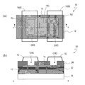
- FIG. 4A and 4B are diagrams illustrating a configuration of a TFT according to Embodiment 2, in which FIG. 5A is a plan view, and FIG. 5B is a cross-sectional view taken along line xx of FIG. FIG.
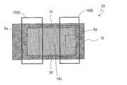
- FIGS. 4A and 4B are diagrams showing a configuration of a TFT according to Embodiment 3, wherein FIG. 5A is a plan view, and FIG. 5B is a cross-sectional view taken along line xx of FIG. It is a top view for demonstrating the magnitude relationship of the width
- FIG. 10 is a plan view illustrating a configuration of a TFT according to a modified example of Embodiment 3. It is a top view which shows the structure of TFT of Embodiment 4, (a) and (b) show another form, respectively.
- TFT substrate active matrix substrate
- the active matrix substrate according to the embodiment of the present invention may be, for example, a vertical electric field mode (for example, VA (Vertical Alignment), TN (Twisted Nematic)) or a horizontal electric field mode (for example, IPS (In Plane Switching), FFS (Fringe Field Switching).
- VA Vertical Alignment
- TN Transmission Nematic
- IPS In Plane Switching
- FFS Ringe Field Switching
- the liquid crystal display device operating in ()) is preferably used. Further, it is also suitably used in other display devices such as an organic EL display device.
- the structure of the TFT formed on the active matrix substrate according to the embodiment of the present invention can also be applied to a power device (for example, a power supply circuit, a high voltage I / O device, etc.) configured using the TFT.
- a power device for example, a power supply circuit, a high voltage I / O device, etc.
- the active matrix substrate according to the embodiment of the present invention is provided with a display area and a frame area outside the display area.
- a plurality of pixels are arranged in a matrix in the display area, and each of the plurality of pixels is provided with a pixel TFT as an active element.
- a monolithic driver is provided in the frame region, a plurality of peripheral circuit TFTs constituting the monolithic driver are provided in the frame region.
- FIG. 1 is a plan view showing a TFT 90 (peripheral circuit TFT) of a comparative example provided in the frame region.
- the TFT 90 may be included in a shift register that forms a monolithic gate driver.
- the TFT 90 may be an output buffer transistor whose drain is connected to a gate wiring.
- the TFT 90 includes a gate electrode 92, a gate insulating layer (not shown) covering the gate electrode 92, and an island-shaped oxide semiconductor layer 94 provided to overlap the gate electrode 92 with the gate insulating layer interposed therebetween. have.
- a source electrode 96 and a drain electrode 98 are connected to the oxide semiconductor layer 94, respectively.
- the source electrode 96 and the drain electrode 98 are spaced apart from each other so that a channel region 94C is formed therebetween.
- the source electrode 96 and the drain electrode 98 are provided as part of the source line 6 and the drain line 8 that extend linearly across the end of the oxide semiconductor layer 94, respectively.
- a connection region between the source line 6 and the oxide semiconductor layer 94 (hereinafter also referred to as a source connection region Rs) is a region corresponding to the source electrode 96 of the TFT 90, and the drain line 8 and the oxide semiconductor.
- a connection region with the layer 94 (hereinafter sometimes referred to as a drain connection region Rd) is a region corresponding to the drain electrode 98 of the TFT 90.
- the channel region 94C of the TFT 90 is provided between the source connection region Rs and the drain connection region Rd, and the channel width is substantially equal to the width of the oxide semiconductor layer 94.
- the width and the channel width of the oxide semiconductor layer are sometimes referred to as a direction (width direction) orthogonal to a direction from the source electrode to the drain electrode (sometimes referred to as a channel current direction).
- the channel length means the dimension of the channel region in a direction parallel to the direction from the source electrode to the drain electrode.
- the width of the source connection region Rs (or source electrode) and the width of the drain connection region (or drain electrode) mean the respective dimensions in the width direction.
- each TFT 90 can be reduced. Therefore, a large number of TFTs 90 can be arranged in a relatively narrow area.
- the TFT 90 having such a configuration has a large overlapping area between the drain electrode 98 and the oxide semiconductor layer 94, when the potential on the drain electrode side is high, the TFT is off (the gate voltage Vg applied to the gate voltage 92). In a state where the voltage is less than the threshold voltage Vth), a leakage current may flow between the source and the drain.
- Peripheral circuit TFTs included in the gate driver include those to which a higher drain voltage is applied at the time of turning off than the pixel TFTs.
- a high voltage is applied to the drain electrode 98 side in the off period of the TFT 90, capacitive coupling is generated between the oxide semiconductor layer 94 and the drain electrode 98, whereby the channel region 94C of the oxide semiconductor layer 94 is activated. This is considered to increase the leakage current.
- the present inventor has determined the width or area of the connection region (source connection region Rs) between the drain electrode and the oxide semiconductor layer in the peripheral circuit TFT as the connection region (drain connection region Rd) between the source electrode and the oxide semiconductor layer. ) was considered to be smaller than the width or area.
- This configuration can be realized, for example, by setting the width of the drain electrode smaller than the width of the source electrode.
- the source connection region Rs and the drain connection region Rd have an asymmetric shape. In this specification, such a structure may be referred to as a source / drain asymmetric structure.
- the drain potential is changed to the channel potential even when a high voltage is applied to the drain side when the TFT is turned off.
- the influence exerted is reduced, and the leakage current can be suppressed.
- leakage current can be suppressed without increasing the channel length, a narrow frame can be realized by designing the TFT size to be relatively small.
- the area of the source connection region is sufficiently secured and the channel length is relatively short, a decrease in on-current can be prevented.
- the above-described source / drain asymmetric structure is selectively applied to a TFT that requires a particularly high breakdown voltage among the peripheral circuit TFTs (that is, a TFT in which a voltage applied to the drain electrode is relatively large when turned off),
- a source / drain symmetrical structure as shown in FIG. 1 may be applied.
- a TFT requiring high breakdown voltage for example, in a shift register constituting a monolithic gate driver, the gate of a TFT (for example, an output buffer transistor) designed to be turned on by bootstrap as described later is used.
- various TFTs whose drains are connected can be mentioned.
- a source / drain asymmetric structure is applied only to such a specific TFT, a TFT having a source / drain asymmetric structure and a TFT having a source / drain symmetrical structure are mixed in a monolithic gate driver.
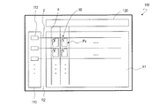
- FIG. 2 is a plan view schematically showing the overall configuration of the active matrix substrate 100 of the first embodiment.
- the active matrix substrate 100 has a display region R1 and a frame region R2 that is a non-display region provided outside the display region R1.
- the frame region R2 is provided as a band-like region located on the upper side and the left side of the display region R1.
- the frame region R2 may be provided in another manner, for example, may be provided only below the display region R1.
- Each pixel Px includes a pixel TFT 50 as a switching element.
- the gate of the pixel TFT 50 is connected to the gate bus line 2 extending along the horizontal direction (row direction), and the source of the pixel TFT 50 is connected to the source bus line 4 extending along the vertical direction (column direction).
- the drain of the pixel TFT 50 is connected to the pixel electrode.
- the gate driver 110 and the source driver 120 are provided on the left and upper strip regions of the display region R1, respectively.
- the gate driver 110 is a monolithic gate driver, and is a circuit that is integrally formed on a substrate using a manufacturing process for manufacturing the pixel TFT 50 and the like.
- the source driver 120 may be provided as a driver monolithically formed on the substrate, similarly to the gate driver 110, or may be provided by mounting an IC chip.
- the gate driver 110 supplies the gate voltage Vg to the gate electrode of the pixel TFT 50 through the gate bus line 2 connected in common to the plurality of pixels Px arranged in the row direction. More specifically, the gate driver 110 includes a plurality of shift registers 112 respectively connected to each of the plurality of gate bus lines 2 extending in parallel with each other in the row direction, and each row driver 110 has a predetermined timing. The gate-on voltage Vgh is sequentially supplied to each pixel Px.
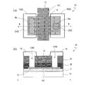
- FIGS. 3A and 3B are a plan view and a cross-sectional view showing a configuration related to some TFTs 5 (peripheral circuit TFTs) among a plurality of TFTs included in the shift register 112 configuring the gate driver 110.
- the TFT 5 may be a specific TFT that requires a particularly high breakdown voltage among a plurality of TFTs constituting the shift register 112.
- the TFT 5 of the present embodiment is formed in an island shape on the insulating substrate 10 so as to overlap with the gate electrode 12, the gate insulating layer 20 covering the gate electrode 12, and the gate electrode 12 via the gate insulating layer 20.
- the oxide semiconductor layer 14 is provided.
- a source electrode 16 and a drain electrode 18 provided so as to be separated from each other are connected to the upper surface of the oxide semiconductor layer 14, and the oxide semiconductor layer 14 is interposed between the source electrode 16 and the drain electrode 18.
- a channel region 14C is formed.
- the source electrode 16 is provided as a part of the source line 6 (source bus line 4 shown in FIG. 2) that extends linearly in the vertical direction across the left end of the oxide semiconductor layer 14.
- the source electrode 16 is a portion corresponding to a connection region (source connection region Rs) between the source line 6 and the oxide semiconductor layer 14.
- the width of the source electrode 16 (or the source connection region Rs) is the same as the width of the oxide semiconductor layer 14.
- the gate electrode 12 exists not only in the oxide semiconductor layer 14 but also under the source line 6.
- the drain electrode 18 is provided with a narrower width so as to fit inside the oxide semiconductor layer 14 in the width direction.
- the drain electrode 18 has a shape protruding from the right to the left in the drawing toward the source electrode 16, and a connection region Rd with the oxide semiconductor layer 14 is formed at the tip.
- a drain line connected to the opposite side of the drain electrode 18 to the source electrode 16 side may be provided in parallel with the source line 6.
- the drain line is provided so as not to cover the oxide semiconductor layer 14, for example, but may slightly overlap the right end portion of the oxide semiconductor layer 14.
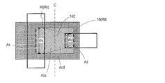
- the width Wd of the drain connection region Rd is smaller than the width Ws of the source connection region Rs.
- the area Ad of the drain connection region Rd is smaller than the area As of the source connection region Rs.
- the width Wd of the drain connection region Rd is set to, for example, 0.5 to 0.8 times the width Ws of the source connection region Rs.
- the Further, the area Ad of the drain connection region Rd is set to, for example, 0.5 to 0.8 times the area As of the source connection region Rs.
- the effective channel region 14C formed between the source connection region Rs and the drain connection region Rd has a trapezoidal shape with the edge of the source electrode 16 as the bottom and the edge of the drain electrode 18 as the bottom. Is formed.
- this channel region 14C is divided by a straight line C passing through the center of the source / drain in the channel current direction and orthogonal to the channel current direction, the channel region 14C is closer to the drain electrode 18 than the effective channel region area Acs on the source electrode 16 side.
- the effective area Acd of the channel region is smaller.
- the effective channel region 14C is described as a trapezoidal region surrounded by an edge of the source connection region Rs, an edge of the drain connection region Rd, and two straight lines connecting these ends for convenience.
- the outer portion of the oxide semiconductor layer 14 near the trapezoidal region can also function as the channel of the TFT 5.
- FIG. 5 shows a case where an oxide semiconductor TFT employs a source / drain asymmetric structure (S / D asymmetry: FIG. 3) and a case where a source / drain symmetrical structure (S / D symmetry: FIG. 1) is employed.
- the leakage current is suppressed when the S / D asymmetry is made.
- FIG. 2 A configuration example of the gate driver 110 shown in FIG. 2 will be described with reference to FIGS. 6 and 7.
- a configuration similar to that of the gate driver 110 shown in FIGS. 6 and 7 is described in International Publication No. 2011/024499 (Patent Document 2).
- Patent Document 2 the entire disclosure of WO 2011/024499 is incorporated herein by reference.
- FIG. 6 is a diagram illustrating a circuit configuration example of the gate driver 110.
- the gate driver 110 includes a plurality of stages of shift registers 112.
- the shift register 112 at each stage corresponds to each row of the pixel matrix.
- the shift register 112 includes 2a bistable circuits, and each bistable circuit is configured to switch and output one of the two stable states by a trigger signal.
- Each of the bistable circuits has an input terminal for receiving a four-phase clock signal CKA, CKB, CKC, CKD, an input terminal for receiving a set signal S, an input terminal for receiving a reset signal R, and an input for receiving a clear signal CLR.
- a terminal, an input terminal for receiving a low potential DC voltage VSS, and an output terminal for outputting a status signal Q are provided.
- the outer periphery of the frame region has a main wiring for gate clock signals (first gate clock signal CK1, second gate clock signal CK1B, third gate clock signal CK2, and fourth gate clock signal CK2B), low A trunk wiring for the direct current voltage VSS and a trunk wiring for the clear signal CLR are provided.
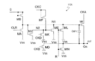
- FIG. 7 is a circuit diagram showing a more detailed configuration of the bistable circuit 112A (configuration of one stage of the shift register 112).
- the bistable circuit 112A includes ten thin film transistors (MA, MB, MI, MF, MJ, MK, ME, ML, MN, and MD) and a capacitor CAP1.
- the bistable circuit 112A includes an input terminal that receives the clock signals CKA, CKB, CKC, and CKD, an input terminal that receives the set signal S, an input terminal that receives the reset signal R, an input terminal that receives the clear signal CLR, and a state An output terminal OUT for outputting the signal Qn is provided.
- the source terminal of the thin film transistor MB, the drain terminal of the thin film transistor MA, the gate terminal of the thin film transistor MJ, the drain terminal of the thin film transistor ME, the drain terminal of the thin film transistor ML, the gate terminal of the thin film transistor MI, and one end of the capacitor CAP1 are connected to each other.
- the wiring part in which these are connected to each other is referred to as a “first node” for the sake of convenience, and is denoted by reference numeral N1 in the drawing.
- the drain terminal of the thin film transistor MJ, the drain terminal of the thin film transistor MK, the source terminal of the thin film transistor MF, and the gate terminal of the thin film transistor ME are connected to each other.
- the wiring part in which these are connected to each other is referred to as a “second node” for the sake of convenience, and is indicated by a symbol N2 in the drawing.
- the thin film transistor MA shown on the left side of the drawing sets the potential of the first node N1 to the low level when the clear signal CLR is at the high level.
- the thin film transistor MB sets the potential of the first node N1 to a high level when the set signal S is at a high level.
- the thin film transistor MI shown on the right side of the figure functions as an output buffer transistor, and applies the potential of the first clock signal CKA to the output terminal when the potential of the first node N1 is at a high level.
- the thin film transistor MF shown in the upper center of the figure sets the potential of the second node N2 to a high level when the third clock signal CKC is at a high level.
- the thin film transistor MJ makes the potential of the second node N2 low level when the potential of the first node N1 is high level. If the second node N2 becomes high level and the thin film transistor ME is turned on during the period when the gate bus line connected to the output terminal OUT of the bistable circuit 112A is selected, the potential of the first node N1 becomes As a result, the thin film transistor MI is turned off. In order to prevent such a phenomenon, a thin film transistor MJ is provided.
- the thin film transistor MK makes the potential of the second node N2 low level when the fourth clock signal CKD is high level. If the thin film transistor MK is not provided, the potential of the second node N2 is always at a high level during a period other than the selection period, and a bias voltage is continuously applied to the thin film transistor ME. Then, the threshold voltage of the thin film transistor ME increases, and the thin film transistor ME does not function sufficiently as a switch. In order to prevent such a phenomenon, a thin film transistor MK is provided.
- the thin film transistor ME sets the potential of the first node N1 to low level when the potential of the second node N2 is high level.
- the thin film transistor ML sets the potential of the first node N1 to low level when the reset signal R is at high level.
- the thin film transistor MN makes the potential of the output terminal low level when the reset signal R is high level.
- the thin film transistor MD sets the potential of the output terminal OUT to a low level when the second clock CKB is at a high level.
- the capacitor CAP1 functions as a compensation capacitor for maintaining the potential of the first node N1 at a high level during the period when the gate bus line connected to the output terminal OUT of the bistable circuit 112A is selected.
- the first node N1 shown in FIG. 7 is a node whose potential is boosted above the power supply voltage by bootstrap.
- the bootstrap means that when the output buffer transistor MI is turned on, the voltage applied to the gate terminal via the parasitic capacitance due to the rise of the source potential of the output buffer transistor MI and the storage of the capacitor CAP1. This means an operation of turning on the output buffer transistor MI in a state where the gate voltage is raised to a potential exceeding the set signal S.
- the drain sides of the thin film transistors MA, ME, and ML that pull down the first node N1 are connected to the first node N1, and the source side is connected to VSS.
- the first node N1 becomes a high voltage
- the thin film transistors MA, ME, ML are in an off state, and a high voltage is applied between the drain and the source.
- the channel lengths of the thin film transistors MA, ME, and ML are short and the off breakdown voltage is low, the normal off state cannot be maintained.
- the first node N1 potential is lowered and the driver selection / non-selection operation is broken. There is a risk.
- the clock signal CKA having a duty ratio of 50% is input to the drain terminal of the output buffer transistor MI. However, if this stage is not selected, the clock signal CKA should not be output as the status signal Qn. When the off-breakdown voltage of the transistor MI is low, the voltage of the clock signal CKA is output as the status signal Qn even when it is not selected, causing malfunction.
- the thin film transistor as described above is required to have a high breakdown voltage.
- the off breakdown voltage of the thin film transistor tends to increase, and it becomes easy to ensure the operation of the driver.
- the layout area of the gate driver increases. This leads to an increase in the outer dimensions of the display panel, which makes it impossible to meet the demand for device miniaturization.
- the configuration (source / drain asymmetric structure) of the TFT 5 of the present embodiment described with reference to FIGS. 3 and 4 is applied to the thin film transistor that is required to have an off breakdown voltage.
- the off breakdown voltage can be improved without increasing the size of the device.
- the structure of the TFT 90 of the comparative example shown in FIG. 1 may be applied to the thin film transistors MD, MF, MN, and the like that do not particularly require off-voltage resistance.
- the above source / drain asymmetric structure may be applied to any TFT in which a high voltage may be applied to the drain side when the monolithic gate driver is off.
- a source / drain asymmetric structure to a TFT in which the voltage applied to the drain side when off can be 20 to 60V.
- the peripheral circuit TFT5 can be manufactured by using a manufacturing process applied to the pixel TFT 50 (see FIG. 2) provided in the display region R1.
- the gate electrode 12 is formed on the substrate 10. More specifically, a metal film (Mo, Ti, Al, Ta, Cr, Au, etc.) to be a gate electrode is formed on a glass substrate with a thickness of 100 to 300 nm by a sputtering apparatus. This metal film may have a laminated structure (for example, Ti / Al / Ti). After the film formation, the gate electrode 12 and the like can be obtained by patterning the metal film by photolithography.
- a metal film Mo, Ti, Al, Ta, Cr, Au, etc.
- the gate insulating layer 20 is formed. More specifically, the gate insulating layer 20 is obtained by forming the silicon oxide film SiO 2 or the silicon nitride film SiN x with a plasma CVD apparatus at a temperature of 300 to 400 ° C. to a thickness of 300 to 400 nm.
- the gate insulating layer 20 may have a laminated structure of SiO 2 and SiN x .
- the oxide semiconductor layer 14 as an active layer is formed. More specifically, a thin film made of an oxide semiconductor (such as an In—Ga—Zn—O based semiconductor, an In—Zn—O based semiconductor, or a ZnO based semiconductor) is formed at a temperature of 200 to 400 ° C. with a sputtering apparatus at a temperature of 40 to 40 ° C. It is formed with a thickness of 50 nm. Thereafter, an inert argon gas Ar (flow rate: 100 to 300 sccm) and oxygen gas O 2 (flow rate: 5 to 20 sccm) may be introduced into the sputtering apparatus.
- an inert argon gas Ar flow rate: 100 to 300 sccm
- oxygen gas O 2 flow rate: 5 to 20 sccm
- the oxide semiconductor film may be formed with a thickness of 40 to 50 nm by a coating process instead of a sputtering method. After the film formation, the oxide semiconductor film is patterned by a photolithography method, whereby the island-shaped oxide semiconductor layer 14 that becomes the active layer of each TFT can be obtained.
- the dimension in the width direction of the oxide semiconductor layer 14 is set to 5 ⁇ m to 50 ⁇ m, for example, and the dimension in the channel current direction is set to 10 ⁇ m to 20 ⁇ m, for example.
- source / drain electrodes 16 and 18 are formed. More specifically, a source / drain electrode is formed by forming a metal film (Mo, Ti, Al, Ta, Cr, Au, etc.) with a thickness of 100 to 300 nm by a sputtering apparatus and patterning it with a photolithography method. 16, 18 are obtained. In this step, the TFT 5 is completed.
- the metal film may have a laminated structure (for example, Ti / Al / Ti).
- the shape and arrangement of the source / drain electrodes 16, 18 are set so that the width and area of the drain connection region Rd are smaller than the width and area of the source connection region Rs. Select as appropriate.
- a mask pattern or alignment for determining a resist pattern may be appropriately selected.
- the width of the source connection region Rs (equivalent to the width of the oxide semiconductor layer 14 in this embodiment) may be, for example, 5 ⁇ m to 50 ⁇ m, and the width of the drain connection region Rd may be, for example, 2.5 ⁇ m to It may be 40 ⁇ m. Further, the distance between the source and the drain (that is, the channel length of the TFT 5) may be, for example, 5 ⁇ m to 15 ⁇ m.
- a passivation layer (not shown) as a protective layer covering the TFT 5 is formed as necessary. More specifically, the oxide film SiO 2 or the nitride film SiN x is formed with a plasma CVD apparatus at a temperature of 200 to 300 ° C. to a thickness of 200 to 300 nm.
- the protective layer may have a laminated structure of SiO 2 and SiN x .
- heat treatment is performed at a temperature of 200 to 400 ° C. for 1 to 2 hours in dry air or air.
- the element characteristics of the TFT 5 can be improved by this heat treatment.
- the process for manufacturing the TFT 5 described above is common to the process of manufacturing the pixel TFT 50, and each corresponding component of the pixel TFT 50 can be formed by each of the above processes.
- a step of forming an organic interlayer insulating film, a step of forming a transparent common electrode, and further through an insulating layer A step of forming a pixel electrode or the like may be performed. Since these steps can be performed by a known method, description thereof is omitted here.
- the oxide semiconductor layer 14 includes, for example, an In—Ga—Zn—O-based semiconductor (hereinafter abbreviated as “In—Ga—Zn—O-based semiconductor”).
- a TFT having an In—Ga—Zn—O-based semiconductor layer has high mobility (more than 20 times that of an a-Si TFT) and low leakage current (less than one hundredth of that of an a-Si TFT). It is suitably used as a drive TFT and a pixel TFT.
- a TFT having an In—Ga—Zn—O-based semiconductor layer is used, power consumption of the display device can be significantly reduced.
- the In—Ga—Zn—O based semiconductor may be amorphous or may contain a crystalline part.
- a crystalline In—Ga—Zn—O-based semiconductor in which the c-axis is oriented substantially perpendicular to the layer surface is preferable.
- Such a crystal structure of an In—Ga—Zn—O-based semiconductor is disclosed in, for example, Japanese Patent Application Laid-Open No. 2012-134475 (Patent Document 1). For reference, the entire disclosure of Japanese Patent Application Laid-Open No. 2012-134475 is incorporated herein by reference.
- the oxide semiconductor layer 14 may include another oxide semiconductor instead of the In—Ga—Zn—O-based semiconductor.
- Zn—O based semiconductor ZnO
- In—Zn—O based semiconductor IZO (registered trademark)
- Zn—Ti—O based semiconductor ZTO
- Cd—Ge—O based semiconductor Cd—Pb—O based
- CdO cadmium oxide
- Mg—Zn—O based semiconductors In—Sn—Zn—O based semiconductors (eg, In 2 O 3 —SnO 2 —ZnO), In—Ga—Sn—O based semiconductors, etc. You may go out.
- a counter substrate is prepared separately from the active matrix substrate 100, and a liquid crystal layer is provided between the active matrix substrate 100 and the counter substrate. What is necessary is just to employ
- the counter substrate can be obtained by providing a counter electrode formed of a transparent conductive film (for example, an ITO film having a thickness of 100 nm) on a glass substrate.
- a transparent conductive film for example, an ITO film having a thickness of 100 nm
- RGB color filters may be provided on the counter substrate.
- a photo spacer for maintaining a gap between the counter substrate and the active matrix substrate 100 may be provided on the counter substrate. Note that the color filter and the photo spacer may be provided on the active matrix substrate 100.
- a liquid crystal panel for example, the active matrix substrate 100 and the counter substrate are bonded together with a gap between them using an annular sealing material disposed on the outer periphery, and then surrounded by the sealing material. A liquid crystal material may be injected into the gap between the substrates.
- a liquid crystal panel may be manufactured by providing a sealant or a photo spacer on the counter substrate, dropping a liquid crystal material, and then bonding the active matrix substrate 100 and the counter substrate.
- segmenting into each liquid crystal panel is performed.
- a backlight unit is provided on the back surface (TFT substrate side) of the liquid crystal panel.
- the backlight unit may be provided with various optical elements such as a diffusion film.
- the source / drain asymmetric structure described above may be applied to the peripheral circuit TFT 5, and the source / drain asymmetric structure may also be applied to the pixel TFT 50.
- Embodiment 2 Hereinafter, the active matrix substrate of Embodiment 2 will be described.
- the main difference between the active matrix substrate of the second embodiment and the active matrix substrate 100 of the first embodiment is that the oxide semiconductor layer 14 in at least a part of the TFTs 52 (peripheral circuit TFTs) constituting the monolithic gate driver.
- the top gate type TFT structure in which the gate electrode 12 is disposed on the upper layer is employed.
- the same reference numerals are assigned to components common to the active matrix substrate 100 of Embodiment 1 to avoid duplication of description.
- FIGS. 8A and 8B are plan views showing configurations related to some TFTs 52 (peripheral circuit TFTs) among a plurality of TFTs included in the shift register constituting the monolithic gate driver in the active matrix substrate of this embodiment. It is a figure and sectional drawing.
- the TFT 52 may be a specific TFT that requires a particularly high breakdown voltage among a plurality of TFTs constituting the shift register.
- the TFT 52 includes a buffer layer 11 (for example, a SiO 2 film or a SiN x film having a thickness of 100 to 300 nm), an island-shaped oxide semiconductor layer 14, and gate insulation covering the oxide semiconductor layer 14 on the insulating substrate 10.
- the gate electrode 12 is provided so as to overlap with the oxide semiconductor layer 14 with the layer 20 interposed therebetween.
- an interlayer insulating layer 22 (for example, a SiO 2 film or a SiN x film having a thickness of 200 to 300 nm) is provided so as to cover the gate electrode 12.
- drain electrode 16 and the source electrode 18 are provided on the interlayer insulating layer 22.
- the drain electrode 16 and the source electrode 18 are connected to the upper surface of the oxide semiconductor layer 14 through the source contact hole CHS and the drain contact hole CHD provided so as to penetrate the gate insulating layer 20 and the interlayer insulating layer 22, respectively. Yes.
- a connection region (source connection region Rs) between the source electrode 16 and the oxide semiconductor layer 14 is formed in the source contact hole CHS, and the drain electrode 18 and the oxide semiconductor layer 14 are formed in the drain contact hole CHD.
- a connection region (drain connection region Rd) is formed.
- the source electrode 16 and the drain electrode 18 may be a part of the source line 6 and the drain line 8 that extend along the width direction.
- the source connection region Rs and the drain connection region Rd are formed so as to be separated from each other at both ends of the oxide semiconductor layer 14, and the channel of the oxide semiconductor layer 14 is provided between the source connection region Rs and the drain connection region Rd. Region 14C is formed.
- FIG. 9 is a diagram for explaining the magnitude relationship among the width Ws of the source connection region Rs, the width Wd of the drain connection region Rd, the area As of the source connection region Rs, the area Ad of the drain connection region Rd, and the like.
- the width Wd of the drain connection region Rd is smaller than the width Ws of the source connection region Rs.
- the area Ad of the drain connection region Rd is smaller than the area As of the source connection region Rs.
- the effective channel region on the drain electrode 18 side is larger than the effective area Acs on the source electrode 16 side.
- the area Acd is smaller.
- the width Wd of the drain connection region Rd is, for example, 0.5 times the width Ws of the source connection region Rs in order to effectively suppress the off-leakage current while preventing a decrease in the on-current. More than 0.8 times is set.
- the width of the oxide semiconductor layer 14 and the width Ws of the source connection region Rs may be different.
- the shape of the source contact hole CHS is determined such that the width Ws of the source connection region Rs is smaller than the width of the oxide semiconductor layer 14.
- the width of the source contact hole CHS may be larger than the width of the oxide semiconductor layer 14, and in this case, the width Ws of the source connection region Rs is equivalent to the width of the oxide semiconductor layer 14.
- the TFT 52 of this embodiment also uses a source / drain symmetric structure (S / D symmetry) when a source / drain asymmetric structure (S / D asymmetric) is used, as in the graph shown in FIG. It has been confirmed that the off-leakage current is reduced as compared with the case of the above.
- the buffer layer 11 is formed on the insulating substrate 10.
- the buffer layer 11 is obtained, for example, by forming a SiO 2 film or a SiN x film having a thickness of 100 to 300 nm at a temperature of 200 to 300 ° C. with a plasma CVD apparatus.
- the oxide semiconductor layer 14 is formed by a process similar to that of the TFT 5 of the first embodiment. Further, the gate insulating layer 20 is formed over the oxide semiconductor layer 14 by a process similar to that of the TFT 5. Further, the gate electrode 12 is formed so as to overlap the oxide semiconductor layer 14 with the gate insulating layer 20 interposed therebetween by the same process as the TFT 5.
- an interlayer insulating layer 22 is formed. More specifically, the interlayer insulating layer 22 is obtained by forming a SiO 2 film or a SiN x film with a thickness of 200 to 300 nm at a temperature of 200 to 300 ° C. using a plasma CVD apparatus.
- the interlayer insulating layer 22 may have a laminated structure of a SiO 2 film and a SiN x film.
- a pair of contact holes CHS and CHD penetrating through the interlayer insulating layer 22 and the gate insulating layer 20 are formed by performing a photolithography process and dry or wet etching. At this time, the contact holes CHS and CHD are formed so that the area and width of the drain contact hole CHD are smaller than the area and width of the source contact hole CHS.
- the source electrode 16 and the drain electrode 18 are formed by the same process as the TFT 5.
- the source electrode 16 and the drain electrode 18 may be formed as part of the source line 6 and the drain line 8.
- the source electrode 16 and the drain electrode 18 are provided so as to completely cover the source contact hole CHS and the drain contact hole CHD, respectively.
- the source electrode 16 is connected to the oxide semiconductor layer 14 inside the source contact hole CHS to form the source connection region Rs
- the drain electrode 18 is connected to the oxide semiconductor layer 14 inside the drain contact hole CHD.
- the drain connection region Rs is formed.
- the width and area of the source connection region Rs are determined by the size of the source contact hole CHS, and the width and area of the drain connection region Rd are determined by the size of the drain contact hole CHD. Since the size of each contact hole is set as described above, the width and area of the drain connection region Rd are smaller than the width and area of the source connection region Rs.
- the same heat treatment as that of the TFT 5 may be performed, whereby the element characteristics of the TFT 52 can be improved.
- the process for manufacturing the TFT 52 described above is common to the process for manufacturing the pixel TFT formed in the display region, and the corresponding constituent elements of the pixel TFT can be formed by the above-described processes. it can.
- the pixel TFT is manufactured to have a top gate type TFT structure.
- Embodiment 3 the active matrix substrate of Embodiment 3 will be described.
- the main difference of the active matrix substrate of the third embodiment from the active matrix substrate 100 of the first embodiment is that at least a part of the TFTs 53 (peripheral circuit TFTs) constituting the monolithic gate driver have an oxide semiconductor layer 14.
- the etch stop layer 24 is provided on the upper layer.
- the same reference numerals are assigned to components common to the TFT substrate 100 to avoid duplication of description.
- FIGS. 10A and 10B are planes showing a configuration related to some TFTs 53 (peripheral circuit TFTs) among a plurality of TFTs included in the shift register constituting the monolithic gate driver in the active matrix substrate of the present embodiment. It is a figure and sectional drawing.
- the TFT 53 may be a specific TFT that requires a particularly high breakdown voltage among a plurality of TFTs constituting the shift register.
- the TFT 53 is an island-shaped oxide semiconductor provided on the insulating substrate 10 so as to overlap the gate electrode 12, the gate insulating layer 20 covering the gate electrode 12, and the gate electrode 12 with the gate insulating layer 20 interposed therebetween.
- Layer 14 is an island-shaped oxide semiconductor provided on the insulating substrate 10 so as to overlap the gate electrode 12, the gate insulating layer 20 covering the gate electrode 12, and the gate electrode 12 with the gate insulating layer 20 interposed therebetween.
- An etch stop layer 24 made of SiO 2 or the like is provided on the oxide semiconductor layer 14.
- the etch stop layer 24 is provided in order to prevent etching damage to the channel region 14C of the oxide semiconductor layer 14 when the metal film is patterned in a source / drain formation process described later.
- the etch stop layer 24 is provided so as to cover the oxide semiconductor layer 14 as a whole.
- the source contact hole CHS is formed at a position corresponding to the left end portion of the oxide semiconductor layer 14 so as to penetrate the etch stop layer 24, and the drain contact hole CHD is formed at a position corresponding to the right end portion. ing.
- the width and area of the source contact hole CHS are formed larger than the width and area of the drain contact hole CHD.
- the source electrode 16 and the drain electrode 18 provided so as to be separated from each other through the source contact hole CHS and the drain contact hole CHD are connected to the oxide semiconductor layer 14.
- a connection region (source connection region Rs) between the source electrode 16 and the oxide semiconductor layer 14 is formed in the source contact hole CHS, and the drain electrode 18 and the oxide semiconductor layer 14 are formed in the drain contact hole CHD.
- Connection region (drain connection region Rd) is formed.
- the source electrode 16 and the drain electrode 18 may be part of the source line 6 and the drain line 8 that extend along the vertical direction.
- the source connection region Rs and the drain connection region Rd are formed so as to be separated from each other at both ends of the oxide semiconductor layer 14, and the channel of the oxide semiconductor layer 14 is provided between the source connection region Rs and the drain connection region Rd. Region 14C is formed.
- FIG. 11 is a diagram for explaining the relationship among the width Ws of the source connection region Rs, the width Wd of the drain connection region Rd, the area As of the source connection region Rs, the area Ad of the drain connection region Rd, and the like in the TFT 53.
- the width Wd of the drain connection region Rd is smaller than the width Ws of the source connection region Rs.
- the area Ad of the drain connection region Rd is smaller than the area As of the source connection region Rs.
- the effective channel region on the drain electrode 18 side is larger than the effective channel region area Acs on the source electrode 16 side.
- the area Acd is smaller.
- the TFT 53 having the etch stop layer 24 adopts the source / drain asymmetric structure
- the off-leak current can be suppressed when a high voltage is applied to the drain side.
- the TFT 53 of this embodiment also uses a source / drain symmetric structure (S / D symmetry) when a source / drain asymmetric structure (S / D asymmetric) is used, as in the graph shown in FIG. It has been confirmed that the off-leakage current is reduced as compared with the case of the above.
- the gate electrode 12, the gate insulating layer 20, and the oxide semiconductor layer 14 are formed on the insulating substrate 10 by a process similar to that of the TFT 5 of Embodiment 1.
- the etch stop layer 24 is formed so as to cover at least a portion to be a channel region of the oxide semiconductor layer 14. More specifically, the SiO 2 film was formed to a thickness of a temperature at 100 ⁇ 400 nm of 300 ⁇ 400 ° C. using a plasma CVD device, a pair of contact holes CHS in the SiO 2 film by photolithography, By providing CHD, the etch stop layer 24 can be obtained. At this time, the contact holes CHS and CHD are formed so that the area and width of the drain contact hole CHD are smaller than the area and width of the source contact hole CHS.
- the source electrode 16 and the drain electrode 18 are formed by the same process as the TFT 5.
- the source electrode 16 and the drain electrode 18 are provided as part of the source line 6 and the drain line 8 so as to completely cover the source contact hole CHS and the drain contact hole CHD, respectively.
- the source electrode 16 is connected to the oxide semiconductor layer 14 inside the source contact hole CHS to form the source connection region Rs
- the drain electrode 18 is connected to the oxide semiconductor layer 14 inside the drain contact hole CHD.
- the drain connection region Rs is formed.
- the width and area of the source connection region Rs are determined by the size of the source contact hole CHS, and the width and area of the drain connection region Rd are determined by the size of the drain contact hole CHD. Since the size of each contact hole is set as described above, the width and area of the drain connection region Rd are smaller than the width and area of the source connection region Rs.
- a protective layer (not shown) may be provided similarly to the TFT 5 of the first embodiment.
- an oxide film SiO 2 or a nitride film SiN x is formed with a plasma CVD apparatus at a temperature of 200 to 300 ° C. to a thickness of 200 to 300 nm.
- the protective film may have a laminated structure of SiO 2 and SiN x . Further, the same heat treatment as that of the TFT 5 of Embodiment 1 may be performed, whereby the element characteristics of the TFT 53 can be improved.
- the process for manufacturing the TFT 53 described above is common to the process for manufacturing the pixel TFT formed in the display region, and the corresponding constituent elements of the pixel TFT can be formed by the above-described processes. it can.
- the pixel TFT is provided with the etch stop layer 24 together with the peripheral circuit TFT 53, and etching damage to the channel region in the oxide semiconductor layer is reduced.
- an etch stop layer 24 ′ is provided in an island shape so as to cover at least the channel portion 14C of the oxide semiconductor layer 14. It has been. However, the island-like etch stop layer 24 ′ has different asymmetric shapes on the source side and the drain side.
- the island-shaped etch stop layer 24 ′ covers the channel region 14C of the oxide semiconductor layer 14, but is provided so as to expose the end of the oxide semiconductor layer 14. It has been.
- the source electrode 16 and the drain electrode 18 are formed so as to cover the respective lateral edges of the etch stop layer 24 ′, and the connection regions Rs and Rd are formed in the exposed portion of the oxide semiconductor layer 14.
- the etch stop layer 24 has different edge shapes on the source side and the drain side. More specifically, the source side has a straight edge that crosses the oxide semiconductor layer, whereas the drain side has a rectangular notch that partially exposes the oxide semiconductor layer at the edge. Is formed. By connecting the drain electrode 18 to the oxide semiconductor layer 14 exposed at the notch, a drain connection region having a smaller width and area than the source side can be obtained.
- Embodiment 4 the active matrix substrate of Embodiment 4 will be described.
- the main difference of the active matrix substrate of the fourth embodiment from the active matrix substrate 100 of the first embodiment is that at least some of the TFTs 54a and 54b (peripheral circuit TFTs) constituting the monolithic gate driver are different from the source side.
- An oxide semiconductor layer 14 ′ having a plane shape asymmetric with respect to the drain side is used.
- the same reference numerals are assigned to components common to the TFT substrate 100 to avoid duplication of description.
- FIG. 13A is a plan view showing a configuration related to the peripheral circuit TFT 54a in the active matrix substrate of the present embodiment.
- the TFT 54a may be a specific TFT that requires a particularly high breakdown voltage among a plurality of TFTs included in the monolithic gate driver.
- the TFT 54a is a bottom gate type TFT, and has a gate electrode 12, a gate insulating layer, and an oxide semiconductor layer 14 'on an insulating substrate, like the TFT 5 of the first embodiment.
- the oxide semiconductor layer 14 ′ has a trapezoidal planar shape having an upper base and a lower base substantially parallel to the channel width direction.
- the source line 6 extends linearly in parallel with the channel width direction so as to cover the bottom of the oxide semiconductor layer 14 '.
- a portion of the source line 6 connected to the oxide semiconductor layer 14 ′ functions as the source electrode 16, and a source connection region Rs is formed in this portion.
- drain line 8 extends linearly in parallel with the channel width direction so as to cover the upper bottom of the oxide semiconductor layer 14 ′.
- a portion of the drain line 8 connected to the oxide semiconductor layer 14 ′ functions as the drain electrode 18, and a drain connection region Rd is formed in this portion.
- the planar shape of the oxide semiconductor layer 14 ′ is provided in an asymmetric trapezoid between the source side and the drain side, whereby the width and area of the drain connection region Rd are made smaller than the width and area of the source connection region Rs. Can do.
- FIG. 13B is a plan view showing a configuration related to the peripheral circuit TFT 54b according to a modification of the present embodiment.
- the oxide semiconductor layer 14 ′ has a horizontal T-shaped (convex) planar shape, and the T-shaped upper side portion extending in the channel width direction is the source. Connected to the line 6, the T-shaped protruding portion is connected to the drain line 8. Even in such a configuration, the width and area of the drain connection region Rd can be made smaller than the width and area of the source connection region Rs.
- the source line 6 and the drain line 8 can be disposed relatively close to each other by making the shape of the oxide semiconductor layer 14 ′ asymmetrical between the source side and the drain side.
- the oxide semiconductor layer 14 is connected to the source electrode 16 and the drain electrode 18 through a pair of contact holes having different areas provided in the interposed insulating layer (Embodiments 2 and 3), A part of the source line 6 and the drain line 8 extending in a straight line can be used as the source electrode 16 and the drain electrode 18. Therefore, the process of providing an insulating layer between the oxide semiconductor layer 14 ′ and the source / drain electrodes 16 and 18 can be omitted, and the element size can be set smaller.
- the configuration in which the oxide semiconductor layer 14 ′ has a source / drain asymmetric shape as in the fourth embodiment can be applied in combination with the TFT described in the first to third embodiments.
- the active matrix substrate according to the embodiment of the present invention is suitably used in a display device such as a liquid crystal display device. Further, in various devices configured using oxide semiconductor TFTs, it can be used to suppress the off-leak current of TFTs that are required to have a high breakdown voltage.
- Gate bus line 4 Source bus line 5 TFT (peripheral circuit TFT) 6 Source Line 8 Drain Line 10 Substrate 11 Buffer Layer 12 Gate Electrode 14 Oxide Semiconductor Layer 16 Source Electrode 18 Drain Electrode 20 Gate Insulating Layer 22 Interlayer Insulating Layer 24 Etch Stop Layer 100 Active Matrix Substrate 110 Gate Driver 112 Shift Register 112A Bistable Circuit 120 Source driver CHS Source contact hole CHD Drain contact hole R1 Display area R2 Frame area Rs Source connection area Rd Drain connection area
Landscapes
- Physics & Mathematics (AREA)
- Nonlinear Science (AREA)
- General Physics & Mathematics (AREA)
- Chemical & Material Sciences (AREA)
- Crystallography & Structural Chemistry (AREA)
- Engineering & Computer Science (AREA)
- Mathematical Physics (AREA)
- Optics & Photonics (AREA)
- Microelectronics & Electronic Packaging (AREA)
- Geometry (AREA)
- Computer Hardware Design (AREA)
- Theoretical Computer Science (AREA)
- Thin Film Transistor (AREA)
- Liquid Crystal (AREA)
Abstract
Description
図2は、実施形態1のアクティブマトリクス基板100の全体構成を模式的に示す平面図である。アクティブマトリクス基板100は、表示領域R1と、表示領域R1の外側に設けられた非表示領域である額縁領域R2とを有している。図2に示す態様において、額縁領域R2は、表示領域R1の上側および左側に位置する帯状の領域として設けられている。ただし額縁領域R2は他の態様で設けられていても良く、例えば、表示領域R1の下側のみに設けられていてもよい。
以下、実施形態2のアクティブマトリクス基板を説明する。本実施形態2のアクティブマトリクス基板が、実施形態1のアクティブマトリクス基板100と異なっている主な点は、モノリシックゲートドライバを構成する少なくとも一部のTFT52(周辺回路TFT)において、酸化物半導体層14の上層にゲート電極12が配置されたトップゲート型のTFT構造が採用されている点である。なお、以下では、実施形態1のアクティブマトリクス基板100と共通する構成要素には同じ参照符号を付し、説明の重複を避ける。
以下、実施形態3のアクティブマトリクス基板を説明する。本実施形態3のアクティブマトリクス基板が、実施形態1のアクティブマトリクス基板100と異なっている主な点は、モノリシックゲートドライバを構成する少なくとも一部のTFT53(周辺回路TFT)において、酸化物半導体層14の上層にエッチストップ層24が設けられている点である。なお、以下では、TFT基板100と共通する構成要素には同じ参照符号を付し、説明の重複を避ける。
以下、実施形態4のアクティブマトリクス基板を説明する。本実施形態4のアクティブマトリクス基板が、実施形態1のアクティブマトリクス基板100と異なっている主な点は、モノリシックゲートドライバを構成する少なくとも一部のTFT54a、54b(周辺回路TFT)において、ソース側とドレイン側とで非対称な平面形状を有する酸化物半導体層14’を用いる点である。なお、以下では、TFT基板100と共通する構成要素には同じ参照符号を付し、説明の重複を避ける。
4 ソースバスライン
5 TFT(周辺回路TFT)
6 ソースライン
8 ドレインライン
10 基板
11 バッファ層
12 ゲート電極
14 酸化物半導体層
16 ソース電極
18 ドレイン電極
20 ゲート絶縁層
22 層間絶縁層
24 エッチストップ層
100 アクティブマトリクス基板
110 ゲートドライバ
112 シフトレジスタ
112A 双安定回路
120 ソースドライバ
CHS ソースコンタクトホール
CHD ドレインコンタクトホール
R1 表示領域
R2 額縁領域
Rs ソース接続領域
Rd ドレイン接続領域
Claims (11)
- 複数の画素が設けられた表示領域と、前記表示領域の外側に設けられた額縁領域とを有し、前記額縁領域において駆動回路を構成する複数の周辺回路TFTを備えたアクティブマトリクス基板であって、
前記複数の周辺回路TFTのそれぞれは、ゲート電極と、前記ゲート電極と絶縁された状態で前記ゲート電極と少なくとも部分的に重なるように配置された酸化物半導体層と、前記酸化物半導体層に接続されたソース電極およびドレイン電極とを有しており、
前記複数の周辺回路TFTのうちの少なくとも一部の周辺回路TFTにおいて、前記酸化物半導体層と前記ソース電極との接続領域であるソース接続領域と、前記酸化物半導体層と前記ドレイン電極との接続領域であるドレイン接続領域とが非対称に形成されている、アクティブマトリクス基板。 - 前記ドレイン接続領域の幅は、前記ソース接続領域の幅よりも小さい、請求項1に記載のアクティブマトリクス基板。
- 前記ドレイン接続領域の面積は、前記ソース接続領域の面積よりも小さい、請求項1または2に記載のアクティブマトリクス基板。
- 前記ドレイン電極の幅は、前記ソース電極の幅よりも小さい、請求項1から3のいずれかに記載のアクティブマトリクス基板。
- 前記酸化物半導体層と前記ソース電極および前記ドレイン電極との間に介在される絶縁層であって、前記ソース電極および前記ドレイン電極に対応する位置にソースコンタクトホールおよびドレインコンタクトホールが形成された絶縁層をさらに有し、
前記ソース電極および前記ドレイン電極は、それぞれ、前記ソースコンタクトホールおよび前記ドレインコンタクトホールの内部で前記酸化物半導体層に接続されており、
前記ソースコンタクトホールと前記ドレインコンタクトホールとが異なる形状を有する、請求項1から3のいずれかに記載のアクティブマトリクス基板。 - 前記絶縁層の上に前記ゲート電極が設けられている、請求項5に記載のアクティブマトリクス基板。
- 前記絶縁層の下に前記ゲート電極が設けられている、請求項5に記載のアクティブマトリクス基板。
- 前記複数の周辺回路TFTは、前記ソース接続領域と前記ドレイン接続領域とが前記非対称に形成されている周辺回路TFTと、前記ソース接続領域と前記ドレイン接続領域とが対称に形成されている周辺回路TFTとを含む、請求項1から7のいずれかに記載のアクティブマトリクス基板。
- 前記ソース接続領域と前記ドレイン接続領域とが前記非対称に形成されている周辺回路TFTのオフ期間において、前記ドレイン電極に印加される電圧が20V以上となるように構成されている、請求項1から8のいずれかに記載のアクティブマトリクス基板。
- 前記酸化物半導体層は、In、Ga、および、Znからなる群から選択される少なくとも1種の元素を含んでいる、請求項1から9のいずれかに記載のアクティブマトリクス基板。
- 前記酸化物半導体層はIn-Ga-Zn-O系半導体を含んでおり、前記In-Ga-Zn-O系半導体は結晶質部分を含む、請求項10に記載のアクティブマトリクス基板。
Priority Applications (4)
| Application Number | Priority Date | Filing Date | Title |
|---|---|---|---|
| US15/117,507 US9741308B2 (en) | 2014-02-14 | 2015-02-10 | Active matrix substrate |
| CN201580007789.6A CN105993077B (zh) | 2014-02-14 | 2015-02-10 | 有源矩阵基板 |
| JP2015562820A JP6227016B2 (ja) | 2014-02-14 | 2015-02-10 | アクティブマトリクス基板 |
| US15/482,959 US10074328B2 (en) | 2014-02-14 | 2017-04-10 | Active matrix substrate |
Applications Claiming Priority (2)
| Application Number | Priority Date | Filing Date | Title |
|---|---|---|---|
| JP2014026292 | 2014-02-14 | ||
| JP2014-026292 | 2014-02-14 |
Related Child Applications (2)
| Application Number | Title | Priority Date | Filing Date |
|---|---|---|---|
| US15/117,507 A-371-Of-International US9741308B2 (en) | 2014-02-14 | 2015-02-10 | Active matrix substrate |
| US15/482,959 Continuation US10074328B2 (en) | 2014-02-14 | 2017-04-10 | Active matrix substrate |
Publications (1)
| Publication Number | Publication Date |
|---|---|
| WO2015122393A1 true WO2015122393A1 (ja) | 2015-08-20 |
Family
ID=53800136
Family Applications (1)
| Application Number | Title | Priority Date | Filing Date |
|---|---|---|---|
| PCT/JP2015/053588 Ceased WO2015122393A1 (ja) | 2014-02-14 | 2015-02-10 | アクティブマトリクス基板 |
Country Status (5)
| Country | Link |
|---|---|
| US (2) | US9741308B2 (ja) |
| JP (1) | JP6227016B2 (ja) |
| CN (1) | CN105993077B (ja) |
| TW (1) | TWI610424B (ja) |
| WO (1) | WO2015122393A1 (ja) |
Cited By (2)
| Publication number | Priority date | Publication date | Assignee | Title |
|---|---|---|---|---|
| US10074722B2 (en) | 2015-04-28 | 2018-09-11 | Mitsubishi Electric Corporation | Transistor, thin-film transistor substrate, and liquid crystal display |
| US10976627B2 (en) | 2015-12-01 | 2021-04-13 | Sharp Kabushiki Kaisha | Active matrix substrate and liquid crystal display panel comprising same |
Families Citing this family (9)
| Publication number | Priority date | Publication date | Assignee | Title |
|---|---|---|---|---|
| KR101361376B1 (ko) | 2006-03-30 | 2014-02-10 | 발레리타스 인코포레이티드 | 복합-카트리지 유체 전달 장치 |
| CN106571373B (zh) * | 2016-10-17 | 2020-12-29 | 武汉华星光电技术有限公司 | 一种信号线在制备过程中高温退火及曝光后的预处理方法 |
| WO2018181142A1 (ja) * | 2017-03-31 | 2018-10-04 | シャープ株式会社 | アクティブマトリクス基板、液晶表示装置 |
| KR102555779B1 (ko) * | 2018-02-26 | 2023-07-17 | 삼성디스플레이 주식회사 | 게이트 구동 장치 및 이를 포함하는 표시 장치 |
| DE102019004521B4 (de) * | 2018-07-02 | 2025-02-06 | Sharp Kabushiki Kaisha | Aktivmatrixsubstrat und verfahren zur herstellung eines aktivmatrixsubstrats |
| US11348533B1 (en) * | 2019-06-13 | 2022-05-31 | Apple Inc. | Methods and apparatus for accelerating scan signal fall time to reduce display border width |
| JP7484632B2 (ja) * | 2020-09-30 | 2024-05-16 | セイコーエプソン株式会社 | 電気光学装置、および電子機器 |
| CN113972285A (zh) * | 2021-10-25 | 2022-01-25 | 京东方科技集团股份有限公司 | 氧化物薄膜晶体管 |
| CN115101537B (zh) * | 2022-06-22 | 2025-10-31 | 合肥维信诺科技有限公司 | 一种阵列基板以及显示面板 |
Citations (6)
| Publication number | Priority date | Publication date | Assignee | Title |
|---|---|---|---|---|
| JPH10125933A (ja) * | 1996-10-11 | 1998-05-15 | Lg Electron Inc | 薄膜トランジスタ、液晶表示装置および液晶表示装置の製造方法 |
| JP2001313398A (ja) * | 2001-03-22 | 2001-11-09 | Matsushita Electric Ind Co Ltd | 薄膜トランジスタアレイ素子および液晶表示装置 |
| JP2003249655A (ja) * | 2002-02-22 | 2003-09-05 | Nec Corp | チャネルエッチ型薄膜トランジスタ |
| JP2003273364A (ja) * | 2002-03-19 | 2003-09-26 | Matsushita Electric Ind Co Ltd | 薄膜トランジスタ及び液晶表示装置 |
| JP2006269491A (ja) * | 2005-03-22 | 2006-10-05 | Seiko Epson Corp | 半導体装置の製造方法 |
| WO2010107027A1 (ja) * | 2009-03-17 | 2010-09-23 | 凸版印刷株式会社 | 薄膜トランジスタアレイおよび薄膜トランジスタアレイを用いた画像表示装置 |
Family Cites Families (17)
| Publication number | Priority date | Publication date | Assignee | Title |
|---|---|---|---|---|
| JP3002064B2 (ja) * | 1992-11-12 | 2000-01-24 | 松下電器産業株式会社 | 薄膜トランジスタ |
| US5589406A (en) * | 1993-07-30 | 1996-12-31 | Ag Technology Co., Ltd. | Method of making TFT display |
| JP2001308320A (ja) * | 2000-04-20 | 2001-11-02 | Nec Corp | 双曲型チャネルmosfet |
| KR100696469B1 (ko) * | 2004-06-08 | 2007-03-19 | 삼성에스디아이 주식회사 | 유기 박막 트랜지스터 및 이를 구비한 평판 표시장치 |
| KR101016291B1 (ko) * | 2004-06-30 | 2011-02-22 | 엘지디스플레이 주식회사 | 액정표시장치 및 그의 제조방법 |
| JP5432445B2 (ja) | 2007-11-30 | 2014-03-05 | 三菱電機株式会社 | 薄膜トランジスタの製造方法,及び薄膜トランジスタ製造用のフォトマスク |
| JP4752927B2 (ja) * | 2009-02-09 | 2011-08-17 | ソニー株式会社 | 薄膜トランジスタおよび表示装置 |
| CN102473365B (zh) | 2009-08-31 | 2014-10-01 | 夏普株式会社 | 扫描信号线驱动电路和具备它的显示装置 |
| US20120199891A1 (en) | 2009-10-09 | 2012-08-09 | Sharp Kabushiki Kaisha | Semiconductor device and method for manufacturing same |
| US8575610B2 (en) | 2010-09-02 | 2013-11-05 | Semiconductor Energy Laboratory Co., Ltd. | Semiconductor device and method for driving the same |
| CN103339715B (zh) | 2010-12-03 | 2016-01-13 | 株式会社半导体能源研究所 | 氧化物半导体膜以及半导体装置 |
| WO2012124511A1 (ja) | 2011-03-11 | 2012-09-20 | シャープ株式会社 | 薄膜トランジスタおよびその製造方法、並びに表示装置 |
| CN103035734A (zh) * | 2011-10-07 | 2013-04-10 | 元太科技工业股份有限公司 | 金属氧化物薄膜晶体管 |
| WO2014069260A1 (ja) | 2012-10-29 | 2014-05-08 | シャープ株式会社 | アクティブマトリクス基板および液晶表示装置 |
| KR102045730B1 (ko) * | 2012-12-28 | 2019-12-03 | 엘지디스플레이 주식회사 | 인버터와 이를 이용한 구동회로 및 표시장치 |
| TWI621270B (zh) * | 2013-02-07 | 2018-04-11 | 群創光電股份有限公司 | 薄膜電晶體元件與薄膜電晶體顯示裝置 |
| JP2015188062A (ja) * | 2014-02-07 | 2015-10-29 | 株式会社半導体エネルギー研究所 | 半導体装置 |
-
2015
- 2015-02-10 JP JP2015562820A patent/JP6227016B2/ja active Active
- 2015-02-10 WO PCT/JP2015/053588 patent/WO2015122393A1/ja not_active Ceased
- 2015-02-10 CN CN201580007789.6A patent/CN105993077B/zh not_active Expired - Fee Related
- 2015-02-10 US US15/117,507 patent/US9741308B2/en active Active
- 2015-02-13 TW TW104105160A patent/TWI610424B/zh active
-
2017
- 2017-04-10 US US15/482,959 patent/US10074328B2/en active Active
Patent Citations (6)
| Publication number | Priority date | Publication date | Assignee | Title |
|---|---|---|---|---|
| JPH10125933A (ja) * | 1996-10-11 | 1998-05-15 | Lg Electron Inc | 薄膜トランジスタ、液晶表示装置および液晶表示装置の製造方法 |
| JP2001313398A (ja) * | 2001-03-22 | 2001-11-09 | Matsushita Electric Ind Co Ltd | 薄膜トランジスタアレイ素子および液晶表示装置 |
| JP2003249655A (ja) * | 2002-02-22 | 2003-09-05 | Nec Corp | チャネルエッチ型薄膜トランジスタ |
| JP2003273364A (ja) * | 2002-03-19 | 2003-09-26 | Matsushita Electric Ind Co Ltd | 薄膜トランジスタ及び液晶表示装置 |
| JP2006269491A (ja) * | 2005-03-22 | 2006-10-05 | Seiko Epson Corp | 半導体装置の製造方法 |
| WO2010107027A1 (ja) * | 2009-03-17 | 2010-09-23 | 凸版印刷株式会社 | 薄膜トランジスタアレイおよび薄膜トランジスタアレイを用いた画像表示装置 |
Cited By (2)
| Publication number | Priority date | Publication date | Assignee | Title |
|---|---|---|---|---|
| US10074722B2 (en) | 2015-04-28 | 2018-09-11 | Mitsubishi Electric Corporation | Transistor, thin-film transistor substrate, and liquid crystal display |
| US10976627B2 (en) | 2015-12-01 | 2021-04-13 | Sharp Kabushiki Kaisha | Active matrix substrate and liquid crystal display panel comprising same |
Also Published As
| Publication number | Publication date |
|---|---|
| US9741308B2 (en) | 2017-08-22 |
| US20160358567A1 (en) | 2016-12-08 |
| US20170213511A1 (en) | 2017-07-27 |
| CN105993077A (zh) | 2016-10-05 |
| JP6227016B2 (ja) | 2017-11-08 |
| US10074328B2 (en) | 2018-09-11 |
| TWI610424B (zh) | 2018-01-01 |
| JPWO2015122393A1 (ja) | 2017-03-30 |
| TW201535692A (zh) | 2015-09-16 |
| CN105993077B (zh) | 2019-12-06 |
Similar Documents
| Publication | Publication Date | Title |
|---|---|---|
| JP6227016B2 (ja) | アクティブマトリクス基板 | |
| CN110521003B (zh) | 有源矩阵基板及其制造方法 | |
| US20200052005A1 (en) | Drive circuit, matrix substrate, and display device | |
| CN109661696B (zh) | 有源矩阵基板及其制造方法 | |
| CN107636841A (zh) | 有源矩阵基板及其制造方法和使用有源矩阵基板的显示装置 | |
| KR100850288B1 (ko) | 액정표시장치 및 그 제조 방법 | |
| US10254612B2 (en) | Display panel and method of fabricating the same | |
| CN105765729B (zh) | 半导体装置 | |
| JP7471075B2 (ja) | アクティブマトリクス基板およびその製造方法 | |
| JP6718988B2 (ja) | アクティブマトリクス基板およびそれを用いた表示装置 | |
| WO2017094682A1 (ja) | 半導体装置およびその製造方法 | |
| CN109690661B (zh) | 有源矩阵基板和具备有源矩阵基板的显示装置 | |
| WO2018150962A1 (ja) | アクティブマトリクス基板 | |
| JP2019067791A (ja) | 半導体装置 | |
| CN101504952A (zh) | 薄膜晶体管和使用该薄膜晶体管的显示装置 | |
| CN105278196B (zh) | 显示装置 | |
| CN108780620A (zh) | 有源矩阵基板 | |
| CN113540122B (zh) | 有源矩阵基板及显示装置 | |
| CN106104810A (zh) | 半导体器件及其制造方法 | |
| US10141453B2 (en) | Semiconductor device | |
| WO2017099024A1 (ja) | アクティブマトリクス基板およびそれを備える液晶表示パネル | |
| KR102185514B1 (ko) | 액정표시장치 및 그 제조방법 | |
| US10976627B2 (en) | Active matrix substrate and liquid crystal display panel comprising same | |
| WO2018043424A1 (ja) | アクティブマトリクス基板および表示装置 | |
| JP2025176590A (ja) | アクティブマトリクス基板、表示装置およびアクティブマトリクス基板の製造方法 |
Legal Events
| Date | Code | Title | Description |
|---|---|---|---|
| 121 | Ep: the epo has been informed by wipo that ep was designated in this application |
Ref document number: 15749156 Country of ref document: EP Kind code of ref document: A1 |
|
| ENP | Entry into the national phase |
Ref document number: 2015562820 Country of ref document: JP Kind code of ref document: A |
|
| WWE | Wipo information: entry into national phase |
Ref document number: 15117507 Country of ref document: US |
|
| NENP | Non-entry into the national phase |
Ref country code: DE |
|
| 122 | Ep: pct application non-entry in european phase |
Ref document number: 15749156 Country of ref document: EP Kind code of ref document: A1 |