WO2014136478A1 - 炭化珪素半導体装置およびその製造方法 - Google Patents
炭化珪素半導体装置およびその製造方法 Download PDFInfo
- Publication number
- WO2014136478A1 WO2014136478A1 PCT/JP2014/050798 JP2014050798W WO2014136478A1 WO 2014136478 A1 WO2014136478 A1 WO 2014136478A1 JP 2014050798 W JP2014050798 W JP 2014050798W WO 2014136478 A1 WO2014136478 A1 WO 2014136478A1
- Authority
- WO
- WIPO (PCT)
- Prior art keywords
- insulating film
- silicon carbide
- contact
- interlayer insulating
- wiring
- Prior art date
Links
- HBMJWWWQQXIZIP-UHFFFAOYSA-N silicon carbide Chemical compound [Si+]#[C-] HBMJWWWQQXIZIP-UHFFFAOYSA-N 0.000 title claims abstract description 117
- 229910010271 silicon carbide Inorganic materials 0.000 title claims abstract description 117
- 239000004065 semiconductor Substances 0.000 title claims abstract description 80
- 238000004519 manufacturing process Methods 0.000 title claims abstract description 55
- 239000011229 interlayer Substances 0.000 claims abstract description 126
- 239000010410 layer Substances 0.000 claims abstract description 121
- 238000000034 method Methods 0.000 claims abstract description 54
- 238000005530 etching Methods 0.000 claims abstract description 50
- 239000000758 substrate Substances 0.000 claims abstract description 49
- 229910052751 metal Inorganic materials 0.000 claims description 81
- 239000002184 metal Substances 0.000 claims description 81
- 239000012535 impurity Substances 0.000 claims description 37
- VYPSYNLAJGMNEJ-UHFFFAOYSA-N Silicium dioxide Chemical compound O=[Si]=O VYPSYNLAJGMNEJ-UHFFFAOYSA-N 0.000 claims description 36
- 239000010936 titanium Substances 0.000 claims description 21
- 235000012239 silicon dioxide Nutrition 0.000 claims description 18
- 239000000377 silicon dioxide Substances 0.000 claims description 18
- 229910052719 titanium Inorganic materials 0.000 claims description 16
- NRTOMJZYCJJWKI-UHFFFAOYSA-N Titanium nitride Chemical compound [Ti]#N NRTOMJZYCJJWKI-UHFFFAOYSA-N 0.000 claims description 15
- RTAQQCXQSZGOHL-UHFFFAOYSA-N Titanium Chemical compound [Ti] RTAQQCXQSZGOHL-UHFFFAOYSA-N 0.000 claims description 14
- 230000002093 peripheral effect Effects 0.000 claims description 12
- MAKDTFFYCIMFQP-UHFFFAOYSA-N titanium tungsten Chemical compound [Ti].[W] MAKDTFFYCIMFQP-UHFFFAOYSA-N 0.000 claims description 10
- 238000001312 dry etching Methods 0.000 claims description 7
- 238000010438 heat treatment Methods 0.000 claims description 7
- 238000001039 wet etching Methods 0.000 claims description 5
- 210000000746 body region Anatomy 0.000 description 19
- 229910052782 aluminium Inorganic materials 0.000 description 16
- XAGFODPZIPBFFR-UHFFFAOYSA-N aluminium Chemical compound [Al] XAGFODPZIPBFFR-UHFFFAOYSA-N 0.000 description 13
- OAICVXFJPJFONN-UHFFFAOYSA-N Phosphorus Chemical compound [P] OAICVXFJPJFONN-UHFFFAOYSA-N 0.000 description 12
- 230000015572 biosynthetic process Effects 0.000 description 12
- 229910052698 phosphorus Inorganic materials 0.000 description 12
- 239000011574 phosphorus Substances 0.000 description 12
- 229910052710 silicon Inorganic materials 0.000 description 11
- XUIMIQQOPSSXEZ-UHFFFAOYSA-N Silicon Chemical compound [Si] XUIMIQQOPSSXEZ-UHFFFAOYSA-N 0.000 description 7
- 238000009413 insulation Methods 0.000 description 7
- 239000010703 silicon Substances 0.000 description 7
- 229910045601 alloy Inorganic materials 0.000 description 6
- 239000000956 alloy Substances 0.000 description 6
- -1 for example Substances 0.000 description 6
- 239000000463 material Substances 0.000 description 6
- 238000010586 diagram Methods 0.000 description 5
- IJGRMHOSHXDMSA-UHFFFAOYSA-N Atomic nitrogen Chemical compound N#N IJGRMHOSHXDMSA-UHFFFAOYSA-N 0.000 description 4
- 150000002500 ions Chemical class 0.000 description 4
- PXHVJJICTQNCMI-UHFFFAOYSA-N nickel Substances [Ni] PXHVJJICTQNCMI-UHFFFAOYSA-N 0.000 description 4
- 238000002161 passivation Methods 0.000 description 4
- 239000011521 glass Substances 0.000 description 3
- 238000004544 sputter deposition Methods 0.000 description 3
- ZOXJGFHDIHLPTG-UHFFFAOYSA-N Boron Chemical compound [B] ZOXJGFHDIHLPTG-UHFFFAOYSA-N 0.000 description 2
- KRHYYFGTRYWZRS-UHFFFAOYSA-N Fluorane Chemical compound F KRHYYFGTRYWZRS-UHFFFAOYSA-N 0.000 description 2
- 229910005883 NiSi Inorganic materials 0.000 description 2
- 229910052581 Si3N4 Inorganic materials 0.000 description 2
- 229910052796 boron Inorganic materials 0.000 description 2
- 230000007423 decrease Effects 0.000 description 2
- 238000005516 engineering process Methods 0.000 description 2
- 238000004518 low pressure chemical vapour deposition Methods 0.000 description 2
- 230000004048 modification Effects 0.000 description 2
- 238000012986 modification Methods 0.000 description 2
- 229910052759 nickel Inorganic materials 0.000 description 2
- 229910052757 nitrogen Inorganic materials 0.000 description 2
- 229910021420 polycrystalline silicon Inorganic materials 0.000 description 2
- 229920005591 polysilicon Polymers 0.000 description 2
- 238000002360 preparation method Methods 0.000 description 2
- HQVNEWCFYHHQES-UHFFFAOYSA-N silicon nitride Chemical compound N12[Si]34N5[Si]62N3[Si]51N64 HQVNEWCFYHHQES-UHFFFAOYSA-N 0.000 description 2
- HIVGXUNKSAJJDN-UHFFFAOYSA-N [Si].[P] Chemical compound [Si].[P] HIVGXUNKSAJJDN-UHFFFAOYSA-N 0.000 description 1
- 230000004913 activation Effects 0.000 description 1
- 238000000137 annealing Methods 0.000 description 1
- 239000012300 argon atmosphere Substances 0.000 description 1
- 239000012298 atmosphere Substances 0.000 description 1
- QVGXLLKOCUKJST-UHFFFAOYSA-N atomic oxygen Chemical compound [O] QVGXLLKOCUKJST-UHFFFAOYSA-N 0.000 description 1
- 239000000969 carrier Substances 0.000 description 1
- 230000015556 catabolic process Effects 0.000 description 1
- 239000004020 conductor Substances 0.000 description 1
- 229910052802 copper Inorganic materials 0.000 description 1
- 239000010949 copper Substances 0.000 description 1
- 230000000694 effects Effects 0.000 description 1
- 230000005669 field effect Effects 0.000 description 1
- 239000007789 gas Substances 0.000 description 1
- 238000002513 implantation Methods 0.000 description 1
- 239000012212 insulator Substances 0.000 description 1
- 238000005468 ion implantation Methods 0.000 description 1
- 229910044991 metal oxide Inorganic materials 0.000 description 1
- 150000004706 metal oxides Chemical class 0.000 description 1
- 239000001301 oxygen Substances 0.000 description 1
- 229910052760 oxygen Inorganic materials 0.000 description 1
- 230000001681 protective effect Effects 0.000 description 1
- 229910052709 silver Inorganic materials 0.000 description 1
- 239000004332 silver Substances 0.000 description 1
- 239000000126 substance Substances 0.000 description 1
- 239000004094 surface-active agent Substances 0.000 description 1
Images


Classifications
-
- H—ELECTRICITY
- H01—ELECTRIC ELEMENTS
- H01L—SEMICONDUCTOR DEVICES NOT COVERED BY CLASS H10
- H01L29/00—Semiconductor devices specially adapted for rectifying, amplifying, oscillating or switching and having potential barriers; Capacitors or resistors having potential barriers, e.g. a PN-junction depletion layer or carrier concentration layer; Details of semiconductor bodies or of electrodes thereof ; Multistep manufacturing processes therefor
- H01L29/02—Semiconductor bodies ; Multistep manufacturing processes therefor
- H01L29/12—Semiconductor bodies ; Multistep manufacturing processes therefor characterised by the materials of which they are formed
- H01L29/16—Semiconductor bodies ; Multistep manufacturing processes therefor characterised by the materials of which they are formed including, apart from doping materials or other impurities, only elements of Group IV of the Periodic Table
- H01L29/1608—Silicon carbide
-
- H—ELECTRICITY
- H01—ELECTRIC ELEMENTS
- H01L—SEMICONDUCTOR DEVICES NOT COVERED BY CLASS H10
- H01L21/00—Processes or apparatus adapted for the manufacture or treatment of semiconductor or solid state devices or of parts thereof
- H01L21/02—Manufacture or treatment of semiconductor devices or of parts thereof
- H01L21/02104—Forming layers
- H01L21/02107—Forming insulating materials on a substrate
- H01L21/02109—Forming insulating materials on a substrate characterised by the type of layer, e.g. type of material, porous/non-porous, pre-cursors, mixtures or laminates
- H01L21/02112—Forming insulating materials on a substrate characterised by the type of layer, e.g. type of material, porous/non-porous, pre-cursors, mixtures or laminates characterised by the material of the layer
- H01L21/02123—Forming insulating materials on a substrate characterised by the type of layer, e.g. type of material, porous/non-porous, pre-cursors, mixtures or laminates characterised by the material of the layer the material containing silicon
- H01L21/02164—Forming insulating materials on a substrate characterised by the type of layer, e.g. type of material, porous/non-porous, pre-cursors, mixtures or laminates characterised by the material of the layer the material containing silicon the material being a silicon oxide, e.g. SiO2
-
- H—ELECTRICITY
- H01—ELECTRIC ELEMENTS
- H01L—SEMICONDUCTOR DEVICES NOT COVERED BY CLASS H10
- H01L21/00—Processes or apparatus adapted for the manufacture or treatment of semiconductor or solid state devices or of parts thereof
- H01L21/02—Manufacture or treatment of semiconductor devices or of parts thereof
- H01L21/04—Manufacture or treatment of semiconductor devices or of parts thereof the devices having potential barriers, e.g. a PN junction, depletion layer or carrier concentration layer
- H01L21/0445—Manufacture or treatment of semiconductor devices or of parts thereof the devices having potential barriers, e.g. a PN junction, depletion layer or carrier concentration layer the devices having semiconductor bodies comprising crystalline silicon carbide
- H01L21/048—Making electrodes
-
- H—ELECTRICITY
- H01—ELECTRIC ELEMENTS
- H01L—SEMICONDUCTOR DEVICES NOT COVERED BY CLASS H10
- H01L21/00—Processes or apparatus adapted for the manufacture or treatment of semiconductor or solid state devices or of parts thereof
- H01L21/02—Manufacture or treatment of semiconductor devices or of parts thereof
- H01L21/04—Manufacture or treatment of semiconductor devices or of parts thereof the devices having potential barriers, e.g. a PN junction, depletion layer or carrier concentration layer
- H01L21/18—Manufacture or treatment of semiconductor devices or of parts thereof the devices having potential barriers, e.g. a PN junction, depletion layer or carrier concentration layer the devices having semiconductor bodies comprising elements of Group IV of the Periodic Table or AIIIBV compounds with or without impurities, e.g. doping materials
- H01L21/28—Manufacture of electrodes on semiconductor bodies using processes or apparatus not provided for in groups H01L21/20 - H01L21/268
-
- H—ELECTRICITY
- H01—ELECTRIC ELEMENTS
- H01L—SEMICONDUCTOR DEVICES NOT COVERED BY CLASS H10
- H01L21/00—Processes or apparatus adapted for the manufacture or treatment of semiconductor or solid state devices or of parts thereof
- H01L21/02—Manufacture or treatment of semiconductor devices or of parts thereof
- H01L21/04—Manufacture or treatment of semiconductor devices or of parts thereof the devices having potential barriers, e.g. a PN junction, depletion layer or carrier concentration layer
- H01L21/18—Manufacture or treatment of semiconductor devices or of parts thereof the devices having potential barriers, e.g. a PN junction, depletion layer or carrier concentration layer the devices having semiconductor bodies comprising elements of Group IV of the Periodic Table or AIIIBV compounds with or without impurities, e.g. doping materials
- H01L21/30—Treatment of semiconductor bodies using processes or apparatus not provided for in groups H01L21/20 - H01L21/26
- H01L21/31—Treatment of semiconductor bodies using processes or apparatus not provided for in groups H01L21/20 - H01L21/26 to form insulating layers thereon, e.g. for masking or by using photolithographic techniques; After treatment of these layers; Selection of materials for these layers
- H01L21/3105—After-treatment
- H01L21/311—Etching the insulating layers by chemical or physical means
- H01L21/31105—Etching inorganic layers
- H01L21/31111—Etching inorganic layers by chemical means
- H01L21/31116—Etching inorganic layers by chemical means by dry-etching
-
- H—ELECTRICITY
- H01—ELECTRIC ELEMENTS
- H01L—SEMICONDUCTOR DEVICES NOT COVERED BY CLASS H10
- H01L21/00—Processes or apparatus adapted for the manufacture or treatment of semiconductor or solid state devices or of parts thereof
- H01L21/02—Manufacture or treatment of semiconductor devices or of parts thereof
- H01L21/04—Manufacture or treatment of semiconductor devices or of parts thereof the devices having potential barriers, e.g. a PN junction, depletion layer or carrier concentration layer
- H01L21/18—Manufacture or treatment of semiconductor devices or of parts thereof the devices having potential barriers, e.g. a PN junction, depletion layer or carrier concentration layer the devices having semiconductor bodies comprising elements of Group IV of the Periodic Table or AIIIBV compounds with or without impurities, e.g. doping materials
- H01L21/30—Treatment of semiconductor bodies using processes or apparatus not provided for in groups H01L21/20 - H01L21/26
- H01L21/31—Treatment of semiconductor bodies using processes or apparatus not provided for in groups H01L21/20 - H01L21/26 to form insulating layers thereon, e.g. for masking or by using photolithographic techniques; After treatment of these layers; Selection of materials for these layers
- H01L21/3105—After-treatment
- H01L21/311—Etching the insulating layers by chemical or physical means
- H01L21/31144—Etching the insulating layers by chemical or physical means using masks
-
- H—ELECTRICITY
- H01—ELECTRIC ELEMENTS
- H01L—SEMICONDUCTOR DEVICES NOT COVERED BY CLASS H10
- H01L21/00—Processes or apparatus adapted for the manufacture or treatment of semiconductor or solid state devices or of parts thereof
- H01L21/70—Manufacture or treatment of devices consisting of a plurality of solid state components formed in or on a common substrate or of parts thereof; Manufacture of integrated circuit devices or of parts thereof
- H01L21/71—Manufacture of specific parts of devices defined in group H01L21/70
- H01L21/768—Applying interconnections to be used for carrying current between separate components within a device comprising conductors and dielectrics
- H01L21/76801—Applying interconnections to be used for carrying current between separate components within a device comprising conductors and dielectrics characterised by the formation and the after-treatment of the dielectrics, e.g. smoothing
- H01L21/76802—Applying interconnections to be used for carrying current between separate components within a device comprising conductors and dielectrics characterised by the formation and the after-treatment of the dielectrics, e.g. smoothing by forming openings in dielectrics
- H01L21/76804—Applying interconnections to be used for carrying current between separate components within a device comprising conductors and dielectrics characterised by the formation and the after-treatment of the dielectrics, e.g. smoothing by forming openings in dielectrics by forming tapered via holes
-
- H—ELECTRICITY
- H01—ELECTRIC ELEMENTS
- H01L—SEMICONDUCTOR DEVICES NOT COVERED BY CLASS H10
- H01L21/00—Processes or apparatus adapted for the manufacture or treatment of semiconductor or solid state devices or of parts thereof
- H01L21/70—Manufacture or treatment of devices consisting of a plurality of solid state components formed in or on a common substrate or of parts thereof; Manufacture of integrated circuit devices or of parts thereof
- H01L21/71—Manufacture of specific parts of devices defined in group H01L21/70
- H01L21/768—Applying interconnections to be used for carrying current between separate components within a device comprising conductors and dielectrics
- H01L21/76838—Applying interconnections to be used for carrying current between separate components within a device comprising conductors and dielectrics characterised by the formation and the after-treatment of the conductors
- H01L21/76841—Barrier, adhesion or liner layers
- H01L21/76843—Barrier, adhesion or liner layers formed in openings in a dielectric
- H01L21/76844—Bottomless liners
-
- H—ELECTRICITY
- H01—ELECTRIC ELEMENTS
- H01L—SEMICONDUCTOR DEVICES NOT COVERED BY CLASS H10
- H01L21/00—Processes or apparatus adapted for the manufacture or treatment of semiconductor or solid state devices or of parts thereof
- H01L21/70—Manufacture or treatment of devices consisting of a plurality of solid state components formed in or on a common substrate or of parts thereof; Manufacture of integrated circuit devices or of parts thereof
- H01L21/71—Manufacture of specific parts of devices defined in group H01L21/70
- H01L21/768—Applying interconnections to be used for carrying current between separate components within a device comprising conductors and dielectrics
- H01L21/76838—Applying interconnections to be used for carrying current between separate components within a device comprising conductors and dielectrics characterised by the formation and the after-treatment of the conductors
- H01L21/76877—Filling of holes, grooves or trenches, e.g. vias, with conductive material
-
- H—ELECTRICITY
- H01—ELECTRIC ELEMENTS
- H01L—SEMICONDUCTOR DEVICES NOT COVERED BY CLASS H10
- H01L23/00—Details of semiconductor or other solid state devices
- H01L23/52—Arrangements for conducting electric current within the device in operation from one component to another, i.e. interconnections, e.g. wires, lead frames
- H01L23/522—Arrangements for conducting electric current within the device in operation from one component to another, i.e. interconnections, e.g. wires, lead frames including external interconnections consisting of a multilayer structure of conductive and insulating layers inseparably formed on the semiconductor body
- H01L23/528—Geometry or layout of the interconnection structure
-
- H—ELECTRICITY
- H01—ELECTRIC ELEMENTS
- H01L—SEMICONDUCTOR DEVICES NOT COVERED BY CLASS H10
- H01L23/00—Details of semiconductor or other solid state devices
- H01L23/52—Arrangements for conducting electric current within the device in operation from one component to another, i.e. interconnections, e.g. wires, lead frames
- H01L23/522—Arrangements for conducting electric current within the device in operation from one component to another, i.e. interconnections, e.g. wires, lead frames including external interconnections consisting of a multilayer structure of conductive and insulating layers inseparably formed on the semiconductor body
- H01L23/532—Arrangements for conducting electric current within the device in operation from one component to another, i.e. interconnections, e.g. wires, lead frames including external interconnections consisting of a multilayer structure of conductive and insulating layers inseparably formed on the semiconductor body characterised by the materials
- H01L23/53204—Conductive materials
- H01L23/53209—Conductive materials based on metals, e.g. alloys, metal silicides
- H01L23/53257—Conductive materials based on metals, e.g. alloys, metal silicides the principal metal being a refractory metal
- H01L23/53266—Additional layers associated with refractory-metal layers, e.g. adhesion, barrier, cladding layers
-
- H—ELECTRICITY
- H01—ELECTRIC ELEMENTS
- H01L—SEMICONDUCTOR DEVICES NOT COVERED BY CLASS H10
- H01L23/00—Details of semiconductor or other solid state devices
- H01L23/52—Arrangements for conducting electric current within the device in operation from one component to another, i.e. interconnections, e.g. wires, lead frames
- H01L23/522—Arrangements for conducting electric current within the device in operation from one component to another, i.e. interconnections, e.g. wires, lead frames including external interconnections consisting of a multilayer structure of conductive and insulating layers inseparably formed on the semiconductor body
- H01L23/532—Arrangements for conducting electric current within the device in operation from one component to another, i.e. interconnections, e.g. wires, lead frames including external interconnections consisting of a multilayer structure of conductive and insulating layers inseparably formed on the semiconductor body characterised by the materials
- H01L23/5329—Insulating materials
-
- H—ELECTRICITY
- H01—ELECTRIC ELEMENTS
- H01L—SEMICONDUCTOR DEVICES NOT COVERED BY CLASS H10
- H01L29/00—Semiconductor devices specially adapted for rectifying, amplifying, oscillating or switching and having potential barriers; Capacitors or resistors having potential barriers, e.g. a PN-junction depletion layer or carrier concentration layer; Details of semiconductor bodies or of electrodes thereof ; Multistep manufacturing processes therefor
- H01L29/66—Types of semiconductor device ; Multistep manufacturing processes therefor
- H01L29/66007—Multistep manufacturing processes
- H01L29/66053—Multistep manufacturing processes of devices having a semiconductor body comprising crystalline silicon carbide
- H01L29/66068—Multistep manufacturing processes of devices having a semiconductor body comprising crystalline silicon carbide the devices being controllable only by the electric current supplied or the electric potential applied, to an electrode which does not carry the current to be rectified, amplified or switched, e.g. three-terminal devices
-
- H—ELECTRICITY
- H01—ELECTRIC ELEMENTS
- H01L—SEMICONDUCTOR DEVICES NOT COVERED BY CLASS H10
- H01L29/00—Semiconductor devices specially adapted for rectifying, amplifying, oscillating or switching and having potential barriers; Capacitors or resistors having potential barriers, e.g. a PN-junction depletion layer or carrier concentration layer; Details of semiconductor bodies or of electrodes thereof ; Multistep manufacturing processes therefor
- H01L29/66—Types of semiconductor device ; Multistep manufacturing processes therefor
- H01L29/68—Types of semiconductor device ; Multistep manufacturing processes therefor controllable by only the electric current supplied, or only the electric potential applied, to an electrode which does not carry the current to be rectified, amplified or switched
- H01L29/76—Unipolar devices, e.g. field effect transistors
- H01L29/772—Field effect transistors
- H01L29/78—Field effect transistors with field effect produced by an insulated gate
- H01L29/7801—DMOS transistors, i.e. MISFETs with a channel accommodating body or base region adjoining a drain drift region
- H01L29/7802—Vertical DMOS transistors, i.e. VDMOS transistors
-
- H—ELECTRICITY
- H01—ELECTRIC ELEMENTS
- H01L—SEMICONDUCTOR DEVICES NOT COVERED BY CLASS H10
- H01L21/00—Processes or apparatus adapted for the manufacture or treatment of semiconductor or solid state devices or of parts thereof
- H01L21/02—Manufacture or treatment of semiconductor devices or of parts thereof
- H01L21/04—Manufacture or treatment of semiconductor devices or of parts thereof the devices having potential barriers, e.g. a PN junction, depletion layer or carrier concentration layer
- H01L21/0445—Manufacture or treatment of semiconductor devices or of parts thereof the devices having potential barriers, e.g. a PN junction, depletion layer or carrier concentration layer the devices having semiconductor bodies comprising crystalline silicon carbide
- H01L21/048—Making electrodes
- H01L21/0485—Ohmic electrodes
-
- H—ELECTRICITY
- H01—ELECTRIC ELEMENTS
- H01L—SEMICONDUCTOR DEVICES NOT COVERED BY CLASS H10
- H01L21/00—Processes or apparatus adapted for the manufacture or treatment of semiconductor or solid state devices or of parts thereof
- H01L21/02—Manufacture or treatment of semiconductor devices or of parts thereof
- H01L21/04—Manufacture or treatment of semiconductor devices or of parts thereof the devices having potential barriers, e.g. a PN junction, depletion layer or carrier concentration layer
- H01L21/0445—Manufacture or treatment of semiconductor devices or of parts thereof the devices having potential barriers, e.g. a PN junction, depletion layer or carrier concentration layer the devices having semiconductor bodies comprising crystalline silicon carbide
- H01L21/048—Making electrodes
- H01L21/049—Conductor-insulator-semiconductor electrodes, e.g. MIS contacts
-
- H—ELECTRICITY
- H01—ELECTRIC ELEMENTS
- H01L—SEMICONDUCTOR DEVICES NOT COVERED BY CLASS H10
- H01L2924/00—Indexing scheme for arrangements or methods for connecting or disconnecting semiconductor or solid-state bodies as covered by H01L24/00
- H01L2924/0001—Technical content checked by a classifier
- H01L2924/0002—Not covered by any one of groups H01L24/00, H01L24/00 and H01L2224/00
Definitions
- the present invention relates to a silicon carbide semiconductor device and a manufacturing method thereof, and more specifically to a silicon carbide semiconductor device capable of improving the reliability of wiring and a manufacturing method thereof.
- silicon carbide has been increasingly adopted as a material for semiconductor devices in order to enable the use of high-voltage, low-loss and high-temperature environments in semiconductor devices such as MOSFETs (Metal Oxide Semiconductor Field Effect Transistors). It is being Silicon carbide is a wide band gap semiconductor having a larger band gap than silicon that has been widely used as a material for forming semiconductor devices. Therefore, by adopting silicon carbide as a material constituting the semiconductor device, it is possible to achieve a high breakdown voltage and a low on-resistance of the semiconductor device. In addition, a semiconductor device that employs silicon carbide as a material has an advantage that a decrease in characteristics when used in a high temperature environment is small as compared with a semiconductor device that employs silicon as a material.
- Non-Patent Document 1 For example, Hiroyuki Matsunami and three others, “Semiconductor SiC Technology and Application 2nd Edition”, Nikkan Kogyo Shimbun, September 30, 2011, p358-p365 (Non-Patent Document 1) should enclose the gate electrode. There is described a planar MOSFET having an insulating film disposed and a source electrode wiring provided in contact with the insulating film and electrically connected to an n + region.
- a MOSFET made of silicon carbide can pass a larger current than a MOSFET made of silicon. Therefore, the source electrode wiring of the silicon carbide MOSFET is often designed to be thicker than the source electrode wiring of the silicon MOSFET.
- the thickness of the wiring of the silicon MOSFET is about 2 ⁇ m or less, but the thickness of the wiring of the silicon carbide MOSFET is about 2 ⁇ m or more.
- the insulating film is formed along the shape of the gate insulating film. Therefore, corners are formed in the insulating film surrounding the outer corners of the gate electrode.
- cavities are formed inside the wirings formed near the corners of the insulating film. If a cavity is formed inside the wiring, the wiring may be disconnected when a large current is passed through the wiring, so that the reliability of the wiring (in other words, electromigration resistance) decreases.
- the present invention has been made in view of the above problems, and an object thereof is to provide a silicon carbide semiconductor device capable of improving the reliability of wiring and a method for manufacturing the same.
- the method for manufacturing a silicon carbide semiconductor device includes the following steps.
- the first main surface and the second main surface are opposed to each other, the gate insulating film is provided in contact with the first main surface, the gate electrode is provided in contact with the gate insulating film, and the first main surface is provided.
- a silicon carbide substrate including a first conductivity type region in contact with the surface is prepared.
- An interlayer insulating film in contact with the gate electrode and the gate insulating film is formed.
- a mask layer is formed in contact with the interlayer insulating film. By performing a first isotropic etching on the interlayer insulating film using the mask layer, a first recess having a first inner wall surface is formed in the interlayer insulating film.
- a first anisotropic etching is performed on the interlayer insulating film and the gate insulating film using the mask layer to expose the first conductivity type region of the silicon carbide substrate.
- a second recess having a second inner wall surface is formed.
- a first electrode is formed in contact with the first conductivity type region.
- a wiring is formed in contact with the first inner wall surface of the first recess and the second inner wall surface of the second recess, and is electrically connected to the first electrode.
- the first conductivity type region is formed by performing anisotropic etching after the first recess is formed in the interlayer insulating film by performing isotropic etching. Is exposed from the gate insulating film to form a second recess. A wiring that is disposed in contact with the first inner wall surface and the second inner wall surface and is connected to the first electrode is formed.
- a first recess having a first inner wall surface having a roundness in the interlayer insulating film is formed. Since the wiring is disposed in contact with the first inner wall surface, the formation of a cavity in the wiring can be suppressed. As a result, the wiring can be prevented from being disconnected when a large current is passed through the wiring, so that the reliability of the wiring can be improved.
- the step of forming the interlayer insulating film includes a step of reducing a step on the upper surface of the interlayer insulating film by heating the interlayer insulating film.
- the step of forming the interlayer insulating film includes a step of forming a first insulating film that is in contact with the gate electrode and is not doped with impurities, and a step of forming the first insulating film. And forming a second insulating film having a softening point lower than that of the first insulating film and doped with impurities.
- step difference of the upper surface of an interlayer insulation film can be reduced at low temperature.
- the first insulating film is not doped with impurities, for example, impurities such as phosphorus are prevented from diffusing to the interface between the gate insulating film and the silicon carbide substrate, and the threshold voltage of the gate voltage is prevented from fluctuating. Can do.
- the step of forming the interlayer insulating film further includes a step of forming a third insulating film that covers the second insulating film and is made of silicon dioxide.
- the third insulating film made of silicon dioxide has good adhesion to the wiring. Therefore, by forming the third insulating film, it is possible to improve the wiring around the third insulating film.
- the first isotropic etching is wet etching.
- separates from a 1st main surface can be formed efficiently.
- the first anisotropic etching is dry etching.
- variety is substantially the same can be formed efficiently along the normal line direction of a 1st main surface.
- the above method for manufacturing a silicon carbide semiconductor device further includes the following steps.
- a third recess having a third inner wall surface is formed by performing a second isotropic etching on the interlayer insulating film disposed on the gate electrode.
- second interlayer etching is performed on the interlayer insulating film to expose the gate electrode from the interlayer insulating film, whereby the fourth recess having the fourth inner wall surface is formed. It is formed.
- a wiring that is disposed in contact with the third inner wall surface and the fourth inner wall surface and is electrically connected to the gate electrode is formed.
- the wiring is formed in contact with the third inner wall surface of the third recess formed by isotropic etching, the formation of a cavity inside the wiring can be suppressed. As a result, when a current is passed through the wiring, it is possible to suppress the wiring from being disconnected, so that the reliability of the wiring can be improved.
- the thickness of the wiring is 2 ⁇ m or more and 10 ⁇ m or less. If the thickness of the wiring is 2 ⁇ m or more, a large current can flow through the wiring. Moreover, if the thickness of the wiring is 10 ⁇ m or less, the workability of the wiring can be improved.
- the step of forming the wiring includes a step of forming a first metal layer that is in contact with the interlayer insulating film and made of titanium.
- the adhesion of the wiring to the interlayer insulating film can be improved.
- the step of forming the wiring further includes a step of forming a second metal layer in contact with the first metal layer and made of titanium nitride or titanium tungsten. .
- the third metal layer containing aluminum is formed on the second metal layer, aluminum can be prevented from entering the gate electrode.
- a silicon carbide semiconductor device includes a silicon carbide substrate, a gate insulating film, a gate electrode, an interlayer insulating film, a first recess, a second recess, a first electrode, and a first electrode. Wiring.
- the silicon carbide substrate has a first main surface and a second main surface facing each other, and includes a first conductivity type region provided in contact with the first main surface.
- the gate insulating film is in contact with the first main surface of the silicon carbide substrate.
- the gate electrode is in contact with the gate insulating film.
- the interlayer insulating film is in contact with the gate electrode and the gate insulating film.
- the first recess is formed so as to increase in width as the distance from the first main surface increases, and the first inner wall surface is formed of an interlayer insulating film.
- the second recess is connected to the first recess, and the second inner wall surface is formed of an interlayer insulating film and a gate insulating film.
- the first electrode is disposed in the second recess and is in contact with the first conductivity type region.
- the first wiring is disposed in contact with the first inner wall surface and the second inner wall surface, and is electrically connected to the first electrode.
- the first recess is formed so as to increase in width as it moves away from the first main surface, and the second recess is formed so as to be connected to the first recess.
- the wiring is disposed in contact with the first inner wall surface and the second inner wall surface.
- the wiring is arranged in contact with the first inner wall surface of the first recess whose width increases as the distance from the first main surface increases, so that the formation of a cavity in the wiring can be suppressed. it can.
- a portion surrounding the outer peripheral corner portion of the gate electrode on the upper surface of the interlayer insulating film is rounder than the outer peripheral corner portion of the gate electrode.
- the silicon carbide semiconductor device further includes a third recess, a fourth recess, and a second wiring.
- the third concave portion has a third inner wall surface formed in the interlayer insulating film disposed on the gate electrode and formed so as to increase in width as the distance from the first main surface increases.
- the fourth recess is connected to the third recess, and the fourth inner wall surface is formed of an interlayer insulating film.
- the second wiring is disposed in contact with the third inner wall surface and the fourth inner wall surface, and is electrically connected to the gate electrode.
- the wiring is disposed in contact with the third inner wall surface of the third recess whose width increases as the distance from the first main surface increases, so that the formation of a cavity in the wiring can be suppressed. it can.
- the wiring can be prevented from being disconnected when a large current is passed through the wiring, so that the reliability of the wiring can be improved.
- the interlayer insulating film is in contact with the gate electrode and is not doped with impurities, covers the first insulating film, and is lower than the first insulating film And a second insulating film having a softening point and doped with impurities.
- step difference of the upper surface of an interlayer insulation film can be reduced at low temperature.
- the first insulating film is not doped with impurities, for example, impurities such as phosphorus are prevented from diffusing to the interface between the gate insulating film and the silicon carbide substrate, and the threshold voltage of the gate voltage is prevented from fluctuating. Can do.
- the interlayer insulating film further includes a third insulating film that covers the second insulating film and is made of silicon dioxide.
- the third insulating film made of silicon dioxide has good adhesion to the wiring. Therefore, it is possible to improve the wiring around the wiring formed on the third insulating film.
- the thickness of the first wiring is 2 ⁇ m or more and 10 ⁇ m or less. If the thickness of the wiring is 2 ⁇ m or more, a large current can flow through the wiring. Moreover, if the thickness of the wiring is 10 ⁇ m or less, the workability of the wiring can be improved.
- the first wiring includes a first metal layer in contact with the interlayer insulating film and made of titanium.
- the adhesion of the wiring to the interlayer insulating film can be improved.
- the first wiring further includes a second metal layer in contact with the first metal layer and made of titanium nitride or titanium tungsten.
- a second metal layer in contact with the first metal layer and made of titanium nitride or titanium tungsten.
- a silicon carbide semiconductor device capable of improving the reliability of wiring and a method for manufacturing the same can be provided.
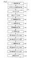
- 1 is a schematic cross sectional view schematically showing a structure of a silicon carbide semiconductor device in one embodiment of the present invention. It is a flowchart which shows schematically the manufacturing method of the silicon carbide semiconductor device in one embodiment of this invention. It is a flowchart which shows an interlayer insulation film formation process roughly. It is a flowchart which shows a wiring formation process schematically.
- 1 is a schematic cross sectional view schematically showing a first step of a method for manufacturing the silicon carbide semiconductor device in one embodiment of the present invention. It is a cross-sectional schematic diagram which shows schematically the 2nd process of the manufacturing method of the silicon carbide semiconductor device in one embodiment of this invention.
- FIG. 11 is a schematic cross sectional view schematically showing a third step of the method for manufacturing the silicon carbide semiconductor device in one embodiment of the present invention.
- FIG. 10 is a schematic cross sectional view schematically showing a fourth step of the method for manufacturing the silicon carbide semiconductor device in one embodiment of the present invention.
- FIG. 12 is a schematic cross sectional view schematically showing a fifth step of the method for manufacturing the silicon carbide semiconductor device in one embodiment of the present invention.
- FIG. 11 is a schematic cross sectional view schematically showing a sixth step of the method for manufacturing the silicon carbide semiconductor device in one embodiment of the present invention.
- FIG. 10 is a schematic cross sectional view schematically showing a seventh step of the method for manufacturing the silicon carbide semiconductor device in one embodiment of the present invention.
- FIG. 11 is a schematic cross sectional view schematically showing a ninth step of the method for manufacturing the silicon carbide semiconductor device in one embodiment of the present invention.
- FIG. 11 is a schematic cross sectional view schematically showing a tenth step of the method for manufacturing the silicon carbide semiconductor device in one embodiment of the present invention.
- It is a cross-sectional schematic diagram which shows schematically the 11th process of the manufacturing method of the silicon carbide semiconductor device in one embodiment of this invention.
- FIG. 11 is a schematic cross sectional view schematically showing a ninth step of the method for manufacturing the silicon carbide semiconductor device in one embodiment of the present invention.
- FIG. 11 is a schematic cross sectional view schematically showing a tenth step of the method for manufacturing the silicon carbide semiconductor device in one embodiment of the present invention.
- It is a cross-sectional schematic diagram which shows schematically the 11th process of
- FIG. 22 is a schematic cross sectional view schematically showing a thirteenth step of the method for manufacturing the silicon carbide semiconductor device in one embodiment of the present invention.
- FIG. 22 is a schematic cross sectional view schematically showing a fourteenth step of the method for manufacturing the silicon carbide semiconductor device in one embodiment of the present invention.
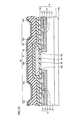
- It is a cross-sectional schematic diagram which shows schematically the modification of the 4th process of the manufacturing method of the silicon carbide semiconductor device in one embodiment of this invention.
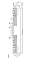
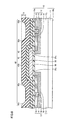
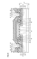
- MOSFET 1 includes a silicon carbide substrate 10, a gate insulating film 20, a gate electrode 30, an interlayer insulating film 40, a source electrode 50, a source electrode wiring 60a, a gate electrode wiring 60b, It mainly has a drain electrode 70, a back surface protection electrode 80, and a passivation layer 90.
- Silicon carbide substrate 10 includes a base substrate 11 and an epitaxial layer 12, and drift region 13, body region 14, source region 15, and p + region 16 are formed in epitaxial layer 12. .
- the base substrate 11 has an n-type conductivity (first conductivity type) by containing an n-type impurity such as N (nitrogen), for example.
- the epitaxial layer 12 is an epitaxial growth layer formed on the base substrate 11. Similar to base substrate 11, drift region 13 is a first conductivity type region having an n-type conductivity by containing an n-type impurity such as N (nitrogen), and its concentration is higher than that of base substrate 11. Is also low.
- Body region 14 includes first main surface 10a of silicon carbide substrate 10 and is formed in epitaxial layer 12 separately from each other.
- Body region 14 is a second conductivity type region whose conductivity type is p type (second conductivity type) by containing p type impurities such as Al (aluminum) and B (boron).
- the source region 15 (first conductivity type region) is a region whose conductivity type is n type (first conductivity type).
- Source region 15 includes first main surface 10 a and is formed in each body region 14 so as to be surrounded by body region 14.
- Source region 15 includes an n-type impurity such as P (phosphorus), for example, and has n-type conductivity like base substrate 11 and drift region 13. Further, the concentration of the n-type impurity contained in the source region 15 is higher than the concentration of the n-type impurity contained in the drift region 13.
- the source region 15 is separated from the drift region 13 by the body region 14.
- p + region 16 is formed in each body region 14 so as to be surrounded by body region 14 while including first main surface 10 a and adjacent to source region 15. Similar to body region 14, p + region 16 has a p-type conductivity by including a p-type impurity such as Al (aluminum) or B (boron). The impurity concentration of p + region 16 is higher than that of body region 14.
- Gate insulating film 20 is made of, for example, silicon dioxide, and is formed so as to extend from the upper surface of one source region 15 to the upper surface of the other source region 15 while being in contact with first main surface 10a. . Gate insulating film 20 is in contact with source region 15, body region 14, and drift region 13 on first main surface 10 a.
- the gate electrode 30 is formed to extend from the one source region 15 to the other source region 15 while being in contact with the gate insulating film 20.
- the gate electrode 30 is made of a conductor such as polysilicon to which impurities are added.
- Gate electrode 30 is formed to sandwich gate insulating film 20 with silicon carbide substrate 10.
- the gate electrode 30 is disposed to face the source region 15 and the body region 14 with the gate insulating film 20 interposed therebetween.
- the interlayer insulating film 40 is made of, for example, a material containing silicon dioxide, and is formed on the gate insulating film 20 so as to surround the gate electrode 30.
- the interlayer insulating film 40 is formed of a two-layer insulating film, and more preferably is formed of a three-layer insulating film.
- the interlayer insulating film 40 includes, for example, a first insulating film 41 in contact with the gate electrode 30 and the gate insulating film 20, and a second insulating film 42 in contact with the first insulating film 41. Has been.
- the first insulating film 41 is made of silicon dioxide not doped with impurities such as phosphorus (non-doped). Note that in this specification, an insulating film not doped with impurities means an insulating film having a doped impurity concentration of 1 mol% or less.
- the second insulating film 42 has a softening point lower than that of the first insulating film 41.
- the second insulating film 42 is, for example, silicon glass doped with phosphorus (PSG: Phosphorus Silicon Glass).
- the amount of phosphorus doped is, for example, about 7.5 mol% or more and 7.9 mol% or less.
- the thickness of the first insulating film 41 is 0.2 ⁇ m, for example, and the thickness of the second insulating film 42 is 0.8 ⁇ m, for example.
- the shoulder portion 42a of the interlayer insulating film 40 surrounding the outer peripheral corner portion 30a formed on the outer periphery of the gate electrode 30 is rounder than the outer peripheral corner portion 30a formed on the outer periphery of the gate electrode 30. It is preferable.
- the interlayer insulating film 40 is composed of the first insulating film 41 and the second insulating film 42
- the shoulder portion 42a of the second insulating film 42 may be rounder than 41a.
- a third insulating film 43 made of silicon dioxide may be disposed along the upper surface of second insulating film 42 whose shoulder 42 a has a round shape.
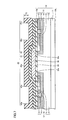
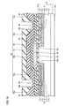
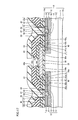
- a first recess 46 and a second recess 47 connected to the first recess 46 are formed in the interlayer insulating film 40 above the source region 15 and the p + region 16.
- the width W1 of the first recess 46 increases as the distance from the first main surface 10a increases.
- the width W ⁇ b> 2 of the second recess 47 is approximately the same as the narrowest width of the first recess 46.
- the width W2 of the second recess 47 is substantially constant along the normal direction of the first main surface 10a.
- the first inner wall surface 46 a (see FIG. 11) of the first recess 46 is formed by the second insulating film 42 of the interlayer insulating film 40.
- the second inner wall surface 47a (see FIG. 11) of the second recess 47 is formed by the second insulating film 42, the first insulating film 41, the gate insulating film 20, and the first main surface 10a.
- the first inner wall surface 46 a of the first recess 46 may be convex outward as viewed from the inside of the first recess 46.
- the angle formed by the first inner wall surface 46a of the first recess 46 and the first main surface 10a is greater than the angle formed by the second inner wall surface 47a of the second recess 47 and the first main surface 10a. May be larger.
- source electrode 50 (first electrode) is in contact with source region 15 and p + region 16 and is disposed inside second recess 47.
- the source electrode 50 is a film containing Ti, Al, and Si, and is made of, for example, a TiAlSi alloy.
- the source electrode 50 is a film containing Ni and Si, and may be, for example, a NiSi alloy.
- source electrode 50 is in ohmic contact with source region 15 and p + region 16.
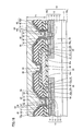
- a third recess 48 and a fourth recess 49 connected to the third recess 48 are formed.
- the width W3 of the third recess 48 increases as the distance from the first main surface 10a increases.
- the width W4 of the fourth recess 49 is about the same as the narrowest width of the third recess 48.
- the width W4 of the fourth recess 49 is substantially constant along the normal direction of the first main surface 10a.
- the third inner wall surface 48 a (see FIG. 17) of the third recess 48 is formed by the second insulating film 42 of the interlayer insulating film 40.
- a fourth inner wall surface 49 a (see FIG. 17) of the fourth recess 49 is formed by the second insulating film 42, the first insulating film 41, and the gate electrode 30.
- the third inner wall surface 48 a of the third recess 48 may be convex outward as viewed from the inside of the third recess 48.
- the angle formed between the third inner wall surface 48a of the third recess 48 and the first main surface 10a is greater than the angle formed between the fourth inner wall surface 49a of the fourth recess 49 and the first main surface 10a. May be larger.
- the source electrode wiring 60 a (first wiring) is formed so as to cover the source electrode 50 and the interlayer insulating film 40.
- the source electrode wiring 60 a contains, for example, aluminum and is electrically connected to the source electrode 50.
- the thickness T1 of the source electrode wiring 60a is, for example, 5 ⁇ m, preferably 2 ⁇ m or more and 10 ⁇ m or less, more preferably 3 ⁇ m or more and 7 ⁇ m or less. For example, a large current of about 1000 A / cm 2 can be passed through the source electrode wiring 60a.
- the source electrode wiring 60 a is disposed in contact with each of the first inner wall surface 46 a of the first recess 46 and the second inner wall surface 47 a of the second recess 47.
- source electrode interconnection 60 a includes first metal layer 61 a disposed in contact with upper surface 42 b of interlayer insulating film 40, first inner wall surface 46 a of first recess 46 and source electrode 50. .
- the first metal layer 61a is preferably made of Ti (titanium). More preferably, the source electrode wiring 60a has a second metal layer 62a disposed on and in contact with the first metal layer 61a.
- the second metal layer 62a is preferably made of TiN (titanium nitride) or TiW (titanium tungsten).
- the source electrode wiring 60a has a third metal layer 63a disposed on and in contact with the second metal layer 62a.
- the third metal layer 63a is preferably made of AlSiCu (aluminum silicon copper).
- the source electrode wiring 60 a is disposed inside each of the first recess 46 and the second recess 47.
- Each of the first metal layer 61 a, the second metal layer 62 a, and the third metal layer 63 a may be disposed in the first recess 46 or may be disposed in the second recess 47. Alternatively, it may be arranged inside each of the first recess 46 and the second recess 47.
- the source electrode wiring 60 a has a metal layer 64 sandwiched between the interlayer insulating film 40 and the first metal layer 61.
- the metal layer 64 is preferably made of TiN (titanium nitride) or TiW (titanium tungsten).
- the metal layer 64 may be in contact with the source electrode 50 and the gate insulating film 20.
- the metal layer 64 is disposed in contact with the second inner wall surface 47 a of the second recess 47.
- the gate electrode wiring 60 b (second wiring) is formed so as to cover the gate electrode 30 and the interlayer insulating film 40.
- Gate electrode interconnection 60b includes, for example, aluminum and is electrically connected to gate electrode 30.
- the gate electrode wiring 60 b is disposed inside the third recess 48 and the fourth recess 49.
- the gate electrode wiring 60b includes a first metal layer 61b disposed in contact with the third inner wall surface 48a of the third recess 48, the fourth inner wall surface 49a of the fourth recess 49, and the gate electrode 30. Is included.
- the first metal layer 61b is preferably made of Ti (titanium).
- the gate electrode wiring 60b preferably has a second metal layer 62b disposed on and in contact with the first metal layer 61b.
- the second metal layer 62b is preferably made of TiN (titanium nitride) or TiW (titanium tungsten).
- the gate electrode wiring 60b preferably has a third metal layer 63b in contact with the second metal layer 62b.
- the third metal layer 63b is preferably made of AlSiCu (aluminum silicon copper).
- Drain electrode 70 is formed in contact with second main surface 10b of silicon carbide substrate 10. Similarly to the source electrode 50, the drain electrode 70 may be made of, for example, a TiAlSi alloy, or may be made of, for example, a NiSi alloy. The drain electrode 70 is electrically connected to the base substrate 11. The back surface protection electrode 80 is provided in contact with the drain electrode 70. The back surface protective electrode 80 may be made of, for example, Ti (titanium), Ni (nickel), Ag (silver), or an alloy made of them.
- the passivation layer 90 is formed so as to insulate the source electrode wiring 60a and the gate electrode wiring 60b.
- the passivation layer 90 is preferably made of SiN (silicon nitride) or silicon dioxide.
- MOSFET 1 as the silicon carbide semiconductor device according to the present embodiment.
- body region 14 drifts in a state where the voltage applied to gate electrode 30 is less than the threshold voltage, that is, in the off state, even if a voltage is applied between source electrode 50 and drain electrode 70.
- the pn junction formed with the region 13 is reverse-biased and becomes non-conductive.
- an inversion layer is formed in the body region 14.
- the source region 15 and the drift region 13 are electrically connected, and a current flows between the source electrode 50 and the drain electrode 70.
- the MOSFET 1 operates.
- MOSFET 1 is manufactured as the silicon carbide semiconductor device according to the present embodiment.
- a silicon carbide substrate preparation step (S10) is performed.
- steps (S11) to (S14) described below are performed to prepare silicon carbide substrate 10 made of silicon carbide.
- a base substrate preparation step is performed.
- an ingot (not shown) made of hexagonal silicon carbide of polytype 4H is sliced to prepare base substrate 11 having a conductivity type of n type (first conductivity type).
- an epitaxial growth layer forming step is performed.
- an epitaxial layer 12 having an n conductivity type is formed on base substrate 11 by epitaxial growth.
- silicon carbide substrate 10 having first main surface 10a and second main surface 10b facing each other is formed.
- an ion implantation step is performed.
- Al (aluminum) ions are implanted into a region including first main surface 10a of silicon carbide substrate 10, so that epitaxial layer 12 is filled.
- Body region 14 having a p-type conductivity (second conductivity type) is formed.
- P (phosphorus) ions are implanted into the body region 14 at a depth shallower than the implantation depth of the Al ions, thereby forming the source region 15 whose conductivity type is n-type.
- Al ions are further implanted into body region 14 to form p + region 16 adjacent to source region 15 and having the same depth as source region 15 and having a conductivity type of p type. It is formed.
- a region where none of the body region 14, the source region 15, and the p + region 16 is formed becomes a drift region 13.
- an activation annealing step is performed as a step (S14).
- this step (S14) for example, by heating silicon carbide substrate 10 to about 1800 ° C. in an argon atmosphere, the impurities introduced in the above step (S13) are activated. As a result, desired carriers are generated in the region where the impurity is introduced.
- silicon carbide substrate 10 having an active region formed by introducing impurities is prepared.
- a gate insulating film forming step is performed.
- silicon carbide substrate 10 is heated in an atmosphere containing oxygen, for example, so as to be in contact with first main surface 10a of silicon carbide substrate 10 and made of silicon dioxide.
- a gate insulating film 20 is formed.
- a gate electrode forming step is performed as a step (S30).
- gate electrode 30 made of polysilicon containing an impurity such as phosphorus is brought into contact with gate insulating film 20 by, for example, LP-CVD (Low Pressure Chemical Vapor Deposition) method. Formed.
- LP-CVD Low Pressure Chemical Vapor Deposition
- the first main surface 10a and the second main surface 10b that face each other are provided, the gate insulating film 20 is provided in contact with the first main surface 10a, and the gate electrode 30 is in contact with the gate insulating film 20.
- silicon carbide substrate 10 including source region 15 which is a first conductivity type region in contact with first main surface 10a is prepared.
- interlayer insulating film 40 is formed in contact with gate electrode 30 and gate insulating film 20 so as to surround gate electrode 30, for example, by P (Plasma) -CVD. Is done.
- the interlayer insulating film 40 includes a first insulating film 41 and a second insulating film 42 having a softening point lower than that of the first insulating film 41.
- the first insulating film 41 covers the gate electrode 30 and is formed in contact with the gate electrode 30 and the gate insulating film 20.
- the first insulating film 41 is made of, for example, silicon dioxide not doped with impurities such as phosphorus (non-doped), and the second insulating film 42 is made of, for example, silicon glass (PSG) doped with phosphorus.
- PSG silicon glass
- a step of reducing the step of the upper surface 42b of the interlayer insulating film 40 by heating the interlayer insulating film 40 including the first insulating film 41 and the second insulating film 42 is performed.
- the silicon carbide substrate 10 on which the interlayer insulating film 40 including the first insulating film 41 and the second insulating film 42 is formed is heated to, for example, 1000 ° C.
- the insulating film 42 is softened and deformed.
- the shape of the shoulder 42a of the second insulating film 42 is deformed so as to be rounded.
- the step of the shoulder 42a of the second insulating film 42 is reduced from the step T2 to the step T3.
- the temperature for heating silicon carbide substrate 10 on which interlayer insulating film 40 including first insulating film 41 and second insulating film 42 is formed is preferably equal to or lower than the softening point of first insulating film 41. And above the softening point of the second insulating film 42.
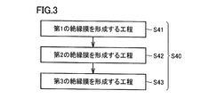
- the step of forming an interlayer insulating film (S40) includes a step of forming a first insulating film (S41), a step of forming a second insulating film (S42), A step of forming an insulating film (S43).
- the second insulating film 42 is formed on the first insulating film 41.
- the third insulating film 43 is disposed in contact with the surface of the second insulating film 42 as shown in FIG. It may be.
- the third insulating film 43 is made of, for example, silicon dioxide. The thickness of the third insulating film 43 may be smaller than the thickness of the second insulating film 42.
- a mask layer forming step is performed.
- first mask layer 45 made of, for example, a resist is formed in contact with interlayer insulating film 40.
- first mask layer 45 is patterned to have openings on source region 15 and p + region 16.
- a first isotropic etching step is performed.
- this step (S60) referring to FIG. 10, isotropic with respect to second insulating film 42 of interlayer insulating film 40 using first mask layer 45 formed in the mask layer forming step as a mask.
- Etching is performed.
- a first recess 46 having a first inner wall surface 46 a is formed in the second insulating film 42 of the interlayer insulating film 40.
- the first inner wall surface 46 a of the first recess 46 has a convex shape outward when viewed from the inside of the first recess 46.
- Isotropic etching is, for example, wet etching.
- the silicon carbide substrate 10 on which the first mask layer 45 is formed is immersed in a chemical solution made of buffered hydrofluoric acid (115UBHF) containing a surfactant for about 10 seconds to 300 seconds at room temperature, thereby providing interlayer insulation.
- the second insulating film 42 of the film 40 is isotropically etched.
- the isotropic etching may be dry etching.
- a first anisotropic etching step is performed.
- this step (S70) referring to FIG. 11, after the first isotropic etching step, interlayer insulation is performed using the first mask layer 45 used in the first isotropic etching step.
- the anisotropic etching is performed on the second insulating film 42, the first insulating film 41, and the gate insulating film 20 of the film 40.
- source region 15 and p + region 16 of silicon carbide substrate 10 are exposed from gate insulating film 20, are connected to first recess 46, and second inner wall surface 47 a is a first portion of interlayer insulating film 40.
- a second recess 47 formed by the insulating film 41, the second insulating film 42, the gate insulating film 20, and the first main surface 10a is formed.
- the width W2 of the second recess 47 has substantially the same value along the normal direction of the first main surface 10a.
- Anisotropic etching is, for example, dry etching.
- the silicon carbide substrate 10 on which the first mask layer 45 is formed is placed in a chamber having a pressure of 100 mTorr or more and 500 mTorr or less, and a CF 4 gas is used and RF (Radio Frequency) power is 100 W or more and 1500 W or less.
- anisotropic etching is performed on the second insulating film 42, the first insulating film 41, and the gate insulating film 20 of the interlayer insulating film 40.
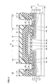
- a metal layer forming step is performed.
- the upper surface 46b of the second insulating film 42 of the interlayer insulating film 40 is formed, for example, by sputtering.
- the first inner wall surface 46a of the first recess 46, the second inner wall surface 47a of the second recess 47, the source region 15 and the metal layer 64 in contact with the p + region 16 are formed.
- the metal layer 64 is preferably a film containing Ti, for example, a film made of TiN or TiW.
- the thickness of the metal layer 64 is, for example, about 0.025 ⁇ m or more and 0.15 ⁇ m or less.
- an etching process is performed.
- the etching process referring to FIG. 13, by performing dry etching on silicon carbide substrate 10, the upper surface of interlayer insulating film 40, first inner wall surface 46 a of first recess 46, and source region 15 are formed.
- the metal layer 64 formed on the p + region 16 is removed, and the metal layer 64 formed on the second inner wall surface 47a of the second recess 47 remains.
- a source electrode forming step is performed as a step (S80).
- source electrode 50 as a first electrode in contact with source region 15 (first conductivity type region) and p + region 16 is formed.
- a metal film containing, for example, Ti, Al, and Si is formed in contact with source region 15, p + region 16, and second metal layer 62 by sputtering.
- the metal film is alloyed, and source electrode 50 that is in ohmic contact with silicon carbide substrate 10 is formed.
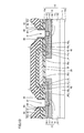
- a second isotropic etching step is performed.
- second mask layer 55 made of, for example, a resist is formed on and in contact with interlayer insulating film 40.
- the second mask layer 55 is patterned so as to have an opening above the gate electrode 30.
- isotropic etching is performed on second insulating film 42 of interlayer insulating film 40 disposed on gate electrode 30 using second mask layer 55 as a mask. Done.
- a third recess 48 having a third inner wall surface 48 a is formed in the second insulating film 42 of the interlayer insulating film 40.
- the third inner wall surface 48 a of the third recess 48 has a convex shape outward when viewed from the inside of the first recess 46.
- Isotropic etching is, for example, wet etching.
- the conditions for the second isotropic etching are substantially the same as the conditions for the first isotropic etching.
- a second anisotropic etching step is performed.
- this step (S100) referring to FIG. 17, after the second isotropic etching step, gate electrode is used by using second mask layer 55 used in the second isotropic etching step.
- the anisotropic etching is performed on the second insulating film 42 and the first insulating film 41 of the interlayer insulating film 40 disposed on the substrate 30.
- the gate electrode 30 is exposed from the interlayer insulating film 40, is connected to the third recess 48, and the fourth inner wall surface 49 a is the first insulating film 41 and the second insulating film 42 of the interlayer insulating film 40.
- a fourth recess 49 formed by the gate electrode 30 is formed.
- the width W4 of the fourth recess 49 is substantially the same value along the normal direction of the first main surface 10a.
- Anisotropic etching is, for example, dry etching.
- the conditions for the second anisotropic etching are substantially the same as the conditions for the first anisotropic etching.
- a wiring formation step is performed.
- wiring 60 is formed which is disposed inside first recess 46 and second recess 47 and is in contact with source region 15 and p + region 16.
- a step of forming a first metal layer (S111), a step of forming a second metal layer (S112), and a third metal layer are formed. It is preferable to have the process (S113) to perform.
- first metal layer in contact with second insulating film 42 and first insulating film 41 of interlayer insulating film 40, gate electrode 30, source electrode 50 and metal layer 64 is first formed by sputtering, for example. 61 is formed.
- the first metal layer 61 is made of, for example, Ti (titanium).
- the second metal layer 62 is formed on the first metal layer 61.
- the second metal layer 62 is made of, for example, TiN (titanium nitride) or TiW (titanium tungsten).
- a third metal layer 63 is formed on and in contact with the second metal layer 62.
- Third metal layer 63 preferably contains Al, Si, and Cu, and is made of, for example, an AlSiCu alloy.
- the thickness T1 of the wiring 60 is preferably 2 ⁇ m or more and 10 ⁇ m or less, more preferably 3 ⁇ m or more and 7 ⁇ m or less, for example, 5 ⁇ m.
- the wiring 60 includes a first sidewall surface 46a of the first recess 46, a second sidewall surface 47a of the second recess 47, a third sidewall surface 48a of the third recess 48, and a fourth recess. 49 in contact with the fourth side wall surface 49a.
- wiring 60 is patterned to form source electrode wiring 60 a and gate electrode wiring 60 b that are insulated from each other by passivation layer 90.
- the source electrode wiring 60 a is formed so as to be in contact with the first side wall surface 46 a of the first recess 46 and the second side wall surface 47 a of the second recess 47 and to be electrically connected to the source electrode 50.
- the gate electrode wiring 60 b is formed so as to be in contact with the third sidewall surface 48 a of the third recess 48 and the fourth sidewall surface 49 a of the fourth recess 49 and to be electrically connected to the gate electrode 30.
- MOSFET 1 according to the present embodiment is manufactured.
- the third recess 48 and the fourth recess in which the gate electrode wiring 60b is disposed after the first recess 46 and the second recess 47 in which the source electrode wiring 60a is disposed, the third recess 48 and the fourth recess in which the gate electrode wiring 60b is disposed.
- the recess 49 is formed has been described, the third recess in which the gate electrode wiring 60b is disposed before the first recess 46 and the second recess 47 in which the source electrode wiring 60a is disposed is formed.
- 48 and a fourth recess 49 may be formed.
- the 1st recessed part 46 and the 3rd recessed part 48 may be formed simultaneously.
- a first mask layer 45 having openings above the gate electrode 30 and the source electrode 50 is formed, and the first mask is formed.
- anisotropic etching is performed on the interlayer insulating film 40 using the layer 45, a first recess 46 and a third recess 48 are formed in the interlayer insulating film 40.
- anisotropic etching is performed on the interlayer insulating film 40 and the gate insulating film 20 above the source region 15 and the p + region 16 to form the second recess 47.
- a fourth recess 49 is formed in the interlayer insulating film 40 above the gate electrode 30.
- the second concave portion 47 and the fourth concave portion 49 may be formed at the same time or may be formed separately.
- MOSFET is described as an example of the silicon carbide semiconductor device, but the silicon carbide semiconductor device may be, for example, an IGBT (Insulated Gate Bipolar Transistor).
- the silicon carbide semiconductor device is an IGBT
- the first electrode 50 is an emitter electrode
- the first wiring 60a is an emitter electrode wiring.
- the n-type and the p-type are described as the first conductivity type and the second conductivity type, respectively.
- the n-type and the p-type may be the second conductivity type and the first conductivity type, respectively. Good.
- the first recess 46 is formed in the interlayer insulating film 40 by performing isotropic etching, and then the source region 15 is formed by performing anisotropic etching. By exposing, the second recess 47 is formed. A source electrode wiring 60 a that is disposed in contact with the first inner wall surface 46 a of the first recess 46 and the second inner wall surface 47 a of the second recess 47 and is connected to the source electrode 50 is formed. By the isotropic etching, a first recess 46 having a rounded first inner wall surface 46 a is formed in the interlayer insulating film 40.
- the source electrode wiring 60a is disposed in contact with the first inner wall surface 46a, the formation of a cavity in the source electrode wiring 60a can be suppressed. As a result, the source electrode wiring 60a can be prevented from being disconnected when a large current is passed through the source electrode wiring 60a, so that the reliability of the source electrode wiring 60a can be improved.
- the step of forming interlayer insulating film 40 includes the step of reducing step T2 of upper surface 42b of interlayer insulating film 40 by heating interlayer insulating film 40. Including. Thereby, since the wiring 60 is formed on the interlayer insulating film 40 in which the step T2 of the upper surface 42b is reduced, it is possible to efficiently suppress the generation of a cavity inside the wiring 60.
- the step of forming interlayer insulating film 40 includes the step of forming first insulating film 41 in contact with gate electrode 30 and not doped with impurities, Forming a second insulating film 42 covering the first insulating film 41 and having a softening point lower than that of the first insulating film 41 and doped with impurities.
- step difference T2 of the upper surface 42b of the interlayer insulation film 40 can be reduced at low temperature.
- the first insulating film 41 is not doped with impurities, for example, impurities such as phosphorus diffuse to the interface between the gate insulating film 20 and the silicon carbide substrate 10 and the threshold voltage of the gate voltage varies. Can be suppressed.
- the step of forming interlayer insulating film 40 includes the step of forming third insulating film 43 that covers second insulating film 42 and is made of silicon dioxide. Further included.
- the third insulating film 43 made of silicon dioxide has good adhesion to the wiring 60. Therefore, by forming the third insulating film 43, it is possible to improve the contact of the wiring 60 formed on the third insulating film 43.
- the first isotropic etching is wet etching.
- the 1st recessed part 46 which becomes large as the width W1 leaves
- the first anisotropic etching is dry etching.
- the 2nd recessed part 47 whose width W2 is substantially the same can be formed efficiently along the normal line direction of the 1st main surface 10a.
- gate electrode wiring 60b is formed in contact with third inner wall surface 48a of third recess 48 formed by isotropic etching, gate electrode It is possible to suppress the formation of a cavity inside the wiring 60b. As a result, it is possible to suppress the disconnection of the gate electrode wiring 60b when a current is passed through the gate electrode wiring 60b, so that the reliability of the gate electrode wiring 60b can be improved.
- the thickness T1 of the wiring 60 is not less than 2 ⁇ m and not more than 10 ⁇ m.
- the thickness of the wiring 60 is 2 ⁇ m or more, a large current can flow through the wiring 60. If the thickness T1 of the wiring 60 is 10 ⁇ m or less, the workability of the wiring 60 can be improved.
- the step of forming wiring 60 includes the step of forming first metal layer 61 that is in contact with interlayer insulating film 40 and made of titanium.
- first metal layer 61 made of titanium in contact with the interlayer insulating film 40, the adhesion of the wiring 60 to the interlayer insulating film 40 can be improved.
- the step of forming wiring 60 forms second metal layer 62 in contact with first metal layer 61 and made of titanium nitride or titanium tungsten.
- the method further includes the step of: Thereby, in the case where the third metal layer 63 containing aluminum is formed on the second metal layer 62, it is possible to prevent aluminum from entering the gate electrode 30.
- first recess 46 is formed such that width W1 increases as the distance from first main surface 10a increases, and second recess 47 is formed in first recess 46. It is formed by connecting.
- the source electrode wiring 60a is disposed in contact with the first inner wall surface 46a and the second inner wall surface 47a.
- the source electrode wiring 60a is disposed in contact with the first inner wall surface 46a of the first recess 46 whose width W1 increases as the distance from the first main surface 10a increases.
- the source electrode wiring 60a can be prevented from being disconnected when a large current is passed through the source electrode wiring 60a, so that the reliability of the source electrode wiring 60a can be improved.
- the shoulder portion 42 a surrounding the outer peripheral corner portion 30 a of the gate electrode 30 on the upper surface 42 b of the interlayer insulating film 40 is rounder than the outer peripheral corner portion 30 a of the gate electrode 30. This effectively suppresses the formation of a cavity in the source electrode wiring 60a formed in the vicinity of the shoulder portion 42a surrounding the outer peripheral corner portion 30a of the gate electrode 30 on the upper surface 42b of the interlayer insulating film 40. Can do.
- gate electrode wiring 60b is arranged in contact with third inner wall surface 48a of third recess 48 in which width W3 increases as the distance from first main surface 10a increases.
- the formation of a cavity inside the gate electrode wiring 60b can be suppressed.
- the interlayer insulating film 40 covers the first insulating film 41 that is in contact with the gate electrode 30 and is not doped with impurities, and the first insulating film 41. And a second insulating film 42 having a softening point lower than that of the insulating film 41 and doped with impurities.
- step difference T2 of the upper surface 42b of the interlayer insulation film 40 can be reduced at low temperature.
- the first insulating film 41 is not doped with impurities, for example, impurities such as phosphorus diffuse to the interface between the gate insulating film 20 and the silicon carbide substrate 10 and the threshold voltage of the gate voltage varies. Can be suppressed.
- interlayer insulating film 40 further includes a third insulating film 43 that covers second insulating film 42 and is made of silicon dioxide.
- the third insulating film 43 made of silicon dioxide has good adhesion with the source electrode wiring 60a and the gate electrode wiring 60b. Therefore, it is possible to improve the contact between the source electrode wiring 60a and the gate electrode wiring 60b formed on the third insulating film 43.
- the thickness T1 of the source electrode wiring 60a is not less than 2 ⁇ m and not more than 10 ⁇ m.
- the thickness T1 of the source electrode wiring 60a is 2 ⁇ m or more, a large current can flow through the source electrode wiring 60a. If the thickness T1 of the source electrode wiring 60a is 10 ⁇ m or less, the workability of the source electrode wiring 60a can be improved.
- source electrode wiring 60a includes first metal layer 61 in contact with interlayer insulating film 40 and made of titanium.
- first metal layer 61 made of titanium By disposing the first metal layer 61 made of titanium in contact with the interlayer insulating film 40, the adhesion of the source electrode wiring 60a to the interlayer insulating film 40 can be improved.
- source electrode wiring 60a further includes second metal layer 62 in contact with first metal layer 61 and made of titanium nitride or titanium tungsten.
- second metal layer 62 in contact with first metal layer 61 and made of titanium nitride or titanium tungsten.
Landscapes
- Engineering & Computer Science (AREA)
- Microelectronics & Electronic Packaging (AREA)
- Power Engineering (AREA)
- Physics & Mathematics (AREA)
- Condensed Matter Physics & Semiconductors (AREA)
- General Physics & Mathematics (AREA)
- Computer Hardware Design (AREA)
- Manufacturing & Machinery (AREA)
- Ceramic Engineering (AREA)
- Chemical & Material Sciences (AREA)
- Crystallography & Structural Chemistry (AREA)
- Chemical Kinetics & Catalysis (AREA)
- General Chemical & Material Sciences (AREA)
- Inorganic Chemistry (AREA)
- Geometry (AREA)
- Electrodes Of Semiconductors (AREA)
- Internal Circuitry In Semiconductor Integrated Circuit Devices (AREA)
Priority Applications (3)
| Application Number | Priority Date | Filing Date | Title |
|---|---|---|---|
| US14/766,955 US9728607B2 (en) | 2013-03-08 | 2014-01-17 | Silicon carbide semiconductor device and method for manufacturing silicon carbide semiconductor device |
| CN201480007910.0A CN105074886B (zh) | 2013-03-08 | 2014-01-17 | 碳化硅半导体器件及其制造方法 |
| EP14761228.7A EP2966676B1 (en) | 2013-03-08 | 2014-01-17 | Silicon-carbide semiconductor device and manufacturing method therefor |
Applications Claiming Priority (2)
| Application Number | Priority Date | Filing Date | Title |
|---|---|---|---|
| JP2013-046894 | 2013-03-08 | ||
| JP2013046894A JP6297783B2 (ja) | 2013-03-08 | 2013-03-08 | 炭化珪素半導体装置およびその製造方法 |
Publications (1)
| Publication Number | Publication Date |
|---|---|
| WO2014136478A1 true WO2014136478A1 (ja) | 2014-09-12 |
Family
ID=51491009
Family Applications (1)
| Application Number | Title | Priority Date | Filing Date |
|---|---|---|---|
| PCT/JP2014/050798 WO2014136478A1 (ja) | 2013-03-08 | 2014-01-17 | 炭化珪素半導体装置およびその製造方法 |
Country Status (5)
| Country | Link |
|---|---|
| US (1) | US9728607B2 (zh) |
| EP (1) | EP2966676B1 (zh) |
| JP (1) | JP6297783B2 (zh) |
| CN (1) | CN105074886B (zh) |
| WO (1) | WO2014136478A1 (zh) |
Families Citing this family (14)
| Publication number | Priority date | Publication date | Assignee | Title |
|---|---|---|---|---|
| DZ2805A1 (fr) | 1998-06-02 | 2005-01-30 | Cadus Pharmaceutical Corp | Composition à pyrroloÄ2,,3dÜ pyrimidine et leurs usages. |
| US9991399B2 (en) * | 2012-10-04 | 2018-06-05 | Cree, Inc. | Passivation structure for semiconductor devices |
| JP6480860B2 (ja) * | 2013-03-29 | 2019-03-13 | 富士電機株式会社 | 半導体装置および半導体装置の製造方法 |
| JP6267624B2 (ja) * | 2014-10-24 | 2018-01-24 | 住友電気工業株式会社 | 炭化珪素半導体装置 |
| JP2017139292A (ja) * | 2016-02-02 | 2017-08-10 | 富士電機株式会社 | 半導体装置及びその製造方法 |
| DE102016104788B4 (de) * | 2016-03-15 | 2019-06-19 | Infineon Technologies Ag | Halbleitervorrichtung mit einer Metalladhäsions- und Barrierestruktur und Verfahren zum Herstellen einer Halbleitervorrichtung |
| JP2017168681A (ja) * | 2016-03-16 | 2017-09-21 | 富士電機株式会社 | 半導体装置および半導体装置の製造方法 |
| US10116303B2 (en) * | 2016-07-01 | 2018-10-30 | Toyota Motor Engineering & Manufacturing North America, Inc. | Parallel devices having balanced switching current and power |
| JP2019009357A (ja) * | 2017-06-27 | 2019-01-17 | 株式会社 日立パワーデバイス | 半導体装置およびその製造方法 |
| CN109360785A (zh) * | 2018-09-27 | 2019-02-19 | 上海华虹宏力半导体制造有限公司 | Mos器件的制造方法 |
| JP7143729B2 (ja) * | 2018-11-09 | 2022-09-29 | 株式会社デンソー | 半導体装置 |
| JP7180425B2 (ja) * | 2019-02-06 | 2022-11-30 | 住友電気工業株式会社 | 炭化珪素半導体装置 |
| US11205720B2 (en) * | 2019-05-30 | 2021-12-21 | Rohm Co., Ltd. | Semiconductor device with contact plugs |
| JP7444084B2 (ja) * | 2021-01-14 | 2024-03-06 | 三菱電機株式会社 | 半導体装置 |
Citations (7)
| Publication number | Priority date | Publication date | Assignee | Title |
|---|---|---|---|---|
| JPH10321732A (ja) * | 1997-03-18 | 1998-12-04 | Nippon Steel Corp | 半導体装置及びその製造方法 |
| JP2003318129A (ja) * | 2002-04-19 | 2003-11-07 | Denso Corp | 半導体装置の製造方法及びその製造方法により得られる半導体装置 |
| JP2006173289A (ja) * | 2004-12-15 | 2006-06-29 | Fuji Electric Device Technology Co Ltd | 半導体装置の製造方法 |
| JP2007059954A (ja) * | 2006-12-05 | 2007-03-08 | Toshiba Corp | 半導体装置 |
| JP2008112824A (ja) * | 2006-10-30 | 2008-05-15 | Denso Corp | 炭化珪素半導体装置の製造方法 |
| JP2010141028A (ja) * | 2008-12-10 | 2010-06-24 | Renesas Technology Corp | 半導体装置の製造方法 |
| JP2010147380A (ja) * | 2008-12-22 | 2010-07-01 | Denso Corp | 半導体装置の製造方法 |
Family Cites Families (17)
| Publication number | Priority date | Publication date | Assignee | Title |
|---|---|---|---|---|
| US4372034B1 (en) * | 1981-03-26 | 1998-07-21 | Intel Corp | Process for forming contact openings through oxide layers |
| US5077238A (en) * | 1988-05-18 | 1991-12-31 | Mitsubishi Denki Kabushiki Kaisha | Method of manufacturing a semiconductor device with a planar interlayer insulating film |
| US5006913A (en) * | 1988-11-05 | 1991-04-09 | Mitsubishi Denki Kabushiki Kaisha | Stacked type semiconductor device |
| JP2809018B2 (ja) * | 1992-11-26 | 1998-10-08 | 日本電気株式会社 | 半導体装置およびその製造方法 |
| KR960012252B1 (ko) * | 1993-03-05 | 1996-09-18 | 삼성전자 주식회사 | 반도체 메모리장치 |
| US5710070A (en) * | 1996-11-08 | 1998-01-20 | Chartered Semiconductor Manufacturing Pte Ltd. | Application of titanium nitride and tungsten nitride thin film resistor for thermal ink jet technology |
| JP4655340B2 (ja) * | 2000-07-10 | 2011-03-23 | 株式会社デンソー | 半導体装置の製造方法 |
| JP3559971B2 (ja) * | 2001-12-11 | 2004-09-02 | 日産自動車株式会社 | 炭化珪素半導体装置およびその製造方法 |
| US7217954B2 (en) * | 2003-03-18 | 2007-05-15 | Matsushita Electric Industrial Co., Ltd. | Silicon carbide semiconductor device and method for fabricating the same |
| US20060027833A1 (en) * | 2004-08-04 | 2006-02-09 | Nissan Motor Co., Ltd. | Silicon carbide semiconductor device and method of manufacturing the same |
| WO2009054140A1 (ja) * | 2007-10-24 | 2009-04-30 | Panasonic Corporation | 半導体素子およびその製造方法 |
| US7867852B2 (en) * | 2008-08-08 | 2011-01-11 | Alpha And Omega Semiconductor Incorporated | Super-self-aligned trench-dmos structure and method |
| US8362552B2 (en) * | 2008-12-23 | 2013-01-29 | Alpha And Omega Semiconductor Incorporated | MOSFET device with reduced breakdown voltage |
| JP5588670B2 (ja) * | 2008-12-25 | 2014-09-10 | ローム株式会社 | 半導体装置 |
| JP5551887B2 (ja) * | 2009-03-31 | 2014-07-16 | ラピスセミコンダクタ株式会社 | 半導体素子の製造方法 |
| KR20120014017A (ko) | 2009-05-11 | 2012-02-15 | 스미토모덴키고교가부시키가이샤 | 탄화규소 기판, 반도체 장치 및 탄화규소 기판의 제조 방법 |
| JP2011129750A (ja) * | 2009-12-18 | 2011-06-30 | Toyota Motor Corp | 高耐圧半導体素子の製造方法及びその構造 |
-
2013
- 2013-03-08 JP JP2013046894A patent/JP6297783B2/ja active Active
-
2014
- 2014-01-17 EP EP14761228.7A patent/EP2966676B1/en active Active
- 2014-01-17 CN CN201480007910.0A patent/CN105074886B/zh active Active
- 2014-01-17 WO PCT/JP2014/050798 patent/WO2014136478A1/ja active Application Filing
- 2014-01-17 US US14/766,955 patent/US9728607B2/en active Active
Patent Citations (7)
| Publication number | Priority date | Publication date | Assignee | Title |
|---|---|---|---|---|
| JPH10321732A (ja) * | 1997-03-18 | 1998-12-04 | Nippon Steel Corp | 半導体装置及びその製造方法 |
| JP2003318129A (ja) * | 2002-04-19 | 2003-11-07 | Denso Corp | 半導体装置の製造方法及びその製造方法により得られる半導体装置 |
| JP2006173289A (ja) * | 2004-12-15 | 2006-06-29 | Fuji Electric Device Technology Co Ltd | 半導体装置の製造方法 |
| JP2008112824A (ja) * | 2006-10-30 | 2008-05-15 | Denso Corp | 炭化珪素半導体装置の製造方法 |
| JP2007059954A (ja) * | 2006-12-05 | 2007-03-08 | Toshiba Corp | 半導体装置 |
| JP2010141028A (ja) * | 2008-12-10 | 2010-06-24 | Renesas Technology Corp | 半導体装置の製造方法 |
| JP2010147380A (ja) * | 2008-12-22 | 2010-07-01 | Denso Corp | 半導体装置の製造方法 |
Non-Patent Citations (1)
| Title |
|---|
| HIROYUKI MATSUNAMI: "Semiconductor SiC Technology and Applications", 30 September 2011, NIKKAN KOGYO SHIMBUN, LTD., pages: 358 - 365 |
Also Published As
| Publication number | Publication date |
|---|---|
| CN105074886A (zh) | 2015-11-18 |
| EP2966676A4 (en) | 2016-10-12 |
| CN105074886B (zh) | 2020-11-03 |
| JP6297783B2 (ja) | 2018-03-20 |
| JP2014175471A (ja) | 2014-09-22 |
| US20150372094A1 (en) | 2015-12-24 |
| US9728607B2 (en) | 2017-08-08 |
| EP2966676B1 (en) | 2020-10-28 |
| EP2966676A1 (en) | 2016-01-13 |
Similar Documents
| Publication | Publication Date | Title |
|---|---|---|
| JP6297783B2 (ja) | 炭化珪素半導体装置およびその製造方法 | |
| JP5525940B2 (ja) | 半導体装置および半導体装置の製造方法 | |
| US9024330B2 (en) | Semiconductor device and manufacturing method thereof | |
| US9613809B2 (en) | Method of manufacturing silicon carbide semiconductor device | |
| WO2014112204A1 (ja) | 炭化珪素半導体装置 | |
| EP2242107A1 (en) | Semiconductor device | |
| WO2013105353A1 (ja) | 半導体装置およびその製造方法 | |
| US20160163800A1 (en) | Semiconductor device and method of manufacturing the same | |
| JP5902116B2 (ja) | 半導体装置 | |
| JP2018082114A (ja) | 半導体装置の製造方法 | |
| JP2012243985A (ja) | 半導体装置及びその製造方法 | |
| WO2015012009A1 (ja) | 炭化珪素半導体装置およびその製造方法 | |
| JP7369601B2 (ja) | 半導体装置およびその製造方法 | |
| JP2015076592A (ja) | 炭化珪素半導体装置およびその製造方法 | |
| US10439027B2 (en) | Silicon carbide semiconductor device and method for manufacturing the same | |
| JP6183200B2 (ja) | 炭化珪素半導体装置およびその製造方法 | |
| US9263280B2 (en) | Semiconductor device with equipotential ring contact at curved portion of equipotential ring electrode and method of manufacturing the same | |
| WO2017051616A1 (ja) | 炭化珪素半導体装置およびその製造方法 | |
| JPWO2015166754A1 (ja) | 半導体装置 | |
| JP6295797B2 (ja) | 炭化珪素半導体装置およびその製造方法 | |
| JP2015204409A (ja) | 炭化珪素半導体装置およびその製造方法 | |
| KR102056356B1 (ko) | 전력 반도체 소자의 제조 방법 및 그에 따른 전력 반도체 소자 | |
| US20240186407A1 (en) | Semiconductor device and method of manufacturing semiconductor device |
Legal Events
| Date | Code | Title | Description |
|---|---|---|---|
| WWE | Wipo information: entry into national phase |
Ref document number: 201480007910.0 Country of ref document: CN |
|
| 121 | Ep: the epo has been informed by wipo that ep was designated in this application |
Ref document number: 14761228 Country of ref document: EP Kind code of ref document: A1 |
|
| WWE | Wipo information: entry into national phase |
Ref document number: 2014761228 Country of ref document: EP |
|
| WWE | Wipo information: entry into national phase |
Ref document number: 14766955 Country of ref document: US |
|
| NENP | Non-entry into the national phase |
Ref country code: DE |