WO2014038066A1 - パワー半導体装置 - Google Patents
パワー半導体装置 Download PDFInfo
- Publication number
- WO2014038066A1 WO2014038066A1 PCT/JP2012/072908 JP2012072908W WO2014038066A1 WO 2014038066 A1 WO2014038066 A1 WO 2014038066A1 JP 2012072908 W JP2012072908 W JP 2012072908W WO 2014038066 A1 WO2014038066 A1 WO 2014038066A1
- Authority
- WO
- WIPO (PCT)
- Prior art keywords
- power semiconductor
- capacitor
- semiconductor device
- stress relaxation
- lead frame
- Prior art date
Links
Images


Classifications
-
- H—ELECTRICITY
- H01—ELECTRIC ELEMENTS
- H01L—SEMICONDUCTOR DEVICES NOT COVERED BY CLASS H10
- H01L23/00—Details of semiconductor or other solid state devices
- H01L23/48—Arrangements for conducting electric current to or from the solid state body in operation, e.g. leads, terminal arrangements ; Selection of materials therefor
- H01L23/488—Arrangements for conducting electric current to or from the solid state body in operation, e.g. leads, terminal arrangements ; Selection of materials therefor consisting of soldered or bonded constructions
- H01L23/495—Lead-frames or other flat leads
- H01L23/49589—Capacitor integral with or on the leadframe
-
- H—ELECTRICITY
- H01—ELECTRIC ELEMENTS
- H01L—SEMICONDUCTOR DEVICES NOT COVERED BY CLASS H10
- H01L23/00—Details of semiconductor or other solid state devices
- H01L23/28—Encapsulations, e.g. encapsulating layers, coatings, e.g. for protection
- H01L23/31—Encapsulations, e.g. encapsulating layers, coatings, e.g. for protection characterised by the arrangement or shape
- H01L23/3107—Encapsulations, e.g. encapsulating layers, coatings, e.g. for protection characterised by the arrangement or shape the device being completely enclosed
-
- H—ELECTRICITY
- H01—ELECTRIC ELEMENTS
- H01L—SEMICONDUCTOR DEVICES NOT COVERED BY CLASS H10
- H01L23/00—Details of semiconductor or other solid state devices
- H01L23/48—Arrangements for conducting electric current to or from the solid state body in operation, e.g. leads, terminal arrangements ; Selection of materials therefor
- H01L23/488—Arrangements for conducting electric current to or from the solid state body in operation, e.g. leads, terminal arrangements ; Selection of materials therefor consisting of soldered or bonded constructions
- H01L23/492—Bases or plates or solder therefor
-
- H—ELECTRICITY
- H01—ELECTRIC ELEMENTS
- H01L—SEMICONDUCTOR DEVICES NOT COVERED BY CLASS H10
- H01L23/00—Details of semiconductor or other solid state devices
- H01L23/48—Arrangements for conducting electric current to or from the solid state body in operation, e.g. leads, terminal arrangements ; Selection of materials therefor
- H01L23/488—Arrangements for conducting electric current to or from the solid state body in operation, e.g. leads, terminal arrangements ; Selection of materials therefor consisting of soldered or bonded constructions
- H01L23/495—Lead-frames or other flat leads
- H01L23/49517—Additional leads
- H01L23/4952—Additional leads the additional leads being a bump or a wire
-
- H—ELECTRICITY
- H01—ELECTRIC ELEMENTS
- H01L—SEMICONDUCTOR DEVICES NOT COVERED BY CLASS H10
- H01L23/00—Details of semiconductor or other solid state devices
- H01L23/48—Arrangements for conducting electric current to or from the solid state body in operation, e.g. leads, terminal arrangements ; Selection of materials therefor
- H01L23/488—Arrangements for conducting electric current to or from the solid state body in operation, e.g. leads, terminal arrangements ; Selection of materials therefor consisting of soldered or bonded constructions
- H01L23/495—Lead-frames or other flat leads
- H01L23/49517—Additional leads
- H01L23/49531—Additional leads the additional leads being a wiring board
-
- H—ELECTRICITY
- H01—ELECTRIC ELEMENTS
- H01L—SEMICONDUCTOR DEVICES NOT COVERED BY CLASS H10
- H01L23/00—Details of semiconductor or other solid state devices
- H01L23/48—Arrangements for conducting electric current to or from the solid state body in operation, e.g. leads, terminal arrangements ; Selection of materials therefor
- H01L23/488—Arrangements for conducting electric current to or from the solid state body in operation, e.g. leads, terminal arrangements ; Selection of materials therefor consisting of soldered or bonded constructions
- H01L23/495—Lead-frames or other flat leads
- H01L23/49537—Plurality of lead frames mounted in one device
-
- H—ELECTRICITY
- H01—ELECTRIC ELEMENTS
- H01L—SEMICONDUCTOR DEVICES NOT COVERED BY CLASS H10
- H01L23/00—Details of semiconductor or other solid state devices
- H01L23/48—Arrangements for conducting electric current to or from the solid state body in operation, e.g. leads, terminal arrangements ; Selection of materials therefor
- H01L23/488—Arrangements for conducting electric current to or from the solid state body in operation, e.g. leads, terminal arrangements ; Selection of materials therefor consisting of soldered or bonded constructions
- H01L23/495—Lead-frames or other flat leads
- H01L23/49541—Geometry of the lead-frame
- H01L23/49562—Geometry of the lead-frame for devices being provided for in H01L29/00
-
- H—ELECTRICITY
- H01—ELECTRIC ELEMENTS
- H01L—SEMICONDUCTOR DEVICES NOT COVERED BY CLASS H10
- H01L23/00—Details of semiconductor or other solid state devices
- H01L23/48—Arrangements for conducting electric current to or from the solid state body in operation, e.g. leads, terminal arrangements ; Selection of materials therefor
- H01L23/488—Arrangements for conducting electric current to or from the solid state body in operation, e.g. leads, terminal arrangements ; Selection of materials therefor consisting of soldered or bonded constructions
- H01L23/495—Lead-frames or other flat leads
- H01L23/49575—Assemblies of semiconductor devices on lead frames
-
- H—ELECTRICITY
- H01—ELECTRIC ELEMENTS
- H01L—SEMICONDUCTOR DEVICES NOT COVERED BY CLASS H10
- H01L23/00—Details of semiconductor or other solid state devices
- H01L23/562—Protection against mechanical damage
-
- H—ELECTRICITY
- H05—ELECTRIC TECHNIQUES NOT OTHERWISE PROVIDED FOR
- H05K—PRINTED CIRCUITS; CASINGS OR CONSTRUCTIONAL DETAILS OF ELECTRIC APPARATUS; MANUFACTURE OF ASSEMBLAGES OF ELECTRICAL COMPONENTS
- H05K1/00—Printed circuits
- H05K1/18—Printed circuits structurally associated with non-printed electric components
- H05K1/182—Printed circuits structurally associated with non-printed electric components associated with components mounted in the printed circuit board, e.g. insert mounted components [IMC]
- H05K1/185—Components encapsulated in the insulating substrate of the printed circuit or incorporated in internal layers of a multilayer circuit
- H05K1/186—Components encapsulated in the insulating substrate of the printed circuit or incorporated in internal layers of a multilayer circuit manufactured by mounting on or connecting to patterned circuits before or during embedding
-
- H—ELECTRICITY
- H05—ELECTRIC TECHNIQUES NOT OTHERWISE PROVIDED FOR
- H05K—PRINTED CIRCUITS; CASINGS OR CONSTRUCTIONAL DETAILS OF ELECTRIC APPARATUS; MANUFACTURE OF ASSEMBLAGES OF ELECTRICAL COMPONENTS
- H05K3/00—Apparatus or processes for manufacturing printed circuits
- H05K3/10—Apparatus or processes for manufacturing printed circuits in which conductive material is applied to the insulating support in such a manner as to form the desired conductive pattern
- H05K3/103—Apparatus or processes for manufacturing printed circuits in which conductive material is applied to the insulating support in such a manner as to form the desired conductive pattern by bonding or embedding conductive wires or strips
-
- H—ELECTRICITY
- H01—ELECTRIC ELEMENTS
- H01L—SEMICONDUCTOR DEVICES NOT COVERED BY CLASS H10
- H01L2224/00—Indexing scheme for arrangements for connecting or disconnecting semiconductor or solid-state bodies and methods related thereto as covered by H01L24/00
- H01L2224/01—Means for bonding being attached to, or being formed on, the surface to be connected, e.g. chip-to-package, die-attach, "first-level" interconnects; Manufacturing methods related thereto
- H01L2224/02—Bonding areas; Manufacturing methods related thereto
- H01L2224/04—Structure, shape, material or disposition of the bonding areas prior to the connecting process
- H01L2224/05—Structure, shape, material or disposition of the bonding areas prior to the connecting process of an individual bonding area
- H01L2224/0554—External layer
- H01L2224/05599—Material
- H01L2224/056—Material with a principal constituent of the material being a metal or a metalloid, e.g. boron [B], silicon [Si], germanium [Ge], arsenic [As], antimony [Sb], tellurium [Te] and polonium [Po], and alloys thereof
- H01L2224/05617—Material with a principal constituent of the material being a metal or a metalloid, e.g. boron [B], silicon [Si], germanium [Ge], arsenic [As], antimony [Sb], tellurium [Te] and polonium [Po], and alloys thereof the principal constituent melting at a temperature of greater than or equal to 400°C and less than 950°C
- H01L2224/05624—Aluminium [Al] as principal constituent
-
- H—ELECTRICITY
- H01—ELECTRIC ELEMENTS
- H01L—SEMICONDUCTOR DEVICES NOT COVERED BY CLASS H10
- H01L2224/00—Indexing scheme for arrangements for connecting or disconnecting semiconductor or solid-state bodies and methods related thereto as covered by H01L24/00
- H01L2224/01—Means for bonding being attached to, or being formed on, the surface to be connected, e.g. chip-to-package, die-attach, "first-level" interconnects; Manufacturing methods related thereto
- H01L2224/42—Wire connectors; Manufacturing methods related thereto
- H01L2224/44—Structure, shape, material or disposition of the wire connectors prior to the connecting process
- H01L2224/45—Structure, shape, material or disposition of the wire connectors prior to the connecting process of an individual wire connector
- H01L2224/45001—Core members of the connector
- H01L2224/45099—Material
- H01L2224/451—Material with a principal constituent of the material being a metal or a metalloid, e.g. boron (B), silicon (Si), germanium (Ge), arsenic (As), antimony (Sb), tellurium (Te) and polonium (Po), and alloys thereof
- H01L2224/45117—Material with a principal constituent of the material being a metal or a metalloid, e.g. boron (B), silicon (Si), germanium (Ge), arsenic (As), antimony (Sb), tellurium (Te) and polonium (Po), and alloys thereof the principal constituent melting at a temperature of greater than or equal to 400°C and less than 950°C
- H01L2224/45124—Aluminium (Al) as principal constituent
-
- H—ELECTRICITY
- H01—ELECTRIC ELEMENTS
- H01L—SEMICONDUCTOR DEVICES NOT COVERED BY CLASS H10
- H01L2224/00—Indexing scheme for arrangements for connecting or disconnecting semiconductor or solid-state bodies and methods related thereto as covered by H01L24/00
- H01L2224/01—Means for bonding being attached to, or being formed on, the surface to be connected, e.g. chip-to-package, die-attach, "first-level" interconnects; Manufacturing methods related thereto
- H01L2224/42—Wire connectors; Manufacturing methods related thereto
- H01L2224/44—Structure, shape, material or disposition of the wire connectors prior to the connecting process
- H01L2224/45—Structure, shape, material or disposition of the wire connectors prior to the connecting process of an individual wire connector
- H01L2224/45001—Core members of the connector
- H01L2224/45099—Material
- H01L2224/451—Material with a principal constituent of the material being a metal or a metalloid, e.g. boron (B), silicon (Si), germanium (Ge), arsenic (As), antimony (Sb), tellurium (Te) and polonium (Po), and alloys thereof
- H01L2224/45138—Material with a principal constituent of the material being a metal or a metalloid, e.g. boron (B), silicon (Si), germanium (Ge), arsenic (As), antimony (Sb), tellurium (Te) and polonium (Po), and alloys thereof the principal constituent melting at a temperature of greater than or equal to 950°C and less than 1550°C
- H01L2224/45147—Copper (Cu) as principal constituent
-
- H—ELECTRICITY
- H01—ELECTRIC ELEMENTS
- H01L—SEMICONDUCTOR DEVICES NOT COVERED BY CLASS H10
- H01L2224/00—Indexing scheme for arrangements for connecting or disconnecting semiconductor or solid-state bodies and methods related thereto as covered by H01L24/00
- H01L2224/01—Means for bonding being attached to, or being formed on, the surface to be connected, e.g. chip-to-package, die-attach, "first-level" interconnects; Manufacturing methods related thereto
- H01L2224/42—Wire connectors; Manufacturing methods related thereto
- H01L2224/47—Structure, shape, material or disposition of the wire connectors after the connecting process
- H01L2224/48—Structure, shape, material or disposition of the wire connectors after the connecting process of an individual wire connector
- H01L2224/4805—Shape
- H01L2224/4809—Loop shape
- H01L2224/48091—Arched
-
- H—ELECTRICITY
- H01—ELECTRIC ELEMENTS
- H01L—SEMICONDUCTOR DEVICES NOT COVERED BY CLASS H10
- H01L2224/00—Indexing scheme for arrangements for connecting or disconnecting semiconductor or solid-state bodies and methods related thereto as covered by H01L24/00
- H01L2224/01—Means for bonding being attached to, or being formed on, the surface to be connected, e.g. chip-to-package, die-attach, "first-level" interconnects; Manufacturing methods related thereto
- H01L2224/42—Wire connectors; Manufacturing methods related thereto
- H01L2224/47—Structure, shape, material or disposition of the wire connectors after the connecting process
- H01L2224/48—Structure, shape, material or disposition of the wire connectors after the connecting process of an individual wire connector
- H01L2224/481—Disposition
- H01L2224/48151—Connecting between a semiconductor or solid-state body and an item not being a semiconductor or solid-state body, e.g. chip-to-substrate, chip-to-passive
- H01L2224/48221—Connecting between a semiconductor or solid-state body and an item not being a semiconductor or solid-state body, e.g. chip-to-substrate, chip-to-passive the body and the item being stacked
- H01L2224/48245—Connecting between a semiconductor or solid-state body and an item not being a semiconductor or solid-state body, e.g. chip-to-substrate, chip-to-passive the body and the item being stacked the item being metallic
- H01L2224/48247—Connecting between a semiconductor or solid-state body and an item not being a semiconductor or solid-state body, e.g. chip-to-substrate, chip-to-passive the body and the item being stacked the item being metallic connecting the wire to a bond pad of the item
-
- H—ELECTRICITY
- H01—ELECTRIC ELEMENTS
- H01L—SEMICONDUCTOR DEVICES NOT COVERED BY CLASS H10
- H01L2224/00—Indexing scheme for arrangements for connecting or disconnecting semiconductor or solid-state bodies and methods related thereto as covered by H01L24/00
- H01L2224/01—Means for bonding being attached to, or being formed on, the surface to be connected, e.g. chip-to-package, die-attach, "first-level" interconnects; Manufacturing methods related thereto
- H01L2224/42—Wire connectors; Manufacturing methods related thereto
- H01L2224/47—Structure, shape, material or disposition of the wire connectors after the connecting process
- H01L2224/48—Structure, shape, material or disposition of the wire connectors after the connecting process of an individual wire connector
- H01L2224/484—Connecting portions
- H01L2224/4847—Connecting portions the connecting portion on the bonding area of the semiconductor or solid-state body being a wedge bond
- H01L2224/48472—Connecting portions the connecting portion on the bonding area of the semiconductor or solid-state body being a wedge bond the other connecting portion not on the bonding area also being a wedge bond, i.e. wedge-to-wedge
-
- H—ELECTRICITY
- H01—ELECTRIC ELEMENTS
- H01L—SEMICONDUCTOR DEVICES NOT COVERED BY CLASS H10
- H01L2224/00—Indexing scheme for arrangements for connecting or disconnecting semiconductor or solid-state bodies and methods related thereto as covered by H01L24/00
- H01L2224/01—Means for bonding being attached to, or being formed on, the surface to be connected, e.g. chip-to-package, die-attach, "first-level" interconnects; Manufacturing methods related thereto
- H01L2224/42—Wire connectors; Manufacturing methods related thereto
- H01L2224/47—Structure, shape, material or disposition of the wire connectors after the connecting process
- H01L2224/49—Structure, shape, material or disposition of the wire connectors after the connecting process of a plurality of wire connectors
- H01L2224/491—Disposition
- H01L2224/4911—Disposition the connectors being bonded to at least one common bonding area, e.g. daisy chain
- H01L2224/49111—Disposition the connectors being bonded to at least one common bonding area, e.g. daisy chain the connectors connecting two common bonding areas, e.g. Litz or braid wires
-
- H—ELECTRICITY
- H01—ELECTRIC ELEMENTS
- H01L—SEMICONDUCTOR DEVICES NOT COVERED BY CLASS H10
- H01L2224/00—Indexing scheme for arrangements for connecting or disconnecting semiconductor or solid-state bodies and methods related thereto as covered by H01L24/00
- H01L2224/80—Methods for connecting semiconductor or other solid state bodies using means for bonding being attached to, or being formed on, the surface to be connected
- H01L2224/85—Methods for connecting semiconductor or other solid state bodies using means for bonding being attached to, or being formed on, the surface to be connected using a wire connector
- H01L2224/852—Applying energy for connecting
- H01L2224/85201—Compression bonding
- H01L2224/85205—Ultrasonic bonding
-
- H—ELECTRICITY
- H01—ELECTRIC ELEMENTS
- H01L—SEMICONDUCTOR DEVICES NOT COVERED BY CLASS H10
- H01L2224/00—Indexing scheme for arrangements for connecting or disconnecting semiconductor or solid-state bodies and methods related thereto as covered by H01L24/00
- H01L2224/80—Methods for connecting semiconductor or other solid state bodies using means for bonding being attached to, or being formed on, the surface to be connected
- H01L2224/85—Methods for connecting semiconductor or other solid state bodies using means for bonding being attached to, or being formed on, the surface to be connected using a wire connector
- H01L2224/8538—Bonding interfaces outside the semiconductor or solid-state body
- H01L2224/85399—Material
-
- H—ELECTRICITY
- H01—ELECTRIC ELEMENTS
- H01L—SEMICONDUCTOR DEVICES NOT COVERED BY CLASS H10
- H01L24/00—Arrangements for connecting or disconnecting semiconductor or solid-state bodies; Methods or apparatus related thereto
- H01L24/01—Means for bonding being attached to, or being formed on, the surface to be connected, e.g. chip-to-package, die-attach, "first-level" interconnects; Manufacturing methods related thereto
- H01L24/42—Wire connectors; Manufacturing methods related thereto
- H01L24/44—Structure, shape, material or disposition of the wire connectors prior to the connecting process
- H01L24/45—Structure, shape, material or disposition of the wire connectors prior to the connecting process of an individual wire connector
-
- H—ELECTRICITY
- H01—ELECTRIC ELEMENTS
- H01L—SEMICONDUCTOR DEVICES NOT COVERED BY CLASS H10
- H01L24/00—Arrangements for connecting or disconnecting semiconductor or solid-state bodies; Methods or apparatus related thereto
- H01L24/01—Means for bonding being attached to, or being formed on, the surface to be connected, e.g. chip-to-package, die-attach, "first-level" interconnects; Manufacturing methods related thereto
- H01L24/42—Wire connectors; Manufacturing methods related thereto
- H01L24/47—Structure, shape, material or disposition of the wire connectors after the connecting process
- H01L24/48—Structure, shape, material or disposition of the wire connectors after the connecting process of an individual wire connector
-
- H—ELECTRICITY
- H01—ELECTRIC ELEMENTS
- H01L—SEMICONDUCTOR DEVICES NOT COVERED BY CLASS H10
- H01L24/00—Arrangements for connecting or disconnecting semiconductor or solid-state bodies; Methods or apparatus related thereto
- H01L24/01—Means for bonding being attached to, or being formed on, the surface to be connected, e.g. chip-to-package, die-attach, "first-level" interconnects; Manufacturing methods related thereto
- H01L24/42—Wire connectors; Manufacturing methods related thereto
- H01L24/47—Structure, shape, material or disposition of the wire connectors after the connecting process
- H01L24/49—Structure, shape, material or disposition of the wire connectors after the connecting process of a plurality of wire connectors
-
- H—ELECTRICITY
- H01—ELECTRIC ELEMENTS
- H01L—SEMICONDUCTOR DEVICES NOT COVERED BY CLASS H10
- H01L2924/00—Indexing scheme for arrangements or methods for connecting or disconnecting semiconductor or solid-state bodies as covered by H01L24/00
- H01L2924/0001—Technical content checked by a classifier
- H01L2924/00014—Technical content checked by a classifier the subject-matter covered by the group, the symbol of which is combined with the symbol of this group, being disclosed without further technical details
-
- H—ELECTRICITY
- H01—ELECTRIC ELEMENTS
- H01L—SEMICONDUCTOR DEVICES NOT COVERED BY CLASS H10
- H01L2924/00—Indexing scheme for arrangements or methods for connecting or disconnecting semiconductor or solid-state bodies as covered by H01L24/00
- H01L2924/10—Details of semiconductor or other solid state devices to be connected
- H01L2924/102—Material of the semiconductor or solid state bodies
- H01L2924/1025—Semiconducting materials
- H01L2924/10251—Elemental semiconductors, i.e. Group IV
- H01L2924/10254—Diamond [C]
-
- H—ELECTRICITY
- H01—ELECTRIC ELEMENTS
- H01L—SEMICONDUCTOR DEVICES NOT COVERED BY CLASS H10
- H01L2924/00—Indexing scheme for arrangements or methods for connecting or disconnecting semiconductor or solid-state bodies as covered by H01L24/00
- H01L2924/10—Details of semiconductor or other solid state devices to be connected
- H01L2924/102—Material of the semiconductor or solid state bodies
- H01L2924/1025—Semiconducting materials
- H01L2924/1026—Compound semiconductors
- H01L2924/1027—IV
- H01L2924/10272—Silicon Carbide [SiC]
-
- H—ELECTRICITY
- H01—ELECTRIC ELEMENTS
- H01L—SEMICONDUCTOR DEVICES NOT COVERED BY CLASS H10
- H01L2924/00—Indexing scheme for arrangements or methods for connecting or disconnecting semiconductor or solid-state bodies as covered by H01L24/00
- H01L2924/10—Details of semiconductor or other solid state devices to be connected
- H01L2924/102—Material of the semiconductor or solid state bodies
- H01L2924/1025—Semiconducting materials
- H01L2924/1026—Compound semiconductors
- H01L2924/1032—III-V
- H01L2924/1033—Gallium nitride [GaN]
-
- H—ELECTRICITY
- H01—ELECTRIC ELEMENTS
- H01L—SEMICONDUCTOR DEVICES NOT COVERED BY CLASS H10
- H01L2924/00—Indexing scheme for arrangements or methods for connecting or disconnecting semiconductor or solid-state bodies as covered by H01L24/00
- H01L2924/10—Details of semiconductor or other solid state devices to be connected
- H01L2924/11—Device type
- H01L2924/13—Discrete devices, e.g. 3 terminal devices
- H01L2924/1304—Transistor
- H01L2924/1305—Bipolar Junction Transistor [BJT]
- H01L2924/13055—Insulated gate bipolar transistor [IGBT]
-
- H—ELECTRICITY
- H01—ELECTRIC ELEMENTS
- H01L—SEMICONDUCTOR DEVICES NOT COVERED BY CLASS H10
- H01L2924/00—Indexing scheme for arrangements or methods for connecting or disconnecting semiconductor or solid-state bodies as covered by H01L24/00
- H01L2924/10—Details of semiconductor or other solid state devices to be connected
- H01L2924/11—Device type
- H01L2924/13—Discrete devices, e.g. 3 terminal devices
- H01L2924/1304—Transistor
- H01L2924/1306—Field-effect transistor [FET]
- H01L2924/13091—Metal-Oxide-Semiconductor Field-Effect Transistor [MOSFET]
-
- H—ELECTRICITY
- H01—ELECTRIC ELEMENTS
- H01L—SEMICONDUCTOR DEVICES NOT COVERED BY CLASS H10
- H01L2924/00—Indexing scheme for arrangements or methods for connecting or disconnecting semiconductor or solid-state bodies as covered by H01L24/00
- H01L2924/15—Details of package parts other than the semiconductor or other solid state devices to be connected
- H01L2924/181—Encapsulation
-
- H—ELECTRICITY
- H01—ELECTRIC ELEMENTS
- H01L—SEMICONDUCTOR DEVICES NOT COVERED BY CLASS H10
- H01L2924/00—Indexing scheme for arrangements or methods for connecting or disconnecting semiconductor or solid-state bodies as covered by H01L24/00
- H01L2924/19—Details of hybrid assemblies other than the semiconductor or other solid state devices to be connected
- H01L2924/1901—Structure
- H01L2924/1904—Component type
- H01L2924/19041—Component type being a capacitor
-
- H—ELECTRICITY
- H01—ELECTRIC ELEMENTS
- H01L—SEMICONDUCTOR DEVICES NOT COVERED BY CLASS H10
- H01L2924/00—Indexing scheme for arrangements or methods for connecting or disconnecting semiconductor or solid-state bodies as covered by H01L24/00
- H01L2924/19—Details of hybrid assemblies other than the semiconductor or other solid state devices to be connected
- H01L2924/191—Disposition
- H01L2924/19101—Disposition of discrete passive components
- H01L2924/19105—Disposition of discrete passive components in a side-by-side arrangement on a common die mounting substrate
-
- H—ELECTRICITY
- H01—ELECTRIC ELEMENTS
- H01L—SEMICONDUCTOR DEVICES NOT COVERED BY CLASS H10
- H01L2924/00—Indexing scheme for arrangements or methods for connecting or disconnecting semiconductor or solid-state bodies as covered by H01L24/00
- H01L2924/19—Details of hybrid assemblies other than the semiconductor or other solid state devices to be connected
- H01L2924/191—Disposition
- H01L2924/19101—Disposition of discrete passive components
- H01L2924/19107—Disposition of discrete passive components off-chip wires
-
- H—ELECTRICITY
- H01—ELECTRIC ELEMENTS
- H01L—SEMICONDUCTOR DEVICES NOT COVERED BY CLASS H10
- H01L2924/00—Indexing scheme for arrangements or methods for connecting or disconnecting semiconductor or solid-state bodies as covered by H01L24/00
- H01L2924/30—Technical effects
- H01L2924/301—Electrical effects
- H01L2924/30107—Inductance
-
- H—ELECTRICITY
- H05—ELECTRIC TECHNIQUES NOT OTHERWISE PROVIDED FOR
- H05K—PRINTED CIRCUITS; CASINGS OR CONSTRUCTIONAL DETAILS OF ELECTRIC APPARATUS; MANUFACTURE OF ASSEMBLAGES OF ELECTRICAL COMPONENTS
- H05K2201/00—Indexing scheme relating to printed circuits covered by H05K1/00
- H05K2201/09—Shape and layout
- H05K2201/09009—Substrate related
- H05K2201/09118—Moulded substrate
-
- H—ELECTRICITY
- H05—ELECTRIC TECHNIQUES NOT OTHERWISE PROVIDED FOR
- H05K—PRINTED CIRCUITS; CASINGS OR CONSTRUCTIONAL DETAILS OF ELECTRIC APPARATUS; MANUFACTURE OF ASSEMBLAGES OF ELECTRICAL COMPONENTS
- H05K2201/00—Indexing scheme relating to printed circuits covered by H05K1/00
- H05K2201/10—Details of components or other objects attached to or integrated in a printed circuit board
- H05K2201/10007—Types of components
- H05K2201/10015—Non-printed capacitor
-
- H—ELECTRICITY
- H05—ELECTRIC TECHNIQUES NOT OTHERWISE PROVIDED FOR
- H05K—PRINTED CIRCUITS; CASINGS OR CONSTRUCTIONAL DETAILS OF ELECTRIC APPARATUS; MANUFACTURE OF ASSEMBLAGES OF ELECTRICAL COMPONENTS
- H05K2201/00—Indexing scheme relating to printed circuits covered by H05K1/00
- H05K2201/10—Details of components or other objects attached to or integrated in a printed circuit board
- H05K2201/10007—Types of components
- H05K2201/10166—Transistor
-
- H—ELECTRICITY
- H05—ELECTRIC TECHNIQUES NOT OTHERWISE PROVIDED FOR
- H05K—PRINTED CIRCUITS; CASINGS OR CONSTRUCTIONAL DETAILS OF ELECTRIC APPARATUS; MANUFACTURE OF ASSEMBLAGES OF ELECTRICAL COMPONENTS
- H05K2201/00—Indexing scheme relating to printed circuits covered by H05K1/00
- H05K2201/10—Details of components or other objects attached to or integrated in a printed circuit board
- H05K2201/10613—Details of electrical connections of non-printed components, e.g. special leads
- H05K2201/10621—Components characterised by their electrical contacts
- H05K2201/10636—Leadless chip, e.g. chip capacitor or resistor
-
- H—ELECTRICITY
- H05—ELECTRIC TECHNIQUES NOT OTHERWISE PROVIDED FOR
- H05K—PRINTED CIRCUITS; CASINGS OR CONSTRUCTIONAL DETAILS OF ELECTRIC APPARATUS; MANUFACTURE OF ASSEMBLAGES OF ELECTRICAL COMPONENTS
- H05K2201/00—Indexing scheme relating to printed circuits covered by H05K1/00
- H05K2201/10—Details of components or other objects attached to or integrated in a printed circuit board
- H05K2201/10613—Details of electrical connections of non-printed components, e.g. special leads
- H05K2201/10954—Other details of electrical connections
- H05K2201/10962—Component not directly connected to the PCB
-
- H—ELECTRICITY
- H05—ELECTRIC TECHNIQUES NOT OTHERWISE PROVIDED FOR
- H05K—PRINTED CIRCUITS; CASINGS OR CONSTRUCTIONAL DETAILS OF ELECTRIC APPARATUS; MANUFACTURE OF ASSEMBLAGES OF ELECTRICAL COMPONENTS
- H05K3/00—Apparatus or processes for manufacturing printed circuits
- H05K3/10—Apparatus or processes for manufacturing printed circuits in which conductive material is applied to the insulating support in such a manner as to form the desired conductive pattern
- H05K3/20—Apparatus or processes for manufacturing printed circuits in which conductive material is applied to the insulating support in such a manner as to form the desired conductive pattern by affixing prefabricated conductor pattern
- H05K3/202—Apparatus or processes for manufacturing printed circuits in which conductive material is applied to the insulating support in such a manner as to form the desired conductive pattern by affixing prefabricated conductor pattern using self-supporting metal foil pattern
-
- Y—GENERAL TAGGING OF NEW TECHNOLOGICAL DEVELOPMENTS; GENERAL TAGGING OF CROSS-SECTIONAL TECHNOLOGIES SPANNING OVER SEVERAL SECTIONS OF THE IPC; TECHNICAL SUBJECTS COVERED BY FORMER USPC CROSS-REFERENCE ART COLLECTIONS [XRACs] AND DIGESTS
- Y02—TECHNOLOGIES OR APPLICATIONS FOR MITIGATION OR ADAPTATION AGAINST CLIMATE CHANGE
- Y02P—CLIMATE CHANGE MITIGATION TECHNOLOGIES IN THE PRODUCTION OR PROCESSING OF GOODS
- Y02P70/00—Climate change mitigation technologies in the production process for final industrial or consumer products
- Y02P70/50—Manufacturing or production processes characterised by the final manufactured product
Abstract
Description
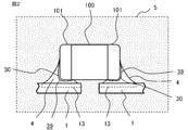
図1は本発明の実施の形態1によるパワー半導体装置の内部の概観模式図であり、図2は本発明の実施の形態1による応力緩和構造部を示す図である。本実施の形態1のパワー半導体装置50は、配線パターン状に成型された複数のリードフレーム1と、スイッチング可能なパワー半導体素子2と、パワー半導体素子2のスイッチングによる電圧変動を緩和させるセラミックコンデンサ(適宜、コンデンサとも称する)100と、チップ抵抗器(適宜、抵抗器とも称する)20などのチップ部品と、端子が形成される複数のリードフレーム1の間や、リードフレーム1とパワー半導体素子2との間を接続する配線部材3と、リードフレーム1、パワー半導体素子2、チップ部品等の実装部品、及び配線部材3を封止するモールド樹脂5とを備える。図1では、3つのパワー半導体素子2a、2b、2cが実装され、5つのパワー端子11a、11b、11c、11d、11eと3つの信号端子12a、12b、12cを備えるパワー半導体装置50の例を示した。なお、パワー半導体素子の符号は、総括的に2を用い、区別して説明する場合に2a、2b、2cを用いる。パワー端子の符号は、総括的に11を用い、区別して説明する場合に11a、11b、11c、11d、11eを用いる。信号端子の符号は、総括的に12を用い、区別して説明する場合に12a、12b、12cを用いる。
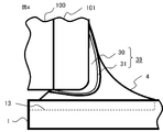
図6は、実施の形態2による応力緩和構造部を拡大した図である。実施の形態2のパワー半導体装置50における応力緩和構造部39は、コンデンサ100の外部電極101に接続する電極接続部37と外部電極101に接続しない電極非接続部38とを備える。外部電極101において、応力緩和構造部39の電極接続部37に接続する部分を第1電極部102とし、応力緩和構造部39の電極接続部37に接続しない部分を第2電極部103とする。図6において、第1電極部102は矢印区間102で示した部分であり、第2電極部103は矢印区間103で示した部分である。第2電極部103は、図6における外部電極101の上側、すなわち、はんだ4が接合した上限部(限界部)よりも上側ではなく、コンデンサ実装部13の側に形成される。
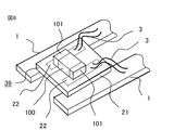
図7は、本発明の実施の形態3による応力緩和構造部を示す図である。実施の形態3のパワー半導体装置50は、コンデンサ100本体よりも剛性が低い金属板32からなる応力緩和構造部39を備える。金属板32の一端はコンデンサ100の外部電極101に接続され、金属板32の他の一端はリードフレーム1のコンデンサ実装部13に接続されている。この応力緩和構造部39は、コンデンサ100とリードフレーム1の間に金属板32が介在するように配置された構造なので、モールド工程の際にコンデンサ100に加わる成型圧、モールド時の型締め、パワー半導体装置50の動作時における温度サイクル等によるコンデンサ100に生じる応力を、金属板32が変形することにより緩和することができる。この結果、コンデンサ100に生じる応力に起因したコンデンサ不良を防止することができ、製造プロセスの歩留まりを向上できる。
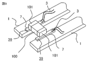
図8は、本発明の実施の形態4によるコンデンサ実装構造を示す図である。実施の形態4のパワー半導体装置50は、2つのリードフレーム1の間に固定された絶縁性の配線基板21上に形成された配線パターン22とコンデンサ100の外部電極101とが接合され、配線基板21に形成された配線パターン22とリードフレーム1とが別のワイヤーボンドなどの配線部材3により電気的に接続される構造を備える。すなわち、実施の形態4のパワー半導体装置50は、リードフレーム1及びコンデンサ100よりも剛性が低い配線基板21からなる応力緩和構造部39を備える。このように、実施の形態4のパワー半導体装置50は、コンデンサ100とリードフレーム1の間に配線基板21を配置することにより、モールド成型時の成型圧やモールド成型による型締めによる応力が、配線基板21により緩和されるので、直接コンデンサ100に生じることがなく、コンデンサ100が故障するのを防止することがきる。
Claims (11)
- モールド樹脂で封止されたパワー半導体装置であって、
配線パターン状に成型された複数のリードフレームと、
前記リードフレーム上に接合されたパワー半導体素子と、
互いに隣接した2つの前記リードフレームの間に配置されたコンデンサとを備え、
前記コンデンサは、当該コンデンサの外部電極が、当該コンデンサよりも剛性が低い応力緩和構造部を介して前記リードフレームに接続されたことを特徴とするパワー半導体装置。 - 前記コンデンサと前記リードフレームとの接続構造は、
当該コンデンサの外部電極に接続した前記応力緩和構造部と、前記応力緩和構造部と前記リードフレームを接続するはんだとを有し、
前記応力緩和構造部は、前記はんだよりも剛性が低いことを特徴とする請求項1記載のパワー半導体装置。 - 前記応力緩和構造部は、樹脂に導電性フィラーを配合した導電性応力緩和部を有することを特徴とする請求項1または2に記載のパワー半導体装置。
- 前記コンデンサは、当該コンデンサの前記外部電極における前記リードフレームに対向する側において、前記応力緩和構造部が接続されない非接続部を有し、
前記非接続部は前記モールド樹脂により覆われたことを特徴とする請求項1乃至3のいずれか1項に記載のパワー半導体装置。 - 前記応力緩和構造部は、前記コンデンサの前記外部電極に接続する電極接続部と、前記外部電極に接続しない電極非接続部とを有することを特徴とする請求項1乃至4のいずれか1項に記載のパワー半導体装置。
- 前記応力緩和構造部は、金属板であることを特徴とする請求項1または2に記載のパワー半導体装置。
- 前記応力緩和構造部は、前記コンデンサの前記外部電極に接続する配線パターンを有する絶縁性の配線基板であることを特徴とする請求項1または2に記載のパワー半導体装置。
- 前記応力緩和構造部は、前記リードフレーム上に配置されると共に当該リードフレームと絶縁された第2のリードフレームであり、
前記第2のリードフレームは、前記コンデンサの前記外部電極に接続されると共に、配線部材により前記リードフレームに接続されたことを特徴とする請求項1または2に記載のパワー半導体装置。 - 請求項1乃至8のいずれか1項に記載のパワー半導体装置は、車載用の回転電機に設置され、前記回転電機の電機子に電流を供給することを特徴とするパワー半導体装置。
- 前記パワー半導体素子は、ワイドバンドギャップ半導体材料により形成されていることを特徴とする請求項1乃至9のいずれか1項に記載のパワー半導体装置。
- 前記ワイドバンドギャップ半導体材料は、炭化珪素、窒化ガリウム系材料、またはダイヤモンドのうちいずれかであることを特徴とする請求項10記載のパワー半導体装置。
Priority Applications (5)
| Application Number | Priority Date | Filing Date | Title |
|---|---|---|---|
| EP12884280.4A EP2894952B1 (en) | 2012-09-07 | 2012-09-07 | Power semiconductor device |
| JP2014534126A JP5989124B2 (ja) | 2012-09-07 | 2012-09-07 | パワー半導体装置 |
| PCT/JP2012/072908 WO2014038066A1 (ja) | 2012-09-07 | 2012-09-07 | パワー半導体装置 |
| CN201280075682.1A CN104604344B (zh) | 2012-09-07 | 2012-09-07 | 功率半导体装置 |
| US14/402,538 US9620444B2 (en) | 2012-09-07 | 2012-09-07 | Power semiconductor device |
Applications Claiming Priority (1)
| Application Number | Priority Date | Filing Date | Title |
|---|---|---|---|
| PCT/JP2012/072908 WO2014038066A1 (ja) | 2012-09-07 | 2012-09-07 | パワー半導体装置 |
Publications (1)
| Publication Number | Publication Date |
|---|---|
| WO2014038066A1 true WO2014038066A1 (ja) | 2014-03-13 |
Family
ID=50236714
Family Applications (1)
| Application Number | Title | Priority Date | Filing Date |
|---|---|---|---|
| PCT/JP2012/072908 WO2014038066A1 (ja) | 2012-09-07 | 2012-09-07 | パワー半導体装置 |
Country Status (5)
| Country | Link |
|---|---|
| US (1) | US9620444B2 (ja) |
| EP (1) | EP2894952B1 (ja) |
| JP (1) | JP5989124B2 (ja) |
| CN (1) | CN104604344B (ja) |
| WO (1) | WO2014038066A1 (ja) |
Cited By (15)
| Publication number | Priority date | Publication date | Assignee | Title |
|---|---|---|---|---|
| EP3012861A1 (de) * | 2014-10-21 | 2016-04-27 | Robert Bosch Gmbh | Schaltungsanordnung und leistungsmodul |
| JP2017203709A (ja) * | 2016-05-12 | 2017-11-16 | 株式会社東海理化電機製作所 | モジュール及びその製造方法 |
| JP2018032670A (ja) * | 2016-08-22 | 2018-03-01 | Koa株式会社 | チップ部品、チップ部品の実装構造、チップ抵抗器の製造方法 |
| JP2018049999A (ja) * | 2016-09-23 | 2018-03-29 | Tdk株式会社 | 電子部品及び電子部品装置 |
| JP2019047092A (ja) * | 2017-09-07 | 2019-03-22 | Tdk株式会社 | 電子部品 |
| JP2019047091A (ja) * | 2017-09-07 | 2019-03-22 | Tdk株式会社 | 電子部品 |
| JP2019050278A (ja) * | 2017-09-08 | 2019-03-28 | Tdk株式会社 | 電子部品及び電子部品装置 |
| JP2019067787A (ja) * | 2017-09-28 | 2019-04-25 | Tdk株式会社 | 電子部品 |
| JP2019083254A (ja) * | 2017-10-30 | 2019-05-30 | Tdk株式会社 | 電子部品 |
| JP2019083252A (ja) * | 2017-10-30 | 2019-05-30 | Tdk株式会社 | 電子部品 |
| JP2019083253A (ja) * | 2017-10-30 | 2019-05-30 | Tdk株式会社 | 電子部品及び電子部品装置 |
| JPWO2019132017A1 (ja) * | 2017-12-29 | 2020-12-17 | 株式会社村田製作所 | 積層セラミックコンデンサ、積層セラミックコンデンサの実装構造体および電子部品連 |
| JPWO2021019867A1 (ja) * | 2019-07-30 | 2021-02-04 | ||
| CN112863874A (zh) * | 2016-09-23 | 2021-05-28 | Tdk株式会社 | 电子部件和电子部件装置 |
| WO2022004332A1 (ja) * | 2020-07-01 | 2022-01-06 | 株式会社オートネットワーク技術研究所 | 回路構成体 |
Families Citing this family (8)
| Publication number | Priority date | Publication date | Assignee | Title |
|---|---|---|---|---|
| US9949378B2 (en) | 2014-04-14 | 2018-04-17 | Presidio Components, Inc. | Electrical devices with solder dam |
| US9647363B2 (en) * | 2014-09-19 | 2017-05-09 | Intel Corporation | Techniques and configurations to control movement and position of surface mounted electrical devices |
| KR102029493B1 (ko) * | 2014-09-29 | 2019-10-07 | 삼성전기주식회사 | 적층 세라믹 커패시터 및 그 실장 기판 |
| US10074590B1 (en) * | 2017-07-02 | 2018-09-11 | Infineon Technologies Ag | Molded package with chip carrier comprising brazed electrically conductive layers |
| DE112019002333T5 (de) * | 2018-05-09 | 2021-01-21 | Mitsubishi Electric Corporation | Leistungshalbleitermodul, Verfahren zum Herstellen desselben und Leistungswandlungsvorrichtung |
| FR3092453A1 (fr) | 2019-01-31 | 2020-08-07 | Valeo Equipements Electriques Moteur | Module électronique de puissance, convertisseur de tension et système électrique |
| CN112448561B (zh) * | 2019-08-30 | 2022-04-15 | 台达电子企业管理(上海)有限公司 | 电源模块及电源模块的制备方法 |
| US11495549B2 (en) | 2021-02-25 | 2022-11-08 | Texas Instruments Incorporated | Electronic device with crack arrest structure |
Citations (8)
| Publication number | Priority date | Publication date | Assignee | Title |
|---|---|---|---|---|
| JPS5972757A (ja) | 1982-10-20 | 1984-04-24 | Fujitsu Ltd | 半導体装置 |
| JPH11238963A (ja) * | 1998-02-21 | 1999-08-31 | Mitsui High Tec Inc | 電子部品の面実装方法及びその実装構造体 |
| JP2002076605A (ja) * | 2000-06-12 | 2002-03-15 | Hitachi Ltd | 半導体モジュール及び半導体装置を接続した回路基板 |
| JP2004031768A (ja) * | 2002-06-27 | 2004-01-29 | Denso Corp | 電子装置の実装方法 |
| JP2006324629A (ja) * | 2005-04-21 | 2006-11-30 | Denso Corp | 電子部品の実装構造およびその実装方法 |
| JP2009032865A (ja) * | 2007-07-26 | 2009-02-12 | Hitachi Ltd | 電子装置及び電子装置の製造方法 |
| JP2011003818A (ja) * | 2009-06-22 | 2011-01-06 | Denso Corp | モールドパッケージ |
| JP2012164796A (ja) * | 2011-02-07 | 2012-08-30 | Mitsubishi Electric Corp | パワー半導体装置 |
Family Cites Families (29)
| Publication number | Priority date | Publication date | Assignee | Title |
|---|---|---|---|---|
| JPH01276655A (ja) * | 1988-04-27 | 1989-11-07 | Japan Radio Co Ltd | トランスファーモールド型集積回路 |
| JPH03220712A (ja) * | 1990-01-25 | 1991-09-27 | Nec Corp | ワイヤボンディング構造体 |
| JPH06232332A (ja) * | 1993-02-08 | 1994-08-19 | Hitachi Ltd | 半導体装置 |
| JPH08203771A (ja) * | 1995-01-27 | 1996-08-09 | Murata Mfg Co Ltd | セラミック電子部品 |
| JPH0936298A (ja) * | 1995-07-25 | 1997-02-07 | Denso Corp | リードフレーム |
| JP2000133909A (ja) | 1998-10-22 | 2000-05-12 | Matsushita Electric Ind Co Ltd | チップコンデンサのプリント配線基板実装構造 |
| JP3376970B2 (ja) * | 1999-09-08 | 2003-02-17 | 株式会社村田製作所 | セラミック電子部品 |
| JP3376971B2 (ja) * | 1999-09-09 | 2003-02-17 | 株式会社村田製作所 | セラミック電子部品 |
| KR100398716B1 (ko) | 2000-06-12 | 2003-09-19 | 가부시키가이샤 히타치세이사쿠쇼 | 반도체 모듈 및 반도체 장치를 접속한 회로 기판 |
| JP2002057064A (ja) * | 2000-08-11 | 2002-02-22 | Murata Mfg Co Ltd | 積層セラミック電子部品 |
| JP2002232110A (ja) | 2001-02-02 | 2002-08-16 | Tohoku Pioneer Corp | 積層セラミックコンデンサを実装した回路基板 |
| JP4923367B2 (ja) * | 2001-09-13 | 2012-04-25 | 株式会社デンソー | 電気素子の実装構造 |
| JP2003243595A (ja) | 2002-02-19 | 2003-08-29 | New Japan Radio Co Ltd | 受動部品内蔵型半導体装置 |
| JP4296472B2 (ja) | 2002-10-31 | 2009-07-15 | ソニー株式会社 | 情報処理装置及び電源回路 |
| JP2004179568A (ja) | 2002-11-29 | 2004-06-24 | Kyocera Corp | 積層セラミック部品の製造方法 |
| JP2004296936A (ja) * | 2003-03-27 | 2004-10-21 | Kyocera Corp | セラミック電子部品 |
| JP2006032774A (ja) * | 2004-07-20 | 2006-02-02 | Denso Corp | 電子装置 |
| US6917510B1 (en) * | 2004-10-27 | 2005-07-12 | Kemet Corporation | Extended terminal ceramic SMD |
| JP4046120B2 (ja) | 2005-01-27 | 2008-02-13 | 三菱電機株式会社 | 絶縁シートの製造方法およびパワーモジュールの製造方法 |
| JP4640214B2 (ja) * | 2006-02-28 | 2011-03-02 | 株式会社デンソー | 電子部品の接続構造 |
| JP4998467B2 (ja) | 2006-06-28 | 2012-08-15 | 株式会社村田製作所 | セラミック電子部品およびその製造方法 |
| JP4803451B2 (ja) * | 2006-12-26 | 2011-10-26 | Tdk株式会社 | 電子部品及びその実装構造 |
| JP2009059888A (ja) * | 2007-08-31 | 2009-03-19 | Murata Mfg Co Ltd | 積層セラミックコンデンサ |
| JP5163069B2 (ja) * | 2007-11-20 | 2013-03-13 | 株式会社デンソー | 半導体装置 |
| JP2009238923A (ja) | 2008-03-26 | 2009-10-15 | Toyota Industries Corp | 電子機器 |
| JP5099243B2 (ja) * | 2010-04-14 | 2012-12-19 | 株式会社デンソー | 半導体モジュール |
| US9819297B2 (en) * | 2010-09-15 | 2017-11-14 | Mitsubishi Electric Corporation | Power conversion device, motor including the same, air conditioner having the motor incorporated therein, and ventilation fan having the motor incorporated therein |
| JP5162685B2 (ja) | 2011-02-17 | 2013-03-13 | 三菱電機株式会社 | Dc/dc電圧変換装置 |
| WO2012114818A1 (ja) * | 2011-02-23 | 2012-08-30 | 株式会社村田製作所 | セラミック電子部品、及びセラミック電子部品の設計方法 |
-
2012
- 2012-09-07 EP EP12884280.4A patent/EP2894952B1/en active Active
- 2012-09-07 JP JP2014534126A patent/JP5989124B2/ja active Active
- 2012-09-07 US US14/402,538 patent/US9620444B2/en active Active
- 2012-09-07 CN CN201280075682.1A patent/CN104604344B/zh active Active
- 2012-09-07 WO PCT/JP2012/072908 patent/WO2014038066A1/ja active Application Filing
Patent Citations (8)
| Publication number | Priority date | Publication date | Assignee | Title |
|---|---|---|---|---|
| JPS5972757A (ja) | 1982-10-20 | 1984-04-24 | Fujitsu Ltd | 半導体装置 |
| JPH11238963A (ja) * | 1998-02-21 | 1999-08-31 | Mitsui High Tec Inc | 電子部品の面実装方法及びその実装構造体 |
| JP2002076605A (ja) * | 2000-06-12 | 2002-03-15 | Hitachi Ltd | 半導体モジュール及び半導体装置を接続した回路基板 |
| JP2004031768A (ja) * | 2002-06-27 | 2004-01-29 | Denso Corp | 電子装置の実装方法 |
| JP2006324629A (ja) * | 2005-04-21 | 2006-11-30 | Denso Corp | 電子部品の実装構造およびその実装方法 |
| JP2009032865A (ja) * | 2007-07-26 | 2009-02-12 | Hitachi Ltd | 電子装置及び電子装置の製造方法 |
| JP2011003818A (ja) * | 2009-06-22 | 2011-01-06 | Denso Corp | モールドパッケージ |
| JP2012164796A (ja) * | 2011-02-07 | 2012-08-30 | Mitsubishi Electric Corp | パワー半導体装置 |
Non-Patent Citations (1)
| Title |
|---|
| See also references of EP2894952A1 |
Cited By (22)
| Publication number | Priority date | Publication date | Assignee | Title |
|---|---|---|---|---|
| EP3012861A1 (de) * | 2014-10-21 | 2016-04-27 | Robert Bosch Gmbh | Schaltungsanordnung und leistungsmodul |
| JP2017203709A (ja) * | 2016-05-12 | 2017-11-16 | 株式会社東海理化電機製作所 | モジュール及びその製造方法 |
| JP2018032670A (ja) * | 2016-08-22 | 2018-03-01 | Koa株式会社 | チップ部品、チップ部品の実装構造、チップ抵抗器の製造方法 |
| CN112863874A (zh) * | 2016-09-23 | 2021-05-28 | Tdk株式会社 | 电子部件和电子部件装置 |
| JP2018049999A (ja) * | 2016-09-23 | 2018-03-29 | Tdk株式会社 | 電子部品及び電子部品装置 |
| US11763996B2 (en) | 2016-09-23 | 2023-09-19 | Tdk Corporation | Electronic component and electronic component device |
| US11594378B2 (en) | 2016-09-23 | 2023-02-28 | Tdk Corporation | Electronic component and electronic component device |
| CN112863874B (zh) * | 2016-09-23 | 2023-02-03 | Tdk株式会社 | 电子部件和电子部件装置 |
| US11264172B2 (en) | 2016-09-23 | 2022-03-01 | Tdk Corporation | Electronic component and electronic component device |
| JP2019047092A (ja) * | 2017-09-07 | 2019-03-22 | Tdk株式会社 | 電子部品 |
| JP2019047091A (ja) * | 2017-09-07 | 2019-03-22 | Tdk株式会社 | 電子部品 |
| JP2019050278A (ja) * | 2017-09-08 | 2019-03-28 | Tdk株式会社 | 電子部品及び電子部品装置 |
| JP7003541B2 (ja) | 2017-09-28 | 2022-01-20 | Tdk株式会社 | 電子部品及び電子部品装置 |
| JP2019067787A (ja) * | 2017-09-28 | 2019-04-25 | Tdk株式会社 | 電子部品 |
| JP2019083253A (ja) * | 2017-10-30 | 2019-05-30 | Tdk株式会社 | 電子部品及び電子部品装置 |
| JP2019083252A (ja) * | 2017-10-30 | 2019-05-30 | Tdk株式会社 | 電子部品 |
| JP2019083254A (ja) * | 2017-10-30 | 2019-05-30 | Tdk株式会社 | 電子部品 |
| JPWO2019132017A1 (ja) * | 2017-12-29 | 2020-12-17 | 株式会社村田製作所 | 積層セラミックコンデンサ、積層セラミックコンデンサの実装構造体および電子部品連 |
| JP7040534B2 (ja) | 2017-12-29 | 2022-03-23 | 株式会社村田製作所 | 積層セラミックコンデンサ、積層セラミックコンデンサの実装構造体および電子部品連 |
| JPWO2021019867A1 (ja) * | 2019-07-30 | 2021-02-04 | ||
| JP7166464B2 (ja) | 2019-07-30 | 2022-11-07 | 三菱電機株式会社 | チップ部品、チップ部品の製造方法、および電子機器の製造方法 |
| WO2022004332A1 (ja) * | 2020-07-01 | 2022-01-06 | 株式会社オートネットワーク技術研究所 | 回路構成体 |
Also Published As
| Publication number | Publication date |
|---|---|
| EP2894952A1 (en) | 2015-07-15 |
| CN104604344A (zh) | 2015-05-06 |
| US20150287670A1 (en) | 2015-10-08 |
| JPWO2014038066A1 (ja) | 2016-08-08 |
| EP2894952A4 (en) | 2017-01-25 |
| JP5989124B2 (ja) | 2016-09-07 |
| EP2894952B1 (en) | 2018-06-06 |
| US9620444B2 (en) | 2017-04-11 |
| CN104604344B (zh) | 2019-04-16 |
Similar Documents
| Publication | Publication Date | Title |
|---|---|---|
| JP5989124B2 (ja) | パワー半導体装置 | |
| US9171773B2 (en) | Semiconductor device | |
| TW498550B (en) | Semiconductor device | |
| US9572291B2 (en) | Semiconductor device and method for manufacturing same | |
| CN109727960B (zh) | 半导体模块、其制造方法以及电力变换装置 | |
| WO2015174158A1 (ja) | パワー半導体モジュールおよび複合モジュール | |
| JP4947135B2 (ja) | 半導体パッケージおよびその製造方法 | |
| JP2016197677A (ja) | パワー半導体装置および車載用回転電機の駆動装置 | |
| US10615131B2 (en) | Semiconductor device with high quality and reliability wiring connection, and method for manufacturing the same | |
| CN107818963B (zh) | 半导体装置及半导体装置的制造方法 | |
| US20230215788A1 (en) | Power module and manufacturing method thereof, converter, and electronic device | |
| JP2005150209A (ja) | 電子装置およびその製造方法 | |
| JP6952889B2 (ja) | パワー半導体モジュール及びその製造方法並びに電力変換装置 | |
| CN111276448A (zh) | 半导体装置及电力转换装置 | |
| JP2013157398A (ja) | 半導体装置およびその製造方法 | |
| CN108735614B (zh) | 半导体装置及半导体装置的制造方法 | |
| JP4861200B2 (ja) | パワーモジュール | |
| JP2004048084A (ja) | 半導体パワーモジュール | |
| JP2013135161A (ja) | 半導体装置およびその製造方法 | |
| KR102371636B1 (ko) | 양면 기판 반도체 제조 방법 | |
| US20230343661A1 (en) | Semiconductor Encapsulant Strength Enhancer | |
| WO2013157172A1 (ja) | 半導体パッケージ及びその製造方法、半導体モジュール、並びに半導体装置 | |
| WO2023175861A1 (ja) | 半導体装置 | |
| JP2021141237A (ja) | 半導体装置 | |
| WO2017086248A1 (ja) | 電力用半導体装置および電力用半導体装置の製造方法 |
Legal Events
| Date | Code | Title | Description |
|---|---|---|---|
| 121 | Ep: the epo has been informed by wipo that ep was designated in this application |
Ref document number: 12884280 Country of ref document: EP Kind code of ref document: A1 |
|
| ENP | Entry into the national phase |
Ref document number: 2014534126 Country of ref document: JP Kind code of ref document: A |
|
| WWE | Wipo information: entry into national phase |
Ref document number: 14402538 Country of ref document: US |
|
| WWE | Wipo information: entry into national phase |
Ref document number: 2012884280 Country of ref document: EP |
|
| NENP | Non-entry into the national phase |
Ref country code: DE |