WO2013108657A1 - Procédé de fabrication pour dispositif à semi-conducteur - Google Patents
Procédé de fabrication pour dispositif à semi-conducteur Download PDFInfo
- Publication number
- WO2013108657A1 WO2013108657A1 PCT/JP2013/050093 JP2013050093W WO2013108657A1 WO 2013108657 A1 WO2013108657 A1 WO 2013108657A1 JP 2013050093 W JP2013050093 W JP 2013050093W WO 2013108657 A1 WO2013108657 A1 WO 2013108657A1
- Authority
- WO
- WIPO (PCT)
- Prior art keywords
- substrate
- semiconductor substrate
- manufacturing
- semiconductor device
- protective film
- Prior art date
Links
- 239000004065 semiconductor Substances 0.000 title claims description 209
- 238000004519 manufacturing process Methods 0.000 title claims description 65
- 239000000758 substrate Substances 0.000 claims abstract description 329
- 230000001681 protective effect Effects 0.000 claims abstract description 56
- 238000000034 method Methods 0.000 claims description 94
- 239000000126 substance Substances 0.000 claims description 28
- 230000015572 biosynthetic process Effects 0.000 claims description 14
- 238000000227 grinding Methods 0.000 claims description 11
- 239000000463 material Substances 0.000 claims description 7
- 238000004140 cleaning Methods 0.000 claims description 4
- 239000010410 layer Substances 0.000 description 63
- 238000003384 imaging method Methods 0.000 description 35
- 230000008569 process Effects 0.000 description 33
- 238000012545 processing Methods 0.000 description 25
- 239000002184 metal Substances 0.000 description 11
- 229910052751 metal Inorganic materials 0.000 description 11
- 239000000243 solution Substances 0.000 description 11
- 238000011109 contamination Methods 0.000 description 9
- 239000000428 dust Substances 0.000 description 9
- 238000010828 elution Methods 0.000 description 9
- 238000010586 diagram Methods 0.000 description 8
- 230000006870 function Effects 0.000 description 8
- 238000006243 chemical reaction Methods 0.000 description 5
- 238000009966 trimming Methods 0.000 description 5
- 239000011248 coating agent Substances 0.000 description 4
- 238000000576 coating method Methods 0.000 description 4
- 238000012546 transfer Methods 0.000 description 4
- 239000002253 acid Substances 0.000 description 3
- 239000012790 adhesive layer Substances 0.000 description 3
- 239000004020 conductor Substances 0.000 description 3
- 238000012937 correction Methods 0.000 description 3
- 239000012634 fragment Substances 0.000 description 3
- 238000012986 modification Methods 0.000 description 3
- 230000004048 modification Effects 0.000 description 3
- 230000002093 peripheral effect Effects 0.000 description 3
- 238000001039 wet etching Methods 0.000 description 3
- 229910004298 SiO 2 Inorganic materials 0.000 description 2
- 230000003321 amplification Effects 0.000 description 2
- 238000000137 annealing Methods 0.000 description 2
- 238000000231 atomic layer deposition Methods 0.000 description 2
- 238000005229 chemical vapour deposition Methods 0.000 description 2
- 238000000151 deposition Methods 0.000 description 2
- 230000008021 deposition Effects 0.000 description 2
- 238000009792 diffusion process Methods 0.000 description 2
- 238000005530 etching Methods 0.000 description 2
- 238000007667 floating Methods 0.000 description 2
- 238000005286 illumination Methods 0.000 description 2
- 230000010354 integration Effects 0.000 description 2
- 239000007788 liquid Substances 0.000 description 2
- 238000005259 measurement Methods 0.000 description 2
- 238000003199 nucleic acid amplification method Methods 0.000 description 2
- RYGMFSIKBFXOCR-UHFFFAOYSA-N Copper Chemical compound [Cu] RYGMFSIKBFXOCR-UHFFFAOYSA-N 0.000 description 1
- GRYLNZFGIOXLOG-UHFFFAOYSA-N Nitric acid Chemical compound O[N+]([O-])=O GRYLNZFGIOXLOG-UHFFFAOYSA-N 0.000 description 1
- XUIMIQQOPSSXEZ-UHFFFAOYSA-N Silicon Chemical compound [Si] XUIMIQQOPSSXEZ-UHFFFAOYSA-N 0.000 description 1
- 230000002411 adverse Effects 0.000 description 1
- 230000003139 buffering effect Effects 0.000 description 1
- 238000012993 chemical processing Methods 0.000 description 1
- 229910052802 copper Inorganic materials 0.000 description 1
- 239000010949 copper Substances 0.000 description 1
- 238000013461 design Methods 0.000 description 1
- 238000001514 detection method Methods 0.000 description 1
- 238000007688 edging Methods 0.000 description 1
- 230000000694 effects Effects 0.000 description 1
- 238000005401 electroluminescence Methods 0.000 description 1
- 230000004907 flux Effects 0.000 description 1
- 239000007789 gas Substances 0.000 description 1
- LMRFGCUCLQUNCZ-UHFFFAOYSA-N hydrogen peroxide hydrofluoride Chemical compound F.OO LMRFGCUCLQUNCZ-UHFFFAOYSA-N 0.000 description 1
- 230000006872 improvement Effects 0.000 description 1
- 239000012535 impurity Substances 0.000 description 1
- 238000010884 ion-beam technique Methods 0.000 description 1
- 238000005304 joining Methods 0.000 description 1
- 238000003475 lamination Methods 0.000 description 1
- 239000004973 liquid crystal related substance Substances 0.000 description 1
- 238000003754 machining Methods 0.000 description 1
- 239000011159 matrix material Substances 0.000 description 1
- 239000008155 medical solution Substances 0.000 description 1
- 239000011259 mixed solution Substances 0.000 description 1
- 229910017604 nitric acid Inorganic materials 0.000 description 1
- 150000004767 nitrides Chemical class 0.000 description 1
- 230000003287 optical effect Effects 0.000 description 1
- 239000002245 particle Substances 0.000 description 1
- 229920002120 photoresistant polymer Polymers 0.000 description 1
- 238000009832 plasma treatment Methods 0.000 description 1
- 238000007517 polishing process Methods 0.000 description 1
- 230000001902 propagating effect Effects 0.000 description 1
- 230000004044 response Effects 0.000 description 1
- 229910052710 silicon Inorganic materials 0.000 description 1
- 239000010703 silicon Substances 0.000 description 1
- 229910052814 silicon oxide Inorganic materials 0.000 description 1
- 238000010129 solution processing Methods 0.000 description 1
- 238000005507 spraying Methods 0.000 description 1
- XLYOFNOQVPJJNP-UHFFFAOYSA-N water Substances O XLYOFNOQVPJJNP-UHFFFAOYSA-N 0.000 description 1
Images


Classifications
-
- H—ELECTRICITY
- H01—ELECTRIC ELEMENTS
- H01L—SEMICONDUCTOR DEVICES NOT COVERED BY CLASS H10
- H01L27/00—Devices consisting of a plurality of semiconductor or other solid-state components formed in or on a common substrate
- H01L27/14—Devices consisting of a plurality of semiconductor or other solid-state components formed in or on a common substrate including semiconductor components sensitive to infrared radiation, light, electromagnetic radiation of shorter wavelength or corpuscular radiation and specially adapted either for the conversion of the energy of such radiation into electrical energy or for the control of electrical energy by such radiation
- H01L27/144—Devices controlled by radiation
- H01L27/146—Imager structures
- H01L27/14683—Processes or apparatus peculiar to the manufacture or treatment of these devices or parts thereof
- H01L27/14687—Wafer level processing
-
- H—ELECTRICITY
- H01—ELECTRIC ELEMENTS
- H01L—SEMICONDUCTOR DEVICES NOT COVERED BY CLASS H10
- H01L25/00—Assemblies consisting of a plurality of individual semiconductor or other solid state devices ; Multistep manufacturing processes thereof
- H01L25/50—Multistep manufacturing processes of assemblies consisting of devices, each device being of a type provided for in group H01L27/00 or H01L29/00
-
- H—ELECTRICITY
- H01—ELECTRIC ELEMENTS
- H01L—SEMICONDUCTOR DEVICES NOT COVERED BY CLASS H10
- H01L27/00—Devices consisting of a plurality of semiconductor or other solid-state components formed in or on a common substrate
- H01L27/14—Devices consisting of a plurality of semiconductor or other solid-state components formed in or on a common substrate including semiconductor components sensitive to infrared radiation, light, electromagnetic radiation of shorter wavelength or corpuscular radiation and specially adapted either for the conversion of the energy of such radiation into electrical energy or for the control of electrical energy by such radiation
- H01L27/144—Devices controlled by radiation
- H01L27/146—Imager structures
- H01L27/14601—Structural or functional details thereof
- H01L27/14634—Assemblies, i.e. Hybrid structures
-
- H—ELECTRICITY
- H01—ELECTRIC ELEMENTS
- H01L—SEMICONDUCTOR DEVICES NOT COVERED BY CLASS H10
- H01L27/00—Devices consisting of a plurality of semiconductor or other solid-state components formed in or on a common substrate
- H01L27/14—Devices consisting of a plurality of semiconductor or other solid-state components formed in or on a common substrate including semiconductor components sensitive to infrared radiation, light, electromagnetic radiation of shorter wavelength or corpuscular radiation and specially adapted either for the conversion of the energy of such radiation into electrical energy or for the control of electrical energy by such radiation
- H01L27/144—Devices controlled by radiation
- H01L27/146—Imager structures
- H01L27/14601—Structural or functional details thereof
- H01L27/1464—Back illuminated imager structures
-
- H—ELECTRICITY
- H01—ELECTRIC ELEMENTS
- H01L—SEMICONDUCTOR DEVICES NOT COVERED BY CLASS H10
- H01L27/00—Devices consisting of a plurality of semiconductor or other solid-state components formed in or on a common substrate
- H01L27/14—Devices consisting of a plurality of semiconductor or other solid-state components formed in or on a common substrate including semiconductor components sensitive to infrared radiation, light, electromagnetic radiation of shorter wavelength or corpuscular radiation and specially adapted either for the conversion of the energy of such radiation into electrical energy or for the control of electrical energy by such radiation
- H01L27/144—Devices controlled by radiation
- H01L27/146—Imager structures
- H01L27/14683—Processes or apparatus peculiar to the manufacture or treatment of these devices or parts thereof
- H01L27/14689—MOS based technologies
-
- H—ELECTRICITY
- H01—ELECTRIC ELEMENTS
- H01L—SEMICONDUCTOR DEVICES NOT COVERED BY CLASS H10
- H01L27/00—Devices consisting of a plurality of semiconductor or other solid-state components formed in or on a common substrate
- H01L27/14—Devices consisting of a plurality of semiconductor or other solid-state components formed in or on a common substrate including semiconductor components sensitive to infrared radiation, light, electromagnetic radiation of shorter wavelength or corpuscular radiation and specially adapted either for the conversion of the energy of such radiation into electrical energy or for the control of electrical energy by such radiation
- H01L27/144—Devices controlled by radiation
- H01L27/146—Imager structures
- H01L27/14683—Processes or apparatus peculiar to the manufacture or treatment of these devices or parts thereof
- H01L27/1469—Assemblies, i.e. hybrid integration
-
- H—ELECTRICITY
- H01—ELECTRIC ELEMENTS
- H01L—SEMICONDUCTOR DEVICES NOT COVERED BY CLASS H10
- H01L31/00—Semiconductor devices sensitive to infrared radiation, light, electromagnetic radiation of shorter wavelength or corpuscular radiation and specially adapted either for the conversion of the energy of such radiation into electrical energy or for the control of electrical energy by such radiation; Processes or apparatus specially adapted for the manufacture or treatment thereof or of parts thereof; Details thereof
- H01L31/18—Processes or apparatus specially adapted for the manufacture or treatment of these devices or of parts thereof
- H01L31/1876—Particular processes or apparatus for batch treatment of the devices
-
- H—ELECTRICITY
- H01—ELECTRIC ELEMENTS
- H01L—SEMICONDUCTOR DEVICES NOT COVERED BY CLASS H10
- H01L25/00—Assemblies consisting of a plurality of individual semiconductor or other solid state devices ; Multistep manufacturing processes thereof
- H01L25/03—Assemblies consisting of a plurality of individual semiconductor or other solid state devices ; Multistep manufacturing processes thereof all the devices being of a type provided for in the same subgroup of groups H01L27/00 - H01L33/00, or in a single subclass of H10K, H10N, e.g. assemblies of rectifier diodes
- H01L25/04—Assemblies consisting of a plurality of individual semiconductor or other solid state devices ; Multistep manufacturing processes thereof all the devices being of a type provided for in the same subgroup of groups H01L27/00 - H01L33/00, or in a single subclass of H10K, H10N, e.g. assemblies of rectifier diodes the devices not having separate containers
- H01L25/065—Assemblies consisting of a plurality of individual semiconductor or other solid state devices ; Multistep manufacturing processes thereof all the devices being of a type provided for in the same subgroup of groups H01L27/00 - H01L33/00, or in a single subclass of H10K, H10N, e.g. assemblies of rectifier diodes the devices not having separate containers the devices being of a type provided for in group H01L27/00
- H01L25/0657—Stacked arrangements of devices
-
- H—ELECTRICITY
- H01—ELECTRIC ELEMENTS
- H01L—SEMICONDUCTOR DEVICES NOT COVERED BY CLASS H10
- H01L2924/00—Indexing scheme for arrangements or methods for connecting or disconnecting semiconductor or solid-state bodies as covered by H01L24/00
- H01L2924/0001—Technical content checked by a classifier
- H01L2924/0002—Not covered by any one of groups H01L24/00, H01L24/00 and H01L2224/00
-
- Y—GENERAL TAGGING OF NEW TECHNOLOGICAL DEVELOPMENTS; GENERAL TAGGING OF CROSS-SECTIONAL TECHNOLOGIES SPANNING OVER SEVERAL SECTIONS OF THE IPC; TECHNICAL SUBJECTS COVERED BY FORMER USPC CROSS-REFERENCE ART COLLECTIONS [XRACs] AND DIGESTS
- Y02—TECHNOLOGIES OR APPLICATIONS FOR MITIGATION OR ADAPTATION AGAINST CLIMATE CHANGE
- Y02E—REDUCTION OF GREENHOUSE GAS [GHG] EMISSIONS, RELATED TO ENERGY GENERATION, TRANSMISSION OR DISTRIBUTION
- Y02E10/00—Energy generation through renewable energy sources
- Y02E10/50—Photovoltaic [PV] energy
-
- Y—GENERAL TAGGING OF NEW TECHNOLOGICAL DEVELOPMENTS; GENERAL TAGGING OF CROSS-SECTIONAL TECHNOLOGIES SPANNING OVER SEVERAL SECTIONS OF THE IPC; TECHNICAL SUBJECTS COVERED BY FORMER USPC CROSS-REFERENCE ART COLLECTIONS [XRACs] AND DIGESTS
- Y02—TECHNOLOGIES OR APPLICATIONS FOR MITIGATION OR ADAPTATION AGAINST CLIMATE CHANGE
- Y02P—CLIMATE CHANGE MITIGATION TECHNOLOGIES IN THE PRODUCTION OR PROCESSING OF GOODS
- Y02P70/00—Climate change mitigation technologies in the production process for final industrial or consumer products
- Y02P70/50—Manufacturing or production processes characterised by the final manufactured product
Definitions
- the present disclosure relates to a method of manufacturing a semiconductor device having a bonding structure of a plurality of substrates.
- the upper substrate is thinned to a desired thickness by a grinding process.
- devices having various functions for example, memory devices, logic devices, image sensor devices
- the upper substrate is thinned to a desired thickness by a grinding process.
- a first method for manufacturing a semiconductor device includes the following (A1) to (C1).
- A1) The first substrate having the first element and the second substrate having the second element are bonded so that the element formation surfaces face each other.
- B1) At least at the end of the second substrate having the second element.
- Forming a protective film C1) Thinning the first substrate
- the upper layer substrate (second substrate) is thinned after forming a protective film on the end portion of the lower layer substrate (first substrate). This reduces the occurrence of damage to the lower substrate when the upper substrate is thinned.
- the second method for manufacturing a semiconductor device includes the following (A2) to (D2). (A2) Forming a thin portion at the end of the first substrate having the first element (B2) Forming a protective film that does not absorb the laser at least at the end of the second substrate having the second element (C2) The second element and the first element are made to face each other, and the second substrate and the first substrate are bonded together (D2). The thin portion of the first substrate is selectively removed by a laser.
- a protective film that does not absorb a laser is formed on an end portion of a lower layer substrate (second substrate), and an end portion of an upper layer substrate (first substrate) is formed. Forms a thin part and removes the end of the upper substrate. This reduces the occurrence of damage to the lower substrate when the end portion of the upper substrate is removed.
- a third method for manufacturing a semiconductor device includes the following (A3) to (C3).
- A3) A first substrate having a first element and a second substrate having a second element are bonded to each other with the first element and the second element facing each other.
- B3) The inside excluding the end of the first substrate Thin the region (C3) Remove the edge of the first substrate
- the inner region excluding the end portion of the upper layer substrate is thinned, and then the end portion of the upper layer substrate Remove. This reduces the occurrence of damage to the lower substrate when the end portion of the upper substrate is removed.
- the upper layer substrate is thinned after forming the protective film on the end portion of the lower layer substrate, the upper layer substrate is not damaged. It is possible to reduce the thickness of the substrate.
- the protective film that does not absorb the laser is provided at the end of the lower substrate, and the thin portion is provided at the end of the upper substrate. It is possible to remove the end portion of the upper layer substrate without damaging the substrate.
- the end portion of the upper layer substrate is removed. It is possible to remove the end of the upper substrate without damaging it.
- the first to third semiconductor device manufacturing methods can improve the reliability and manufacturing yield of the semiconductor device.
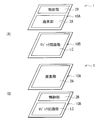
- FIG. 6 is a schematic diagram illustrating a configuration of an imaging apparatus according to first to fourth embodiments of the present disclosure. It is a schematic block diagram of the imaging device shown in FIG. It is a schematic block diagram of the conventional imaging device. It is sectional drawing of the imaging device shown in FIG. 5 is a process diagram illustrating a method for manufacturing a semiconductor device according to a first embodiment of the present disclosure. FIG. It is process drawing following FIG. 5A. It is process drawing following FIG. 5B.
- FIG. 11 is a process diagram illustrating another example of the method for manufacturing the semiconductor device according to the first embodiment of the present disclosure. It is process drawing following FIG. 6A. It is process drawing following FIG. 6B.
- FIG. 6 is a schematic diagram illustrating a configuration of an imaging apparatus according to first to fourth embodiments of the present disclosure. It is a schematic block diagram of the imaging device shown in FIG. It is a schematic block diagram of the conventional imaging device. It is sectional drawing of the imaging device shown in FIG. 5 is a process diagram illustrating a
- FIG. 10 is a process diagram illustrating a method for manufacturing a semiconductor device according to a second embodiment of the present disclosure. It is process drawing following FIG. 7A. It is process drawing following FIG. 7B.
- FIG. 7D is a process diagram following FIG. 7C. It is a flowchart showing a manufacturing method of a semiconductor device concerning a 3rd embodiment of this indication. It is process drawing following FIG. 8A. It is process drawing following FIG. 8B. It is a flowchart showing a manufacturing method of a semiconductor device concerning a 4th embodiment of this indication. It is process drawing following FIG. 9A. It is process drawing following FIG. 9B. It is a functional block diagram of the electronic device (camera) which concerns on an application example.
- FIG. 1 shows the overall configuration of a MOS solid-state imaging device (imaging device 1) to which semiconductor devices according to first to fourth embodiments of the present disclosure to be described later are applied.
- This imaging device 1 is an imaging device suitable for photographing color images (still images or moving images), and includes a pixel region 3 (so-called pixel array) and a peripheral region 4.
- the pixel region 3 includes a plurality of pixels 2 including photoelectric conversion portions arranged in a matrix on a substrate.
- the pixel 2 provided in the pixel region 3 is provided with a photodiode PD serving as a photoelectric conversion unit, a plurality of pixel transistors Tr (MOS transistors), and the like.
- the plurality of pixel transistors Tr are, for example, three types of transistors, that is, a transfer transistor, a reset transistor, and an amplification transistor. In addition to this, a selection transistor is added to form the four types of transistors. Since the equivalent circuit of the unit pixel is the same as usual, detailed description is omitted.
- the pixel 2 can be configured as one unit pixel, but may have a pixel sharing structure. In this pixel sharing structure, a plurality of photodiodes PD share a floating diffusion constituting a transfer transistor and other transistors other than the transfer transistor.
- the peripheral area 4 is provided with a control circuit 5, a vertical drive circuit 6, a column signal processing circuit 7, a horizontal drive circuit 8, an output circuit 9, and the like.
- the control circuit 5 receives data for instructing an input clock, an operation mode, and the like, and outputs data such as internal information of the imaging apparatus 1. Specifically, the control circuit 5 is based on the vertical synchronization signal, the horizontal synchronization signal, and the master clock, and the clock signal or the reference signal for the operations of the vertical drive circuit 6, the column signal processing circuit 7, the horizontal drive circuit 8, and the like. Generate a control signal. The clock signal and control signal are input to the vertical drive circuit 6, the column signal processing circuit 7, the horizontal drive circuit 8, and the like.
- the vertical drive circuit 6 is constituted by a shift register, for example.
- the vertical drive circuit 6 selects a pixel drive wiring, supplies a pulse for driving the pixel to the selected pixel drive wiring, and drives the pixels in units of rows.
- the vertical drive circuit 6 selectively scans each pixel 2 in the pixel region 3 sequentially in the vertical direction in units of rows, and generates it according to the amount of light received by the photodiode PD of each pixel 2 through the vertical signal line 9.
- a pixel signal based on the signal charge is supplied to the column signal processing circuit 7.
- the column signal processing circuit 7 is arranged for each column of the pixels 2 and performs signal processing such as noise removal on the signal output from the pixels 2 for one row for each pixel column. Specifically, the column signal processing circuit 7 performs signal processing such as CDS for removing fixed pattern noise unique to the pixel 2, signal amplification, and AD conversion.
- a horizontal selection switch (not shown) is connected to the horizontal signal line 10 at the output stage of the column signal processing circuit 7.
- the horizontal drive circuit 8 is constituted by a shift register, for example, and sequentially selects each column signal processing circuit 7 by sequentially outputting horizontal scanning pulses, and a pixel signal from each of the column signal processing circuits 7 is applied to the horizontal signal line 10. It is what is output.
- the output circuit 9 performs signal processing on the signals sequentially supplied from the column signal processing circuits 7 through the horizontal signal lines 10 and outputs the signals.
- the output circuit 9 may perform only buffering, or may perform black level adjustment, column variation correction, various digital signal processing, and the like.
- the input / output terminal 12 exchanges signals with the outside.
- FIG. 2A and 2B show a schematic configuration of the imaging apparatus 1 to which the semiconductor device according to the first to fourth embodiments of the present disclosure is applied.
- FIG. 3 shows a conventional MOS type.
- 1 illustrates a schematic configuration of a solid-state imaging device (imaging device 100).
- a pixel sparse part 102A, a control part 102B, and a logic circuit LC for signal processing are formed in a single semiconductor substrate 110.
- the image sensor 110 includes a pixel region 113 and a control circuit 115.
- the pixel unit 2A, the control unit 2B, and the logic circuit unit LC include two substrates (for example, the first semiconductor substrate 10A and the second semiconductor substrate). 10B). Specifically, the pixel portion 2A and the control portion 2B are formed on the first semiconductor substrate 10A, and a logic circuit LC including a signal processing circuit for signal processing is formed on the second semiconductor substrate 10B.
- the semiconductor substrate 10A and the second semiconductor substrate 10B are configured to be electrically connected to each other.
- the combination of the pixel portion 2A, the control portion 2B, and the logic circuit LC that are separately formed on the first semiconductor substrate 10A and the second semiconductor substrate 10B is not particularly limited.
- the pixel unit 2A may be formed on the first semiconductor substrate 10A
- the control unit 2B and the logic circuit LC may be formed on the second semiconductor substrate 10B.
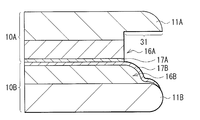
- FIG. 4 shows a part of a cross-sectional configuration of the imaging device 1 based on the configuration of FIG.
- the imaging device 1 is stacked up and down in a state where the first semiconductor substrate 10A on which the pixel unit 2A and the control unit 2B are formed and the second semiconductor substrate 10B on which the logic circuit LC is formed are electrically connected. ing.
- the imaging apparatus 1 has an element formation surface (device layers 16A and 16B) on which the second semiconductor substrate 10B is located and the MOS transistors Tr of the second semiconductor substrate 10B and the first semiconductor substrate 10A are formed. It is what was joined facing and laminated
- the photodiode PD that is a photoelectric conversion unit is disposed on the front surface (the upper surface in the figure, hereinafter referred to as the back surface) side on the first semiconductor substrate 10A side.
- Insulating layers 13A and 13B in which multilayer wiring layers 14A and 14B are formed are formed on the bonding surface between the first semiconductor substrate 10A and the second semiconductor substrate 10B.
- the MOS transistor Tr provided in the pixel portion 2A and the control portion 2B in the pixel region 3 has a gate electrode (both not shown) formed on the pair of source and drain electrodes via a gate insulating film. Have a configuration. Further, on the back surface of the first semiconductor substrate 10A, for example, an antireflection film 18, an insulating film 19 provided with a light shielding film 19A, and a planarizing film 20 are formed. An on-chip lens 22 is provided through a color filter 21 at a position corresponding to the photodiode PD of each pixel 2 on the planarizing film 20.
- the photodiode PD is irradiated with light from the back surface side of the first semiconductor substrate 10A through the on-chip lens, and a signal charge is generated for each pixel 2.
- image data can be obtained by reading image signals from all the pixels 2 as voltage signals corresponding to the signal charges.
- an image sensor that is, a pixel unit 2A and a control unit 2B are formed in an element formation region on the substrate 11A.
- each pixel transistor Tr is formed in the pixel unit 2A.
- the pixel transistor Tr adjacent to the photodiode PD corresponds to a transfer transistor, and its source / drain region (not shown) corresponds to a floating diffusion FD.
- the MOS transistor Tr is formed in the control unit 2B.
- Each MOS transistor Tr is composed of, for example, a pair of n-type source / drain regions and a gate electrode (both not shown) formed via a gate insulating film.
- connection hole 15A is formed, and a connection conductor 15 connected to a predetermined transistor is formed.
- a metal layer made of a plurality of layers, for example, three layers of copper or the like is formed so as to connect the connection conductors 15 to form a wiring layer 14A.
- the first semiconductor substrate 10A having the pixel unit 2A and the control unit 2B is formed.
- a logic circuit LC including a column signal processing circuit 7 for signal processing is formed in the element formation region on the substrate 11B.
- a plurality of MOS transistors Tr constituting the logic circuit LC are formed on the substrate 11B.
- Each MOS transistor Tr is composed of, for example, a pair of n-type source / drain regions and a gate electrode (both not shown) formed via a gate insulating film.
- the insulating layer 13B, the connection hole 15A, the connection conductor 15 and the wiring layer 14B are formed on the substrate 11B by the same method as the first semiconductor substrate 10A.
- the second semiconductor substrate 10B having the logic circuit LC is formed.
- a stress correction film (not shown) may be formed on the wiring layer 14B in order to reduce stress during bonding between a first semiconductor substrate 10A and a second semiconductor substrate 10B described later.
- a P—SiN film plasma nitride film
- a P—SiON film plasma oxynitride film
- first semiconductor substrate 10A and second semiconductor substrate 10B are bonded together so that the wiring layers 14A and 14B face each other.
- an adhesive layer (not shown) is formed on one side of the bonding surface of the first semiconductor substrate 10A or the second semiconductor substrate 10B, and the semiconductor substrates 10A and 10B are formed via the adhesive layer.
- the first semiconductor substrate 10A on which the pixel region 3 is formed is disposed on the upper layer
- the second semiconductor substrate 10B is disposed on the lower layer and bonded together.
- the first semiconductor substrate 10A and the second semiconductor substrate 10B may be bonded using plasma bonding in addition to the bonding via the adhesive layer.
- plasma bonding a plasma SiO 2 film, a SiN film, a SiC film, a SiCN film, or the like is formed on the bonding surface between the first semiconductor substrate 10A and the second semiconductor substrate 10B.
- the first semiconductor substrate 10A and the second semiconductor substrate 10B are joined by annealing.
- the annealing treatment is preferably performed by a low-temperature process of 400 ° C. or lower that does not affect the wiring or the like.
- the back surface side (substrate 11A side) of the first semiconductor substrate 10A is ground and polished to thin the first semiconductor substrate 10A. Specifically, this thinning reduces the thickness of the substrate 11A having a thickness of, for example, about 600 ⁇ m to about 3 to 6 ⁇ m so that the photodiode PD faces.
- the back surface of the first semiconductor substrate 10 ⁇ / b> A becomes the light incident surface of the back-illuminated image sensor 1.
- an insulating film 19 provided with an antireflection film 18, a light shielding film 19A, a planarizing film 20, and the like are formed on the back surface of the first semiconductor substrate 10A. Further, the imaging device 1 is completed by forming the red (R), green (G), and blue (B) color filters 21 and the on-chip lens 22 corresponding to each pixel on the planarizing film 20.
- first to fourth embodiments methods for thinning the first semiconductor substrate 10A will be described as first to fourth embodiments according to a method for manufacturing a semiconductor device of the present disclosure.
- the same components as those of the imaging device 1 described above are denoted by the same reference numerals, and description thereof will be omitted as appropriate.
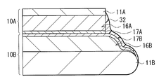
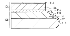
- First Embodiment> 5A to 5C show a method of manufacturing a semiconductor device according to the first embodiment of the present disclosure, in particular, a process of thinning the first semiconductor substrate 10A.
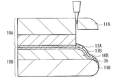
- the end portion of the first semiconductor substrate 10A is removed within a range of, for example, a width of 2 mm and a depth of 100 ⁇ m to form a thin portion 31.
- the first semiconductor substrate 10A and the second semiconductor substrate 10B are bonded together using, for example, the above-described plasma bonding.
- the first semiconductor substrate 10A is ground and the entire surface of the substrate is mechanically thinned, and then, for example, the first semiconductor substrate 10A is subjected to the first using an ion beam method (see Japanese Patent Laid-Open No. 2010-70788).
- a 3 ⁇ m-thick SiN film (protective film 32) is formed on the side surface of the semiconductor substrate 10A and the surface of the second semiconductor substrate 10B.
- the protective film 32 covers the surface of the second semiconductor substrate 10B together with the broken pieces when the broken pieces of the substrate 11A pierce the surface of the second semiconductor substrate 10B during the grinding of the first semiconductor substrate 10A.
- the protective film 32 As a material constituting the protective film 32, it is preferable to use a material having resistance to a chemical solution (for example, an acid-based chemical solution) used in a chemical treatment on the back surface of the first semiconductor substrate 10A to be performed later.
- a chemical solution for example, an acid-based chemical solution
- Specific examples of the material include a plasma SiN film, SiC, and SiCN.
- the surface of the substrate 11A is smoothed and further thinned by chemical treatment.
- the chemical solution soaks into the damaged portion caused by the substrate 11A and is formed at the end of the second semiconductor substrate 10B. Elution of the metal constituting the wiring layer 14B that is present may occur and contamination may occur.
- the protective film 32 is formed on the surface of the second semiconductor substrate 20B after the removal of the end portion (thin portion 31) of the first semiconductor substrate 10A. The damaged part is sealed with a protective film 32. Thereby, metal contamination due to elution of the wiring layer 14B is prevented.
- the protective film 32 is formed after removing the thin portion 31 of the first semiconductor substrate 10A and thinning the entire surface of the substrate 11A.
- the first semiconductor substrate 10A The protective film 32 of the present embodiment may be formed at the end of the second semiconductor substrate 10B before the bonding between the first semiconductor substrate 10B and the second semiconductor substrate 10B.
- the thin portion 31 is formed at the end of the first semiconductor substrate 10A, the substrate 11A is ground, the thin portion, and the thin portion 31 is removed.
- the method for forming the protective film 32 is not particularly limited as long as the protective film 32 can be locally formed at the end of the second semiconductor substrate 10B.
- a chemical vapor deposition method in which local plasma and a deposition gas are blown to the end portion can be given.
- a method of forming a film may be used.
- this method is based on the premise that the end portions of the laminated upper layer substrate and lower layer substrate are bonded to each other, and that the insulating film on the upper layer substrate side remaining at the end portion can be removed with a chemical solution for removing the upper layer substrate. It has become.
- a step is formed at the end when the element is manufactured, and thus the end is usually in an unjoined state.
- the SiN film which is an insulating film formed on each layer of the element, is not removed by the chemical solution, this method has no effect other than simply creating a dust source at the end.
- the protective film 32 is formed at the end of the second semiconductor substrate 10B before the thinning process of the upper first semiconductor substrate 10A by chemical treatment.
- this protective film 32 By forming this protective film 32, the damaged portion of the second semiconductor substrate 10B caused by the direct hit of the fragments of the substrate 11A generated in the mechanical grinding of the first semiconductor substrate 10B is covered, and the second chemical processing is performed next. 2 Etching of the semiconductor substrate 10B is prevented. Therefore, contamination by metal elution and dust generation from the damaged portion of the second semiconductor substrate 10B is prevented.
- the protective film 32 is formed on the end portion of the second semiconductor substrate 10B where there is a possibility that the broken pieces may hit directly. Thereby, the etching of the second semiconductor substrate 10B by the chemical liquid is prevented. Therefore, contamination by metal elution and dust generation from the second semiconductor substrate side can be prevented, and the reliability and manufacturing yield of the semiconductor device can be improved.
- the protective film 32 is formed only on the necessary portion of the second semiconductor substrate 10B, so that the protective film is formed over the entire surface of the second semiconductor substrate 10B.
- warpage of the second semiconductor substrate 10B due to the stress of the protective film is suppressed, and handling becomes easy.
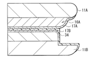
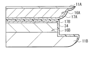
- Second Embodiment> 7A to 7D show a method for manufacturing a semiconductor device according to the second embodiment of the present disclosure, in particular, a step of thinning the first semiconductor substrate.
- the end portion of the second semiconductor substrate 10B before the first semiconductor substrate 10A and the second semiconductor substrate 10B are bonded together, the end portion of the second semiconductor substrate 10B, specifically, the region where the wiring layer 14 is formed is thinned. The point which forms the part 33 and forms the protective film 34 on the whole surface differs from the said embodiment.
- the end portion of the second semiconductor substrate 10B where the wiring layer 14 is formed is thinned by trimming to form a thin portion 33.
- a method other than trimming may be used as a method for forming the thin portion 33.
- a method of applying a polishing process only to a predetermined range (here, an end portion), or an edging method using a dry or wet process may be used.
- a protective film 34 is formed on the entire surface of the second semiconductor substrate 10B, specifically, the side surface exposed by removing the element formation surface and the surface of the thin portion.
- This protective film 34 is made of the same material as that of the protective film 32 formed in the first embodiment, that is, a chemical solution used for thinning the first semiconductor substrate 10A, for example, an acid chemical solution (fluoric nitric acid wet etching solution). For example, a film having a thickness of 10 ⁇ m.
- the protective film 34 As a method for forming the protective film 34, since the upper surface of the second semiconductor substrate 10B after film formation, that is, the element formation surface is a bonding surface, the protective film 34 is uniformly formed so as not to adversely affect the bonding. It is preferable to form a film. Specifically, it is desirable to use an ALD (Atomic Layer Deposition) method with excellent film thickness controllability, but a CVD (Chemical Layer Deposition) method may be used. When using a CVD method or the like, it is desirable to improve the surface flatness by using CMP or the like after film formation.
- ALD Atomic Layer Deposition
- CVD Chemical Layer Deposition
- the protective film 34 it is preferable to smooth and clean the surface of the second semiconductor substrate 10B by a wet process. Specifically, the metal impurities adhering in the case of using machining such as scrubber cleaning or trimming for removing dust on the surface of the second semiconductor substrate 10B are removed. Specifically, it is conceivable to perform a cleaning process using an acid chemical solution (for example, hydrofluoric acid hydrogen peroxide mixed solution (FPM)).
- FPM hydrofluoric acid hydrogen peroxide mixed solution
- the first semiconductor substrate 10A and the second semiconductor substrate 10B are formed.
- the semiconductor substrate 10B is bonded.
- the first semiconductor substrate 10A was thinned.
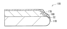
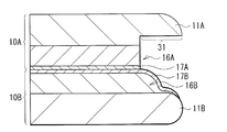
- Third Embodiment> 8A to 8C show a method for manufacturing a semiconductor device according to the third embodiment of the present disclosure, in particular, a step of thinning the first semiconductor substrate 10A.
- the manufacturing method in the present embodiment uses a laser microjet for removing the end portion (thin portion 31) of the first semiconductor substrate 10A.
- the end portion of the first semiconductor substrate 10A is removed within a range of, for example, a width of 2 mm and a depth of 100 ⁇ m to form a thin portion 31.
- the occurrence of damage in the second semiconductor substrate 10B can be suppressed.
- a gap is provided between the first semiconductor substrate 10A and the second semiconductor substrate 10B.
- the laser wavelength penetrates the first semiconductor substrate 10A, and at the same time, a strong spread of the radiant flux occurs, and the strong energy obtained by reflecting the laser cannot be maintained. Thereby, damage to the second semiconductor substrate 10B due to the laser can be suppressed.
- a protective film 35 is formed on the end portion of the second semiconductor substrate 10B.
- This protective film 35 is formed with a thickness of 1 ⁇ m using a material that does not absorb laser light, specifically, SiO 2 , SiN or the like.
- a processing selection ratio is obtained when the thin portion 31 of the first semiconductor substrate 10A is removed by a laser microjet performed in a later step, and the second semiconductor substrate 10B is damaged by the laser light together with the formation of the gap. Is prevented.
- the entire back surface of the first semiconductor substrate 10A is thinned by chemical treatment.
- a method using a laser beam as in the present embodiment is disclosed (see, for example, JP-A-2006-108532). Specifically, the laminated upper layer substrate is irradiated with a laser beam at a predetermined position to remove the end portion of the upper layer substrate, and then the upper layer substrate is ground and thinned. In this method, the edge of the upper layer substrate is removed before the upper layer substrate is ground, so that no knife edge is formed. For this reason, the upper layer substrate can be ground to a predetermined thickness without damaging the surface of the lower layer substrate during grinding.
- the thin portion 31 is formed at the end of the first semiconductor substrate 10A, and the protective film 35 that does not absorb the laser wavelength is provided at the end of the second semiconductor substrate, and then the laser The end portion of the first semiconductor substrate 10A by light was removed.
- the second semiconductor substrate 10B can be processed without being damaged by the laser beam.
- the protective film 35 against the laser beam is formed only on the end portion of the second semiconductor substrate 10B.
- the present invention is not limited to this, and the second semiconductor substrate is bonded before the first semiconductor substrate 10A and the second semiconductor substrate 10B are bonded together. It may be provided on the entire surface of 10B.
- Fourth Embodiment> 9A to 9C show a method for manufacturing a semiconductor device according to the fourth embodiment of the present disclosure, in particular, a step of thinning the first semiconductor substrate 10A.
- the inner region 10a with the end portion remaining on the back surface of the first semiconductor substrate 10A is ground, and after thinning to a predetermined thickness, the end portion is removed.
- the first semiconductor substrate 10A and the second semiconductor substrate 10B are bonded together by using the above-described plasma bonding or the like. Thereafter, as shown in FIG. 9B, the first semiconductor substrate on which the device such as the MOS transistor Tr is formed while leaving the end portion of the first semiconductor substrate 10A causing the damage of the surface of the second semiconductor substrate 10B.
- the inner region 10a of 10A is ground. Subsequently, the inner region 10a is further thinned to a predetermined thickness by wet etching.
- the edge of the first semiconductor substrate 10A is removed by edge trimming.
- the entire surface or the end of the second semiconductor substrate 10B is formed.
- a protective film such as a SiN film may be provided. Thereby, mechanical damage due to debris on the surface of the second semiconductor substrate 10B at the time of removing the end portion of the first semiconductor substrate 10A can be suppressed.
- this method can suppress the knife edge of the upper layer substrate, it cannot avoid the occurrence of damage to the lower layer substrate due to the direct hit of the fragments of the upper layer substrate in the second grinding step. For this reason, contamination due to metal elution or dust generation due to subsequent chemical treatment occurs.
- the inner region where the device is formed is mechanically ground while leaving the end. Subsequently, after the substrate 11A is further thinned to a predetermined thickness by chemical treatment with a chemical solution while leaving the end portion, the end portion of the first semiconductor substrate 10A is removed by edge trimming. By passing through such a process, it becomes possible to prevent the metal elution by chemical
- the imaging device 1 including the semiconductor device formed by using the manufacturing method described in the first to fourth embodiments can be applied to various types of electronic devices having an imaging function, a measurement function, a display function, and the like. is there.
- the imaging apparatus 1 can provide a high-quality color image, it is suitable for a mobile device such as a camera (digital still camera or video camera), a mobile phone having a photographing function, or a PDA (Personal Digital Assistant). is there.
- the present invention can also be applied to a measurement (detection) device for a specific substance.
- FIG. 10 shows a functional block configuration of a camera (camera 200) as an example.
- the camera 200 includes an optical system including a lens group 231 and the like, an imaging device 1, a DSP circuit 232 that is a camera signal processing unit, a frame memory 235, a display device 233, a recording device 236, an operation system 234, a power supply system 237, and the like. Yes.
- the DSP circuit 232, the frame memory 235, the display device 233, the recording device 236, the operation system 234 and the power supply system 237 are configured to be connected to each other via the bus line 38.
- the lens group 231 takes in incident light (image light) from a subject and forms an image on the imaging surface (light receiving surface) of the imaging device 1, and is composed of one or a plurality of lenses.
- the imaging apparatus 1 outputs imaging data D0 based on incident light imaged on the imaging surface by the lens group 231.
- the display device 233 includes, for example, a liquid crystal display device or an organic EL (electroluminescence) display device, and displays a moving image or a still image (color image after image processing by the image processing unit 22) photographed by the imaging device 1. It is.
- the recording device 236 records a moving image or a still image captured by the imaging device 1 on a recording medium such as a video tape or a DVD (Digital Versatile Disk).
- the operation system 234 functions as an external signal input unit in response to an operation by the user, and receives operation commands for various functions of the camera 200 and transmits them to the inside.
- the power supply system 237 includes various power supplies serving as operation power supplies for the DSP circuit 232, the frame memory 235, the display device 233, the recording device 236, and the operation system 234.
- the backside illumination type or the frontside illumination type CMOS is taken as an example of the image sensor.
- the image sensor is not limited to the CMOS, but is a CCD (Charge Coupled Device Image Sensor) or MOS type. It may be an image sensor.
- the present disclosure may be configured as described in the following (1) to (15).
- a method for manufacturing a semiconductor device comprising: a step of forming a protective film; and a step of thinning the first substrate.
- the method for manufacturing a semiconductor device according to (1) Before the step of bonding the first substrate and the second substrate, a step of forming a thin portion at an end portion of the second substrate, and an element of the second substrate exposed by the formation of the thin portion Forming the protective film on the side surface and the surface of the thin portion.
- a method for manufacturing a semiconductor device (11) A step of bonding a first substrate having a first element and a second substrate having a second element with the first element and the second element facing each other, and the end portion of the first substrate A method for manufacturing a semiconductor device, comprising: a step of thinning an inner region excluding a portion; and a step of removing an end portion of the first substrate. (12) The method for manufacturing a semiconductor device according to (11), wherein a protective film is formed on an end portion of the second substrate after bonding the first substrate and the second substrate.
Abstract
Priority Applications (5)
| Application Number | Priority Date | Filing Date | Title |
|---|---|---|---|
| KR1020147018323A KR102079407B1 (ko) | 2012-01-17 | 2013-01-08 | 반도체 장치의 제조 방법 |
| US14/371,550 US9263496B2 (en) | 2012-01-17 | 2013-01-08 | Method of manufacturing an image sensor by joining a pixel circuit substrate and a logic circuit substrate and thereafter thinning the pixel circuit substrate |
| JP2013554264A JP5949784B2 (ja) | 2012-01-17 | 2013-01-08 | 半導体装置の製造方法 |
| CN201380005195.2A CN104040717B (zh) | 2012-01-17 | 2013-01-08 | 半导体装置的制造方法 |
| US14/989,508 US9941326B2 (en) | 2012-01-17 | 2016-01-06 | Method of manufacturing an image sensor by joining a pixel circuit substrate and a logic circuit substrate and thereafter thinning the pixel circuit substrate |
Applications Claiming Priority (6)
| Application Number | Priority Date | Filing Date | Title |
|---|---|---|---|
| JP2012007087 | 2012-01-17 | ||
| JP2012-007087 | 2012-01-17 | ||
| JP2012007088 | 2012-01-17 | ||
| JP2012-007088 | 2012-01-17 | ||
| JP2012007086 | 2012-01-17 | ||
| JP2012-007086 | 2012-01-17 |
Related Child Applications (2)
| Application Number | Title | Priority Date | Filing Date |
|---|---|---|---|
| US14/371,550 A-371-Of-International US9263496B2 (en) | 2012-01-17 | 2013-01-08 | Method of manufacturing an image sensor by joining a pixel circuit substrate and a logic circuit substrate and thereafter thinning the pixel circuit substrate |
| US14/989,508 Continuation US9941326B2 (en) | 2012-01-17 | 2016-01-06 | Method of manufacturing an image sensor by joining a pixel circuit substrate and a logic circuit substrate and thereafter thinning the pixel circuit substrate |
Publications (1)
| Publication Number | Publication Date |
|---|---|
| WO2013108657A1 true WO2013108657A1 (fr) | 2013-07-25 |
Family
ID=48799085
Family Applications (1)
| Application Number | Title | Priority Date | Filing Date |
|---|---|---|---|
| PCT/JP2013/050093 WO2013108657A1 (fr) | 2012-01-17 | 2013-01-08 | Procédé de fabrication pour dispositif à semi-conducteur |
Country Status (5)
| Country | Link |
|---|---|
| US (2) | US9263496B2 (fr) |
| JP (1) | JP5949784B2 (fr) |
| KR (1) | KR102079407B1 (fr) |
| CN (1) | CN104040717B (fr) |
| WO (1) | WO2013108657A1 (fr) |
Cited By (4)
| Publication number | Priority date | Publication date | Assignee | Title |
|---|---|---|---|---|
| WO2015190298A1 (fr) * | 2014-06-11 | 2015-12-17 | ソニー株式会社 | Dispositif à semi-conducteur et son procédé de fabrication |
| JP2016066787A (ja) * | 2014-09-16 | 2016-04-28 | 株式会社東芝 | 電子デバイスの製造方法 |
| JP2021048303A (ja) * | 2019-09-19 | 2021-03-25 | キオクシア株式会社 | 半導体装置 |
| JP2021068744A (ja) * | 2019-10-18 | 2021-04-30 | 株式会社ディスコ | ウェーハの加工方法 |
Families Citing this family (7)
| Publication number | Priority date | Publication date | Assignee | Title |
|---|---|---|---|---|
| KR102524962B1 (ko) * | 2016-11-14 | 2023-04-21 | 삼성전자주식회사 | 기판 구조체 제조 방법 및 이를 이용하여 제조된 기판 구조체 |
| KR20180090494A (ko) * | 2017-02-03 | 2018-08-13 | 삼성전자주식회사 | 기판 구조체 제조 방법 |
| CN108899272A (zh) * | 2018-07-06 | 2018-11-27 | 德淮半导体有限公司 | 用于制造半导体装置的方法 |
| CN109461647A (zh) * | 2018-11-16 | 2019-03-12 | 德淮半导体有限公司 | 半导体装置的制造方法 |
| US10727216B1 (en) | 2019-05-10 | 2020-07-28 | Sandisk Technologies Llc | Method for removing a bulk substrate from a bonded assembly of wafers |
| US20230170353A1 (en) * | 2020-06-18 | 2023-06-01 | Sony Semiconductor Solutions Corporation | Display apparatus, method of manufacturing display apparatus, and electronic apparatus |
| CN111799154A (zh) * | 2020-07-16 | 2020-10-20 | 上海华力微电子有限公司 | 背照式图像传感器的制造方法 |
Citations (4)
| Publication number | Priority date | Publication date | Assignee | Title |
|---|---|---|---|---|
| JP2005285988A (ja) * | 2004-03-29 | 2005-10-13 | Sony Corp | 固体撮像素子とその製造方法、及び半導体集積回路装置とその製造方法 |
| JP2005322745A (ja) * | 2004-05-07 | 2005-11-17 | Sony Corp | 半導体素子、半導体素子の製造方法、固体撮像素子、並びに固体撮像素子の製造方法 |
| JP2007234725A (ja) * | 2006-02-28 | 2007-09-13 | Sony Corp | 固体撮像装置および固体撮像装置の製造方法 |
| JP2012009725A (ja) * | 2010-06-28 | 2012-01-12 | Toshiba Corp | 半導体装置の製造方法、半導体装置およびカメラモジュール |
Family Cites Families (8)
| Publication number | Priority date | Publication date | Assignee | Title |
|---|---|---|---|---|
| JP3849680B2 (ja) * | 2003-10-06 | 2006-11-22 | セイコーエプソン株式会社 | 基板接合体の製造方法、基板接合体、電気光学装置の製造方法、及び電気光学装置 |
| JP4634047B2 (ja) * | 2004-01-23 | 2011-02-16 | パイオニア株式会社 | 集積型半導体発光素子及びその製造方法 |
| JP2009038531A (ja) * | 2007-07-31 | 2009-02-19 | Panasonic Corp | 固体撮像装置及びその駆動方法 |
| JP2010177569A (ja) * | 2009-01-30 | 2010-08-12 | Panasonic Corp | 光学デバイス及びその製造方法 |
| JP5442394B2 (ja) | 2009-10-29 | 2014-03-12 | ソニー株式会社 | 固体撮像装置とその製造方法、及び電子機器 |
| KR101319348B1 (ko) * | 2009-12-21 | 2013-10-16 | 엘지디스플레이 주식회사 | 표시 장치 및 이의 제조 방법 |
| TWI420662B (zh) * | 2009-12-25 | 2013-12-21 | Sony Corp | 半導體元件及其製造方法,及電子裝置 |
| US8502375B2 (en) * | 2010-06-29 | 2013-08-06 | Sandisk Technologies Inc. | Corrugated die edge for stacked die semiconductor package |
-
2013
- 2013-01-08 KR KR1020147018323A patent/KR102079407B1/ko active IP Right Grant
- 2013-01-08 JP JP2013554264A patent/JP5949784B2/ja not_active Expired - Fee Related
- 2013-01-08 WO PCT/JP2013/050093 patent/WO2013108657A1/fr active Application Filing
- 2013-01-08 CN CN201380005195.2A patent/CN104040717B/zh not_active Expired - Fee Related
- 2013-01-08 US US14/371,550 patent/US9263496B2/en not_active Expired - Fee Related
-
2016
- 2016-01-06 US US14/989,508 patent/US9941326B2/en active Active
Patent Citations (4)
| Publication number | Priority date | Publication date | Assignee | Title |
|---|---|---|---|---|
| JP2005285988A (ja) * | 2004-03-29 | 2005-10-13 | Sony Corp | 固体撮像素子とその製造方法、及び半導体集積回路装置とその製造方法 |
| JP2005322745A (ja) * | 2004-05-07 | 2005-11-17 | Sony Corp | 半導体素子、半導体素子の製造方法、固体撮像素子、並びに固体撮像素子の製造方法 |
| JP2007234725A (ja) * | 2006-02-28 | 2007-09-13 | Sony Corp | 固体撮像装置および固体撮像装置の製造方法 |
| JP2012009725A (ja) * | 2010-06-28 | 2012-01-12 | Toshiba Corp | 半導体装置の製造方法、半導体装置およびカメラモジュール |
Cited By (8)
| Publication number | Priority date | Publication date | Assignee | Title |
|---|---|---|---|---|
| WO2015190298A1 (fr) * | 2014-06-11 | 2015-12-17 | ソニー株式会社 | Dispositif à semi-conducteur et son procédé de fabrication |
| CN106463460A (zh) * | 2014-06-11 | 2017-02-22 | 索尼公司 | 半导体装置及其制造方法 |
| US9917091B2 (en) | 2014-06-11 | 2018-03-13 | Sony Corporation | Semiconductor device and method of manufacturing the same |
| JP2016066787A (ja) * | 2014-09-16 | 2016-04-28 | 株式会社東芝 | 電子デバイスの製造方法 |
| JP2021048303A (ja) * | 2019-09-19 | 2021-03-25 | キオクシア株式会社 | 半導体装置 |
| US11621239B2 (en) | 2019-09-19 | 2023-04-04 | Kioxia Corporation | Semiconductor device and method for manufacturing the same |
| JP2021068744A (ja) * | 2019-10-18 | 2021-04-30 | 株式会社ディスコ | ウェーハの加工方法 |
| JP7313775B2 (ja) | 2019-10-18 | 2023-07-25 | 株式会社ディスコ | ウェーハの加工方法 |
Also Published As
| Publication number | Publication date |
|---|---|
| US20160118436A1 (en) | 2016-04-28 |
| US9263496B2 (en) | 2016-02-16 |
| KR102079407B1 (ko) | 2020-02-19 |
| JPWO2013108657A1 (ja) | 2015-12-10 |
| CN104040717B (zh) | 2017-04-05 |
| JP5949784B2 (ja) | 2016-07-13 |
| CN104040717A (zh) | 2014-09-10 |
| US20150004738A1 (en) | 2015-01-01 |
| US9941326B2 (en) | 2018-04-10 |
| KR20140123482A (ko) | 2014-10-22 |
Similar Documents
| Publication | Publication Date | Title |
|---|---|---|
| JP5949784B2 (ja) | 半導体装置の製造方法 | |
| US11637141B2 (en) | Solid-state image pickup apparatus and image pickup system | |
| TWI497696B (zh) | 半導體器件,其製造方法及電子裝置 | |
| TWI442559B (zh) | 固態成像元件及其製造方法,固態成像裝置及成像裝置 | |
| TWI595638B (zh) | 半導體裝置,固態成像裝置及電子設備 | |
| TWI505452B (zh) | 固態成像裝置,固態成像裝置之製造方法,及電子裝備 | |
| KR102133067B1 (ko) | 반도체장치 및 전자기기 | |
| JP6885393B2 (ja) | 固体撮像装置、固体撮像装置の製造方法および電子機器 | |
| TWI443816B (zh) | 固態成像裝置及其製造方法及電子設備 | |
| JP6727948B2 (ja) | 撮像素子、製造方法 | |
| TWI757433B (zh) | 固態影像感測器,製造固態影像感測器之方法,以及電子器件 | |
| JP2012227328A (ja) | 半導体装置、半導体装置の製造方法、固体撮像装置及び電子機器 | |
| JP2007234725A (ja) | 固体撮像装置および固体撮像装置の製造方法 | |
| TW201108405A (en) | Method of manufacturing solid state imaging device, and solid state imaging device | |
| JP2009099875A (ja) | 半導体装置の製造方法 | |
| JP6376245B2 (ja) | 固体撮像装置、および電子機器 | |
| JP2015142067A (ja) | 固体撮像装置およびその製造方法、半導体装置、並びに電子機器 | |
| WO2021090545A1 (fr) | Élément d'imagerie et dispositif d'imagerie | |
| TW202315149A (zh) | 受光元件及電子機器 | |
| JP2005072060A (ja) | 固体撮像素子の製造方法 | |
| JP2009206423A (ja) | 固体撮像素子、固体撮像素子の製造方法および撮像装置 |
Legal Events
| Date | Code | Title | Description |
|---|---|---|---|
| 121 | Ep: the epo has been informed by wipo that ep was designated in this application |
Ref document number: 13738833 Country of ref document: EP Kind code of ref document: A1 |
|
| ENP | Entry into the national phase |
Ref document number: 2013554264 Country of ref document: JP Kind code of ref document: A |
|
| ENP | Entry into the national phase |
Ref document number: 20147018323 Country of ref document: KR Kind code of ref document: A |
|
| WWE | Wipo information: entry into national phase |
Ref document number: 14371550 Country of ref document: US |
|
| NENP | Non-entry into the national phase |
Ref country code: DE |
|
| 122 | Ep: pct application non-entry in european phase |
Ref document number: 13738833 Country of ref document: EP Kind code of ref document: A1 |