US10727216B1 - Method for removing a bulk substrate from a bonded assembly of wafers - Google Patents
Method for removing a bulk substrate from a bonded assembly of wafers Download PDFInfo
- Publication number
- US10727216B1 US10727216B1 US16/409,593 US201916409593A US10727216B1 US 10727216 B1 US10727216 B1 US 10727216B1 US 201916409593 A US201916409593 A US 201916409593A US 10727216 B1 US10727216 B1 US 10727216B1
- Authority
- US
- United States
- Prior art keywords
- wafer
- semiconductor
- substrate
- layer
- semiconductor devices
- Prior art date
- Legal status (The legal status is an assumption and is not a legal conclusion. Google has not performed a legal analysis and makes no representation as to the accuracy of the status listed.)
- Active
Links
- 239000000758 substrate Substances 0.000 title claims abstract description 106
- 238000000034 method Methods 0.000 title claims description 54
- 235000012431 wafers Nutrition 0.000 title description 64
- 239000004065 semiconductor Substances 0.000 claims abstract description 147
- 239000000463 material Substances 0.000 claims abstract description 121
- 239000003989 dielectric material Substances 0.000 claims abstract description 42
- 230000015654 memory Effects 0.000 claims description 47
- 229910052751 metal Inorganic materials 0.000 claims description 28
- 239000002184 metal Substances 0.000 claims description 27
- 230000004888 barrier function Effects 0.000 claims description 22
- VYPSYNLAJGMNEJ-UHFFFAOYSA-N Silicium dioxide Chemical compound O=[Si]=O VYPSYNLAJGMNEJ-UHFFFAOYSA-N 0.000 claims description 19
- 229910052814 silicon oxide Inorganic materials 0.000 claims description 19
- UFHFLCQGNIYNRP-UHFFFAOYSA-N Hydrogen Chemical compound [H][H] UFHFLCQGNIYNRP-UHFFFAOYSA-N 0.000 claims description 7
- 229910052739 hydrogen Inorganic materials 0.000 claims description 7
- 239000001257 hydrogen Substances 0.000 claims description 7
- 230000008021 deposition Effects 0.000 claims description 5
- 230000002093 peripheral effect Effects 0.000 claims description 5
- 230000015572 biosynthetic process Effects 0.000 claims description 3
- 239000000126 substance Substances 0.000 claims description 3
- 229910021419 crystalline silicon Inorganic materials 0.000 claims description 2
- 125000004435 hydrogen atom Chemical group [H]* 0.000 claims description 2
- 230000000737 periodic effect Effects 0.000 claims description 2
- 238000002513 implantation Methods 0.000 claims 1
- 239000002019 doping agent Substances 0.000 description 11
- 239000004020 conductor Substances 0.000 description 6
- NBIIXXVUZAFLBC-UHFFFAOYSA-N Phosphoric acid Chemical compound OP(O)(O)=O NBIIXXVUZAFLBC-UHFFFAOYSA-N 0.000 description 4
- 229910000679 solder Inorganic materials 0.000 description 4
- 229910052581 Si3N4 Inorganic materials 0.000 description 3
- 238000000151 deposition Methods 0.000 description 3
- HQVNEWCFYHHQES-UHFFFAOYSA-N silicon nitride Chemical compound N12[Si]34N5[Si]62N3[Si]51N64 HQVNEWCFYHHQES-UHFFFAOYSA-N 0.000 description 3
- 125000006850 spacer group Chemical group 0.000 description 3
- 229910000147 aluminium phosphate Inorganic materials 0.000 description 2
- 238000003491 array Methods 0.000 description 2
- 239000002178 crystalline material Substances 0.000 description 2
- 238000005137 deposition process Methods 0.000 description 2
- 239000010419 fine particle Substances 0.000 description 2
- 230000006870 function Effects 0.000 description 2
- 239000000203 mixture Substances 0.000 description 2
- 238000012986 modification Methods 0.000 description 2
- 230000004048 modification Effects 0.000 description 2
- 229920002120 photoresistant polymer Polymers 0.000 description 2
- 229910000927 Ge alloy Inorganic materials 0.000 description 1
- 239000005388 borosilicate glass Substances 0.000 description 1
- 238000005229 chemical vapour deposition Methods 0.000 description 1
- 229910052802 copper Inorganic materials 0.000 description 1
- 239000010949 copper Substances 0.000 description 1
- 239000012212 insulator Substances 0.000 description 1
- 238000005259 measurement Methods 0.000 description 1
- 239000007769 metal material Substances 0.000 description 1
- 229910044991 metal oxide Inorganic materials 0.000 description 1
- 150000004706 metal oxides Chemical class 0.000 description 1
- 238000005272 metallurgy Methods 0.000 description 1
- TWNQGVIAIRXVLR-UHFFFAOYSA-N oxo(oxoalumanyloxy)alumane Chemical compound O=[Al]O[Al]=O TWNQGVIAIRXVLR-UHFFFAOYSA-N 0.000 description 1
- 238000004806 packaging method and process Methods 0.000 description 1
- 239000007787 solid Substances 0.000 description 1
- 238000006467 substitution reaction Methods 0.000 description 1
- 230000001052 transient effect Effects 0.000 description 1
- 239000011800 void material Substances 0.000 description 1
Images


Classifications
-
- H—ELECTRICITY
- H01—ELECTRIC ELEMENTS
- H01L—SEMICONDUCTOR DEVICES NOT COVERED BY CLASS H10
- H01L25/00—Assemblies consisting of a plurality of individual semiconductor or other solid state devices ; Multistep manufacturing processes thereof
- H01L25/50—Multistep manufacturing processes of assemblies consisting of devices, each device being of a type provided for in group H01L27/00 or H01L29/00
-
- H—ELECTRICITY
- H01—ELECTRIC ELEMENTS
- H01L—SEMICONDUCTOR DEVICES NOT COVERED BY CLASS H10
- H01L21/00—Processes or apparatus adapted for the manufacture or treatment of semiconductor or solid state devices or of parts thereof
- H01L21/67—Apparatus specially adapted for handling semiconductor or electric solid state devices during manufacture or treatment thereof; Apparatus specially adapted for handling wafers during manufacture or treatment of semiconductor or electric solid state devices or components ; Apparatus not specifically provided for elsewhere
- H01L21/683—Apparatus specially adapted for handling semiconductor or electric solid state devices during manufacture or treatment thereof; Apparatus specially adapted for handling wafers during manufacture or treatment of semiconductor or electric solid state devices or components ; Apparatus not specifically provided for elsewhere for supporting or gripping
- H01L21/6835—Apparatus specially adapted for handling semiconductor or electric solid state devices during manufacture or treatment thereof; Apparatus specially adapted for handling wafers during manufacture or treatment of semiconductor or electric solid state devices or components ; Apparatus not specifically provided for elsewhere for supporting or gripping using temporarily an auxiliary support
-
- H—ELECTRICITY
- H01—ELECTRIC ELEMENTS
- H01L—SEMICONDUCTOR DEVICES NOT COVERED BY CLASS H10
- H01L21/00—Processes or apparatus adapted for the manufacture or treatment of semiconductor or solid state devices or of parts thereof
- H01L21/70—Manufacture or treatment of devices consisting of a plurality of solid state components formed in or on a common substrate or of parts thereof; Manufacture of integrated circuit devices or of parts thereof
- H01L21/77—Manufacture or treatment of devices consisting of a plurality of solid state components or integrated circuits formed in, or on, a common substrate
- H01L21/78—Manufacture or treatment of devices consisting of a plurality of solid state components or integrated circuits formed in, or on, a common substrate with subsequent division of the substrate into plural individual devices
- H01L21/7806—Manufacture or treatment of devices consisting of a plurality of solid state components or integrated circuits formed in, or on, a common substrate with subsequent division of the substrate into plural individual devices involving the separation of the active layers from a substrate
-
- H—ELECTRICITY
- H01—ELECTRIC ELEMENTS
- H01L—SEMICONDUCTOR DEVICES NOT COVERED BY CLASS H10
- H01L21/00—Processes or apparatus adapted for the manufacture or treatment of semiconductor or solid state devices or of parts thereof
- H01L21/70—Manufacture or treatment of devices consisting of a plurality of solid state components formed in or on a common substrate or of parts thereof; Manufacture of integrated circuit devices or of parts thereof
- H01L21/77—Manufacture or treatment of devices consisting of a plurality of solid state components or integrated circuits formed in, or on, a common substrate
- H01L21/78—Manufacture or treatment of devices consisting of a plurality of solid state components or integrated circuits formed in, or on, a common substrate with subsequent division of the substrate into plural individual devices
- H01L21/82—Manufacture or treatment of devices consisting of a plurality of solid state components or integrated circuits formed in, or on, a common substrate with subsequent division of the substrate into plural individual devices to produce devices, e.g. integrated circuits, each consisting of a plurality of components
- H01L21/822—Manufacture or treatment of devices consisting of a plurality of solid state components or integrated circuits formed in, or on, a common substrate with subsequent division of the substrate into plural individual devices to produce devices, e.g. integrated circuits, each consisting of a plurality of components the substrate being a semiconductor, using silicon technology
- H01L21/8221—Three dimensional integrated circuits stacked in different levels
-
- H—ELECTRICITY
- H01—ELECTRIC ELEMENTS
- H01L—SEMICONDUCTOR DEVICES NOT COVERED BY CLASS H10
- H01L24/00—Arrangements for connecting or disconnecting semiconductor or solid-state bodies; Methods or apparatus related thereto
- H01L24/01—Means for bonding being attached to, or being formed on, the surface to be connected, e.g. chip-to-package, die-attach, "first-level" interconnects; Manufacturing methods related thereto
- H01L24/02—Bonding areas ; Manufacturing methods related thereto
- H01L24/07—Structure, shape, material or disposition of the bonding areas after the connecting process
- H01L24/08—Structure, shape, material or disposition of the bonding areas after the connecting process of an individual bonding area
-
- H—ELECTRICITY
- H01—ELECTRIC ELEMENTS
- H01L—SEMICONDUCTOR DEVICES NOT COVERED BY CLASS H10
- H01L24/00—Arrangements for connecting or disconnecting semiconductor or solid-state bodies; Methods or apparatus related thereto
- H01L24/01—Means for bonding being attached to, or being formed on, the surface to be connected, e.g. chip-to-package, die-attach, "first-level" interconnects; Manufacturing methods related thereto
- H01L24/02—Bonding areas ; Manufacturing methods related thereto
- H01L24/07—Structure, shape, material or disposition of the bonding areas after the connecting process
- H01L24/09—Structure, shape, material or disposition of the bonding areas after the connecting process of a plurality of bonding areas
-
- H—ELECTRICITY
- H01—ELECTRIC ELEMENTS
- H01L—SEMICONDUCTOR DEVICES NOT COVERED BY CLASS H10
- H01L24/00—Arrangements for connecting or disconnecting semiconductor or solid-state bodies; Methods or apparatus related thereto
- H01L24/80—Methods for connecting semiconductor or other solid state bodies using means for bonding being attached to, or being formed on, the surface to be connected
-
- H—ELECTRICITY
- H01—ELECTRIC ELEMENTS
- H01L—SEMICONDUCTOR DEVICES NOT COVERED BY CLASS H10
- H01L25/00—Assemblies consisting of a plurality of individual semiconductor or other solid state devices ; Multistep manufacturing processes thereof
- H01L25/03—Assemblies consisting of a plurality of individual semiconductor or other solid state devices ; Multistep manufacturing processes thereof all the devices being of a type provided for in the same subgroup of groups H01L27/00 - H01L33/00, or in a single subclass of H10K, H10N, e.g. assemblies of rectifier diodes
- H01L25/04—Assemblies consisting of a plurality of individual semiconductor or other solid state devices ; Multistep manufacturing processes thereof all the devices being of a type provided for in the same subgroup of groups H01L27/00 - H01L33/00, or in a single subclass of H10K, H10N, e.g. assemblies of rectifier diodes the devices not having separate containers
- H01L25/065—Assemblies consisting of a plurality of individual semiconductor or other solid state devices ; Multistep manufacturing processes thereof all the devices being of a type provided for in the same subgroup of groups H01L27/00 - H01L33/00, or in a single subclass of H10K, H10N, e.g. assemblies of rectifier diodes the devices not having separate containers the devices being of a type provided for in group H01L27/00
- H01L25/0657—Stacked arrangements of devices
-
- H—ELECTRICITY
- H01—ELECTRIC ELEMENTS
- H01L—SEMICONDUCTOR DEVICES NOT COVERED BY CLASS H10
- H01L25/00—Assemblies consisting of a plurality of individual semiconductor or other solid state devices ; Multistep manufacturing processes thereof
- H01L25/18—Assemblies consisting of a plurality of individual semiconductor or other solid state devices ; Multistep manufacturing processes thereof the devices being of types provided for in two or more different subgroups of the same main group of groups H01L27/00 - H01L33/00, or in a single subclass of H10K, H10N
-
- H—ELECTRICITY
- H01—ELECTRIC ELEMENTS
- H01L—SEMICONDUCTOR DEVICES NOT COVERED BY CLASS H10
- H01L27/00—Devices consisting of a plurality of semiconductor or other solid-state components formed in or on a common substrate
- H01L27/02—Devices consisting of a plurality of semiconductor or other solid-state components formed in or on a common substrate including semiconductor components specially adapted for rectifying, oscillating, amplifying or switching and having at least one potential-jump barrier or surface barrier; including integrated passive circuit elements with at least one potential-jump barrier or surface barrier
- H01L27/04—Devices consisting of a plurality of semiconductor or other solid-state components formed in or on a common substrate including semiconductor components specially adapted for rectifying, oscillating, amplifying or switching and having at least one potential-jump barrier or surface barrier; including integrated passive circuit elements with at least one potential-jump barrier or surface barrier the substrate being a semiconductor body
- H01L27/06—Devices consisting of a plurality of semiconductor or other solid-state components formed in or on a common substrate including semiconductor components specially adapted for rectifying, oscillating, amplifying or switching and having at least one potential-jump barrier or surface barrier; including integrated passive circuit elements with at least one potential-jump barrier or surface barrier the substrate being a semiconductor body including a plurality of individual components in a non-repetitive configuration
- H01L27/0688—Integrated circuits having a three-dimensional layout
-
- H—ELECTRICITY
- H10—SEMICONDUCTOR DEVICES; ELECTRIC SOLID-STATE DEVICES NOT OTHERWISE PROVIDED FOR
- H10B—ELECTRONIC MEMORY DEVICES
- H10B43/00—EEPROM devices comprising charge-trapping gate insulators
- H10B43/40—EEPROM devices comprising charge-trapping gate insulators characterised by the peripheral circuit region
-
- H—ELECTRICITY
- H01—ELECTRIC ELEMENTS
- H01L—SEMICONDUCTOR DEVICES NOT COVERED BY CLASS H10
- H01L2221/00—Processes or apparatus adapted for the manufacture or treatment of semiconductor or solid state devices or of parts thereof covered by H01L21/00
- H01L2221/67—Apparatus for handling semiconductor or electric solid state devices during manufacture or treatment thereof; Apparatus for handling wafers during manufacture or treatment of semiconductor or electric solid state devices or components; Apparatus not specifically provided for elsewhere
- H01L2221/683—Apparatus for handling semiconductor or electric solid state devices during manufacture or treatment thereof; Apparatus for handling wafers during manufacture or treatment of semiconductor or electric solid state devices or components; Apparatus not specifically provided for elsewhere for supporting or gripping
- H01L2221/68304—Apparatus for handling semiconductor or electric solid state devices during manufacture or treatment thereof; Apparatus for handling wafers during manufacture or treatment of semiconductor or electric solid state devices or components; Apparatus not specifically provided for elsewhere for supporting or gripping using temporarily an auxiliary support
- H01L2221/68318—Auxiliary support including means facilitating the separation of a device or wafer from the auxiliary support
-
- H—ELECTRICITY
- H01—ELECTRIC ELEMENTS
- H01L—SEMICONDUCTOR DEVICES NOT COVERED BY CLASS H10
- H01L2221/00—Processes or apparatus adapted for the manufacture or treatment of semiconductor or solid state devices or of parts thereof covered by H01L21/00
- H01L2221/67—Apparatus for handling semiconductor or electric solid state devices during manufacture or treatment thereof; Apparatus for handling wafers during manufacture or treatment of semiconductor or electric solid state devices or components; Apparatus not specifically provided for elsewhere
- H01L2221/683—Apparatus for handling semiconductor or electric solid state devices during manufacture or treatment thereof; Apparatus for handling wafers during manufacture or treatment of semiconductor or electric solid state devices or components; Apparatus not specifically provided for elsewhere for supporting or gripping
- H01L2221/68304—Apparatus for handling semiconductor or electric solid state devices during manufacture or treatment thereof; Apparatus for handling wafers during manufacture or treatment of semiconductor or electric solid state devices or components; Apparatus not specifically provided for elsewhere for supporting or gripping using temporarily an auxiliary support
- H01L2221/6835—Apparatus for handling semiconductor or electric solid state devices during manufacture or treatment thereof; Apparatus for handling wafers during manufacture or treatment of semiconductor or electric solid state devices or components; Apparatus not specifically provided for elsewhere for supporting or gripping using temporarily an auxiliary support used as a support during build up manufacturing of active devices
-
- H—ELECTRICITY
- H01—ELECTRIC ELEMENTS
- H01L—SEMICONDUCTOR DEVICES NOT COVERED BY CLASS H10
- H01L2221/00—Processes or apparatus adapted for the manufacture or treatment of semiconductor or solid state devices or of parts thereof covered by H01L21/00
- H01L2221/67—Apparatus for handling semiconductor or electric solid state devices during manufacture or treatment thereof; Apparatus for handling wafers during manufacture or treatment of semiconductor or electric solid state devices or components; Apparatus not specifically provided for elsewhere
- H01L2221/683—Apparatus for handling semiconductor or electric solid state devices during manufacture or treatment thereof; Apparatus for handling wafers during manufacture or treatment of semiconductor or electric solid state devices or components; Apparatus not specifically provided for elsewhere for supporting or gripping
- H01L2221/68304—Apparatus for handling semiconductor or electric solid state devices during manufacture or treatment thereof; Apparatus for handling wafers during manufacture or treatment of semiconductor or electric solid state devices or components; Apparatus not specifically provided for elsewhere for supporting or gripping using temporarily an auxiliary support
- H01L2221/68363—Apparatus for handling semiconductor or electric solid state devices during manufacture or treatment thereof; Apparatus for handling wafers during manufacture or treatment of semiconductor or electric solid state devices or components; Apparatus not specifically provided for elsewhere for supporting or gripping using temporarily an auxiliary support used in a transfer process involving transfer directly from an origin substrate to a target substrate without use of an intermediate handle substrate
-
- H—ELECTRICITY
- H01—ELECTRIC ELEMENTS
- H01L—SEMICONDUCTOR DEVICES NOT COVERED BY CLASS H10
- H01L2221/00—Processes or apparatus adapted for the manufacture or treatment of semiconductor or solid state devices or of parts thereof covered by H01L21/00
- H01L2221/67—Apparatus for handling semiconductor or electric solid state devices during manufacture or treatment thereof; Apparatus for handling wafers during manufacture or treatment of semiconductor or electric solid state devices or components; Apparatus not specifically provided for elsewhere
- H01L2221/683—Apparatus for handling semiconductor or electric solid state devices during manufacture or treatment thereof; Apparatus for handling wafers during manufacture or treatment of semiconductor or electric solid state devices or components; Apparatus not specifically provided for elsewhere for supporting or gripping
- H01L2221/68304—Apparatus for handling semiconductor or electric solid state devices during manufacture or treatment thereof; Apparatus for handling wafers during manufacture or treatment of semiconductor or electric solid state devices or components; Apparatus not specifically provided for elsewhere for supporting or gripping using temporarily an auxiliary support
- H01L2221/68381—Details of chemical or physical process used for separating the auxiliary support from a device or wafer
-
- H—ELECTRICITY
- H01—ELECTRIC ELEMENTS
- H01L—SEMICONDUCTOR DEVICES NOT COVERED BY CLASS H10
- H01L2224/00—Indexing scheme for arrangements for connecting or disconnecting semiconductor or solid-state bodies and methods related thereto as covered by H01L24/00
- H01L2224/01—Means for bonding being attached to, or being formed on, the surface to be connected, e.g. chip-to-package, die-attach, "first-level" interconnects; Manufacturing methods related thereto
- H01L2224/02—Bonding areas; Manufacturing methods related thereto
- H01L2224/04—Structure, shape, material or disposition of the bonding areas prior to the connecting process
- H01L2224/04042—Bonding areas specifically adapted for wire connectors, e.g. wirebond pads
-
- H—ELECTRICITY
- H01—ELECTRIC ELEMENTS
- H01L—SEMICONDUCTOR DEVICES NOT COVERED BY CLASS H10
- H01L2224/00—Indexing scheme for arrangements for connecting or disconnecting semiconductor or solid-state bodies and methods related thereto as covered by H01L24/00
- H01L2224/01—Means for bonding being attached to, or being formed on, the surface to be connected, e.g. chip-to-package, die-attach, "first-level" interconnects; Manufacturing methods related thereto
- H01L2224/02—Bonding areas; Manufacturing methods related thereto
- H01L2224/04—Structure, shape, material or disposition of the bonding areas prior to the connecting process
- H01L2224/05—Structure, shape, material or disposition of the bonding areas prior to the connecting process of an individual bonding area
- H01L2224/0554—External layer
- H01L2224/0556—Disposition
- H01L2224/05568—Disposition the whole external layer protruding from the surface
-
- H—ELECTRICITY
- H01—ELECTRIC ELEMENTS
- H01L—SEMICONDUCTOR DEVICES NOT COVERED BY CLASS H10
- H01L2224/00—Indexing scheme for arrangements for connecting or disconnecting semiconductor or solid-state bodies and methods related thereto as covered by H01L24/00
- H01L2224/01—Means for bonding being attached to, or being formed on, the surface to be connected, e.g. chip-to-package, die-attach, "first-level" interconnects; Manufacturing methods related thereto
- H01L2224/02—Bonding areas; Manufacturing methods related thereto
- H01L2224/07—Structure, shape, material or disposition of the bonding areas after the connecting process
- H01L2224/08—Structure, shape, material or disposition of the bonding areas after the connecting process of an individual bonding area
- H01L2224/081—Disposition
- H01L2224/0812—Disposition the bonding area connecting directly to another bonding area, i.e. connectorless bonding, e.g. bumpless bonding
- H01L2224/08135—Disposition the bonding area connecting directly to another bonding area, i.e. connectorless bonding, e.g. bumpless bonding the bonding area connecting between different semiconductor or solid-state bodies, i.e. chip-to-chip
- H01L2224/08145—Disposition the bonding area connecting directly to another bonding area, i.e. connectorless bonding, e.g. bumpless bonding the bonding area connecting between different semiconductor or solid-state bodies, i.e. chip-to-chip the bodies being stacked
- H01L2224/08147—Disposition the bonding area connecting directly to another bonding area, i.e. connectorless bonding, e.g. bumpless bonding the bonding area connecting between different semiconductor or solid-state bodies, i.e. chip-to-chip the bodies being stacked the bonding area connecting to a bonding area disposed in a recess of the surface of the body
-
- H—ELECTRICITY
- H01—ELECTRIC ELEMENTS
- H01L—SEMICONDUCTOR DEVICES NOT COVERED BY CLASS H10
- H01L2224/00—Indexing scheme for arrangements for connecting or disconnecting semiconductor or solid-state bodies and methods related thereto as covered by H01L24/00
- H01L2224/01—Means for bonding being attached to, or being formed on, the surface to be connected, e.g. chip-to-package, die-attach, "first-level" interconnects; Manufacturing methods related thereto
- H01L2224/02—Bonding areas; Manufacturing methods related thereto
- H01L2224/07—Structure, shape, material or disposition of the bonding areas after the connecting process
- H01L2224/09—Structure, shape, material or disposition of the bonding areas after the connecting process of a plurality of bonding areas
- H01L2224/091—Disposition
- H01L2224/0918—Disposition being disposed on at least two different sides of the body, e.g. dual array
- H01L2224/09181—On opposite sides of the body
-
- H—ELECTRICITY
- H01—ELECTRIC ELEMENTS
- H01L—SEMICONDUCTOR DEVICES NOT COVERED BY CLASS H10
- H01L2224/00—Indexing scheme for arrangements for connecting or disconnecting semiconductor or solid-state bodies and methods related thereto as covered by H01L24/00
- H01L2224/01—Means for bonding being attached to, or being formed on, the surface to be connected, e.g. chip-to-package, die-attach, "first-level" interconnects; Manufacturing methods related thereto
- H01L2224/42—Wire connectors; Manufacturing methods related thereto
- H01L2224/47—Structure, shape, material or disposition of the wire connectors after the connecting process
- H01L2224/48—Structure, shape, material or disposition of the wire connectors after the connecting process of an individual wire connector
- H01L2224/484—Connecting portions
- H01L2224/48475—Connecting portions connected to auxiliary connecting means on the bonding areas, e.g. pre-ball, wedge-on-ball, ball-on-ball
- H01L2224/48476—Connecting portions connected to auxiliary connecting means on the bonding areas, e.g. pre-ball, wedge-on-ball, ball-on-ball between the wire connector and the bonding area
-
- H—ELECTRICITY
- H01—ELECTRIC ELEMENTS
- H01L—SEMICONDUCTOR DEVICES NOT COVERED BY CLASS H10
- H01L2224/00—Indexing scheme for arrangements for connecting or disconnecting semiconductor or solid-state bodies and methods related thereto as covered by H01L24/00
- H01L2224/01—Means for bonding being attached to, or being formed on, the surface to be connected, e.g. chip-to-package, die-attach, "first-level" interconnects; Manufacturing methods related thereto
- H01L2224/42—Wire connectors; Manufacturing methods related thereto
- H01L2224/47—Structure, shape, material or disposition of the wire connectors after the connecting process
- H01L2224/48—Structure, shape, material or disposition of the wire connectors after the connecting process of an individual wire connector
- H01L2224/484—Connecting portions
- H01L2224/48475—Connecting portions connected to auxiliary connecting means on the bonding areas, e.g. pre-ball, wedge-on-ball, ball-on-ball
- H01L2224/48499—Material of the auxiliary connecting means
-
- H—ELECTRICITY
- H01—ELECTRIC ELEMENTS
- H01L—SEMICONDUCTOR DEVICES NOT COVERED BY CLASS H10
- H01L2224/00—Indexing scheme for arrangements for connecting or disconnecting semiconductor or solid-state bodies and methods related thereto as covered by H01L24/00
- H01L2224/73—Means for bonding being of different types provided for in two or more of groups H01L2224/10, H01L2224/18, H01L2224/26, H01L2224/34, H01L2224/42, H01L2224/50, H01L2224/63, H01L2224/71
- H01L2224/732—Location after the connecting process
- H01L2224/73251—Location after the connecting process on different surfaces
-
- H—ELECTRICITY
- H01—ELECTRIC ELEMENTS
- H01L—SEMICONDUCTOR DEVICES NOT COVERED BY CLASS H10
- H01L2224/00—Indexing scheme for arrangements for connecting or disconnecting semiconductor or solid-state bodies and methods related thereto as covered by H01L24/00
- H01L2224/80—Methods for connecting semiconductor or other solid state bodies using means for bonding being attached to, or being formed on, the surface to be connected
- H01L2224/80001—Methods for connecting semiconductor or other solid state bodies using means for bonding being attached to, or being formed on, the surface to be connected by connecting a bonding area directly to another bonding area, i.e. connectorless bonding, e.g. bumpless bonding
- H01L2224/80003—Methods for connecting semiconductor or other solid state bodies using means for bonding being attached to, or being formed on, the surface to be connected by connecting a bonding area directly to another bonding area, i.e. connectorless bonding, e.g. bumpless bonding involving a temporary auxiliary member not forming part of the bonding apparatus
- H01L2224/80006—Methods for connecting semiconductor or other solid state bodies using means for bonding being attached to, or being formed on, the surface to be connected by connecting a bonding area directly to another bonding area, i.e. connectorless bonding, e.g. bumpless bonding involving a temporary auxiliary member not forming part of the bonding apparatus being a temporary or sacrificial substrate
-
- H—ELECTRICITY
- H01—ELECTRIC ELEMENTS
- H01L—SEMICONDUCTOR DEVICES NOT COVERED BY CLASS H10
- H01L2224/00—Indexing scheme for arrangements for connecting or disconnecting semiconductor or solid-state bodies and methods related thereto as covered by H01L24/00
- H01L2224/80—Methods for connecting semiconductor or other solid state bodies using means for bonding being attached to, or being formed on, the surface to be connected
- H01L2224/80001—Methods for connecting semiconductor or other solid state bodies using means for bonding being attached to, or being formed on, the surface to be connected by connecting a bonding area directly to another bonding area, i.e. connectorless bonding, e.g. bumpless bonding
- H01L2224/808—Bonding techniques
- H01L2224/80894—Direct bonding, i.e. joining surfaces by means of intermolecular attracting interactions at their interfaces, e.g. covalent bonds, van der Waals forces
- H01L2224/80895—Direct bonding, i.e. joining surfaces by means of intermolecular attracting interactions at their interfaces, e.g. covalent bonds, van der Waals forces between electrically conductive surfaces, e.g. copper-copper direct bonding, surface activated bonding
-
- H—ELECTRICITY
- H01—ELECTRIC ELEMENTS
- H01L—SEMICONDUCTOR DEVICES NOT COVERED BY CLASS H10
- H01L2224/00—Indexing scheme for arrangements for connecting or disconnecting semiconductor or solid-state bodies and methods related thereto as covered by H01L24/00
- H01L2224/80—Methods for connecting semiconductor or other solid state bodies using means for bonding being attached to, or being formed on, the surface to be connected
- H01L2224/80001—Methods for connecting semiconductor or other solid state bodies using means for bonding being attached to, or being formed on, the surface to be connected by connecting a bonding area directly to another bonding area, i.e. connectorless bonding, e.g. bumpless bonding
- H01L2224/808—Bonding techniques
- H01L2224/80894—Direct bonding, i.e. joining surfaces by means of intermolecular attracting interactions at their interfaces, e.g. covalent bonds, van der Waals forces
- H01L2224/80896—Direct bonding, i.e. joining surfaces by means of intermolecular attracting interactions at their interfaces, e.g. covalent bonds, van der Waals forces between electrically insulating surfaces, e.g. oxide or nitride layers
-
- H—ELECTRICITY
- H01—ELECTRIC ELEMENTS
- H01L—SEMICONDUCTOR DEVICES NOT COVERED BY CLASS H10
- H01L2225/00—Details relating to assemblies covered by the group H01L25/00 but not provided for in its subgroups
- H01L2225/03—All the devices being of a type provided for in the same subgroup of groups H01L27/00 - H01L33/648 and H10K99/00
- H01L2225/04—All the devices being of a type provided for in the same subgroup of groups H01L27/00 - H01L33/648 and H10K99/00 the devices not having separate containers
- H01L2225/065—All the devices being of a type provided for in the same subgroup of groups H01L27/00 - H01L33/648 and H10K99/00 the devices not having separate containers the devices being of a type provided for in group H01L27/00
- H01L2225/06503—Stacked arrangements of devices
- H01L2225/0651—Wire or wire-like electrical connections from device to substrate
-
- H—ELECTRICITY
- H01—ELECTRIC ELEMENTS
- H01L—SEMICONDUCTOR DEVICES NOT COVERED BY CLASS H10
- H01L2225/00—Details relating to assemblies covered by the group H01L25/00 but not provided for in its subgroups
- H01L2225/03—All the devices being of a type provided for in the same subgroup of groups H01L27/00 - H01L33/648 and H10K99/00
- H01L2225/04—All the devices being of a type provided for in the same subgroup of groups H01L27/00 - H01L33/648 and H10K99/00 the devices not having separate containers
- H01L2225/065—All the devices being of a type provided for in the same subgroup of groups H01L27/00 - H01L33/648 and H10K99/00 the devices not having separate containers the devices being of a type provided for in group H01L27/00
- H01L2225/06503—Stacked arrangements of devices
- H01L2225/06513—Bump or bump-like direct electrical connections between devices, e.g. flip-chip connection, solder bumps
-
- H—ELECTRICITY
- H01—ELECTRIC ELEMENTS
- H01L—SEMICONDUCTOR DEVICES NOT COVERED BY CLASS H10
- H01L2225/00—Details relating to assemblies covered by the group H01L25/00 but not provided for in its subgroups
- H01L2225/03—All the devices being of a type provided for in the same subgroup of groups H01L27/00 - H01L33/648 and H10K99/00
- H01L2225/04—All the devices being of a type provided for in the same subgroup of groups H01L27/00 - H01L33/648 and H10K99/00 the devices not having separate containers
- H01L2225/065—All the devices being of a type provided for in the same subgroup of groups H01L27/00 - H01L33/648 and H10K99/00 the devices not having separate containers the devices being of a type provided for in group H01L27/00
- H01L2225/06503—Stacked arrangements of devices
- H01L2225/06524—Electrical connections formed on device or on substrate, e.g. a deposited or grown layer
-
- H—ELECTRICITY
- H01—ELECTRIC ELEMENTS
- H01L—SEMICONDUCTOR DEVICES NOT COVERED BY CLASS H10
- H01L2225/00—Details relating to assemblies covered by the group H01L25/00 but not provided for in its subgroups
- H01L2225/03—All the devices being of a type provided for in the same subgroup of groups H01L27/00 - H01L33/648 and H10K99/00
- H01L2225/04—All the devices being of a type provided for in the same subgroup of groups H01L27/00 - H01L33/648 and H10K99/00 the devices not having separate containers
- H01L2225/065—All the devices being of a type provided for in the same subgroup of groups H01L27/00 - H01L33/648 and H10K99/00 the devices not having separate containers the devices being of a type provided for in group H01L27/00
- H01L2225/06503—Stacked arrangements of devices
- H01L2225/06541—Conductive via connections through the device, e.g. vertical interconnects, through silicon via [TSV]
-
- H—ELECTRICITY
- H01—ELECTRIC ELEMENTS
- H01L—SEMICONDUCTOR DEVICES NOT COVERED BY CLASS H10
- H01L2924/00—Indexing scheme for arrangements or methods for connecting or disconnecting semiconductor or solid-state bodies as covered by H01L24/00
- H01L2924/0001—Technical content checked by a classifier
- H01L2924/00014—Technical content checked by a classifier the subject-matter covered by the group, the symbol of which is combined with the symbol of this group, being disclosed without further technical details
-
- H—ELECTRICITY
- H01—ELECTRIC ELEMENTS
- H01L—SEMICONDUCTOR DEVICES NOT COVERED BY CLASS H10
- H01L2924/00—Indexing scheme for arrangements or methods for connecting or disconnecting semiconductor or solid-state bodies as covered by H01L24/00
- H01L2924/10—Details of semiconductor or other solid state devices to be connected
- H01L2924/11—Device type
- H01L2924/14—Integrated circuits
- H01L2924/143—Digital devices
- H01L2924/1431—Logic devices
-
- H—ELECTRICITY
- H01—ELECTRIC ELEMENTS
- H01L—SEMICONDUCTOR DEVICES NOT COVERED BY CLASS H10
- H01L2924/00—Indexing scheme for arrangements or methods for connecting or disconnecting semiconductor or solid-state bodies as covered by H01L24/00
- H01L2924/10—Details of semiconductor or other solid state devices to be connected
- H01L2924/11—Device type
- H01L2924/14—Integrated circuits
- H01L2924/143—Digital devices
- H01L2924/1434—Memory
- H01L2924/145—Read-only memory [ROM]
- H01L2924/1451—EPROM
- H01L2924/14511—EEPROM
Definitions
- the present disclosure relates generally to the field of semiconductor devices, and in particular, to a method for removing a bulk substrate from a bonded assembly of wafers.
- a three-dimensional memory device including three-dimensional vertical NAND strings having one bit per cell is disclosed in an article by T. Endoh et al., titled “Novel Ultra High Density Memory With A Stacked-Surrounding Gate Transistor (S-SGT) Structured Cell”, IEDM Proc. (2001) 33-36.
- S-SGT Stacked-Surrounding Gate Transistor
- a method of forming a semiconductor structure comprises providing a first wafer including a first substrate, first semiconductor devices overlying the first substrate, and first dielectric material layers and first metal bonding pads overlying the first semiconductor devices, forming a sacrificial material layer over a top surface of a second wafer including a second substrate, forming second semiconductor devices, second dielectric material layers and second metal bonding pads over a top surface of the sacrificial material layer, attaching the second wafer to the first wafer such that the second dielectric material layers face the first dielectric material layers, and the first bonding pads are bonded to the second bonding pads, forming a plurality of voids through the second substrate such that surfaces of the sacrificial material layer are physically exposed underneath the plurality of voids, and removing the sacrificial material layer by providing an etchant that etches a material of the sacrificial material layer through the plurality of voids, wherein the second substrate is detached from
- FIG. 1A is a vertical cross-sectional view of a first die that may be provided in a first wafer according to an embodiment of the present disclosure.
- FIG. 1B is a vertical cross-sectional view of the first wafer that may include a plurality of the first die of FIG. 1A according to an embodiment of the present disclosure.
- FIG. 1C is a top-down view of the first wafer of FIG. 1B .
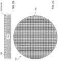
- FIG. 2A is a vertical cross-sectional view of a second die that may be provided in a second wafer according to an embodiment of the present disclosure.
- FIG. 2B is a vertical cross-sectional view of the second wafer that may include a plurality of the second die of FIG. 2A according to an embodiment of the present disclosure.
- FIG. 2C is a top-down view of the second wafer of FIG. 2B .
- FIG. 3 is a perspective view of an exemplary structure including the first wafer and the second wafer prior to bonding the second substrate to the first substrate according to an embodiment of the present disclosure.
- FIG. 4 is a perspective view of an exemplary structure including a bonded assembly of the first wafer and the second wafer after bonding the second substrate to the first substrate according to an embodiment of the present disclosure.
- FIG. 5A is a perspective view of a first configuration of the bonded assembly after forming trenches as voids that extend through a second substrate of the wafer according to a first embodiment of the present disclosure.
- FIG. 5B is a vertical cross-sectional view of the first configuration of the bonded assembly of FIG. 5A .
- FIG. 5C is a top-down view of the first configuration of the bonded assembly of FIGS. 5A and 5B .
- FIG. 6 is a perspective view of the first configuration of the bonded assembly after removing a sacrificial material layer and detaching substrate material strips derived from the second substrate according to the first embodiment of the present disclosure.
- FIG. 7A is a perspective view of a second configuration of the bonded assembly after forming trenches as voids that extend through a second substrate of the wafer according to a second embodiment of the present disclosure.
- FIG. 7B is a vertical cross-sectional view of the second configuration of the bonded assembly of FIG. 7A .
- FIG. 7C is a top-down view of the second configuration of the bonded assembly of FIGS. 7A and 7B .
- FIG. 8 is a perspective view of the second configuration of the bonded assembly after removing a sacrificial material layer and detaching substrate material strips derived from the second substrate according to the second embodiment of the present disclosure.
- FIG. 9 is a vertical cross-sectional view of a bonded die that is present within the bonded assembly provided after the processing steps of FIG. 6 or after the processing steps of FIG. 8 according to an embodiment of the present disclosure.
- FIG. 10 is a vertical cross-sectional view of a bonded die after formation of external bonding pads, solder material portions, and bonding wires according to an embodiment of the present disclosure.
- High performance semiconductor chips may be provided by using a wafer bonding between a first wafer including memory dies and a second wafer including support dies, which are dies including logic devices configured to operate a respective one of the memory dies.
- a bulk substrate of one of the two wafers needs to be removed to provide a thinner layer through which substrate contact via structures are subsequently formed.
- Grinding is typically used to thin the bulk substrate.
- grinding typically involves the removal of a thick layer of a substrate material, which may have a thickness in a range from 500 microns to 1 mm. As such, grinding is time-consuming, costly, and generates fine particles that are difficult to remove and manage.
- a more economical method for removing a bulk substrate from a bonded assembly of two wafers is thus desired.
- the present disclosure is directed to a method for removing a bulk substrate from a bonded assembly of wafers, the various embodiments of which are discussed herein in detail.
- a first element located “on” a second element may be located on the exterior side of a surface of the second element or on the interior side of the second element.
- a first element is located “directly on” a second element if there exist a physical contact between a surface of the first element and a surface of the second element.
- a “prototype” structure or an “in-process” structure refers to a transient structure that is subsequently modified in the shape or composition of at least one component therein.
- a “layer” refers to a material portion including a region having a thickness.
- a layer may extend over the entirety of an underlying or overlying structure, or may have an extent less than the extent of an underlying or overlying structure. Further, a layer may be a region of a homogeneous or inhomogeneous continuous structure that has a thickness less than the thickness of the continuous structure. For example, a layer may be located between any pair of horizontal planes between, or at, a top surface and a bottom surface of the continuous structure. A layer may extend horizontally, vertically, and/or along a tapered surface.
- a substrate may be a layer, may include one or more layers therein, or may have one or more layer thereupon, thereabove, and/or therebelow.
- a first surface and a second surface are “vertically coincident” with each other if the second surface overlies or underlies the first surface and there exists a vertical plane or a substantially vertical plane that includes the first surface and the second surface.
- a substantially vertical plane is a plane that extends straight along a direction that deviates from a vertical direction by an angle less than 5 degrees.
- a vertical plane or a substantially vertical plane is straight along a vertical direction or a substantially vertical direction, and may, or may not, include a curvature along a direction that is perpendicular to the vertical direction or the substantially vertical direction.
- a “memory level” or a “memory array level” refers to the level corresponding to a general region between a first horizontal plane (i.e., a plane parallel to the top surface of the substrate) including topmost surfaces of an array of memory elements and a second horizontal plane including bottommost surfaces of the array of memory elements.
- a “through-stack” element refers to an element that vertically extends through a memory level.
- a “semiconducting material” refers to a material having electrical conductivity in the range from 1.0 ⁇ 10 ⁇ 5 S/m to 1.0 ⁇ 10 5 S/m.
- a “semiconductor material” refers to a material having electrical conductivity in the range from 1.0 ⁇ 10 ⁇ 5 S/m to 1.0 S/m in the absence of electrical dopants therein, and is capable of producing a doped material having electrical conductivity in a range from 1.0 S/m to 1.0 ⁇ 10 5 S/m upon suitable doping with an electrical dopant.
- an “electrical dopant” refers to a p-type dopant that adds a hole to a valence band within a band structure, or an n-type dopant that adds an electron to a conduction band within a band structure.
- a “conductive material” refers to a material having electrical conductivity greater than 1.0 ⁇ 10 5 S/m.
- an “insulator material” or a “dielectric material” refers to a material having electrical conductivity less than 1.0 ⁇ 10 ⁇ 5 S/m.
- a “heavily doped semiconductor material” refers to a semiconductor material that is doped with electrical dopant at a sufficiently high atomic concentration to become a conductive material either as formed as a crystalline material or if converted into a crystalline material through an anneal process (for example, from an initial amorphous state), i.e., to have electrical conductivity greater than 1.0 ⁇ 10 5 S/m.
- a “doped semiconductor material” may be a heavily doped semiconductor material, or may be a semiconductor material that includes electrical dopants (i.e., p-type dopants and/or n-type dopants) at a concentration that provides electrical conductivity in the range from 1.0 ⁇ 10 ⁇ 5 S/m to 1.0 ⁇ 10 5 S/m.
- An “intrinsic semiconductor material” refers to a semiconductor material that is not doped with electrical dopants.
- a semiconductor material may be semiconducting or conductive, and may be an intrinsic semiconductor material or a doped semiconductor material.
- a doped semiconductor material may be semiconducting or conductive depending on the atomic concentration of electrical dopants therein.
- a “metallic material” refers to a conductive material including at least one metallic element therein. All measurements for electrical conductivities are made at the standard condition.
- a monolithic three-dimensional memory array is one in which multiple memory levels are formed above a single substrate, such as a semiconductor wafer, with no intervening substrates.
- the term “monolithic” means that layers of each level of the array are directly deposited on the layers of each underlying level of the array.
- two dimensional arrays may be formed separately and then packaged together to form a non-monolithic memory device.
- non-monolithic stacked memories have been constructed by forming memory levels on separate substrates and vertically stacking the memory levels, as described in U.S. Pat. No.
- the substrates may be thinned or removed from the memory levels before bonding, but as the memory levels are initially formed over separate substrates, such memories are not true monolithic three-dimensional memory arrays.
- the substrate may include integrated circuits fabricated thereon, such as driver circuits for a memory device
- the various three-dimensional memory devices of the present disclosure include a monolithic three-dimensional NAND string memory device, and may be fabricated using the various embodiments described herein.
- the monolithic three-dimensional NAND string is located in a monolithic, three-dimensional array of NAND strings located over the substrate. At least one memory cell in the first device level of the three-dimensional array of NAND strings is located over another memory cell in the second device level of the three-dimensional array of NAND strings.
- a semiconductor package refers to a unit semiconductor device that may be attached to a circuit board through a set of pins or solder balls.
- a semiconductor package may include a semiconductor chip (or a “chip”) or a plurality of semiconductor chips that are bonded throughout, for example, by flip-chip bonding or another chip-to-chip bonding.
- a package or a chip may include a single semiconductor die (or a “die”) or a plurality of semiconductor dies.
- a die is the smallest unit that may independently execute external commands or report status.
- a package or a chip with multiple dies is capable of simultaneously executing as many external commands as the total number of planes therein. Each die includes one or more planes.
- Identical concurrent operations may be executed in each plane within a same die, although there may be some restrictions.
- a die is a memory die, i.e., a die including memory elements
- concurrent read operations, concurrent write operations, or concurrent erase operations may be performed in each plane within a same memory die.
- each plane contains a number of memory blocks (or “blocks”), which are the smallest unit that may be erased by in a single erase operation.
- Each memory block contains a number of pages, which are the smallest units that may be selected for programming.
- a page is also the smallest unit that may be selected to a read operation.
- the first wafer 900 including a two-dimensional array of first semiconductor dies 950 is illustrated.
- the first wafer 900 may be formed by providing a first substrate 908 , and by forming first semiconductor devices 920 , first dielectric material layers 960 , and first metal interconnect structures 980 formed in the first dielectric material layers 960 .
- the first substrate 908 may have a thickness in a range from 300 microns to 2,000 microns, although lesser and greater thicknesses may also be used.
- the first substrate 908 may include a commercially available semiconductor substrate.
- the first substrate 908 may include a first substrate semiconductor layer 909 , which may be the entirety of the first substrate 908 or a top portion of the first substrate 908 .
- the first semiconductor devices 920 may include a three-dimensional array of memory elements such as a three-dimensional NAND memory array.
- the first semiconductor devices 920 may include a peripheral circuitry configured to control operation of a three-dimensional array of memory elements to be provided in another semiconductor die.
- the first semiconductor devices 920 may include a planar insulating spacer 910 located on a top surface of the first substrate semiconductor layer 909 , at least one alternating stack of insulating layers 32 and electrically conductive layers 46 , and memory stack structures 58 vertically extending through the at least one alternating stack ( 32 , 46 ).
- Each memory stack structure 58 may include a memory film, a vertical semiconductor channel contacting the memory film, and a drain region contacting a top end of the vertical semiconductor channel.
- a retro-stepped dielectric material portion 65 may be located over stepped surfaces of the at least one alternating stack ( 32 , 46 ).
- the first dielectric material layers 960 may be formed over the at least one alternating stack ( 32 , 46 ) and the retro-stepped dielectric material portion 65 .
- Various contact via structures ( 86 , 88 ) may be formed to provide electrical contact to various nodes of the first semiconductor devices 920 .
- the various contact via structures ( 86 , 88 ) may include word line contact via structures 86 contacting the electrically conductive layers 46 , which may function as word lines for the three-dimensional array of memory elements located within the memory stack structures 58 .
- the contact via structures ( 86 , 88 ) may include drain contact via structures 88 contacting a respective one of the drain regions.
- the first metal interconnect structures 980 may include bit lines 98 that are connected to a respective subset of the drain contact via structures 88 .
- First metal bonding pads 988 are formed within the first dielectric material layers 960 at a surface portion thereof.
- Each of the first semiconductor dies 950 may comprise a respective subset of the first semiconductor devices 920 .
- Each first semiconductor die 950 may include a set of first metal bonding pads 988 that are physically exposed.
- Each of the first semiconductor dies 950 may include a memory die or a support die that may be bonded to a memory die.
- a second wafer 700 including a two-dimensional array of second semiconductor dies 750 is illustrated.
- the second wafer 700 may be formed by providing a second substrate 708 , and by forming second semiconductor devices 710 , second dielectric material layers 760 , and second metal interconnect structures 780 formed in the second dielectric material layers 760 .
- the second substrate 708 may have a thickness in a range from 300 microns to 2,000 microns, although lesser and greater thicknesses may also be used.
- the second substrate 708 may include a commercially available semiconductor substrate.
- the second substrate 708 may include a second substrate semiconductor layer 709 , which may be the entirety of the second substrate 708 or a top portion of the second substrate 708 .
- a sacrificial material layer 703 may be formed over a top surface of the second substrate 708 .
- the sacrificial material layer 703 may include a material that may be subsequently removed selective to the material of the second substrate semiconductor layer 709 .
- the sacrificial material layer 703 may include silicon nitride, a silico-germanium alloy, or borosilicate glass.
- the sacrificial material layer 703 may have a thickness in a range from 100 nm to 5,000 nm.
- the sacrificial material layer 703 may be deposited by a conformal deposition process or a non-conformal deposition process.
- An etch barrier layer 704 may be optionally formed on a top surface of the sacrificial material layer 703 .
- the etch barrier layer 704 may include a material that is resistant to an etchant to be subsequently used to remove the sacrificial material layer 703 .
- the etch barrier layer 704 may include silicon oxide or a dielectric metal oxide material such as aluminum oxide.
- the thickness of the etch barrier layer 704 may be in a range from 50 nm to 500 nm, although lesser and greater thicknesses may also be used.
- the etch barrier layer 704 may include a silicon oxide layer, which is herein referred to as a first silicon oxide layer.
- a semiconductor material layer 706 may be formed over the sacrificial material layer 703 .
- the semiconductor material layer 706 may be formed directly on a top surface of the etch barrier layer 704 , or may be formed directly on a top surface of the sacrificial material layer 703 in case the etch barrier layer 704 is not used.
- the semiconductor material layer 706 may be formed by providing a single crystalline semiconductor wafer having a second silicon oxide layer on a top portion thereof.
- a hydrogen implanted layer may be formed within the single crystalline semiconductor wafer by implanting hydrogen atoms through the second silicon oxide layer.
- the depth of the hydrogen implanted layer may be in a range from 50 nm to 1,000 nm from the interface between the single crystalline semiconductor wafer and the second silicon oxide layer.
- the second silicon oxide layer may be bonded to the first silicon oxide layer by oxide-to-oxide bonding, which may use a thermal anneal at an elevated temperature that may be in a range from 400 degrees Celsius to 1,000 degrees Celsius.
- the single crystalline semiconductor wafer may include a proximal portion that is more proximal to the bonding interface than the hydrogen implanted layer is to the bonding interface, and a distal portion that is more distal from the bonding interface than the hydrogen implanted layer is from the bonding interface.
- the single crystalline semiconductor wafer may be cleaved at the hydrogen implanted layer during, or after, bonding the proximal portion of the single crystalline semiconductor layer to the first silicon oxide layer though the second silicon oxide layer.
- the distal portion of the single crystalline semiconductor layer is cleaved from the proximal portion of the single crystalline semiconductor layer.
- the proximal portion of the single crystalline semiconductor layer that is attached to the second silicon oxide layer constitutes the semiconductor material layer 706 .
- the semiconductor material layer 706 may include a single crystalline semiconductor material.
- the semiconductor material layer 706 may comprise a polycrystalline semiconductor material layer.
- the semiconductor material layer 706 may be formed by deposition of a polycrystalline semiconductor material on a top surface of the etch barrier layer 704 (or on a top surface of the sacrificial material layer 703 ) or by deposition of an amorphous semiconductor material on the top surface of the etch barrier layer 704 (or on a top surface of the sacrificial material layer 703 ) and a subsequent thermal anneal process that converts the amorphous semiconductor material into a polycrystalline semiconductor material.
- the semiconductor material of the semiconductor material layer 706 may be deposited, for example, by chemical vapor deposition.
- the thickness of the semiconductor material layer 706 may be in a range from 50 nm to 1,000 nm, although lesser and greater thicknesses may also be used.
- Second semiconductor devices 710 and second dielectric material layers 760 may be formed over a top surface of the sacrificial material layer 703 .
- the second semiconductor devices 710 and second dielectric material layers 760 may be formed on a top surface of the semiconductor material layer 706 .
- the second metal interconnect structures 780 may be formed in the second dielectric material layer 760 .
- the second metal interconnect structures 780 may provide electrical interconnection to the various nodes of the second semiconductor devices 710 .
- Second metal bonding pads 788 are formed within the second dielectric material layers 760 at a surface portion thereof.
- a plurality of second semiconductor dies 750 may be formed on the second wafer 700 .
- Each of the second semiconductor dies 750 may comprise a respective subset of the second semiconductor devices 710 .
- Each of the second semiconductor dies 750 may include a memory die or a support die that may be bonded to a memory die.
- Each second semiconductor die 750 may include a set of second metal bonding pads 788 that are physically exposed. The set of second metal bonding pads 788 may have a mirror image pattern of the pattern of a set of first metal bonding pads 988 on each first semiconductor die 950 .
- the first semiconductor devices 920 on the first wafer 900 may comprise a three-dimensional array of memory elements, and the second semiconductor devices 710 on the second wafer 700 may comprise a peripheral circuitry configured to control operation of the three-dimensional array of memory elements.
- the second semiconductor devices 710 of the second wafer 700 may comprise a three-dimensional array of memory elements, and the first semiconductor devices 920 of the first wafer 900 may comprise a peripheral circuitry configured to control operation of the three-dimensional array of memory elements.
- the first wafer 900 and the second wafer 700 may be positioned and orientated such that the physically exposed surface of the first dielectric material layers 960 of the first wafer 900 faces the physically exposed surface of the second dielectric material layers 760 of the second wafer 700 .
- the first wafer 900 and the second wafer 700 may be oriented such that each set of first metal bonding pads 988 on a first semiconductor die 950 faces a respective set of second metal bonding pads 788 on a second semiconductor die 750 .
- each set of first metal bonding pads 988 of the first semiconductor die 950 may be bonded to a respective set of second metal bonding pads 788 of the second semiconductor die 750 by metal-to-metal bonding such as copper-to-copper bonding.
- the second wafer 700 may be attached to the first wafer 900 to form a bonded assembly ( 900 , 700 ) such that the second dielectric material layers 760 face the first dielectric material layers 960 .
- a first configuration of the bonded assembly that may be used to remove the second substrate 708 is illustrated.
- a plurality of voids may be formed through the second substrate 708 such that surfaces of the sacrificial material layer 703 are physically exposed underneath the plurality of voids.
- the maximum lateral distance between each neighboring pair of voids selected from the plurality of voids may be in a range from 1 mm to 25 mm.
- the plurality of voids may be formed as a plurality of trenches 707 having a respective pair of straight edges that laterally extend from one side of a periphery of the second substrate 708 to another side of the periphery of the second substrate 708 .
- Each trench 707 may vertically extend through the entire thickness of the second substrate 708 , and may have a uniform width throughout.
- the straight edges of the plurality of trenches 707 may be substantially vertical and may be parallel to one another.
- the plurality of trenches 707 may be formed by dicing through the second substrate 708 .
- the plurality of trenches 707 may be formed by dicing the second substrate 708 into multiple disjoined substrate material strips 709 ′ using a dicing saw.
- a horizontal surface and a pair of sidewalls of the sacrificial material layer 703 may be physically exposed within each trench 707 .
- the width of each trench 707 may be the same as the width of the blade of the dicing saw, and may be in a range from 50 microns to 2 mm, although lesser and greater widths may also be used.
- the plurality of trenches 707 may be formed by placing the assembly of the first wafer 900 and the second wafer 700 such that the second wafer 700 overlies the first wafer 900 , by covering a top surface of the second wafer 700 with a patterned etch mask layer (such as a lithographically patterned photoresist layer) including line-shaped openings, and by transferring a pattern of the line-shaped openings through the second substrate 708 using an etch process.
- the etch process may use a dry etch process (such as an anisotropic etch process) or a wet etch process.
- a wet etch process using a KOH solution may be used to form the plurality of trenches 707 .
- the plurality of trenches 707 may have tapered sidewalls or contoured sidewalls with a taper angle in a range from 20 degrees to 70 degrees.
- the width of each trench 707 may be in a range from 50 microns to 2 mm, although lesser and greater widths may also be used.
- an isotropic etch process may be performed to apply an isotropic etchant that etches the material of the sacrificial material layer 703 into the plurality of voids through the second substrate 708 , i.e., into the plurality of trenches 707 .
- the isotropic etchant may be provided into the plurality of voids as a wet etch chemical in a wet etch process.
- the isotropic etchant may include hot phosphoric acid.
- the isotropic etchant may etch the material of the sacrificial material layer 703 selective to the material of the etch barrier layer 704 .
- the sacrificial material layer 703 may be removed by the isotropic etch process, and the disjoined substrate material strips 709 ′ derived from the second substrate 708 may be detached from the remaining portions of the bonded assembly including the first wafer 900 , the second semiconductor devices 710 , and the second dielectric material layers 760 upon removal of the sacrificial material layer 703 .
- a second embodiment configuration of the bonded assembly that may be used to remove the second substrate 708 is illustrated.
- a plurality of voids may be formed through the second substrate 708 such that surfaces of the sacrificial material layer 703 may be physically exposed underneath the plurality of voids.
- the maximum lateral distance between each neighboring pair of voids selected from the plurality of voids may be in a range from 1 mm to 25 mm.
- the plurality of voids may be formed as a plurality of pillar-shaped discrete cavities 717 that are laterally spaced apart from one another.
- the plurality of pillar-shaped discrete cavities 717 may be formed as a periodic two-dimensional array of pillar-shaped discrete cavities 717 .
- Each pillar-shaped discrete cavity 717 may vertically extend through the entire thickness of the second substrate 708 .
- the pillar-shaped discrete cavities 717 may have substantially vertical sidewalls.
- the plurality of pillar-shaped discrete cavities 717 may be formed by placing an assembly of the first wafer 900 and the second wafer 700 such that the second wafer 700 overlies the first wafer 900 , by covering a top surface of the second wafer with a patterned etch mask layer (such as a lithographically patterned photoresist layer) including discrete openings, and by transferring a pattern of the discrete openings through the second substrate 708 to form pillar-shaped discrete cavities 717 .
- the etch process may use a dry etch process (such as an anisotropic etch process) or a wet etch process.
- a wet etch process using a KOH solution may be used to form the plurality of trenches 707 .
- the plurality of pillar-shaped discrete cavities 717 may have tapered sidewalls or contoured sidewalls with a taper angle in a range from 20 degrees to 70 degrees.
- the maximum lateral dimension (which may be a diameter) of each trench 707 may be in a range from 50 microns to 2 mm, although lesser and greater widths may also be used.
- an isotropic etch process may be performed to apply an isotropic etchant that etches the material of the sacrificial material layer 703 into the plurality of voids through the second substrate 708 , i.e., into the plurality of pillar-shaped discrete cavities 717 .
- the isotropic etchant may be provided into the plurality of voids as a wet etch chemical in a wet etch process.
- the isotropic etchant may include hot phosphoric acid.
- the isotropic etchant may etch the material of the sacrificial material layer 703 selective to the material of the etch barrier layer 704 .
- the sacrificial material layer 703 may be removed by the isotropic etch process, and a perforated substrate semiconductor layer 709 ′′ derived from the second substrate semiconductor layer 709 may be detached from the remaining portions of the bonded assembly including the first wafer 900 , the second semiconductor devices 710 , and the second dielectric material layers 760 upon removal of the sacrificial material layer 703 .
- the bonded assembly includes a plurality of semiconductor chips including a respective pair of a first semiconductor die 950 and a remaining portion of a second semiconductor die 750 .
- FIG. 9 a semiconductor chip within the bonded assembly of the first wafer 900 and remaining portions of the second wafer 700 is illustrated.
- the structure of FIG. 9 may be derived from the structure of FIG. 6 or from the structure of FIG. 8 .
- a proximal surface of the etch barrier layer 704 that is proximal to the interface between the first dielectric material layers 960 and the second dielectric material layers 760 may contact the semiconductor material layer 706 , and a distal surface of the etch barrier layer 704 may be physically exposed.
- through-substrate via cavities may be formed through the etch barrier layer 704 , the semiconductor material layer 706 , and a subset of layers within the second dielectric material layers 760 to a horizontal surface of a respective one of the second metal interconnect structures 780 .
- a subset of the second metal interconnect structures 780 to which the through-substrate via cavities extend may have pad structures to facilitate formation of conductive via structures thereupon.
- An insulating spacer 711 may be formed at a periphery of each through-substrate via cavity by conformal deposition of a conformal dielectric material layer and by an anisotropic etch process that removes horizontal portions of the conformal dielectric material layer.
- At least one conductive material may be deposited directly on an underlying physically exposed surface of a second metal interconnect structure within each void that is laterally surrounded by an insulating spacer 711 to form a through-substrate via structure 712 .
- An underbump metallurgy (UBM) layer stack may be subsequently deposited over the horizontal portion of the at least one conductive material.
- the UBM layer stack and the at least one conductive material may be patterned over the etch barrier layer 704 to form external bonding pads 716 .
- Solder material portions 718 may be formed on the external bonding pads 716 .
- a bonding wire 719 is attached to each of the solder material portions 718 to electrically connect the external bonding pads 716 to electrical nodes of an external structure such as a packaging substrate or a printed circuit board.
- the various methods of the present disclosure provide easy removal of the second substrate semiconductor layer 709 through use of a plurality of voids ( 707 , 717 ) that extend through the second substrate semiconductor layer 709 .
- a significant portion of the second substrate semiconductor layer 709 may be removed as a solid structure such as the substrate material strips 709 ′ or as the perforated substrate semiconductor layer 709 ′′.
- more than 90%, such as more than 95% and/or more than 98%, of the entire volume of the second substrate semiconductor layer 709 may be removed as the substrate material strips 709 ′ or as the perforated substrate semiconductor layer 709 ′′.
- the methods of the present disclosure do not use grinding, and avoids generation of fine particles from the second substrate semiconductor layer 709 .
- the methods of the present disclosure are environment-friendly as well as being cost-effective compared to prior methods for removing a substrate by grinding.
Abstract
A first wafer including a first substrate, first semiconductor devices overlying the first substrate, and first dielectric material layers overlying the first semiconductor devices is provided. A sacrificial material layer is formed over a top surface of a second wafer including a second substrate. Second semiconductor devices and second dielectric material layers are formed over a top surface of the sacrificial material layer. The second wafer is attached to the first wafer such that the second dielectric material layers face the first dielectric material layers. A plurality of voids is formed through the second substrate. The sacrificial material layer is removed by providing an etchant that etches a material of the sacrificial material layer through the plurality of voids. The substrate is detached from a bonded assembly including the first wafer, the second semiconductor devices, and the second dielectric material layers upon removal of the sacrificial material layer.
Description
The present disclosure relates generally to the field of semiconductor devices, and in particular, to a method for removing a bulk substrate from a bonded assembly of wafers.
A three-dimensional memory device including three-dimensional vertical NAND strings having one bit per cell is disclosed in an article by T. Endoh et al., titled “Novel Ultra High Density Memory With A Stacked-Surrounding Gate Transistor (S-SGT) Structured Cell”, IEDM Proc. (2001) 33-36.
According to an embodiment of the present disclosure, a method of forming a semiconductor structure comprises providing a first wafer including a first substrate, first semiconductor devices overlying the first substrate, and first dielectric material layers and first metal bonding pads overlying the first semiconductor devices, forming a sacrificial material layer over a top surface of a second wafer including a second substrate, forming second semiconductor devices, second dielectric material layers and second metal bonding pads over a top surface of the sacrificial material layer, attaching the second wafer to the first wafer such that the second dielectric material layers face the first dielectric material layers, and the first bonding pads are bonded to the second bonding pads, forming a plurality of voids through the second substrate such that surfaces of the sacrificial material layer are physically exposed underneath the plurality of voids, and removing the sacrificial material layer by providing an etchant that etches a material of the sacrificial material layer through the plurality of voids, wherein the second substrate is detached from a bonded assembly including the first wafer, the second semiconductor devices, the second bonding pads, and the second dielectric material layers upon removal of the sacrificial material layer.
High performance semiconductor chips may be provided by using a wafer bonding between a first wafer including memory dies and a second wafer including support dies, which are dies including logic devices configured to operate a respective one of the memory dies. In such instances where the first wafer is bonded to the second wafer, a bulk substrate of one of the two wafers needs to be removed to provide a thinner layer through which substrate contact via structures are subsequently formed. Grinding is typically used to thin the bulk substrate. However, grinding typically involves the removal of a thick layer of a substrate material, which may have a thickness in a range from 500 microns to 1 mm. As such, grinding is time-consuming, costly, and generates fine particles that are difficult to remove and manage. A more economical method for removing a bulk substrate from a bonded assembly of two wafers is thus desired.
As discussed above, the present disclosure is directed to a method for removing a bulk substrate from a bonded assembly of wafers, the various embodiments of which are discussed herein in detail.
The drawings are not drawn to scale. Multiple instances of an element may be duplicated where a single instance of the element is illustrated, unless absence of duplication of elements is expressly described or clearly indicated otherwise. Ordinals such as “first,” “second,” and “third” are used merely to identify similar elements, and different ordinals may be used across the specification and the claims of the instant disclosure. The same reference numerals refer to the same element or similar element. Unless otherwise indicated, elements having the same reference numerals are presumed to have the same composition and the same function. Unless otherwise indicated, a “contact” between elements refers to a direct contact between elements that provides an edge or a surface shared by the elements. As used herein, a first element located “on” a second element may be located on the exterior side of a surface of the second element or on the interior side of the second element. As used herein, a first element is located “directly on” a second element if there exist a physical contact between a surface of the first element and a surface of the second element. As used herein, a “prototype” structure or an “in-process” structure refers to a transient structure that is subsequently modified in the shape or composition of at least one component therein.
As used herein, a “layer” refers to a material portion including a region having a thickness. A layer may extend over the entirety of an underlying or overlying structure, or may have an extent less than the extent of an underlying or overlying structure. Further, a layer may be a region of a homogeneous or inhomogeneous continuous structure that has a thickness less than the thickness of the continuous structure. For example, a layer may be located between any pair of horizontal planes between, or at, a top surface and a bottom surface of the continuous structure. A layer may extend horizontally, vertically, and/or along a tapered surface. A substrate may be a layer, may include one or more layers therein, or may have one or more layer thereupon, thereabove, and/or therebelow.
As used herein, a first surface and a second surface are “vertically coincident” with each other if the second surface overlies or underlies the first surface and there exists a vertical plane or a substantially vertical plane that includes the first surface and the second surface. A substantially vertical plane is a plane that extends straight along a direction that deviates from a vertical direction by an angle less than 5 degrees. A vertical plane or a substantially vertical plane is straight along a vertical direction or a substantially vertical direction, and may, or may not, include a curvature along a direction that is perpendicular to the vertical direction or the substantially vertical direction.
As used herein, a “memory level” or a “memory array level” refers to the level corresponding to a general region between a first horizontal plane (i.e., a plane parallel to the top surface of the substrate) including topmost surfaces of an array of memory elements and a second horizontal plane including bottommost surfaces of the array of memory elements. As used herein, a “through-stack” element refers to an element that vertically extends through a memory level.
As used herein, a “semiconducting material” refers to a material having electrical conductivity in the range from 1.0×10⁻⁵ S/m to 1.0×10⁵ S/m. As used herein, a “semiconductor material” refers to a material having electrical conductivity in the range from 1.0×10⁻⁵ S/m to 1.0 S/m in the absence of electrical dopants therein, and is capable of producing a doped material having electrical conductivity in a range from 1.0 S/m to 1.0×10⁵ S/m upon suitable doping with an electrical dopant. As used herein, an “electrical dopant” refers to a p-type dopant that adds a hole to a valence band within a band structure, or an n-type dopant that adds an electron to a conduction band within a band structure. As used herein, a “conductive material” refers to a material having electrical conductivity greater than 1.0×10⁵ S/m. As used herein, an “insulator material” or a “dielectric material” refers to a material having electrical conductivity less than 1.0×10⁻⁵ S/m. As used herein, a “heavily doped semiconductor material” refers to a semiconductor material that is doped with electrical dopant at a sufficiently high atomic concentration to become a conductive material either as formed as a crystalline material or if converted into a crystalline material through an anneal process (for example, from an initial amorphous state), i.e., to have electrical conductivity greater than 1.0×10⁵ S/m. A “doped semiconductor material” may be a heavily doped semiconductor material, or may be a semiconductor material that includes electrical dopants (i.e., p-type dopants and/or n-type dopants) at a concentration that provides electrical conductivity in the range from 1.0×10⁻⁵ S/m to 1.0×10⁵ S/m. An “intrinsic semiconductor material” refers to a semiconductor material that is not doped with electrical dopants. Thus, a semiconductor material may be semiconducting or conductive, and may be an intrinsic semiconductor material or a doped semiconductor material. A doped semiconductor material may be semiconducting or conductive depending on the atomic concentration of electrical dopants therein. As used herein, a “metallic material” refers to a conductive material including at least one metallic element therein. All measurements for electrical conductivities are made at the standard condition.
A monolithic three-dimensional memory array is one in which multiple memory levels are formed above a single substrate, such as a semiconductor wafer, with no intervening substrates. The term “monolithic” means that layers of each level of the array are directly deposited on the layers of each underlying level of the array. In contrast, two dimensional arrays may be formed separately and then packaged together to form a non-monolithic memory device. For example, non-monolithic stacked memories have been constructed by forming memory levels on separate substrates and vertically stacking the memory levels, as described in U.S. Pat. No. 5,915,167 titled “Three-dimensional Structure Memory.” The substrates may be thinned or removed from the memory levels before bonding, but as the memory levels are initially formed over separate substrates, such memories are not true monolithic three-dimensional memory arrays. The substrate may include integrated circuits fabricated thereon, such as driver circuits for a memory device
The various three-dimensional memory devices of the present disclosure include a monolithic three-dimensional NAND string memory device, and may be fabricated using the various embodiments described herein. The monolithic three-dimensional NAND string is located in a monolithic, three-dimensional array of NAND strings located over the substrate. At least one memory cell in the first device level of the three-dimensional array of NAND strings is located over another memory cell in the second device level of the three-dimensional array of NAND strings.
Generally, a semiconductor package (or a “package”) refers to a unit semiconductor device that may be attached to a circuit board through a set of pins or solder balls. A semiconductor package may include a semiconductor chip (or a “chip”) or a plurality of semiconductor chips that are bonded throughout, for example, by flip-chip bonding or another chip-to-chip bonding. A package or a chip may include a single semiconductor die (or a “die”) or a plurality of semiconductor dies. A die is the smallest unit that may independently execute external commands or report status. Typically, a package or a chip with multiple dies is capable of simultaneously executing as many external commands as the total number of planes therein. Each die includes one or more planes. Identical concurrent operations may be executed in each plane within a same die, although there may be some restrictions. In case a die is a memory die, i.e., a die including memory elements, concurrent read operations, concurrent write operations, or concurrent erase operations may be performed in each plane within a same memory die. In a memory die, each plane contains a number of memory blocks (or “blocks”), which are the smallest unit that may be erased by in a single erase operation. Each memory block contains a number of pages, which are the smallest units that may be selected for programming. A page is also the smallest unit that may be selected to a read operation.
Referring to FIGS. 1A-1C , a first wafer 900 including a two-dimensional array of first semiconductor dies 950 is illustrated. The first wafer 900 may be formed by providing a first substrate 908, and by forming first semiconductor devices 920, first dielectric material layers 960, and first metal interconnect structures 980 formed in the first dielectric material layers 960. The first substrate 908 may have a thickness in a range from 300 microns to 2,000 microns, although lesser and greater thicknesses may also be used. In one embodiment, the first substrate 908 may include a commercially available semiconductor substrate.
The first substrate 908 may include a first substrate semiconductor layer 909, which may be the entirety of the first substrate 908 or a top portion of the first substrate 908. In one embodiment, the first semiconductor devices 920 may include a three-dimensional array of memory elements such as a three-dimensional NAND memory array. Alternatively, the first semiconductor devices 920 may include a peripheral circuitry configured to control operation of a three-dimensional array of memory elements to be provided in another semiconductor die.
In an illustrative example, the first semiconductor devices 920 may include a planar insulating spacer 910 located on a top surface of the first substrate semiconductor layer 909, at least one alternating stack of insulating layers 32 and electrically conductive layers 46, and memory stack structures 58 vertically extending through the at least one alternating stack (32, 46). Each memory stack structure 58 may include a memory film, a vertical semiconductor channel contacting the memory film, and a drain region contacting a top end of the vertical semiconductor channel. A retro-stepped dielectric material portion 65 may be located over stepped surfaces of the at least one alternating stack (32, 46). The first dielectric material layers 960 may be formed over the at least one alternating stack (32, 46) and the retro-stepped dielectric material portion 65. Various contact via structures (86, 88) may be formed to provide electrical contact to various nodes of the first semiconductor devices 920. For example, the various contact via structures (86, 88) may include word line contact via structures 86 contacting the electrically conductive layers 46, which may function as word lines for the three-dimensional array of memory elements located within the memory stack structures 58. The contact via structures (86, 88) may include drain contact via structures 88 contacting a respective one of the drain regions. The first metal interconnect structures 980 may include bit lines 98 that are connected to a respective subset of the drain contact via structures 88. First metal bonding pads 988 are formed within the first dielectric material layers 960 at a surface portion thereof. Each of the first semiconductor dies 950 may comprise a respective subset of the first semiconductor devices 920. Each first semiconductor die 950 may include a set of first metal bonding pads 988 that are physically exposed. Each of the first semiconductor dies 950 may include a memory die or a support die that may be bonded to a memory die.
Referring to FIGS. 2A-2C , a second wafer 700 including a two-dimensional array of second semiconductor dies 750 is illustrated. The second wafer 700 may be formed by providing a second substrate 708, and by forming second semiconductor devices 710, second dielectric material layers 760, and second metal interconnect structures 780 formed in the second dielectric material layers 760. The second substrate 708 may have a thickness in a range from 300 microns to 2,000 microns, although lesser and greater thicknesses may also be used. In one embodiment, the second substrate 708 may include a commercially available semiconductor substrate. The second substrate 708 may include a second substrate semiconductor layer 709, which may be the entirety of the second substrate 708 or a top portion of the second substrate 708.
A sacrificial material layer 703 may be formed over a top surface of the second substrate 708. The sacrificial material layer 703 may include a material that may be subsequently removed selective to the material of the second substrate semiconductor layer 709. For example, if the second substrate semiconductor layer 709 includes single crystalline silicon, the sacrificial material layer 703 may include silicon nitride, a silico-germanium alloy, or borosilicate glass. The sacrificial material layer 703 may have a thickness in a range from 100 nm to 5,000 nm. The sacrificial material layer 703 may be deposited by a conformal deposition process or a non-conformal deposition process.
An etch barrier layer 704 may be optionally formed on a top surface of the sacrificial material layer 703. The etch barrier layer 704 may include a material that is resistant to an etchant to be subsequently used to remove the sacrificial material layer 703. For example, the etch barrier layer 704 may include silicon oxide or a dielectric metal oxide material such as aluminum oxide. The thickness of the etch barrier layer 704 may be in a range from 50 nm to 500 nm, although lesser and greater thicknesses may also be used. In one embodiment, the etch barrier layer 704 may include a silicon oxide layer, which is herein referred to as a first silicon oxide layer.
A semiconductor material layer 706 may be formed over the sacrificial material layer 703. The semiconductor material layer 706 may be formed directly on a top surface of the etch barrier layer 704, or may be formed directly on a top surface of the sacrificial material layer 703 in case the etch barrier layer 704 is not used.
In one embodiment, the semiconductor material layer 706 may be formed by providing a single crystalline semiconductor wafer having a second silicon oxide layer on a top portion thereof. A hydrogen implanted layer may be formed within the single crystalline semiconductor wafer by implanting hydrogen atoms through the second silicon oxide layer. The depth of the hydrogen implanted layer may be in a range from 50 nm to 1,000 nm from the interface between the single crystalline semiconductor wafer and the second silicon oxide layer. The second silicon oxide layer may be bonded to the first silicon oxide layer by oxide-to-oxide bonding, which may use a thermal anneal at an elevated temperature that may be in a range from 400 degrees Celsius to 1,000 degrees Celsius. The single crystalline semiconductor wafer may include a proximal portion that is more proximal to the bonding interface than the hydrogen implanted layer is to the bonding interface, and a distal portion that is more distal from the bonding interface than the hydrogen implanted layer is from the bonding interface. The single crystalline semiconductor wafer may be cleaved at the hydrogen implanted layer during, or after, bonding the proximal portion of the single crystalline semiconductor layer to the first silicon oxide layer though the second silicon oxide layer. The distal portion of the single crystalline semiconductor layer is cleaved from the proximal portion of the single crystalline semiconductor layer. The proximal portion of the single crystalline semiconductor layer that is attached to the second silicon oxide layer constitutes the semiconductor material layer 706. In this case, the semiconductor material layer 706 may include a single crystalline semiconductor material.
In another embodiment, the semiconductor material layer 706 may comprise a polycrystalline semiconductor material layer. In this case, the semiconductor material layer 706 may be formed by deposition of a polycrystalline semiconductor material on a top surface of the etch barrier layer 704 (or on a top surface of the sacrificial material layer 703) or by deposition of an amorphous semiconductor material on the top surface of the etch barrier layer 704 (or on a top surface of the sacrificial material layer 703) and a subsequent thermal anneal process that converts the amorphous semiconductor material into a polycrystalline semiconductor material. The semiconductor material of the semiconductor material layer 706 may be deposited, for example, by chemical vapor deposition. The thickness of the semiconductor material layer 706 may be in a range from 50 nm to 1,000 nm, although lesser and greater thicknesses may also be used.
A plurality of second semiconductor dies 750 may be formed on the second wafer 700. Each of the second semiconductor dies 750 may comprise a respective subset of the second semiconductor devices 710. Each of the second semiconductor dies 750 may include a memory die or a support die that may be bonded to a memory die. Each second semiconductor die 750 may include a set of second metal bonding pads 788 that are physically exposed. The set of second metal bonding pads 788 may have a mirror image pattern of the pattern of a set of first metal bonding pads 988 on each first semiconductor die 950.
In one embodiment, the first semiconductor devices 920 on the first wafer 900 may comprise a three-dimensional array of memory elements, and the second semiconductor devices 710 on the second wafer 700 may comprise a peripheral circuitry configured to control operation of the three-dimensional array of memory elements. In another embodiment, the second semiconductor devices 710 of the second wafer 700 may comprise a three-dimensional array of memory elements, and the first semiconductor devices 920 of the first wafer 900 may comprise a peripheral circuitry configured to control operation of the three-dimensional array of memory elements.
Referring to FIG. 3 , the first wafer 900 and the second wafer 700 may be positioned and orientated such that the physically exposed surface of the first dielectric material layers 960 of the first wafer 900 faces the physically exposed surface of the second dielectric material layers 760 of the second wafer 700. The first wafer 900 and the second wafer 700 may be oriented such that each set of first metal bonding pads 988 on a first semiconductor die 950 faces a respective set of second metal bonding pads 788 on a second semiconductor die 750.
Referring to FIG. 4 , each set of first metal bonding pads 988 of the first semiconductor die 950 may be bonded to a respective set of second metal bonding pads 788 of the second semiconductor die 750 by metal-to-metal bonding such as copper-to-copper bonding. The second wafer 700 may be attached to the first wafer 900 to form a bonded assembly (900, 700) such that the second dielectric material layers 760 face the first dielectric material layers 960.
Referring to FIGS. 5A-5C , a first configuration of the bonded assembly that may be used to remove the second substrate 708 is illustrated. A plurality of voids may be formed through the second substrate 708 such that surfaces of the sacrificial material layer 703 are physically exposed underneath the plurality of voids. In one embodiment, the maximum lateral distance between each neighboring pair of voids selected from the plurality of voids may be in a range from 1 mm to 25 mm.
In one embodiment, the plurality of voids may be formed as a plurality of trenches 707 having a respective pair of straight edges that laterally extend from one side of a periphery of the second substrate 708 to another side of the periphery of the second substrate 708. Each trench 707 may vertically extend through the entire thickness of the second substrate 708, and may have a uniform width throughout. In one embodiment, the straight edges of the plurality of trenches 707 may be substantially vertical and may be parallel to one another.
In one embodiment, the plurality of trenches 707 may be formed by dicing through the second substrate 708. In this case, the plurality of trenches 707 may be formed by dicing the second substrate 708 into multiple disjoined substrate material strips 709′ using a dicing saw. A horizontal surface and a pair of sidewalls of the sacrificial material layer 703 may be physically exposed within each trench 707. The width of each trench 707 may be the same as the width of the blade of the dicing saw, and may be in a range from 50 microns to 2 mm, although lesser and greater widths may also be used.
In another embodiment, the plurality of trenches 707 may be formed by placing the assembly of the first wafer 900 and the second wafer 700 such that the second wafer 700 overlies the first wafer 900, by covering a top surface of the second wafer 700 with a patterned etch mask layer (such as a lithographically patterned photoresist layer) including line-shaped openings, and by transferring a pattern of the line-shaped openings through the second substrate 708 using an etch process. The etch process may use a dry etch process (such as an anisotropic etch process) or a wet etch process. For example, a wet etch process using a KOH solution may be used to form the plurality of trenches 707. In this case, the plurality of trenches 707 may have tapered sidewalls or contoured sidewalls with a taper angle in a range from 20 degrees to 70 degrees. The width of each trench 707 may be in a range from 50 microns to 2 mm, although lesser and greater widths may also be used.
Referring to FIG. 6 , an isotropic etch process may be performed to apply an isotropic etchant that etches the material of the sacrificial material layer 703 into the plurality of voids through the second substrate 708, i.e., into the plurality of trenches 707. In one embodiment, the isotropic etchant may be provided into the plurality of voids as a wet etch chemical in a wet etch process. For example, if the sacrificial material layer 703 includes silicon nitride, the isotropic etchant may include hot phosphoric acid. The isotropic etchant may etch the material of the sacrificial material layer 703 selective to the material of the etch barrier layer 704. The sacrificial material layer 703 may be removed by the isotropic etch process, and the disjoined substrate material strips 709′ derived from the second substrate 708 may be detached from the remaining portions of the bonded assembly including the first wafer 900, the second semiconductor devices 710, and the second dielectric material layers 760 upon removal of the sacrificial material layer 703.
Referring to FIGS. 7A-7C , a second embodiment configuration of the bonded assembly that may be used to remove the second substrate 708 is illustrated. A plurality of voids may be formed through the second substrate 708 such that surfaces of the sacrificial material layer 703 may be physically exposed underneath the plurality of voids. In one embodiment, the maximum lateral distance between each neighboring pair of voids selected from the plurality of voids may be in a range from 1 mm to 25 mm.
In such an embodiment, the plurality of voids may be formed as a plurality of pillar-shaped discrete cavities 717 that are laterally spaced apart from one another. In one embodiment, the plurality of pillar-shaped discrete cavities 717 may be formed as a periodic two-dimensional array of pillar-shaped discrete cavities 717. Each pillar-shaped discrete cavity 717 may vertically extend through the entire thickness of the second substrate 708. In one embodiment, the pillar-shaped discrete cavities 717 may have substantially vertical sidewalls.
In an embodiment, the plurality of pillar-shaped discrete cavities 717 may be formed by placing an assembly of the first wafer 900 and the second wafer 700 such that the second wafer 700 overlies the first wafer 900, by covering a top surface of the second wafer with a patterned etch mask layer (such as a lithographically patterned photoresist layer) including discrete openings, and by transferring a pattern of the discrete openings through the second substrate 708 to form pillar-shaped discrete cavities 717. The etch process may use a dry etch process (such as an anisotropic etch process) or a wet etch process. For example, a wet etch process using a KOH solution may be used to form the plurality of trenches 707. In this case, the plurality of pillar-shaped discrete cavities 717 may have tapered sidewalls or contoured sidewalls with a taper angle in a range from 20 degrees to 70 degrees. The maximum lateral dimension (which may be a diameter) of each trench 707 may be in a range from 50 microns to 2 mm, although lesser and greater widths may also be used.
Referring to FIG. 8 , an isotropic etch process may be performed to apply an isotropic etchant that etches the material of the sacrificial material layer 703 into the plurality of voids through the second substrate 708, i.e., into the plurality of pillar-shaped discrete cavities 717. In one embodiment, the isotropic etchant may be provided into the plurality of voids as a wet etch chemical in a wet etch process. For example, if the sacrificial material layer 703 includes silicon nitride, the isotropic etchant may include hot phosphoric acid. The isotropic etchant may etch the material of the sacrificial material layer 703 selective to the material of the etch barrier layer 704. The sacrificial material layer 703 may be removed by the isotropic etch process, and a perforated substrate semiconductor layer 709″ derived from the second substrate semiconductor layer 709 may be detached from the remaining portions of the bonded assembly including the first wafer 900, the second semiconductor devices 710, and the second dielectric material layers 760 upon removal of the sacrificial material layer 703.
The bonded assembly includes a plurality of semiconductor chips including a respective pair of a first semiconductor die 950 and a remaining portion of a second semiconductor die 750.
Referring to FIG. 9 , a semiconductor chip within the bonded assembly of the first wafer 900 and remaining portions of the second wafer 700 is illustrated. The structure of FIG. 9 may be derived from the structure of FIG. 6 or from the structure of FIG. 8 . A proximal surface of the etch barrier layer 704 that is proximal to the interface between the first dielectric material layers 960 and the second dielectric material layers 760 may contact the semiconductor material layer 706, and a distal surface of the etch barrier layer 704 may be physically exposed.
Referring to FIG. 10 , through-substrate via cavities may be formed through the etch barrier layer 704, the semiconductor material layer 706, and a subset of layers within the second dielectric material layers 760 to a horizontal surface of a respective one of the second metal interconnect structures 780. In one embodiment, a subset of the second metal interconnect structures 780 to which the through-substrate via cavities extend may have pad structures to facilitate formation of conductive via structures thereupon. An insulating spacer 711 may be formed at a periphery of each through-substrate via cavity by conformal deposition of a conformal dielectric material layer and by an anisotropic etch process that removes horizontal portions of the conformal dielectric material layer. At least one conductive material may be deposited directly on an underlying physically exposed surface of a second metal interconnect structure within each void that is laterally surrounded by an insulating spacer 711 to form a through-substrate via structure 712.
An underbump metallurgy (UBM) layer stack may be subsequently deposited over the horizontal portion of the at least one conductive material. The UBM layer stack and the at least one conductive material may be patterned over the etch barrier layer 704 to form external bonding pads 716. Solder material portions 718 may be formed on the external bonding pads 716. A bonding wire 719 is attached to each of the solder material portions 718 to electrically connect the external bonding pads 716 to electrical nodes of an external structure such as a packaging substrate or a printed circuit board.
The various methods of the present disclosure provide easy removal of the second substrate semiconductor layer 709 through use of a plurality of voids (707, 717) that extend through the second substrate semiconductor layer 709. A significant portion of the second substrate semiconductor layer 709 may be removed as a solid structure such as the substrate material strips 709′ or as the perforated substrate semiconductor layer 709″. In one embodiment, more than 90%, such as more than 95% and/or more than 98%, of the entire volume of the second substrate semiconductor layer 709 may be removed as the substrate material strips 709′ or as the perforated substrate semiconductor layer 709″. Thus, the amount of material of the second substrate semiconductor layer 709 that is removed by an etch process may be minimized. Further, the methods of the present disclosure do not use grinding, and avoids generation of fine particles from the second substrate semiconductor layer 709. Thus, the methods of the present disclosure are environment-friendly as well as being cost-effective compared to prior methods for removing a substrate by grinding.
Although the foregoing refers to particular embodiments, it will be understood that the disclosure is not so limited. It will occur to those of ordinary skill in the art that various modifications may be made to the disclosed embodiments and that such modifications are intended to be within the scope of the disclosure. Compatibility is presumed among all embodiments that are not alternatives of one another. The word “comprise” or “include” contemplates all embodiments in which the word “consist essentially of” or the word “consists of” replaces the word “comprise” or “include,” unless explicitly stated otherwise. Where an embodiment using a particular structure and/or configuration is illustrated in the present disclosure, it is understood that the present disclosure may be practiced with any other compatible structures and/or configurations that are functionally equivalent provided that such substitutions are not explicitly forbidden or otherwise known to be impossible to one of ordinary skill in the art. All of the publications, patent applications and patents cited herein are incorporated herein by reference in their entirety.
Claims (20)
1. A method of forming a semiconductor structure, comprising:
providing a first wafer including a first substrate, first semiconductor devices overlying the first substrate, and first dielectric material layers and first metal bonding pads overlying the first semiconductor devices;
forming a sacrificial material layer over a top surface of a second wafer including a second substrate;
forming second semiconductor devices, second dielectric material layers and second metal bonding pads over a top surface of the sacrificial material layer;
attaching the second wafer to the first wafer such that the second dielectric material layers face the first dielectric material layers, and the first bonding pads are bonded to the second bonding pads;
forming a plurality of voids through the second substrate such that surfaces of the sacrificial material layer are physically exposed underneath the plurality of voids; and
removing the sacrificial material layer by providing an etchant that etches a material of the sacrificial material layer through the plurality of voids, wherein the second substrate is detached from a bonded assembly including the first wafer, the second semiconductor devices, the second bonding pads, and the second dielectric material layers upon removal of the sacrificial material layer.
2. The method of claim 1 , further comprising forming an etch barrier layer on a top surface of the sacrificial material layer, wherein the second semiconductor devices are formed over the etch barrier layer, and wherein the etchant etches the material of the sacrificial material layer selective to a material of the etch barrier layer.
3. The method of claim 2 , wherein the etchant is provided into the plurality of voids as a wet etch chemical in a wet etch process.
4. The method of claim 2 , further comprising forming a semiconductor material layer over a top surface of the etch barrier layer, wherein the second semiconductor devices are formed on top of the semiconductor material layer.
5. The method of claim 4 , wherein the etch barrier layer comprises a first silicon oxide layer, and wherein the method further comprises:
providing a single crystalline semiconductor wafer having a second silicon oxide layer on a top portion thereof;
forming a hydrogen implanted layer within the single crystalline semiconductor wafer by implanting hydrogen atoms through the second silicon oxide layer;
bonding the second silicon oxide layer to the first silicon oxide layer; and
separating a distal portion of the single crystalline semiconductor layer that is more distal from the second silicon oxide layer than the hydrogen implantation layer is from the second silicon oxide layer, wherein a proximal portion of the single crystalline semiconductor layer that is attached to the second silicon oxide layer constitutes the semiconductor material layer.
6. The method of claim 4 , wherein the semiconductor material layer comprises a polycrystalline semiconductor material layer that is formed by deposition of a polycrystalline semiconductor material on a top surface of the etch barrier layer or by deposition of an amorphous semiconductor material on the top surface of the etch barrier layer and a subsequent thermal anneal process that converts the amorphous semiconductor material into a polycrystalline semiconductor material.
7. The method of claim 1 , wherein:
the first wafer as provided comprises a plurality of first semiconductor dies; and
each of the first semiconductor dies comprises a respective subset of the first semiconductor devices; and
each of the plurality of first semiconductor dies has an identical size and an identical pattern.
8. The method of claim 7 , wherein:
the second wafer after formation of the second semiconductor devices and the second dielectric material layers comprises a plurality of second semiconductor dies; and
each of the second semiconductor dies comprises a respective subset of the second semiconductor devices.
9. The method of claim 8 , wherein:
the first metal bonding pads are formed within the first dielectric material layers at a surface portion thereof;
the second metal bonding pads are formed within the second dielectric material layers at a surface portion thereof; and
each of the second metal bonding pads is bonded to a respective one of the first metal bonding pads upon attaching the second wafer to the first wafer.
10. The method of claim 1 , wherein:
the second substrate comprises a single crystalline silicon substrate;
the second substrate has a thickness in a range from 300 microns to 2,000 microns; and
the sacrificial material layer has a thickness in a range from 100 nm to 5,000 nm.
11. The method of claim 1 , wherein a maximum lateral distance between each neighboring pair of voids selected from the plurality of voids is in a range from 1 mm to 25 mm.
12. The method of claim 1 , wherein forming the plurality of voids comprises forming a plurality of trenches having a respective pair of straight edges that laterally extend from one side of a periphery of the second substrate to another side of the periphery of the second substrate.
13. The method of claim 12 , wherein the straight edges of the plurality of trenches are substantially vertical and are parallel to one another.
14. The method of claim 12 , wherein the plurality of trenches is formed by dicing the second substrate into multiple disjoined substrate material strips using a dicing saw.
15. The method of claim 12 , wherein the plurality of trenches is formed by:
placing an assembly of the first wafer and the second wafer such that the second wafer overlies the first wafer;
covering a top surface of the second wafer with a patterned etch mask layer including line-shaped openings; and
transferring a pattern of the line-shaped openings through the second substrate.
16. The method of claim 1 , wherein forming the plurality of voids comprises forming a plurality of pillar-shaped discrete cavities that are laterally spaced apart from one another.
17. The method of claim 16 , wherein the plurality of pillar-shaped discrete cavities are formed as a periodic two-dimensional array of pillar-shaped discrete cavities.
18. The method of claim 16 , wherein the plurality of pillar-shaped discrete cavities is formed by:
placing an assembly of the first wafer and the second wafer such that the second wafer overlies the first wafer;
covering a top surface of the second wafer with a patterned etch mask layer including discrete openings; and
transferring a pattern of the discrete openings through the second substrate.
19. The method of claim 1 , wherein:
the first semiconductor devices comprise a three-dimensional array of memory elements; and
the second semiconductor devices comprise a peripheral circuitry configured to control operation of the three-dimensional array of memory elements.
20. The method of claim 1 , wherein:
the second semiconductor devices comprise a three-dimensional array of memory elements; and
the first semiconductor devices comprise a peripheral circuitry configured to control operation of the three-dimensional array of memory elements.
Priority Applications (6)
| Application Number | Priority Date | Filing Date | Title |
|---|---|---|---|
| US16/409,593 US10727216B1 (en) | 2019-05-10 | 2019-05-10 | Method for removing a bulk substrate from a bonded assembly of wafers |
| PCT/US2019/068672 WO2020231481A1 (en) | 2019-05-10 | 2019-12-27 | Method for removing a bulk substrate from a bonded assembly of wafers |
| CN201980078021.6A CN113169177A (en) | 2019-05-10 | 2019-12-27 | Method for removing bulk substrate from bonded assembly of wafer |
| KR1020217016549A KR102362493B1 (en) | 2019-05-10 | 2019-12-27 | Method for removing a bulk substrate from a bonding assembly of wafers |
| EP19928494.4A EP3871258B1 (en) | 2019-05-10 | 2019-12-27 | Method for removing a bulk substrate from a bonded assembly of wafers |
| US16/900,098 US11127729B2 (en) | 2019-05-10 | 2020-06-12 | Method for removing a bulk substrate from a bonded assembly of wafers |
Applications Claiming Priority (1)
| Application Number | Priority Date | Filing Date | Title |
|---|---|---|---|
| US16/409,593 US10727216B1 (en) | 2019-05-10 | 2019-05-10 | Method for removing a bulk substrate from a bonded assembly of wafers |
Related Child Applications (1)
| Application Number | Title | Priority Date | Filing Date |
|---|---|---|---|
| US16/900,098 Continuation US11127729B2 (en) | 2019-05-10 | 2020-06-12 | Method for removing a bulk substrate from a bonded assembly of wafers |
Publications (1)
| Publication Number | Publication Date |
|---|---|
| US10727216B1 true US10727216B1 (en) | 2020-07-28 |
Family
ID=71783326
Family Applications (2)
| Application Number | Title | Priority Date | Filing Date |
|---|---|---|---|
| US16/409,593 Active US10727216B1 (en) | 2019-05-10 | 2019-05-10 | Method for removing a bulk substrate from a bonded assembly of wafers |
| US16/900,098 Active US11127729B2 (en) | 2019-05-10 | 2020-06-12 | Method for removing a bulk substrate from a bonded assembly of wafers |
Family Applications After (1)
| Application Number | Title | Priority Date | Filing Date |
|---|---|---|---|
| US16/900,098 Active US11127729B2 (en) | 2019-05-10 | 2020-06-12 | Method for removing a bulk substrate from a bonded assembly of wafers |
Country Status (5)
| Country | Link |
|---|---|
| US (2) | US10727216B1 (en) |
| EP (1) | EP3871258B1 (en) |
| KR (1) | KR102362493B1 (en) |
| CN (1) | CN113169177A (en) |
| WO (1) | WO2020231481A1 (en) |
Cited By (9)
| Publication number | Priority date | Publication date | Assignee | Title |
|---|---|---|---|---|
| CN112071762A (en) * | 2020-08-10 | 2020-12-11 | 长江存储科技有限责任公司 | Semiconductor device manufacturing method, semiconductor structure and semiconductor device |
| US11152345B2 (en) * | 2019-09-13 | 2021-10-19 | Kioxia Corporation | Method for manufacturing semiconductor device |
| US11569139B2 (en) | 2021-03-02 | 2023-01-31 | Western Digital Technologies, Inc. | Electrical overlay measurement methods and structures for wafer-to-wafer bonding |
| US11621202B2 (en) | 2021-03-02 | 2023-04-04 | Western Digital Technologies, Inc. | Electrical overlay measurement methods and structures for wafer-to-wafer bonding |
| US11646283B2 (en) | 2020-01-28 | 2023-05-09 | Sandisk Technologies Llc | Bonded assembly containing low dielectric constant bonding dielectric material |
| US11758730B2 (en) | 2021-05-10 | 2023-09-12 | Sandisk Technologies Llc | Bonded assembly of a memory die and a logic die including laterally shifted bit-line bonding pads and methods of forming the same |
| US11839082B2 (en) * | 2019-03-04 | 2023-12-05 | Kioxia Corporation | Semiconductor device and method of manufacturing the same |
| US11869877B2 (en) | 2021-08-06 | 2024-01-09 | Sandisk Technologies Llc | Bonded assembly including inter-die via structures and methods for making the same |
| US11925027B2 (en) | 2021-12-27 | 2024-03-05 | Sandisk Technologies Llc | Three-dimensional memory device including sense amplifiers having a common width and separation |
Citations (80)
| Publication number | Priority date | Publication date | Assignee | Title |
|---|---|---|---|---|
| US5915167A (en) | 1997-04-04 | 1999-06-22 | Elm Technology Corporation | Three dimensional structure memory |
| US20020014673A1 (en) | 1992-04-08 | 2002-02-07 | Elm Technology Corporation | Method of making membrane integrated circuits |
| US20020016135A1 (en) | 2000-08-04 | 2002-02-07 | Noriki Iwasaki | Method of thinning semiconductor wafer capable of preventing its front from being contaminated and back grinding device for semiconductor wafers |
| US20020187610A1 (en) | 2001-06-12 | 2002-12-12 | International Business Machines Corporation | Dual gate logic device |
| US20020192964A1 (en) | 2000-09-29 | 2002-12-19 | International Rectifier Corporation | Process of thinning and blunting semiconductor wafer edge and resulting wafer |
| US20030071009A1 (en) | 2001-10-11 | 2003-04-17 | Richard Lai | Wafer thinning techniques |
| US20030082847A1 (en) | 2001-10-26 | 2003-05-01 | I-Fire Technologies, Inc. | Method and apparatus for wafer thinning |
| US20030186513A1 (en) | 2001-10-26 | 2003-10-02 | Turner Terry R. | Wafer thinning using magnetic mirror plasma |
| US20030223535A1 (en) | 1992-04-08 | 2003-12-04 | Leedy Glenn Joseph | Lithography device for semiconductor circuit pattern generator |
| US20030235937A1 (en) | 2002-06-12 | 2003-12-25 | Mong Weng Khoon | Method of thinning a wafer utilizing a laminated reinforcing layer over the device side |
| US20040020513A1 (en) | 1997-05-09 | 2004-02-05 | Semitool, Inc. | Methods of thinning a silicon wafer using HF and ozone |
| US20040121618A1 (en) | 2002-12-20 | 2004-06-24 | Moore John C. | Spin-on adhesive for temporary wafer coating and mounting to support wafer thinning and backside processing |
| US20040259324A1 (en) | 2003-06-17 | 2004-12-23 | Brask Justin K. | Chemical thinning of silicon body of an SOI substrate |
| US20050085050A1 (en) | 2003-10-21 | 2005-04-21 | Draney Nathan R. | Substrate thinning including planarization |
| US20060022263A1 (en) | 2004-07-30 | 2006-02-02 | International Rectifier Corporation | Selective substrate thinning for power mosgated devices |
| US20060068595A1 (en) | 2004-09-30 | 2006-03-30 | Frank Seliger | Semiconductor substrate thinning method for manufacturing thinned die |
| US20060112986A1 (en) | 2004-10-21 | 2006-06-01 | Aonex Technologies, Inc. | Multi-junction solar cells and methods of making same using layer transfer and bonding techniques |
| US20060223301A1 (en) | 2004-12-17 | 2006-10-05 | Serge Vanhaelemeersch | Formation of deep via airgaps for three dimensional wafer to wafer interconnect |
| US20060219351A1 (en) | 2005-04-02 | 2006-10-05 | Stats Chippac Ltd. | Wafer strength reinforcement system for ultra thin wafer thinning |
| US20060252231A1 (en) | 2005-05-03 | 2006-11-09 | Moore John C | High Temperature and Chemical Resistant Process for Wafer Thinning and Backside Processing |
| US20060255341A1 (en) | 2005-04-21 | 2006-11-16 | Aonex Technologies, Inc. | Bonded intermediate substrate and method of making same |
| US20060286767A1 (en) | 2005-06-17 | 2006-12-21 | Clarke Rowland C | Novel thinning process for 3 - dimensional integration via wafer bonding |
| US20070004172A1 (en) | 2005-07-01 | 2007-01-04 | Chen-Hsiung Yang | Method of thinning a wafer |
| US20070037379A1 (en) | 2005-08-11 | 2007-02-15 | Ziptronix | 3D IC method and device |
| US20070259509A1 (en) | 2006-05-02 | 2007-11-08 | Chih-Ping Kuo | Method of thinning a wafer |
| US20070259463A1 (en) | 2006-05-02 | 2007-11-08 | Youssef Abedini | Wafer-level method for thinning imaging sensors for backside illumination |
| US20070277861A1 (en) | 2006-05-31 | 2007-12-06 | Toshio Hiroe | Wafer thinning apparatus and wafer treating system |
| US20080124896A1 (en) | 2006-11-28 | 2008-05-29 | International Business Machines Corporation | Silicon wafer thinning end point method |
| US20080138953A1 (en) | 2003-05-20 | 2008-06-12 | Ashok Challa | Methods of Making Power Semiconductor Devices with Thick Bottom Oxide Layer |
| US20090008794A1 (en) | 2007-07-03 | 2009-01-08 | Weng-Jin Wu | Thickness Indicators for Wafer Thinning |
| US20090227047A1 (en) | 2008-03-06 | 2009-09-10 | Taiwan Semiconductor Manufacturing Co., Ltd. | Method and apparatus for thinning a substrate |
| US20090273082A1 (en) | 2008-05-05 | 2009-11-05 | Suku Kim | Methods and designs for localized wafer thinning |
| US20100009519A1 (en) | 2008-07-11 | 2010-01-14 | Seddon Michael J | Method of thinning a semiconductor wafer |
| US20100062611A1 (en) | 2008-09-05 | 2010-03-11 | Taiwan Semiconductor Manufacturing Company, Ltd. | Method and Apparatus for Thinning a Substrate |
| US20100120227A1 (en) | 2007-08-07 | 2010-05-13 | Grivna Gordon M | Semiconductor die singulation method |
| US20100120230A1 (en) | 2007-08-07 | 2010-05-13 | Grivna Gordon M | Semiconductor die singulation method |
| US20100144069A1 (en) | 2008-11-11 | 2010-06-10 | Johnson Morgan T | Methods and Apparatus For Thinning, Testing And Singulating A Semiconductor Wafer |
| US20100210078A1 (en) | 2009-02-13 | 2010-08-19 | Semiconductor Energy Laboratory Co., Ltd. | Manufacturing Method of Semiconductor Device |
| US20100255682A1 (en) | 2009-04-01 | 2010-10-07 | Tokyo Electron Limited | Method for thinning a bonding wafer |
| US20110037142A1 (en) | 2009-08-13 | 2011-02-17 | Jiangsu Lexvu Electronics Co., Ltd. | Soi wafer and method for forming the same |
| US20110081749A1 (en) | 2009-10-01 | 2011-04-07 | Taiwan Semiconductor Manufacturing Company, Ltd. | Surface modification for handling wafer thinning process |
| US20110136267A1 (en) | 2009-08-31 | 2011-06-09 | Sumco Corporation | Method of controlling film thinning of semiconductor wafer for solid-state image sensing device |
| US20110198721A1 (en) | 2010-02-12 | 2011-08-18 | Taiwan Semiconductor Manufacturing Company, Ltd. | Method for thinning a wafer |
| US20110244601A1 (en) | 2010-03-10 | 2011-10-06 | Commissariat A L'energie Atomique Et Aux Ene. Alt. | Method for producing a substrate including a step of thinning with stop when a porous zone is detected |
| US20110250733A1 (en) | 2005-06-02 | 2011-10-13 | Vesa-Pekka Lempinen | Thinning method and silicon wafer based structure |
| US20120058623A1 (en) | 2010-09-02 | 2012-03-08 | Cheng-Yu Hsieh | Method for Thinning Wafer |
| US20120083095A1 (en) | 2010-02-17 | 2012-04-05 | Taiwan Semiconductor Manufacturing Company, Ltd. | Method of fabricating semiconductor device by thinning hardmask layers on frontside and backside of substrate |
| US20120302063A1 (en) | 2011-05-27 | 2012-11-29 | Shawn Rachelle Markham | Non-polished glass wafer, thinning system and method for using the non-polished glass wafer to thin a semiconductor wafer |
| US20130034918A1 (en) | 2010-01-14 | 2013-02-07 | Dusemund Pte. Ltd | Monitoring apparatus and method for in-situ measurement of wafer thicknesses for monitoring the thinning of semiconductor wafers and thinning apparatus comprising a wet etching apparatus and a monitoring apparatus |
| US20130210172A1 (en) | 2012-02-10 | 2013-08-15 | Taiwan Semiconductor Manufacturing Company, Ltd. | Wafer thinning apparatus having feedback control and method of using |
| US20130267049A1 (en) | 2011-11-30 | 2013-10-10 | Commissariat A I'energie Atomique Et Aux Energies Alternatives | Method for producing a structure comprising at least one active part having zones of different thicknesses |
| US20130328174A1 (en) | 2012-06-06 | 2013-12-12 | International Business Machines Corporation | Edge Protection of Bonded Wafers During Wafer Thinning |
| US8614126B1 (en) | 2012-08-15 | 2013-12-24 | Sandisk Technologies Inc. | Method of making a three-dimensional memory array with etch stop |
| US20140028340A1 (en) | 2011-01-27 | 2014-01-30 | Markus Graf | Sensor device |
| US20140113390A1 (en) | 2012-08-24 | 2014-04-24 | Osram Opto Semiconductors Gmbh | Method for Producing Singulated Semiconductor Devices |
| US20150108612A1 (en) | 2012-09-10 | 2015-04-23 | Lapis Semiconductor Co., Ltd. | Method for thinning, metalizing, and dicing a semiconductor wafer, and semiconductor device made using the method |
| US20150179544A1 (en) | 2013-12-19 | 2015-06-25 | Stats Chippac, Ltd. | Semiconductor Device and Method of Wafer Thinning Involving Edge Trimming and CMP |
| US20150206809A1 (en) | 2014-01-23 | 2015-07-23 | International Business Machines Corporation | Wafer thinning endpoint detection for tsv technology |
| US20150279740A1 (en) | 2014-03-26 | 2015-10-01 | Infineon Technologies Ag | Kerf Preparation for Backside Metallization |
| US20150325562A1 (en) | 2012-12-20 | 2015-11-12 | Invensas Corporation | Method of thinning a wafer to provide a raised peripheral edge |
| US20150357254A1 (en) | 2014-06-06 | 2015-12-10 | Seiko Epson Corporation | Substrate for electronic device package, electronic device package, electronic device, and method of manufacturing electronic device |
| US20160071733A1 (en) | 2014-09-08 | 2016-03-10 | Fuji Xerox Co., Ltd. | Method for producing semiconductor piece, circuit board and electronic device including semiconductor piece, and method for designing etching condition |
| US20160118436A1 (en) | 2012-01-17 | 2016-04-28 | Sony Corporation | Method of manufacturing an image sensor by joining a pixel circuit substrate and a logic circuit substrate and thereafter thinning the pixel circuit substrate |
| US20160254579A1 (en) | 2013-10-07 | 2016-09-01 | Koninklijke Philips N.V. | Precision batch production method for manufacturing ferrite rods |
| US20160276163A1 (en) | 2015-03-16 | 2016-09-22 | International Business Machines Corporation | Method to improve finfet cut overlay |
| US20170110329A1 (en) | 2015-10-15 | 2017-04-20 | Vishay General Semiconductor Llc | Local semiconductor wafer thinning |
| US20170158888A1 (en) | 2015-12-04 | 2017-06-08 | Dongwoo Fine-Chem Co., Ltd. | Composition for removing silicone resins and method of thinning substrate by using the same |
| US20170217756A1 (en) | 2016-02-01 | 2017-08-03 | Taiwan Semiconductor Manufacturing Company Ltd. | Method for controlling surface roughness in mems structure |
| US20180019139A1 (en) | 2016-07-12 | 2018-01-18 | Ayar Labs, Inc. | Wafer-Level Etching Methods for Planar Photonics Circuits and Devices |
| US20180040469A1 (en) | 2016-08-02 | 2018-02-08 | Semiconductor Components Industries, Llc | Semiconductor wafer and method of wafer thinning using grinding phase and separation phase |
| US20180061710A1 (en) | 2016-08-25 | 2018-03-01 | Canon Kabushiki Kaisha | Semiconductor device and method of manufacturing semiconductor device |
| US20180144974A1 (en) | 2016-08-05 | 2018-05-24 | Infineon Technologies Ag | Method of Wafer Thinning and Realizing Backside Metal Structures |
| US20180254221A1 (en) | 2017-03-03 | 2018-09-06 | Veeco Precision Surface Processing Llc | Apparatus and method for wafer thinning in advanced packaging applications |
| US20180265819A1 (en) | 2015-12-04 | 2018-09-20 | Samsung Electronics Co., Ltd. | Composition for removing silicone resins and method of thinning substrate by using the same |
| US20180286782A1 (en) | 2017-03-29 | 2018-10-04 | Toshiba Memory Corporation | Method for producing semiconductor device and semiconductor device |
| US10115681B1 (en) | 2018-03-22 | 2018-10-30 | Sandisk Technologies Llc | Compact three-dimensional memory device having a seal ring and methods of manufacturing the same |
| US20190043883A1 (en) | 2017-03-07 | 2019-02-07 | Yangtze Memory Technologies Co., Ltd. | Word line structure of three-dimensional memory device |
| US20190043814A1 (en) | 2017-08-01 | 2019-02-07 | Stmicroelectronics (Rousset) Sas | Method for detecting thinning of the substrate of an integrated circuit from its back side, and associated integrated circuit |
| US10283493B1 (en) | 2018-01-17 | 2019-05-07 | Sandisk Technologies Llc | Three-dimensional memory device containing bonded memory die and peripheral logic die and method of making thereof |
| US20200098618A1 (en) * | 2018-09-26 | 2020-03-26 | Taiwan Semiconductor Manufacturing Co., Ltd. | Semiconductor-on-insulator (soi) substrate, method for forming thereof, and integrated circuit |
Family Cites Families (5)
| Publication number | Priority date | Publication date | Assignee | Title |
|---|---|---|---|---|
| US8563396B2 (en) | 2011-01-29 | 2013-10-22 | International Business Machines Corporation | 3D integration method using SOI substrates and structures produced thereby |
| US8729673B1 (en) | 2011-09-21 | 2014-05-20 | Sandia Corporation | Structured wafer for device processing |
| US8860229B1 (en) | 2013-07-16 | 2014-10-14 | Taiwan Semiconductor Manufacturing Co., Ltd. | Hybrid bonding with through substrate via (TSV) |
| JP6203152B2 (en) | 2014-09-12 | 2017-09-27 | 東芝メモリ株式会社 | Manufacturing method of semiconductor memory device |
| US10283452B2 (en) | 2017-09-15 | 2019-05-07 | Yangtze Memory Technology Co., Ltd. | Three-dimensional memory devices having a plurality of NAND strings |
-
2019
- 2019-05-10 US US16/409,593 patent/US10727216B1/en active Active
- 2019-12-27 KR KR1020217016549A patent/KR102362493B1/en active IP Right Grant
- 2019-12-27 EP EP19928494.4A patent/EP3871258B1/en active Active
- 2019-12-27 CN CN201980078021.6A patent/CN113169177A/en active Pending
- 2019-12-27 WO PCT/US2019/068672 patent/WO2020231481A1/en unknown
-
2020
- 2020-06-12 US US16/900,098 patent/US11127729B2/en active Active
Patent Citations (115)
| Publication number | Priority date | Publication date | Assignee | Title |
|---|---|---|---|---|
| US20050082626A1 (en) | 1992-04-08 | 2005-04-21 | Elm Technology Corporation | Membrane 3D IC fabrication |
| US20050130351A1 (en) | 1992-04-08 | 2005-06-16 | Elm Technology Corporation | Methods for maskless lithography |
| US20030057513A1 (en) | 1992-04-08 | 2003-03-27 | Elm Technology | Membrane IC fabrication |
| US20080302559A1 (en) | 1992-04-08 | 2008-12-11 | Elm Technology Corporation | Flexible and elastic dielectric integrated circuit |
| US20040192045A1 (en) | 1992-04-08 | 2004-09-30 | Elm Technology Corporation. | Apparatus and methods for maskless pattern generation |
| US20050176174A1 (en) | 1992-04-08 | 2005-08-11 | Elm Technology Corporation | Methodof making an integrated circuit |
| US20050156265A1 (en) | 1992-04-08 | 2005-07-21 | Elm Technology Corporation | Lithography device for semiconductor circuit pattern generation |
| US20020045297A1 (en) | 1992-04-08 | 2002-04-18 | Elm Technology Corporation. | Membrane 3D IC fabrication |
| US20040150068A1 (en) | 1992-04-08 | 2004-08-05 | Elm Technology Corporation | Membrane 3D IC fabrication |
| US20040197951A1 (en) | 1992-04-08 | 2004-10-07 | Leedy Glenn Joseph | Membrane IC fabrication |
| US20050051841A1 (en) | 1992-04-08 | 2005-03-10 | Leedy Glenn Joseph | Stress-controlled dielectric integrated circuit |
| US20050082641A1 (en) | 1992-04-08 | 2005-04-21 | Elm Technology Corporation | Flexible and elastic dielectric integrated circuit |
| US20030218182A1 (en) | 1992-04-08 | 2003-11-27 | Leedy Glenn J. | Strees-controlled dielectric integrated circuit |
| US20030223535A1 (en) | 1992-04-08 | 2003-12-04 | Leedy Glenn Joseph | Lithography device for semiconductor circuit pattern generator |
| US20020014673A1 (en) | 1992-04-08 | 2002-02-07 | Elm Technology Corporation | Method of making membrane integrated circuits |
| US20040132303A1 (en) | 1992-04-08 | 2004-07-08 | Elm Technology Corporation | Membrane 3D IC fabrication |
| US5915167A (en) | 1997-04-04 | 1999-06-22 | Elm Technology Corporation | Three dimensional structure memory |
| US20040020513A1 (en) | 1997-05-09 | 2004-02-05 | Semitool, Inc. | Methods of thinning a silicon wafer using HF and ozone |
| US20150293171A1 (en) | 2000-03-06 | 2015-10-15 | Advanced Inquiry Systems, Inc. | Methods and apparatus for thinning, testing and singulating a semiconductor wafer |
| US20020016135A1 (en) | 2000-08-04 | 2002-02-07 | Noriki Iwasaki | Method of thinning semiconductor wafer capable of preventing its front from being contaminated and back grinding device for semiconductor wafers |
| US20030082915A1 (en) | 2000-08-04 | 2003-05-01 | Sharp Kabushiki Kaisha | Method of thinning semiconductor wafer capable of preventing its front from being contaminated and back grinding device for semiconductor wafers |
| US20020192964A1 (en) | 2000-09-29 | 2002-12-19 | International Rectifier Corporation | Process of thinning and blunting semiconductor wafer edge and resulting wafer |
| US20020187610A1 (en) | 2001-06-12 | 2002-12-12 | International Business Machines Corporation | Dual gate logic device |
| US20030201500A1 (en) | 2001-06-12 | 2003-10-30 | Toshiharu Furukawa | Dual gate logic device |
| US20030071009A1 (en) | 2001-10-11 | 2003-04-17 | Richard Lai | Wafer thinning techniques |
| US20050032333A1 (en) | 2001-10-26 | 2005-02-10 | Turner Terry R. | Wafer thinning using magnetic mirror plasma |
| US20030186513A1 (en) | 2001-10-26 | 2003-10-02 | Turner Terry R. | Wafer thinning using magnetic mirror plasma |
| US20030082847A1 (en) | 2001-10-26 | 2003-05-01 | I-Fire Technologies, Inc. | Method and apparatus for wafer thinning |
| US20030235937A1 (en) | 2002-06-12 | 2003-12-25 | Mong Weng Khoon | Method of thinning a wafer utilizing a laminated reinforcing layer over the device side |
| US20050009366A1 (en) | 2002-12-20 | 2005-01-13 | Moore John C. | Adhesive support method for wafer coating, thinning and backside processing |
| US20040121618A1 (en) | 2002-12-20 | 2004-06-24 | Moore John C. | Spin-on adhesive for temporary wafer coating and mounting to support wafer thinning and backside processing |
| US20080138953A1 (en) | 2003-05-20 | 2008-06-12 | Ashok Challa | Methods of Making Power Semiconductor Devices with Thick Bottom Oxide Layer |
| US20110312166A1 (en) | 2003-05-20 | 2011-12-22 | Yedinak Joseph A | Methods of Manufacturing Power Semiconductor Devices with Shield and Gate Contacts |
| US20110312138A1 (en) | 2003-05-20 | 2011-12-22 | Yedinak Joseph A | Methods of Manufacturing Power Semiconductor Devices with Trenched Shielded Split Gate Transistor |
| US20120220091A1 (en) | 2003-05-20 | 2012-08-30 | Ashok Challa | Methods of making power semiconductor devices with thick bottom oxide layer |
| US20040259324A1 (en) | 2003-06-17 | 2004-12-23 | Brask Justin K. | Chemical thinning of silicon body of an SOI substrate |
| US20050181612A1 (en) | 2003-06-17 | 2005-08-18 | Brask Justin K. | Chemical thinning of silicon body of an SOI substrate |
| US20050085050A1 (en) | 2003-10-21 | 2005-04-21 | Draney Nathan R. | Substrate thinning including planarization |
| US20060022263A1 (en) | 2004-07-30 | 2006-02-02 | International Rectifier Corporation | Selective substrate thinning for power mosgated devices |
| US20060068595A1 (en) | 2004-09-30 | 2006-03-30 | Frank Seliger | Semiconductor substrate thinning method for manufacturing thinned die |
| US20060112986A1 (en) | 2004-10-21 | 2006-06-01 | Aonex Technologies, Inc. | Multi-junction solar cells and methods of making same using layer transfer and bonding techniques |
| US20060223301A1 (en) | 2004-12-17 | 2006-10-05 | Serge Vanhaelemeersch | Formation of deep via airgaps for three dimensional wafer to wafer interconnect |
| US20060219351A1 (en) | 2005-04-02 | 2006-10-05 | Stats Chippac Ltd. | Wafer strength reinforcement system for ultra thin wafer thinning |
| US20060255341A1 (en) | 2005-04-21 | 2006-11-16 | Aonex Technologies, Inc. | Bonded intermediate substrate and method of making same |
| US20060252231A1 (en) | 2005-05-03 | 2006-11-09 | Moore John C | High Temperature and Chemical Resistant Process for Wafer Thinning and Backside Processing |
| US20110250733A1 (en) | 2005-06-02 | 2011-10-13 | Vesa-Pekka Lempinen | Thinning method and silicon wafer based structure |
| US20060286767A1 (en) | 2005-06-17 | 2006-12-21 | Clarke Rowland C | Novel thinning process for 3 - dimensional integration via wafer bonding |
| US20070004172A1 (en) | 2005-07-01 | 2007-01-04 | Chen-Hsiung Yang | Method of thinning a wafer |
| US20140187040A1 (en) | 2005-08-11 | 2014-07-03 | Ziptronix, Inc. | 3d ic method and device |
| US20130178062A1 (en) | 2005-08-11 | 2013-07-11 | Ziptronix, Inc. | 3d ic method and device |
| US20070037379A1 (en) | 2005-08-11 | 2007-02-15 | Ziptronix | 3D IC method and device |
| US20090068831A1 (en) | 2005-08-11 | 2009-03-12 | Ziptronix | 3d ic method and device |
| US20150340285A1 (en) | 2005-08-11 | 2015-11-26 | Ziptronix, Inc. | 3d ic method and device |
| US20170316971A1 (en) | 2005-08-11 | 2017-11-02 | Ziptronix, Inc. | 3d ic method and device |
| US20070259509A1 (en) | 2006-05-02 | 2007-11-08 | Chih-Ping Kuo | Method of thinning a wafer |
| US20070259463A1 (en) | 2006-05-02 | 2007-11-08 | Youssef Abedini | Wafer-level method for thinning imaging sensors for backside illumination |
| US20110256728A1 (en) | 2006-05-31 | 2011-10-20 | Dainippon Screen Mfg. Co., Ltd. | Wafer thinning method in wafer treating system |
| US20070277861A1 (en) | 2006-05-31 | 2007-12-06 | Toshio Hiroe | Wafer thinning apparatus and wafer treating system |
| US20080124896A1 (en) | 2006-11-28 | 2008-05-29 | International Business Machines Corporation | Silicon wafer thinning end point method |
| US20090008794A1 (en) | 2007-07-03 | 2009-01-08 | Weng-Jin Wu | Thickness Indicators for Wafer Thinning |
| US20100120227A1 (en) | 2007-08-07 | 2010-05-13 | Grivna Gordon M | Semiconductor die singulation method |
| US20100120230A1 (en) | 2007-08-07 | 2010-05-13 | Grivna Gordon M | Semiconductor die singulation method |
| US20090227047A1 (en) | 2008-03-06 | 2009-09-10 | Taiwan Semiconductor Manufacturing Co., Ltd. | Method and apparatus for thinning a substrate |
| US20120168947A1 (en) | 2008-05-05 | 2012-07-05 | Suku Kim | Methods and Designs for Localized Wafer Thinning |
| US20090273082A1 (en) | 2008-05-05 | 2009-11-05 | Suku Kim | Methods and designs for localized wafer thinning |
| US20100009519A1 (en) | 2008-07-11 | 2010-01-14 | Seddon Michael J | Method of thinning a semiconductor wafer |
| US20100062611A1 (en) | 2008-09-05 | 2010-03-11 | Taiwan Semiconductor Manufacturing Company, Ltd. | Method and Apparatus for Thinning a Substrate |
| US20100144069A1 (en) | 2008-11-11 | 2010-06-10 | Johnson Morgan T | Methods and Apparatus For Thinning, Testing And Singulating A Semiconductor Wafer |
| US20130271174A1 (en) | 2008-11-11 | 2013-10-17 | Advanced Inquiry Systems, Inc. | Methods and apparatus for thinning, testing and singulating a semiconductor wafer |
| US20120149134A1 (en) | 2008-11-11 | 2012-06-14 | Advanced Inquiry Systems, Inc. | Methods and apparatus for thinning, testing and singulating a semiconductor wafer |
| US20100210078A1 (en) | 2009-02-13 | 2010-08-19 | Semiconductor Energy Laboratory Co., Ltd. | Manufacturing Method of Semiconductor Device |
| US20100255682A1 (en) | 2009-04-01 | 2010-10-07 | Tokyo Electron Limited | Method for thinning a bonding wafer |
| US20110037142A1 (en) | 2009-08-13 | 2011-02-17 | Jiangsu Lexvu Electronics Co., Ltd. | Soi wafer and method for forming the same |
| US20110136267A1 (en) | 2009-08-31 | 2011-06-09 | Sumco Corporation | Method of controlling film thinning of semiconductor wafer for solid-state image sensing device |
| US20110081749A1 (en) | 2009-10-01 | 2011-04-07 | Taiwan Semiconductor Manufacturing Company, Ltd. | Surface modification for handling wafer thinning process |
| US20130034918A1 (en) | 2010-01-14 | 2013-02-07 | Dusemund Pte. Ltd | Monitoring apparatus and method for in-situ measurement of wafer thicknesses for monitoring the thinning of semiconductor wafers and thinning apparatus comprising a wet etching apparatus and a monitoring apparatus |
| US20110198721A1 (en) | 2010-02-12 | 2011-08-18 | Taiwan Semiconductor Manufacturing Company, Ltd. | Method for thinning a wafer |
| US20120083095A1 (en) | 2010-02-17 | 2012-04-05 | Taiwan Semiconductor Manufacturing Company, Ltd. | Method of fabricating semiconductor device by thinning hardmask layers on frontside and backside of substrate |
| US20110244601A1 (en) | 2010-03-10 | 2011-10-06 | Commissariat A L'energie Atomique Et Aux Ene. Alt. | Method for producing a substrate including a step of thinning with stop when a porous zone is detected |
| US20120058623A1 (en) | 2010-09-02 | 2012-03-08 | Cheng-Yu Hsieh | Method for Thinning Wafer |
| US20140028340A1 (en) | 2011-01-27 | 2014-01-30 | Markus Graf | Sensor device |
| US20160096767A1 (en) | 2011-05-27 | 2016-04-07 | Corning Incorporated | Non-polished glass wafer, thinning system and method for using the non-polished glass wafer to thin a semiconductor wafer |
| US20120302063A1 (en) | 2011-05-27 | 2012-11-29 | Shawn Rachelle Markham | Non-polished glass wafer, thinning system and method for using the non-polished glass wafer to thin a semiconductor wafer |
| US20130267049A1 (en) | 2011-11-30 | 2013-10-10 | Commissariat A I'energie Atomique Et Aux Energies Alternatives | Method for producing a structure comprising at least one active part having zones of different thicknesses |
| US20160118436A1 (en) | 2012-01-17 | 2016-04-28 | Sony Corporation | Method of manufacturing an image sensor by joining a pixel circuit substrate and a logic circuit substrate and thereafter thinning the pixel circuit substrate |
| US20130210172A1 (en) | 2012-02-10 | 2013-08-15 | Taiwan Semiconductor Manufacturing Company, Ltd. | Wafer thinning apparatus having feedback control and method of using |
| US20130328174A1 (en) | 2012-06-06 | 2013-12-12 | International Business Machines Corporation | Edge Protection of Bonded Wafers During Wafer Thinning |
| US8614126B1 (en) | 2012-08-15 | 2013-12-24 | Sandisk Technologies Inc. | Method of making a three-dimensional memory array with etch stop |
| US20140113390A1 (en) | 2012-08-24 | 2014-04-24 | Osram Opto Semiconductors Gmbh | Method for Producing Singulated Semiconductor Devices |
| US20150108612A1 (en) | 2012-09-10 | 2015-04-23 | Lapis Semiconductor Co., Ltd. | Method for thinning, metalizing, and dicing a semiconductor wafer, and semiconductor device made using the method |
| US20150325562A1 (en) | 2012-12-20 | 2015-11-12 | Invensas Corporation | Method of thinning a wafer to provide a raised peripheral edge |
| US20160254579A1 (en) | 2013-10-07 | 2016-09-01 | Koninklijke Philips N.V. | Precision batch production method for manufacturing ferrite rods |
| US20150179544A1 (en) | 2013-12-19 | 2015-06-25 | Stats Chippac, Ltd. | Semiconductor Device and Method of Wafer Thinning Involving Edge Trimming and CMP |
| US20150206809A1 (en) | 2014-01-23 | 2015-07-23 | International Business Machines Corporation | Wafer thinning endpoint detection for tsv technology |
| US20150279740A1 (en) | 2014-03-26 | 2015-10-01 | Infineon Technologies Ag | Kerf Preparation for Backside Metallization |
| US20150357254A1 (en) | 2014-06-06 | 2015-12-10 | Seiko Epson Corporation | Substrate for electronic device package, electronic device package, electronic device, and method of manufacturing electronic device |
| US20160071733A1 (en) | 2014-09-08 | 2016-03-10 | Fuji Xerox Co., Ltd. | Method for producing semiconductor piece, circuit board and electronic device including semiconductor piece, and method for designing etching condition |
| US20170207097A1 (en) | 2015-03-16 | 2017-07-20 | International Business Machines Corporation | Method to improve finfet cut overlay |
| US20160276163A1 (en) | 2015-03-16 | 2016-09-22 | International Business Machines Corporation | Method to improve finfet cut overlay |
| US20170110329A1 (en) | 2015-10-15 | 2017-04-20 | Vishay General Semiconductor Llc | Local semiconductor wafer thinning |
| US20180265819A1 (en) | 2015-12-04 | 2018-09-20 | Samsung Electronics Co., Ltd. | Composition for removing silicone resins and method of thinning substrate by using the same |
| US20170158888A1 (en) | 2015-12-04 | 2017-06-08 | Dongwoo Fine-Chem Co., Ltd. | Composition for removing silicone resins and method of thinning substrate by using the same |
| US20170217756A1 (en) | 2016-02-01 | 2017-08-03 | Taiwan Semiconductor Manufacturing Company Ltd. | Method for controlling surface roughness in mems structure |
| US20180019139A1 (en) | 2016-07-12 | 2018-01-18 | Ayar Labs, Inc. | Wafer-Level Etching Methods for Planar Photonics Circuits and Devices |
| US20180040469A1 (en) | 2016-08-02 | 2018-02-08 | Semiconductor Components Industries, Llc | Semiconductor wafer and method of wafer thinning using grinding phase and separation phase |
| US20190006169A1 (en) | 2016-08-02 | 2019-01-03 | Semiconductor Components Industries, Llc | Semiconductor wafer and method of wafer thinning |
| US20180144974A1 (en) | 2016-08-05 | 2018-05-24 | Infineon Technologies Ag | Method of Wafer Thinning and Realizing Backside Metal Structures |
| US20180061710A1 (en) | 2016-08-25 | 2018-03-01 | Canon Kabushiki Kaisha | Semiconductor device and method of manufacturing semiconductor device |
| US20180254221A1 (en) | 2017-03-03 | 2018-09-06 | Veeco Precision Surface Processing Llc | Apparatus and method for wafer thinning in advanced packaging applications |
| US20190043883A1 (en) | 2017-03-07 | 2019-02-07 | Yangtze Memory Technologies Co., Ltd. | Word line structure of three-dimensional memory device |
| US20180286782A1 (en) | 2017-03-29 | 2018-10-04 | Toshiba Memory Corporation | Method for producing semiconductor device and semiconductor device |
| US20190043814A1 (en) | 2017-08-01 | 2019-02-07 | Stmicroelectronics (Rousset) Sas | Method for detecting thinning of the substrate of an integrated circuit from its back side, and associated integrated circuit |
| US10283493B1 (en) | 2018-01-17 | 2019-05-07 | Sandisk Technologies Llc | Three-dimensional memory device containing bonded memory die and peripheral logic die and method of making thereof |
| US10115681B1 (en) | 2018-03-22 | 2018-10-30 | Sandisk Technologies Llc | Compact three-dimensional memory device having a seal ring and methods of manufacturing the same |
| US20200098618A1 (en) * | 2018-09-26 | 2020-03-26 | Taiwan Semiconductor Manufacturing Co., Ltd. | Semiconductor-on-insulator (soi) substrate, method for forming thereof, and integrated circuit |
Non-Patent Citations (26)
| Title |
|---|
| Endoh et al., "Novel Ultra High Density Memory with a Stacked-Surrounding Gate Transistor (S-SGT) Structured Cell," IEDM Proc. (2001) 33-36. |
| Notification of Transmittal of the International Search Report and Written Opinion of the International Search Authority International Patent Application No. PCT/US2019/068672, dated Mar. 26, 2020, 8 pages. |
| U.S. Appl. No. 15/892,648, filed Feb. 9, 2018, Sandisk Technologies LLC. |
| U.S. Appl. No. 15/928,340, filed Mar. 22, 2018, Sandisk Technologies LLC. |
| U.S. Appl. No. 15/928,407, filed Mar. 22, 2018, Sandisk Technologies LLC. |
| U.S. Appl. No. 15/960,267, filed Apr. 23, 2018, Sandisk Technologies LLC. |
| U.S. Appl. No. 15/979,885, filed May 15, 2018, Sandisk Technologies LLC. |
| U.S. Appl. No. 16/231,752, filed Dec. 24, 2018, Sandisk Technologies LLC. |
| U.S. Appl. No. 16/242,216, filed Jan. 8, 2019, Sandisk Technologies LLC. |
| U.S. Appl. No. 16/243,469, filed Jan. 9, 2019, Sandisk Technologies LLC. |
| U.S. Appl. No. 16/248,923, filed Jan. 16, 2019, Sandisk Technologies LLC |
| U.S. Appl. No. 16/249,423, filed Jan. 16, 2019, Sandisk Technologies LLC. |
| U.S. Appl. No. 16/255,413, filed Jan. 23, 2019, Sandisk Technologies LLC. |
| U.S. Appl. No. 16/269,301, filed Feb. 6, 2019, Sandisk Technologies LLC. |
| U.S. Appl. No. 16/274,687, filed Feb. 13, 2019, Sandisk Technologies LLC. |
| U.S. Appl. No. 16/275,668, filed Feb. 14, 2019, Sandisk Technologies LLC. |
| U.S. Appl. No. 16/278,372, filed Feb. 18, 2019, Sandisk Technologies LLC. |
| U.S. Appl. No. 16/284,502, filed Feb. 25, 2019, Sandisk Technologies LLC. |
| U.S. Appl. No. 16/288,656, filed Feb. 28, 2019, Sandisk Technologies LLC. |
| U.S. Appl. No. 16/291,457, filed Mar. 4, 2019, Sandisk Technologies LLC. |
| U.S. Appl. No. 16/291,504, filed Mar. 4, 2019, Sandisk Technologies LLC. |
| U.S. Appl. No. 16/291,577, filed Mar. 4, 2019, Sandisk Technologies LLC. |
| U.S. Appl. No. 16/295,292, filed Mar. 7, 2019, Sandisk Technologies LLC. |
| U.S. Appl. No. 16/372,908, filed Apr. 2, 2019, Sandisk Technologies LLC. |
| U.S. Appl. No. 16/385,010, filed Apr. 16, 2019, Sandisk Technologies LLC. |
| U.S. Appl. No. 16/417,913, filed May 21, 2019, Sandisk Technologies LLC. |
Cited By (9)
| Publication number | Priority date | Publication date | Assignee | Title |
|---|---|---|---|---|
| US11839082B2 (en) * | 2019-03-04 | 2023-12-05 | Kioxia Corporation | Semiconductor device and method of manufacturing the same |
| US11152345B2 (en) * | 2019-09-13 | 2021-10-19 | Kioxia Corporation | Method for manufacturing semiconductor device |
| US11646283B2 (en) | 2020-01-28 | 2023-05-09 | Sandisk Technologies Llc | Bonded assembly containing low dielectric constant bonding dielectric material |
| CN112071762A (en) * | 2020-08-10 | 2020-12-11 | 长江存储科技有限责任公司 | Semiconductor device manufacturing method, semiconductor structure and semiconductor device |
| US11569139B2 (en) | 2021-03-02 | 2023-01-31 | Western Digital Technologies, Inc. | Electrical overlay measurement methods and structures for wafer-to-wafer bonding |
| US11621202B2 (en) | 2021-03-02 | 2023-04-04 | Western Digital Technologies, Inc. | Electrical overlay measurement methods and structures for wafer-to-wafer bonding |
| US11758730B2 (en) | 2021-05-10 | 2023-09-12 | Sandisk Technologies Llc | Bonded assembly of a memory die and a logic die including laterally shifted bit-line bonding pads and methods of forming the same |
| US11869877B2 (en) | 2021-08-06 | 2024-01-09 | Sandisk Technologies Llc | Bonded assembly including inter-die via structures and methods for making the same |
| US11925027B2 (en) | 2021-12-27 | 2024-03-05 | Sandisk Technologies Llc | Three-dimensional memory device including sense amplifiers having a common width and separation |
Also Published As
| Publication number | Publication date |
|---|---|
| EP3871258A4 (en) | 2022-08-31 |
| US11127729B2 (en) | 2021-09-21 |
| EP3871258B1 (en) | 2024-03-06 |
| CN113169177A (en) | 2021-07-23 |
| EP3871258A1 (en) | 2021-09-01 |
| KR102362493B1 (en) | 2022-02-15 |
| US20200357783A1 (en) | 2020-11-12 |
| WO2020231481A1 (en) | 2020-11-19 |
| KR20210076990A (en) | 2021-06-24 |
Similar Documents
| Publication | Publication Date | Title |
|---|---|---|
| US10727216B1 (en) | Method for removing a bulk substrate from a bonded assembly of wafers | |
| US11011506B2 (en) | Bonded structure including a performance-optimized support chip and a stress-optimized three-dimensional memory chip and method for making the same | |
| US10700028B2 (en) | Vertical chip interposer and method of making a chip assembly containing the vertical chip interposer | |
| US11037908B2 (en) | Bonded die assembly containing partially filled through-substrate via structures and methods for making the same | |
| US10910272B1 (en) | Reusable support substrate for formation and transfer of semiconductor devices and methods of using the same | |
| US11201139B2 (en) | Semiconductor structure containing reentrant shaped bonding pads and methods of forming the same | |
| US10797035B1 (en) | Bonded assembly containing side bonding structures and methods of manufacturing the same | |
| WO2020219125A1 (en) | Porous barrier layer for improving reliability of through-substrate via structures and methods of forming the same | |
| US11342244B2 (en) | Bonded assembly of semiconductor dies containing pad level across-die metal wiring and method of forming the same | |
| US20230163116A1 (en) | Bonded semiconductor die assembly containing through-stack via structures and methods for making the same | |
| US20230209821A1 (en) | Field effect transistors having concave drain extension region and method of making the same | |
| TWI791218B (en) | Three dimensional memory device and manufacturing method thereof | |
| US11430745B2 (en) | Semiconductor die containing silicon nitride stress compensating regions and method for making the same | |
| US20220336484A1 (en) | Three-dimensional memory device with isolated source strips and method of making the same | |
| US11145628B1 (en) | Semiconductor structure containing reentrant shaped bonding pads and methods of forming the same | |
| CN113519055A (en) | Three-dimensional memory device and forming method thereof | |
| US11923321B2 (en) | Three-dimensional memory device including dielectric rails for warpage reduction and method of making the same | |
| TW202224104A (en) | Three-dimensional memory device and method of manufacturing three-dimensional memory device | |
| WO2021188133A1 (en) | Semiconductor structure containing reentrant shaped bonding pads and methods of forming the same |
Legal Events
| Date | Code | Title | Description |
|---|---|---|---|
| FEPP | Fee payment procedure |
Free format text: ENTITY STATUS SET TO UNDISCOUNTED (ORIGINAL EVENT CODE: BIG.); ENTITY STATUS OF PATENT OWNER: LARGE ENTITY |
|
| STCF | Information on status: patent grant |
Free format text: PATENTED CASE |
|
| FEPP | Fee payment procedure |
Free format text: MAINTENANCE FEE REMINDER MAILED (ORIGINAL EVENT CODE: REM.); ENTITY STATUS OF PATENT OWNER: LARGE ENTITY |