WO2013077108A1 - シールドフィルム、シールドプリント配線板、及び、シールドフィルムの製造方法 - Google Patents
シールドフィルム、シールドプリント配線板、及び、シールドフィルムの製造方法 Download PDFInfo
- Publication number
- WO2013077108A1 WO2013077108A1 PCT/JP2012/076473 JP2012076473W WO2013077108A1 WO 2013077108 A1 WO2013077108 A1 WO 2013077108A1 JP 2012076473 W JP2012076473 W JP 2012076473W WO 2013077108 A1 WO2013077108 A1 WO 2013077108A1
- Authority
- WO
- WIPO (PCT)
- Prior art keywords
- shield film
- shield
- metal layer
- film
- wiring board
- Prior art date
Links
Images


Classifications
-
- H—ELECTRICITY
- H05—ELECTRIC TECHNIQUES NOT OTHERWISE PROVIDED FOR
- H05K—PRINTED CIRCUITS; CASINGS OR CONSTRUCTIONAL DETAILS OF ELECTRIC APPARATUS; MANUFACTURE OF ASSEMBLAGES OF ELECTRICAL COMPONENTS
- H05K9/00—Screening of apparatus or components against electric or magnetic fields
-
- H—ELECTRICITY
- H05—ELECTRIC TECHNIQUES NOT OTHERWISE PROVIDED FOR
- H05K—PRINTED CIRCUITS; CASINGS OR CONSTRUCTIONAL DETAILS OF ELECTRIC APPARATUS; MANUFACTURE OF ASSEMBLAGES OF ELECTRICAL COMPONENTS
- H05K1/00—Printed circuits
- H05K1/02—Details
- H05K1/0213—Electrical arrangements not otherwise provided for
- H05K1/0216—Reduction of cross-talk, noise or electromagnetic interference
-
- H—ELECTRICITY
- H05—ELECTRIC TECHNIQUES NOT OTHERWISE PROVIDED FOR
- H05K—PRINTED CIRCUITS; CASINGS OR CONSTRUCTIONAL DETAILS OF ELECTRIC APPARATUS; MANUFACTURE OF ASSEMBLAGES OF ELECTRICAL COMPONENTS
- H05K9/00—Screening of apparatus or components against electric or magnetic fields
- H05K9/0073—Shielding materials
- H05K9/0081—Electromagnetic shielding materials, e.g. EMI, RFI shielding
- H05K9/0084—Electromagnetic shielding materials, e.g. EMI, RFI shielding comprising a single continuous metallic layer on an electrically insulating supporting structure, e.g. metal foil, film, plating coating, electro-deposition, vapour-deposition
-
- H—ELECTRICITY
- H05—ELECTRIC TECHNIQUES NOT OTHERWISE PROVIDED FOR
- H05K—PRINTED CIRCUITS; CASINGS OR CONSTRUCTIONAL DETAILS OF ELECTRIC APPARATUS; MANUFACTURE OF ASSEMBLAGES OF ELECTRICAL COMPONENTS
- H05K9/00—Screening of apparatus or components against electric or magnetic fields
- H05K9/0073—Shielding materials
- H05K9/0081—Electromagnetic shielding materials, e.g. EMI, RFI shielding
- H05K9/0088—Electromagnetic shielding materials, e.g. EMI, RFI shielding comprising a plurality of shielding layers; combining different shielding material structure
-
- H—ELECTRICITY
- H05—ELECTRIC TECHNIQUES NOT OTHERWISE PROVIDED FOR
- H05K—PRINTED CIRCUITS; CASINGS OR CONSTRUCTIONAL DETAILS OF ELECTRIC APPARATUS; MANUFACTURE OF ASSEMBLAGES OF ELECTRICAL COMPONENTS
- H05K2201/00—Indexing scheme relating to printed circuits covered by H05K1/00
- H05K2201/07—Electric details
- H05K2201/0707—Shielding
- H05K2201/0715—Shielding provided by an outer layer of PCB
-
- H—ELECTRICITY
- H05—ELECTRIC TECHNIQUES NOT OTHERWISE PROVIDED FOR
- H05K—PRINTED CIRCUITS; CASINGS OR CONSTRUCTIONAL DETAILS OF ELECTRIC APPARATUS; MANUFACTURE OF ASSEMBLAGES OF ELECTRICAL COMPONENTS
- H05K3/00—Apparatus or processes for manufacturing printed circuits
- H05K3/22—Secondary treatment of printed circuits
- H05K3/28—Applying non-metallic protective coatings
-
- Y—GENERAL TAGGING OF NEW TECHNOLOGICAL DEVELOPMENTS; GENERAL TAGGING OF CROSS-SECTIONAL TECHNOLOGIES SPANNING OVER SEVERAL SECTIONS OF THE IPC; TECHNICAL SUBJECTS COVERED BY FORMER USPC CROSS-REFERENCE ART COLLECTIONS [XRACs] AND DIGESTS
- Y10—TECHNICAL SUBJECTS COVERED BY FORMER USPC
- Y10T—TECHNICAL SUBJECTS COVERED BY FORMER US CLASSIFICATION
- Y10T29/00—Metal working
- Y10T29/49—Method of mechanical manufacture
- Y10T29/49002—Electrical device making
- Y10T29/49226—Electret making
Definitions
- the present invention relates to a shield film used in a device such as a portable device, a shield printed wiring board using the shield film, and a method for manufacturing the shield film.
- Patent Documents 1 and 2 disclose a printed wiring board shield film in which a metal layer and an adhesive layer are sequentially laminated.
- the present invention has been made in view of the above problems, and shields electric field waves, magnetic field waves, and electromagnetic waves traveling from one side of the shield film to the other side, and has good transmission characteristics. It aims at providing the manufacturing method of a shield printed wiring board and a shield film.
- the present inventor has achieved favorable shielding characteristics and transmission characteristics by using an anisotropic conductive adhesive for the adhesive layer and a metal layer of 0.5 ⁇ m to 12 ⁇ m. It was found that it can be obtained.
- the present invention is characterized in that a metal layer having a layer thickness of 0.5 ⁇ m to 12 ⁇ m and an anisotropic conductive adhesive layer are provided in a laminated state.
- the metal layer having a layer thickness of 0.5 ⁇ m to 12 ⁇ m, it is possible to satisfactorily shield the electric field wave, magnetic field wave and electromagnetic wave traveling from the one surface side to the other surface side of the shield film. it can.
- the conductive adhesive layer is an anisotropic conductive adhesive layer, it has better transmission characteristics than when it is an isotropic conductive adhesive layer.
- the metal layer is a metal foil. According to said structure, while being able to obtain the metal layer of desired layer thickness easily, a shield characteristic better than the metal layer of the thin film formed by the vapor deposition method can be obtained.
- the metal foil is formed by rolling. According to said structure, workability
- the metal foil has a layer thickness adjusted by etching. According to the above configuration, after forming a metal foil having a layer thickness of the first dimension by rolling, the metal foil is thinned to the second dimension by etching, so that it cannot be obtained with high precision by rolling. A metal layer having a layer thickness can be obtained.
- the metal foil is mainly composed of copper. According to said structure, while being able to obtain the favorable workability and electroconductivity by having excellent shape maintenance, an inexpensive shield film can be obtained.
- a protective metal layer may be provided between a metal layer formed of a metal foil containing copper as a main component and an anisotropic conductive adhesive layer. According to the said structure, the oxidation of a metal layer can be suppressed, the raise of the surface resistance of a metal layer can be suppressed, and the stable shield effect can be hold
- the metal layer may be formed by an additive method. According to the said structure, when forming a metal layer, the thickness of a metal layer can be adjusted finely.
- the metal layer may be formed using at least one of an electrolytic plating method and an electroless plating method as the additive method. According to the said structure, when forming a metal layer, while being able to adjust the thickness of a metal layer finely, productivity can be raised.
- the shield film of the present invention is applied as a shield film for a signal transmission system for transmitting a signal having a frequency of 10 MHz to 10 GHz. According to said structure, while being able to respond to high-speed transmission, an inexpensive shield film can be obtained.
- the shield printed wiring board of the present invention includes a printed wiring board having a base member on which a printed circuit is formed, and an insulating film provided on the base member so as to cover the printed circuit, and the printed wiring. It has said shield film provided on the board.
- the printed circuit of the shield printed wiring board of the present invention includes a ground wiring pattern.
- the method for producing a shield film of the present invention comprises a step of forming a metal foil having a layer thickness of a predetermined dimension by rolling, and then etching the metal foil to a predetermined layer thickness of 0.5 ⁇ m to 12 ⁇ m; Forming an anisotropic conductive adhesive layer on one surface of the metal layer.
- A It is sectional drawing of the shield printed wiring board which contains a signal circuit and a ground circuit in a wiring pattern.
- B It is sectional drawing of the shield printed wiring board whose wiring pattern is only a signal circuit. It is a figure which shows the structure of the system used by KEC method.
- A is a figure which shows an electric field wave shield effect evaluation apparatus.
- B is a figure which shows a magnetic field wave shield effect evaluation apparatus.
- A It is a figure which shows the measurement result of the electric field wave shield performance by KEC method.
- B It is a figure which shows the measurement result of the magnetic wave shield performance by KEC method. It is a system block diagram which measures a frequency characteristic.
- (A) It is a figure which shows the measurement result of the frequency characteristic of a single-sided shield.
- (B) It is a figure which shows the measurement result of the frequency characteristic of a double-sided shield. It is a system block diagram which measures an output waveform characteristic.
- (A) It is a figure which shows the measurement result of the output waveform characteristic in case a bit rate is 1.0 Gbps.
- (B) It is a figure which shows the measurement result of the output waveform characteristic in case a bit rate is 3.0 Gbps.
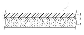
- a shield film 1 shown in FIG. 1 is obtained by sequentially providing a metal layer 3 having a thickness of 0.5 ⁇ m to 12 ⁇ m and an anisotropic conductive adhesive layer 4 on one surface of an insulating layer 2. That is, the shield film 1 includes a metal layer 3 and an anisotropic conductive adhesive layer 4 in a laminated state.
- the insulating layer 2 is made of a cover film or an insulating resin coating layer.
- the cover film is made of engineering plastic. Examples include polypropylene, crosslinked polyethylene, polyester, polybenzimidazole, aramid, polyimide, polyimideamide, polyetherimide, polyphenylene sulfide (PPS), polyethylene naphthalate (PEN), and the like.
- An inexpensive polyester film is preferable when heat resistance is not required, and a polyphenylene sulfide film is preferable when flame resistance is required, and an aramid film or a polyimide film is preferable when heat resistance is required.
- the insulating resin may be any resin having insulating properties, and examples thereof include a thermosetting resin and an ultraviolet curable resin.
- examples of the thermosetting resin include a phenol resin, an acrylic resin, an epoxy resin, a melamine resin, a silicone resin, and an acrylic modified silicone resin.
- examples of the ultraviolet curable resin include epoxy acrylate resins, polyester acrylate resins, and methacrylate-modified products thereof.
- the curing form may be any of thermosetting, ultraviolet curing, electron beam curing, etc., as long as it can be cured.
- the minimum of the thickness of the insulating layer 2 is preferably 1 ⁇ m, and more preferably 3 ⁇ m.
- the upper limit of the thickness of the insulating layer 2 is preferably 10 ⁇ m, and more preferably 7 ⁇ m.
- the metal layer 3 is formed with a thickness in the range of 0.5 ⁇ m to 12 ⁇ m. Thereby, the electric field wave, magnetic field wave, and electromagnetic wave which advance from the one surface side of the shield film to the other surface side can be well shielded, and it is also suitable when applied to a flexible printed wiring board.
- the metal layer 3 is preferably a metal foil. This makes it possible to easily obtain a metal layer having a desired layer thickness and to obtain better shielding characteristics than a thin metal layer formed by vapor deposition.
- the metal layer 3 is preferably formed by rolling. Thereby, a shield film can have favorable shape retainability. Therefore, the workability at the time of assembling the flexible substrate with the shield film bonded thereto can be improved. For example, when a flexible printed wiring board provided with a shield film is bent and assembled to a portable device or the like, the flexible printed wiring board maintains its bent state due to its good shape retention, There is no need for the operator to maintain the bent state, and the load of assembling work such as portable equipment can be reduced, and good workability can be obtained.
- the layer thickness is preferably adjusted by etching.
- the metal material forming the metal layer 3 is preferably composed mainly of copper. Thereby, since shape maintenance is excellent, while being able to obtain favorable workability and electroconductivity, a shield film can be manufactured cheaply.
- the metal layer 3 is not limited to copper as a main component, but is any one of nickel, copper, silver, tin, gold, palladium, aluminum, chromium, titanium, and zinc, or two or more of these.
- An alloy containing The metal layer 3 is not limited to a metal foil formed by rolling, but may be a metal foil by electrolysis (such as a special electrolytic copper foil) or an additive method such as vacuum deposition, sputtering, CVD, MO ( Metal organic), plating, or the like may be used.
- Plating is electrolytic plating (a method in which electricity from an external electrode or the like is used for plating through an electrolysis reaction), electroless plating (a method for plating through a chemical reaction without using electricity from an external electrode or the like)
- the metal layer 3 is more preferably 1 ⁇ m, and further preferably 2 ⁇ m.
- the upper limit of the thickness of the metal layer 3 is more preferably 6 ⁇ m, and further preferably 3 ⁇ m.
- the anisotropic conductive adhesive layer 4 is an anisotropic conductive adhesive layer having anisotropic conductivity in which an electrically conductive state is ensured only in the thickness direction.
- a flame retardant or a conductive filler is added to the adhesive to form an anisotropic conductive adhesive layer.
- the lower limit of the thickness of the anisotropic conductive adhesive layer 4 is preferably 2 ⁇ m and more preferably 3 ⁇ m. Further, the upper limit of the thickness of the anisotropic conductive adhesive layer 4 is preferably 15 ⁇ m, and more preferably 9 ⁇ m.
- the adhesive contained in the anisotropic conductive adhesive layer 4 includes, as an adhesive resin, a thermoplastic resin such as polystyrene, vinyl acetate, polyester, polyethylene, polypropylene, polyamide, rubber, and acrylic. , Phenolic, epoxy-based, urethane-based, melamine-based and alkyd-based thermosetting resins.
- the adhesive may be a single substance or a mixture of the above resins.
- the adhesive may further contain a tackifier.
- the tackifier include tackifiers such as fatty acid hydrocarbon resins, C5 / C9 mixed resins, rosin, rosin derivatives, terpene resins, aromatic hydrocarbon resins, and thermally reactive resins.
- the conductive filler added to the anisotropic conductive adhesive layer 4 is partially or entirely formed of a metal material.
- conductive fillers include copper powder, silver powder, nickel powder, silver coated copper powder (Ag coated Cu powder), gold coated copper powder, silver coated nickel powder (Ag coated Ni powder), and gold coated nickel powder.
- the metal powder can be produced by an atomizing method, a carbonyl method, or the like.
- particles obtained by coating a metal powder with a resin and particles obtained by coating a resin with a metal powder can also be used.
- one or more kinds of conductive fillers may be mixed and added to the anisotropic conductive adhesive layer 4.
- the conductive filler is preferably Ag-coated Cu powder or Ag-coated Ni powder. This is because conductive particles having stable conductivity can be obtained from an inexpensive material.
- the conductive filler is added in the range of 3 wt% to 39 wt% with respect to the total amount of the anisotropic conductive adhesive layer 4.
- the average particle size of the conductive filler is preferably in the range of 2 ⁇ m to 20 ⁇ m, but an optimal value may be selected depending on the thickness of the anisotropic conductive adhesive layer 4.
- the shape of the metal filler may be spherical, needle-like, fiber-like, flake-like, or dendritic.
- shield printed wiring board 10 (Configuration of shield printed wiring board 10)
- FPC flexible printed wiring board
- this embodiment demonstrates the case where a shield film is stuck on FPC, it is not limited to this.
- it can be used for COF (chip on flex), RF (rigid flex printed board), multilayer flexible substrate, rigid substrate and the like.
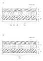
- the shield printed wiring board 10 is formed by laminating the shield film 1 and the base film (FPC) 8 described above.
- the base film 8 is formed by sequentially laminating a base film 5, a printed circuit 6, and an insulating film 7.
- the surface of the printed circuit 6 includes a signal circuit 6a and a ground circuit 6b, and is covered with an insulating film 7 except for at least a part (non-insulating portion 6c) of the ground circuit 6b.
- the insulating film 7 has the insulation removal part 7a into which a part of anisotropic conductive adhesive layer 4 of the shield film 1 flows in the inside. Thereby, the ground circuit 6b and the metal layer 3 are electrically connected.
- the signal circuit 6a and the ground circuit 6b are formed with a wiring pattern by etching the conductive material.
- the ground circuit 6b refers to a pattern that maintains the ground potential. That is, the base film 5 is formed with a ground circuit 6b which is a ground wiring pattern. As shown in FIG. 2B, the printed circuit 6 may not include the ground circuit 6b. In this case, the printed circuit 6 is covered with the insulating film 7.
- a signal having a frequency of 10 MHz to 10 GHz is transmitted to the signal circuit 6a. That is, the shield film 1 is preferably applied as a shield film for a signal transmission system in which a signal having a frequency of 10 MHz to 10 GHz is transmitted, but is not limited thereto.
- the lower limit of the frequency of the signal transmission system to which the shield film 1 is applied is preferably 10 MHz, and more preferably 100 MHz.
- the upper limit of the frequency of the signal transmission system to which the shield film 1 is applied is preferably 10 GHz, and more preferably 5 GHz.
- the base film 5 and the printed circuit 6 may be joined together by an adhesive, or may be joined in the same manner as a so-called adhesiveless copper-clad laminate that does not use an adhesive.
- the insulating film 7 may be formed by bonding a flexible insulating film using an adhesive, or by a series of techniques such as application of a photosensitive insulating resin, drying, exposure, development, and heat treatment. . When the insulating film 7 is pasted using an adhesive, the insulating removal portion 7a is also formed at the location of the ground circuit 6b of the adhesive.
- the base film 8 is a single-sided FPC having a printed circuit only on one side of the base film, a double-sided FPC having a printed circuit on both sides of the base film, and a multilayer in which a plurality of such FPCs are laminated.
- FPC Flexboard (registered trademark) with multi-layer component mounting part and cable part, flex-rigid board with rigid members constituting multi-layer part, or TAB tape for tape carrier package Can be implemented.
- the base film 5 and the insulating film 7 are both made of engineering plastic. Examples thereof include resins such as polyethylene terephthalate, polypropylene, crosslinked polyethylene, polyester, polybenzimidazole, polyimide, polyimide amide, polyether imide, and polyphenylene sulfide (PPS).
- resins such as polyethylene terephthalate, polypropylene, crosslinked polyethylene, polyester, polybenzimidazole, polyimide, polyimide amide, polyether imide, and polyphenylene sulfide (PPS).
- PPS polyphenylene sulfide
- An inexpensive polyester film is preferable when heat resistance is not required, and a polyphenylene sulfide film is preferable when flame resistance is required, and a polyimide film is preferable when heat resistance is required.
- 10 micrometers is preferable and the minimum of the thickness of the base film 5 has more preferable 20 micrometers.
- the upper limit of the thickness of the base film 5 is preferably 60 ⁇ m, and more preferably 40 ⁇ m.
- the lower limit of the thickness of the insulating film 7 is preferably 10 ⁇ m, and more preferably 20 ⁇ m.
- the upper limit of the thickness of the insulating film 7 is preferably 60 ⁇ m, and more preferably 40 ⁇ m.
- the manufacturing method of the shield film 1 of this embodiment is demonstrated. First, rolling is performed through copper between rotating rolls to reduce the thickness to the first dimension.
- the lower limit of the thickness of the first dimension is preferably 3 ⁇ m, more preferably 6 ⁇ m, and even more preferably 9 ⁇ m.
- the upper limit of the thickness of the first dimension is preferably 35 ⁇ m, more preferably 18 ⁇ m, and further preferably 12 ⁇ m.
- etching is performed on the copper foil that has been rolled to have the first dimension, and the metal layer 3 is formed by reducing the thickness to the second dimension (0.5 ⁇ m to 12 ⁇ m).
- ⁇ m of copper foil is dipped in an etching solution of sulfuric acid and hydrogen peroxide to be processed to a thickness of 2 ⁇ m.
- an anisotropic conductive adhesive layer 4 is coated on one surface of the metal layer 3.
- the insulating layer 2 which is a protective film is stuck on the other surface of the formed metal layer 3. Note that the step of forming the insulating layer can be omitted.
- the insulating film 7 of the base film 8 is perforated by laser processing or the like to form the insulating removal portion 7a.
- the shield film 1 is bonded onto the insulating film 7 of the base film 8.
- the printed wiring board 10 and the shield film 1 are pressure-bonded from above and below by a press machine while the shield film 1 is heated by a heater.
- the anisotropic conductive adhesive layer 4 of the shield film 1 is softened by the heat of the heater, and is adhered onto the insulating film 7 by pressurization of a press.
- the anisotropically conductive adhesive layer 4 that has become soft is filled in the insulation removal portion 7a. Therefore, it adheres to the anisotropic conductive adhesive layer 4 filled with a part of the ground circuit 6b exposed at the insulation removal portion 7a. As a result, the ground circuit 6 b and the metal layer 3 are electrically connected via the anisotropic conductive adhesive layer 4.
- the shield film 1 is attached to one side, but is not limited thereto.
- a shield film may be attached to both sides.
- the shield printed wiring board 10 when copper is used as the metal material for forming the metal layer 3, the surface of the metal layer 3 is oxidized due to the influence of manufacturing conditions and manufacturing processes, and the surface resistance is increased. May end up.
- the surface resistance increases in this way, the connection resistance from the anisotropic conductive adhesive layer 4 to the ground circuit 6b also increases, and as a result, the shielding effect of the shield film 1 may be reduced. Therefore, as shown in FIG. 11, a protective metal layer 3 a having a low surface resistance / contact resistance may be provided between the metal layer 3 and the anisotropic conductive adhesive layer 4. In this case, it is preferable to use silver (Ag) or gold (Au) for the protective metal layer 3a.
- the protective metal layer 3a as in the method for forming the metal layer 3, there are methods such as vacuum deposition, sputtering, CVD, MO (metal organic), plating, which are additive methods.
- vacuum deposition sputtering, CVD, MO (metal organic), plating, which are additive methods.
- MO metal organic
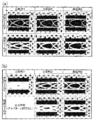
- the shield film (measurement sample) 101 shown in Table 1 was used.
- Table 1 shows the manufacturing method and material of the metal layer, and whether the adhesive layer is an anisotropic conductive adhesive or an isotropic conductive adhesive.
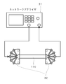
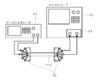
- the electromagnetic wave shielding effect measuring device 11 (electric field wave shielding effect evaluation device 11a, magnetic field wave shielding effect evaluation device 11b) developed at the KEC Kansai Electronics Industry Promotion Center with respect to the electric field wave and magnetic field shielding properties of the shield film. It was evaluated by the KEC method using FIG. 3 is a diagram showing the configuration of a system used in the KEC method.
- the system used in the KEC method includes an electromagnetic wave shielding effect measuring device 11, a spectrum analyzer 21, an attenuator 22 that attenuates 10 dB, an attenuator 23 that attenuates 3 dB, and a preamplifier 24.
- HP 8447F manufactured by Agilent Technologies was used.
- FIG. 3A shows the electric field wave shield effect evaluation apparatus 11a
- FIG. 3B shows the magnetic field wave shield effect evaluation apparatus 11b.
- the electric field wave shield effect evaluation device 11a is provided with two measuring jigs 13 facing each other.
- the measurement target shield film (measurement sample) 101 shown in Table 1 is installed between the measurement jigs 13 and 13 so as to be sandwiched therebetween.
- the measurement jig 13 adopts a TEM cell (Transverse ElectroMagnetic Cell) size distribution and has a structure in which the measurement jig 13 is symmetrically divided in a plane perpendicular to the transmission axis direction. However, in order to prevent a short circuit from being formed due to the insertion of the measurement sample 101, the flat central conductor 14 is arranged with a gap between each measurement jig 13.
- the electric field wave shield effect evaluation apparatus 11a is provided with two measuring jigs 15 facing each other. The shield film 101 to be measured is installed so as to be sandwiched between the measurement jigs 15 and 15.
- the magnetic field shield effect evaluation apparatus 11b uses a shielded circular loop antenna 16 as a measurement jig 15, and combines it with a 90 ° square metal plate.
- the structure is such that a quarter of the antenna is exposed to the outside.
- Example 3 Example 5 shown in Table 1, and the shielding film 101 of the comparative example 1, it measured using what was cut
- measurement was performed in a frequency range of 1 MHz to 1 GHz. The measurement was performed in an atmosphere at a temperature of 25 ° C. and a relative humidity of 30 to 50%.
- a signal output from the spectrum analyzer 21 is input to the measurement jig 13 or the measurement jig 15 on the transmission side via the attenuator 22. Then, the signal is received by the measuring jig 13 or the measuring jig 15 on the receiving side and the signal via the attenuator 23 is amplified by the preamplifier 24, and then the signal level is measured by the spectrum analyzer 21.
- the spectrum analyzer 21 outputs the attenuation when the shield film is installed in the electromagnetic wave shielding effect measuring device 11 with reference to the state where the shield film is not installed in the electromagnetic wave shielding effect measuring device 11.
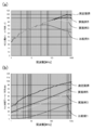
- the measurement result of the electric field wave shielding performance by the KEC method is shown in FIG. 4A, and the measurement result of the magnetic field wave shielding performance is shown in FIG. 4B.
- the attenuation of Examples 3 and 5 is larger than that of Comparative Example 1 and is effective as a shield characteristic.
- the frequency characteristics of the shield film were evaluated using a network analyzer 31 as shown in FIG.
- the network analyzer 31 ZVL6 manufactured by Rohde & Schwarz was used.
- the network analyzer 31 has an input terminal and an output terminal, and a connection board 32 is connected to each of them.
- the measurement is performed by connecting the shield flexible printed wiring board 110 to be measured so as to be supported in a straight state floating in the air between the pair of connection boards 32.
- 110 was fabricated (hereinafter referred to as a single-sided shield) as a measurement target (shielded flexible printed wiring board 110a).
- the object to be measured hereinafter referred to as a double-sided shield manufactured by attaching the shield film 101 to the base film side of the shield flexible printed wiring board 110a was also set as a measurement target (shield flexible printed wiring board 110b).
- shield flexible printed wiring boards 110 a 37.5 ⁇ m insulating film in which a 12.5 ⁇ m thick polyimide film and a 25 ⁇ m thick adhesive layer were combined was used.
- the circuit pattern used was a 12 ⁇ m copper foil plated with 6 ⁇ m copper. As described above, the circuit pattern does not include a ground circuit. Further, a 25 ⁇ m polyimide film was used as the base film. Further, the shield flexible printed wiring board 110 having a length of 200 mm was used. Further, the measurement was performed in the frequency range of 100 kHz to 6 GHz. The measurement was performed in an atmosphere at a temperature of 25 ° C. and a relative humidity of 30 to 50%.
- the network analyzer 31 measures for each frequency how much the input signal is attenuated with respect to the output signal.
- the measurement result of the single-sided shield by the network analyzer 31 is shown in FIG. 6A, and the measurement result of the double-sided shield is shown in FIG. 6B. From this, it was found that in both the single-sided shield and the double-sided shield, the attenuation amount of Example 5 was lower than that of Comparative Examples 1 and 2 and had good transmission characteristics.
- Table 2 shows attenuation amounts at typical frequencies in Comparative Examples 1 and 2 and Example 5.
- the shield film of the present invention is applied as a shield film for a signal transmission system that transmits a signal having a frequency of 10 MHz to 10 GHz, so that an electric field wave and a magnetic field wave traveling from one surface side to the other surface side of the shield film.
- electromagnetic waves can be well shielded.
- FIG. 1 This system includes a data generator 41, an oscilloscope 42, a sampling module 43 attached to the oscilloscope 42, and a pair of connection boards 32.
- the data generator 41 81133A manufactured by Agilent Technologies was used.
- the oscilloscope 42 DSC8200 manufactured by Tektronix was used.
- the sampling module 43 80E03 manufactured by Tektronix was used.
- connection board 32 has an input terminal and an output terminal, and the shielded flexible printed wiring board 110 to be measured is floated in the air between the pair of connection boards 32.
- the eye pattern is observed by connecting to the data generator 41 and the sampling module 43.
- the input amplitude was 150 mV / side (300 mVdiff).
- the data pattern was PRBS23. The measurement was performed in an atmosphere at a temperature of 25 ° C. and a relative humidity of 30 to 50%.
- FIG. 8A shows the measurement results observed with the oscilloscope 42 when the bit rate is 1.0 Gbps
- FIG. 8B shows the measurement results when the bit rate is 3.0 Gbps.
- the eye pattern of Comparative Examples 1 and 2 has more jitter than Example 5 regardless of single-sided shield or double-sided shield, and Example 5 is faster. It was found to be suitable for.
- the shape retention of the shield film was evaluated.
- the test body 51 was obtained by bonding the shield film 101 shown in Table 1 on both sides of a 50 ⁇ m polyimide film.
- the test body 51 was cut into a shape of 10 mm ⁇ 100 mm. As shown in FIG. 9, such a test body 51 is bent so as to be slightly creased at a bent portion 51a near the center in the longitudinal direction (around 50 mm), and an upper portion 51b and a lower portion 51c divided by the bent portion 51a. Are in such a manner that they face each other.
- the entire test body 51 is placed on a PP (polypropylene) substrate 54 and 0.3 mm thick as spacers on both sides of the test body 51 so as to be parallel to the longitudinal direction of the test body 51.
- a SUS plate (not shown) was arranged. Then, the silicon rubber 53 was lowered from above, and the entire test body 51 was pressed together with the SUS plate. That is, since there is a 0.3 mm SUS plate, the bending radius at the bent portion 51 a of the test body 51 is 0.15 mm.
- the pressurizing time is set to 1 second, 3 seconds, and 5 seconds in both cases where the pressure applied by the press is 0.1 MPa and 0.3 MPa, and the upper part 51b and the lower part 51c form the test body 51 after pressing.
- the angle (return angle) was measured.
- Table 3 to be described later shows the results of measuring the return angle for Examples 1 to 5 and Comparative Examples 1 and 2. Evaluation was made with double-sided sticking, with an angle of 90 degrees or less marked with ⁇ , and with more than 120 degrees marked with x. According to Table 3, it can be seen that the rolled copper foil has better shape retention. That is, it can be seen that the rolled copper foil is effective for shape retention.
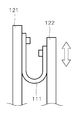
- a shielded flexible printed wiring board 111 (any one of the samples of Examples 1 to 5 and Comparative Examples 1 and 2 described above) is used between the fixed plate 121 and the sliding plate 122. Is bent in a U shape with a curvature of 0.65 mm and a gap between the fixed plate 121 and the sliding plate 122 of 1.30 mm. Resistance of the metal layer of the shield film in the shield flexible printed wiring board when the sliding plate 122 is slid up and down at a stroke of 50 mm (sliding area 25 mm) and a sliding speed of 60 cpm at a humidity of 30 to 50% (what It can be verified whether it can withstand a single slide. Each shield film had a length of 140 mm. The verification results of Examples 1 to 5 and Comparative Examples 1 and 2 are shown in Table 3 below together with shape retention.
- Table 3 also shows the verification results of Examples 1 to 5 and Comparative Examples 1 and 2 regarding the above-described frequency characteristics and shield characteristics.
- the frequency characteristics are shown for the frequency when the attenuation is ⁇ 3 dB and ⁇ 10 dB.
- the shield characteristic the attenuation amount with respect to the electric field wave at 1 GHz is shown.
- the slidability is extremely lowered when the metal layer exceeds 5 ⁇ m. Therefore, when the slidability is required, it is clear that the metal layer is preferably 5 ⁇ m or less.
- shape retention it can be seen that good shape retention is obtained when the metal layer is made of copper foil and formed by rolling. Therefore, it is clear that it is preferable to use a rolled copper foil when shape retention is required.
- connection resistance ⁇ Connection resistance> Next, it measured about the connection resistance of the shield film and shield printed wiring board which passed through the manufacturing process which manufactures the shield printed wiring board 10 (measurement of the connection resistance after reflow). Specifically, as shown in Table 4, in Example 6, the copper foil was not subjected to rust prevention treatment, and the silver film between the metal layer 3 of the shield film 1 and the anisotropic conductive adhesive layer 4 was silver-coated. Was used to measure the connection resistance value ( ⁇ ) between the shield film 1 and the ground circuit 6b using the shield printed wiring board 10 provided with the protective metal layer 3a having a thickness of 0.05 ⁇ m.
- Example 7 the copper foil was not subjected to rust prevention treatment, and silver was vacuum-deposited between the metal layer 3 and the anisotropic conductive adhesive layer 4 of the shield film 1 to a thickness of 0.1 ⁇ m.
- the connection resistance value ( ⁇ ) between the shield film 1 and the ground circuit 6b was measured.
- the copper foil was not subjected to rust prevention treatment, and silver was plated between the metal layer 3 and the anisotropic conductive adhesive layer 4 of the shield film 1 to a thickness of 0.05 ⁇ m.
- the shield printed wiring board 10 provided with the protective metal layer 3a the connection resistance value ( ⁇ ) between the shield film 1 and the ground circuit 6b was measured.
- Example 9 the copper foil was not subjected to rust prevention treatment, and silver was plated between the metal layer 3 and the anisotropic conductive adhesive layer 4 of the shield film 1 to a thickness of 0.1 ⁇ m.
- the connection resistance value ( ⁇ ) between the shield film 1 and the ground circuit 6b was measured.
- the connection resistance value ((ohm)) between the shield film 1 and the ground circuit 6b in the shield printed wiring board which performed a rust prevention process as a process of copper foil, and does not provide the protective metal layer 3a was measured. .
- the insulating layer 2 has a thickness of 5 ⁇ m
- the metal layer 3 (rolled copper foil) has a thickness of 6 ⁇ m
- the anisotropic conductive adhesive layer 4 has a thickness of 9 ⁇ m.
- the shield films 1 of Examples 6 to 9 have a configuration in which a protective metal layer 3a is further provided between the metal layer 3 and the anisotropic conductive adhesive layer 4.
- connection resistance of Example 5 is 2 ⁇ or less, it is a level that can withstand practical use.
- Example 6 and Example 8 and Example 7 and Example 9 are compared, as a formation method of the protective metal layer 3a, the connection resistance is smaller when formed by plating than by vacuum deposition. I understand.
- Example 6 and Example 7 and Example 8 and Example 9 are compared, it turns out that the one where the protective metal layer 3a is thick has a small connection resistance.
Landscapes
- Engineering & Computer Science (AREA)
- Microelectronics & Electronic Packaging (AREA)
- Physics & Mathematics (AREA)
- Electromagnetism (AREA)
- Shielding Devices Or Components To Electric Or Magnetic Fields (AREA)
- Laminated Bodies (AREA)
- Structure Of Printed Boards (AREA)
- Manufacturing Of Electric Cables (AREA)
- Other Surface Treatments For Metallic Materials (AREA)
- Non-Insulated Conductors (AREA)
- Manufacturing & Machinery (AREA)
Priority Applications (4)
| Application Number | Priority Date | Filing Date | Title |
|---|---|---|---|
| US14/360,609 US10015915B2 (en) | 2011-11-24 | 2012-10-12 | Shield film, shielded printed wiring board, and method for manufacturing shield film |
| KR20147014926A KR20140099258A (ko) | 2011-11-24 | 2012-10-12 | 차폐 필름, 차폐 프린트 배선판, 및 차폐 필름의 제조 방법 |
| KR1020197026802A KR20190107768A (ko) | 2011-11-24 | 2012-10-12 | 차폐 필름, 차폐 프린트 배선판, 및 차폐 필름의 제조 방법 |
| US15/019,775 US10051765B2 (en) | 2011-11-24 | 2016-02-09 | Shield film, shielded printed wiring board, and method for manufacturing shield film |
Applications Claiming Priority (2)
| Application Number | Priority Date | Filing Date | Title |
|---|---|---|---|
| JP2011256816 | 2011-11-24 | ||
| JP2011-256816 | 2011-11-24 |
Related Child Applications (2)
| Application Number | Title | Priority Date | Filing Date |
|---|---|---|---|
| US14/360,609 A-371-Of-International US10015915B2 (en) | 2011-11-24 | 2012-10-12 | Shield film, shielded printed wiring board, and method for manufacturing shield film |
| US15/019,775 Continuation US10051765B2 (en) | 2011-11-24 | 2016-02-09 | Shield film, shielded printed wiring board, and method for manufacturing shield film |
Publications (1)
| Publication Number | Publication Date |
|---|---|
| WO2013077108A1 true WO2013077108A1 (ja) | 2013-05-30 |
Family
ID=48469561
Family Applications (1)
| Application Number | Title | Priority Date | Filing Date |
|---|---|---|---|
| PCT/JP2012/076473 WO2013077108A1 (ja) | 2011-11-24 | 2012-10-12 | シールドフィルム、シールドプリント配線板、及び、シールドフィルムの製造方法 |
Country Status (6)
Cited By (16)
| Publication number | Priority date | Publication date | Assignee | Title |
|---|---|---|---|---|
| JP2014241330A (ja) * | 2013-06-11 | 2014-12-25 | 住友電工プリントサーキット株式会社 | シールドフィルム及びプリント配線板 |
| JP2015065343A (ja) * | 2013-09-25 | 2015-04-09 | タツタ電線株式会社 | シールド収容体、プリント回路板、電子機器、及び、シールド収容体の製造方法 |
| JP2016157838A (ja) * | 2015-02-25 | 2016-09-01 | 東洋インキScホールディングス株式会社 | 電磁波シールドシート、電磁波シールド性配線回路基板および電子機器 |
| WO2016190278A1 (ja) * | 2015-05-26 | 2016-12-01 | タツタ電線株式会社 | シールドフィルムおよびシールドプリント配線板 |
| US10015915B2 (en) | 2011-11-24 | 2018-07-03 | Tatsuta Electric Wire & Cable Co., Ltd. | Shield film, shielded printed wiring board, and method for manufacturing shield film |
| KR20190073037A (ko) * | 2017-12-18 | 2019-06-26 | 주식회사 잉크테크 | 전자파 차폐필름, 인쇄회로기판 제조방법 및 전자파 차폐필름 제조방법 |
| JP2020080345A (ja) * | 2018-11-12 | 2020-05-28 | 信越ポリマー株式会社 | 電磁波シールドフィルムおよび電磁波シールドフィルム付きプリント配線板 |
| JP2020167250A (ja) * | 2019-03-29 | 2020-10-08 | 東洋インキScホールディングス株式会社 | 電磁波シールドシート、電磁波シールド性配線回路基板および電子機器 |
| US10820457B1 (en) | 2019-05-30 | 2020-10-27 | Toyo Ink Sc Holdings Co., Ltd. | Electromagnetic wave shielding sheet and printed wiring board |
| KR20200144492A (ko) | 2019-06-18 | 2020-12-29 | 토요잉크Sc홀딩스주식회사 | 전자파 차폐 시트, 및 전자파 차폐성 배선 회로 기판 |
| KR102238608B1 (ko) | 2019-12-18 | 2021-04-09 | 토요잉크Sc홀딩스주식회사 | 전자파 차폐 시트 및 전자파 차폐성 배선 회로 기판 |
| KR102238611B1 (ko) | 2020-01-21 | 2021-04-09 | 토요잉크Sc홀딩스주식회사 | 전자파 차폐 시트 및 전자파 차폐성 배선 회로 기판 |
| KR20210142643A (ko) | 2019-03-22 | 2021-11-25 | 타츠타 전선 주식회사 | 전자파 차폐 필름 |
| KR20240167785A (ko) | 2022-03-29 | 2024-11-28 | 타츠타 전선 주식회사 | 전자파 실드 필름 |
| KR20250088703A (ko) | 2022-10-12 | 2025-06-17 | 타츠타 전선 주식회사 | 전자파 차폐 필름 및 차폐 프린트 배선판 |
| KR20250119519A (ko) | 2022-12-02 | 2025-08-07 | 타츠타 전선 주식회사 | 전자파 차폐 필름 및 전자파 차폐 필름의 제조 방법 |
Families Citing this family (39)
| Publication number | Priority date | Publication date | Assignee | Title |
|---|---|---|---|---|
| JP6368711B2 (ja) * | 2013-05-28 | 2018-08-01 | タツタ電線株式会社 | 形状保持シールドフィルム、及びこの形状保持シールドフィルムを備えた形状保持型シールドフレキシブル配線板 |
| TWI573498B (zh) * | 2013-07-26 | 2017-03-01 | Adv Flexible Circuits Co Ltd | The flattened cladding structure of soft circuit board |
| CN104582240B (zh) * | 2013-10-25 | 2017-08-25 | 富葵精密组件(深圳)有限公司 | 电路板及电路板制作方法 |
| US9345181B2 (en) * | 2014-08-19 | 2016-05-17 | T-Kingdom Co., Ltd. | Shielding film and method of manufacturing same |
| JP6781631B2 (ja) * | 2014-08-29 | 2020-11-04 | タツタ電線株式会社 | フレキシブルプリント配線板用補強部材、及びそれを備えたフレキシブルプリント配線板 |
| JP6184025B2 (ja) * | 2014-09-04 | 2017-08-23 | 信越ポリマー株式会社 | 電磁波シールドフィルムおよび電磁波シールドフィルム付きフレキシブルプリント配線板の製造方法 |
| JP6467701B2 (ja) * | 2014-10-28 | 2019-02-13 | 信越ポリマー株式会社 | 電磁波シールドフィルム、電磁波シールドフィルム付きフレキシブルプリント配線板、およびそれらの製造方法 |
| JP2016092053A (ja) * | 2014-10-30 | 2016-05-23 | 京セラサーキットソリューションズ株式会社 | 配線基板 |
| JP6461577B2 (ja) * | 2014-11-28 | 2019-01-30 | 東洋アルミニウム株式会社 | Rfid用インレットアンテナ及びrfid並びにそれらの製造方法 |
| US10665568B2 (en) * | 2014-12-12 | 2020-05-26 | Meiko Electronics Co., Ltd. | Encapsulated circuit module, and production method therefor |
| CN105828587A (zh) * | 2015-01-06 | 2016-08-03 | 富葵精密组件(深圳)有限公司 | 感光油墨及应用其的电磁屏蔽结构、电路板、电子装置 |
| CN105139922A (zh) * | 2015-09-21 | 2015-12-09 | 杨天纬 | 一种用于线缆的屏蔽膜及制造方法及线材的制造方法 |
| CN105139923A (zh) * | 2015-09-21 | 2015-12-09 | 杨天纬 | 一种用于线缆的屏蔽膜及制造方法及线材的制造方法 |
| KR102280175B1 (ko) * | 2016-03-23 | 2021-07-20 | 타츠타 전선 주식회사 | 전자파 차폐 필름 |
| CN107234803B (zh) * | 2016-03-28 | 2019-08-30 | 努比亚技术有限公司 | 一种粘贴保护膜时的处理系统和方法 |
| KR102520709B1 (ko) | 2016-04-19 | 2023-04-12 | 삼성디스플레이 주식회사 | 인쇄회로기판용 보호테이프 및 이를 구비하는 디스플레이 장치 |
| KR20170123747A (ko) * | 2016-04-29 | 2017-11-09 | 삼성전자주식회사 | 차폐 부재 및 그를 포함하는 전자 장치 |
| JP2018010888A (ja) * | 2016-07-11 | 2018-01-18 | 藤森工業株式会社 | 電磁波シールド材 |
| CN106061103A (zh) * | 2016-07-21 | 2016-10-26 | 东莞市航晨纳米材料有限公司 | 一种高柔软性电磁屏蔽膜及其制造方法 |
| CN107914435B (zh) * | 2016-10-10 | 2019-10-29 | 昆山雅森电子材料科技有限公司 | 一种多层异向导电胶膜及其制作方法 |
| CN110235530A (zh) * | 2017-02-13 | 2019-09-13 | 拓自达电线株式会社 | 印制线路板 |
| KR102467723B1 (ko) * | 2017-02-13 | 2022-11-16 | 타츠타 전선 주식회사 | 그라운드 부재, 차폐 프린트 배선판 및 차폐 프린트 배선판의 제조 방법 |
| US10080277B1 (en) * | 2017-03-17 | 2018-09-18 | Advanced Flexible Circuits Co., Ltd. | Attenuation reduction structure for flexible circuit board |
| TWI658753B (zh) * | 2017-03-17 | 2019-05-01 | 易鼎股份有限公司 | Signal anti-attenuation shielding structure of flexible circuit board |
| KR101966230B1 (ko) * | 2017-03-24 | 2019-04-30 | (주)창성 | 롤투롤 공정을 이용한 fpcb용 다층 전자파 차폐 필름 제조방법 |
| US10159143B1 (en) * | 2017-07-31 | 2018-12-18 | Advanced Flexible Circuits Co., Ltd. | Attenuation reduction structure for flexible circuit board |
| EP3468312B1 (en) * | 2017-10-06 | 2023-11-29 | AT & S Austria Technologie & Systemtechnik Aktiengesellschaft | Method of manufacturing a component carrier having a three dimensionally printed wiring structure |
| FR3074400B1 (fr) * | 2017-11-30 | 2019-10-25 | Safran Electronics & Defense | Circuit imprime flexible avec piste de masse intermediaire |
| KR102607345B1 (ko) * | 2018-12-11 | 2023-11-27 | 타츠타 전선 주식회사 | 차폐 프린트 배선판의 제조 방법 및 차폐 프린트 배선판 |
| KR102843874B1 (ko) * | 2019-04-09 | 2025-08-08 | 삼성전자주식회사 | 연성 인쇄 회로 기판 및 그 연성 인쇄 회로 기판을 포함하는 전자 장치 |
| CN113853839B (zh) * | 2019-05-29 | 2022-09-30 | 拓自达电线株式会社 | 电磁波屏蔽膜及屏蔽印制线路板 |
| CN112771598B (zh) * | 2019-08-01 | 2023-09-29 | 京东方科技集团股份有限公司 | 显示装置及其组装方法 |
| JP6624331B1 (ja) * | 2019-08-01 | 2019-12-25 | 東洋インキScホールディングス株式会社 | 電磁波シールドシート、および電磁波シールド性配線回路基板 |
| KR102705794B1 (ko) * | 2019-08-05 | 2024-09-12 | 삼성전자 주식회사 | 차폐 필름을 포함하는 플렉서블 케이블 |
| TWI829973B (zh) * | 2020-02-25 | 2024-01-21 | 日商拓自達電線股份有限公司 | 電磁波屏蔽膜 |
| CN111465175B (zh) * | 2020-04-23 | 2022-08-12 | 京东方科技集团股份有限公司 | 电路板及其制备方法、电子设备 |
| JP2022170878A (ja) * | 2021-04-30 | 2022-11-11 | 株式会社コバヤシ | めっき用プライマー組成物 |
| TW202313327A (zh) * | 2021-09-29 | 2023-04-01 | 日商拓自達電線股份有限公司 | 電磁波屏蔽膜 |
| US11747295B2 (en) * | 2021-10-18 | 2023-09-05 | Dell Products L.P. | System and method of determining humidity levels within information handling systems |
Citations (4)
| Publication number | Priority date | Publication date | Assignee | Title |
|---|---|---|---|---|
| JP2007294918A (ja) * | 2006-03-29 | 2007-11-08 | Tatsuta System Electronics Kk | シールドフィルム及びシールドプリント配線板 |
| JP2008120081A (ja) * | 2006-11-11 | 2008-05-29 | Joinset Co Ltd | 軟性金属積層フィルム及びその製造方法 |
| JP2009200113A (ja) * | 2008-02-19 | 2009-09-03 | Nitto Denko Corp | シールド配線回路基板 |
| JP2009206188A (ja) * | 2008-02-26 | 2009-09-10 | Panasonic Electric Works Co Ltd | フレキシブルプリント配線板 |
Family Cites Families (29)
| Publication number | Priority date | Publication date | Assignee | Title |
|---|---|---|---|---|
| JP3498386B2 (ja) | 1994-10-19 | 2004-02-16 | 住友電気工業株式会社 | シールド付きフレキシブル配線板及びその製造方法 |
| JP2000013089A (ja) | 1998-06-25 | 2000-01-14 | Tomoegawa Paper Co Ltd | ディスプレイ用電磁波シールド材 |
| JP2000059075A (ja) | 1998-08-10 | 2000-02-25 | Sumitomo Bakelite Co Ltd | 電磁波遮蔽透明体 |
| SG81995A1 (en) | 1998-08-10 | 2001-07-24 | Sumitomo Bakelite Co | Transparent electromagnetic wave shield |
| KR100910188B1 (ko) | 2001-07-19 | 2009-07-30 | 도레이 카부시키가이샤 | 회로기판, 회로기판용 부재 및 그 제조방법 및가요성필름의 라미네이트방법 |
| ATE528924T1 (de) * | 2001-11-22 | 2011-10-15 | Panasonic Corp | Kodierungs- und dekodierungsverfahren variabler länge |
| JP4156233B2 (ja) | 2001-12-19 | 2008-09-24 | 大日本印刷株式会社 | 電磁波シールド材、及び電磁波シールド付きフラットケーブル |
| JP2008300881A (ja) | 2002-02-05 | 2008-12-11 | Toray Ind Inc | 回路基板用部材およびそれを用いた電子部品実装回路基板の製造方法 |
| JP4330868B2 (ja) | 2002-11-27 | 2009-09-16 | タツタ電線株式会社 | プリント配線板およびその製造方法 |
| JP2005235509A (ja) * | 2004-02-18 | 2005-09-02 | Jsr Corp | 異方導電性シートおよび回路装置の検査装置並びに回路装置の検査方法 |
| JP4647924B2 (ja) | 2004-03-23 | 2011-03-09 | タツタ電線株式会社 | プリント配線板用シールドフィルム及びその製造方法 |
| JP2005277262A (ja) * | 2004-03-26 | 2005-10-06 | Toray Ind Inc | 電磁波シールドフィルム |
| WO2006059771A1 (ja) | 2004-12-03 | 2006-06-08 | Nitta Corporation | 電磁干渉抑制体、アンテナ装置、及び電子情報伝達装置 |
| JP4575189B2 (ja) | 2005-02-21 | 2010-11-04 | タツタ電線株式会社 | シールドフレキシブルプリント配線板のシールドフィルム及びそれを用いたシールドフレキシブルプリント配線板 |
| JP2006303067A (ja) | 2005-04-19 | 2006-11-02 | Nippon Jitsupaa Chiyuubingu Kk | 発塵防止型導電性シート及びその製造方法 |
| JP4319167B2 (ja) * | 2005-05-13 | 2009-08-26 | タツタ システム・エレクトロニクス株式会社 | シールドフィルム、シールドプリント配線板、シールドフレキシブルプリント配線板、シールドフィルムの製造方法及びシールドプリント配線板の製造方法 |
| EP1962569A1 (en) | 2005-12-16 | 2008-08-27 | Ibiden Co., Ltd. | Multilayer printed wiring plate, and method for fabricating the same |
| JP2007193999A (ja) | 2006-01-17 | 2007-08-02 | Sony Chemical & Information Device Corp | 伝送ケーブル |
| WO2007119513A1 (ja) | 2006-03-29 | 2007-10-25 | Tatsuta System Electronics Co., Ltd. | シールドフィルム及びシールドプリント配線板 |
| JP4974803B2 (ja) | 2007-08-03 | 2012-07-11 | タツタ電線株式会社 | プリント配線板用シールドフィルム及びプリント配線板 |
| JP5213106B2 (ja) | 2008-01-17 | 2013-06-19 | デクセリアルズ株式会社 | フラットケーブル |
| JP2009177010A (ja) * | 2008-01-25 | 2009-08-06 | Toshiba Corp | フレキシブルプリント配線板および電子機器 |
| JP2009246121A (ja) | 2008-03-31 | 2009-10-22 | Nippon Steel Chem Co Ltd | 電磁波シールド材及びその製造方法 |
| JP5139156B2 (ja) | 2008-05-30 | 2013-02-06 | タツタ電線株式会社 | 電磁波シールド材及びプリント配線板 |
| JP2010108779A (ja) | 2008-10-30 | 2010-05-13 | Sony Chemical & Information Device Corp | シールド材及びその製造方法、フレキシブルフラットケーブル及びその製造方法、並びに、電子機器 |
| JP2011066329A (ja) | 2009-09-18 | 2011-03-31 | Tatsuta Electric Wire & Cable Co Ltd | シールドフィルム、そのシールドフィルムを有するシールド配線板、シールドフィルムにおけるグランド接続方法 |
| US20130068521A1 (en) * | 2010-03-05 | 2013-03-21 | Sungkyunkwan University Foundation For Corporate Collaboration | Electromagnetic shielding method using graphene and electromagnetic shiedling material |
| CN102387656B (zh) * | 2010-08-30 | 2013-10-09 | 富葵精密组件(深圳)有限公司 | 具有接地屏蔽结构的电路板及其制作方法 |
| WO2013077108A1 (ja) | 2011-11-24 | 2013-05-30 | タツタ電線株式会社 | シールドフィルム、シールドプリント配線板、及び、シールドフィルムの製造方法 |
-
2012
- 2012-10-12 WO PCT/JP2012/076473 patent/WO2013077108A1/ja active Application Filing
- 2012-10-12 JP JP2013545845A patent/JPWO2013077108A1/ja active Pending
- 2012-10-12 US US14/360,609 patent/US10015915B2/en active Active
- 2012-10-12 KR KR1020197026802A patent/KR20190107768A/ko not_active Ceased
- 2012-10-12 KR KR20147014926A patent/KR20140099258A/ko not_active Ceased
- 2012-10-19 TW TW101138571A patent/TWI596998B/zh active
- 2012-11-08 CN CN2012205866628U patent/CN203225988U/zh not_active Expired - Lifetime
- 2012-11-08 CN CN201210443949XA patent/CN103140126A/zh active Pending
-
2014
- 2014-12-18 JP JP2014256256A patent/JP6321535B2/ja active Active
-
2015
- 2015-10-23 JP JP2015208837A patent/JP2016040837A/ja active Pending
- 2015-10-23 JP JP2015208838A patent/JP2016036044A/ja active Pending
-
2016
- 2016-02-09 US US15/019,775 patent/US10051765B2/en active Active
-
2019
- 2019-02-12 JP JP2019022389A patent/JP2019083205A/ja active Pending
Patent Citations (4)
| Publication number | Priority date | Publication date | Assignee | Title |
|---|---|---|---|---|
| JP2007294918A (ja) * | 2006-03-29 | 2007-11-08 | Tatsuta System Electronics Kk | シールドフィルム及びシールドプリント配線板 |
| JP2008120081A (ja) * | 2006-11-11 | 2008-05-29 | Joinset Co Ltd | 軟性金属積層フィルム及びその製造方法 |
| JP2009200113A (ja) * | 2008-02-19 | 2009-09-03 | Nitto Denko Corp | シールド配線回路基板 |
| JP2009206188A (ja) * | 2008-02-26 | 2009-09-10 | Panasonic Electric Works Co Ltd | フレキシブルプリント配線板 |
Cited By (31)
| Publication number | Priority date | Publication date | Assignee | Title |
|---|---|---|---|---|
| US10051765B2 (en) | 2011-11-24 | 2018-08-14 | Tatsuta Electric Wire & Cable Co., Ltd. | Shield film, shielded printed wiring board, and method for manufacturing shield film |
| US10015915B2 (en) | 2011-11-24 | 2018-07-03 | Tatsuta Electric Wire & Cable Co., Ltd. | Shield film, shielded printed wiring board, and method for manufacturing shield film |
| JP2014241330A (ja) * | 2013-06-11 | 2014-12-25 | 住友電工プリントサーキット株式会社 | シールドフィルム及びプリント配線板 |
| JP2015065343A (ja) * | 2013-09-25 | 2015-04-09 | タツタ電線株式会社 | シールド収容体、プリント回路板、電子機器、及び、シールド収容体の製造方法 |
| JP2016157838A (ja) * | 2015-02-25 | 2016-09-01 | 東洋インキScホールディングス株式会社 | 電磁波シールドシート、電磁波シールド性配線回路基板および電子機器 |
| WO2016136247A1 (ja) * | 2015-02-25 | 2016-09-01 | 東洋インキScホールディングス株式会社 | 電磁波シールドシート、電磁波シールド性配線回路基板および電子機器 |
| CN107409483A (zh) * | 2015-02-25 | 2017-11-28 | 东洋油墨Sc控股株式会社 | 电磁波遮蔽片、电磁波遮蔽性配线电路基板及电子机器 |
| KR101812713B1 (ko) | 2015-02-25 | 2017-12-27 | 토요잉크Sc홀딩스주식회사 | 전자파 차폐 시트, 전자파 차폐성 배선 회로 기판 및 전자 기기 |
| CN107409483B (zh) * | 2015-02-25 | 2020-08-18 | 东洋油墨Sc控股株式会社 | 电磁波遮蔽片、电磁波遮蔽性配线电路基板及电子机器 |
| WO2016190278A1 (ja) * | 2015-05-26 | 2016-12-01 | タツタ電線株式会社 | シールドフィルムおよびシールドプリント配線板 |
| US10196545B2 (en) | 2015-05-26 | 2019-02-05 | Tatsuta Electric Wire & Cable Co., Ltd. | Shielding film and shielded printed wiring board |
| JPWO2016190278A1 (ja) * | 2015-05-26 | 2018-03-01 | タツタ電線株式会社 | シールドフィルムおよびシールドプリント配線板 |
| KR20190073037A (ko) * | 2017-12-18 | 2019-06-26 | 주식회사 잉크테크 | 전자파 차폐필름, 인쇄회로기판 제조방법 및 전자파 차폐필름 제조방법 |
| KR102197471B1 (ko) | 2017-12-18 | 2021-01-04 | 주식회사 잉크테크 | 전자파 차폐필름, 인쇄회로기판 제조방법 및 전자파 차폐필름 제조방법 |
| JP2020080345A (ja) * | 2018-11-12 | 2020-05-28 | 信越ポリマー株式会社 | 電磁波シールドフィルムおよび電磁波シールドフィルム付きプリント配線板 |
| KR20210142643A (ko) | 2019-03-22 | 2021-11-25 | 타츠타 전선 주식회사 | 전자파 차폐 필름 |
| JP2020167250A (ja) * | 2019-03-29 | 2020-10-08 | 東洋インキScホールディングス株式会社 | 電磁波シールドシート、電磁波シールド性配線回路基板および電子機器 |
| JP7268446B2 (ja) | 2019-03-29 | 2023-05-08 | 東洋インキScホールディングス株式会社 | 電磁波シールドシート、電磁波シールド性配線回路基板および電子機器 |
| JP7544173B2 (ja) | 2019-03-29 | 2024-09-03 | artience株式会社 | 電磁波シールドシート、電磁波シールド性配線回路基板および電子機器 |
| JP2023083317A (ja) * | 2019-03-29 | 2023-06-15 | 東洋インキScホールディングス株式会社 | 電磁波シールドシート、電磁波シールド性配線回路基板および電子機器 |
| US10820457B1 (en) | 2019-05-30 | 2020-10-27 | Toyo Ink Sc Holdings Co., Ltd. | Electromagnetic wave shielding sheet and printed wiring board |
| KR20210130685A (ko) | 2019-05-30 | 2021-11-01 | 토요잉크Sc홀딩스주식회사 | 전자파 차폐 시트 및 프린트 배선판 |
| US11533833B2 (en) | 2019-05-30 | 2022-12-20 | Toyo Ink Sc Holdings Co., Ltd. | Electromagnetic wave shielding sheet and printed wiring board |
| KR20200137937A (ko) | 2019-05-30 | 2020-12-09 | 토요잉크Sc홀딩스주식회사 | 전자파 차폐 시트 및 프린트 배선판 |
| KR20200144492A (ko) | 2019-06-18 | 2020-12-29 | 토요잉크Sc홀딩스주식회사 | 전자파 차폐 시트, 및 전자파 차폐성 배선 회로 기판 |
| KR20200145812A (ko) | 2019-06-18 | 2020-12-30 | 토요잉크Sc홀딩스주식회사 | 전자파 차폐 시트, 및 전자파 차폐성 배선 회로 기판 |
| KR102238608B1 (ko) | 2019-12-18 | 2021-04-09 | 토요잉크Sc홀딩스주식회사 | 전자파 차폐 시트 및 전자파 차폐성 배선 회로 기판 |
| KR102238611B1 (ko) | 2020-01-21 | 2021-04-09 | 토요잉크Sc홀딩스주식회사 | 전자파 차폐 시트 및 전자파 차폐성 배선 회로 기판 |
| KR20240167785A (ko) | 2022-03-29 | 2024-11-28 | 타츠타 전선 주식회사 | 전자파 실드 필름 |
| KR20250088703A (ko) | 2022-10-12 | 2025-06-17 | 타츠타 전선 주식회사 | 전자파 차폐 필름 및 차폐 프린트 배선판 |
| KR20250119519A (ko) | 2022-12-02 | 2025-08-07 | 타츠타 전선 주식회사 | 전자파 차폐 필름 및 전자파 차폐 필름의 제조 방법 |
Also Published As
| Publication number | Publication date |
|---|---|
| JP2019083205A (ja) | 2019-05-30 |
| TWI596998B (zh) | 2017-08-21 |
| JPWO2013077108A1 (ja) | 2015-04-27 |
| JP6321535B2 (ja) | 2018-05-09 |
| US10015915B2 (en) | 2018-07-03 |
| CN203225988U (zh) | 2013-10-02 |
| KR20190107768A (ko) | 2019-09-20 |
| KR20140099258A (ko) | 2014-08-11 |
| JP2016036044A (ja) | 2016-03-17 |
| JP2015109449A (ja) | 2015-06-11 |
| JP2016040837A (ja) | 2016-03-24 |
| CN103140126A (zh) | 2013-06-05 |
| US20160205817A1 (en) | 2016-07-14 |
| US20140326484A1 (en) | 2014-11-06 |
| TW201322836A (zh) | 2013-06-01 |
| US10051765B2 (en) | 2018-08-14 |
Similar Documents
| Publication | Publication Date | Title |
|---|---|---|
| JP6321535B2 (ja) | シールドフィルム、シールドプリント配線板、及び、シールドフィルムの製造方法 | |
| TWI627881B (zh) | 屏蔽膜及屏蔽印刷電路板 | |
| JP6240376B2 (ja) | シールドフィルム、及び、シールドプリント配線板 | |
| JP5899031B2 (ja) | 導電性粘着シート、その製造方法およびプリント配線板 | |
| JP2015133474A (ja) | 電磁波シールドフィルム及びシールドフィルムを含む回路基板の作製方法 | |
| US20110308841A1 (en) | Coverlay film, method for manufacturing coverlay film, and flexible printed wiring board | |
| TWI837383B (zh) | 電磁波屏蔽片及電磁波屏蔽性配線電路基板 | |
| US20210059042A1 (en) | Electromagnetic Shielding Film and Shielded Printed Wiring Board Including the Same | |
| TW202100352A (zh) | 電磁波屏蔽膜 | |
| JP5798980B2 (ja) | 導電性粘着シート、その製造方法およびプリント配線板 | |
| CN104219873B (zh) | 形状保持薄膜、及具备该薄膜的形状保持型柔性电路板 | |
| CN111826617A (zh) | 电磁波屏蔽膜及其制备方法 | |
| JP2017212472A (ja) | シールドフィルム、及び、シールドプリント配線板 | |
| HK1183198A (en) | Shield film, sheilded printed board and method for manufacturing shield film | |
| CN110691497A (zh) | 电磁屏蔽膜、线路板及电磁屏蔽膜的制备方法 |
Legal Events
| Date | Code | Title | Description |
|---|---|---|---|
| 121 | Ep: the epo has been informed by wipo that ep was designated in this application |
Ref document number: 12851237 Country of ref document: EP Kind code of ref document: A1 |
|
| ENP | Entry into the national phase |
Ref document number: 2013545845 Country of ref document: JP Kind code of ref document: A |
|
| NENP | Non-entry into the national phase |
Ref country code: DE |
|
| ENP | Entry into the national phase |
Ref document number: 20147014926 Country of ref document: KR Kind code of ref document: A |
|
| 122 | Ep: pct application non-entry in european phase |
Ref document number: 12851237 Country of ref document: EP Kind code of ref document: A1 |