WO2012157644A1 - Dispositif électroluminescent et procédé de fabrication de ce dernier - Google Patents
Dispositif électroluminescent et procédé de fabrication de ce dernier Download PDFInfo
- Publication number
- WO2012157644A1 WO2012157644A1 PCT/JP2012/062418 JP2012062418W WO2012157644A1 WO 2012157644 A1 WO2012157644 A1 WO 2012157644A1 JP 2012062418 W JP2012062418 W JP 2012062418W WO 2012157644 A1 WO2012157644 A1 WO 2012157644A1
- Authority
- WO
- WIPO (PCT)
- Prior art keywords
- light emitting
- emitting device
- sealing member
- protrusion
- sealing
- Prior art date
Links
- 238000004519 manufacturing process Methods 0.000 title claims abstract description 54
- 238000000034 method Methods 0.000 title claims abstract description 48
- 238000007789 sealing Methods 0.000 claims abstract description 572
- 239000000758 substrate Substances 0.000 claims abstract description 87
- 239000000463 material Substances 0.000 claims description 51
- OAICVXFJPJFONN-UHFFFAOYSA-N Phosphorus Chemical compound [P] OAICVXFJPJFONN-UHFFFAOYSA-N 0.000 claims description 33
- 229920002050 silicone resin Polymers 0.000 claims description 27
- 239000000470 constituent Substances 0.000 claims description 18
- 125000001997 phenyl group Chemical group [H]C1=C([H])C([H])=C(*)C([H])=C1[H] 0.000 claims description 11
- 238000005520 cutting process Methods 0.000 claims description 3
- 238000000605 extraction Methods 0.000 abstract description 50
- 229920005989 resin Polymers 0.000 description 69
- 239000011347 resin Substances 0.000 description 69
- 230000000052 comparative effect Effects 0.000 description 27
- 230000004907 flux Effects 0.000 description 27
- 239000007787 solid Substances 0.000 description 27
- 239000000853 adhesive Substances 0.000 description 22
- 230000001070 adhesive effect Effects 0.000 description 22
- 230000000630 rising effect Effects 0.000 description 20
- 239000010410 layer Substances 0.000 description 19
- 230000000694 effects Effects 0.000 description 18
- 238000009736 wetting Methods 0.000 description 17
- 239000012530 fluid Substances 0.000 description 15
- 238000006243 chemical reaction Methods 0.000 description 13
- 238000000576 coating method Methods 0.000 description 12
- PCHJSUWPFVWCPO-UHFFFAOYSA-N gold Chemical compound [Au] PCHJSUWPFVWCPO-UHFFFAOYSA-N 0.000 description 12
- 238000000465 moulding Methods 0.000 description 12
- BQCADISMDOOEFD-UHFFFAOYSA-N Silver Chemical compound [Ag] BQCADISMDOOEFD-UHFFFAOYSA-N 0.000 description 11
- 239000011248 coating agent Substances 0.000 description 11
- 229910052709 silver Inorganic materials 0.000 description 11
- 239000004332 silver Substances 0.000 description 11
- VYPSYNLAJGMNEJ-UHFFFAOYSA-N Silicium dioxide Chemical compound O=[Si]=O VYPSYNLAJGMNEJ-UHFFFAOYSA-N 0.000 description 10
- 239000003822 epoxy resin Substances 0.000 description 9
- 229910052737 gold Inorganic materials 0.000 description 9
- 239000010931 gold Substances 0.000 description 9
- 229920000647 polyepoxide Polymers 0.000 description 9
- 238000007711 solidification Methods 0.000 description 9
- 230000008023 solidification Effects 0.000 description 9
- XEEYBQQBJWHFJM-UHFFFAOYSA-N Iron Chemical compound [Fe] XEEYBQQBJWHFJM-UHFFFAOYSA-N 0.000 description 8
- GWEVSGVZZGPLCZ-UHFFFAOYSA-N Titan oxide Chemical compound O=[Ti]=O GWEVSGVZZGPLCZ-UHFFFAOYSA-N 0.000 description 8
- 125000000118 dimethyl group Chemical group [H]C([H])([H])* 0.000 description 8
- 238000010438 heat treatment Methods 0.000 description 8
- 239000004065 semiconductor Substances 0.000 description 8
- OGIDPMRJRNCKJF-UHFFFAOYSA-N titanium oxide Inorganic materials [Ti]=O OGIDPMRJRNCKJF-UHFFFAOYSA-N 0.000 description 8
- RYGMFSIKBFXOCR-UHFFFAOYSA-N Copper Chemical compound [Cu] RYGMFSIKBFXOCR-UHFFFAOYSA-N 0.000 description 7
- 229910052782 aluminium Inorganic materials 0.000 description 7
- XAGFODPZIPBFFR-UHFFFAOYSA-N aluminium Chemical compound [Al] XAGFODPZIPBFFR-UHFFFAOYSA-N 0.000 description 7
- 230000004888 barrier function Effects 0.000 description 7
- 229910052802 copper Inorganic materials 0.000 description 7
- 239000010949 copper Substances 0.000 description 7
- 239000011521 glass Substances 0.000 description 7
- 230000005484 gravity Effects 0.000 description 7
- 229910052751 metal Inorganic materials 0.000 description 7
- 239000002184 metal Substances 0.000 description 7
- XLOMVQKBTHCTTD-UHFFFAOYSA-N Zinc monoxide Chemical compound [Zn]=O XLOMVQKBTHCTTD-UHFFFAOYSA-N 0.000 description 6
- JNDMLEXHDPKVFC-UHFFFAOYSA-N aluminum;oxygen(2-);yttrium(3+) Chemical compound [O-2].[O-2].[O-2].[Al+3].[Y+3] JNDMLEXHDPKVFC-UHFFFAOYSA-N 0.000 description 6
- 239000003795 chemical substances by application Substances 0.000 description 6
- 238000009826 distribution Methods 0.000 description 6
- 239000000945 filler Substances 0.000 description 6
- 239000007789 gas Substances 0.000 description 6
- 239000007788 liquid Substances 0.000 description 6
- 238000012795 verification Methods 0.000 description 6
- 229910019901 yttrium aluminum garnet Inorganic materials 0.000 description 6
- 229910045601 alloy Inorganic materials 0.000 description 5
- 239000000956 alloy Substances 0.000 description 5
- -1 and among them Substances 0.000 description 5
- 150000004767 nitrides Chemical class 0.000 description 5
- 239000002245 particle Substances 0.000 description 5
- 230000002093 peripheral effect Effects 0.000 description 5
- 239000002002 slurry Substances 0.000 description 5
- VTYYLEPIZMXCLO-UHFFFAOYSA-L Calcium carbonate Chemical compound [Ca+2].[O-]C([O-])=O VTYYLEPIZMXCLO-UHFFFAOYSA-L 0.000 description 4
- UQSXHKLRYXJYBZ-UHFFFAOYSA-N Iron oxide Chemical compound [Fe]=O UQSXHKLRYXJYBZ-UHFFFAOYSA-N 0.000 description 4
- PXHVJJICTQNCMI-UHFFFAOYSA-N Nickel Chemical compound [Ni] PXHVJJICTQNCMI-UHFFFAOYSA-N 0.000 description 4
- 239000000919 ceramic Substances 0.000 description 4
- 239000002131 composite material Substances 0.000 description 4
- 238000000748 compression moulding Methods 0.000 description 4
- 238000001816 cooling Methods 0.000 description 4
- AMWRITDGCCNYAT-UHFFFAOYSA-L hydroxy(oxo)manganese;manganese Chemical compound [Mn].O[Mn]=O.O[Mn]=O AMWRITDGCCNYAT-UHFFFAOYSA-L 0.000 description 4
- 229910052742 iron Inorganic materials 0.000 description 4
- 230000003287 optical effect Effects 0.000 description 4
- 238000007747 plating Methods 0.000 description 4
- 229920000636 poly(norbornene) polymer Polymers 0.000 description 4
- 229920000139 polyethylene terephthalate Polymers 0.000 description 4
- 239000005020 polyethylene terephthalate Substances 0.000 description 4
- 229920006375 polyphtalamide Polymers 0.000 description 4
- 229910052594 sapphire Inorganic materials 0.000 description 4
- 239000010980 sapphire Substances 0.000 description 4
- 239000000377 silicon dioxide Substances 0.000 description 4
- PNEYBMLMFCGWSK-UHFFFAOYSA-N aluminium oxide Inorganic materials [O-2].[O-2].[O-2].[Al+3].[Al+3] PNEYBMLMFCGWSK-UHFFFAOYSA-N 0.000 description 3
- 230000000903 blocking effect Effects 0.000 description 3
- 239000000395 magnesium oxide Substances 0.000 description 3
- CPLXHLVBOLITMK-UHFFFAOYSA-N magnesium oxide Inorganic materials [Mg]=O CPLXHLVBOLITMK-UHFFFAOYSA-N 0.000 description 3
- AXZKOIWUVFPNLO-UHFFFAOYSA-N magnesium;oxygen(2-) Chemical compound [O-2].[Mg+2] AXZKOIWUVFPNLO-UHFFFAOYSA-N 0.000 description 3
- TWNQGVIAIRXVLR-UHFFFAOYSA-N oxo(oxoalumanyloxy)alumane Chemical compound O=[Al]O[Al]=O TWNQGVIAIRXVLR-UHFFFAOYSA-N 0.000 description 3
- 239000005011 phenolic resin Substances 0.000 description 3
- 229920001707 polybutylene terephthalate Polymers 0.000 description 3
- 229920001721 polyimide Polymers 0.000 description 3
- 239000009719 polyimide resin Substances 0.000 description 3
- 229920005672 polyolefin resin Polymers 0.000 description 3
- 229920001296 polysiloxane Polymers 0.000 description 3
- 229920002545 silicone oil Polymers 0.000 description 3
- 239000008279 sol Substances 0.000 description 3
- 229910000679 solder Inorganic materials 0.000 description 3
- 239000011787 zinc oxide Substances 0.000 description 3
- 229910000906 Bronze Inorganic materials 0.000 description 2
- 229910000881 Cu alloy Inorganic materials 0.000 description 2
- 229910052693 Europium Inorganic materials 0.000 description 2
- ZOKXTWBITQBERF-UHFFFAOYSA-N Molybdenum Chemical compound [Mo] ZOKXTWBITQBERF-UHFFFAOYSA-N 0.000 description 2
- KDLHZDBZIXYQEI-UHFFFAOYSA-N Palladium Chemical compound [Pd] KDLHZDBZIXYQEI-UHFFFAOYSA-N 0.000 description 2
- 239000004954 Polyphthalamide Substances 0.000 description 2
- 241000135309 Processus Species 0.000 description 2
- WGLPBDUCMAPZCE-UHFFFAOYSA-N Trioxochromium Chemical compound O=[Cr](=O)=O WGLPBDUCMAPZCE-UHFFFAOYSA-N 0.000 description 2
- 238000009825 accumulation Methods 0.000 description 2
- 230000001154 acute effect Effects 0.000 description 2
- 229910002113 barium titanate Inorganic materials 0.000 description 2
- JRPBQTZRNDNNOP-UHFFFAOYSA-N barium titanate Chemical compound [Ba+2].[Ba+2].[O-][Ti]([O-])([O-])[O-] JRPBQTZRNDNNOP-UHFFFAOYSA-N 0.000 description 2
- 239000010974 bronze Substances 0.000 description 2
- 229910000019 calcium carbonate Inorganic materials 0.000 description 2
- AXCZMVOFGPJBDE-UHFFFAOYSA-L calcium dihydroxide Chemical compound [OH-].[OH-].[Ca+2] AXCZMVOFGPJBDE-UHFFFAOYSA-L 0.000 description 2
- 239000000920 calcium hydroxide Substances 0.000 description 2
- 229910001861 calcium hydroxide Inorganic materials 0.000 description 2
- 239000000378 calcium silicate Substances 0.000 description 2
- 229910052918 calcium silicate Inorganic materials 0.000 description 2
- OYACROKNLOSFPA-UHFFFAOYSA-N calcium;dioxido(oxo)silane Chemical compound [Ca+2].[O-][Si]([O-])=O OYACROKNLOSFPA-UHFFFAOYSA-N 0.000 description 2
- 239000006229 carbon black Substances 0.000 description 2
- 238000005266 casting Methods 0.000 description 2
- 229910000423 chromium oxide Inorganic materials 0.000 description 2
- 229910017052 cobalt Inorganic materials 0.000 description 2
- 239000010941 cobalt Substances 0.000 description 2
- GUTLYIVDDKVIGB-UHFFFAOYSA-N cobalt atom Chemical compound [Co] GUTLYIVDDKVIGB-UHFFFAOYSA-N 0.000 description 2
- 239000008119 colloidal silica Substances 0.000 description 2
- 239000003086 colorant Substances 0.000 description 2
- KUNSUQLRTQLHQQ-UHFFFAOYSA-N copper tin Chemical compound [Cu].[Sn] KUNSUQLRTQLHQQ-UHFFFAOYSA-N 0.000 description 2
- 238000002845 discoloration Methods 0.000 description 2
- 239000000428 dust Substances 0.000 description 2
- 238000010292 electrical insulation Methods 0.000 description 2
- 238000004070 electrodeposition Methods 0.000 description 2
- OGPBJKLSAFTDLK-UHFFFAOYSA-N europium atom Chemical compound [Eu] OGPBJKLSAFTDLK-UHFFFAOYSA-N 0.000 description 2
- 239000000284 extract Substances 0.000 description 2
- JVPLOXQKFGYFMN-UHFFFAOYSA-N gold tin Chemical compound [Sn].[Au] JVPLOXQKFGYFMN-UHFFFAOYSA-N 0.000 description 2
- LNEPOXFFQSENCJ-UHFFFAOYSA-N haloperidol Chemical compound C1CC(O)(C=2C=CC(Cl)=CC=2)CCN1CCCC(=O)C1=CC=C(F)C=C1 LNEPOXFFQSENCJ-UHFFFAOYSA-N 0.000 description 2
- 238000001746 injection moulding Methods 0.000 description 2
- 239000004973 liquid crystal related substance Substances 0.000 description 2
- ZLNQQNXFFQJAID-UHFFFAOYSA-L magnesium carbonate Chemical compound [Mg+2].[O-]C([O-])=O ZLNQQNXFFQJAID-UHFFFAOYSA-L 0.000 description 2
- 239000001095 magnesium carbonate Substances 0.000 description 2
- 229910000021 magnesium carbonate Inorganic materials 0.000 description 2
- VTHJTEIRLNZDEV-UHFFFAOYSA-L magnesium dihydroxide Chemical compound [OH-].[OH-].[Mg+2] VTHJTEIRLNZDEV-UHFFFAOYSA-L 0.000 description 2
- 239000000347 magnesium hydroxide Substances 0.000 description 2
- 229910001862 magnesium hydroxide Inorganic materials 0.000 description 2
- 229910052750 molybdenum Inorganic materials 0.000 description 2
- 239000011733 molybdenum Substances 0.000 description 2
- 229910052759 nickel Inorganic materials 0.000 description 2
- 238000001579 optical reflectometry Methods 0.000 description 2
- BASFCYQUMIYNBI-UHFFFAOYSA-N platinum Chemical compound [Pt] BASFCYQUMIYNBI-UHFFFAOYSA-N 0.000 description 2
- 229920005668 polycarbonate resin Polymers 0.000 description 2
- 239000004431 polycarbonate resin Substances 0.000 description 2
- 238000004382 potting Methods 0.000 description 2
- 229910052703 rhodium Inorganic materials 0.000 description 2
- 239000010948 rhodium Substances 0.000 description 2
- MHOVAHRLVXNVSD-UHFFFAOYSA-N rhodium atom Chemical compound [Rh] MHOVAHRLVXNVSD-UHFFFAOYSA-N 0.000 description 2
- HBMJWWWQQXIZIP-UHFFFAOYSA-N silicon carbide Chemical compound [Si+]#[C-] HBMJWWWQQXIZIP-UHFFFAOYSA-N 0.000 description 2
- 229910010271 silicon carbide Inorganic materials 0.000 description 2
- 239000000126 substance Substances 0.000 description 2
- 239000002344 surface layer Substances 0.000 description 2
- 238000012360 testing method Methods 0.000 description 2
- 229920005992 thermoplastic resin Polymers 0.000 description 2
- 229920001187 thermosetting polymer Polymers 0.000 description 2
- 238000001721 transfer moulding Methods 0.000 description 2
- WFKWXMTUELFFGS-UHFFFAOYSA-N tungsten Chemical compound [W] WFKWXMTUELFFGS-UHFFFAOYSA-N 0.000 description 2
- 229910052721 tungsten Inorganic materials 0.000 description 2
- 239000010937 tungsten Substances 0.000 description 2
- 239000012463 white pigment Substances 0.000 description 2
- JYEUMXHLPRZUAT-UHFFFAOYSA-N 1,2,3-triazine Chemical compound C1=CN=NN=C1 JYEUMXHLPRZUAT-UHFFFAOYSA-N 0.000 description 1
- 229920000178 Acrylic resin Polymers 0.000 description 1
- 239000004925 Acrylic resin Substances 0.000 description 1
- 229910018072 Al 2 O 3 Inorganic materials 0.000 description 1
- 239000004953 Aliphatic polyamide Substances 0.000 description 1
- JBRZTFJDHDCESZ-UHFFFAOYSA-N AsGa Chemical compound [As]#[Ga] JBRZTFJDHDCESZ-UHFFFAOYSA-N 0.000 description 1
- 239000004215 Carbon black (E152) Substances 0.000 description 1
- 229910052684 Cerium Inorganic materials 0.000 description 1
- VYZAMTAEIAYCRO-UHFFFAOYSA-N Chromium Chemical compound [Cr] VYZAMTAEIAYCRO-UHFFFAOYSA-N 0.000 description 1
- 239000004593 Epoxy Substances 0.000 description 1
- LFQSCWFLJHTTHZ-UHFFFAOYSA-N Ethanol Chemical compound CCO LFQSCWFLJHTTHZ-UHFFFAOYSA-N 0.000 description 1
- GYHNNYVSQQEPJS-UHFFFAOYSA-N Gallium Chemical compound [Ga] GYHNNYVSQQEPJS-UHFFFAOYSA-N 0.000 description 1
- 229910001218 Gallium arsenide Inorganic materials 0.000 description 1
- 229920000106 Liquid crystal polymer Polymers 0.000 description 1
- 239000004977 Liquid-crystal polymers (LCPs) Substances 0.000 description 1
- BPQQTUXANYXVAA-UHFFFAOYSA-N Orthosilicate Chemical compound [O-][Si]([O-])([O-])[O-] BPQQTUXANYXVAA-UHFFFAOYSA-N 0.000 description 1
- 239000004695 Polyether sulfone Substances 0.000 description 1
- 239000004734 Polyphenylene sulfide Substances 0.000 description 1
- 229910052581 Si3N4 Inorganic materials 0.000 description 1
- 229910004298 SiO 2 Inorganic materials 0.000 description 1
- 229910004283 SiO 4 Inorganic materials 0.000 description 1
- NINIDFKCEFEMDL-UHFFFAOYSA-N Sulfur Chemical compound [S] NINIDFKCEFEMDL-UHFFFAOYSA-N 0.000 description 1
- 229920010524 Syndiotactic polystyrene Polymers 0.000 description 1
- 229920002600 TPX™ Polymers 0.000 description 1
- 238000010521 absorption reaction Methods 0.000 description 1
- 229920003231 aliphatic polyamide Polymers 0.000 description 1
- OJMOMXZKOWKUTA-UHFFFAOYSA-N aluminum;borate Chemical compound [Al+3].[O-]B([O-])[O-] OJMOMXZKOWKUTA-UHFFFAOYSA-N 0.000 description 1
- 229910000410 antimony oxide Inorganic materials 0.000 description 1
- 229910052788 barium Inorganic materials 0.000 description 1
- 239000011230 binding agent Substances 0.000 description 1
- 230000015572 biosynthetic process Effects 0.000 description 1
- 238000005219 brazing Methods 0.000 description 1
- QHIWVLPBUQWDMQ-UHFFFAOYSA-N butyl prop-2-enoate;methyl 2-methylprop-2-enoate;prop-2-enoic acid Chemical compound OC(=O)C=C.COC(=O)C(C)=C.CCCCOC(=O)C=C QHIWVLPBUQWDMQ-UHFFFAOYSA-N 0.000 description 1
- 239000000404 calcium aluminium silicate Substances 0.000 description 1
- 235000012215 calcium aluminium silicate Nutrition 0.000 description 1
- WNCYAPRTYDMSFP-UHFFFAOYSA-N calcium aluminosilicate Chemical compound [Al+3].[Al+3].[Ca+2].[O-][Si]([O-])=O.[O-][Si]([O-])=O.[O-][Si]([O-])=O.[O-][Si]([O-])=O WNCYAPRTYDMSFP-UHFFFAOYSA-N 0.000 description 1
- 229940078583 calcium aluminosilicate Drugs 0.000 description 1
- GWXLDORMOJMVQZ-UHFFFAOYSA-N cerium Chemical compound [Ce] GWXLDORMOJMVQZ-UHFFFAOYSA-N 0.000 description 1
- 229910052804 chromium Inorganic materials 0.000 description 1
- 239000011651 chromium Substances 0.000 description 1
- 238000004040 coloring Methods 0.000 description 1
- 238000011109 contamination Methods 0.000 description 1
- SBYXRAKIOMOBFF-UHFFFAOYSA-N copper tungsten Chemical compound [Cu].[W] SBYXRAKIOMOBFF-UHFFFAOYSA-N 0.000 description 1
- PMHQVHHXPFUNSP-UHFFFAOYSA-M copper(1+);methylsulfanylmethane;bromide Chemical compound Br[Cu].CSC PMHQVHHXPFUNSP-UHFFFAOYSA-M 0.000 description 1
- 239000013078 crystal Substances 0.000 description 1
- 230000007547 defect Effects 0.000 description 1
- 238000013461 design Methods 0.000 description 1
- 230000006866 deterioration Effects 0.000 description 1
- 235000014113 dietary fatty acids Nutrition 0.000 description 1
- KZHJGOXRZJKJNY-UHFFFAOYSA-N dioxosilane;oxo(oxoalumanyloxy)alumane Chemical compound O=[Si]=O.O=[Si]=O.O=[Al]O[Al]=O.O=[Al]O[Al]=O.O=[Al]O[Al]=O KZHJGOXRZJKJNY-UHFFFAOYSA-N 0.000 description 1
- NJLLQSBAHIKGKF-UHFFFAOYSA-N dipotassium dioxido(oxo)titanium Chemical compound [K+].[K+].[O-][Ti]([O-])=O NJLLQSBAHIKGKF-UHFFFAOYSA-N 0.000 description 1
- 230000005496 eutectics Effects 0.000 description 1
- 239000000194 fatty acid Substances 0.000 description 1
- 229930195729 fatty acid Natural products 0.000 description 1
- 150000004665 fatty acids Chemical class 0.000 description 1
- 239000000835 fiber Substances 0.000 description 1
- 229910052733 gallium Inorganic materials 0.000 description 1
- 229930195733 hydrocarbon Natural products 0.000 description 1
- 150000002430 hydrocarbons Chemical class 0.000 description 1
- HCWCAKKEBCNQJP-UHFFFAOYSA-N magnesium orthosilicate Chemical compound [Mg+2].[Mg+2].[O-][Si]([O-])([O-])[O-] HCWCAKKEBCNQJP-UHFFFAOYSA-N 0.000 description 1
- 239000000391 magnesium silicate Substances 0.000 description 1
- 229910052919 magnesium silicate Inorganic materials 0.000 description 1
- 235000019792 magnesium silicate Nutrition 0.000 description 1
- 238000012423 maintenance Methods 0.000 description 1
- 239000011159 matrix material Substances 0.000 description 1
- 230000008018 melting Effects 0.000 description 1
- 238000002844 melting Methods 0.000 description 1
- 239000010445 mica Substances 0.000 description 1
- 229910052618 mica group Inorganic materials 0.000 description 1
- 229910052863 mullite Inorganic materials 0.000 description 1
- QJGQUHMNIGDVPM-UHFFFAOYSA-N nitrogen group Chemical group [N] QJGQUHMNIGDVPM-UHFFFAOYSA-N 0.000 description 1
- VTRUBDSFZJNXHI-UHFFFAOYSA-N oxoantimony Chemical compound [Sb]=O VTRUBDSFZJNXHI-UHFFFAOYSA-N 0.000 description 1
- RVTZCBVAJQQJTK-UHFFFAOYSA-N oxygen(2-);zirconium(4+) Chemical compound [O-2].[O-2].[Zr+4] RVTZCBVAJQQJTK-UHFFFAOYSA-N 0.000 description 1
- 229910052763 palladium Inorganic materials 0.000 description 1
- 229910052698 phosphorus Inorganic materials 0.000 description 1
- 239000011574 phosphorus Substances 0.000 description 1
- 230000000704 physical effect Effects 0.000 description 1
- 239000000049 pigment Substances 0.000 description 1
- 229910052697 platinum Inorganic materials 0.000 description 1
- 229920001643 poly(ether ketone) Polymers 0.000 description 1
- 229920001230 polyarylate Polymers 0.000 description 1
- 229920006393 polyether sulfone Polymers 0.000 description 1
- 229920001955 polyphenylene ether Polymers 0.000 description 1
- 229920000069 polyphenylene sulfide Polymers 0.000 description 1
- 229920005749 polyurethane resin Polymers 0.000 description 1
- 238000011160 research Methods 0.000 description 1
- 229920006012 semi-aromatic polyamide Polymers 0.000 description 1
- HQVNEWCFYHHQES-UHFFFAOYSA-N silicon nitride Chemical compound N12[Si]34N5[Si]62N3[Si]51N64 HQVNEWCFYHHQES-UHFFFAOYSA-N 0.000 description 1
- 239000002356 single layer Substances 0.000 description 1
- 229910052979 sodium sulfide Inorganic materials 0.000 description 1
- GRVFOGOEDUUMBP-UHFFFAOYSA-N sodium sulfide (anhydrous) Chemical compound [Na+].[Na+].[S-2] GRVFOGOEDUUMBP-UHFFFAOYSA-N 0.000 description 1
- 229910052712 strontium Inorganic materials 0.000 description 1
- 238000005486 sulfidation Methods 0.000 description 1
- 239000011593 sulfur Substances 0.000 description 1
- 229910052717 sulfur Inorganic materials 0.000 description 1
- KKEYFWRCBNTPAC-UHFFFAOYSA-L terephthalate(2-) Chemical compound [O-]C(=O)C1=CC=C(C([O-])=O)C=C1 KKEYFWRCBNTPAC-UHFFFAOYSA-L 0.000 description 1
- 238000002834 transmittance Methods 0.000 description 1
- BIKXLKXABVUSMH-UHFFFAOYSA-N trizinc;diborate Chemical compound [Zn+2].[Zn+2].[Zn+2].[O-]B([O-])[O-].[O-]B([O-])[O-] BIKXLKXABVUSMH-UHFFFAOYSA-N 0.000 description 1
- 239000010456 wollastonite Substances 0.000 description 1
- 229910052882 wollastonite Inorganic materials 0.000 description 1
- BNEMLSQAJOPTGK-UHFFFAOYSA-N zinc;dioxido(oxo)tin Chemical compound [Zn+2].[O-][Sn]([O-])=O BNEMLSQAJOPTGK-UHFFFAOYSA-N 0.000 description 1
- 229910001928 zirconium oxide Inorganic materials 0.000 description 1
Images


Classifications
-
- H—ELECTRICITY
- H01—ELECTRIC ELEMENTS
- H01L—SEMICONDUCTOR DEVICES NOT COVERED BY CLASS H10
- H01L33/00—Semiconductor devices having potential barriers specially adapted for light emission; Processes or apparatus specially adapted for the manufacture or treatment thereof or of parts thereof; Details thereof
- H01L33/48—Semiconductor devices having potential barriers specially adapted for light emission; Processes or apparatus specially adapted for the manufacture or treatment thereof or of parts thereof; Details thereof characterised by the semiconductor body packages
- H01L33/483—Containers
- H01L33/486—Containers adapted for surface mounting
-
- H—ELECTRICITY
- H01—ELECTRIC ELEMENTS
- H01L—SEMICONDUCTOR DEVICES NOT COVERED BY CLASS H10
- H01L33/00—Semiconductor devices having potential barriers specially adapted for light emission; Processes or apparatus specially adapted for the manufacture or treatment thereof or of parts thereof; Details thereof
- H01L33/48—Semiconductor devices having potential barriers specially adapted for light emission; Processes or apparatus specially adapted for the manufacture or treatment thereof or of parts thereof; Details thereof characterised by the semiconductor body packages
- H01L33/52—Encapsulations
-
- H—ELECTRICITY
- H01—ELECTRIC ELEMENTS
- H01L—SEMICONDUCTOR DEVICES NOT COVERED BY CLASS H10
- H01L24/00—Arrangements for connecting or disconnecting semiconductor or solid-state bodies; Methods or apparatus related thereto
- H01L24/93—Batch processes
- H01L24/95—Batch processes at chip-level, i.e. with connecting carried out on a plurality of singulated devices, i.e. on diced chips
- H01L24/97—Batch processes at chip-level, i.e. with connecting carried out on a plurality of singulated devices, i.e. on diced chips the devices being connected to a common substrate, e.g. interposer, said common substrate being separable into individual assemblies after connecting
-
- H—ELECTRICITY
- H01—ELECTRIC ELEMENTS
- H01L—SEMICONDUCTOR DEVICES NOT COVERED BY CLASS H10
- H01L33/00—Semiconductor devices having potential barriers specially adapted for light emission; Processes or apparatus specially adapted for the manufacture or treatment thereof or of parts thereof; Details thereof
- H01L33/48—Semiconductor devices having potential barriers specially adapted for light emission; Processes or apparatus specially adapted for the manufacture or treatment thereof or of parts thereof; Details thereof characterised by the semiconductor body packages
- H01L33/52—Encapsulations
- H01L33/54—Encapsulations having a particular shape
-
- H—ELECTRICITY
- H01—ELECTRIC ELEMENTS
- H01L—SEMICONDUCTOR DEVICES NOT COVERED BY CLASS H10
- H01L33/00—Semiconductor devices having potential barriers specially adapted for light emission; Processes or apparatus specially adapted for the manufacture or treatment thereof or of parts thereof; Details thereof
- H01L33/48—Semiconductor devices having potential barriers specially adapted for light emission; Processes or apparatus specially adapted for the manufacture or treatment thereof or of parts thereof; Details thereof characterised by the semiconductor body packages
- H01L33/62—Arrangements for conducting electric current to or from the semiconductor body, e.g. lead-frames, wire-bonds or solder balls
-
- H—ELECTRICITY
- H01—ELECTRIC ELEMENTS
- H01L—SEMICONDUCTOR DEVICES NOT COVERED BY CLASS H10
- H01L2224/00—Indexing scheme for arrangements for connecting or disconnecting semiconductor or solid-state bodies and methods related thereto as covered by H01L24/00
- H01L2224/01—Means for bonding being attached to, or being formed on, the surface to be connected, e.g. chip-to-package, die-attach, "first-level" interconnects; Manufacturing methods related thereto
- H01L2224/42—Wire connectors; Manufacturing methods related thereto
- H01L2224/44—Structure, shape, material or disposition of the wire connectors prior to the connecting process
- H01L2224/45—Structure, shape, material or disposition of the wire connectors prior to the connecting process of an individual wire connector
- H01L2224/45001—Core members of the connector
- H01L2224/45099—Material
- H01L2224/451—Material with a principal constituent of the material being a metal or a metalloid, e.g. boron (B), silicon (Si), germanium (Ge), arsenic (As), antimony (Sb), tellurium (Te) and polonium (Po), and alloys thereof
- H01L2224/45117—Material with a principal constituent of the material being a metal or a metalloid, e.g. boron (B), silicon (Si), germanium (Ge), arsenic (As), antimony (Sb), tellurium (Te) and polonium (Po), and alloys thereof the principal constituent melting at a temperature of greater than or equal to 400°C and less than 950°C
- H01L2224/45124—Aluminium (Al) as principal constituent
-
- H—ELECTRICITY
- H01—ELECTRIC ELEMENTS
- H01L—SEMICONDUCTOR DEVICES NOT COVERED BY CLASS H10
- H01L2224/00—Indexing scheme for arrangements for connecting or disconnecting semiconductor or solid-state bodies and methods related thereto as covered by H01L24/00
- H01L2224/01—Means for bonding being attached to, or being formed on, the surface to be connected, e.g. chip-to-package, die-attach, "first-level" interconnects; Manufacturing methods related thereto
- H01L2224/42—Wire connectors; Manufacturing methods related thereto
- H01L2224/44—Structure, shape, material or disposition of the wire connectors prior to the connecting process
- H01L2224/45—Structure, shape, material or disposition of the wire connectors prior to the connecting process of an individual wire connector
- H01L2224/45001—Core members of the connector
- H01L2224/45099—Material
- H01L2224/451—Material with a principal constituent of the material being a metal or a metalloid, e.g. boron (B), silicon (Si), germanium (Ge), arsenic (As), antimony (Sb), tellurium (Te) and polonium (Po), and alloys thereof
- H01L2224/45138—Material with a principal constituent of the material being a metal or a metalloid, e.g. boron (B), silicon (Si), germanium (Ge), arsenic (As), antimony (Sb), tellurium (Te) and polonium (Po), and alloys thereof the principal constituent melting at a temperature of greater than or equal to 950°C and less than 1550°C
- H01L2224/45139—Silver (Ag) as principal constituent
-
- H—ELECTRICITY
- H01—ELECTRIC ELEMENTS
- H01L—SEMICONDUCTOR DEVICES NOT COVERED BY CLASS H10
- H01L2224/00—Indexing scheme for arrangements for connecting or disconnecting semiconductor or solid-state bodies and methods related thereto as covered by H01L24/00
- H01L2224/01—Means for bonding being attached to, or being formed on, the surface to be connected, e.g. chip-to-package, die-attach, "first-level" interconnects; Manufacturing methods related thereto
- H01L2224/42—Wire connectors; Manufacturing methods related thereto
- H01L2224/44—Structure, shape, material or disposition of the wire connectors prior to the connecting process
- H01L2224/45—Structure, shape, material or disposition of the wire connectors prior to the connecting process of an individual wire connector
- H01L2224/45001—Core members of the connector
- H01L2224/45099—Material
- H01L2224/451—Material with a principal constituent of the material being a metal or a metalloid, e.g. boron (B), silicon (Si), germanium (Ge), arsenic (As), antimony (Sb), tellurium (Te) and polonium (Po), and alloys thereof
- H01L2224/45138—Material with a principal constituent of the material being a metal or a metalloid, e.g. boron (B), silicon (Si), germanium (Ge), arsenic (As), antimony (Sb), tellurium (Te) and polonium (Po), and alloys thereof the principal constituent melting at a temperature of greater than or equal to 950°C and less than 1550°C
- H01L2224/45144—Gold (Au) as principal constituent
-
- H—ELECTRICITY
- H01—ELECTRIC ELEMENTS
- H01L—SEMICONDUCTOR DEVICES NOT COVERED BY CLASS H10
- H01L2224/00—Indexing scheme for arrangements for connecting or disconnecting semiconductor or solid-state bodies and methods related thereto as covered by H01L24/00
- H01L2224/01—Means for bonding being attached to, or being formed on, the surface to be connected, e.g. chip-to-package, die-attach, "first-level" interconnects; Manufacturing methods related thereto
- H01L2224/42—Wire connectors; Manufacturing methods related thereto
- H01L2224/44—Structure, shape, material or disposition of the wire connectors prior to the connecting process
- H01L2224/45—Structure, shape, material or disposition of the wire connectors prior to the connecting process of an individual wire connector
- H01L2224/45001—Core members of the connector
- H01L2224/45099—Material
- H01L2224/451—Material with a principal constituent of the material being a metal or a metalloid, e.g. boron (B), silicon (Si), germanium (Ge), arsenic (As), antimony (Sb), tellurium (Te) and polonium (Po), and alloys thereof
- H01L2224/45138—Material with a principal constituent of the material being a metal or a metalloid, e.g. boron (B), silicon (Si), germanium (Ge), arsenic (As), antimony (Sb), tellurium (Te) and polonium (Po), and alloys thereof the principal constituent melting at a temperature of greater than or equal to 950°C and less than 1550°C
- H01L2224/45147—Copper (Cu) as principal constituent
-
- H—ELECTRICITY
- H01—ELECTRIC ELEMENTS
- H01L—SEMICONDUCTOR DEVICES NOT COVERED BY CLASS H10
- H01L2224/00—Indexing scheme for arrangements for connecting or disconnecting semiconductor or solid-state bodies and methods related thereto as covered by H01L24/00
- H01L2224/01—Means for bonding being attached to, or being formed on, the surface to be connected, e.g. chip-to-package, die-attach, "first-level" interconnects; Manufacturing methods related thereto
- H01L2224/42—Wire connectors; Manufacturing methods related thereto
- H01L2224/44—Structure, shape, material or disposition of the wire connectors prior to the connecting process
- H01L2224/45—Structure, shape, material or disposition of the wire connectors prior to the connecting process of an individual wire connector
- H01L2224/45001—Core members of the connector
- H01L2224/45099—Material
- H01L2224/451—Material with a principal constituent of the material being a metal or a metalloid, e.g. boron (B), silicon (Si), germanium (Ge), arsenic (As), antimony (Sb), tellurium (Te) and polonium (Po), and alloys thereof
- H01L2224/45163—Material with a principal constituent of the material being a metal or a metalloid, e.g. boron (B), silicon (Si), germanium (Ge), arsenic (As), antimony (Sb), tellurium (Te) and polonium (Po), and alloys thereof the principal constituent melting at a temperature of greater than 1550°C
- H01L2224/45169—Platinum (Pt) as principal constituent
-
- H—ELECTRICITY
- H01—ELECTRIC ELEMENTS
- H01L—SEMICONDUCTOR DEVICES NOT COVERED BY CLASS H10
- H01L2224/00—Indexing scheme for arrangements for connecting or disconnecting semiconductor or solid-state bodies and methods related thereto as covered by H01L24/00
- H01L2224/01—Means for bonding being attached to, or being formed on, the surface to be connected, e.g. chip-to-package, die-attach, "first-level" interconnects; Manufacturing methods related thereto
- H01L2224/42—Wire connectors; Manufacturing methods related thereto
- H01L2224/47—Structure, shape, material or disposition of the wire connectors after the connecting process
- H01L2224/48—Structure, shape, material or disposition of the wire connectors after the connecting process of an individual wire connector
- H01L2224/4805—Shape
- H01L2224/4809—Loop shape
- H01L2224/48091—Arched
-
- H—ELECTRICITY
- H01—ELECTRIC ELEMENTS
- H01L—SEMICONDUCTOR DEVICES NOT COVERED BY CLASS H10
- H01L2224/00—Indexing scheme for arrangements for connecting or disconnecting semiconductor or solid-state bodies and methods related thereto as covered by H01L24/00
- H01L2224/01—Means for bonding being attached to, or being formed on, the surface to be connected, e.g. chip-to-package, die-attach, "first-level" interconnects; Manufacturing methods related thereto
- H01L2224/42—Wire connectors; Manufacturing methods related thereto
- H01L2224/47—Structure, shape, material or disposition of the wire connectors after the connecting process
- H01L2224/48—Structure, shape, material or disposition of the wire connectors after the connecting process of an individual wire connector
- H01L2224/481—Disposition
- H01L2224/48135—Connecting between different semiconductor or solid-state bodies, i.e. chip-to-chip
- H01L2224/48137—Connecting between different semiconductor or solid-state bodies, i.e. chip-to-chip the bodies being arranged next to each other, e.g. on a common substrate
-
- H—ELECTRICITY
- H01—ELECTRIC ELEMENTS
- H01L—SEMICONDUCTOR DEVICES NOT COVERED BY CLASS H10
- H01L2224/00—Indexing scheme for arrangements for connecting or disconnecting semiconductor or solid-state bodies and methods related thereto as covered by H01L24/00
- H01L2224/01—Means for bonding being attached to, or being formed on, the surface to be connected, e.g. chip-to-package, die-attach, "first-level" interconnects; Manufacturing methods related thereto
- H01L2224/42—Wire connectors; Manufacturing methods related thereto
- H01L2224/47—Structure, shape, material or disposition of the wire connectors after the connecting process
- H01L2224/48—Structure, shape, material or disposition of the wire connectors after the connecting process of an individual wire connector
- H01L2224/481—Disposition
- H01L2224/48151—Connecting between a semiconductor or solid-state body and an item not being a semiconductor or solid-state body, e.g. chip-to-substrate, chip-to-passive
- H01L2224/48221—Connecting between a semiconductor or solid-state body and an item not being a semiconductor or solid-state body, e.g. chip-to-substrate, chip-to-passive the body and the item being stacked
- H01L2224/48245—Connecting between a semiconductor or solid-state body and an item not being a semiconductor or solid-state body, e.g. chip-to-substrate, chip-to-passive the body and the item being stacked the item being metallic
- H01L2224/48247—Connecting between a semiconductor or solid-state body and an item not being a semiconductor or solid-state body, e.g. chip-to-substrate, chip-to-passive the body and the item being stacked the item being metallic connecting the wire to a bond pad of the item
-
- H—ELECTRICITY
- H01—ELECTRIC ELEMENTS
- H01L—SEMICONDUCTOR DEVICES NOT COVERED BY CLASS H10
- H01L2224/00—Indexing scheme for arrangements for connecting or disconnecting semiconductor or solid-state bodies and methods related thereto as covered by H01L24/00
- H01L2224/80—Methods for connecting semiconductor or other solid state bodies using means for bonding being attached to, or being formed on, the surface to be connected
- H01L2224/85—Methods for connecting semiconductor or other solid state bodies using means for bonding being attached to, or being formed on, the surface to be connected using a wire connector
- H01L2224/85909—Post-treatment of the connector or wire bonding area
- H01L2224/8592—Applying permanent coating, e.g. protective coating
-
- H—ELECTRICITY
- H01—ELECTRIC ELEMENTS
- H01L—SEMICONDUCTOR DEVICES NOT COVERED BY CLASS H10
- H01L2224/00—Indexing scheme for arrangements for connecting or disconnecting semiconductor or solid-state bodies and methods related thereto as covered by H01L24/00
- H01L2224/93—Batch processes
- H01L2224/95—Batch processes at chip-level, i.e. with connecting carried out on a plurality of singulated devices, i.e. on diced chips
- H01L2224/97—Batch processes at chip-level, i.e. with connecting carried out on a plurality of singulated devices, i.e. on diced chips the devices being connected to a common substrate, e.g. interposer, said common substrate being separable into individual assemblies after connecting
-
- H—ELECTRICITY
- H01—ELECTRIC ELEMENTS
- H01L—SEMICONDUCTOR DEVICES NOT COVERED BY CLASS H10
- H01L24/00—Arrangements for connecting or disconnecting semiconductor or solid-state bodies; Methods or apparatus related thereto
- H01L24/01—Means for bonding being attached to, or being formed on, the surface to be connected, e.g. chip-to-package, die-attach, "first-level" interconnects; Manufacturing methods related thereto
- H01L24/42—Wire connectors; Manufacturing methods related thereto
- H01L24/44—Structure, shape, material or disposition of the wire connectors prior to the connecting process
- H01L24/45—Structure, shape, material or disposition of the wire connectors prior to the connecting process of an individual wire connector
-
- H—ELECTRICITY
- H01—ELECTRIC ELEMENTS
- H01L—SEMICONDUCTOR DEVICES NOT COVERED BY CLASS H10
- H01L25/00—Assemblies consisting of a plurality of individual semiconductor or other solid state devices ; Multistep manufacturing processes thereof
- H01L25/03—Assemblies consisting of a plurality of individual semiconductor or other solid state devices ; Multistep manufacturing processes thereof all the devices being of a type provided for in the same subgroup of groups H01L27/00 - H01L33/00, or in a single subclass of H10K, H10N, e.g. assemblies of rectifier diodes
- H01L25/04—Assemblies consisting of a plurality of individual semiconductor or other solid state devices ; Multistep manufacturing processes thereof all the devices being of a type provided for in the same subgroup of groups H01L27/00 - H01L33/00, or in a single subclass of H10K, H10N, e.g. assemblies of rectifier diodes the devices not having separate containers
- H01L25/075—Assemblies consisting of a plurality of individual semiconductor or other solid state devices ; Multistep manufacturing processes thereof all the devices being of a type provided for in the same subgroup of groups H01L27/00 - H01L33/00, or in a single subclass of H10K, H10N, e.g. assemblies of rectifier diodes the devices not having separate containers the devices being of a type provided for in group H01L33/00
- H01L25/0753—Assemblies consisting of a plurality of individual semiconductor or other solid state devices ; Multistep manufacturing processes thereof all the devices being of a type provided for in the same subgroup of groups H01L27/00 - H01L33/00, or in a single subclass of H10K, H10N, e.g. assemblies of rectifier diodes the devices not having separate containers the devices being of a type provided for in group H01L33/00 the devices being arranged next to each other
-
- H—ELECTRICITY
- H01—ELECTRIC ELEMENTS
- H01L—SEMICONDUCTOR DEVICES NOT COVERED BY CLASS H10
- H01L2924/00—Indexing scheme for arrangements or methods for connecting or disconnecting semiconductor or solid-state bodies as covered by H01L24/00
-
- H—ELECTRICITY
- H01—ELECTRIC ELEMENTS
- H01L—SEMICONDUCTOR DEVICES NOT COVERED BY CLASS H10
- H01L2924/00—Indexing scheme for arrangements or methods for connecting or disconnecting semiconductor or solid-state bodies as covered by H01L24/00
- H01L2924/0001—Technical content checked by a classifier
- H01L2924/00012—Relevant to the scope of the group, the symbol of which is combined with the symbol of this group
-
- H—ELECTRICITY
- H01—ELECTRIC ELEMENTS
- H01L—SEMICONDUCTOR DEVICES NOT COVERED BY CLASS H10
- H01L2924/00—Indexing scheme for arrangements or methods for connecting or disconnecting semiconductor or solid-state bodies as covered by H01L24/00
- H01L2924/0001—Technical content checked by a classifier
- H01L2924/00014—Technical content checked by a classifier the subject-matter covered by the group, the symbol of which is combined with the symbol of this group, being disclosed without further technical details
-
- H—ELECTRICITY
- H01—ELECTRIC ELEMENTS
- H01L—SEMICONDUCTOR DEVICES NOT COVERED BY CLASS H10
- H01L2924/00—Indexing scheme for arrangements or methods for connecting or disconnecting semiconductor or solid-state bodies as covered by H01L24/00
- H01L2924/01—Chemical elements
- H01L2924/01015—Phosphorus [P]
-
- H—ELECTRICITY
- H01—ELECTRIC ELEMENTS
- H01L—SEMICONDUCTOR DEVICES NOT COVERED BY CLASS H10
- H01L2924/00—Indexing scheme for arrangements or methods for connecting or disconnecting semiconductor or solid-state bodies as covered by H01L24/00
- H01L2924/01—Chemical elements
- H01L2924/01047—Silver [Ag]
-
- H—ELECTRICITY
- H01—ELECTRIC ELEMENTS
- H01L—SEMICONDUCTOR DEVICES NOT COVERED BY CLASS H10
- H01L2924/00—Indexing scheme for arrangements or methods for connecting or disconnecting semiconductor or solid-state bodies as covered by H01L24/00
- H01L2924/013—Alloys
- H01L2924/0132—Binary Alloys
- H01L2924/01322—Eutectic Alloys, i.e. obtained by a liquid transforming into two solid phases
-
- H—ELECTRICITY
- H01—ELECTRIC ELEMENTS
- H01L—SEMICONDUCTOR DEVICES NOT COVERED BY CLASS H10
- H01L2924/00—Indexing scheme for arrangements or methods for connecting or disconnecting semiconductor or solid-state bodies as covered by H01L24/00
- H01L2924/06—Polymers
- H01L2924/078—Adhesive characteristics other than chemical
- H01L2924/07802—Adhesive characteristics other than chemical not being an ohmic electrical conductor
-
- H—ELECTRICITY
- H01—ELECTRIC ELEMENTS
- H01L—SEMICONDUCTOR DEVICES NOT COVERED BY CLASS H10
- H01L2924/00—Indexing scheme for arrangements or methods for connecting or disconnecting semiconductor or solid-state bodies as covered by H01L24/00
- H01L2924/10—Details of semiconductor or other solid state devices to be connected
- H01L2924/11—Device type
- H01L2924/12—Passive devices, e.g. 2 terminal devices
- H01L2924/1204—Optical Diode
- H01L2924/12041—LED
-
- H—ELECTRICITY
- H01—ELECTRIC ELEMENTS
- H01L—SEMICONDUCTOR DEVICES NOT COVERED BY CLASS H10
- H01L2924/00—Indexing scheme for arrangements or methods for connecting or disconnecting semiconductor or solid-state bodies as covered by H01L24/00
- H01L2924/10—Details of semiconductor or other solid state devices to be connected
- H01L2924/11—Device type
- H01L2924/12—Passive devices, e.g. 2 terminal devices
- H01L2924/1204—Optical Diode
- H01L2924/12042—LASER
-
- H—ELECTRICITY
- H01—ELECTRIC ELEMENTS
- H01L—SEMICONDUCTOR DEVICES NOT COVERED BY CLASS H10
- H01L2924/00—Indexing scheme for arrangements or methods for connecting or disconnecting semiconductor or solid-state bodies as covered by H01L24/00
- H01L2924/15—Details of package parts other than the semiconductor or other solid state devices to be connected
- H01L2924/181—Encapsulation
-
- H—ELECTRICITY
- H01—ELECTRIC ELEMENTS
- H01L—SEMICONDUCTOR DEVICES NOT COVERED BY CLASS H10
- H01L2933/00—Details relating to devices covered by the group H01L33/00 but not provided for in its subgroups
- H01L2933/0008—Processes
- H01L2933/0033—Processes relating to semiconductor body packages
-
- H—ELECTRICITY
- H01—ELECTRIC ELEMENTS
- H01L—SEMICONDUCTOR DEVICES NOT COVERED BY CLASS H10
- H01L2933/00—Details relating to devices covered by the group H01L33/00 but not provided for in its subgroups
- H01L2933/0008—Processes
- H01L2933/0033—Processes relating to semiconductor body packages
- H01L2933/005—Processes relating to semiconductor body packages relating to encapsulations
Definitions
- the present invention relates to a light emitting device including a sealing member for sealing a light emitting element and a method for manufacturing the same.
- Light-emitting devices equipped with light-emitting elements such as light-emitting diodes (LEDs) and laser diodes (Laser-diodes: LD) are expected to be the next-generation lighting source because of their low power consumption and long life. There is a need for further higher output and improved luminous efficiency.
- LEDs light-emitting diodes
- Laser-diodes: LD laser diodes
- Patent Document 1 a damming portion having one edge portion on an upper surface is provided on a flat substrate on which a light emitting element is mounted, and a sealing resin for sealing the light emitting element is dammed by the damming portion.
- a cured illuminating device and a method of manufacturing the same are described.
- a plurality of LED chips, an annular light reflecting member that is formed by a coating method so as to surround the LED chips and forms a resin position-limited space, and a resin position-limited space are provided on the circuit board.
- the LED package structure in which the weight of the resin and the area of the resin position limited space are in a predetermined ratio, and the manufacturing method thereof are described.
- the light extraction efficiency of the light-emitting device is most easily increased by forming the surface of the sealing member into a spherical surface having the light-emitting element as the center.
- the lighting device described in Patent Document 1 and the manufacturing method thereof in order to control the height of the sealing resin, high work accuracy is required for the edge portion of the damming portion. The simple method cannot obtain the accuracy, and the height of the sealing resin is likely to vary. Therefore, variation in light extraction efficiency of the light emitting device is likely to occur.
- the surface of the convex lens can be molded only into a convex surface having a contact angle specific to the material with respect to the top horizontal surface of the annular light reflecting member. Light extraction efficiency cannot be obtained.
- the present invention has been made in view of such circumstances, and an object thereof is to provide a light emitting device excellent in light extraction efficiency and a manufacturing method thereof.
- the first light emitting device manufacturing method includes: In a step of forming a sealing member for sealing the light emitting element by dropping on a substrate having a conductive member to which the light emitting element is connected and a molded body integrally formed with the conductive member,
- the sealing member is formed such that at least a part of an edge of the sealing member is provided on an outward surface of the conductive member or the molded body facing outward in a top view.
- the first light emitting device is mainly manufactured by the first manufacturing method, A light emitting element; A substrate having a conductive member to which the light emitting element is connected, and a molded body integrally formed with the conductive member; A sealing member for sealing the light emitting element, At least a part of the edge of the sealing member is provided on an outward surface facing the outer side in the top view of the conductive member or the molded body, and with respect to the outward surface or the outward surface and the sealing member.
- the contact point of the edge is provided so as to form a substantially contact angle or an angle less than the contact angle with respect to a tangential plane contacting the outward surface.
- the second light emitting device manufacturing method includes: A first step of providing a protrusion outside the light emitting element on the upper surface of the wiring board on which the light emitting element is placed; And a second step of forming a sealing member for sealing the light emitting element by dropping, The sealing member is formed such that at least a part of an edge of the sealing member is provided on an outward surface facing the outer side of the projection as viewed from above.
- the second light emitting device is mainly manufactured by the second manufacturing method, A light emitting element; A wiring board provided with a protrusion outside the light emitting element on the upper surface on which the light emitting element is placed; A sealing member for sealing the light emitting element, At least a part of the edge of the sealing member is provided on an outward surface facing the outer side of the projection when viewed from above, and the contact with the outward surface or the edge of the sealing member is the outer surface. It is characterized by being provided at an angle substantially less than or less than the contact angle with respect to the tangential plane in contact with the outward surface.
- the “upper surface” is a surface on the light emission observation side of the light emitting device.
- the “horizontal plane in the top view of the light emitting device” is a plane perpendicular to the optical axis of the light emitting device (which can be defined as an axis perpendicular to the upper surface of the light emitting element or the mounting surface of the light emitting element) Point to.
- “Outward” and “outer” are directions away from the light emitting element when the light emitting device is viewed from above.
- “inward” and “inner” are directions toward the light emitting element when the light emitting device is viewed from above.
- the “outward surface” of the molded body, the conductive member, and the protrusion means that the normal vector of the surface includes an outward component on the surface of the molded body, the conductive member, and the protrusion (referred to as a molded body).
- Means that “Substantially contact angle or less than contact angle” means an angle that is substantially equal to or less than the contact angle.
- the surface of the sealing member is formed by the surface tension of the sealing member having fluidity before solidification.
- the height of the sealing member (mainly, the distance from the mounting surface of the light emitting element to the surface of the sealing member in the optical axis direction of the light emitting device) is a seal in a state having fluidity with respect to the surface of the molded body or the like.
- the lower the wettability of the stop member (that is, the higher the contact angle), the higher the stop member.
- the contact angle can be artificially increased by the inclination angle of the outward surface. it can.
- the height of the sealing member can be increased. Further, it is possible to control the height of the sealing member with high accuracy by controlling the inclination angle of the outward surface.
- the first and second light emitting devices of the present invention can be manufactured by the above-described manufacturing method, a light emitting device with little variation in the height of the sealing member can be obtained. Further, according to the manufacturing method described above, the height of the sealing member can be adjusted, so that a light emitting device including a sealing member having a surface shape suitable for increasing the light extraction efficiency can be obtained. it can.
- the surface of the sealing member can be easily formed into a highly protruding convex surface, so that a light-emitting device with excellent light extraction efficiency can be manufactured at low cost. Further, according to the light emitting device according to the present invention, since the surface of the sealing member is a convex surface protruding high, the light use efficiency toward the front direction of the light emitting device is increased, and the light emission excellent in light extraction efficiency is achieved. A device is obtained.
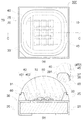
- FIG. 1A is a schematic top view of a light emitting device according to an embodiment of the present invention
- FIG. FIG. 3 is a schematic cross-sectional view (a) to (e) showing an example of a method for manufacturing a light-emitting device according to an embodiment of the present invention.
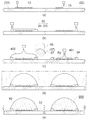
- FIG. 4 is a schematic cross-sectional view (a) to (f) for explaining the relationship between a solid surface and the surface shape of a liquid droplet dropped thereon.
- 1A is a schematic top view of a light emitting device according to an embodiment of the present invention
- FIG. 1A is a schematic top view of a light emitting device according to an embodiment of the present invention
- FIG. 1A is a schematic top view of a light emitting device according to an embodiment of the present invention
- FIG. 1A is a schematic top view of a light emitting device according to an embodiment of the present invention
- FIGS. 2B and 2C are schematic cross-sectional views of a DD section and an EE section.
- 1A is a schematic top view of a light emitting device according to an embodiment of the present invention
- FIG. 1A is a schematic top view of a light emitting device according to an embodiment of the present invention
- FIG. FIG. 3 is a schematic cross-sectional view (a) to (e) showing an example of a method for manufacturing a light-emitting device according to an embodiment of the present invention
- 1A is a schematic top view of a light emitting device according to an embodiment of the present invention
- FIG. 1A is a schematic top view of a light emitting device according to an embodiment of the present invention
- FIG. 1A to 1D are schematic views showing an example of a method for manufacturing a light emitting device according to an embodiment of the present invention. It is the schematic sectional drawing (a) of the light-emitting device which concerns on one Example of this invention, and the schematic sectional drawing (b) of the light-emitting device which concerns on one comparative example.
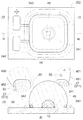
- FIG. 1A is a schematic top view of the light-emitting device according to Embodiment 1
- FIG. 1B is a schematic cross-sectional view showing a cross section AA in FIG. 1A.
- the light emitting device 100 of the example shown in FIG. 1 seals the light emitting element 10, the base member 30 having the conductive member 20 to which the light emitting element 10 is connected and the molded body 25 integrally formed with the conductive member 20, and the light emitting element 10. Sealing member 40 to be provided.
- the base 30 is a package having a pair of positive and negative lead frame conductive members 20 and a resin molded body 25 that integrally holds the conductive members.
- the base body 30 includes a recess 31 on the upper surface side. A part of the bottom surface of the recess 31 is constituted by a part of the surface of the conductive member 20.
- the light emitting element 10 is an LED chip, and is bonded to the bottom surface of the recess 31 of the base with an adhesive (not shown) and connected to the conductive member 20 with a wire.
- the sealing member 40 is a sealing resin provided so as to cover the light emitting element 10 inside the recess 31 of the base.
- the sealing member 40 may contain a phosphor or a diffusing agent.
- the surface of the sealing member 40 protrudes upwards from the base
- the surface on which the surface 45 of the sealing member rises in other words, the surface on which the edge of the sealing member 40 is provided is referred to as “sealing standing surface 37”.
- the sealing upstanding surface 37 is an outward surface 38 facing outward from the top surface of the base body 30.
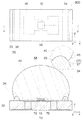
- FIGS. 2A to 2E are schematic cross-sectional views showing an example of a method for manufacturing the light emitting device according to the first embodiment.
- the light emitting device 100 shown in FIG. 1 is manufactured through the following steps. Note that the method for manufacturing a light emitting device of the present invention only needs to include at least a step of forming a sealing member on a substrate on which the light emitting element is mounted, and the manufacturing method described here is merely an example.
- a molded body 25 is integrally formed with the conductive member 20 to form a base body 30.
- a plate-like member in which a plurality of conductive members 20 are connected is sandwiched between an upper die and a lower die that have been processed into a predetermined shape, and a fluid state (liquid, sol).
- a fluid state liquid, sol
- the constituent material of the molded body 25 in the form of a slurry or a slurry is injected and solidified. Thereafter, when the molded body 25 is released from the mold, a plurality of base bodies 30 in a state of being connected to each other are obtained.
- the light emitting element 10 is mounted on the substrate 30. Specifically, the light emitting element 10 is bonded to the base 30 with an adhesive, and is further connected to the conductive member 20 with a wire.
- the sealing member 40 is formed on the base body 30.
- the sealing member is formed by dropping (potting).
- the dropping method is an inexpensive molding method that does not use a molding machine or a mold as compared with a compression molding method, a transfer molding method, an injection molding method, or a casting molding method.
- the sealing member 40 in a fluid state liquid, sol, or slurry
- the stop member 40 is solidified by heating or cooling.
- the sealing member 40 is molded so that at least a part of the sealing standing surface 37 is the outward surface 38.
- the sealing member 40 is shaped such that at least a part of the surface 45 rises from the outward surface 38 of the base body 30.
- the angle formed between the tangent line of the surface 45 of the sealing member 40 (at the contact point between the outward surface 38 and the edge of the sealing member 40) and the outward surface 38 is a substantially contact angle.
- the “contact angle” is determined by the physical properties of the sealing member 40 and the outward surface 38 in a state having fluidity before solidification.
- the sealing member 40 may be solidified with the base body 30 turned upside down, that is, with the upper surface of the base body 30 onto which the sealing member 40 is dropped facing downward in the vertical direction. If it does so, the sealing resin 40 can be solidified in the state which the sealing resin 40 in the state which has fluidity
- the plate-shaped member is cut to separate the light emitting device 100 into individual pieces.
- the base member 30 may be separated into pieces by cutting the plate member.
- the surface of the sealing resin rises from the upper surface that is higher (that is, inward) from the front of the horizontal direction of the damming portion or from the front of the resin flow direction. Yes.
- the surface of the convex lens rises from the inner surface of the annular light reflecting member.
- the sealing member since the sealing member is provided on the base as described above, the surface of the sealing member can be relatively stably formed into a convex surface that protrudes highly, and the light extraction efficiency is sufficient. Can be increased.
- the inventors have raised the surface of the sealing member from the outward surface of the substrate, contrary to the conventional idea.
- the present inventors have found that it is a secret that can be molded relatively stably. The principle will be described below.
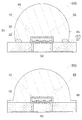
- 3 (a) to 3 (f) are schematic cross-sectional views for explaining the relationship between the solid surface and the surface shape of the liquid droplets dropped on the solid surface.
- the droplet L dropped on the flat surface of the solid S has a convex curved surface that forms a contact angle ⁇ [degree] with the surface of the solid S due to its surface tension.
- the contact angle ⁇ is defined as an angle formed by the tangent to the surface of the droplet L and the surface of the solid S (an angle including the droplet L) at the contact point between the surface (edge) of the droplet L and the solid S.
- This contact angle ⁇ is determined by the surface tension of the material constituting each of the droplet L and the solid S.
- the contact angle ⁇ takes a specific value.
- the surface tension of the droplet L is ⁇ L
- the surface tension of the solid S is ⁇ S
- the interfacial tension ⁇ SL between the droplet L and the solid S is as follows (Young's equation)
- the surface of the solid S is inclined at an angle ⁇ [degree] from the horizontal plane as shown in FIG.
- the contact angle of the droplet L with respect to the surface of the inclined solid S is maintained substantially ⁇ , but the pseudo contact angle with respect to the horizontal plane is approximately ⁇ + ⁇ . Therefore, as shown in FIG. 3C, the height h of the droplet L can be increased by raising the surface of the droplet L from the outward surface facing outward in the top view of the solid S. As shown in FIG.
- tangential plane when the surface of the solid S is a convex curved surface, a plane (“tangential plane”) that contacts the surface of the solid S at the contact point between the solid S and the edge of the droplet L. Call).
- the tangential plane is inclined by an angle ⁇ [degree] with respect to the horizontal plane, and the pseudo contact angle of the droplet L with respect to the horizontal plane is substantially ⁇ + ⁇ .
- the contact angle between the droplet L and the horizontal upper surface of the solid S is the original contact angle.
- a phenomenon called “wetting pinning effect” that cannot get over the edge part until reaching the sum of ⁇ and the downward angle of the outward surface of the edge part (inclination angle from the upper surface) ⁇ [degrees]. is there.
- the contact angle of the droplet L can take any value from ⁇ to ⁇ + ⁇ . Therefore, the height of the droplet L can be increased by utilizing this “wetting pinning effect”.
- the droplet L at this time is in a relatively unstable state, and even if an attempt is made to control the height of the droplet L using this phenomenon, the height varies greatly. Further, as described above, in order to control the height of the droplet L using this phenomenon, high working accuracy is required at the edge portion.
- FIG. 3C when the surface of the droplet L rises from the outward surface of the solid S, the droplet L has a substantially original contact angle ⁇ with respect to the outward surface of the solid S. Therefore, the height can be obtained with good reproducibility. As shown in FIG.
- the contact angle ⁇ of the sealing member 40 is the sealing It is determined by the surface tension of the member 40, the surface tension of the base body 30 on which the edge of the sealing member 40 is provided, and the interfacial tension between the sealing member 40 and the base body 30.
- the edge of the sealing member 40 on the outward surface 38, the angle formed by the tangent to the surface 45 of the sealing member (at the contact point between the outward surface 38 and the edge of the sealing member) and the outward surface 38.
- the sealing member 40 is formed so that at least a part of the sealing rising surface 37 is the outward surface 38, and thus the surface 45 of the sealing member is easily raised in the vertical direction from the outward surface 38. Become.
- the surface of the sealing member 40 can be easily formed into a highly protruding convex surface, preferably a convex curved surface, and thus a substantially spherical surface.
- the surface shape can be obtained with good reproducibility. Therefore, a light emitting device having excellent light extraction efficiency can be manufactured at low cost.
- the sealing member surface into a highly protruding convex surface by forming the sealing member by dropping after forming a film having a small surface tension over the entire upper surface of the substrate.
- the adhesion between the base and the sealing member may be significantly reduced due to the coating interposed between the base and the sealing member.
- the sealing member is basically in direct contact with the surface of the base, and high adhesion between the base and the sealing member is obtained. Can be provided. In particular, by raising the surface of the sealing member from the outward surface of the base, the edge of the sealing member acts so as to be locked to the base, and the adhesion between the base and the sealing member can be further enhanced. .
- the base body 30 includes a protrusion 33.
- the base body 30 of this example includes a groove 35 in addition to the protrusion 33. It may be said that the protrusion 33 is formed by the groove 35. Since the base body 30 includes the protrusions 33 or the grooves 35, the outward surface 38 is provided on the inner side of the outermost end surface of the base body 30. Then, at least a part of the surface 45 of the sealing member can be raised from the outward surface 38 of the protrusion 33 or the groove 35.
- the outflow of the sealing member 40 to the outside of the base body 30 is suppressed, and the surface 45 of the sealing member can be stably formed into a highly protruding convex surface inside the outermost end face of the base body 30. it can. Moreover, it can suppress that the exposed part of the electrically-conductive member 20 used as the terminal part for external connection is contaminated with the oozing-out component of the sealing member 40.
- the base body includes a protrusion or a groove, and at least a part of the sealing standing surface is provided on the outward surface of the protrusion or the groove.
- substrate is provided with both a languages
- channel may be provided mutually spaced apart.
- the protrusions and grooves of the base body can be omitted, and at least a part or the whole of the sealing upright surface may be provided on the outward surface which is the outermost end surface of the base body.
- the outward surface 38 of the protrusion 33 or the groove 35 is a lower surface continuous with the convex curved surface.
- the sealing member in a fluid state is dropped onto the base and reaches the edge formed by the outward surface of the base and the continuous surface above the base.
- the outward surface is a flat surface bent from the upper surface, the sealing member is temporarily accumulated on the upper surface of the outward surface due to the “wetting pinning effect” described above.
- a sealing member gets over the edge part there exists a possibility of flowing out vigorously by the weight of itself enlarged and destroying the surface shape.
- the outward surface of the substrate has a convex curved surface at the uppermost position, as described above, the “wetting pinning effect” can be suppressed and the sealing member can be smoothly moved onto the outward surface. . Thereby, it can make it easy to shape
- at least a part of the sealing upright surface 37 may be a convex curved surface on the outward surface 38, or may be a surface that continues beyond the convex curved surface.
- the outward surface 38 is preferably a convex curved surface or a lower surface continuous with the convex curved surface.
- the uppermost surface of the outward surface 38 is a convex curved surface, so that chipping of the molded body 25 due to biting on the mold is suppressed and the moldability of the molded body 25 is improved. Can be increased.
- the surface of the sealing member 40 can be protruded higher as the inclination angle ( ⁇ ) of the outward surface 38 from the substantially horizontal upper surface of the base body 30 is larger.
- the inclination angle ( ⁇ ) of the outward surface 38 is preferably 90 degrees or less in consideration of the releasability of the base body 30 from the mold. Therefore, the inclination angle ( ⁇ ) of the outward surface 38 that becomes the sealing rising surface 37 is preferably 45 to 90 degrees, and more preferably 70 to 90 degrees.
- the inward surface 391 of the protrusion 33 facing the inner side in the top view of the base body has a convex curved surface at the uppermost position.
- a sealing member in a fluid state is dropped on a base and reaches an edge formed by an inward surface of the base and a continuous surface on the upper side.
- the inward surface is a flat surface bent from the upper surface, the sealing member is temporarily accumulated on the inward surface due to the “wetting pinning effect” described above.
- a sealing member gets over the edge part there exists a possibility of flowing out vigorously by the weight of itself enlarged, and also flowing out beyond an outward surface.
- the inward surface 391 of the base body 30 has a convex curved surface at the uppermost position, as described above, the “wetting pinning effect” is suppressed, and the sealing member 40 is continuous to the upper side, and thus outward. It can be moved smoothly onto the surface 38. Thereby, it can make it easy to shape
- at least a part, most preferably all, of the inwardly facing surface 391 inside the sealing rising surface 37 and facing the top surface of the base body is located at the topmost position. It preferably has a convex curved surface.
- the protrusion 33 and the groove 35 are provided in a perfect circle shape surrounding the light emitting element 10 in a top view of the base body 30.
- the protrusion 33 or the groove 35 provides an outward surface 38 for raising the surface 45 of the sealing member, and functions as a barrier for blocking the sealing member 40 in a fluid state.
- the protrusion or the groove is provided in a frame shape surrounding the light emitting element.
- the surface 45 of the sealing member is easily formed from the protrusion to the protrusion or from the groove to the groove, the symmetry of the surface shape of the sealing member 40 can be enhanced.
- the protrusion 33 or the groove 35 is preferably provided in an annular shape in the top view of the base body 30, and is preferably provided in an elliptical shape, and more preferably provided in a perfect circular shape.
- the surface of the sealing member 40 can be shape
- the protrusion 33 or the groove 35 is disposed so that the light emitting element 10 is substantially at the center, thereby improving the symmetry of light distribution.
- the protrusion is more preferable than the groove from the viewpoint of a barrier for blocking the sealing member having fluidity.
- the base body 30 includes a recess 31, and the protrusion 33 and the groove 35 are provided in the recess 31.
- the sealing member 40 is provided inside the recess 31.
- the base body includes a recess in which the light emitting element is placed inside, and the sealing upright surface is provided in the recess. Since the base body 30 includes the concave portion 31, the outflow of the sealing member 40 to the outside of the base body 30 can be suppressed, and the sealing member 40 can be easily molded stably in the concave portion 31. Further, since the sealing member 40 is provided inside the recess 31, the apparatus can be reduced in size.
- the molded body 25 constituting the recess 31 functions as a barrier that protects the sealing member 40 from damage due to external force and contamination by dust.
- the inner wall surface of the recess 31 functions as a reflecting mirror that reflects light emitted from the light emitting element 10 toward the front of the device (above the base 30) and effectively extracts the light, thereby increasing the front luminous intensity of the light emitting device.
- these effects can be remarkably obtained.
- the sealing rising surface 37 is provided on the outward surface 38 of the groove 35, and the groove 35 has an inward surface 392 that faces the outward surface 38. is doing.
- the inward surface 392 is a part of the inner wall surface of the recess 31.
- the base body has an inward surface facing the inner side in the top view of the base body on the outer side than the outward surface on which the sealing upstanding surface is provided.
- the light emitted from the edge of the sealing member 40 provided on the outward surface 38 of the base body 30 is directed to the front of the apparatus by the inward surface 392 and / or the bottom surface between the inward surface and the outward surface 38. It can be reflected and taken out effectively.
- the inward surface 392 that faces the outward surface 38 on which the sealing standing surface 37 is provided is inclined so as to open upward or curved in such a manner. Thereby, the light radiate
- the inward surface 392 that faces the outward surface 38 on which the sealing standing surface 37 is provided is preferably provided to substantially the same height as the outward surface 38, and is provided to extend higher than the outward surface 38. More preferably. Thereby, it is easy to reflect the light emitted from the edge of the sealing member 40 provided on the outward surface 38 of the base body 30 to the front of the apparatus.
- Such an inward surface 392 is difficult to be provided in a molding method of a sealing member using a molding machine or a mold because the molding machine or the mold interferes.
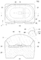
- FIG. 4A is a schematic top view of the light-emitting device according to Embodiment 2
- FIG. 4B is a schematic cross-sectional view showing a BB cross section in FIG. 4A.
- the light emitting device 200 of the example shown in FIG. 4 seals the light emitting element 10, the base member 30 having the conductive member 20 to which the light emitting element 10 is connected and the molded body 25 integrally formed with the conductive member 20, and the light emitting element 10. Sealing member 40 to be provided.
- the base 30 is a package having a pair of positive and negative lead frame conductive members 20 and a resin molded body 25 that integrally holds the conductive members.
- the base body 30 includes a recess 31 on the upper surface side. A part of the bottom surface of the recess 31 is constituted by a part of the surface of the conductive member 20.
- the light emitting element 10 is an LED chip, and is bonded to the bottom surface of the recess 31 of the base with an adhesive (not shown) and connected to the conductive member 20 with a wire.
- the sealing member 40 is a sealing resin provided so as to cover the light emitting element 10 inside the recess 31 of the base.
- the base body 30 includes a first protrusion 331 and a second protrusion 332 provided outside the first protrusion 331.
- the base body 30 of the present example includes a first groove 351 and a second groove 352 provided outside the first groove 351 in addition to these protrusions. It can be said that the first and second protrusions are formed by the first and second grooves, respectively.
- the base body includes the first protrusion or the first groove and the second protrusion or the second groove outside the first protrusion or the first groove. It is preferable to be provided on the outward face of any one of the second protrusion and the first and second grooves.
- the base body 30 includes the plurality of protrusions 331 and 332 or the plurality of grooves 351 and 352, the plurality of outward faces 38 are provided on the inner side of the outermost end surface of the base body 30. Then, at least a part of the surface 45 of the sealing member can be raised from the outward surface 38 of any one of the protrusions 331 and 332 or the grooves 351 and 352.
- the outward surface 38 as the sealing standing surface can be selected, and the sealing member 40 is adjusted while adjusting the size of the sealing member 40.
- the surface of 40 can be formed into a convex surface projecting high.
- channel 351 is provided inside the wire connection part to which the wire of the electrically-conductive member 20 is connected. Thereby, it can suppress that the wire connection part of the electrically-conductive member 20 is contaminated with the oozing-out component of the adhesive which adhere
- the first protrusion 331 or the first groove 351 can be formed in the conductive member 20 by press working, die molding, or the like.
- the sealing member 40 includes a first sealing portion 401 that seals the light emitting element 10, and a second sealing portion 402 that seals the first sealing portion 401. It is equipped with.
- the first sealing portion 401 includes at least a part of the first sealing rising surface 371 on which the surface 451 of the first sealing portion rises among the constituent surfaces of the base body 30 as the first protrusion 331 or the first The outer surface 38 of the groove 351 is formed.
- the second sealing portion 402 has at least a part of the second sealing rising surface 372 on which the surface 452 of the second sealing portion rises among the constituent surfaces of the base body 30 as the second protrusion 332 or the second projection.
- each sealing portion (each layer) can be relatively stably molded into a convex surface that protrudes highly. It is easy to suppress the reflection of light at the interface of the sealing portion and increase the light extraction efficiency.
- each sealing portion may be made of the same material and have the same refractive index, but from the light emitting element 10 by gradually making the refractive index of each sealing portion closer to the refractive index of air. Light can be efficiently extracted into the sealing member 40, and reflection of light at the interface between the two sealing portions can be suppressed to further increase the light extraction efficiency.
- the refractive index of the second sealing portion 402 is preferably lower than the refractive index of the first sealing portion 401.
- the second sealing portion 402 may be molded after the first sealing portion 401 is completely solidified, but by molding the first sealing portion 401 in a semi-solidified or unsolidified state, The adhesion between the first sealing portion 401 and the second sealing portion 402 can be improved.
- the 1st sealing part 401 is an internal area
- the surface 451 of the first sealing portion 401 rises from the end of the upper surface serving as a boundary with the first protrusion 331 of the base body 30 or the outward surface 38 of the first groove 351.
- a preferable aspect similar to that of the inward surface 392 described above can be applied to the first sealing portion 401 also on the inward surface facing the outward surface 38 of the first groove 351.
- the sealing member 40 includes the phosphor 50 that is excited by the light emitted from the light emitting element 10 only in the first sealing portion 401.
- the wavelength conversion and scattering of light by the phosphor 50 is performed only in the first sealing portion 401, that is, in the vicinity of the light emitting element 10 in the sealing member 40.
- the light source can be made smaller with respect to the surface of the sealing member, and the light extraction efficiency can be increased.
- the surface of the first sealing portion 401 can be formed into a highly protruding convex surface, the variation in the optical path length in each direction in the first sealing portion 401 can be reduced, and the first sealing portion 401 Even if the phosphor 50 is dispersed in 401, it is possible to emit light with substantially uniform chromaticity.
- the fluorescent substance 50 may be settled and a diffusing agent may be disperse
- the uppermost position of the outward surface 38 of the first protrusion 331 or the first groove 351 is a flat surface.
- the outward surface 38 is most preferably a convex curved surface, but the downward angle from the upper plane continuous with the outward surface ( The plane may be preferably 45 ° or less, more preferably 30 ° or less.
- the plane may be preferably 45 ° or less, more preferably 30 ° or less.
- the “upper plane continuous with the outward surface” is not limited to the substantially horizontal upper surface of the base body 30 and may be an outward surface. That is, the outward surface 38 may be configured by a plurality of planes in which the descending angle of the lower plane from the upper plane is preferably 45 degrees or less, more preferably 30 degrees or less.
- FIG. 5A is a schematic top view of the light-emitting device according to Embodiment 3, and FIG. 5B is a schematic cross-sectional view showing a CC cross section in FIG. 5A.
- the light emitting device 300 of the example shown in FIG. 5 seals the light emitting element 10, the base member 30 having the conductive member 20 to which the light emitting element 10 is connected and the molded body 25 integrally formed with the conductive member 20, and the light emitting element 10. Sealing member 40 to be provided.
- the base 30 is a package having a pair of positive and negative lead frame conductive members 20 and a resin molded body 25 that integrally holds the conductive members.
- the base body 30 includes a recess 31 on the upper surface side. A part of the bottom surface of the recess 31 is constituted by a part of the surface of the conductive member 20.
- the light emitting element 10 is an LED chip, and a plurality of light emitting elements 10 are bonded to the bottom surface of the concave portion 31 of the base with an adhesive (not shown) and connected to the conductive member 20 with a wire.
- the sealing member 40 is a sealing resin provided on the base 30 so as to cover the light emitting element 10.
- the base body 30 includes a protrusion 33 formed on the outside of the recess 31.
- the protrusion 33 or the groove on the outer side of the recess 31 it becomes easier to form a larger sealing member 40 having at least a part of the sealing rising surface 37 as the outward surface 38 of the protrusion or groove, It is easy to increase the light extraction efficiency.
- the concave portion 31 can be easily configured to have a large opening area so that substantially the entire area of the inner wall surface can be used as a reflecting mirror, and the light extraction efficiency can be easily increased. Therefore, it is easy to increase the light extraction efficiency even when the light source is relatively large or the substrate is relatively small.
- the sealing member 40 is formed in two stages, and the phosphor 50 excited by the light emitted from the light emitting element 10 is limited to the first sealing portion 401 in the lower layer.
- the first sealing portion 401 covers all the light emitting elements 10 and is filled up to the upper surface of the recess 31. Thereby, the inside of the 1st sealing part 401 is made into a surface light source.
- the first sealing portion 401 may contain a diffusing agent.
- the upper second sealing portion 402 is formed so that at least a part of the sealing rising surface 37 is the outward surface 38 of the protrusion 33, and has a highly convex surface 45 (452). . Thereby, a light-emitting device with a high luminous flux can be obtained.
- the protrusion 33 is provided in a rectangular frame shape with rounded corners along the outline of the recess 31 in the top view of the base body 30. It is preferable that at least the corners of the protrusions or the grooves are curved as described above in the top view of the base body or the entire shape as in the perfect circle shape described in the first and second embodiments.
- the protrusion or the groove is bent and bent in a top view of the substrate, the surface of the sealing member rising from the vicinity of the corner is distorted.
- the protrusion or the groove does not necessarily have to be provided along the outline of the concave portion.
- an annular protrusion or groove may be provided for the rectangular concave portion.
- the coating 60 having a critical surface tension of 50 mN / m or less is limited to the outward surface 38 on which the sealing rising surface 37 of the base body 30 is provided and the constituent surface outside the outward surface 38. Is formed.
- the contact angle of the sealing member 40 contact angle ⁇ of the droplet L in FIG. 3 is the substrate (FIG. 2). Then, it becomes so large that the surface tension of the outward surface 37 (solid S of FIG. 3) of the molded object 25) is small.
- the sealing member 40 Before dropping the sealing member onto the substrate, only the outward surface on which the sealing upright surface of the substrate is provided, or the outward surface on which the sealing upstanding surface of the substrate is provided and the configuration outside the outward surface By forming a film having a small surface tension only on the surface, the surface of the sealing member can easily rise from the outward surface. Thereby, the surface of the sealing member 40 can be easily formed into a convex surface that protrudes high, and the light extraction efficiency can be easily increased. Further, by limiting the range in which the coating film 60 is provided in this way, the sealing member 40 is in direct contact with the surface of the base body 30 on the inner side of the outwardly facing surface 38, and thus the high adhesion between the base body 30 and the sealing member 40.
- the molded body 25 is preferably made of a material having a critical surface tension of more than 50 mN / m because cohesive force for securing solder heat resistance and adhesion between the sealing member 40 are necessary.
- the coating 60 is preferably made of a material having a critical surface tension of 50 mN / m or less. Specific materials for the coating 60 include a fluororesin material and a silicone material. Among these, silicone oil is preferable because it is absorbed by the sealing member during the solidification of the sealing member and hardly deteriorates the adhesion with the substrate.
- FIG. 6 (a) is a schematic top view of the light emitting device according to Embodiment 4, and FIGS. 6 (b) and 6 (c) show a DD section and an EE section in FIG. 6 (a), respectively. It is a schematic sectional drawing shown.
- the light emitting device 400 of the example shown in FIG. 6 seals the light emitting element 10, the base member 30 having the conductive member 20 to which the light emitting element 10 is connected and the molded body 25 integrally formed with the conductive member 20, and the light emitting element 10. Sealing member 40 to be provided.
- the base 30 is a package having a pair of positive and negative lead frame conductive members 20 and a resin molded body 25 that integrally holds the conductive members.
- the base body 30 includes a recess 31 on the upper surface side. A part of the bottom surface of the recess 31 is constituted by a part of the surface of the conductive member 20. A terminal portion for external connection of the conductive member 20 is provided to extend on the end face of the molded body 25.
- the light emitting element 10 is an LED chip, and is bonded to the bottom surface of the recess 31 of the base with an adhesive (not shown) and connected to the conductive member 20 with a wire.
- the sealing member 40 is a sealing resin provided on the base 30 so as to cover the light emitting element 10.
- the lower surface (back surface) of the substrate 30 is the mounting surface.
- the light emitting device 400 of the example shown in FIG. 6 has an end surface (side surface) of the base 30 as a mounting surface, and a vertical direction (y direction in the figure) substantially perpendicular to the end surface serving as the mounting surface is mounted. It becomes the thickness (height) direction.
- Such a light emitting device 400 is installed on the side of the light guide plate as a light source for a backlight of a liquid crystal display, for example. Therefore, the base body 30 has a vertically long and horizontally long shape in a top view in order to reduce the thickness, and accordingly, the recess 31 has a similar shape.
- the sealing member 40 is shaped so that at least a part of the sealing standing surface 37 is an outward surface 38 of the protrusion 33. As a result, at least in the lateral direction, the surface of the sealing member 40 can be formed into a highly projecting convex surface, and the light extraction efficiency can be increased.
- the protrusions or grooves are not limited to the frame shape, and may be provided in a band shape. Thereby, it is easy to form a protrusion or a groove in a small size, and it is easy to provide an outward surface in a small area inside the outermost end surface of the base. In that case, it is preferable that at least two protrusions or grooves are provided so as to sandwich the light emitting element. Then, since the surface of the sealing member is easily formed from the protrusion to the protrusion or from the groove to the groove, the symmetry of the surface shape of the sealing member can be enhanced. In addition, a plurality of protrusions or grooves may be provided apart from each other as shown by a broken line, and may be further scattered.
- FIG. 7A is a schematic top view of the light-emitting device according to Embodiment 5, and FIG. 7B is a schematic cross-sectional view showing the FF cross section in FIG. 7A.
- the light emitting device 500 of the example shown in FIG. 7 has substantially the same configuration as the light emitting device of the above-described fourth embodiment except for the shapes of the recess 31 and the protrusion 33.
- the shape of the recess 31 in a top view is rectangular, which is excellent in that the opening area of the recess 31 can be easily widened.
- the top view shape of the recess 31 is a shape (oval shape) in which semicircles are combined on both sides (left and right) of the rectangle.
- the protrusion 33 is formed in the strip
- the corners or the whole of the base body 30 is curved in a top view.
- FIG. 8A is a schematic top view of the light-emitting device according to Embodiment 6, and FIG. 8B is a schematic cross-sectional view showing a GG section in FIG. 8A.
- the light emitting device 600 of the example shown in FIG. 8 encloses the light emitting element 10, the wiring board 22 on which the light emitting element 10 is placed, and the base 30 having the protrusions 34 provided on the upper surface of the wiring board 22, and the light emitting element 10. Sealing member 40 to be stopped.
- the base body 30 includes a wiring board 22 having wiring electrodes on the upper surface, and a protrusion 34 that is a white resin molded body provided in a frame shape on the upper surface.
- the light emitting element 10 is an LED chip, and a plurality of light emitting elements 10 are bonded to the inside of the protrusion 34 on the upper surface of the wiring substrate 22 with an adhesive (not shown), and are connected to the wiring electrodes with wires.
- the sealing member 40 is a sealing resin provided on the base 30 so as to cover the light emitting element 10. In particular, in this example, the sealing member 40 is divided into two parts, and the phosphor 50 is excited only by the light emitted from the light emitting element 10 only in the first sealing part 401 in the lower layer. Contains.
- the first sealing portion 401 covers all the light emitting elements 10 and is filled up to substantially the top of the protrusion 34. Thereby, the inside of the 1st sealing part 401 is made into a surface light source. Note that the first sealing portion 401 may contain a diffusing agent.
- the surface of the sealing member 40, and the surface of the 2nd sealing part 402 of the upper layer more specifically, protrudes upwards from the base
- at least a part, and most preferably all, of the seal rising surface 37 is an outward surface 27 facing outward in the top view of the protrusion 34.
- FIGS. 9A to 9E are schematic cross-sectional views showing an example of a method for manufacturing the light emitting device according to Embodiment 6.
- FIGS. The light emitting device 600 shown in FIG. 8 is manufactured through the following processes.
- the first step of forming a base by providing a protrusion on the upper surface of the wiring substrate on which the light emitting element is mounted, and the sealing member for sealing the light emitting element are formed.
- the manufacturing method described here is merely an example as long as it includes at least the second step.
- the light emitting element 10 is mounted on the wiring board 22. Specifically, the light emitting element 10 is bonded to the wiring board 22 with an adhesive, and further connected to the wiring electrodes of the wiring board 22 with wires.
- the wiring substrate 22 a composite substrate capable of forming a plurality of light emitting devices is used.
- the base 30 is formed by providing protrusions 34 on the upper surface of the wiring board 22.
- a constituent material of the protrusion 34 in a fluid state (liquid, sol, or slurry) is dropped on the upper surface of the wiring substrate 22 and drawn in a frame shape so as to surround the light emitting element 10. It is solidified by heating or cooling. Note that the order of the light emitting element mounting step and the protrusion forming step may be reversed.
- the sealing member 40 is formed on the base body 30.
- the sealing member is formed by dropping (potting).
- the dropping method is an inexpensive molding method that does not use a molding machine or a mold as compared with a compression molding method, a transfer molding method, an injection molding method, or a casting molding method. Further, in the dropping method, the flow of the constituent material of the sealing member at the time of forming the sealing member is small, and deformation of the wire can also be suppressed.
- the sealing member 40 in a fluid state liquid, sol, or slurry
- a fluid state liquid, sol, or slurry
- the stop member 40 is solidified by heating or cooling. At this time, the sealing member 40 is formed so that at least a part of the sealing standing surface 37 is the outward surface 27 of the protrusion 34. In other words, the sealing member 40 is formed such that at least a part of the surface 45 rises from the outward surface 27 of the protrusion 34. As described above, the angle formed between the tangent to the surface 45 of the sealing member 40 (at the contact point between the outward surface 27 and the edge of the sealing member 40) and the outward surface 27 is a substantially contact angle.
- the constituent material of the first sealing portion 401 containing the phosphor 50 is dropped on the inside of the protrusion 34, and then the constituent material of the second sealing portion 402 is dropped thereon.
- the second sealing portion 402 may be formed after the first sealing portion 401 is completely solidified, but the first sealing portion 401 is formed in a semi-solidified state or an unsolidified state, The adhesion between the sealing portion 401 and the second sealing portion 402 can be improved.
- the sealing member 40 may be solidified with the base body 30 turned upside down, that is, with the upper surface of the base body 30 onto which the sealing member 40 is dropped facing downward in the vertical direction. If it does so, the sealing resin 40 can be solidified in the state which the sealing resin 40 in the state which has fluidity
- the wiring board 22 (composite board) is cut to separate the light emitting device 600 into pieces.
- the base body 30 may be separated into pieces, or the wiring substrate 22 separated into pieces for a single light emitting device from the beginning may be used.
- the sealing member is provided on the base as described above, the surface of the sealing member can be relatively stably formed on the projecting surface, and the light extraction efficiency can be sufficiently increased. .
- the contact angle ⁇ of the sealing member 402 is determined by the surface tension of the sealing member 402, It is determined by the surface tension of the base body 30 (specifically, the protrusion 34) on which the edge of the sealing member 402 is provided and the interfacial tension between the sealing member 402 and the base body 30 (protrusion 34).
- the sealing member 402 is provided on the outward surface 27 of the protrusion 34, the tangent to the surface 45 of the sealing member (at the contact point between the outward surface 27 and the edge of the sealing member), the outward surface 27, and Is approximately the contact angle ⁇ , but the angle formed between the tangent to the surface 45 of the sealing member and the horizontal plane can be greater than the contact angle ⁇ . That is, the sealing member 40 is formed such that at least a part of the sealing rising surface 37 is the outward surface 27 of the projection 34, so that the surface 45 of the sealing member starts in the vertical direction from the outward surface 27. Easier to get up.
- the surface of the sealing member 40 can be easily formed into a highly protruding convex surface, preferably a convex curved surface, and thus a substantially spherical surface. Moreover, the surface shape can be obtained with good reproducibility. Therefore, a light emitting device having excellent light extraction efficiency can be manufactured at low cost.
- the sealing member is also possible to form the sealing member with a highly projecting convex surface by forming the sealing member by dropping after forming a film having a small surface tension over the entire upper surface of the substrate.
- the adhesion between the base and the sealing member may be significantly reduced due to the coating interposed between the base and the sealing member.
- the sealing member is basically in direct contact with the surface of the base, and high adhesion between the base and the sealing member is obtained. Can be provided.
- the edge of the sealing member acts so as to be locked to the protrusion, and the adhesion between the base and the sealing member can be further enhanced. .
- the outward surface 27 of the protrusion 34 is a convex curved surface.
- the sealing member having fluidity is dropped onto the base and reaches the edge formed by the outward surface of the protrusion and the surface continuous above the protrusion.
- the sealing member is temporarily accumulated on the upper surface of the outer surface due to the above-described “wetting pinning effect”. .
- a sealing member gets over the edge part, there exists a possibility of flowing out vigorously by the weight of itself enlarged and destroying the surface shape.
- the outward surface of the protrusion has a convex curved surface at the top, as described above, the “wetting pinning effect” can be suppressed and the sealing member can be smoothly moved onto the outward surface. .
- the surface of the sealing member 40 can be easily and stably formed on a convex surface that protrudes highly.
- at least a part of the sealing standing surface 37 may be a convex curved surface on the outward surface 27, or may be a surface that extends beyond the convex curved surface and continues to the lower side thereof.
- the outward surface 27 is preferably a convex curved surface or a lower surface continuous with the convex curved surface.
- the uppermost surface of the outward surface 27 of the protrusion 34 is formed as a convex curved surface, thereby suppressing the chipping of the protrusion 34 due to biting into the mold and the moldability of the protrusion 34. Can be increased.
- the inward surface 29 facing the inner side in the top view of the protrusion 34 is a convex curved surface.
- the sealing member in a fluid state is dropped on the base and reaches an edge portion formed by an inward surface of the protrusion and a surface continuous thereabove.
- the inward surface of the protrusion is a flat surface bent from the upper surface, the sealing member is temporarily accumulated on the inward surface due to the “wetting pinning effect” described above.
- a sealing member gets over the edge part there exists a possibility of flowing out vigorously by the weight of itself enlarged, and also flowing out beyond an outward surface.
- the inward surface 29 of the protrusion 34 has a convex curved surface at the uppermost position, as described above, the “wetting pinning effect” is suppressed, and the surface of the sealing member 40 that is continuous to the upper side thereof is extended outward. It can be moved smoothly onto the surface 27. As a result, the surface of the sealing member 40 can be easily and stably formed on a convex surface that protrudes highly.
- at least a part, most preferably all, of the inwardly facing surface 29 of the constituent surface of the base body 30 located on the inner side of the sealing standing surface 37 and facing the inner side of the projection as viewed from above is projected to the uppermost position. It is preferable to have a curved surface.
- the protrusion 34 is provided in an annular shape surrounding the light emitting element 10 when viewed from above.
- the protrusion 34 provides an outward surface 27 for raising the surface 45 of the sealing member, and functions as a barrier for blocking the sealing member 40 in a fluid state.
- the protrusion is provided in a frame shape surrounding the light emitting element.
- the protrusion 34 is preferably provided in an annular shape in a top view, and in particular, is preferably provided in an elliptical shape, and more preferably provided in a perfect circular shape.
- the surface of the sealing member 40 can be formed in a convex surface with little distortion, light extraction efficiency can be easily improved, and light distribution excellent in symmetry can be obtained.
- the protrusions 34 are arranged so that the light emitting element 10 is substantially at the center, thereby improving the symmetry of light distribution.
- FIG. 10A is a schematic top view of the light-emitting device according to Embodiment 7, and FIG. 10B is a schematic cross-sectional view showing the HH cross section in FIG.
- the light emitting device 700 of the example shown in FIG. 10 encloses the light emitting element 10, the substrate 30 on which the light emitting element 10 is placed, the base 30 having the protrusions 34 provided on the upper surface of the wiring board 22, and the light emitting element 10. Sealing member 40 to be stopped.
- the base body 30 includes a wiring substrate 22 having wiring electrodes on the upper surface, a first protrusion 341 provided on the upper surface, and a second protrusion 342 on the outer side.
- the first and second protrusions 341 and 342 are white resin molded bodies formed in a predetermined shape in advance, and are bonded to the upper surface of the wiring board 22 with an adhesive.
- the light emitting element 10 is an LED chip, and one is bonded inside the protrusion 34 on the upper surface of the wiring substrate 22 with an adhesive (not shown), and is connected to the wiring electrode by a wire.
- the sealing member 40 is a sealing resin provided on the base 30 so as to cover the light emitting element 10.
- the first protrusion and the second protrusion outside the first protrusion are provided on the upper surface of the wiring substrate, and in the second step, at least a part of the sealing standing surface is provided.
- the surface 45 of the sealing member can be raised from the outward surface 27 of any one of the protrusions 341 and 342.
- the surface of the member 40 can be formed into a convex surface that protrudes highly.
- the first protrusion 341 is provided outside the wire connection portion to which the wire of the wiring electrode of the wiring substrate 22 is connected, thereby suppressing or avoiding the distortion of the surface shape of the sealing member 40 due to the wire. Can do.
- the first protrusion 341 may be provided on the inner side of the wire connection portion to which the wire of the wiring electrode of the wiring board 22 is connected. Thereby, it can suppress that the wire connection part of the wiring electrode of the wiring board 22 is contaminated with the oozing-out component of the adhesive which adhere
- the sealing member 40 includes a first sealing portion 401 that seals the light emitting element 10, and a second sealing portion 402 that seals the first sealing portion 401. It is equipped with.
- the first sealing portion 401 includes at least a part of the first sealing rising surface 371 where the surface 451 of the first sealing portion rises among the constituent surfaces of the base body 30, and the outward surface 27 of the first protrusion 341. It is formed as follows.
- the second sealing portion 402 has at least a part of the second sealing rising surface 372 on which the surface 452 of the second sealing portion rises among the constituent surfaces of the base body 30, and the outward surface 27 of the second protrusion 342. It is formed as follows.
- each sealing portion can be formed relatively stably on a convex surface that protrudes highly. It is easy to suppress the reflection of light at the interface of the sealing portion and increase the light extraction efficiency.
- each sealing portion may be made of the same material and have the same refractive index, but from the light emitting element 10 by gradually making the refractive index of each sealing portion closer to the refractive index of air. Light can be efficiently extracted into the sealing member 40, and reflection of light at the interface between the two sealing portions can be suppressed to further increase the light extraction efficiency.
- the refractive index of the second sealing portion 402 is preferably lower than the refractive index of the first sealing portion 401.
- the second sealing portion 402 may be formed after the first sealing portion 401 is completely solidified, but by forming the first sealing portion 401 in a semi-solidified or non-solidified state, The adhesion between the first sealing portion 401 and the second sealing portion 402 can be improved. Further, since the first sealing portion 401 is an internal region of the sealing member 40, the first sealing portion 401 may be formed using the above-described “wetting pinning effect”. In this case, the surface 451 of the first sealing portion 401 rises from the end of the upper surface serving as a boundary with the outward surface 27 of the first protrusion 341.
- the sealing member 40 contains the phosphor 50 excited only by the light emitted from the light emitting element 10 only in the first sealing portion 401.
- the wavelength conversion and scattering of light by the phosphor 50 is performed only in the first sealing portion 401, that is, in the vicinity of the light emitting element 10 in the sealing member 40.
- the light source can be made smaller with respect to the surface of the sealing member, and the light extraction efficiency can be increased.
- the surface of the first sealing portion 401 can be formed as a convex surface that protrudes high, variation in the optical path length in each direction within the first sealing portion 401 can be reduced, and the first sealing portion 401 can be reduced. Even if the phosphor 50 is dispersed in 401, it is possible to emit light with substantially uniform chromaticity.
- the fluorescent substance 50 may be settled and a diffusing agent may be contained.
- the uppermost surface of the outward surface 27 of the first protrusion 341 is a flat surface.
- the outwardly facing surface 27 of the protrusion is most preferably a convex curved surface, but the descending from the upper plane continuous with the outwardly facing surface.
- An angle (tilt angle) may be a plane preferably 45 degrees or less, more preferably 30 degrees or less.
- the “upper plane continuous with the outward surface” is not limited to the substantially horizontal upper surface of the protrusion, and may be an outward surface. That is, the outward surface 27 of the protrusion may be configured by a plurality of planes in which the descending angle of the lower plane from the upper plane is preferably 45 degrees or less, more preferably 30 degrees or less.
- the angle formed by the outward surface 27 of the second protrusion 342 and the upper surface of the wiring board 22 is an acute angle.
- the outward surface 27 of the second protrusion 342 is inclined so as to face the upper surface of the wiring board 22.
- the protrusion separately provided on the wiring board can be formed in advance as a separate body from the wiring board, its shape and material can be easily selected. Further, the edge portion can be processed with high accuracy.
- the protrusion that makes an acute angle between the outward surface of the protrusion and the upper surface of the wiring board can be easily provided, and the surface of the sealing member 40 can be easily protruded high.
- the angle formed by the outward surface of the protrusion serving as the sealing standing surface and the upper surface of the wiring board is preferably 30 to 135 degrees, and preferably 45 to 90 degrees. It is more preferable. Thereby, the surface of the sealing member is easily protruded and formed, and the light extraction efficiency is easily increased.
- the second protrusion 342 is provided in a rectangular frame shape with rounded corners when viewed from above. It is preferable that at least the corners of the protrusions are curved as described above in the top view or like the annular shape shown in the sixth embodiment.
- the protrusion is angularly bent when viewed from above, the surface of the sealing member rising from the vicinity of the corner is distorted.
- at least the corners of the protrusions are curved, so that the distortion can be reduced, the surface of the sealing member can be easily formed into a relatively smooth convex surface, and the light extraction efficiency can be easily improved.
- a coating 60 having a critical surface tension of 50 mN / m or less is formed on the outward surface 27 of the second protrusion 342 provided with the sealing upright surface 372.
- the contact angle of the sealing member 402 (contact angle ⁇ of the droplet L in FIG. 3) is outside the protrusion 34. The smaller the surface tension of the surface 27 (solid S in FIG. 3), the larger the surface tension.
- the sealing member 40 is in direct contact with the surface of the base 30 on the inner side of the outward surface 27 by limiting the range in which the coating 60 is provided in this way, the high adhesion between the base 30 and the sealing member 40 is achieved. Can be maintained.
- the material for the coating 60 include silicone oil, paraffinic hydrocarbon, higher alcohol, higher fatty acid, silicone resin, fluororesin, polyolefin resin, polynorbornene resin, and the like.
- silicone oil is preferable because it is absorbed by the sealing member during the solidification of the sealing member and hardly deteriorates the adhesion with the substrate.
- the number of protrusions is not particularly limited.
- the protrusion may remain outside the sealing standing surface.
- a third protrusion 343 may be further provided outside the second protrusion 342 on the upper surface of the wiring substrate 22 as indicated by a one-dot chain line in FIG. Then, the inward surface of the third protrusion 343 comes to face the outward surface 27 of the second protrusion 342 provided with the sealing rising surface 372. Thereby, the light emitted from the edge of the sealing member provided on the outward surface 27 of the second protrusion 342 can be effectively reflected by being reflected by the inward surface of the third protrusion 343 toward the front of the apparatus. .
- the inward surface facing the outward surface on which the sealing standing surface is provided is inclined so as to open upward or is curved in such a manner. Thereby, the light radiate
- one sealing portion (first sealing portion 401) is provided so as to be included in one sealing portion (second sealing portion 402).
- the present invention is not limited to this, and when a plurality of projections and a plurality of sealing portions where at least part of the surface rises from the outward surface of the projections are provided, the plurality of sealing portions are included in one sealing portion. May be provided.
- the plurality of inner sealing portions seal light emitting elements emitting red, green, and blue colors, respectively.
- FIG. 11A is a schematic top view of the light-emitting device according to Embodiment 8, and FIG. 11B is a schematic cross-sectional view showing a JJ cross section in FIG.
- the light emitting device 800 of the example shown in FIG. 11 encloses the light emitting element 10, the wiring substrate 22 on which the light emitting element 10 is placed, and the base 30 having the protrusions 34 provided on the upper surface of the wiring substrate 22, and the light emitting element 10. Sealing member 40 to be stopped.
- the base body 30 is made of a white resin provided in a straight line extending in the vertical direction (y direction in the figure) on the left and right of the light-emitting element 10 on the upper surface of the wiring substrate 22 having wiring electrodes on the upper surface.
- a projection 34 which is a molded body.
- the light emitting element 10 is one LED chip, and is bonded to the wiring electrode with a conductive adhesive inside the protrusion 34 on the upper surface of the wiring substrate 22.
- a covering member (first covering member) 70 is provided below the light emitting element 10, that is, between the light emitting element 10 and the wiring board 22.
- the covering member 70 is a white resin. Thereby, the light radiate
- the light emitting device 800 of this example includes a wavelength converter that includes a phosphor provided on the light emitting element 10 and excited by light emitted from the light emitting element 10.
- a member 55 may be provided.
- the wavelength conversion member 55 has, for example, a plate shape and is attached to the upper surface of the light emitting element 10.
- the light emitting device 800 of this example includes a covering member (second covering member) 75 that covers the upper surface of the wiring substrate 22 around the light emitting element 10. Also good.
- the covering member 75 is provided in various covering forms.
- the covering member 75 covers at least a part of the upper surface of the wiring board 22. If the covering member 75 is made of a light-reflective member such as a white material, the light emitted from the light emitting element 10 can be suppressed from being absorbed by the wiring substrate 22 and the light extraction efficiency can be increased.
- the covering member 75 may be provided on the outer side of the projection 34, but is preferably provided on the inner side of the projection 34, particularly on the inner side of the projection 34 on which the sealing standing surface 37 is provided. When a plurality of protrusions are provided, the covering member 75 may be provided between the protrusions. If the wiring electrode is covered with the covering member 75 having a gas barrier property higher than that of the sealing member 40, discoloration of the wiring electrode due to corrosive gas can be suppressed, and high light extraction efficiency can be easily maintained. In addition, the covering member 75 may be provided by exposing the upper surface of the light emitting element 10 and covering the side surface of the light emitting element.
- the covering member 75 may be provided so that the upper surface of the wavelength conversion member 55 is exposed and the side surfaces of the light emitting element 10 and the wavelength conversion member 55 are covered. Accordingly, when the covering member 75 is a light reflective member, a light source having the main light extraction surface on the upper surface of the light emitting element 10 or the upper surface of the wavelength conversion member 55 is obtained.
- the sealing member 40 is a sealing resin provided on the base 30 so as to cover the light emitting element 10 (or a composite light source in the case where the wavelength conversion member 55 is provided).
- the surface of the sealing member 40 is a convex surface rising from the outward surface 27 of the left and right protrusions 34 in a cross section (xz plane) perpendicular to the y direction, and a cross section (yz plane) parallel to the y direction. ),
- the both end surfaces are rectangular surfaces substantially flush with the end surface of the wiring board 22. That is, the sealing member 40 is provided in a substantially semi-cylindrical shape having such a surface shape.
- the protrusion 34 is provided in a strip shape, at least a part of the surface 45 of the sealing member rises from the outward surface 27 of the protrusion 34 in a cross section perpendicular to the extending direction (y direction). And the surface of the sealing member 40 can be formed in the convex surface which protruded highly, and the extraction efficiency of light can be improved.
- the protrusion is not limited to the frame shape, and may be provided in a band shape. Thereby, it is easy to form a projection in a small size, and it is easy to provide an outward surface in a small area inside the outermost end surface of the wiring board.
- one protrusion may be provided, but at least two protrusions are preferably provided so as to sandwich the light emitting element. Then, since the surface of the sealing member is easily formed from the protrusion to the protrusion, the symmetry of the surface shape of the sealing member can be enhanced. Further, a plurality of protrusions may be provided so as to be spaced apart as indicated by a broken line, or may be further provided in the form of dots.
- FIG. 12 (a) to 12 (d) are schematic views showing an example of the method for manufacturing the light emitting device according to Embodiment 8, each including a top view and a cross-sectional view taken along a two-dot chain line.
- the light emitting device 800 shown in FIG. 11 is manufactured through the following steps.
- the light emitting element 10 is mounted on the wiring board 22. Specifically, the light emitting element 10 is bonded to the wiring electrode of the wiring board with a conductive adhesive. At this time, the number of the light emitting elements 10 may be one, but it is preferable that the plurality of light emitting elements 10 are arranged in one direction (y direction in the figure). The number of columns may be one or more.
- the wiring substrate 22 is a composite substrate capable of forming a plurality of light emitting devices.
- the protrusions 34 are provided on the upper surface of the wiring substrate 22 to form the base body 30. Specifically, the constituent material of the projection 34 having fluidity is dropped on the upper surface of the wiring substrate 22 and drawn into a predetermined shape, and then solidified. At this time, the protrusion 34 is provided in a strip shape extending in a direction substantially parallel to the arrangement direction (y direction in the drawing) of the light emitting elements 10. Further, the protrusions 34 are provided on both sides of the light emitting element 10.
- the “strip shape” as used herein includes a case where it is partially, and includes a frame-like protrusion. The order of the light emitting element mounting step and the protrusion forming step may be reversed.
- the sealing member 40 is formed on the base 30 by dropping. Specifically, the sealing member 40 in a fluid state is dropped onto the base 30 so as to cover the light emitting element 10 using a dispenser or the like, and the sealing member 40 is solidified by heating or cooling. At this time, the sealing member 40 is formed so that at least a part of the sealing standing surface 37 is the outward surface 27 of the protrusion 34. In other words, the sealing member 40 is formed such that at least a part of the surface 45 rises from the outward surface 27 of the protrusion 34. In addition, the sealing member 40 is preferably provided across the protrusions 34 on both sides in order to enhance the symmetry of the surface shape.
- the sealing member 40 may be solidified with the base body 30 turned upside down, that is, with the upper surface of the wiring board 22 onto which the sealing member 40 has been dropped facing downward in the vertical direction.
- the surface of the sealing member 40 can be made to protrude highly using gravity.
- the surface of the sealing member 40 can be formed to extend in the vertical direction for a long time, and a light emitting device with good directivity and high luminous intensity can be obtained.
- a projection that is inclined so that the outward surface faces the upper surface of the wiring board, such as the second projection 342 of the seventh embodiment can easily hold a relatively large amount of sealing member, and can be sealed.
- the sealing member 40 may be solidified in a normal posture, that is, in a state where the upper surface of the wiring board 22 is directed upward in the vertical direction.
- the wiring board 22 and the sealing member 40 between the light emitting elements are cut, and the light emitting device 800 is separated into pieces. At this time, it is preferable to cut the wiring board 22 and the sealing member 40 in a direction substantially orthogonal to the arrangement direction of the light emitting elements 10.
- the light emitting device 800 of the example shown in FIG. 11 can be manufactured with high productivity.
- the cutting positions of the wiring board 22 and the sealing member 40 can be arbitrarily changed.
- one light-emitting device is cut so that one light-emitting element is included, but one light-emitting device may be cut so that a plurality of light-emitting elements are included.
- the projections 34 on both sides are open, the surface shape of the end portion of the sealing member 40 in a direction substantially parallel to the extending direction of the projection 34 is easily distorted. It may be excised.
- the wiring board 22 and the sealing member 40 can be used as a relatively large light emitting device without being cut.
- the belt-like protrusion 34 is not limited to a straight line, and may be provided in a curved shape such as a curved line or a wavy line. At this time, it is preferable that an antinode of a wave protruding outward is located next to the light emitting element 10. Thereby, even in a cross section substantially parallel to the arrangement direction of the light emitting elements 10, the surface of the sealing member 40 can be partially formed as a convex surface, and the light extraction efficiency can be easily improved. Furthermore, it is more preferable that the protrusions 34 are provided so as to be substantially symmetrical with respect to the light emitting element 10.
- Light emitting element 10 As the light emitting element, a semiconductor light emitting element such as an LED element or an LD element can be used.
- the light emitting element may be any element in which a pair of positive and negative electrodes is provided in an element structure composed of various semiconductors.
- a light-emitting element of a nitride semiconductor In x Al y Ga 1-xy N, 0 ⁇ x, 0 ⁇ y, x + y ⁇ 1
- light emitting elements of gallium arsenide and gallium phosphorus semiconductors that emit green to red light may be used.
- the mounting form may be face-up mounting in which each electrode is connected to a conductive member or a wiring electrode of a wiring board by a wire
- Face-down (flip chip) mounting connected to a conductive member or a wiring electrode of a wiring board with a conductive adhesive may also be used.
- a light emitting element having a counter electrode structure in which a pair of positive and negative electrodes are provided on opposite surfaces may be used.
- the number of light-emitting elements mounted on one light-emitting device may be one or more, and the size, shape, and emission wavelength may be arbitrarily selected.
- red, green, and blue light emitting elements may be mounted on one light emitting device.
- the plurality of light emitting elements may be irregularly arranged, but a preferable light distribution can be easily obtained by arranging regularly or periodically such as a matrix or a concentric circle.
- the plurality of light emitting elements can be connected in series or in parallel by a conductive member, a wiring electrode of a wiring board, a wire, and the like.
- the base is a member serving as a base on which the light emitting element is placed.
- the base is mainly composed of a conductive member and a molded body integrally formed therewith.
- the base is mainly composed of a wiring board and a protrusion provided on the upper surface thereof.
- the substrate may be in the form of a plate having no recess (side wall) in addition to the recess having a part of the conductive member on the bottom surface.
- Conductive member 20 As the conductive member, a metal member that is electrically connected to the light emitting element can be used. Specific examples include lead frames and wiring electrodes formed of copper, aluminum, gold, silver, tungsten, iron, nickel, cobalt, molybdenum, or alloys thereof, phosphor bronze, iron-containing copper, and the like. Further, the surface layer may be provided with a plating such as silver, aluminum, rhodium, gold, copper, or an alloy thereof, or a light reflection film, and among them, silver that is most excellent in light reflectivity is preferable.
- a plating such as silver, aluminum, rhodium, gold, copper, or an alloy thereof, or a light reflection film, and among them, silver that is most excellent in light reflectivity is preferable.
- the base material of the molded body is aliphatic polyamide resin, semi-aromatic polyamide resin, polyethylene terephthalate, polycyclohexane terephthalate, liquid crystal polymer, polycarbonate resin, syndiotactic polystyrene, polyphenylene ether, polyphenylene sulfide, polyether sulfone resin, polyether ketone.
- Thermosetting resins such as thermoplastic resins such as resins and polyarylate resins, polybismaleimide triazine resins, epoxy resins, silicone resins, silicone modified resins, silicone modified resins, polyimide resins, and polyurethane resins.
- glass silica, titanium oxide, magnesium oxide, magnesium carbonate, magnesium hydroxide, calcium carbonate, calcium hydroxide, calcium silicate, magnesium silicate, wollastonite, Mica, zinc oxide, barium titanate, potassium titanate, aluminum borate, aluminum oxide, zinc oxide, silicon carbide, antimony oxide, zinc stannate, zinc borate, iron oxide, chromium oxide, manganese oxide, carbon black, etc. Particles or fibers can be incorporated.
- the molded body can be formed of glass, ceramics, or the like.
- the wiring board is made of various substrates such as glass epoxy, glass, ceramics, various resins, aluminum, etc., which are provided with wiring electrodes and circuit components that are connected to the light emitting element and the terminal part (pad part) for external connection. It can.
- the ceramic alumina, aluminum nitride, mullite, silicon carbide, silicon nitride and the like are preferable.
- the resin epoxy resin, polyimide resin, phenol resin, BT resin, polyphthalamide resin (PPA), polyethylene terephthalate resin (PET), polybutylene terephthalate resin (PBT) and the like are preferable.
- As the wiring electrode a metal member that is electrically connected to the light emitting element can be used.
- the wiring electrode is formed of copper, aluminum, gold, silver, tungsten, iron, nickel, cobalt, molybdenum, or an alloy thereof, phosphor bronze, iron-containing copper, or the like.
- the wiring electrode may be exposed on the upper surface, the lower surface (back surface), and the side surface of the substrate, or may be provided inside the substrate.
- the wiring electrode exposed on the upper surface of the substrate may be provided with a plating or light reflecting film such as silver, aluminum, rhodium, gold, copper, or an alloy thereof on the surface layer. Silver with excellent properties can be used.
- the wiring board may be provided with a recess or a hole at a position where the protrusion is provided, and the adhesion between the wiring board and the protrusion is improved by filling or locking a part of the protrusion in the recess or hole. Can be increased.
- the concave portion or the hole is provided in, for example, a dot shape or a line shape in a top view.
- the opening diameter of a recessed part or a hole is smaller than the width
- the protrusion is mainly provided on the upper surface of the wiring board as a member that provides an outward surface for raising the surface of the sealing member.
- the protrusion is usually provided outside the light emitting element, but may be provided below the light emitting element (in other words, the light emitting element may be provided on the protrusion).
- the protrusion also functions as a light reflector that reflects upward the light emitted from the light emitting element to the side on the inner wall surface. Therefore, a white member having excellent light reflectivity is preferable, and one that is electrically insulated from the wiring electrode of the wiring board is preferable.
- the protrusion is a member having excellent translucency, such as substantially transparent, the light distribution of the light emitting device can be widened.
- thermosetting resin a thermoplastic resin, or the like
- silicone resin epoxy resin, phenol resin, BT resin, PPA, PET, PBT, fluororesin, polyolefin resin, polynorbornene resin, and the like
- particles of titanium oxide, aluminum oxide, zirconium oxide, magnesium oxide, or the like are added to the resin as the base material, whereby light can be reflected efficiently.
- protrusions are solidified after being discharged onto the wiring board by a dispenser or the like, for example.
- the protrusion can be provided by fixing a member formed in an arbitrary shape to the wiring board.
- the surface of the protrusion is preferably made of a material having a critical surface tension of 50 mN / m or less.
- silicone resins, fluororesins, polyolefin resins, and polynorbornene resins are particularly preferable, and among them, silicone resins having excellent heat resistance and light resistance and relatively good adhesion are preferable.
- the protrusion may be composed of a single layer, but may be composed of a plurality of layers.
- the sealing member is a member that seals part of the light emitting element, the wire, and the conductive member, and protects them from dust, moisture, external force, and the like.
- the base material of the sealing member may be any material that has electrical insulation, can transmit light emitted from the light-emitting element (preferably has a transmittance of 70% or more), and has fluidity before solidification.
- Specific examples include silicone resins, silicone-modified resins, silicone-modified resins, epoxy resins, phenol resins, polycarbonate resins, acrylic resins, TPX resins, polynorbornene resins, or hybrid resins containing one or more of these resins. Glass may be used.
- the base material of the sealing member is preferably mainly composed of phenyl silicone resin.
- the phenyl silicone resin when the surface of the sealing member is a convex surface, the phenyl silicone resin is more excellent in light extraction efficiency than the dimethyl silicone resin.
- the phenyl silicone resin is excellent in gas barrier properties and easily suppresses deterioration of the conductive member due to corrosive gas.
- the sealing member may include particles having various functions such as fillers and phosphors in the base material.
- a diffusing agent, a coloring agent, or the like can be used. Specifically, silica, titanium oxide, magnesium oxide, magnesium carbonate, magnesium hydroxide, calcium carbonate, calcium hydroxide, calcium silicate, zinc oxide, barium titanate, aluminum oxide, iron oxide, chromium oxide, manganese oxide, glass And carbon black.
- the shape of the filler particles may be crushed or spherical. Further, it may be hollow or porous.
- the phosphor absorbs at least part of the primary light emitted from the light emitting element, and emits secondary light having a wavelength different from that of the primary light.
- YAG yttrium-aluminum-garnet
- CaO—Al 2 O 3 —SiO 2 nitrogen-containing calcium aluminosilicate
- Examples thereof include silicate ((Sr, Ba) 2 SiO 4 ).
- a light emitting device that emits mixed light (for example, white light) of primary light and secondary light having a visible wavelength, or a light emitting device that emits visible light secondary light when excited by the primary light of ultraviolet light is used. Can do.
- wavelength conversion member 55 As the wavelength conversion member, a translucent member containing the above phosphor can be used. Specifically, a resin or glass molded body similar to the sealing member in which the phosphor is blended, a sintered body of the phosphor and an inorganic binder, a crystal of the phosphor, and the like can be given.
- the wavelength conversion member is formed in a plate shape, a film shape, or the like, and is bonded or directly bonded to the light emitting element with a light-transmitting adhesive, or a fluidized state is applied to the light emitting element, or
- the phosphor is provided by electrophoretic electrodeposition on a light emitting element and then impregnating it with a resin.
- the covering member is a member that covers the upper surface of the wiring substrate, the lower surface and the side surface of the light emitting element, and the like.
- the covering member is preferably a white member having electrical insulation that can efficiently reflect light emitted from the light emitting element.
- a resin similar to the protrusion or a resin to which particles similar to the protrusion are added can be used.
- the wire is a member that electrically connects the electrode of the light emitting element and the conductive member or the wiring electrode of the wiring board.
- a metal wire of gold, copper, silver, platinum, aluminum, or an alloy thereof can be used.
- a gold wire that is unlikely to break due to stress from the sealing member and is excellent in thermal resistance or the like is preferable.
- the adhesive is a member that fixes the light emitting element to the substrate or the wiring substrate.
- an epoxy resin, a silicone resin, a polyimide resin, or a modified resin or a hybrid resin thereof can be used.
- a conductive paste such as silver, gold or palladium, a solder such as gold-tin, or a brazing material such as a low melting point metal can be used.
- the light emitting device of Example 1 is a surface light emitting device (top view) having a base of 5.0 mm in length, 6.5 mm in width, and 1.35 mm in thickness having an outer shape similar to that of the light emitting device 100 in the example shown in FIG. ) Type surface mount type LED.
- the base is formed by integrally molding a molded body made of an epoxy resin containing a white pigment of titanium oxide and a silica filler on a conductive member which is a pair of positive and negative lead frames made of a copper alloy having a surface plated with silver. ,It is configured.
- Such a base is produced by installing a conductive member in a mold and injecting and solidifying the constituent material of the molded body. Note that a part of the surface of the conductive member constitutes a part of the bottom surface of the recess and extends to the outside of the molded body.
- a concave portion having a diameter of 4.3 mm and a depth of 0.85 mm in a top view is formed by a molded body.
- the concave portion is of a two-stage type, and has an upper step portion having a perfect circle shape with a width of 0.33 mm at a position having a depth of 0.3 mm. Further, a projection having a circular shape in a top view with a width of 0.16 mm and a height of 0.1 mm is formed on the upper stage portion.
- the upper portion is provided at a position having a depth of 0.2 mm, and a groove having a circular shape in a top view with a width of 0.17 mm and a depth of 0.1 mm is provided at the peripheral portion thereof.
- the outer side surface of the surface is an inclined surface having an inclination angle of 78 to 82 degrees from the upper surface.
- the corners formed by the outer and inner side surfaces and the upper surface of the protrusion are rounded and convex.
- the inward surface of the groove that is, the inner wall surface of the upper part of the recess is also inclined from the upper surface of the substrate to the same extent as the outer side surface of the protrusion.
- This light-emitting element has an n-type nitride semiconductor layer, an active layer, and a p-type layer sequentially stacked on a sapphire substrate, capable of emitting blue light (center wavelength of about 460 nm), 500 ⁇ m in length, 290 ⁇ m in width, and 120 ⁇ m in thickness. LED chip.
- the sealing member is provided so as to cover the light emitting element inside the concave portion of the base.
- This sealing member uses a phenyl silicone resin having a refractive index of 1.53 as a base material, and a YAG phosphor is dispersed therein.
- the surface of the sealing member has a substantially convex curved surface, most of which rises from the outer side surface, which is the outward surface of the protrusion of the base, or from the corner of the convex curved surface.
- the height of the surface of the sealing member (height near the apex) is 1.3 mm with the upper surface of the protrusion as the reference surface.
- Such a sealing member is molded by being dripped from the dispenser so that most of the surface rises from the outward surface of the protrusion of the base in a fluid state, and solidified by heating in that state. .
- Comparative Example 1 The light emitting device of Comparative Example 1 is the same as the light emitting device of Example 1 except that the surface of the sealing member is connected to the inward surface of the protrusion and is formed into a flat surface substantially flush with the upper surface of the protrusion. It is the same configuration.
- each light emitting device is caused to emit light at a forward current of 350 mA (parallel), and the luminous flux is measured.
- the luminous flux of the light emitting device of Comparative Example 1 is 119.8 [lm]
- the luminous flux of the light emitting device of Example 1 is 129.4 [lm].
- the luminous flux is 8.1% higher than that of the light emitting device of Comparative Example 1, and the surface of the sealing member is molded into a highly protruding convex surface. High light extraction efficiency is obtained.
- the light-emitting device of Example 2 has a side surface (side view) having a base of 2.0 mm in length, 3.0 mm in width, and 1.2 mm in thickness having an outer shape similar to that of the light-emitting device 400 in the example shown in FIG. ) Type surface mount type LED.
- the base is a conductive member, which is a pair of positive and negative lead frames made of copper alloy with silver plating on the surface, and a molded body made of polyphthalamide resin containing a white pigment of titanium oxide and a silica filler is integrally molded. Has been configured.
- Such a base is produced by installing a conductive member in a mold and injecting and solidifying the constituent material of the molded body. Note that a part of the surface of the conductive member constitutes a part of the bottom surface of the recess and extends to the outside of the molded body.
- a recess having a substantially rectangular shape in a top view with a length of 1.6 mm, a width of 2.2 mm, and a depth of 0.45 mm is formed by the molded body.
- protrusions that are linear in a top view and have a length of 1.6 mm, a width of 0.26 mm and a height of 0.21 mm.
- the cross-sectional shape of the protrusion is a substantially convex curved surface.
- one light emitting element is bonded to the negative electrode side conductive member with an adhesive, which is a translucent epoxy resin, and each electrode is connected to the positive and negative electrode conductive members by gold wires. ing.
- This light-emitting element has an n-type layer, an active layer, and a p-type layer of a nitride semiconductor stacked on a sapphire substrate in order to emit blue light (center wavelength of about 460 nm), length 200 ⁇ m, width 400 ⁇ m, thickness 85 ⁇ m. LED chip.
- the sealing member is provided so as to cover the light emitting element inside the concave portion of the base.
- This sealing member uses a phenyl silicone resin having a refractive index of 1.53 as a base material, and a YAG phosphor is dispersed therein.
- the surface of the sealing member has a substantially convex curved surface, and rises from the outward surface of the protrusion in the longitudinal direction of the base.
- the height of the surface of the sealing member (the height near the top) is 0.13 mm with the upper surface of the protrusion as the reference surface.
- Such a sealing member is molded by being dropped from the dispenser so that its surface rises from the outward surface of the protrusion in the longitudinal direction of the substrate in a fluid state, and solidified by heating in that state.
- Example 3 The light emitting device of Example 3 has the same configuration as the light emitting device of Example 2 except that the base material of the sealing member is a dimethyl silicone resin having a refractive index of 1.41.
- the light emitting device of Comparative Example 3 has the same configuration as the light emitting device of Comparative Example 2, except that the base material of the sealing member is a dimethyl silicone resin having a refractive index of 1.41.
- the light emitting devices of Examples 2 and 3 each have an initial light flux of 9.7% and 5.7% higher than that of Comparative Example 3, and are excellent in light extraction efficiency. I understand that.
- the initial luminous flux of the light emitting device of Comparative Example 2 is 1.1% lower than the initial luminous flux of the light emitting device of Comparative Example 3. From this, it can be seen that a light emitting device with particularly high light extraction efficiency can be obtained by combining the surface of the sealing member with a convex surface and the base material of the sealing member with phenyl silicone resin.
- the gas barrier property of the sealing member can be improved, discoloration of the conductive member due to the sulfur-containing gas can be suppressed, and a highly reliable light-emitting device can be obtained. Recognize.
- the light emitting device of Example 4 is an example of the light emitting device 600 shown in FIG. 8, and is a white light emitting COB (Chip On Board) type LED module.
- the wiring substrate 22 is an alumina substrate having a length of 16 mm, a width of 19 mm, and a thickness of 1.0 mm, and a wiring electrode having a gold plating on the outermost surface is provided on the upper surface thereof.
- the protrusion 34 is formed by drawing and solidifying a dimethyl silicone resin containing 30% of titanium oxide by weight with respect to the resin in an annular shape having an outer diameter of 10 mm, a width of 1.0 mm, and a height of 0.5 mm.
- the cross-sectional shape of the protrusion 34 is substantially semicircular.
- the light-emitting element 10 includes a nitride semiconductor n-type layer, an active layer, and a p-type layer sequentially stacked on a sapphire substrate, capable of emitting blue light (center wavelength of about 460 nm), 290 ⁇ m long, 500 ⁇ m wide, and having a thickness. It is an LED chip of 80 ⁇ m.
- the sealing member 40 includes two portions, a lower first sealing portion 401 and an upper second sealing portion 402.
- the first sealing portion 401 is made of a dimethyl silicone resin having a refractive index of 1.41 as a base material, and YAG phosphors are dispersed therein.
- the first sealing portion 401 covers all the light emitting elements 10 and is filled up to the vicinity of the top of the protrusion 34.
- the first sealing portion 401 has a peripheral edge that rises up to the protrusion 34 and a central portion that is recessed.
- the 2nd sealing part 402 uses the same dimethyl silicone resin as the 1st sealing part 401 as a base material, and 3% of colloidal silica is added in the weight ratio with respect to a base material in it.
- Most of the surface of the sealing member 40 (the surface of the second sealing portion 401) is a substantially convex curved surface rising from the outward surface 27 of the protrusion 34.
- the height of the surface of the sealing member 40 (height near the apex) is 3.0 mm with the upper surface of the wiring board as the reference surface.
- Such a second sealing portion 402 is formed by dripping from the dispenser so that most of the surface rises from the outward surface 27 of the projection 34 in a fluid state, and solidifying by heating in that state. Is done.
- the sealing member is composed only of the first sealing portion, and the surface thereof is formed on a substantially flat surface having substantially the same height as the top of the protrusions.
- the light emitting device has the same configuration.
- the light emitting device of Example 4 has a high initial luminous flux of 3.5% higher than that of the light emitting device of Comparative Example 4, and the surface of the sealing member is formed as a convex surface that protrudes high. The light extraction efficiency is obtained.
- FIG. 13A is a schematic cross-sectional view of the light emitting device according to the fifth embodiment.
- the light emitting device 900 in the example shown in FIG. 13A is a white light emitting LED.
- the wiring substrate 22 is an alumina substrate containing copper-tungsten as a heat sink material having a length of 3.5 mm, a length of 3.5 mm, and a thickness of 0.45 mm, and the upper surface of the wiring substrate 22 is plated with gold. An electrode is provided.
- the protrusions 34 are made by solidifying a dimethyl silicone resin containing 30% of titanium oxide by weight with respect to the resin, drawn with a dispenser in an annular shape having an outer diameter of 2.6 mm, a width of 0.4 mm, and a height of 0.15 mm. is there.
- the cross-sectional shape of the protrusion 34 is substantially semicircular.
- One light emitting element 10 is flip-chip mounted with gold-tin eutectic solder on the upper surface of the wiring board 22 inside the protrusion 34 and connected to the wiring electrode of the wiring board 22.
- the light-emitting element 10 includes a nitride semiconductor n-type layer, an active layer, and a p-type layer sequentially stacked on a sapphire substrate.
- the light-emitting element 10 emits blue light (center wavelength: about 460 nm) and has a length of 1.0 mm and a width of 1. This is an LED chip having a thickness of 0 mm and a thickness of 110 ⁇ m.
- the light emitting element 10 is covered with a wavelength conversion member 55.
- the wavelength converting member 55 is obtained by attaching a YAG phosphor to the light emitting element 10 by electrophoretic electrodeposition and impregnating it with a phenyl silicone resin having a refractive index of 1.51.
- the sealing member 40 is made of dimethyl silicone resin having a refractive index of 1.41 as a base material, and colloidal silica is added to the base material by 2.5% by weight with respect to the base material.
- Most of the surface of the sealing member 40 is a substantially convex curved surface rising from the outward surface 27 of the protrusion 34.
- the height of the surface of the sealing member 40 (height near the apex) is 3.0 mm with the upper surface of the wiring board as the reference surface.
- Such a sealing member 40 is formed by dripping from a dispenser so that most of the surface rises from the outward surface 27 of the protrusion 34 in a fluid state, and solidifying by heating in that state. .
- Example 6 The light emitting device of Example 6 has the same configuration as the light emitting device of Example 5 except that the protrusion 34 does not contain titanium oxide and is substantially transparent.
- FIG. 13B is a schematic cross-sectional view of a light emitting device according to Comparative Example 5.
- the light emitting device 950 of the example shown in FIG. 13B is different from the light emitting device 900 of Example 5 in the formation method of the sealing member 48.
- the light emitting element 10, the wiring board 22, and the wavelength conversion member 55 of the light emitting device 950 are the same as those of the light emitting device 900 of Example 5, and the constituent materials of the sealing member 48 are the same as those of the light emitting device of Example 5. It is.
- the sealing member 48 is directly formed on the wiring board 22 by a compression molding method. There are no protrusions.
- the sealing member 48 has a convex surface with an outer diameter of ⁇ 2.6 mm at the center and a height (height near the apex) of 1.55 mm with the upper surface of the wiring board as a reference surface.
- each light emitting device is caused to emit light at a forward current of 350 [mA], and its luminous flux is measured.
- the initial luminous flux of the light emitting device of Comparative Example 5 is 121.6 [lm]
- the initial luminous flux of the light emitting device of Example 4 is 127.1 [lm]
- the initial luminous flux of the light emitting device of Example 5 is It is 124.4 [lm].
- each of the light emitting devices of Examples 5 and 6 has an initial light flux that is 4.5% and 2.3% higher than that of the light emitting device of Comparative Example 5, and is excellent in light extraction efficiency. I understand that.
- the sealing member 48 formed on the wiring board using a mold such as a compression molding method has a surface with a convex central portion and the periphery thereof continuously. It has a hook-like portion that is a runner of the sealing member 48 provided so as to extend on the wiring board 22. For this reason, a part of the light emitted from the light emitting element 10 is guided to the bowl-shaped portion, the light loss due to the absorption of the wiring board 22 is increased, and the light extraction efficiency is lowered.
- the sealing member 40 formed by the dropping method does not have such a hook-shaped portion, and can efficiently extract light emitted from the light emitting element 10. .
- the light emitting device includes a backlight source of a liquid crystal display, various lighting devices, a large display, various display devices such as advertisements and destination guidance, and an image reading device in a digital video camera, a facsimile, a copier, a scanner, and the like. It can be used for projector devices.
Landscapes
- Engineering & Computer Science (AREA)
- Microelectronics & Electronic Packaging (AREA)
- Computer Hardware Design (AREA)
- Power Engineering (AREA)
- Manufacturing & Machinery (AREA)
- Led Device Packages (AREA)
- Structures Or Materials For Encapsulating Or Coating Semiconductor Devices Or Solid State Devices (AREA)
Abstract
Priority Applications (5)
| Application Number | Priority Date | Filing Date | Title |
|---|---|---|---|
| US14/118,176 US10090446B2 (en) | 2011-05-16 | 2012-05-15 | Light emitting device and method for manufacturing the same |
| EP12786606.9A EP2711995B1 (fr) | 2011-05-16 | 2012-05-15 | Dispositif luminescent et procédé de fabrication de ce dernier |
| EP19166558.7A EP3544067B1 (fr) | 2011-05-16 | 2012-05-15 | Dispositif de diode électroluminescent et son procédé de fabrication |
| JP2013515166A JP5983603B2 (ja) | 2011-05-16 | 2012-05-15 | 発光装置及びその製造方法 |
| CN201280035302.1A CN103688377B (zh) | 2011-05-16 | 2012-05-15 | 发光装置及其制造方法 |
Applications Claiming Priority (4)
| Application Number | Priority Date | Filing Date | Title |
|---|---|---|---|
| JP2011109134 | 2011-05-16 | ||
| JP2011-109134 | 2011-05-16 | ||
| JP2011163510 | 2011-07-26 | ||
| JP2011-163510 | 2011-07-26 |
Publications (1)
| Publication Number | Publication Date |
|---|---|
| WO2012157644A1 true WO2012157644A1 (fr) | 2012-11-22 |
Family
ID=47176961
Family Applications (1)
| Application Number | Title | Priority Date | Filing Date |
|---|---|---|---|
| PCT/JP2012/062418 WO2012157644A1 (fr) | 2011-05-16 | 2012-05-15 | Dispositif électroluminescent et procédé de fabrication de ce dernier |
Country Status (6)
| Country | Link |
|---|---|
| US (1) | US10090446B2 (fr) |
| EP (2) | EP3544067B1 (fr) |
| JP (2) | JP5983603B2 (fr) |
| CN (2) | CN103688377B (fr) |
| TW (1) | TWI574437B (fr) |
| WO (1) | WO2012157644A1 (fr) |
Cited By (16)
| Publication number | Priority date | Publication date | Assignee | Title |
|---|---|---|---|---|
| JP2014003151A (ja) * | 2012-06-18 | 2014-01-09 | Mitsubishi Electric Corp | 発光装置 |
| JP2014116417A (ja) * | 2012-12-07 | 2014-06-26 | Fuji Xerox Co Ltd | 半導体ウエハー、半導体発光装置、光伝送装置、情報処理装置および半導体発光素子の製造方法 |
| JP2014127636A (ja) * | 2012-12-27 | 2014-07-07 | Nichia Chem Ind Ltd | 発光装置およびその製造方法 |
| JP2014209602A (ja) * | 2013-03-29 | 2014-11-06 | 日亜化学工業株式会社 | 発光装置およびその製造方法 |
| JP2015012287A (ja) * | 2013-06-27 | 2015-01-19 | エルジー イノテック カンパニー リミテッド | 発光素子パッケージ |
| US20150060894A1 (en) * | 2013-08-30 | 2015-03-05 | Toshiba Lighting & Technology Corporation | Light Emitting Device |
| CN104570169A (zh) * | 2013-10-24 | 2015-04-29 | 富士施乐株式会社 | 透镜阵列及其制造方法 |
| JP2015109333A (ja) * | 2013-12-04 | 2015-06-11 | 日亜化学工業株式会社 | 発光装置およびその製造方法 |
| EP2881658A3 (fr) * | 2013-12-05 | 2015-08-12 | LG Innotek Co., Ltd. | Élément de conversion de lumière et dispositif d'éclairage comprenant celui-ci |
| JP2017112211A (ja) * | 2015-12-16 | 2017-06-22 | 豊田合成株式会社 | 発光装置の製造方法 |
| KR101770653B1 (ko) * | 2016-03-02 | 2017-08-23 | 주식회사 반디 | 자동차 실내등용 엘이디램프 및 그 제조방법 |
| JP2018085356A (ja) * | 2016-11-21 | 2018-05-31 | 日亜化学工業株式会社 | 発光装置の製造方法 |
| JP2018521498A (ja) * | 2015-05-13 | 2018-08-02 | オスラム オプト セミコンダクターズ ゲゼルシャフト ミット ベシュレンクテル ハフツングOsram Opto Semiconductors GmbH | オプトエレクトロニクス照明デバイス用のレンズを製造するための方法 |
| WO2020021851A1 (fr) * | 2018-07-25 | 2020-01-30 | 株式会社フーマイスターエレクトロニクス | Dispositif de source de lumière à del ayant une directivité, procédé de fabrication de dispositif de source de lumière à del et projecteur |
| US10862012B2 (en) | 2018-04-25 | 2020-12-08 | Nichia Corporation | Method of manufacturing light emitting device, and light emitting device |
| JP2021002589A (ja) * | 2019-06-21 | 2021-01-07 | スタンレー電気株式会社 | 半導体装置、および、その製造方法 |
Families Citing this family (43)
| Publication number | Priority date | Publication date | Assignee | Title |
|---|---|---|---|---|
| US8698291B2 (en) * | 2011-12-15 | 2014-04-15 | Freescale Semiconductor, Inc. | Packaged leadless semiconductor device |
| US8803302B2 (en) | 2012-05-31 | 2014-08-12 | Freescale Semiconductor, Inc. | System, method and apparatus for leadless surface mounted semiconductor package |
| TWI479175B (zh) * | 2013-01-15 | 2015-04-01 | Architek Material Co Ltd | 轉換結構、影像偵測裝置以及轉換結構之製備方法 |
| JP5998962B2 (ja) * | 2013-01-31 | 2016-09-28 | 三菱電機株式会社 | 半導体光装置 |
| CN103972371B (zh) * | 2013-02-04 | 2017-02-08 | 展晶科技(深圳)有限公司 | 发光二极管封装结构及其制造方法 |
| CN104022215B (zh) * | 2013-03-01 | 2017-02-01 | 展晶科技(深圳)有限公司 | 发光二极管封装结构及其制造方法 |
| JP6131664B2 (ja) | 2013-03-25 | 2017-05-24 | 日亜化学工業株式会社 | 発光装置の製造方法および発光装置 |
| TWI506828B (zh) * | 2013-11-20 | 2015-11-01 | Lextar Electronics Corp | 發光裝置 |
| JP2015159204A (ja) * | 2014-02-25 | 2015-09-03 | 日本特殊陶業株式会社 | セラミックパッケージ |
| US9997676B2 (en) | 2014-05-14 | 2018-06-12 | Genesis Photonics Inc. | Light emitting device and manufacturing method thereof |
| US10439111B2 (en) | 2014-05-14 | 2019-10-08 | Genesis Photonics Inc. | Light emitting device and manufacturing method thereof |
| US9680073B2 (en) * | 2014-05-30 | 2017-06-13 | Seoul Semiconductor Co., Ltd. | Light emitting module |
| TWI557952B (zh) | 2014-06-12 | 2016-11-11 | 新世紀光電股份有限公司 | 發光元件 |
| JP2016004823A (ja) * | 2014-06-13 | 2016-01-12 | 豊田合成株式会社 | 発光装置の製造方法 |
| JP6413412B2 (ja) * | 2014-07-11 | 2018-10-31 | 日亜化学工業株式会社 | 半導体発光装置及びその製造方法 |
| DE102014111483A1 (de) * | 2014-08-12 | 2016-02-18 | Osram Opto Semiconductors Gmbh | Herstellung eines optoelektronischen Bauelements und optoelektronisches Bauelement |
| JP6457225B2 (ja) * | 2014-09-25 | 2019-01-23 | 株式会社小糸製作所 | 発光装置 |
| KR20160038568A (ko) * | 2014-09-30 | 2016-04-07 | (주)포인트엔지니어링 | 복수의 곡면 캐비티를 포함하는 칩 기판 |
| JP6805505B2 (ja) * | 2015-03-05 | 2020-12-23 | 日亜化学工業株式会社 | 発光装置 |
| BR102016004795B1 (pt) | 2015-03-05 | 2021-09-08 | Nichia Corporation | Diodo emissor de luz |
| TWI657597B (zh) * | 2015-03-18 | 2019-04-21 | 新世紀光電股份有限公司 | 側照式發光二極體結構及其製造方法 |
| CN105990507B (zh) | 2015-03-18 | 2019-09-17 | 新世纪光电股份有限公司 | 侧照式发光二极管结构及其制造方法 |
| US9972752B2 (en) * | 2015-04-08 | 2018-05-15 | Nichia Corporation | Light-emitting device manufacturing method |
| US9859480B2 (en) * | 2015-08-20 | 2018-01-02 | Nichia Corporation | Light emitting device and method of manufacturing light emitting device |
| CN111223975A (zh) | 2015-09-18 | 2020-06-02 | 新世纪光电股份有限公司 | 发光装置及其制造方法 |
| CN108886079B (zh) * | 2016-03-22 | 2022-07-19 | 苏州乐琻半导体有限公司 | 发光器件 |
| US9865571B2 (en) * | 2016-04-25 | 2018-01-09 | Prolight Opto Technology Corporation | Light emitting diode lighting module |
| US10274168B2 (en) | 2016-07-20 | 2019-04-30 | Nichia Corporation | Light emitting device |
| CN109148670B (zh) * | 2016-08-30 | 2020-07-24 | 开发晶照明(厦门)有限公司 | Led倒装芯片封装基板和led封装结构 |
| JP6729254B2 (ja) * | 2016-09-30 | 2020-07-22 | 日亜化学工業株式会社 | 発光装置及び表示装置 |
| JP6928823B2 (ja) * | 2016-10-17 | 2021-09-01 | パナソニックIpマネジメント株式会社 | 発光モジュール及び照明器具 |
| TWI651870B (zh) | 2016-10-19 | 2019-02-21 | 新世紀光電股份有限公司 | 發光裝置及其製造方法 |
| JPWO2018154758A1 (ja) * | 2017-02-27 | 2019-12-19 | 少輝 潘 | スキンケア装置 |
| US10615319B2 (en) * | 2017-10-20 | 2020-04-07 | Nichia Corporation | Light emitting device |
| TWI778167B (zh) | 2017-11-05 | 2022-09-21 | 新世紀光電股份有限公司 | 發光裝置及其製作方法 |
| TW201919261A (zh) | 2017-11-05 | 2019-05-16 | 新世紀光電股份有限公司 | 發光裝置 |
| CN110197867A (zh) * | 2018-02-26 | 2019-09-03 | 世迈克琉明有限公司 | 半导体发光器件及其制造方法 |
| DE102018104382A1 (de) * | 2018-02-27 | 2019-08-29 | Osram Opto Semiconductors Gmbh | Optoelektronisches bauelement und herstellungsverfahren |
| CN110534628B (zh) * | 2018-05-24 | 2021-03-09 | 光宝光电(常州)有限公司 | 发光装置及其制造方法 |
| US11107957B2 (en) * | 2019-03-08 | 2021-08-31 | Foshan Nationstar Optoelectronics Co., Ltd. | LED device and backlight module |
| JP6777253B2 (ja) * | 2019-03-08 | 2020-10-28 | 日亜化学工業株式会社 | 光源装置 |
| JP2022021921A (ja) * | 2020-07-22 | 2022-02-03 | スタンレー電気株式会社 | 半導体発光装置 |
| CN116764911A (zh) * | 2023-06-27 | 2023-09-19 | 武汉优炜芯科技有限公司 | 一种新能源电池表面喷涂紫外固化系统 |
Citations (8)
| Publication number | Priority date | Publication date | Assignee | Title |
|---|---|---|---|---|
| JPH1131761A (ja) * | 1997-07-11 | 1999-02-02 | Denso Corp | 半導体部品及びその製造方法 |
| JP2000315823A (ja) * | 1999-04-30 | 2000-11-14 | Runaraito Kk | 発光ダイオードおよびその製造方法 |
| JP2004179343A (ja) * | 2002-11-26 | 2004-06-24 | Matsushita Electric Works Ltd | 半導体基板とその製造方法 |
| WO2008018336A1 (fr) * | 2006-08-07 | 2008-02-14 | Sony Chemical & Information Device Corporation | Module d'élément luminescent |
| JP2008130836A (ja) * | 2006-11-21 | 2008-06-05 | Sharp Corp | 発光装置 |
| JP2008147270A (ja) * | 2006-12-07 | 2008-06-26 | Nichia Chem Ind Ltd | 発光装置及びその製造方法 |
| JP2010003994A (ja) | 2008-06-23 | 2010-01-07 | Sharp Corp | 照明装置、バックライト装置および照明装置の製造方法 |
| JP2011014860A (ja) | 2009-07-06 | 2011-01-20 | Paragon Semiconductor Lighting Technology Co Ltd | 充填方法で凸レンズを成形することにより光射出角度を調整することができる発光ダイオードパッケージ構造及びその製作方法 |
Family Cites Families (25)
| Publication number | Priority date | Publication date | Assignee | Title |
|---|---|---|---|---|
| US6274890B1 (en) | 1997-01-15 | 2001-08-14 | Kabushiki Kaisha Toshiba | Semiconductor light emitting device and its manufacturing method |
| JP3492178B2 (ja) | 1997-01-15 | 2004-02-03 | 株式会社東芝 | 半導体発光装置及びその製造方法 |
| JP2001068742A (ja) | 1999-08-25 | 2001-03-16 | Sanyo Electric Co Ltd | 混成集積回路装置 |
| US6548832B1 (en) | 1999-06-09 | 2003-04-15 | Sanyo Electric Co., Ltd. | Hybrid integrated circuit device |
| JP4412787B2 (ja) | 1999-06-09 | 2010-02-10 | 三洋電機株式会社 | 金属基板を採用した照射装置および照射モジュール |
| US6489637B1 (en) | 1999-06-09 | 2002-12-03 | Sanyo Electric Co., Ltd. | Hybrid integrated circuit device |
| JP2006066786A (ja) | 2004-08-30 | 2006-03-09 | Seiwa Electric Mfg Co Ltd | 発光ダイオード |
| DE102004062342A1 (de) * | 2004-12-20 | 2006-07-06 | Imt Armaturen Ag | Kugelhahn |
| JP2006269778A (ja) | 2005-03-24 | 2006-10-05 | Nichia Chem Ind Ltd | 光学装置 |
| US7646035B2 (en) | 2006-05-31 | 2010-01-12 | Cree, Inc. | Packaged light emitting devices including multiple index lenses and multiple index lenses for packaged light emitting devices |
| US8835952B2 (en) | 2005-08-04 | 2014-09-16 | Cree, Inc. | Submounts for semiconductor light emitting devices and methods of forming packaged light emitting devices including dispensed encapsulants |
| US7365371B2 (en) | 2005-08-04 | 2008-04-29 | Cree, Inc. | Packages for semiconductor light emitting devices utilizing dispensed encapsulants |
| TWI260804B (en) | 2005-10-28 | 2006-08-21 | Lustrous Technology Ltd | Light emitting diode package with at least a groove |
| US7521728B2 (en) * | 2006-01-20 | 2009-04-21 | Cree, Inc. | Packages for semiconductor light emitting devices utilizing dispensed reflectors and methods of forming the same |
| KR100875443B1 (ko) * | 2006-03-31 | 2008-12-23 | 서울반도체 주식회사 | 발광 장치 |
| US20080029775A1 (en) * | 2006-08-02 | 2008-02-07 | Lustrous Technology Ltd. | Light emitting diode package with positioning groove |
| JP5279197B2 (ja) | 2007-05-07 | 2013-09-04 | 信越化学工業株式会社 | 硬化性有機ケイ素組成物およびその硬化物 |
| US20090065792A1 (en) * | 2007-09-07 | 2009-03-12 | 3M Innovative Properties Company | Method of making an led device having a dome lens |
| WO2009069345A1 (fr) * | 2007-11-30 | 2009-06-04 | Nichia Corporation | Phosphore, dispositif émettant de la lumière l'employant, et procédé de production de phosphore |
| WO2010021346A1 (fr) | 2008-08-20 | 2010-02-25 | 三菱化学株式会社 | Dispositif émettant de la lumière à semi-conducteurs et son procédé de fabrication |
| JP2010050236A (ja) * | 2008-08-20 | 2010-03-04 | Mitsubishi Chemicals Corp | 半導体発光装置およびその製造方法 |
| KR101293649B1 (ko) | 2009-03-31 | 2013-08-13 | 도시바 라이텍쿠 가부시키가이샤 | 발광장치 및 조명장치 |
| TWI411092B (en) | 2009-06-24 | 2013-10-01 | Led package structure with external lateral cutting beveled edges and method for manufacturing the same | |
| JP2011071242A (ja) | 2009-09-24 | 2011-04-07 | Toshiba Lighting & Technology Corp | 発光装置及び照明装置 |
| JP3164311U (ja) * | 2010-07-23 | 2010-11-25 | 研晶光電股▲ふん▼有限公司 | 高演色性の光源モジュール |
-
2012
- 2012-05-15 EP EP19166558.7A patent/EP3544067B1/fr active Active
- 2012-05-15 CN CN201280035302.1A patent/CN103688377B/zh active Active
- 2012-05-15 CN CN201710975398.4A patent/CN107768502B/zh active Active
- 2012-05-15 US US14/118,176 patent/US10090446B2/en active Active
- 2012-05-15 EP EP12786606.9A patent/EP2711995B1/fr active Active
- 2012-05-15 WO PCT/JP2012/062418 patent/WO2012157644A1/fr active Application Filing
- 2012-05-15 JP JP2013515166A patent/JP5983603B2/ja active Active
- 2012-05-16 TW TW101117454A patent/TWI574437B/zh active
-
2016
- 2016-07-26 JP JP2016146234A patent/JP6274271B2/ja active Active
Patent Citations (8)
| Publication number | Priority date | Publication date | Assignee | Title |
|---|---|---|---|---|
| JPH1131761A (ja) * | 1997-07-11 | 1999-02-02 | Denso Corp | 半導体部品及びその製造方法 |
| JP2000315823A (ja) * | 1999-04-30 | 2000-11-14 | Runaraito Kk | 発光ダイオードおよびその製造方法 |
| JP2004179343A (ja) * | 2002-11-26 | 2004-06-24 | Matsushita Electric Works Ltd | 半導体基板とその製造方法 |
| WO2008018336A1 (fr) * | 2006-08-07 | 2008-02-14 | Sony Chemical & Information Device Corporation | Module d'élément luminescent |
| JP2008130836A (ja) * | 2006-11-21 | 2008-06-05 | Sharp Corp | 発光装置 |
| JP2008147270A (ja) * | 2006-12-07 | 2008-06-26 | Nichia Chem Ind Ltd | 発光装置及びその製造方法 |
| JP2010003994A (ja) | 2008-06-23 | 2010-01-07 | Sharp Corp | 照明装置、バックライト装置および照明装置の製造方法 |
| JP2011014860A (ja) | 2009-07-06 | 2011-01-20 | Paragon Semiconductor Lighting Technology Co Ltd | 充填方法で凸レンズを成形することにより光射出角度を調整することができる発光ダイオードパッケージ構造及びその製作方法 |
Non-Patent Citations (1)
| Title |
|---|
| See also references of EP2711995A4 |
Cited By (21)
| Publication number | Priority date | Publication date | Assignee | Title |
|---|---|---|---|---|
| JP2014003151A (ja) * | 2012-06-18 | 2014-01-09 | Mitsubishi Electric Corp | 発光装置 |
| JP2014116417A (ja) * | 2012-12-07 | 2014-06-26 | Fuji Xerox Co Ltd | 半導体ウエハー、半導体発光装置、光伝送装置、情報処理装置および半導体発光素子の製造方法 |
| JP2014127636A (ja) * | 2012-12-27 | 2014-07-07 | Nichia Chem Ind Ltd | 発光装置およびその製造方法 |
| JP2014209602A (ja) * | 2013-03-29 | 2014-11-06 | 日亜化学工業株式会社 | 発光装置およびその製造方法 |
| JP2015012287A (ja) * | 2013-06-27 | 2015-01-19 | エルジー イノテック カンパニー リミテッド | 発光素子パッケージ |
| US20150060894A1 (en) * | 2013-08-30 | 2015-03-05 | Toshiba Lighting & Technology Corporation | Light Emitting Device |
| CN104570169A (zh) * | 2013-10-24 | 2015-04-29 | 富士施乐株式会社 | 透镜阵列及其制造方法 |
| US9715046B2 (en) | 2013-10-24 | 2017-07-25 | Fuji Xerox Co., Ltd. | Lens array, and method for manufacturing the same |
| JP2015109333A (ja) * | 2013-12-04 | 2015-06-11 | 日亜化学工業株式会社 | 発光装置およびその製造方法 |
| EP2881658A3 (fr) * | 2013-12-05 | 2015-08-12 | LG Innotek Co., Ltd. | Élément de conversion de lumière et dispositif d'éclairage comprenant celui-ci |
| US9568155B2 (en) | 2013-12-05 | 2017-02-14 | Lg Innotek Co., Ltd. | Light conversion member and lighting device including the same |
| JP2018521498A (ja) * | 2015-05-13 | 2018-08-02 | オスラム オプト セミコンダクターズ ゲゼルシャフト ミット ベシュレンクテル ハフツングOsram Opto Semiconductors GmbH | オプトエレクトロニクス照明デバイス用のレンズを製造するための方法 |
| JP2017112211A (ja) * | 2015-12-16 | 2017-06-22 | 豊田合成株式会社 | 発光装置の製造方法 |
| KR101770653B1 (ko) * | 2016-03-02 | 2017-08-23 | 주식회사 반디 | 자동차 실내등용 엘이디램프 및 그 제조방법 |
| JP2018085356A (ja) * | 2016-11-21 | 2018-05-31 | 日亜化学工業株式会社 | 発光装置の製造方法 |
| US10553765B2 (en) | 2016-11-21 | 2020-02-04 | Nichia Corporation | Method for manufacturing light emitting device |
| US10862012B2 (en) | 2018-04-25 | 2020-12-08 | Nichia Corporation | Method of manufacturing light emitting device, and light emitting device |
| US11552227B2 (en) | 2018-04-25 | 2023-01-10 | Nichia Corporation | Method of manufacturing light emitting device, and light emitting device |
| WO2020021851A1 (fr) * | 2018-07-25 | 2020-01-30 | 株式会社フーマイスターエレクトロニクス | Dispositif de source de lumière à del ayant une directivité, procédé de fabrication de dispositif de source de lumière à del et projecteur |
| JP2021002589A (ja) * | 2019-06-21 | 2021-01-07 | スタンレー電気株式会社 | 半導体装置、および、その製造方法 |
| JP7222827B2 (ja) | 2019-06-21 | 2023-02-15 | スタンレー電気株式会社 | 半導体装置、および、その製造方法 |
Also Published As
| Publication number | Publication date |
|---|---|
| CN103688377A (zh) | 2014-03-26 |
| JPWO2012157644A1 (ja) | 2014-07-31 |
| CN107768502A (zh) | 2018-03-06 |
| JP2016213492A (ja) | 2016-12-15 |
| EP2711995B1 (fr) | 2019-06-26 |
| EP3544067A1 (fr) | 2019-09-25 |
| EP2711995A4 (fr) | 2014-11-26 |
| US20140124812A1 (en) | 2014-05-08 |
| TWI574437B (zh) | 2017-03-11 |
| JP6274271B2 (ja) | 2018-02-07 |
| EP2711995A1 (fr) | 2014-03-26 |
| EP3544067B1 (fr) | 2020-09-09 |
| US10090446B2 (en) | 2018-10-02 |
| CN103688377B (zh) | 2018-06-08 |
| CN107768502B (zh) | 2019-07-05 |
| JP5983603B2 (ja) | 2016-08-31 |
| TW201301584A (zh) | 2013-01-01 |
Similar Documents
| Publication | Publication Date | Title |
|---|---|---|
| JP6274271B2 (ja) | 発光装置及びその製造方法 | |
| US9159884B2 (en) | Light emitting device having cavity side surfaces with recesses | |
| US9287480B2 (en) | Light emitting device mount and light emitting apparatus | |
| JP6107136B2 (ja) | 発光装置用パッケージ及びそれを備える発光装置、並びにその発光装置を備える照明装置 | |
| TWI593074B (zh) | 半導體裝置之安裝構造、背光裝置及安裝基板 | |
| US9728685B2 (en) | Light emitting device and lighting device including same | |
| JP6668996B2 (ja) | 発光装置及びその製造方法 | |
| JP5569389B2 (ja) | 発光装置の製造方法及び発光装置 | |
| JP5849694B2 (ja) | 発光装置及びその製造方法 | |
| JP5347681B2 (ja) | 発光装置 | |
| JP6326830B2 (ja) | 発光装置及びそれを備える照明装置 | |
| JP6303457B2 (ja) | 発光装置およびその製造方法 | |
| JP5747947B2 (ja) | 発光装置及びその製造方法 | |
| JP3169827U (ja) | 発光装置 | |
| JP2017017162A (ja) | 発光装置 | |
| JP5229115B2 (ja) | 発光装置 | |
| JP6593062B2 (ja) | 発光装置 | |
| KR102075522B1 (ko) | 발광소자패키지 | |
| KR20110108097A (ko) | 발광소자 패키지 및 이를 포함하는 조명시스템 | |
| JP7481610B2 (ja) | 発光装置 | |
| JP6414609B2 (ja) | 発光装置用パッケージ及びそれを備える発光装置、並びにその発光装置を備える照明装置 |
Legal Events
| Date | Code | Title | Description |
|---|---|---|---|
| 121 | Ep: the epo has been informed by wipo that ep was designated in this application |
Ref document number: 12786606 Country of ref document: EP Kind code of ref document: A1 |
|
| ENP | Entry into the national phase |
Ref document number: 2013515166 Country of ref document: JP Kind code of ref document: A |
|
| NENP | Non-entry into the national phase |
Ref country code: DE |
|
| WWE | Wipo information: entry into national phase |
Ref document number: 2012786606 Country of ref document: EP |
|
| WWE | Wipo information: entry into national phase |
Ref document number: 14118176 Country of ref document: US |