WO2012111592A1 - 積層セラミックコンデンサ及び積層セラミックコンデンサの製造方法 - Google Patents
積層セラミックコンデンサ及び積層セラミックコンデンサの製造方法 Download PDFInfo
- Publication number
- WO2012111592A1 WO2012111592A1 PCT/JP2012/053233 JP2012053233W WO2012111592A1 WO 2012111592 A1 WO2012111592 A1 WO 2012111592A1 JP 2012053233 W JP2012053233 W JP 2012053233W WO 2012111592 A1 WO2012111592 A1 WO 2012111592A1
- Authority
- WO
- WIPO (PCT)
- Prior art keywords
- internal electrode
- ceramic capacitor
- main component
- multilayer ceramic
- dielectric
- Prior art date
- Legal status (The legal status is an assumption and is not a legal conclusion. Google has not performed a legal analysis and makes no representation as to the accuracy of the status listed.)
- Ceased
Links
Images




Classifications
-
- H—ELECTRICITY
- H01—ELECTRIC ELEMENTS
- H01G—CAPACITORS; CAPACITORS, RECTIFIERS, DETECTORS, SWITCHING DEVICES, LIGHT-SENSITIVE OR TEMPERATURE-SENSITIVE DEVICES OF THE ELECTROLYTIC TYPE
- H01G4/00—Fixed capacitors; Processes of their manufacture
- H01G4/002—Details
- H01G4/005—Electrodes
- H01G4/008—Selection of materials
-
- H—ELECTRICITY
- H01—ELECTRIC ELEMENTS
- H01G—CAPACITORS; CAPACITORS, RECTIFIERS, DETECTORS, SWITCHING DEVICES, LIGHT-SENSITIVE OR TEMPERATURE-SENSITIVE DEVICES OF THE ELECTROLYTIC TYPE
- H01G4/00—Fixed capacitors; Processes of their manufacture
- H01G4/002—Details
- H01G4/018—Dielectrics
- H01G4/06—Solid dielectrics
- H01G4/08—Inorganic dielectrics
- H01G4/12—Ceramic dielectrics
-
- H—ELECTRICITY
- H01—ELECTRIC ELEMENTS
- H01G—CAPACITORS; CAPACITORS, RECTIFIERS, DETECTORS, SWITCHING DEVICES, LIGHT-SENSITIVE OR TEMPERATURE-SENSITIVE DEVICES OF THE ELECTROLYTIC TYPE
- H01G4/00—Fixed capacitors; Processes of their manufacture
- H01G4/002—Details
- H01G4/018—Dielectrics
- H01G4/06—Solid dielectrics
- H01G4/08—Inorganic dielectrics
- H01G4/12—Ceramic dielectrics
- H01G4/1209—Ceramic dielectrics characterised by the ceramic dielectric material
-
- H—ELECTRICITY
- H01—ELECTRIC ELEMENTS
- H01G—CAPACITORS; CAPACITORS, RECTIFIERS, DETECTORS, SWITCHING DEVICES, LIGHT-SENSITIVE OR TEMPERATURE-SENSITIVE DEVICES OF THE ELECTROLYTIC TYPE
- H01G4/00—Fixed capacitors; Processes of their manufacture
- H01G4/002—Details
- H01G4/018—Dielectrics
- H01G4/06—Solid dielectrics
- H01G4/08—Inorganic dielectrics
- H01G4/12—Ceramic dielectrics
- H01G4/1209—Ceramic dielectrics characterised by the ceramic dielectric material
- H01G4/1218—Ceramic dielectrics characterised by the ceramic dielectric material based on titanium oxides or titanates
- H01G4/1227—Ceramic dielectrics characterised by the ceramic dielectric material based on titanium oxides or titanates based on alkaline earth titanates
-
- H—ELECTRICITY
- H01—ELECTRIC ELEMENTS
- H01G—CAPACITORS; CAPACITORS, RECTIFIERS, DETECTORS, SWITCHING DEVICES, LIGHT-SENSITIVE OR TEMPERATURE-SENSITIVE DEVICES OF THE ELECTROLYTIC TYPE
- H01G4/00—Fixed capacitors; Processes of their manufacture
- H01G4/002—Details
- H01G4/018—Dielectrics
- H01G4/06—Solid dielectrics
- H01G4/08—Inorganic dielectrics
- H01G4/12—Ceramic dielectrics
- H01G4/1209—Ceramic dielectrics characterised by the ceramic dielectric material
- H01G4/1236—Ceramic dielectrics characterised by the ceramic dielectric material based on zirconium oxides or zirconates
- H01G4/1245—Ceramic dielectrics characterised by the ceramic dielectric material based on zirconium oxides or zirconates containing also titanates
-
- H—ELECTRICITY
- H01—ELECTRIC ELEMENTS
- H01G—CAPACITORS; CAPACITORS, RECTIFIERS, DETECTORS, SWITCHING DEVICES, LIGHT-SENSITIVE OR TEMPERATURE-SENSITIVE DEVICES OF THE ELECTROLYTIC TYPE
- H01G4/00—Fixed capacitors; Processes of their manufacture
- H01G4/30—Stacked capacitors
-
- Y—GENERAL TAGGING OF NEW TECHNOLOGICAL DEVELOPMENTS; GENERAL TAGGING OF CROSS-SECTIONAL TECHNOLOGIES SPANNING OVER SEVERAL SECTIONS OF THE IPC; TECHNICAL SUBJECTS COVERED BY FORMER USPC CROSS-REFERENCE ART COLLECTIONS [XRACs] AND DIGESTS
- Y10—TECHNICAL SUBJECTS COVERED BY FORMER USPC
- Y10T—TECHNICAL SUBJECTS COVERED BY FORMER US CLASSIFICATION
- Y10T29/00—Metal working
- Y10T29/43—Electric condenser making
- Y10T29/435—Solid dielectric type
Definitions
- the present invention relates to a multilayer ceramic capacitor and a method for manufacturing the multilayer ceramic capacitor.
- multilayer ceramic capacitors are required to be smaller and have larger capacities.
- the dielectric layers of multilayer ceramic capacitors are being made thinner.
- the electric field strength applied per layer becomes relatively high. Therefore, improvement in reliability at the time of voltage application is required.
- a multilayer ceramic capacitor generally includes a multilayer body having a plurality of laminated dielectric layers and a plurality of internal electrodes formed along an interface between the dielectric layers, and an outer surface of the multilayer body.
- a plurality of external electrodes formed and electrically connected to the internal electrodes.
- Patent Document 1 one using Ni as the main component of the internal electrode is known.
- the present invention has been made in view of the above problems, and is a multilayer ceramic capacitor that exhibits a good dielectric property and excellent reliability even when a dielectric layer is further thinned and a high electric field strength voltage is applied.
- the purpose is to provide.
- a multilayer ceramic capacitor according to the present invention includes a multilayer body having a plurality of laminated dielectric layers and a plurality of internal electrodes formed along an interface between the dielectric layers, and an outer surface of the multilayer body.
- the dielectric layer has a perovskite type compound containing Ba and Ti (however, a part of Ba may be substituted with Ca and a part of Ti is substituted with Zr). May be included as a main component.
- the method for manufacturing a multilayer ceramic capacitor according to the present invention includes a step of preparing a main component powder mainly composed of a perovskite type compound, an Sn material made of any one of Sn metal, an alloy containing Sn, and an Sn compound.
- a step of preparing at least one of the above a step of obtaining a ceramic green sheet containing the prepared main component powder and the prepared Sn material, a laminate before firing by stacking the ceramic green sheet and the internal electrode layer A plurality of dielectric layers and a plurality of internal electrodes formed along an interface between the dielectric layers.
- the internal electrode contains Ni as a main component, the internal electrode contains Sn, and the Ni in the internal electrode Sn molar ratio of to the sum of Sn is characterized in that 0.001 to 0.1.
- Another method of manufacturing a multilayer ceramic capacitor according to the present invention includes a step of preparing an internal electrode main component powder mainly composed of Ni metal or an alloy containing Ni, an Sn metal, an alloy containing Sn, and an Sn compound.
- a step of preparing at least one of any of the Sn materials a step of obtaining a ceramic green sheet containing a main component powder containing a perovskite compound as a main component, a ceramic green sheet, and a prepared interior
- An internal electrode layer containing the electrode main component powder and the prepared Sn material and a step of obtaining a laminate before firing, and a step of firing the laminate before firing to obtain a laminate.
- the internal electrode contains Ni as a main component, the internal electrode contains Sn, and the molar ratio of Sn to the total of Ni and Sn in the internal electrode is 0.001 or more and 0.1 or less. .
- another method for manufacturing a multilayer ceramic capacitor according to the present invention includes a step of preparing an internal electrode main component powder mainly composed of a Ni—Sn alloy, and a main component powder mainly composed of a perovskite type compound.
- a step of obtaining a multilayer body comprising: a plurality of dielectric layers, and a plurality of internal electrodes formed along an interface between the dielectric layers.
- the internal electrode contains Ni as a main component, and the internal electrode contains Sn, and the molar ratio of Sn to the total of Ni and Sn in the internal electrode is 0.001 or more and 0. .1 or less.
- the present invention it is possible to provide a multilayer ceramic capacitor having excellent reliability when a voltage is applied, because the internal electrode is mainly composed of Ni and contains Sn.
- FIG. 1 is a cross-sectional view showing a multilayer ceramic capacitor according to the present invention.
- Experimental example 1 it is explanatory drawing which shows the location which performed the mapping analysis of Ni and Sn by WDX of a multilayer ceramic capacitor.
- 6 is a WDX showing the result of Ni mapping analysis in Experimental Example 1.
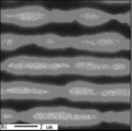
- 5 is a WDX showing a Sn mapping analysis result in Experimental Example 1.
- Experimental Example 3 it is explanatory drawing which shows the location which measured the thickness of the dielectric material layer.
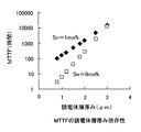
- 10 is a graph showing the dependence of MTTF on the dielectric layer thickness in Experimental Example 3.
- FIG. 1 is a cross-sectional view of a multilayer ceramic capacitor according to the present invention.
- the multilayer ceramic capacitor 1 includes a multilayer body 5.
- the stacked body 5 includes a plurality of stacked dielectric layers 2 and a plurality of internal electrodes 3 and 4 formed along interfaces between the plurality of dielectric layers 2.
- External electrodes 6 and 7 are formed at different positions on the outer surface of the laminate 5. Examples of the material of the external electrodes 6 and 7 include those containing Ag or Cu as a main component. In the multilayer ceramic capacitor shown in FIG. 1, the external electrodes 6 and 7 are formed on the end surfaces of the multilayer body 5 facing each other. The internal electrodes 3 and 4 are electrically connected to the external electrodes 6 and 7, respectively. The internal electrodes 3 and 4 are alternately stacked inside the stacked body 5 via the dielectric layers 2.
- the multilayer ceramic capacitor 1 may be a two-terminal type including two external electrodes 6 and 7 or a multi-terminal type including a large number of external electrodes.
- the internal electrodes 3 and 4 are mainly composed of Ni, and the internal electrodes 3 and 4 contain Sn.
- Sn a multilayer ceramic capacitor having excellent reliability when a voltage is applied can be obtained.
- the presence form of Sn in the internal electrodes 3 and 4 is not limited, but it is preferably present in the form of an alloy of Sn and Ni, and is present in the form of an intermetallic compound of Sn and Ni. Is more preferable. In this case, the insulation at the interface between the dielectric layer 2 and the internal electrodes 3 and 4 is improved, and the reliability at the time of voltage application is further improved.
- the method for containing Sn is not particularly limited.
- it may be contained in the conductive paste to be the internal electrodes 3 and 4 in advance, or may be mixed with the dielectric ceramic raw material powder constituting the dielectric layer 2 after firing.
- SnO powder when SnO powder is mixed with the dielectric ceramic raw material powder and then fired in a reducing atmosphere at a heating rate of 20 ° C./min or more, SnO is reduced to Sn, and the internal electrodes 3 and 4 are formed. It becomes easy to be absorbed.
- the molar ratio of Sn to the total of Ni and Sn is preferably 0.001 or more and less than 0.1.
- Sn is 0.001 or more, the effect of containing Sn becomes more remarkable.
- it is less than 0.1, the melting points of the internal electrodes 3 and 4 are in a preferable range, and problems such as ball formation are less likely to occur.
- the dielectric layer 2 preferably contains a perovskite type compound containing Ba and Ti (provided that a part of Ba may be substituted with Ca and a part of Ti may be substituted with Zr) as a main component.
- the main component of the dielectric layer 2 is BaTiO 3
- the multilayer ceramic capacitor according to the present invention has a high dielectric constant and particularly excellent reliability.
- the dielectric layer may contain, for example, rare earth elements, Mn, Mg, Si, or the like as subcomponents.
- the dielectric ceramic raw material powder is produced by, for example, a solid phase synthesis method. Specifically, first, compound powders such as oxides and carbonates containing the main constituent elements are mixed at a predetermined ratio and calcined. In addition to the solid phase synthesis method, a hydrothermal method or the like may be applied.
- the dielectric ceramic according to the present invention may contain alkali metal, transition metal, Cl, S, P, Hf, etc. in an amount range that does not impede the effects of the present invention.
- the multilayer ceramic capacitor is manufactured as follows, for example.
- a ceramic slurry is prepared using the dielectric ceramic raw material powder obtained as described above. Then, a ceramic green sheet is formed by a sheet forming method or the like. And the electroconductive paste which should become an internal electrode is apply
- Example 1 In Experimental Example 1, the influence of the presence or absence of Sn in the internal electrode on the reliability at the time of voltage application was confirmed. In this experimental example, a method in which SnO powder was mixed in advance with the dielectric ceramic raw material powder was used. In addition, as the main component of the dielectric layer, two kinds of compositions of barium titanate (hereinafter referred to as BT) and barium calcium titanate (hereinafter referred to as BCT) were prepared.
- BT barium titanate
- BCT barium calcium titanate
- BT powder and BCT powder as main components were prepared. Specifically, BaCO 3 powder, CaCO 3 powder, and TiO 2 powder were weighed so that the molar ratio of Ba to Ti was 1-x and the molar ratio of Ca to Ti was x, and mixed by a ball mill for a certain time. Thereafter, heat treatment was performed to obtain main component BT powder and BCT powder.
- R 2 O 3 (R is Dy or Y), MgO, MnO, SiO 2 and SnO, which are subcomponents, were prepared.
- the content of R with respect to 100 mol parts of Ti in the ceramic powder of the main component is a mol parts
- the Mg content is b mol parts
- the Mn content is c mol parts
- the Si content is d. It was weighed so that the mol part and the Sn content would be the e mol part, blended with the main component BT powder and BCT powder, mixed for a certain time by a ball mill, and then dried and dry pulverized.
- dielectric ceramic raw material powders of sample numbers 1 to 8 were obtained. Table 1 shows the values of a, b, c, d, e and x and the R component for each sample number.
- a ceramic green sheet to be a dielectric layer was formed. Specifically, a polyvinyl butyral binder and an organic solvent such as ethanol were added to the above raw material powder, and wet mixed by a ball mill to prepare a ceramic slurry. And this ceramic slurry was shape
- a conductive paste mainly composed of Ni was printed on a predetermined ceramic green sheet to form a conductive paste layer to be an internal electrode.
- this laminate was heated at 350 ° C. in an N 2 atmosphere to burn out the binder. Thereafter, in a reducing atmosphere composed of H 2 —N 2 —H 2 O gas having an oxygen partial pressure of 10 ⁇ 10 MPa, the temperature is raised at a rate of 20 ° C./min and a maximum temperature of 1200 ° C. for 20 minutes, and then the temperature is lowered. Baked with profile.
- the outer dimensions of the multilayer ceramic capacitor fabricated as described above are 2.0 mm ⁇ 1.0 mm ⁇ 1.0 mm, the thickness of the dielectric layer interposed between the internal electrodes is 2.5 ⁇ m, and the thickness of the internal electrodes The thickness was 0.8 ⁇ m.
- the number of effective dielectric layers was 100, and the counter electrode area per layer was 1.7 ⁇ 10 ⁇ 6 m 2 .
- a high-temperature load test was performed under the conditions of 175 ° C. and 7.5 V, the time when the insulation resistance was 100 k ⁇ or less was determined to be a failure, and the average failure time (MTTF) of the sample was calculated. The number of measurements was 10, and the average value was calculated. The dielectric constant, dielectric loss, and MTTF all had 10 measurements, and the average value was calculated.
- Table 1 shows the results of various characteristic evaluations under each condition.
- the sample number with * is a sample outside the scope of the present invention.
- the WT side surface was polished by a polishing machine.
- polishing was finished at a depth of about 1/2 of the L (length) direction of the element body, and a WT cross section was obtained.
- the polished surface was processed by ion milling after the polishing was completed.
- mapping analysis of Ni and Sn was performed by WDX in these four regions.
- a portion near the side portion of the laminated body where the internal electrode does not exist is mapped including the internal electrode, not the central portion.
- FIG. 3 shows the Ni mapping analysis result
- FIG. 4 shows the Sn mapping analysis result of the sample obtained by adding the Sn material powder to the dielectric ceramic raw material powder.
- the inner electrode in the upper region U, the intermediate region M, the lower region D and the side region S Sn was present.
- sample numbers 1 to 4 the main component of the dielectric layer is BT.
- Sample Nos. 1 and 3 containing Sn the dielectric properties were almost the same and the MTTF value was larger than Sample Nos. 2 and 4.
- Sample Nos. 5 to 8 the main component of the dielectric layer is BCT.
- Sample Nos. 5 and 7 containing Sn both had dielectric properties similar to those of Sample Nos. 6 and 8 and a large MTTF value.
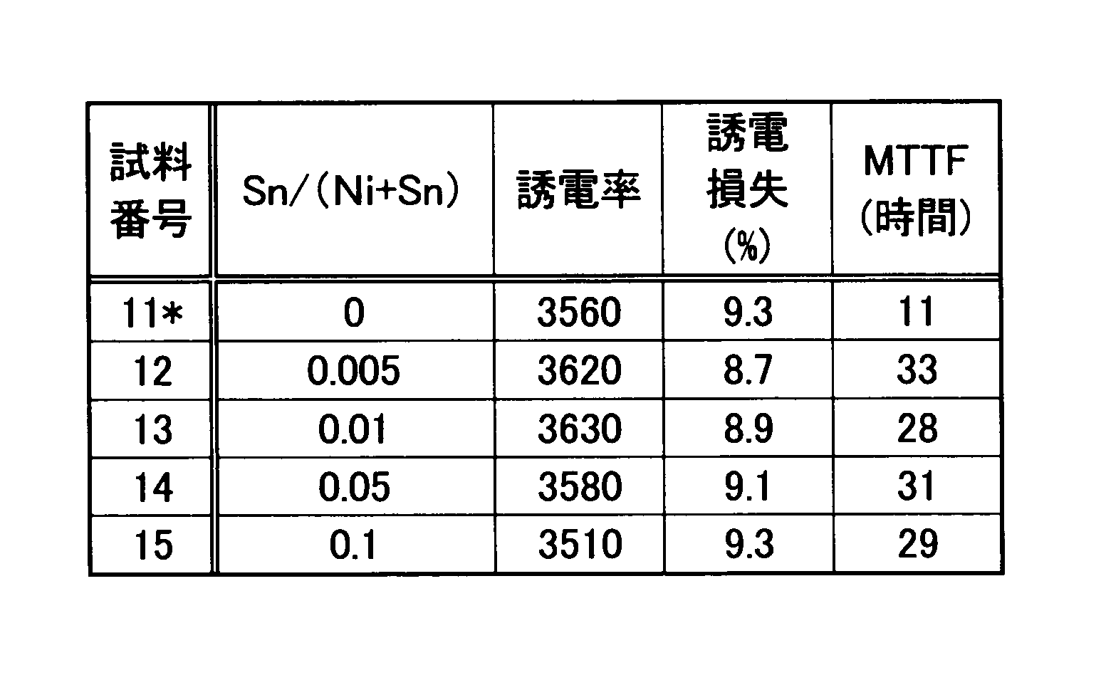
- the sample numbers 12 to 15 When comparing the sample numbers 11 to 15, the sample numbers 12 to 15 all have the same dielectric characteristics and the MTTF value is larger than the sample number 11 that does not contain Sn.
- a BT powder as a main component was prepared. Specifically, BaCO 3 powder and TiO 2 powder were weighed so that the molar ratio of Ti and Ba was 1: 1, mixed for a certain time with a ball mill, and then heat-treated to obtain BT powder as a main component. .
- R 2 O 3 powders of R 2 O 3 (R is Dy), MgO, MnO, SiO 2 and SnO, which are subcomponents, were prepared.
- R is Dy.
- the content of R with respect to 100 mol parts of Ti in the ceramic powder of the main component is a mol parts
- the Mg content is b mol parts
- the Mn content is c mol parts
- the Si content is d.
- dielectric ceramic raw material powders of sample numbers 21 to 36 were obtained.
- Table 3 shows the values of a, b, c, d, and e for each sample number.
- a ceramic green sheet to be a dielectric layer was formed. Specifically, a polyvinyl butyral binder and an organic solvent such as ethanol were added to the above raw material powder, and wet mixed by a ball mill to prepare a ceramic slurry. Then, this ceramic slurry is formed into a sheet shape by a doctor blade method, and ceramic green sheets having eight thicknesses, specifically, 0.9 ⁇ m, 1.1 ⁇ m, 1.3 ⁇ m, 1.6 ⁇ m, 2 Ceramic green sheets having eight thicknesses of 0.0 ⁇ m, 2.2 ⁇ m, 2.7 ⁇ m, and 3.3 ⁇ m were obtained.
- a conductive paste mainly composed of Ni was printed on a predetermined ceramic green sheet to form a conductive paste layer to be an internal electrode.
- this laminate was heated at 350 ° C. in an N 2 atmosphere to burn out the binder. Thereafter, in a reducing atmosphere composed of H 2 —N 2 —H 2 O gas having an oxygen partial pressure of 10 ⁇ 10 MPa, the temperature is raised at a rate of 20 ° C./min and a maximum temperature of 1200 ° C. for 20 minutes, and then the temperature is lowered. Baked with profile.
- the outer dimensions of the multilayer ceramic capacitor produced as described above were 2.0 mm ⁇ 1.0 mm ⁇ 1.0 mm.
- the number of effective dielectric layers was 100, and the counter electrode area per layer was 1.7 ⁇ 10 ⁇ 6 m 2 .
- the external electrodes of the produced multilayer ceramic capacitor were removed, dissolved in a solvent, and analyzed by ICP emission spectroscopy.
- Table 3 shows that the internal electrode components Ni and Sn that diffuse into the internal electrodes are excluded. It was confirmed to be almost the same as the composition shown.
- the thickness of the dielectric layer was examined by the following method.
- each sample was set up vertically and the periphery of each sample was hardened with resin.
- the LT side surface (length / height side surface; the side surface where the internal electrode is exposed including the connecting portion to the external electrode when polished) of each sample was exposed.
- the LT side surface was polished by a polishing machine, and polishing was finished at a depth of 1 ⁇ 2 of the laminated body in the W direction (width direction) to obtain an LT cross section. Ion rimming was performed on the polished surface to remove sagging due to polishing. In this way, a cross section for observation was obtained.
- a perpendicular perpendicular to the internal electrode was drawn in the L direction (length direction) 1/2 of the LT cross section.
- the region where the internal electrodes of the sample were laminated was divided into three equal parts in the T direction (height direction), and divided into three regions, an upper part U, an intermediate part M, and a lower part D.
- 25 dielectric layers are selected from the center in the height direction of each region (a region including the 25 dielectric layers in FIG. 5 is shown as a measurement region R1). The thickness on the perpendicular was measured. However, those that cannot be measured because the internal electrode is missing on the perpendicular line and the dielectric layers sandwiching the internal electrode are connected are excluded from the measurement target.
- the thickness of the dielectric layer was measured at 75 locations for each sample, and the average value thereof was obtained. As shown in Table 3, the thickness of the dielectric layer was 0.8 ⁇ m, 1 ⁇ m, 1.2 ⁇ m, 1.5 ⁇ m, 1.8 ⁇ m, 2 ⁇ m, 2.5 ⁇ m, or 3 ⁇ m depending on the sample.
- a high temperature load test was performed under conditions corresponding to 150 ° C. and 3 V / ⁇ m, and the time when the insulation resistance became 100 k ⁇ or less was determined to be a failure, and the average failure time (MTTF) of the sample was calculated.
- the number of measurements was 10, and the average value was calculated.
- Table 3 shows the results of various characteristic evaluations under each condition.
- the sample number with * is a sample outside the scope of the present invention.
- Sample Nos. 29 to 36 with Sn contained the same dielectric properties and improved MTTF values compared to Sample Nos. 21 to 28 without Sn. However, even when Sn is added, when the thickness of the dielectric layer exceeds 2.5 ⁇ m, specifically, in the sample number 36 with the thickness of the dielectric layer 3, the thickness of the dielectric layer is 2.5 ⁇ m or less. Compared with sample numbers 29 to 35, the rate of improvement in MTTF was reduced.
- FIG. 6 shows the dependence of MTTF on the dielectric layer thickness.
- the region sandwiched between the opposing internal electrodes is composed of “dielectric layer” and “interface between internal electrode and dielectric layer”, but when the thickness of the dielectric layer exceeds 2.5 ⁇ m, The ratio of “dielectric layer” in the region sandwiched between the electrodes increases, and conversely, the ratio of “interface between internal electrode and dielectric layer” decreases.
- the detailed mechanism is unknown, in the present invention, it is considered that the change of the “interface” due to the addition of Sn to the internal electrode contributes to the improvement of the reliability. It is considered that the effect of improving the MTTF is reduced by reducing the ratio of the “interface” when the thickness exceeds 2.5 ⁇ m.
- Example 4 In Experimental Example 4, a method of previously mixing a powder of Sn material with a dielectric ceramic raw material powder was used. Moreover, barium titanate (BT) was prepared as a main component of the dielectric layer.
- BT barium titanate
- a BT powder as a main component was prepared. Specifically, BaCO 3 powder and TiO 2 powder were weighed so that the molar ratio of Ti and Ba was 1: 1, mixed by a ball mill for a certain period of time, and then heat-treated to obtain a main component BT powder. .
- a ceramic green sheet to be a dielectric layer was formed. Specifically, a polyvinyl butyral binder and an organic solvent such as ethanol were added to the above raw material powder, and wet mixed by a ball mill to prepare a ceramic slurry. And this ceramic slurry was shape
- a conductive paste mainly composed of Ni was printed on a predetermined ceramic green sheet to form a conductive paste layer to be an internal electrode.
- this laminate was heated at 350 ° C. in an N 2 atmosphere to burn out the binder. Thereafter, in a reducing atmosphere composed of H 2 —N 2 —H 2 O gas having an oxygen partial pressure of 10 ⁇ 10 MPa, the temperature is raised at a rate of 20 ° C./min and a maximum temperature of 1200 ° C. for 20 minutes, and then the temperature is lowered. Baked with profile.
- the outer dimensions of the multilayer ceramic capacitor fabricated as described above were 2.0 mm ⁇ 1.0 mm ⁇ 1.0 mm, and the thickness of the dielectric layer interposed between the internal electrodes was 2.5 ⁇ m.
- the number of effective dielectric layers was 230, and the counter electrode area per layer was 1.7 ⁇ 10 ⁇ 6 m 2 .
- a high-temperature load test was performed under the conditions of 150 ° C. and 7.5 V, the time when the insulation resistance became 10 k ⁇ or less was determined to be a failure, and the average failure time (MTTF) of the sample was calculated. The number of measurements was 10, and the average value was calculated. The dielectric constant, dielectric loss, and MTTF all had 10 measurements, and the average value was calculated.
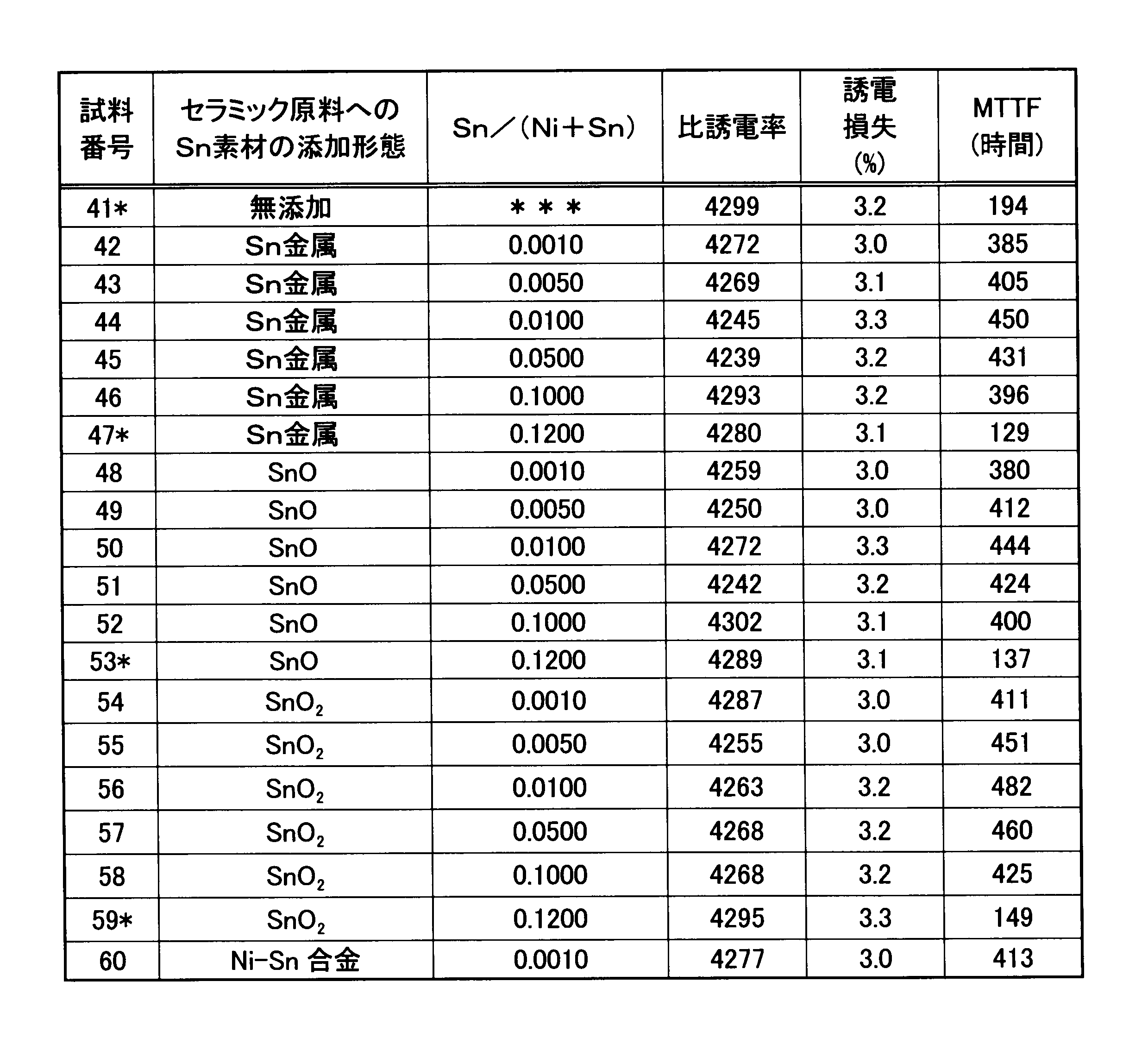
- Table 4 shows the results of various characteristic evaluations under each condition.
- the WT side surface was polished by a polishing machine.
- polishing was finished at a depth of about 1/2 of the L (length) direction of the element body, and a WT cross section was obtained.
- the polished surface was processed by ion milling after polishing.
- 2) Mapping analysis of internal electrode Similar to Experimental Example 1, as shown in FIG. 2, the area where the internal electrode of the sample is laminated is divided into three equal parts in the T direction in about 1 ⁇ 2 of the W direction of the WT cross section. The central part in each W direction was divided into three regions, an upper region U, an intermediate region M, and a lower region D. Further, the central portion in the T direction is divided into two regions: an intermediate region M and a side region S adjacent to the intermediate region M in the W direction.
- mapping analysis of Ni and Sn was performed by WDX in these four regions.
- the side region S a portion near the side portion of the laminated body where the internal electrode does not exist is mapped including the internal electrode, not the central portion.
- Sn was present in the internal electrode in all of the upper region U, the intermediate region M, the lower region D, and the side region S.
- Example 5 In Experimental Example 5, a method of previously mixing the Sn material powder with the internal electrode paste was used. Moreover, barium titanate (BT) was prepared as a main component of the dielectric layer.
- BT barium titanate
- a BT powder as a main component was prepared. Specifically, BaCO 3 powder and TiO 2 powder were weighed so that the molar ratio of Ti and Ba was 1: 1, mixed by a ball mill for a certain period of time, and then heat-treated to obtain a main component BT powder. .
- a ceramic green sheet to be a dielectric layer was formed. Specifically, a polyvinyl butyral binder and an organic solvent such as ethanol were added to the above raw material powder, and wet mixed by a ball mill to prepare a ceramic slurry. And this ceramic slurry was shape
- an internal electrode paste was prepared.
- an organic solvent such as a polyvinyl butyral binder and ethanol was added and wet mixed by a ball mill to prepare a conductive paste.
- the above conductive paste was printed on the above ceramic green sheet to form a conductive paste layer for constituting internal electrodes.
- this laminate was heated at 350 ° C. in an N 2 atmosphere to burn out the binder. Thereafter, in a reducing atmosphere composed of H 2 —N 2 —H 2 O gas having an oxygen partial pressure of 10 ⁇ 10 MPa, the temperature is raised at a rate of 20 ° C./min and a maximum temperature of 1200 ° C. for 20 minutes, and then the temperature is lowered. Baked with profile.
- the outer dimensions of the multilayer ceramic capacitor fabricated as described above were 2.0 mm ⁇ 1.0 mm ⁇ 1.0 mm, and the thickness of the dielectric layer interposed between the internal electrodes was 2.5 ⁇ m.
- the number of effective dielectric layers was 230, and the counter electrode area per layer was 1.7 ⁇ 10 ⁇ 6 m 2 .
- a high-temperature load test was performed under the conditions of 150 ° C. and 7.5 V, the time when the insulation resistance became 10 k ⁇ or less was determined to be a failure, and the average failure time (MTTF) of the sample was calculated. The number of measurements was 10, and the average value was calculated. The dielectric constant, dielectric loss, and MTTF all had 10 measurements, and the average value was calculated.
- Table 5 shows the results of various characteristic evaluations under each condition.
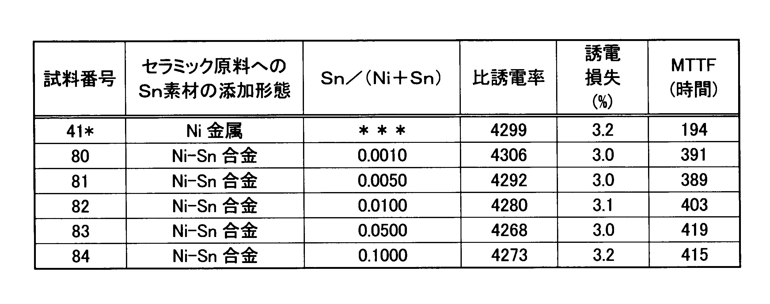
- Example 6 In Experimental Example 6, a method using a Ni—Sn alloy as a metal powder for the internal electrode paste was used. Moreover, barium titanate (BT) was prepared as a main component of the dielectric layer.
- BT barium titanate
- a BT powder as a main component was prepared. Specifically, BaCO 3 powder and TiO 2 powder were weighed so that the molar ratio of Ti and Ba was 1: 1, mixed by a ball mill for a certain period of time, and then heat-treated to obtain a main component BT powder. .
- a ceramic green sheet to be a dielectric layer was formed. Specifically, a polyvinyl butyral binder and an organic solvent such as ethanol were added to the above raw material powder, and wet mixed by a ball mill to prepare a ceramic slurry. And this ceramic slurry was shape
- Ni—Sn alloy powder As metal powder was prepared.
- An Ni—Sn alloy powder having a Sn / (Ni + Sn) ratio shown in Table 6 was prepared, an organic solvent such as a polyvinyl butyral binder and ethanol was added, and wet mixed by a ball mill to prepare a conductive paste.
- the above conductive paste was printed on the above ceramic green sheet to form a conductive paste layer for constituting internal electrodes.
- this laminate was heated at 350 ° C. in an N 2 atmosphere to burn out the binder. Thereafter, in a reducing atmosphere composed of H 2 —N 2 —H 2 O gas having an oxygen partial pressure of 10 ⁇ 10 MPa, the temperature is raised at a rate of 20 ° C./min and a maximum temperature of 1200 ° C. for 20 minutes, and then the temperature is lowered. Baked with profile.
- the outer dimensions of the multilayer ceramic capacitor fabricated as described above were 2.0 mm ⁇ 1.0 mm ⁇ 1.0 mm, and the thickness of the dielectric layer interposed between the internal electrodes was 2.5 ⁇ m.
- the number of effective dielectric layers was 230, and the counter electrode area per layer was 1.7 ⁇ 10 ⁇ 6 m 2 .
- a high-temperature load test was performed under the conditions of 150 ° C. and 7.5 V, the time when the insulation resistance became 10 k ⁇ or less was determined to be a failure, and the average failure time (MTTF) of the sample was calculated. The number of measurements was 10, and the average value was calculated. The dielectric constant, dielectric loss, and MTTF all had 10 measurements, and the average value was calculated.
- Table 6 shows the results of various characteristic evaluations under each condition.
Landscapes
- Engineering & Computer Science (AREA)
- Power Engineering (AREA)
- Chemical & Material Sciences (AREA)
- Ceramic Engineering (AREA)
- Manufacturing & Machinery (AREA)
- Microelectronics & Electronic Packaging (AREA)
- Inorganic Chemistry (AREA)
- Materials Engineering (AREA)
- Ceramic Capacitors (AREA)
- Fixed Capacitors And Capacitor Manufacturing Machines (AREA)
Abstract
Description
実験例1では、内部電極中のSnの有無が電圧印加時の信頼性に与える影響を確認した。なお、本実験例では、誘電体セラミックの原料粉末にSnO粉末をあらかじめ混合する方法を用いた。また、誘電体層の主成分としては、チタン酸バリウム(以下BT)とチタン酸バリウムカルシウム(以下BCT)の2種類の組成を用意した。
最初に、主成分であるBT粉末とBCT粉末を用意した。具体的には、BaCO3粉末、CaCO3粉末、及びTiO2粉末をTiに対するBaのモル比が1-x、Tiに対するCaのモル比がxとなるように秤量し、ボールミルにより一定時間混合した後、熱処理を行い、主成分のBT粉末とBCT粉末を得た。
最初に、誘電体層となるべきセラミックグリーンシートを形成した。具体的には、上記の原料粉末に、ポリビニルブチラール系バインダと、エタノール等の有機溶媒を加えて、ボールミルにより湿式混合してセラミックスラリーを調製した。そして、このセラミックスラリーを、ドクターブレード法によりシート状に成形して、厚さが3μmのセラミックグリーンシートを得た。
得られた各条件の積層セラミックコンデンサについて、誘電率と誘電損失を測定した。最初に、自動ブリッジ式測定器を用いて、静電容量と誘電損失をAC電圧1V、1kHzの条件で測定した。そして、静電容量の平均値と誘電体層の厚さ、層数、対向電極面積から、誘電率を算出した。
1)研磨
各試料を垂直になるように立てて、各試料の周りを樹脂で固めた。このとき、各試料のWT(幅・高さ)側面が露出するようにした。
図2に示す通り、WT断面のW方向1/2程度において、試料の内部電極が積層されている領域をT方向に3等分に分割し、それぞれのW方向における中央部を上方領域U、中間領域M、下方領域Dの3つの領域に分けた。さらに、T方向の中央部は、中間領域Mと、中間領域MからW方向に隣接する側部領域Sの2つの領域に分けた。
誘電体セラミックの原料粉末にSn素材粉末を入れた試料(資料番号1、3、5、7)につき、内部電極中のSn/(Ni+Sn)値を確認した。具体的には、1つの積層セラミックコンデンサから無作為に3本の内部電極を選び、FIB加工(集束イオンビーム法)にてそれぞれ内部電極部のみを切り出して薄片化した試料を3個用意した。各試料に対して無作為に抽出した10箇所でNiとSnの定量分析をWDXを用いて実施した。合計30箇所(10箇所×3個)の平均値を調べたところ、各試料とも、Sn/(Ni+Sn)=0.006であった。
焼成後の積層セラミックコンデンサ(積層体)を粉砕し、粉末状にした。その粉末をXRDで分析したところ、Niのピーク位置がシフトしていた。このことから、内部電極中のSnはNiとSnの合金の形成で存在していることが分かった。

実験例2では、内部電極中のSnの量が電圧印加時の信頼性に与える影響を確認した。なお、本実験例では、内部電極となるべき導電性ペーストに、主成分としてNiとSnの合金が含まれているものを用いた。また、誘電体セラミックには、実験例1の試料番号6と同じ条件のものを用いた。積層セラミックコンデンサの作製方法は実験例1と同様である。作製した積層セラミックコンデンサの内部電極間に介在する誘電体層の厚さは2.5μmであった。表2に、各試料番号の条件における、内部電極中の、NiとSnの合計に対するSnのモル比と、各種特性評価の結果を示す。
実験例3では、誘電体層の厚みを変化させ、MTTFに与える影響を調べた。なお、本実験例では、誘電体セラミックの原料粉末にSnO粉末をあらかじめ混合する方法を用いた。また、誘電体層の主成分は、チタン酸バリウム(BT)とした。
最初に、主成分であるBT粉末を用意した。具体的には、BaCO3粉末及びTiO2粉末をTiとBaのモル比が1:1となるように秤量し、ボールミルにより一定時間混合した後、熱処理を行い、主成分のBT粉末を得た。
最初に、誘電体層となるべきセラミックグリーンシートを形成した。具体的には、上記の原料粉末にポリビニルブチラール系バインダと、エタノール等の有機溶媒を加えて、ボールミルにより湿式混合してセラミックスラリーを調製した。そして、このセラミックスラリーを、ドクターブレード法によりシート状に成形して、8種類の厚さのセラミックグリーンシート、具体的には、0.9μm、1.1μm、1.3μm、1.6μm、2.0μm、2.2μm、2.7μm、3.3μmの8種類の厚さのセラミックグリーンシートを得た。
得られた各条件の積層セラミックコンデンサについて、誘電率と誘電損失を測定した。最初に、自動ブリッジ式測定器を用いて、静電容量と誘電損失をAC電圧1V、1kHzの条件で測定した。そして、静電容量の平均値と誘電体層の厚さ、層数、対向電極面積から、誘電率を算出した。
実験例1と同様の方法により、各試料について、WDXによりNiおよびSnのマッピング分析結果をおこなった。その結果、誘電体セラミックの原料粉末にSn素材粉末を入れた試料では、内部電極中にSnが存在していた。
誘電体セラミックの原料粉末にSn素材粉末を入れた試料につき、内部電極中のSn/(Ni+Sn)値を確認した。具体的には、1つのチップから無作為に3本の内部電極を選び、FIB加工(集束イオンビーム法)にてそれぞれ内部電極部のみを切り出して薄片化した試料を3個用意した。各試料に対して無作為に抽出した10箇所でNiとSnの定量分析をWDXを用いて実施した。合計30箇所(10箇所×3個)の平均値が表3に示したSn/(Ni+Sn)である。
また、積層セラミックコンデンサの外部電極を除去した後、これを粉砕し、粉末状にした。その粉末をXRDで測定したところ、Niのピーク位置がシフトしていたことから、本実験例では、内部電極中のSnはNiとSnの合金の形で存在していることが分かった。

実験例4では、誘電体セラミックの原料粉末にSn素材の粉末をあらかじめ混合する方法を用いた。また、誘電体層の主成分としては、チタン酸バリウム(BT)を用意した。
最初に、主成分であるBT粉末を用意した。具体的には、BaCO3粉末及びTiO2粉末をTiとBaのモル比が1:1となるように秤量し、ボールミルにより一定時間混合した後、熱処理を行い、主成分のBT粉末を得た。
最初に、誘電体層となるべきセラミックグリーンシートを形成した。具体的には、上記の原料粉末に、ポリビニルブチラール系バインダと、エタノール等の有機溶媒を加えて、ボールミルにより湿式混合してセラミックスラリーを調製した。そして、このセラミックスラリーを、ドクターブレード法によりシート状に成形して、厚さが3μmのセラミックグリーンシートを得た。
得られた各条件の積層セラミックコンデンサについて、誘電率と誘電損失を測定した。最初に、自動ブリッジ式測定器を用いて、静電容量と誘電損失をAC電圧1V、1kHzの条件で測定した。そして、静電容量の平均値と誘電体層の厚さ、層数、対向電極面積から、誘電率を算出した。
1)研磨
各試料を垂直になるように立てて、各試料の周りを樹脂で固めた。このとき、各試料のWT(幅・高さ)側面が露出するようにした。
2)内部電極のマッピング分析
実験例1と同様に、図2に示すように、WT断面のW方向1/2程度において、試料の内部電極が積層されている領域をT方向に3等分に分割し、それぞれのW方向における中央部を上方領域U、中間領域M、下方領域Dの3つの領域に分けた。さらに、T方向の中央部は、中間領域Mと、中間領域MからW方向に隣接する側部領域Sの2つの領域に分けた。
誘電体セラミックの原料粉末にSn素材粉末を入れた試料につき、内部電極中のSn/(Ni+Sn)値を確認した。具体的には、1つの積層セラミックコンデンサから無作為に3本の内部電極を選び、FIB加工(集束イオンビーム法)にてそれぞれ内部電極部のみを切り出して薄片化した試料を3個用意した。各試料に対して無作為に抽出した10箇所でNiとSnの定量分析をWDXを用いて実施した。合計30箇所(10箇所×3個)の平均値が表4に示したSn/(Ni+Sn)である。
焼成後の積層セラミックコンデンサ(積層体)を粉砕し、粉末状にした。その粉末をXRDで分析したところ、Niのピーク位置がシフトしていた。このことから、内部電極中のSnはNiとSnの合金の形成で存在していることが分かった。
実験例5では、内部電極ペーストにSn素材の粉末をあらかじめ混合する方法を用いた。また、誘電体層の主成分としては、チタン酸バリウム(BT)を用意した。
最初に、主成分であるBT粉末を用意した。具体的には、BaCO3粉末及びTiO2粉末をTiとBaのモル比が1:1となるように秤量し、ボールミルにより一定時間混合した後、熱処理を行い、主成分のBT粉末を得た。
最初に、誘電体層となるべきセラミックグリーンシートを形成した。具体的には、上記の原料粉末に、ポリビニルブチラール系バインダと、エタノール等の有機溶媒を加えて、ボールミルにより湿式混合してセラミックスラリーを調製した。そして、このセラミックスラリーを、ドクターブレード法によりシート状に成形して、厚さが3μmのセラミックグリーンシートを得た。
得られた各条件の積層セラミックコンデンサについて、誘電率と誘電損失を測定した。最初に、自動ブリッジ式測定器を用いて、静電容量と誘電損失をAC電圧1V、1kHzの条件で測定した。そして、静電容量の平均値と誘電体層の厚さ、層数、対向電極面積から、誘電率を算出した。
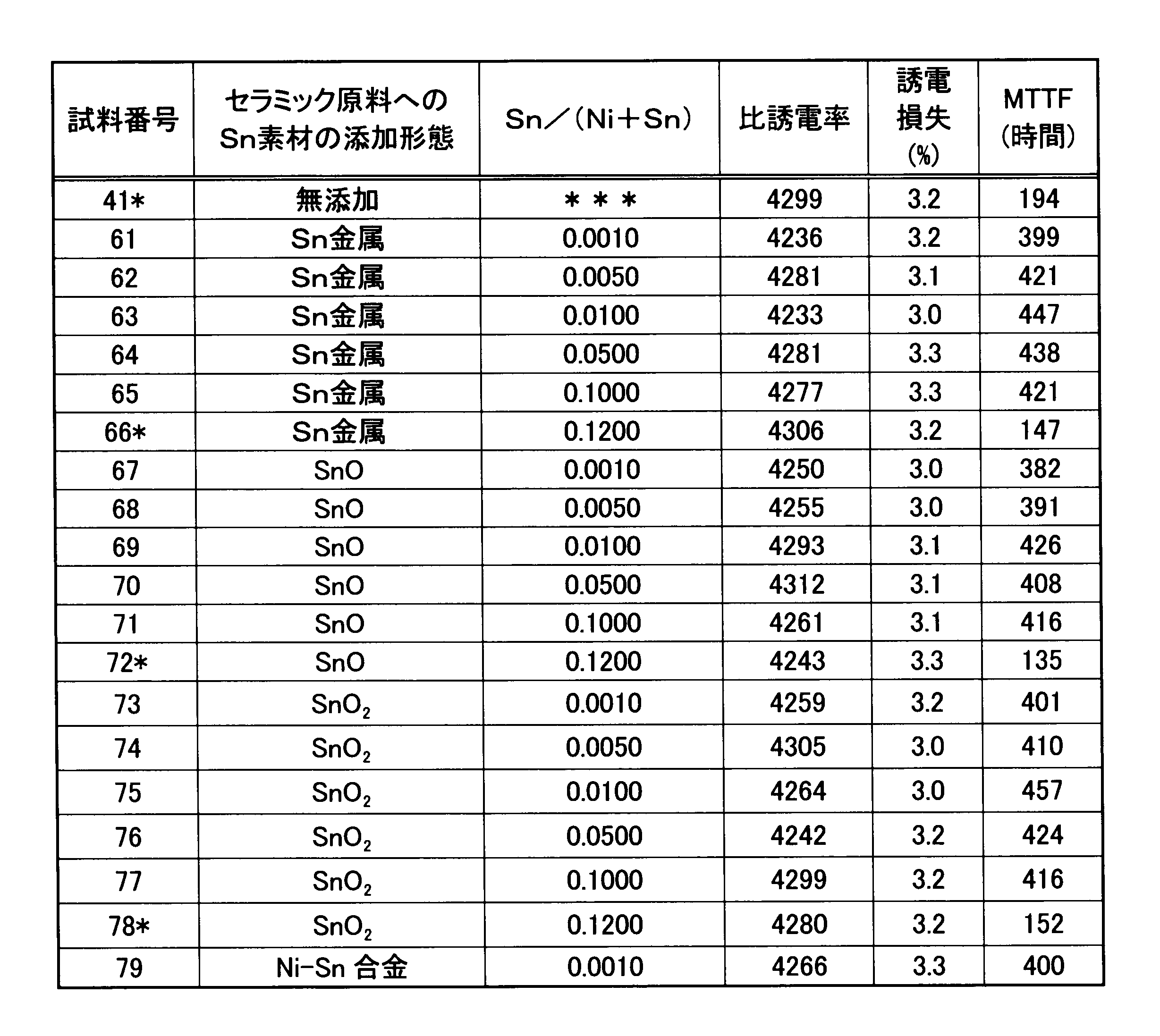
実験例6では、内部電極ペーストに金属粉末としてNi-Sn合金を使用する方法方法を用いた。また、誘電体層の主成分としては、チタン酸バリウム(BT)を用意した。
最初に、主成分であるBT粉末を用意した。具体的には、BaCO3粉末及びTiO2粉末をTiとBaのモル比が1:1となるように秤量し、ボールミルにより一定時間混合した後、熱処理を行い、主成分のBT粉末を得た。
最初に、誘電体層となるべきセラミックグリーンシートを形成した。具体的には、上記の原料粉末に、ポリビニルブチラール系バインダと、エタノール等の有機溶媒を加えて、ボールミルにより湿式混合してセラミックスラリーを調製した。そして、このセラミックスラリーを、ドクターブレード法によりシート状に成形して、厚さが3μmのセラミックグリーンシートを得た。
得られた各条件の積層セラミックコンデンサについて、誘電率と誘電損失を測定した。最初に、自動ブリッジ式測定器を用いて、静電容量と誘電損失をAC電圧1V、1kHzの条件で測定した。そして、静電容量の平均値と誘電体層の厚さ、層数、対向電極面積から、誘電率を算出した。
2 誘電体層
3、4 内部電極
5 積層体
6、7 外部電極
Claims (5)
- 積層されている複数の誘電体層と、前記誘電体層間の界面に沿って形成されている複数の内部電極と、を有する積層体と、前記積層体の外表面に形成され、前記内部電極と電気的に接続されている複数の外部電極と、を備える積層セラミックコンデンサにおいて、
前記誘電体層の厚みは2.5μm以下であり、
前記内部電極は主成分がNiであり、かつ、前記内部電極はSnを含み、前記内部電極における、前記Niと前記Snの合計に対する前記Snのモル比が0.001以上0.1以下であることを特徴とする積層セラミックコンデンサ。 - 前記誘電体層が、BaおよびTiを含むペロブスカイト型化合物(ただし、Baの一部はCaで置換されても良く、Tiの一部はZrで置換されても良い)を主成分として含むことを特徴とする、請求項1に記載の積層セラミックコンデンサ。
- ぺロブスカイト型化合物を主成分とする主成分粉末を用意する工程と、
Sn金属、Snを含む合金、Sn化合物のいずれかからなるSn素材の中から、少なくとも1つを用意する工程と、
前記用意した主成分粉末および前記用意したSn素材を含有するセラミックグリーンシートを得る工程と、
前記セラミックグリーンシートと、内部電極層とを積み重ねて焼成前の積層体を得る工程と、
前記焼成前の積層体を焼成して、積層体を得る工程と、を備える、複数の誘電体層と、当該誘電体層間の界面に沿って形成されている複数の内部電極と、を有する積層セラミックコンデンサの製造方法であって、
前記内部電極は主成分としてNiを含み、かつ、前記内部電極はSnを含み、前記内部電極における、前記Niと前記Snの合計に対する前記Snのモル比が0.001以上0.1以下であることを特徴とする、積層セラミックコンデンサの製造方法。 - Ni金属もしくはNiを含む合金を主成分とする内部電極主成分粉末を用意する工程と、
Sn金属、Snを含む合金、Sn化合物のいずれかからなるSn素材の中から、少なくとも1つを用意する工程と、
ぺロブスカイト型化合物を主成分とする主成分粉末を含有するセラミックグリーンシートを得る工程と、
前記セラミックグリーンシートと、前記用意した内部電極主成分粉末および前記用意したSn素材を含有する内部電極層と、を積み重ねて焼成前の積層体を得る工程と、
前記焼成前の積層体を焼成して、積層体を得る工程と、を備える、複数の誘電体層と、当該誘電体層間の界面に沿って形成されている複数の内部電極と、を有する積層セラミックコンデンサの製造方法であって、
前記内部電極は主成分としてNiを含み、かつ、前記内部電極はSnを含み、前記内部電極における、NiとSnの合計に対するSnのモル比が0.001以上0.1以下であることを特徴とする、積層セラミックコンデンサの製造方法。 - Ni-Sn合金を主成分とする内部電極主成分粉末を用意する工程と、
ぺロブスカイト型化合物を主成分とする主成分粉末を含有するセラミックグリーンシートを得る工程と、
前記セラミックグリーンシートと、前記用意した内部電極主成分粉末を含有する内部電極層と、を積み重ねて焼成前の積層体を得る工程と、
前記焼成前の積層体を焼成して、積層体を得る工程と、を備える、複数の誘電体層と、当該誘電体層間の界面に沿って形成されている複数の内部電極と、を有する積層セラミックコンデンサの製造方法であって、
前記内部電極は主成分としてNiを含み、かつ、前記内部電極はSnを含み、前記内部電極における、NiとSnの合計に対するSnのモル比が0.001以上0.1以下であることを特徴とする、積層セラミックコンデンサの製造方法。
Priority Applications (5)
| Application Number | Priority Date | Filing Date | Title |
|---|---|---|---|
| JP2012557941A JP5488725B2 (ja) | 2011-02-14 | 2012-02-13 | 積層セラミックコンデンサの製造方法 |
| CN201280008834.6A CN103370755B (zh) | 2011-02-14 | 2012-02-13 | 层叠陶瓷电容器及层叠陶瓷电容器的制造方法 |
| KR1020137021240A KR101581925B1 (ko) | 2011-02-14 | 2012-02-13 | 적층 세라믹 콘덴서 및 적층 세라믹 콘덴서의 제조방법 |
| DE112012000798.0T DE112012000798B4 (de) | 2011-02-14 | 2012-02-13 | Verfahren zum Herstellen eines mehrschichtigen Keramikkondensators |
| US13/963,086 US9099244B2 (en) | 2011-02-14 | 2013-08-09 | Multilayer ceramic capacitor and method for manufacturing multilayer ceramic capacitor |
Applications Claiming Priority (2)
| Application Number | Priority Date | Filing Date | Title |
|---|---|---|---|
| JP2011028981 | 2011-02-14 | ||
| JP2011-028981 | 2011-02-14 |
Related Child Applications (1)
| Application Number | Title | Priority Date | Filing Date |
|---|---|---|---|
| US13/963,086 Continuation US9099244B2 (en) | 2011-02-14 | 2013-08-09 | Multilayer ceramic capacitor and method for manufacturing multilayer ceramic capacitor |
Publications (1)
| Publication Number | Publication Date |
|---|---|
| WO2012111592A1 true WO2012111592A1 (ja) | 2012-08-23 |
Family
ID=46672511
Family Applications (1)
| Application Number | Title | Priority Date | Filing Date |
|---|---|---|---|
| PCT/JP2012/053233 Ceased WO2012111592A1 (ja) | 2011-02-14 | 2012-02-13 | 積層セラミックコンデンサ及び積層セラミックコンデンサの製造方法 |
Country Status (6)
| Country | Link |
|---|---|
| US (1) | US9099244B2 (ja) |
| JP (2) | JP5488725B2 (ja) |
| KR (1) | KR101581925B1 (ja) |
| CN (1) | CN103370755B (ja) |
| DE (1) | DE112012000798B4 (ja) |
| WO (1) | WO2012111592A1 (ja) |
Cited By (14)
| Publication number | Priority date | Publication date | Assignee | Title |
|---|---|---|---|---|
| JP2013157460A (ja) * | 2012-01-30 | 2013-08-15 | Tdk Corp | 積層セラミックコンデンサ |
| WO2014024592A1 (ja) * | 2012-08-07 | 2014-02-13 | 株式会社村田製作所 | 積層セラミックコンデンサおよび積層セラミックコンデンサの製造方法 |
| WO2014024538A1 (ja) * | 2012-08-07 | 2014-02-13 | 株式会社村田製作所 | 積層セラミックコンデンサおよび積層セラミックコンデンサの製造方法 |
| WO2015016309A1 (ja) * | 2013-08-02 | 2015-02-05 | 株式会社村田製作所 | 積層セラミックコンデンサおよび積層セラミックコンデンサの製造方法 |
| WO2015087688A1 (ja) * | 2013-12-10 | 2015-06-18 | 株式会社村田製作所 | 積層セラミックコンデンサおよび積層セラミックコンデンサの製造方法 |
| JP2017005019A (ja) * | 2015-06-05 | 2017-01-05 | 株式会社村田製作所 | 積層セラミックコンデンサおよび積層セラミックコンデンサの製造方法 |
| JP2021015965A (ja) * | 2019-07-15 | 2021-02-12 | サムソン エレクトロ−メカニックス カンパニーリミテッド. | キャパシタ部品 |
| KR20210084284A (ko) * | 2019-12-27 | 2021-07-07 | 가부시키가이샤 무라타 세이사쿠쇼 | 적층 세라믹 콘덴서 |
| KR20210084536A (ko) | 2018-10-31 | 2021-07-07 | 쇼에이 가가쿠 가부시키가이샤 | Ni 페이스트 및 적층 세라믹 콘덴서 |
| JP2021108360A (ja) * | 2019-12-27 | 2021-07-29 | 株式会社村田製作所 | 積層セラミックコンデンサ |
| JP2022109873A (ja) * | 2021-01-15 | 2022-07-28 | サムソン エレクトロ-メカニックス カンパニーリミテッド. | 積層型キャパシター |
| KR20220130024A (ko) * | 2021-03-17 | 2022-09-26 | 가부시키가이샤 무라타 세이사쿠쇼 | 적층 세라믹 콘덴서 |
| JPWO2022210628A1 (ja) * | 2021-03-31 | 2022-10-06 | ||
| CN115458329A (zh) * | 2018-08-23 | 2022-12-09 | 三星电机株式会社 | 多层陶瓷电子组件 |
Families Citing this family (28)
| Publication number | Priority date | Publication date | Assignee | Title |
|---|---|---|---|---|
| KR101537717B1 (ko) * | 2013-09-17 | 2015-07-20 | 신유선 | 임베디드용 적층 세라믹 캐패시터 및 임베디드용 적층 세라믹 캐패시터의 제조 방법 |
| TWI642074B (zh) * | 2016-06-06 | 2018-11-21 | 村田製作所股份有限公司 | Multilayer ceramic capacitor |
| US10770227B2 (en) | 2017-11-22 | 2020-09-08 | Samsung Electro-Mechanics Co., Ltd. | Capacitor and board having the same |
| KR102107027B1 (ko) | 2017-11-22 | 2020-05-07 | 삼성전기주식회사 | 커패시터 및 그 실장기판 |
| KR102407983B1 (ko) * | 2018-08-23 | 2022-06-13 | 삼성전기주식회사 | 적층 세라믹 전자부품 및 그 제조방법 |
| KR102789045B1 (ko) * | 2018-10-17 | 2025-04-01 | 삼성전기주식회사 | 적층 세라믹 전자부품 및 그 제조방법 |
| JP7348890B2 (ja) * | 2020-10-30 | 2023-09-21 | 太陽誘電株式会社 | セラミック電子部品およびその製造方法 |
| JP7396251B2 (ja) * | 2020-11-11 | 2023-12-12 | 株式会社村田製作所 | 積層セラミックコンデンサ |
| KR102776258B1 (ko) | 2020-11-16 | 2025-03-07 | 삼성전기주식회사 | 전자 부품 및 그 제조 방법 |
| JP2022083829A (ja) * | 2020-11-25 | 2022-06-06 | 株式会社村田製作所 | 積層セラミックコンデンサ |
| KR102803432B1 (ko) * | 2020-12-11 | 2025-05-07 | 삼성전기주식회사 | 적층형 전자 부품 |
| KR102921396B1 (ko) | 2021-01-12 | 2026-02-02 | 삼성전기주식회사 | 적층형 전자 부품 |
| US12073996B2 (en) * | 2021-03-01 | 2024-08-27 | Taiyo Yuden Co., Ltd. | Ceramic electronic device, powder material, paste material, and manufacturing method of ceramic electronic device |
| JP7767020B2 (ja) * | 2021-03-31 | 2025-11-11 | 太陽誘電株式会社 | セラミック電子部品およびその製造方法 |
| KR20230057174A (ko) * | 2021-10-21 | 2023-04-28 | 삼성전기주식회사 | 세라믹 전자부품 |
| KR102894865B1 (ko) * | 2021-10-21 | 2025-12-04 | 삼성전기주식회사 | 세라믹 전자부품 |
| JP7616431B2 (ja) * | 2021-12-23 | 2025-01-17 | 株式会社村田製作所 | 電子部品 |
| JP7459858B2 (ja) * | 2021-12-23 | 2024-04-02 | 株式会社村田製作所 | 積層セラミックコンデンサおよび積層セラミックコンデンサの実装構造 |
| KR102881364B1 (ko) | 2021-12-28 | 2025-11-04 | 삼성전기주식회사 | 적층 세라믹 커패시터 |
| KR20230099932A (ko) | 2021-12-28 | 2023-07-05 | 삼성전기주식회사 | 적층형 전자 부품 |
| JP2023132182A (ja) | 2022-03-10 | 2023-09-22 | 太陽誘電株式会社 | セラミック電子部品およびその製造方法 |
| WO2023234392A1 (ja) * | 2022-06-03 | 2023-12-07 | 京セラ株式会社 | 積層セラミックコンデンサ |
| JP2024055118A (ja) * | 2022-10-06 | 2024-04-18 | 太陽誘電株式会社 | セラミック電子部品およびその製造方法 |
| US12488944B2 (en) | 2022-11-04 | 2025-12-02 | Samsung Electro-Mechanics Co., Ltd. | Multilayer electronic component |
| CN118073095A (zh) | 2022-11-24 | 2024-05-24 | 国巨电子(中国)有限公司 | 积层陶瓷电容及其制作方法 |
| KR20240106561A (ko) | 2022-12-29 | 2024-07-08 | 삼성전기주식회사 | 적층형 전자 부품 |
| JP2025007690A (ja) * | 2023-07-03 | 2025-01-17 | 株式会社村田製作所 | 積層セラミックコンデンサ |
| JP2025007685A (ja) * | 2023-07-03 | 2025-01-17 | 株式会社村田製作所 | 積層セラミックコンデンサ |
Citations (4)
| Publication number | Priority date | Publication date | Assignee | Title |
|---|---|---|---|---|
| JP2000124058A (ja) * | 1999-09-06 | 2000-04-28 | Tdk Corp | 積層型セラミックチップコンデンサ |
| JP2000348962A (ja) * | 1999-03-31 | 2000-12-15 | Tdk Corp | 誘電体組成物及びこれを用いたセラミックコンデンサ |
| JP2005298315A (ja) * | 2004-04-14 | 2005-10-27 | Samsung Electro Mech Co Ltd | 耐還元性誘電体磁器組成物と超薄層積層セラミックコンデンサ |
| WO2010146967A1 (ja) * | 2009-06-15 | 2010-12-23 | 株式会社村田製作所 | 積層セラミック電子部品およびその製造方法 |
Family Cites Families (18)
| Publication number | Priority date | Publication date | Assignee | Title |
|---|---|---|---|---|
| JPS5954672A (ja) | 1982-09-22 | 1984-03-29 | 株式会社村田製作所 | 高誘電率磁器の製造方法 |
| JPS59126354A (ja) * | 1982-12-22 | 1984-07-20 | Fujitsu Ltd | 電話機のハンドセツト |
| JPH04110978A (ja) | 1990-08-31 | 1992-04-13 | Mita Ind Co Ltd | 画像形成装置 |
| JP2680480B2 (ja) * | 1991-01-30 | 1997-11-19 | 太陽誘電 株式会社 | 積層セラミックコンデンサ |
| JPH05290622A (ja) | 1992-04-09 | 1993-11-05 | Sumitomo Metal Mining Co Ltd | Niペースト組成物 |
| JP3552878B2 (ja) | 1997-05-30 | 2004-08-11 | Fdk株式会社 | 低温焼結誘電体磁器の製造方法 |
| JP3874041B2 (ja) * | 1997-08-18 | 2007-01-31 | Tdk株式会社 | Cr複合電子部品とその製造方法 |
| JPH11283867A (ja) | 1998-03-31 | 1999-10-15 | Tdk Corp | 電子部品およびその製造方法 |
| US6291380B1 (en) * | 1999-03-15 | 2001-09-18 | Rohm Co., Ltd. | Dielectric ceramic and capacitor using the same |
| CA2359347A1 (en) * | 2001-10-18 | 2003-04-18 | Cesur Celik | Laminated ceramic capacitor internal electrode material |
| JP4110978B2 (ja) * | 2003-01-24 | 2008-07-02 | 株式会社村田製作所 | 誘電体セラミックおよびその製造方法ならびに積層セラミックコンデンサ |
| TW200705481A (en) | 2005-04-28 | 2007-02-01 | Tdk Corp | Method of production of multilayer ceramic electronic device |
| DE112007001335B4 (de) * | 2006-07-07 | 2019-05-23 | Murata Manufacturing Co., Ltd. | Dielektrische Keramik, Keramikelektronikelement und Vielschicht-Keramikkondensator |
| DE112007002865B4 (de) * | 2006-12-05 | 2018-03-01 | Murata Manufacturing Co., Ltd. | Dielektrische Keramik und diese verwendender Mehrschicht-Keramikkondensator |
| CN101595533B (zh) * | 2007-02-06 | 2012-07-18 | 株式会社村田制作所 | 电阻糊剂及层叠陶瓷电容器 |
| WO2008099772A1 (ja) * | 2007-02-14 | 2008-08-21 | Murata Manufacturing Co., Ltd. | 積層セラミックコンデンサおよびその製造方法 |
| JP5315796B2 (ja) * | 2007-06-18 | 2013-10-16 | 株式会社村田製作所 | 積層セラミックコンデンサ |
| JP4992955B2 (ja) * | 2009-11-20 | 2012-08-08 | 株式会社村田製作所 | 誘電体セラミックおよび積層セラミックコンデンサ |
-
2012
- 2012-02-13 DE DE112012000798.0T patent/DE112012000798B4/de active Active
- 2012-02-13 KR KR1020137021240A patent/KR101581925B1/ko active Active
- 2012-02-13 CN CN201280008834.6A patent/CN103370755B/zh active Active
- 2012-02-13 WO PCT/JP2012/053233 patent/WO2012111592A1/ja not_active Ceased
- 2012-02-13 JP JP2012557941A patent/JP5488725B2/ja active Active
-
2013
- 2013-08-09 US US13/963,086 patent/US9099244B2/en active Active
- 2013-11-22 JP JP2013241458A patent/JP5757319B2/ja active Active
Patent Citations (4)
| Publication number | Priority date | Publication date | Assignee | Title |
|---|---|---|---|---|
| JP2000348962A (ja) * | 1999-03-31 | 2000-12-15 | Tdk Corp | 誘電体組成物及びこれを用いたセラミックコンデンサ |
| JP2000124058A (ja) * | 1999-09-06 | 2000-04-28 | Tdk Corp | 積層型セラミックチップコンデンサ |
| JP2005298315A (ja) * | 2004-04-14 | 2005-10-27 | Samsung Electro Mech Co Ltd | 耐還元性誘電体磁器組成物と超薄層積層セラミックコンデンサ |
| WO2010146967A1 (ja) * | 2009-06-15 | 2010-12-23 | 株式会社村田製作所 | 積層セラミック電子部品およびその製造方法 |
Cited By (37)
| Publication number | Priority date | Publication date | Assignee | Title |
|---|---|---|---|---|
| JP2013157460A (ja) * | 2012-01-30 | 2013-08-15 | Tdk Corp | 積層セラミックコンデンサ |
| JP2016174188A (ja) * | 2012-08-07 | 2016-09-29 | 株式会社村田製作所 | 積層セラミックコンデンサおよび積層セラミックコンデンサの製造方法 |
| WO2014024592A1 (ja) * | 2012-08-07 | 2014-02-13 | 株式会社村田製作所 | 積層セラミックコンデンサおよび積層セラミックコンデンサの製造方法 |
| WO2014024538A1 (ja) * | 2012-08-07 | 2014-02-13 | 株式会社村田製作所 | 積層セラミックコンデンサおよび積層セラミックコンデンサの製造方法 |
| US10121591B2 (en) | 2012-08-07 | 2018-11-06 | Murata Manufacturing Co., Ltd. | Laminated ceramic capacitor and method for manufacturing laminated ceramic capacitor |
| US9728333B2 (en) | 2012-08-07 | 2017-08-08 | Murata Manufacturing Co., Ltd. | Method for manufacturing a ceramic laminated body |
| JP5892252B2 (ja) * | 2012-08-07 | 2016-03-23 | 株式会社村田製作所 | 積層セラミックコンデンサおよび積層セラミックコンデンサの製造方法 |
| US9520231B2 (en) | 2012-08-07 | 2016-12-13 | Murata Manufacturing Co., Ltd. | Laminated ceramic capacitor and method for manufacturing laminated ceramic capacitor |
| US9837210B2 (en) | 2013-08-02 | 2017-12-05 | Murata Manufacturing Co., Ltd. | Laminated ceramic capacitor and method for manufacturing laminated ceramic capacitor |
| WO2015016309A1 (ja) * | 2013-08-02 | 2015-02-05 | 株式会社村田製作所 | 積層セラミックコンデンサおよび積層セラミックコンデンサの製造方法 |
| JP5939360B2 (ja) * | 2013-08-02 | 2016-06-22 | 株式会社村田製作所 | 積層セラミックコンデンサおよび積層セラミックコンデンサの製造方法 |
| KR101790127B1 (ko) | 2013-08-02 | 2017-10-25 | 가부시키가이샤 무라타 세이사쿠쇼 | 적층 세라믹 콘덴서 및 적층 세라믹 콘덴서의 제조 방법 |
| CN105408974A (zh) * | 2013-08-02 | 2016-03-16 | 株式会社村田制作所 | 层叠陶瓷电容器以及层叠陶瓷电容器的制造方法 |
| JPWO2015087688A1 (ja) * | 2013-12-10 | 2017-03-16 | 株式会社村田製作所 | 積層セラミックコンデンサおよび積層セラミックコンデンサの製造方法 |
| US9818536B2 (en) | 2013-12-10 | 2017-11-14 | Murata Manufacturing Co., Ltd. | Multilayer ceramic capacitor and method of manufacturing multilayer ceramic capacitor |
| WO2015087688A1 (ja) * | 2013-12-10 | 2015-06-18 | 株式会社村田製作所 | 積層セラミックコンデンサおよび積層セラミックコンデンサの製造方法 |
| JP2017005019A (ja) * | 2015-06-05 | 2017-01-05 | 株式会社村田製作所 | 積層セラミックコンデンサおよび積層セラミックコンデンサの製造方法 |
| CN115458329A (zh) * | 2018-08-23 | 2022-12-09 | 三星电机株式会社 | 多层陶瓷电子组件 |
| CN115458329B (zh) * | 2018-08-23 | 2024-04-05 | 三星电机株式会社 | 多层陶瓷电子组件 |
| KR20210084536A (ko) | 2018-10-31 | 2021-07-07 | 쇼에이 가가쿠 가부시키가이샤 | Ni 페이스트 및 적층 세라믹 콘덴서 |
| JP2021015965A (ja) * | 2019-07-15 | 2021-02-12 | サムソン エレクトロ−メカニックス カンパニーリミテッド. | キャパシタ部品 |
| JP7592962B2 (ja) | 2019-07-15 | 2024-12-03 | サムソン エレクトロ-メカニックス カンパニーリミテッド. | キャパシタ部品 |
| KR20210084284A (ko) * | 2019-12-27 | 2021-07-07 | 가부시키가이샤 무라타 세이사쿠쇼 | 적층 세라믹 콘덴서 |
| KR102736492B1 (ko) * | 2019-12-27 | 2024-11-29 | 가부시키가이샤 무라타 세이사쿠쇼 | 적층 세라믹 콘덴서 |
| JP7687816B2 (ja) | 2019-12-27 | 2025-06-03 | 株式会社村田製作所 | 積層セラミックコンデンサ |
| JP2021108360A (ja) * | 2019-12-27 | 2021-07-29 | 株式会社村田製作所 | 積層セラミックコンデンサ |
| US11869724B2 (en) | 2019-12-27 | 2024-01-09 | Murata Manufacturing Co., Ltd. | Multilayer ceramic capacitor |
| JP7794393B2 (ja) | 2021-01-15 | 2026-01-06 | サムソン エレクトロ-メカニックス カンパニーリミテッド. | 積層型キャパシター |
| JP2022109873A (ja) * | 2021-01-15 | 2022-07-28 | サムソン エレクトロ-メカニックス カンパニーリミテッド. | 積層型キャパシター |
| US11842852B2 (en) | 2021-03-17 | 2023-12-12 | Murata Manufacturing Co., Ltd. | Multilayer ceramic capacitor |
| JP7528830B2 (ja) | 2021-03-17 | 2024-08-06 | 株式会社村田製作所 | 積層セラミックコンデンサ |
| JP2022143403A (ja) * | 2021-03-17 | 2022-10-03 | 株式会社村田製作所 | 積層セラミックコンデンサ |
| KR20220130024A (ko) * | 2021-03-17 | 2022-09-26 | 가부시키가이샤 무라타 세이사쿠쇼 | 적층 세라믹 콘덴서 |
| KR102875628B1 (ko) * | 2021-03-17 | 2025-10-24 | 가부시키가이샤 무라타 세이사쿠쇼 | 적층 세라믹 콘덴서 |
| JP7708175B2 (ja) | 2021-03-31 | 2025-07-15 | 株式会社村田製作所 | 積層セラミックコンデンサ |
| JPWO2022210628A1 (ja) * | 2021-03-31 | 2022-10-06 | ||
| US12567540B2 (en) | 2021-03-31 | 2026-03-03 | Murata Manufacturing Co., Ltd. | Multilayer ceramic capacitor |
Also Published As
| Publication number | Publication date |
|---|---|
| JP2014057097A (ja) | 2014-03-27 |
| JP5488725B2 (ja) | 2014-05-14 |
| JP5757319B2 (ja) | 2015-07-29 |
| CN103370755A (zh) | 2013-10-23 |
| KR20130115357A (ko) | 2013-10-21 |
| DE112012000798B4 (de) | 2024-05-29 |
| US20130321980A1 (en) | 2013-12-05 |
| CN103370755B (zh) | 2016-05-11 |
| US9099244B2 (en) | 2015-08-04 |
| DE112012000798T5 (de) | 2013-11-14 |
| KR101581925B1 (ko) | 2015-12-31 |
| JPWO2012111592A1 (ja) | 2014-07-07 |
Similar Documents
| Publication | Publication Date | Title |
|---|---|---|
| JP5757319B2 (ja) | 積層セラミックコンデンサ及び積層セラミックコンデンサの製造方法 | |
| JP5811103B2 (ja) | 積層セラミックコンデンサ及び積層セラミックコンデンサの製造方法 | |
| US10121591B2 (en) | Laminated ceramic capacitor and method for manufacturing laminated ceramic capacitor | |
| JP5224074B2 (ja) | 誘電体セラミック、及び積層セラミックコンデンサ | |
| JP6274267B2 (ja) | 積層セラミックコンデンサおよび積層セラミックコンデンサの製造方法 | |
| JP5146852B2 (ja) | 積層セラミックコンデンサ | |
| JP5093351B2 (ja) | 積層セラミックコンデンサ | |
| JP5224147B2 (ja) | 誘電体セラミック、及び積層セラミックコンデンサ | |
| KR20140007942A (ko) | 적층 세라믹 콘덴서 및 적층 세라믹 콘덴서의 제조방법 | |
| JP2017199859A (ja) | 積層セラミックコンデンサおよびその製造方法 | |
| JP5939300B2 (ja) | 積層セラミックコンデンサおよびその製造方法 | |
| JP4345071B2 (ja) | 積層セラミックコンデンサ、及び該積層セラミックコンデンサの製造方法 | |
| JP2020068262A (ja) | 誘電体磁器組成物及び積層セラミックコンデンサ | |
| JP5655866B2 (ja) | 積層セラミックコンデンサ及び積層セラミックコンデンサの製造方法 | |
| JP5790816B2 (ja) | 積層セラミックコンデンサ | |
| JP7493322B2 (ja) | 積層セラミックコンデンサ | |
| JP7509314B2 (ja) | 積層セラミックコンデンサ | |
| WO2023234392A1 (ja) | 積層セラミックコンデンサ |
Legal Events
| Date | Code | Title | Description |
|---|---|---|---|
| WWE | Wipo information: entry into national phase |
Ref document number: 201280008834.6 Country of ref document: CN |
|
| 121 | Ep: the epo has been informed by wipo that ep was designated in this application |
Ref document number: 12747107 Country of ref document: EP Kind code of ref document: A1 |
|
| ENP | Entry into the national phase |
Ref document number: 2012557941 Country of ref document: JP Kind code of ref document: A |
|
| ENP | Entry into the national phase |
Ref document number: 20137021240 Country of ref document: KR Kind code of ref document: A |
|
| WWE | Wipo information: entry into national phase |
Ref document number: 112012000798 Country of ref document: DE Ref document number: 1120120007980 Country of ref document: DE |
|
| 122 | Ep: pct application non-entry in european phase |
Ref document number: 12747107 Country of ref document: EP Kind code of ref document: A1 |