WO2012102333A1 - 新規アントラセン化合物およびこれを用いた有機電界発光素子 - Google Patents
新規アントラセン化合物およびこれを用いた有機電界発光素子 Download PDFInfo
- Publication number
- WO2012102333A1 WO2012102333A1 PCT/JP2012/051640 JP2012051640W WO2012102333A1 WO 2012102333 A1 WO2012102333 A1 WO 2012102333A1 JP 2012051640 W JP2012051640 W JP 2012051640W WO 2012102333 A1 WO2012102333 A1 WO 2012102333A1
- Authority
- WO
- WIPO (PCT)
- Prior art keywords
- formula
- derivatives
- compound
- biphenylyl
- anthracene
- Prior art date
- Legal status (The legal status is an assumption and is not a legal conclusion. Google has not performed a legal analysis and makes no representation as to the accuracy of the status listed.)
- Ceased
Links
- 0 C[*-](C)Cc(cc1)cc(c2c3cccc2)c1cc3-c1c(cccc2)c2c(-c2cc3cc(-c4cc(cccc5)c5cc4)ccc3cc2)c2c1cccc2 Chemical compound C[*-](C)Cc(cc1)cc(c2c3cccc2)c1cc3-c1c(cccc2)c2c(-c2cc3cc(-c4cc(cccc5)c5cc4)ccc3cc2)c2c1cccc2 0.000 description 12
- ZWDACBVAWVTNOF-UHFFFAOYSA-N c(cc1)cc2c1c(-c1c(cccc3)c3c(-c3cc(cc(cc4)-c5ccc(c6ccccc6c6ccccc66)c6c5)c4cc3)c3c1cccc3)ccc2 Chemical compound c(cc1)cc2c1c(-c1c(cccc3)c3c(-c3cc(cc(cc4)-c5ccc(c6ccccc6c6ccccc66)c6c5)c4cc3)c3c1cccc3)ccc2 ZWDACBVAWVTNOF-UHFFFAOYSA-N 0.000 description 3
- OWIVPILECKKHKW-UHFFFAOYSA-N c(cc1)cc(cc2)c1cc2-c(cc1)ccc1-c1cc2cc(-c3c(cccc4)c4c(-c(cc4)ccc4-c4cccc5c4cccc5)c4c3cccc4)ccc2cc1 Chemical compound c(cc1)cc(cc2)c1cc2-c(cc1)ccc1-c1cc2cc(-c3c(cccc4)c4c(-c(cc4)ccc4-c4cccc5c4cccc5)c4c3cccc4)ccc2cc1 OWIVPILECKKHKW-UHFFFAOYSA-N 0.000 description 1
- XGBLCNUBNVLVPK-UHFFFAOYSA-N c(cc1)cc(cc2)c1cc2-c1ccc(ccc(-c2c(cccc3)c3c(-c(cc3)ccc3-c3cccc4ccccc34)c3c2cccc3)c2)c2c1 Chemical compound c(cc1)cc(cc2)c1cc2-c1ccc(ccc(-c2c(cccc3)c3c(-c(cc3)ccc3-c3cccc4ccccc34)c3c2cccc3)c2)c2c1 XGBLCNUBNVLVPK-UHFFFAOYSA-N 0.000 description 1
- UJMPEVPSOQGYSZ-UHFFFAOYSA-N c(cc1)ccc1-c1cc(-c(cc2)cc3c2ccc(-c2c(cccc4)c4c(-c(cc4)ccc4-c4cccc5ccccc45)c4c2cccc4)c3)ccc1 Chemical compound c(cc1)ccc1-c1cc(-c(cc2)cc3c2ccc(-c2c(cccc4)c4c(-c(cc4)ccc4-c4cccc5ccccc45)c4c2cccc4)c3)ccc1 UJMPEVPSOQGYSZ-UHFFFAOYSA-N 0.000 description 1
- XUPVMRBWDDDJCM-UHFFFAOYSA-N c1cc2cccc(-c(cc3)ccc3-c3c(cccc4)c4c(-c4cc5cc(-c6c(cccc7)c7ccc6)ccc5cc4)c4c3cccc4)c2cc1 Chemical compound c1cc2cccc(-c(cc3)ccc3-c3c(cccc4)c4c(-c4cc5cc(-c6c(cccc7)c7ccc6)ccc5cc4)c4c3cccc4)c2cc1 XUPVMRBWDDDJCM-UHFFFAOYSA-N 0.000 description 1
- JOAVCZDXMCYOLG-UHFFFAOYSA-N c1cc2cccc(-c(cc3)ccc3-c3ccc(ccc(-c4c(cccc5)c5c(-c(cc5)ccc5-c5cccc6ccccc56)c5c4cccc5)c4)c4c3)c2cc1 Chemical compound c1cc2cccc(-c(cc3)ccc3-c3ccc(ccc(-c4c(cccc5)c5c(-c(cc5)ccc5-c5cccc6ccccc56)c5c4cccc5)c4)c4c3)c2cc1 JOAVCZDXMCYOLG-UHFFFAOYSA-N 0.000 description 1
Images
Classifications
-
- H—ELECTRICITY
- H10—SEMICONDUCTOR DEVICES; ELECTRIC SOLID-STATE DEVICES NOT OTHERWISE PROVIDED FOR
- H10K—ORGANIC ELECTRIC SOLID-STATE DEVICES
- H10K85/00—Organic materials used in the body or electrodes of devices covered by this subclass
- H10K85/60—Organic compounds having low molecular weight
- H10K85/631—Amine compounds having at least two aryl rest on at least one amine-nitrogen atom, e.g. triphenylamine
-
- C—CHEMISTRY; METALLURGY
- C07—ORGANIC CHEMISTRY
- C07C—ACYCLIC OR CARBOCYCLIC COMPOUNDS
- C07C15/00—Cyclic hydrocarbons containing only six-membered aromatic rings as cyclic parts
- C07C15/20—Polycyclic condensed hydrocarbons
- C07C15/27—Polycyclic condensed hydrocarbons containing three rings
- C07C15/28—Anthracenes
-
- C—CHEMISTRY; METALLURGY
- C07—ORGANIC CHEMISTRY
- C07C—ACYCLIC OR CARBOCYCLIC COMPOUNDS
- C07C15/00—Cyclic hydrocarbons containing only six-membered aromatic rings as cyclic parts
- C07C15/20—Polycyclic condensed hydrocarbons
- C07C15/27—Polycyclic condensed hydrocarbons containing three rings
- C07C15/30—Phenanthrenes
-
- C—CHEMISTRY; METALLURGY
- C07—ORGANIC CHEMISTRY
- C07C—ACYCLIC OR CARBOCYCLIC COMPOUNDS
- C07C15/00—Cyclic hydrocarbons containing only six-membered aromatic rings as cyclic parts
- C07C15/20—Polycyclic condensed hydrocarbons
- C07C15/38—Polycyclic condensed hydrocarbons containing four rings
-
- C—CHEMISTRY; METALLURGY
- C07—ORGANIC CHEMISTRY
- C07F—ACYCLIC, CARBOCYCLIC OR HETEROCYCLIC COMPOUNDS CONTAINING ELEMENTS OTHER THAN CARBON, HYDROGEN, HALOGEN, OXYGEN, NITROGEN, SULFUR, SELENIUM OR TELLURIUM
- C07F7/00—Compounds containing elements of Groups 4 or 14 of the Periodic Table
- C07F7/02—Silicon compounds
- C07F7/08—Compounds having one or more C—Si linkages
- C07F7/0803—Compounds with Si-C or Si-Si linkages
- C07F7/081—Compounds with Si-C or Si-Si linkages comprising at least one atom selected from the elements N, O, halogen, S, Se or Te
-
- C—CHEMISTRY; METALLURGY
- C09—DYES; PAINTS; POLISHES; NATURAL RESINS; ADHESIVES; COMPOSITIONS NOT OTHERWISE PROVIDED FOR; APPLICATIONS OF MATERIALS NOT OTHERWISE PROVIDED FOR
- C09K—MATERIALS FOR MISCELLANEOUS APPLICATIONS, NOT PROVIDED FOR ELSEWHERE
- C09K11/00—Luminescent materials, e.g. electroluminescent or chemiluminescent
- C09K11/06—Luminescent materials, e.g. electroluminescent or chemiluminescent containing organic luminescent materials
-
- H—ELECTRICITY
- H05—ELECTRIC TECHNIQUES NOT OTHERWISE PROVIDED FOR
- H05B—ELECTRIC HEATING; ELECTRIC LIGHT SOURCES NOT OTHERWISE PROVIDED FOR; CIRCUIT ARRANGEMENTS FOR ELECTRIC LIGHT SOURCES, IN GENERAL
- H05B33/00—Electroluminescent light sources
- H05B33/12—Light sources with substantially two-dimensional [2D] radiating surfaces
- H05B33/14—Light sources with substantially two-dimensional [2D] radiating surfaces characterised by the chemical or physical composition or the arrangement of the electroluminescent material, or by the simultaneous addition of the electroluminescent material in or onto the light source
-
- H—ELECTRICITY
- H10—SEMICONDUCTOR DEVICES; ELECTRIC SOLID-STATE DEVICES NOT OTHERWISE PROVIDED FOR
- H10K—ORGANIC ELECTRIC SOLID-STATE DEVICES
- H10K50/00—Organic light-emitting devices
- H10K50/10—OLEDs or polymer light-emitting diodes [PLED]
- H10K50/11—OLEDs or polymer light-emitting diodes [PLED] characterised by the electroluminescent [EL] layers
-
- H—ELECTRICITY
- H10—SEMICONDUCTOR DEVICES; ELECTRIC SOLID-STATE DEVICES NOT OTHERWISE PROVIDED FOR
- H10K—ORGANIC ELECTRIC SOLID-STATE DEVICES
- H10K85/00—Organic materials used in the body or electrodes of devices covered by this subclass
- H10K85/60—Organic compounds having low molecular weight
- H10K85/615—Polycyclic condensed aromatic hydrocarbons, e.g. anthracene
- H10K85/622—Polycyclic condensed aromatic hydrocarbons, e.g. anthracene containing four rings, e.g. pyrene
-
- H—ELECTRICITY
- H10—SEMICONDUCTOR DEVICES; ELECTRIC SOLID-STATE DEVICES NOT OTHERWISE PROVIDED FOR
- H10K—ORGANIC ELECTRIC SOLID-STATE DEVICES
- H10K85/00—Organic materials used in the body or electrodes of devices covered by this subclass
- H10K85/60—Organic compounds having low molecular weight
- H10K85/615—Polycyclic condensed aromatic hydrocarbons, e.g. anthracene
- H10K85/626—Polycyclic condensed aromatic hydrocarbons, e.g. anthracene containing more than one polycyclic condensed aromatic rings, e.g. bis-anthracene
-
- C—CHEMISTRY; METALLURGY
- C07—ORGANIC CHEMISTRY
- C07B—GENERAL METHODS OF ORGANIC CHEMISTRY; APPARATUS THEREFOR
- C07B2200/00—Indexing scheme relating to specific properties of organic compounds
- C07B2200/05—Isotopically modified compounds, e.g. labelled
-
- C—CHEMISTRY; METALLURGY
- C07—ORGANIC CHEMISTRY
- C07C—ACYCLIC OR CARBOCYCLIC COMPOUNDS
- C07C2603/00—Systems containing at least three condensed rings
- C07C2603/02—Ortho- or ortho- and peri-condensed systems
- C07C2603/04—Ortho- or ortho- and peri-condensed systems containing three rings
- C07C2603/22—Ortho- or ortho- and peri-condensed systems containing three rings containing only six-membered rings
- C07C2603/24—Anthracenes; Hydrogenated anthracenes
-
- C—CHEMISTRY; METALLURGY
- C07—ORGANIC CHEMISTRY
- C07C—ACYCLIC OR CARBOCYCLIC COMPOUNDS
- C07C2603/00—Systems containing at least three condensed rings
- C07C2603/02—Ortho- or ortho- and peri-condensed systems
- C07C2603/04—Ortho- or ortho- and peri-condensed systems containing three rings
- C07C2603/22—Ortho- or ortho- and peri-condensed systems containing three rings containing only six-membered rings
- C07C2603/26—Phenanthrenes; Hydrogenated phenanthrenes
-
- C—CHEMISTRY; METALLURGY
- C07—ORGANIC CHEMISTRY
- C07C—ACYCLIC OR CARBOCYCLIC COMPOUNDS
- C07C2603/00—Systems containing at least three condensed rings
- C07C2603/02—Ortho- or ortho- and peri-condensed systems
- C07C2603/40—Ortho- or ortho- and peri-condensed systems containing four condensed rings
- C07C2603/42—Ortho- or ortho- and peri-condensed systems containing four condensed rings containing only six-membered rings
-
- C—CHEMISTRY; METALLURGY
- C07—ORGANIC CHEMISTRY
- C07C—ACYCLIC OR CARBOCYCLIC COMPOUNDS
- C07C2603/00—Systems containing at least three condensed rings
- C07C2603/02—Ortho- or ortho- and peri-condensed systems
- C07C2603/40—Ortho- or ortho- and peri-condensed systems containing four condensed rings
- C07C2603/42—Ortho- or ortho- and peri-condensed systems containing four condensed rings containing only six-membered rings
- C07C2603/48—Chrysenes; Hydrogenated chrysenes
-
- C—CHEMISTRY; METALLURGY
- C09—DYES; PAINTS; POLISHES; NATURAL RESINS; ADHESIVES; COMPOSITIONS NOT OTHERWISE PROVIDED FOR; APPLICATIONS OF MATERIALS NOT OTHERWISE PROVIDED FOR
- C09K—MATERIALS FOR MISCELLANEOUS APPLICATIONS, NOT PROVIDED FOR ELSEWHERE
- C09K2211/00—Chemical nature of organic luminescent or tenebrescent compounds
- C09K2211/10—Non-macromolecular compounds
- C09K2211/1003—Carbocyclic compounds
- C09K2211/1007—Non-condensed systems
-
- C—CHEMISTRY; METALLURGY
- C09—DYES; PAINTS; POLISHES; NATURAL RESINS; ADHESIVES; COMPOSITIONS NOT OTHERWISE PROVIDED FOR; APPLICATIONS OF MATERIALS NOT OTHERWISE PROVIDED FOR
- C09K—MATERIALS FOR MISCELLANEOUS APPLICATIONS, NOT PROVIDED FOR ELSEWHERE
- C09K2211/00—Chemical nature of organic luminescent or tenebrescent compounds
- C09K2211/10—Non-macromolecular compounds
- C09K2211/1003—Carbocyclic compounds
- C09K2211/1011—Condensed systems
Definitions
- the present invention relates to a novel anthracene compound, a novel anthracene light emitting layer material, and an organic electroluminescent element suitable as a display element of a display device such as a color display. More specifically, the present invention relates to an organic electroluminescent element (hereinafter, may be abbreviated as an organic EL element or simply an element) whose lifetime is improved by using a novel anthracene compound in a light emitting layer.
- an organic electroluminescent element hereinafter, may be abbreviated as an organic EL element or simply an element
- the organic EL element is a self-luminous light emitting element, and is expected as a light emitting element for display or illumination, and has been actively researched in recent years.
- it is indispensable to reduce the power consumption and extend the life of the elements, and particularly, it is a serious problem with respect to blue light emitting elements.
- Non-Patent Document 1 Patent Document 1 and 2
- a material having a structure capable of obtaining blue light emission with a higher color purity short emission spectrum wavelength and narrow half-value width
- Patent Documents 1 and 2 and Non-Patent Documents 1 to 5 There have been reports on anthracene derivatives as materials for light emitting layers of blue elements (Patent Documents 1 and 2 and Non-Patent Documents 1 to 5 below), but materials having a short emission wavelength for the purpose of light emission with high color purity. When the light emitting layer is formed using the material, it is difficult to improve the life characteristics of the organic EL element with high luminous efficiency.
- the present inventors have developed new anthracene compounds represented by the general formula (1) and used them as materials for the light emitting layer used for the light emitting layer of the blue light emitting device. As a result, it was found that an organic electroluminescence device improved in device lifetime and the like was obtained, and the present invention was completed.
- the present invention provides a novel anthracene compound, a light emitting layer material, an organic electroluminescent element, and a display device and an illuminating device including the organic electroluminescent element as described below.
- Ar 1 is an optionally substituted aryl having 10 to 30 carbon atoms
- Ar 2 is an optionally substituted aryl having 6 to 30 carbon atoms
- R 1 to R 4 are each independently hydrogen or alkyl having 1 to 4 carbon atoms
- At least one hydrogen in the compound represented by the formula (1) may be substituted with deuterium.
- Ar 1 is naphthyl, biphenylyl, binaphthyl, terphenylyl, quaterphenylyl, naphthylphenyl, phenylnaphthyl, phenanthryl, phenanthrylphenyl, chrysenyl, pyrenylphenyl or triphenylenyl, which has 1 to 12 carbon atoms.
- Ar 2 is phenyl, naphthyl, biphenylyl, binaphthyl, terphenylyl, quaterphenylyl, naphthylphenyl, phenylnaphthyl, phenanthryl, phenanthrylphenyl, chrysenyl, pyrenylphenyl or triphenylenyl, which have 1 to 12 carbon atoms May be substituted with alkyl or cycloalkyl having 3 to 12 carbon atoms, R 1 to R 4 are each independently hydrogen, methyl, isopropyl or t-butyl, and At least one hydrogen in the compound represented by the formula (1) may be substituted with deuterium; The compound according to the above [1].
- Ar 1 is 1-naphthyl, 2-naphthyl, 2-biphenylyl, 3-biphenylyl, 4-biphenylyl, 4-phenyl-1-naphthyl, m-terphenyl-5′-yl, phenanthren-9-yl Or triphenylene-2-yl
- Ar 2 is phenyl, 1-naphthyl, 2-naphthyl, 2-biphenylyl, 3-biphenylyl, 4-biphenylyl, m-terphenyl-5′-yl, 4- (naphthalen-1-yl) phenyl, 4- ( Naphthalen-2-yl) phenyl, phenanthren-9-yl or triphenylene-2-yl
- R 1 to R 4 are hydrogen and At least one hydrogen in the compound represented by the formula (1) may be substituted with deuterium; The compound according to [1] or [2] above.
- Ar 1 represents 1-naphthyl, 2-biphenylyl, 3-biphenylyl, 4-biphenylyl, 4-phenyl-1-naphthyl, m-terphenyl-5′-yl, phenanthren-9-yl or triphenylene-2 -Ill and At least one hydrogen in Ar 2 may be substituted with deuterium; The compound according to [3] above.
- An organic electroluminescent element having a pair of electrodes composed of an anode and a cathode, and a light emitting layer disposed between the pair of electrodes and containing the light emitting layer material described in [8] above.
- the organic electroluminescence device according to [9] or [10] above, which contains at least one selected from the group consisting of pyridine derivatives, phenanthroline derivatives, borane derivatives, and benzimidazole derivatives.
- At least one of the electron transport layer and the electron injection layer further includes an alkali metal, an alkaline earth metal, a rare earth metal, an alkali metal oxide, an alkali metal halide, an alkaline earth metal oxide, At least one selected from the group consisting of alkaline earth metal halides, rare earth metal oxides, rare earth metal halides, alkali metal organic complexes, alkaline earth metal organic complexes and rare earth metal organic complexes
- alkaline earth metal halides At least one selected from the group consisting of alkaline earth metal halides, rare earth metal oxides, rare earth metal halides, alkali metal organic complexes, alkaline earth metal organic complexes and rare earth metal organic complexes
- a display device comprising the organic electroluminescent element as described in any one of [9] to [12].
- an organic electroluminescent element having a long element lifetime can be provided.
- conventional problems can be solved as a blue light-emitting element with high color purity.
- the compound of the present invention is an anthracene compound in which an aryl having 10 or more carbon atoms is bonded to the 9-position and a naphthyl group is bonded to the 10-position. Is a compound that achieves a longer element lifetime as a material for the light-emitting layer by selecting such a substitution position and an aryl structure.
- aryl having 10 to 30 carbon atoms in Ar 1 of the general formula (1), aryl having 10 to 18 carbon atoms is preferable.
- the “aryl having 6 to 30 carbon atoms” in Ar 2 is preferably aryl having 6 to 20 carbon atoms.
- aryl include monocyclic aryl phenyl, bicyclic aryl (2-, 3-, 4-) biphenylyl, condensed bicyclic aryl (1-, 2-) naphthyl.
- Terphenylyl which is a tricyclic aryl (m-terphenyl-2'-yl, m-terphenyl-4'-yl, m-terphenyl-5'-yl, o-terphenyl-3'-yl, o -Terphenyl-4'-yl, p-terphenyl-2'-yl, m-terphenyl-2-yl, m-terphenyl-3-yl, m-terphenyl-4-yl, o-terphenyl -2-yl, o-terphenyl-3-yl, o-terphenyl-4-yl, p-terphenyl-2-yl, p-terphenyl-3-yl, o-terpheny
- Ar 1 may be 1-naphthyl, 2-naphthyl, 2-biphenylyl, 3-biphenylyl, 4-biphenylyl, 4-phenyl-1-naphthyl, m-terphenyl-5′-yl, phenanthren-9-yl or Triphenylene-2-yl is preferred, 1-naphthyl, 2-biphenylyl, 3-biphenylyl, 4-biphenylyl, 4-phenyl-1-naphthyl, m-terphenyl-5′-yl, phenanthren-9-yl or triphenylene- 2-yl is particularly preferred.
- Ar 2 includes phenyl, 1-naphthyl, 2-naphthyl, 2-biphenylyl, 3-biphenylyl, 4-biphenylyl, m-terphenyl-5′-yl, 4- (naphthalen-1-yl) phenyl, 4- (Naphthalen-2-yl) phenyl, phenanthren-9-yl or triphenylene-2-yl are preferred.
- aryl is not particularly limited as long as it provides high light emission efficiency and excellent device lifetime, but is preferably alkyl having 1 to 12 carbons, cycloalkyl having 3 to 12 carbons, or Fluorine etc. are mentioned.
- the “C1-C12 alkyl” as the substituent may be either a straight chain or a branched chain. That is, it is a linear alkyl having 1 to 12 carbons or a branched alkyl having 3 to 12 carbons. More preferably, it is an alkyl having 1 to 6 carbon atoms (branched alkyl having 3 to 6 carbon atoms), and more preferably an alkyl having 1 to 4 carbon atoms (branched alkyl having 3 to 4 carbon atoms). is there.
- cycloalkyl having 3 to 12 carbon atoms examples include cyclopropyl, cyclobutyl, cyclopentyl, cyclohexyl, methylcyclopentyl, cycloheptyl, methylcyclohexyl, cyclooctyl and dimethylcyclohexyl. can give.
- the substituent to “aryl” is preferably unsubstituted, but when a substituent is present, the number is, for example, the maximum number of substituents, preferably 1 to 3, more preferably One or two, more preferably one.
- R 1 to R 4 of the general formula (1) the description of the alkyl as the substituent of the aryl described above can be cited.
- R 1 to R 4 are each independently preferably hydrogen, methyl, isopropyl or t-butyl, more preferably hydrogen.
- All or some of the hydrogen atoms in 4 may be deuterium.
- the compound represented by the above formula (1) include, for example, compounds represented by the following formulas (1-1) to (1-159) and the following formulas (1-160) to (1- 184).
- the following formulas (1-1) to (1-4), formula (1-19), formula (1-21), formula (1-26), formula (1-27), formula (1) 1-30), Formula (1-34), Formula (1-37), Formula (1-38), Formula (1-40) to Formula (1-43), Formula (1-46), Formula (1) -47), formula (1-50) to formula (1-53), formula (1-55) to formula (1-58), formula (1-61), formula (1-62), formula (1- 65) to formula (1-68), formula (1-70) to formula (1-73), formula (1-76), formula (1-77), formula (1-80) to formula (1-83) ), Formula (1-85) to formula (1-88), formula (1-91), formula (1-92) and compounds represented by formula (1-95) to formula (1-98) are preferred.
- the compound represented by (1-184) is preferable.
- the anthracene compound represented by formula (1) can be produced by using a known synthesis method. For example, it can be synthesized according to the route shown in the following reactions (A-1) to (A-3). It can also be synthesized according to the route shown in the following reactions (B-1) to (B-5).
- reaction (A-1) the routes shown in reactions (A-1) to (A-3) will be described.
- reaction (A-1) naphthalene-2,7-diyl bis (trifluoromethanesulfonate) was synthesized by reacting 2,7-naphthalenediol with trifluoromethanesulfonic anhydride in the presence of a base. can do.
- reaction (A-2) 1 equivalent of arylboronic acid (Ar 2 B (OH)) is added to naphthalene-2,7-diyl bis (trifluoromethanesulfonate) in the presence of a base using a palladium catalyst. 2 ) is subjected to a Suzuki coupling reaction, whereby a naphthalene triflate having an aryl (Ar 2 ) can be synthesized.
- aryl (Ar 2 ) in the aryl boronic acid is the same as Ar 2 in the formula (1).
- an anthraceneboronic acid derivative substituted with Ar 1 on a triphthalate of naphthalene having an aryl is subjected to a Suzuki coupling reaction.
- An anthracene compound represented by the formula (1) can be synthesized.
- Anthracene boronic acid derivatives substituted with Ar 1 can be obtained by using various coupling reactions with 9,10-dibromoanthracene and various aryl boronic acids and Grignard reagents / zinc complexes synthesized from aryl halides. It can be obtained by a known reaction using bromoanthracene substituted with Ar 1 .
- Ar 1 and substituents (R 1 ⁇ R 4) is the same as Ar 1 and R 1 ⁇ R 4 in the formula (1).
- an intermediate in which the 9 (10) position is not substituted is synthesized by using 9-anthraceneboronic acid instead of the anthraceneboronic acid derivative substituted with Ar 1.
- bromination of this intermediate in the step of reaction (A-3 ′) and subsequent Suzuki coupling with various aryl boronic acids in the step of reaction (A-3 ′′) ) Can be synthesized.
- reaction (B-1) 7-methoxynaphthalen-2-yl trifluoromethanesulfonate is synthesized by reacting trifluoromethanesulfonic anhydride with 7-methoxy-2-naphthol in the presence of a base. be able to.
- an anthraceneboronic acid derivative substituted with Ar 1 in 7-methoxynaphthalen-2-yl trifluoromethanesulfonate in the presence of a base is subjected to a Suzuki coupling reaction using a palladium catalyst.
- a 9- (7-methoxynaphthalen-2-yl) anthracene derivative substituted at the 10-position with Ar 1 can be synthesized.
- Ar 1 and substituents (R 1 to R 4 ) are the same as Ar 1 and R 1 to R 4 in formula (1).
- reaction (B-3) a demethylation reaction is performed by reacting a 9- (7-methoxynaphthalen-2-yl) anthracene derivative substituted at the 10-position with Ar 1 with pyridine hydrochloride.
- a naphthol derivative can be synthesized.
- NMP etc. can also be used as a solvent.
- the naphthol derivative obtained in the reaction (B-3) is reacted with trifluoromethanesulfonic anhydride to synthesize a naphthalene triflate having an Ar 1- substituted anthracene derivative. Can do.
- reaction (B-5) a palladium catalyst was used in the presence of a base in the presence of a base to form an aryl boronic acid (Ar 2 ) on the naphthalene triflate having an Ar 1 -substituted anthracene derivative obtained in reaction (B-4).
- An anthracene compound represented by the formula (1) of the present invention can be synthesized by reacting B (OH) 2 ) with a Suzuki coupling reaction.
- aryl (Ar 2 ) in the aryl boronic acid is the same as Ar 2 in the formula (1).
- reaction (A-2), reaction (A-3), reaction (A-3 ′′), reaction (B-2) and reaction (B-5) described above for example, Pd (PPh 3 ) 4 , PdCl 2 (PPh 3 ) 2 , Pd (OAc) 2 , bis (dibenzylideneacetone) palladium (O) (Pd (dba) 2 )), tris (dibenzylideneacetone) dipalladium (0) , Tris (dibenzylideneacetone) dipalladium chloroform complex (0), [1.1′-bis (diphenylphosphino) ferrocene] palladium (II) dichlorolithodichloromethane complex (1: 1), and the like can be used.
- a phosphine compound may be added to these palladium compounds in some cases.
- the phosphine compound include tri (t-butyl) phosphine, tricyclohexylphosphine, 1- (N, N-dimethylaminomethyl) -2- (di-t-butylphosphino) ferrocene, 1- (N, N— Dibutylaminomethyl) -2- (di-t-butylphosphino) ferrocene, 1- (methoxymethyl) -2- (di-t-butylphosphino) ferrocene, 1,1′-bis (di-t-butylphosphino) Ferrocene, 2,2′-bis (di-t-butylphosphino) -1,1′-binaphthyl, 2-methoxy-2 ′-(di-t-butylphosphino) -1,1′-binaphthyl,
- Examples of the base used together with the palladium catalyst include sodium carbonate, potassium carbonate, cesium carbonate, sodium hydrogen carbonate, sodium hydroxide, potassium hydroxide, barium hydroxide, sodium ethoxide, sodium t-butoxide, sodium acetate, Examples include potassium acetate, tripotassium phosphate, and potassium fluoride.
- examples of the solvent used in the above reaction (A-2), reaction (A-3), reaction (B-2) and reaction (B-5) include benzene, toluene, xylene, N, N— Examples include dimethylformamide, tetrahydrofuran, diethyl ether, t-butyl methyl ether, 1,4-dioxane, methanol, ethanol, isopropyl alcohol, and cyclopentyl methyl ether. These solvents may be used alone or as a mixed solvent.
- the reaction is usually carried out in the temperature range of 50 to 180 ° C, more preferably 70 to 130 ° C.
- reaction (A-1), reaction (B-1), and reaction (B-4) for example, sodium carbonate, potassium carbonate, cesium carbonate, sodium bicarbonate, sodium hydroxide, water Potassium oxide, barium hydroxide, sodium acetate, potassium acetate, tripotassium phosphate, potassium fluoride, cesium fluoride, trimethylamine, triethylamine, pyridine and the like can be used.
- Examples of the solvent used in the reaction (A-1), the reaction (B-1) and the reaction (B-4) include pyridine, toluene, xylene, N, N-dimethylformamide, N, N-dimethylacetamide. , CH 2 Cl 2 , CHCl 3 CH 3 CN, and the like. These solvents may be used alone or as a mixed solvent.
- the reaction is usually carried out in the temperature range of ⁇ 10 to 50 ° C., more preferably 0 to 30 ° C.
- an acid catalyst for example, inorganic acids such as sulfuric acid, hydrochloric acid and polyphosphoric acid, organic acids such as methanesulfonic acid and trifluoromethanesulfonic acid, silica gel, alumina, BF 3 ⁇ OEt 2 , AlCl 3 , AlBr 3 , EtAlCl 2 , Et 2 AlCl and other Lewis acids can be used.
- the reaction solvent include acetic acid, CH 2 Cl 2 , CHCl 3 , nitrobenzene, CS 2 and the like.
- the reaction is usually carried out in the temperature range of -70 ° C to 150 ° C, more preferably -10 to 100 ° C.
- reaction solvent used in the reaction (B-3) examples include 1-methyl-2-pyrrolidone, N, N-dimethylacetamide, nitrobenzene, dimethyl sulfoxide, dichlorobenzene, and quinoline.
- a solvent may be used independently and may be used as a mixed solvent. In some cases, no solvent may be used.
- the reaction is usually carried out in a temperature range of 150 to 220 ° C, more preferably 180 to 200 ° C.
- the compounds of the present invention include those in which at least a part of the hydrogen atoms are substituted with deuterium.
- a compound can be obtained by using a raw material in which a desired position is deuterated. It can be synthesized in the same way.
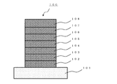
- FIG. 1 is a schematic cross-sectional view showing an organic electroluminescent element according to this embodiment.
- An organic electroluminescent device 100 shown in FIG. 1 includes a substrate 101, an anode 102 provided on the substrate 101, a hole injection layer 103 provided on the anode 102, and a hole injection layer 103.
- the cathode 108 provided on the electron injection layer 107.
- the organic electroluminescent element 100 is manufactured in the reverse order, for example, the substrate 101, the cathode 108 provided on the substrate 101, the electron injection layer 107 provided on the cathode 108, and the electron injection layer.
- a structure including the hole injection layer 103 provided above and the anode 102 provided on the hole injection layer 103 may be employed.
- each said layer may consist of a single layer, respectively, and may consist of multiple layers.
- the substrate 101 serves as a support for the organic electroluminescent device 100, and usually quartz, glass, metal, plastic, or the like is used.
- the substrate 101 is formed into a plate shape, a film shape, or a sheet shape according to the purpose.
- a glass plate, a metal plate, a metal foil, a plastic film, a plastic sheet, or the like is used.
- glass plates and transparent synthetic resin plates such as polyester, polymethacrylate, polycarbonate, polysulfone and the like are preferable.
- soda lime glass, non-alkali glass, or the like is used, and the thickness only needs to be sufficient to maintain the mechanical strength.
- the upper limit value of the thickness is, for example, 2 mm or less, preferably 1 mm or less.
- the glass material is preferably alkali-free glass because it is better to have less ions eluted from the glass.
- soda lime glass with a barrier coat such as SiO 2 is also commercially available, so it can be used. it can.
- the substrate 101 may be provided with a gas barrier film such as a dense silicon oxide film on at least one surface in order to improve the gas barrier property, and a synthetic resin plate, film or sheet having a low gas barrier property is used as the substrate 101. When used, it is preferable to provide a gas barrier film.
- the anode 102 serves to inject holes into the light emitting layer 105.
- the hole injection layer 103 and / or the hole transport layer 104 are provided between the anode 102 and the light emitting layer 105, holes are injected into the light emitting layer 105 through these layers. .
- Examples of the material for forming the anode 102 include inorganic compounds and organic compounds.
- Examples of inorganic compounds include metals (aluminum, gold, silver, nickel, palladium, chromium, etc.), metal oxides (indium oxide, tin oxide, indium-tin oxide (ITO), indium-zinc oxide) Products (IZO), metal halides (copper iodide, etc.), copper sulfide, carbon black, ITO glass, Nesa glass, and the like.
- Examples of the organic compound include polythiophene such as poly (3-methylthiophene), conductive polymer such as polypyrrole and polyaniline, and the like. In addition, it can select suitably from the substances currently used as an anode of an organic electroluminescent element, and can use it.
- the resistance of the transparent electrode is not limited as long as it can supply a sufficient current for light emission of the light emitting element, but is preferably low resistance from the viewpoint of power consumption of the light emitting element.
- an ITO substrate of 300 ⁇ / ⁇ or less functions as an element electrode, but at present, since it is possible to supply a substrate of about 10 ⁇ / ⁇ , for example, 100 to 5 ⁇ / ⁇ , preferably 50 to 5 ⁇ . It is particularly desirable to use low resistance products of / ⁇ .
- the thickness of ITO can be arbitrarily selected according to the resistance value, but is usually used in a range of 50 to 300 nm.
- the hole injection layer 103 plays a role of efficiently injecting holes moving from the anode 102 into the light emitting layer 105 or the hole transport layer 104.
- the hole transport layer 104 plays a role of efficiently transporting holes injected from the anode 102 or holes injected from the anode 102 through the hole injection layer 103 to the light emitting layer 105.
- the hole injection layer 103 and the hole transport layer 104 are each formed by laminating and mixing one kind or two or more kinds of hole injection / transport materials or a mixture of the hole injection / transport material and the polymer binder. Is done.
- an inorganic salt such as iron (III) chloride may be added to the hole injection / transport material to form a layer.
- a hole injection / transport material As a hole injection / transport material, it is necessary to efficiently inject and transport holes from the positive electrode between electrodes to which an electric field is applied. The hole injection efficiency is high, and the injected holes are transported efficiently. It is desirable to do. For this purpose, it is preferable to use a substance that has a low ionization potential, a high hole mobility, excellent stability, and is less likely to generate trapping impurities during production and use.
- a compound conventionally used as a charge transport material for holes, a p-type semiconductor, and a hole injection of an organic electroluminescent element are used.
- Any known material used for the layer and the hole transport layer can be selected and used. Specific examples thereof include carbazole derivatives (N-phenylcarbazole, polyvinylcarbazole, etc.), biscarbazole derivatives such as bis (N-arylcarbazole) or bis (N-alkylcarbazole), triarylamine derivatives (aromatic tertiary class).
- polycarbonate having the above monomers in the side chain And styrene derivatives, polyvinyl carbazole, and polysilane are preferable, but the compound is not particularly limited as long as it is a compound that can form a thin film necessary for manufacturing a light-emitting element, inject holes from the anode, and further transport holes. Absent.
- organic semiconductors are strongly influenced by the doping.
- Such an organic semiconductor matrix material is composed of a compound having a good electron donating property or a compound having a good electron accepting property.
- Strong electron acceptors such as tetracyanoquinone dimethane (TCNQ) or 2,3,5,6-tetrafluorotetracyano-1,4-benzoquinone dimethane (F4TCNQ) are known for doping of electron donor materials.
- TCNQ tetracyanoquinone dimethane
- F4TCNQ 2,3,5,6-tetrafluorotetracyano-1,4-benzoquinone dimethane
- the light emitting layer 105 emits light by recombining holes injected from the anode 102 and electrons injected from the cathode 108 between electrodes to which an electric field is applied.
- the material for forming the light-emitting layer 105 may be a compound that emits light by being excited by recombination of holes and electrons (a light-emitting compound), can form a stable thin film shape, and is in a solid state It is preferable that the compound exhibits a strong light emission (fluorescence) efficiency.
- the compound represented by the above formula (1) can be used as the material for the light emitting layer.
- the light emitting layer may be either a single layer or a plurality of layers, each formed of a light emitting layer material (host material, dopant material).
- a light emitting layer material host material, dopant material
- Each of the host material and the dopant material may be one kind or a plurality of combinations.
- the dopant material may be included in the host material as a whole, or may be included partially.
- As a doping method it can be formed by a co-evaporation method with a host material, but it may be pre-mixed with the host material and then simultaneously deposited.
- the amount of host material used depends on the type of host material and can be determined according to the characteristics of the host material.
- the standard of the amount of the host material used is preferably 50 to 99.999% by weight of the entire light emitting layer material, more preferably 80 to 99.95% by weight, and still more preferably 90 to 99.9% by weight. It is.
- the compound represented by the above formula (1) according to the present invention is particularly preferably a host material.
- the amount of dopant material used depends on the type of dopant material, and can be determined according to the characteristics of the dopant material.
- the standard of the amount of dopant used is preferably 0.001 to 50% by weight, more preferably 0.05 to 20% by weight, and further preferably 0.1 to 10% by weight of the entire material for the light emitting layer. is there.
- the above range is preferable in that, for example, the concentration quenching phenomenon can be prevented.
- Host materials that can be used in combination with the compound represented by the above formula (1) according to the present invention include fused ring derivatives such as anthracene and pyrene, bisstyrylanthracene derivatives and distyryl, which have been known as light emitters.
- fused ring derivatives such as anthracene and pyrene
- bisstyrylanthracene derivatives such as bisstyryl derivatives
- distyryl derivatives such as benzene derivatives, tetraphenylbutadiene derivatives, cyclopentadiene derivatives, fluorene derivatives, and benzofluorene derivatives.
- the dopant material is not particularly limited, and a known compound can be used, and can be selected from various materials according to a desired emission color.
- condensed ring derivatives such as phenanthrene, anthracene, pyrene, tetracene, pentacene, perylene, naphthopylene, dibenzopyrene, rubrene and chrysene, benzoxazole derivatives, benzthiazole derivatives, benzimidazole derivatives, benztriazole derivatives, oxazoles Derivatives, oxadiazole derivatives, thiazole derivatives, imidazole derivatives, thiadiazole derivatives, triazole derivatives, pyrazoline derivatives, stilbene derivatives, thiophene derivatives, tetraphenylbutadiene derivatives, cyclopentadiene derivatives, bisstyrylanthracene derivatives, distyrylbenzene derivative
- blue to blue-green dopant materials include naphthalene, anthracene, phenanthrene, pyrene, triphenylene, perylene, fluorene, indene, chrysene and other aromatic hydrocarbon compounds and derivatives thereof, furan, pyrrole, thiophene, Aromatic complex such as silole, 9-silafluorene, 9,9'-spirobisilafluorene, benzothiophene, benzofuran, indole, dibenzothiophene, dibenzofuran, imidazopyridine, phenanthroline, pyrazine, naphthyridine, quinoxaline, pyrrolopyridine, thioxanthene Ring compounds and their derivatives, distyrylbenzene derivatives, tetraphenylbutadiene derivatives, stilbene derivatives, aldazine derivatives, coumarin derivatives, imidazo
- green to yellow dopant material examples include coumarin derivatives, phthalimide derivatives, naphthalimide derivatives, perinone derivatives, pyrrolopyrrole derivatives, cyclopentadiene derivatives, acridone derivatives, quinacridone derivatives, and naphthacene derivatives such as rubrene.
- a compound in which a substituent capable of increasing the wavelength such as an aryl group, heteroaryl group, arylvinyl group, amino group, cyano group is introduced into the compound exemplified as a blue-green dopant material is also a suitable example.
- orange to red dopant materials include naphthalimide derivatives such as bis (diisopropylphenyl) perylenetetracarboxylic imide, perinone derivatives, rare earth complexes such as Eu complexes having acetylacetone, benzoylacetone and phenanthroline as ligands, 4 -(Dicyanomethylene) -2-methyl-6- (p-dimethylaminostyryl) -4H-pyran and its analogs, metal phthalocyanine derivatives such as magnesium phthalocyanine and aluminum chlorophthalocyanine, rhodamine compounds, deazaflavin derivatives, coumarin derivatives, quinacridone Derivatives, phenoxazine derivatives, oxazine derivatives, quinazoline derivatives, pyrrolopyridine derivatives, squarylium derivatives, violanthrone derivatives, phenazine derivatives, phenoxazo Derivatives and thi
- the dopant can be appropriately selected from the compounds described in Chemical Industry, June 2004, page 13, and references cited therein.
- amines having a stilbene structure perylene derivatives, borane derivatives, aromatic amine derivatives, coumarin derivatives, pyran derivatives or pyrene derivatives are particularly preferable.
- the amine having a stilbene structure is represented by the following formula, for example.
- Ar 1 is an m-valent group derived from aryl having 6 to 30 carbon atoms
- Ar 2 and Ar 3 are each independently aryl having 6 to 30 carbon atoms
- Ar 1 to Ar At least one of 3 has a stilbene structure
- Ar 1 to Ar 3 may be substituted
- m is an integer of 1 to 4.
- the amine having a stilbene structure is more preferably a diaminostilbene represented by the following formula.
- Ar 2 and Ar 3 are each independently aryl having 6 to 30 carbon atoms, and Ar 2 and Ar 3 may be substituted.
- aryl having 6 to 30 carbon atoms include benzene, naphthalene, acenaphthylene, fluorene, phenalene, phenanthrene, anthracene, fluoranthene, triphenylene, pyrene, chrysene, naphthacene, perylene, stilbene, distyrylbenzene, distyrylbiphenyl, and distyryl.
- fluorene include fluorene.
- amines having a stilbene structure include N, N, N ′, N′-tetra (4-biphenylyl) -4,4′-diaminostilbene, N, N, N ′, N′-tetra (1-naphthyl) ) -4,4′-diaminostilbene, N, N, N ′, N′-tetra (2-naphthyl) -4,4′-diaminostilbene, N, N′-di (2-naphthyl) -N, N '-Diphenyl-4,4'-diaminostilbene, N, N'-di (9-phenanthryl) -N, N'-diphenyl-4,4'-diaminostilbene, 4,4'-bis [4 "-bis (Diphenylamino) styryl] -biphenyl, 1,4-bis [4′-bis (diphenylamino)
- perylene derivatives examples include 3,10-bis (2,6-dimethylphenyl) perylene, 3,10-bis (2,4,6-trimethylphenyl) perylene, 3,10-diphenylperylene, 3,4- Diphenylperylene, 2,5,8,11-tetra-t-butylperylene, 3,4,9,10-tetraphenylperylene, 3- (1'-pyrenyl) -8,11-di (t-butyl) perylene 3- (9′-anthryl) -8,11-di (t-butyl) perylene, 3,3′-bis (8,11-di (t-butyl) perylenyl), and the like.
- JP-A-11-97178, JP-A-2000-133457, JP-A-2000-26324, JP-A-2001-267079, JP-A-2001-267078, JP-A-2001-267076, Perylene derivatives described in JP-A No. 2000-34234, JP-A No. 2001-267075, JP-A No. 2001-217077 and the like may be used.
- borane derivatives examples include 1,8-diphenyl-10- (dimesitylboryl) anthracene, 9-phenyl-10- (dimesitylboryl) anthracene, 4- (9′-anthryl) dimesitylborylnaphthalene, 4- (10 ′ -Phenyl-9'-anthryl) dimesitylborylnaphthalene, 9- (dimesitylboryl) anthracene, 9- (4'-biphenylyl) -10- (dimesitylboryl) anthracene, 9- (4 '-(N-carbazolyl) phenyl) And -10- (dimesitylboryl) anthracene.
- the aromatic amine derivative is represented by the following formula, for example.
- Ar 4 is an n-valent group derived from aryl having 6 to 30 carbon atoms
- Ar 5 and Ar 6 are each independently aryl having 6 to 30 carbon atoms
- Ar 4 to Ar 6 are It may be substituted and n is an integer from 1 to 4.
- Ar 4 is a divalent group derived from anthracene, chrysene or pyrene, Ar 5 and Ar 6 are each independently aryl having 6 to 30 carbon atoms, and Ar 4 to Ar 6 are substituted
- An aromatic amine derivative in which n is 2 and n is 2 is more preferable.
- aryl having 6 to 30 carbon atoms include benzene, naphthalene, acenaphthylene, fluorenephenalene, phenanthrene, anthracene, fluoranthene, triphenylene, pyrene, chrysene, naphthacene, perylene, pentacene and the like.
- the chrysene type includes, for example, N, N, N ′, N′-tetraphenylchrysene-6,12-diamine, N, N, N ′, N′-tetra (p-tolyl) Chrysene-6,12-diamine, N, N, N ′, N′-tetra (m-tolyl) chrysene-6,12-diamine, N, N, N ′, N′-tetrakis (4-isopropylphenyl) chrysene -6,12-diamine, N, N, N ', N'-tetra (naphthalen-2-yl) chrysene-6,12-diamine, N, N'-diphenyl-N, N'-di (p-tolyl) ) Chrysene-6,12-diamine, N, N′-diphenyl-N, N′-bis (4
- Examples of the pyrene series include N, N, N ′, N′-tetraphenylpyrene-1,6-diamine, N, N, N ′, N′-tetra (p-tolyl) pyrene-1,6.
- anthracene system examples include N, N, N, N-tetraphenylanthracene-9,10-diamine, N, N, N ′, N′-tetra (p-tolyl) anthracene-9,10-diamine.
- Examples of the pyrene series include N, N, N, N-tetraphenyl-1,8-pyrene-1,6-diamine, N-biphenyl-4-yl-N-biphenyl-1,8-pyrene-1 , 6-diamine, N 1 , N 6 -diphenyl-N 1 , N 6 -bis- (4-trimethylsilanyl-phenyl) -1H, 8H-pyrene-1,6-diamine, and the like.
- Examples of coumarin derivatives include coumarin-6 and coumarin-334. Moreover, you may use the coumarin derivative described in Unexamined-Japanese-Patent No. 2004-43646, Unexamined-Japanese-Patent No. 2001-76876, and Unexamined-Japanese-Patent No. 6-298758.
- Examples of the pyran derivative include the following DCM and DCJTB. Also, JP 2005-126399, JP 2005-097283, JP 2002-234892, JP 2001-220577, JP 2001-081090, and JP 2001-052869. Alternatively, pyran derivatives described in the above may be used.
- the electron injection layer 107 plays a role of efficiently injecting electrons moving from the cathode 108 into the light emitting layer 105 or the electron transport layer 106.
- the electron transport layer 106 plays a role of efficiently transporting electrons injected from the cathode 108 or electrons injected from the cathode 108 through the electron injection layer 107 to the light emitting layer 105.
- the electron transport layer 106 and the electron injection layer 107 are each formed by laminating and mixing one or more electron transport / injection materials or a mixture of the electron transport / injection material and the polymer binder.
- the electron injection / transport layer is a layer that is responsible for injecting electrons from the cathode and further transporting the electrons. It is desirable that the electron injection efficiency is high and the injected electrons are transported efficiently. For this purpose, it is preferable to use a substance that has a high electron affinity, a high electron mobility, excellent stability, and is unlikely to generate trapping impurities during production and use. However, considering the transport balance between holes and electrons, if the role of effectively preventing the holes from the anode from flowing to the cathode side without recombination is mainly played, the electron transport capability is much higher. Even if it is not high, the effect of improving the luminous efficiency is equivalent to that of a material having a high electron transport capability. Therefore, the electron injection / transport layer in this embodiment may include a function of a layer that can efficiently block the movement of holes.
- an electron transport material for forming the electron transport layer 106 or the electron injection layer 107
- a compound conventionally used as an electron transport compound in a photoconductive material an electron injection layer and an electron transport layer of an organic electroluminescent element can be used. It can be arbitrarily selected from known compounds used.
- Materials used for the electron transport layer or the electron injection layer include compounds composed of aromatic rings or heteroaromatic rings composed of one or more atoms selected from carbon, hydrogen, oxygen, sulfur, silicon, and phosphorus, and pyrrole derivatives. And at least one selected from the condensed ring derivatives thereof and metal complexes having electron-accepting nitrogen.
- condensed ring aromatic ring derivatives such as naphthalene and anthracene, styryl aromatic ring derivatives represented by 4,4′-bis (diphenylethenyl) biphenyl, perinone derivatives, coumarin derivatives, naphthalimide derivatives, anthraquinones And quinone derivatives such as diphenoquinone, phosphorus oxide derivatives, carbazole derivatives, and indole derivatives.
- metal complexes having electron-accepting nitrogen include hydroxyazole complexes such as hydroxyphenyloxazole complexes, azomethine complexes, tropolone metal complexes, flavonol metal complexes, and benzoquinoline metal complexes. These materials can be used alone or in combination with different materials.
- electron transfer compounds include pyridine derivatives, naphthalene derivatives, anthracene derivatives, phenanthroline derivatives, perinone derivatives, coumarin derivatives, naphthalimide derivatives, anthraquinone derivatives, diphenoquinone derivatives, diphenylquinone derivatives, perylene derivatives, oxadiazoles.
- metal complexes having electron-accepting nitrogen can also be used, such as hydroxyazole complexes such as quinolinol-based metal complexes and hydroxyphenyloxazole complexes, azomethine complexes, tropolone metal complexes, flavonol metal complexes, and benzoquinoline metal complexes. can give.
- the above-mentioned materials can be used alone, but they may be mixed with different materials.
- quinolinol metal complexes Among the materials described above, quinolinol metal complexes, bipyridine derivatives, phenanthroline derivatives or borane derivatives are preferred.
- the quinolinol-based metal complex is a compound represented by the following general formula (E-1).
- R 1 to R 6 are hydrogen or a substituent
- M is Li, Al, Ga, Be or Zn
- n is an integer of 1 to 3.
- quinolinol metal complexes include 8-quinolinol lithium, tris (8-quinolinolato) aluminum, tris (4-methyl-8-quinolinolato) aluminum, tris (5-methyl-8-quinolinolato) aluminum, tris (3 , 4-dimethyl-8-quinolinolato) aluminum, tris (4,5-dimethyl-8-quinolinolato) aluminum, tris (4,6-dimethyl-8-quinolinolato) aluminum, bis (2-methyl-8-quinolinolato) ( Phenolate) aluminum, bis (2-methyl-8-quinolinolato) (2-methylphenolate) aluminum, bis (2-methyl-8-quinolinolato) (3-methylphenolato) aluminum, bis (2-methyl-8- Quinolinolato) (4- Tylphenolate) aluminum, bis (2-methyl-8-quinolinolato) (2-phenylphenolate) aluminum, bis (2-methyl-8-quinolinolato) (3-phenylphenolate)
- the bipyridine derivative is a compound represented by the following general formula (E-2).
- G represents a simple bond or an n-valent linking group, and n is an integer of 2 to 8. Carbon atoms that are not used for the bond of pyridine-pyridine or pyridine-G may be substituted.
- G in the general formula (E-2) examples include the following structural formulas.
- each R is independently hydrogen, methyl, ethyl, isopropyl, cyclohexyl, phenyl, 1-naphthyl, 2-naphthyl, biphenylyl or terphenylyl.
- pyridine derivative examples include 2,5-bis (2,2′-bipyridin-6-yl) -1,1-dimethyl-3,4-diphenylsilole, 2,5-bis (2,2′- Bipyridin-6-yl) -1,1-dimethyl-3,4-dimesitylsilole, 2,5-bis (2,2′-bipyridin-5-yl) -1,1-dimethyl-3,4 Diphenylsilole, 2,5-bis (2,2′-bipyridin-5-yl) -1,1-dimethyl-3,4-dimesitylsilole, 9,10-di (2,2′-bipyridine-6) -Yl) anthracene, 9,10-di (2,2′-bipyridin-5-yl) anthracene, 9,10-di (2,3′-bipyridin-6-yl) anthracene, 9,10-di (2,3′
- the phenanthroline derivative is a compound represented by the following general formula (E-3-1) or (E-3-2).
- R 1 to R 8 are hydrogen or a substituent, adjacent groups may be bonded to each other to form a condensed ring, G represents a simple bond or an n-valent linking group, and n represents 2 It is an integer of ⁇ 8.
- Examples of G in the general formula (E-3-2) include the same ones as described in the bipyridine derivative column.
- phenanthroline derivatives include 4,7-diphenyl-1,10-phenanthroline, 2,9-dimethyl-4,7-diphenyl-1,10-phenanthroline, 9,10-di (1,10-phenanthroline- 2-yl) anthracene, 2,6-di (1,10-phenanthroline-5-yl) pyridine, 1,3,5-tri (1,10-phenanthroline-5-yl) benzene, 9,9′-difluor -Bis (1,10-phenanthroline-5-yl), bathocuproin, 1,3-bis (2-phenyl-1,10-phenanthroline-9-yl) benzene and the like.
- a phenanthroline derivative is used for the electron transport layer and the electron injection layer.
- a material excellent in thermal stability and thin film formation is desired, and among the phenanthroline derivatives, the substituent itself has a three-dimensional structure, Those having a three-dimensional structure by steric repulsion with an adjacent substituent or those having a plurality of phenanthroline skeletons linked to each other are preferred.
- a compound containing a conjugated bond, a substituted or unsubstituted aromatic hydrocarbon, or a substituted or unsubstituted aromatic heterocycle in the linking unit is more preferable.
- the borane derivative is a compound represented by the following general formula (E-4), and is disclosed in detail in JP-A-2007-27587.
- each of R 11 and R 12 independently represents a hydrogen atom, an alkyl group, an optionally substituted aryl group, a substituted silyl group, an optionally substituted nitrogen-containing heterocyclic group, or a cyano group.
- R 13 to R 16 are each independently an optionally substituted alkyl group or an optionally substituted aryl group
- X is an optionally substituted arylene group
- Y is an optionally substituted aryl group having 16 or less carbon atoms, a substituted boryl group, or an optionally substituted carbazole group
- n is each independently an integer of 0 to 3 is there.
- the compound represented by -1-4) is preferred. Specific examples include 9- [4- (4-Dimesitylborylnaphthalen-1-yl) phenyl] carbazole, 9- [4- (4-Dimesitylborylnaphthalen-1-yl) naphthalen-1-yl. Carbazole and the like.
- each of R 11 and R 12 independently represents a hydrogen atom, an alkyl group, an optionally substituted aryl group, a substituted silyl group, an optionally substituted nitrogen-containing heterocyclic group, or a cyano group.
- R 13 to R 16 is independently an optionally substituted alkyl group or an optionally substituted aryl group
- R 21 and R 22 are each independently , A hydrogen atom, an alkyl group, an optionally substituted aryl group, a substituted silyl group, an optionally substituted nitrogen-containing heterocyclic group, or a cyano group
- X 1 is a substituted Or an arylene group having 20 or less carbon atoms
- n is each independently an integer of 0 to 3
- m is each independently an integer of 0 to 4.
- R 31 to R 34 are each independently methyl, isopropyl or phenyl
- R 35 and R 36 are each independently hydrogen, methyl, isopropyl or phenyl. It is.
- each of R 11 and R 12 independently represents a hydrogen atom, an alkyl group, an optionally substituted aryl group, a substituted silyl group, an optionally substituted nitrogen-containing heterocyclic group, or a cyano group.
- R 13 to R 16 each independently represents an optionally substituted alkyl group or an optionally substituted aryl group, and X 1 represents an optionally substituted carbon.
- R 31 to R 34 are each independently any of methyl, isopropyl or phenyl
- R 35 and R 36 are each independently any of hydrogen, methyl, isopropyl or phenyl It is.
- each of R 11 and R 12 independently represents a hydrogen atom, an alkyl group, an optionally substituted aryl group, a substituted silyl group, an optionally substituted nitrogen-containing heterocyclic group, or a cyano group.
- Each of R 13 to R 16 independently represents an optionally substituted alkyl group or an optionally substituted aryl group, and X 1 represents an optionally substituted carbon.
- R 31 to R 34 are each independently methyl, isopropyl or phenyl
- R 35 and R 36 are each independently hydrogen, methyl, isopropyl or phenyl. It is.
- the benzimidazole derivative is a compound represented by the following general formula (E-5).
- Ar 1 to Ar 3 are each independently hydrogen or aryl having 6 to 30 carbon atoms which may be substituted.
- a benzimidazole derivative which is anthryl optionally substituted with Ar 1 is preferable.
- aryl having 6 to 30 carbon atoms include phenyl, 1-naphthyl, 2-naphthyl, acenaphthylene-1-yl, acenaphthylene-3-yl, acenaphthylene-4-yl, acenaphthylene-5-yl, and fluorene-1- Yl, fluoren-2-yl, fluoren-3-yl, fluoren-4-yl, fluoren-9-yl, phenalen-1-yl, phenalen-2-yl, 1-phenanthryl, 2-phenanthryl, 3-phenanthryl, 4-phenanthryl, 9-phenanthryl, 1-anthryl, 2-anthryl, 9-anthryl, fluoranthen-1-yl, fluoranthen-2-yl, fluoranthen-3-yl, fluoranthen-7-yl, fluoranthen-8-yl, Triphenylene-1-yl, 2-
- benzimidazole derivative examples include 1-phenyl-2- (4- (10-phenylanthracen-9-yl) phenyl) -1H-benzo [d] imidazole, 2- (4- (10- (naphthalene-2) -Yl) anthracen-9-yl) phenyl) -1-phenyl-1H-benzo [d] imidazole, 2- (3- (10- (naphthalen-2-yl) anthracen-9-yl) phenyl) -1- Phenyl-1H-benzo [d] imidazole, 5- (10- (naphthalen-2-yl) anthracen-9-yl) -1,2-diphenyl-1H-benzo [d] imidazole, 1- (4- (10 -(Naphthalen-2-yl) anthracen-9-yl) phenyl) -2-phenyl-1H-benzo [d] imidazole, 2- (4- (9,10-di (n)-
- the electron transport layer or the electron injection layer may further contain a substance capable of reducing the material forming the electron transport layer or the electron injection layer.
- a substance capable of reducing the material forming the electron transport layer or the electron injection layer various substances can be used as long as they have a certain reducing ability.
- Preferred reducing substances include alkali metals such as Na (work function 2.36 eV), K (2.28 eV), Rb (2.16 eV) or Cs (1.95 eV), and Ca (2. 9eV), Sr (2.0 to 2.5 eV) or Ba (2.52 eV), and alkaline earth metals such as those having a work function of 2.9 eV or less are particularly preferable.
- a more preferable reducing substance is an alkali metal of K, Rb or Cs, more preferably Rb or Cs, and most preferably Cs.
- alkali metals have particularly high reducing ability, and by adding a relatively small amount to the material forming the electron transport layer or the electron injection layer, the luminance of the organic EL element can be improved and the lifetime can be extended.
- a reducing substance having a work function of 2.9 eV or less a combination of two or more alkali metals is also preferable.
- a combination containing Cs such as Cs and Na, Cs and K, Cs and Rb, or A combination of Cs, Na and K is preferred.
- Cs such as Cs and Na, Cs and K, Cs and Rb, or A combination of Cs, Na and K is preferred.
- the cathode 108 serves to inject electrons into the light emitting layer 105 through the electron injection layer 107 and the electron transport layer 106.
- the material for forming the cathode 108 is not particularly limited as long as it is a substance that can efficiently inject electrons into the organic layer, but the same material as that for forming the anode 102 can be used.
- metals such as tin, indium, calcium, aluminum, silver, copper, nickel, chromium, gold, platinum, iron, zinc, lithium, sodium, potassium, cesium and magnesium or alloys thereof (magnesium-silver alloy, magnesium -Indium alloys, aluminum-lithium alloys such as lithium fluoride / aluminum, etc.) are preferred.
- Lithium, sodium, potassium, cesium, calcium, magnesium, or alloys containing these low work function metals are effective for increasing the electron injection efficiency and improving device characteristics.
- metals such as platinum, gold, silver, copper, iron, tin, aluminum and indium, or alloys using these metals, and inorganic materials such as silica, titania and silicon nitride, polyvinyl alcohol, vinyl chloride Lamination of hydrocarbon polymer compounds and the like is a preferred example.
- the method for producing these electrodes is not particularly limited as long as conduction can be achieved, such as resistance heating, electron beam, sputtering, ion plating, and coating.
- the materials used for the hole injection layer, hole transport layer, light emitting layer, electron transport layer and electron injection layer can form each layer alone, but as a polymer binder, polyvinyl chloride, polycarbonate, Polystyrene, poly (N-vinylcarbazole), polymethyl methacrylate, polybutyl methacrylate, polyester, polysulfone, polyphenylene oxide, polybutadiene, hydrocarbon resin, ketone resin, phenoxy resin, polyamide, ethyl cellulose, vinyl acetate resin, ABS resin, polyurethane resin It can also be used by dispersing it in solvent-soluble resins such as phenol resins, xylene resins, petroleum resins, urea resins, melamine resins, unsaturated polyester resins, alkyd resins, epoxy resins, silicone resins, etc. is there.
- solvent-soluble resins such as phenol resins, xylene resins, petroleum resins, urea resins, melamine resins,
- Each layer constituting the organic electroluminescent element is formed by a method such as vapor deposition, resistance heating vapor deposition, electron beam vapor deposition, sputtering, molecular lamination method, printing method, spin coating method or cast method, coating method, etc. It can be formed by using a thin film.
- the film thickness of each layer thus formed is not particularly limited and can be appropriately set according to the properties of the material, but is usually in the range of 2 nm to 5000 nm. The film thickness can usually be measured with a crystal oscillation type film thickness measuring device or the like.
- the vapor deposition conditions vary depending on the type of material, the target crystal structure and association structure of the film, and the like.
- Deposition conditions generally include boat heating temperature of 50 to 400 ° C., vacuum degree of 10 ⁇ 6 to 10 ⁇ 3 Pa, deposition rate of 0.01 to 50 nm / second, substrate temperature of ⁇ 150 to + 300 ° C., film thickness of 2 nm to 5 ⁇ m. It is preferable to set appropriately within the range.
- an organic electric field composed of an anode / hole injection layer / hole transport layer / a light emitting layer composed of a host material and a dopant material / electron transport layer / electron injection layer / cathode.
- a method for manufacturing a light-emitting element will be described.
- a thin film of an anode material is formed on a suitable substrate by vapor deposition or the like to produce an anode, and then a thin film of a hole injection layer and a hole transport layer is formed on the anode.
- a host material and a dopant material are co-evaporated to form a thin film to form a light emitting layer.
- An electron transport layer and an electron injection layer are formed on the light emitting layer, and a thin film made of a cathode material is formed by vapor deposition. By forming it as a cathode, a target organic electroluminescent element can be obtained.
- the order of preparation may be reversed, and the cathode, electron injection layer, electron transport layer, light emitting layer, hole transport layer, hole injection layer, and anode may be fabricated in this order. Is possible.
- the anode When a direct current voltage is applied to the organic electroluminescent device thus obtained, the anode may be applied with a positive polarity and the negative electrode with a negative polarity. Luminescence can be observed from the electrode side (anode or cathode, and both).
- the organic electroluminescence device emits light when a pulse current or an alternating current is applied.
- the alternating current waveform to be applied may be arbitrary.
- the present invention can also be applied to a display device provided with an organic electroluminescent element or a lighting device provided with an organic electroluminescent element.
- a display device or an illuminating device including an organic electroluminescent element can be manufactured by a known method such as connecting the organic electroluminescent element according to the present embodiment and a known driving device, such as direct current driving, pulse driving, or alternating current. It can be driven by appropriately using a known driving method such as driving.
- Examples of the display device include a panel display such as a color flat panel display, and a flexible display such as a flexible color organic electroluminescence (EL) display (for example, JP-A-10-335066 and JP-A-2003-321546). Gazette, JP-A-2004-281086, etc.).
- Examples of the display method of the display include a matrix and / or segment method. Note that the matrix display and the segment display may coexist in the same panel.
- a matrix is a pixel in which pixels for display are arranged two-dimensionally, such as a lattice or mosaic, and displays characters and images with a set of pixels.
- the shape and size of the pixel are determined by the application. For example, a square pixel with a side of 300 ⁇ m or less is usually used for displaying images and characters on a personal computer, monitor, TV, and a pixel with a side of mm order for a large display such as a display panel. become.
- monochrome display pixels of the same color may be arranged. However, in color display, red, green, and blue pixels are displayed side by side. In this case, there are typically a delta type and a stripe type.
- the matrix driving method may be either a line sequential driving method or an active matrix.
- the line-sequential driving has an advantage that the structure is simple.
- the active matrix may be superior in consideration of the operation characteristics, so that it is necessary to properly use it depending on the application.
- a pattern is formed so as to display predetermined information, and a predetermined region is caused to emit light.
- a predetermined region is caused to emit light.
- the time and temperature display in a digital clock or a thermometer the operation state display of an audio device or an electromagnetic cooker, the panel display of an automobile, and the like can be mentioned.
- the illuminating device examples include an illuminating device such as indoor lighting, a backlight of a liquid crystal display device, and the like (for example, JP 2003-257621 A, JP 2003-277741 A, JP 2004-119211 A).
- the backlight is used mainly for the purpose of improving the visibility of a display device that does not emit light, and is used for a liquid crystal display device, a clock, an audio device, an automobile panel, a display panel, a sign, and the like.
- a backlight for liquid crystal display devices especially personal computers for which thinning is an issue, considering that conventional methods are made of fluorescent lamps and light guide plates, it is difficult to reduce the thickness.
- the backlight using the light emitting element according to the embodiment is thin and lightweight.
- THF tetrahydrofuran
- IPA isopropyl alcohol
- the target compound (1-2) had a glass transition temperature (Tg) of 133.4 ° C.
- Tg glass transition temperature
- reaction solution was cooled to room temperature, methanol was added, and the precipitate was collected by suction filtration.
- the obtained solid was washed with water and then with methanol, and further washed with ethyl acetate.
- the obtained crude product is dissolved in toluene, passed through an activated carbon short column to remove the colored components, and recrystallized from chlorobenzene to obtain the target compound 9- (9).
- Naphthalen-1-yl) -10- (7-phenylnaphthalen-2-yl) anthracene (1.2 g) was obtained.
- the scheme is shown in “Reaction 7” below.
- reaction solution was cooled to room temperature, methanol was added, and the precipitate was collected by suction filtration.
- the obtained solid was washed with water and then with methanol, and further washed with ethyl acetate.
- the obtained crude product is dissolved in chlorobenzene, passed through an activated carbon short column to remove colored components, and further recrystallized from chlorobenzene to obtain the target compound of formula (1-34).
- ([2,2′-Binaphthalen] -7-yl) -10- (naphthalen-1-yl) anthracene (1.5 g) was obtained.
- the scheme is shown in “Reaction 8” below.
- reaction solution was cooled to room temperature, methanol was added, and the precipitate was collected by suction filtration.
- the obtained solid was washed with water and then with methanol, and further washed with ethyl acetate.
- the obtained crude product is dissolved in chlorobenzene, passed through an activated carbon short column to remove colored components, and further recrystallized from chlorobenzene to obtain the target compound represented by the formula (1-38).
- (7- (10- (Naphthalen-1-yl) anthracen-9-yl) naphthalen-2-yl) triphenylene (1.9 g) was obtained.
- the scheme is shown in “Reaction 10” below.
- reaction liquid was cooled after completion
- the scheme is shown in “Reaction 14” below.
- reaction solution was cooled to room temperature, water was added, and the precipitate was collected by suction filtration.
- the obtained solid was washed with water and then with methanol, and further washed with ethyl acetate.
- the obtained crude product was purified by silica gel column chromatography (solvent: chlorobenzene), and finally recrystallized from chlorobenzene, whereby 9-([1,1, 1′-biphenyl] -3-yl) -10-([2,2′-binaphthalene] -7-yl) anthracene (0.5 g) was obtained.
- the scheme is shown in “Reaction 16” below.
- reaction liquid was cooled to room temperature after completion
- the solvent was distilled off under reduced pressure, and the resulting crude product was purified by silica gel column chromatography (solvent: toluene), and further purified by activated carbon column chromatography (solvent: toluene) to obtain the target formula (1-162).
- 9-([1,1 ′: 3 ′, 1 ′′ -terphenyl] -5′-yl) -10-([2,2′-binaphthalene] -7-yl) anthracene (1.0 g) was obtained.
- the scheme is shown in “Reaction 17” below.
- reaction solution was cooled to room temperature, water was added, and the precipitate was collected by suction filtration.
- the obtained solid was washed with water and then with methanol and purified by silica gel column chromatography (solvent: toluene).
- 9-([2,2′-binaphthalene] -7-yl) -10- (phenanthrene-9-yl) which is the target compound represented by the formula (1-164) by recrystallization from chlorobenzene Anthracene (0.7 g) was obtained.
- the scheme is shown in “Reaction 18” below.
- reaction liquid was cooled to room temperature after completion
- the solvent was distilled off under reduced pressure, and the resulting solid was purified by silica gel column chromatography (solvent: toluene), and further purified by activated carbon column chromatography (solvent: toluene) to obtain the target formula (1-117).
- 9-([1,1′-biphenyl] -2-yl) -10-([2,2′-binaphthalene] -7-yl)) anthracene (0.5 g) was obtained as the compound represented.
- the scheme is shown in “Reaction 19” below.
- reaction solution was cooled to room temperature, water was added, and the precipitate was collected by suction filtration.
- the obtained solid was washed with water and then with methanol, and then purified by silica gel column chromatography (solvent: toluene), and further purified by activated carbon column chromatography (solvent: toluene) to obtain the target formula (1-129).
- solvent: toluene 9-([1,1′-biphenyl] -4-yl) -10-([2,2′-binaphthalene] -7-yl)) anthracene (0.6 g) was obtained. .
- the scheme is shown in “Reaction 20” below.
- reaction solution was cooled to room temperature, water was added, and the precipitate was collected by suction filtration.
- the obtained solid was washed with water and then methanol, dissolved in chlorobenzene, and passed through activated alumina column chromatography (solvent: toluene).
- the scheme is shown in “Reaction 24” below.
- reaction liquid was cooled to room temperature after completion
- solvent heptane / toluene mixed solvent
- reaction liquid was cooled to room temperature after completion
- the crude product obtained here was washed with ethyl acetate, so that 9-([2,2′-binaphthalene] -7-yl) -10- which was the target compound represented by the formula (1-172) was obtained.
- (4-Phenylnaphthalen-1-yl) anthracene (1.7 g) was obtained.
- the scheme is shown in “Reaction 31” below.
- Example 1 The elements according to Example 1 and Comparative Example 1 were manufactured, and the driving start voltage (V) in a constant current driving test at a current density at which a luminance of 2000 cd / m 2 was obtained, and 80% of the initial luminance (1600 cd / m). 2 ) The time (hr) for maintaining the above luminance was measured.
- V driving start voltage
- hr initial luminance
- Table 1 below shows the material configuration of each layer in the manufactured organic EL elements according to Example 1 and Comparative Example 1.
- HI is N 4 , N 4 ′ -diphenyl-N 4 , N 4 ′ -bis (9-phenyl-9H-carbazol-3-yl)-[1,1′-biphenyl] -4, 4′-diamine
- NPD is N, N′-diphenyl-N, N′-dinaphthyl-4,4′-diaminobiphenyl
- BH1 is 9- (6-([1,1′-biphenyl]- 3-yl) naphthalen-2-yl) -10-phenylanthracene
- BD1 is 7,7, N 5 , N 9 -tetraphenyl-N 5 , N 9 -bis- (4-trimethylsilanyl-phenyl) -7H-benzo [c] fluorene-5,9-diamine
- ET1 is 2- (4- (9,10-di (naphthalen-2-yl) anthracen-2
- Example 1 ⁇ Device using Compound (1-2) as Host Material for Light-Emitting Layer>
- a glass substrate of 26 mm ⁇ 28 mm ⁇ 0.7 mm obtained by polishing ITO deposited to a thickness of 180 nm by sputtering to 150 nm was used as a transparent support substrate.
- the transparent support substrate is fixed to a substrate holder of a commercially available vapor deposition apparatus (manufactured by Showa Vacuum Co., Ltd.), a molybdenum vapor deposition boat containing HI, a molybdenum vapor deposition boat containing NPD, the compound of the present invention (1 -2) Molybdenum vapor deposition boat with BD1, molybdenum vapor deposition boat with BD1, molybdenum vapor deposition boat with ET1, molybdenum vapor deposition boat with Liq, and tungsten vapor deposition with aluminum A boat was installed.
- a commercially available vapor deposition apparatus manufactured by Showa Vacuum Co., Ltd.
- a molybdenum vapor deposition boat containing HI a molybdenum vapor deposition boat containing NPD
- the compound of the present invention (1 -2)
- Molybdenum vapor deposition boat with BD1 molybdenum vapor deposition boat with BD
- the following layers were sequentially formed on the ITO film of the transparent support substrate.
- the vacuum chamber was depressurized to 5 ⁇ 10 ⁇ 4 Pa, first, a vapor deposition boat containing HI was heated and vapor-deposited to a film thickness of 40 nm to form a hole injection layer, and then NPD was contained. The vapor deposition boat was heated and vapor-deposited to a film thickness of 25 nm to form a hole transport layer. Next, the vapor deposition boat containing the compound (1-2) and the vapor deposition boat containing BD1 were heated at the same time to form a light emitting layer by vapor deposition to a film thickness of 25 nm.
- the deposition rate was adjusted so that the weight ratio of compound (1-2) to BD1 was approximately 95: 5.
- the vapor deposition boat containing ET1 and the vapor deposition boat containing Liq were heated at the same time so as to have a film thickness of 25 nm to form an electron transport layer.
- the deposition rate was adjusted so that the weight ratio of ET1 to Liq was approximately 1: 1.
- the deposition rate of each layer was 0.01 to 1 nm / second.
- the evaporation boat containing Liq was heated to deposit at a deposition rate of 0.01 to 0.1 nm / second so as to have a film thickness of 1 nm.
- a vapor deposition boat containing aluminum was heated, and aluminum was deposited at a deposition rate of 0.01 to 2 nm / second so as to have a film thickness of 100 nm to form a cathode, thereby obtaining an organic EL device.
- Example 1 An organic EL device was obtained in the same manner as in Example 1 except that the compound (1-2) as the host material for the light emitting layer was changed to BH1.
- the driving test starting voltage was 4.34 V and 80% of the initial luminance.
- the time for maintaining the luminance of (1600 cd / m 2 ) or more was 455 hours.
- Table 3 below shows the material structure of each layer in the produced organic EL elements according to Examples 2 to 11 and Comparative Examples 2 to 4.
- BD2 is 7,7-dimethyl-N 5 , N 9 -diphenyl-N 5 , N 9 -bis- (4-trimethylsilanyl-phenyl) -7H-benzo [c] fluorene-5 9-diamine
- ET2 is 4,4 ′-((2-phenylanthracene-9,10-diyl) bis (4,1-phenylene)) dipyridine
- BH2 is 9-([2,2′- Binaphthalene] -6-yl) -10-phenylanthracene
- BH3 is 9-phenyl-10- (6-phenylnaphthalen-2-yl) anthracene. The chemical structure is shown below.
- Example 2 ⁇ Device Using Compound (1-1) as Host Material for Light-Emitting Layer> A glass substrate of 26 mm ⁇ 28 mm ⁇ 0.7 mm (manufactured by Optoscience Co., Ltd.) obtained by polishing ITO deposited to a thickness of 180 nm by sputtering to 150 nm was used as a transparent support substrate.
- This transparent support substrate is fixed to a substrate holder of a commercially available vapor deposition apparatus (manufactured by Showa Vacuum Co., Ltd.), a molybdenum vapor deposition boat containing HI, a molybdenum vapor deposition boat containing NPD, compound (1-1) Molybdenum vapor deposition boat with BD2, molybdenum vapor deposition boat with BD2, molybdenum vapor deposition boat with ET2, molybdenum vapor deposition boat with Liq, molybdenum boat with magnesium and silver A tungsten evaporation boat was attached.
- a commercially available vapor deposition apparatus manufactured by Showa Vacuum Co., Ltd.
- the following layers were sequentially formed on the ITO film of the transparent support substrate.
- the vacuum chamber was depressurized to 5 ⁇ 10 ⁇ 4 Pa, first, a vapor deposition boat containing HI was heated and vapor-deposited to a film thickness of 40 nm to form a hole injection layer, and then NPD was contained. The vapor deposition boat was heated and vapor-deposited to a film thickness of 25 nm to form a hole transport layer. Next, the vapor deposition boat containing the compound (1-1) and the vapor deposition boat containing BD2 were heated at the same time to form a light emitting layer by vapor deposition to a film thickness of 25 nm.
- the deposition rate was adjusted so that the weight ratio of compound (1-1) to BD2 was approximately 95: 5.
- the evaporation boat containing ET2 was heated and evaporated to a thickness of 20 nm to form an electron transport layer.
- the deposition rate of each layer was 0.01 to 1 nm / second.
- the evaporation boat containing Liq was heated to deposit at a deposition rate of 0.01 to 0.1 nm / second so as to have a film thickness of 1 nm.
- a boat containing magnesium and a boat containing silver were heated at the same time and evaporated to a film thickness of 100 nm to form a cathode.
- the deposition rate was adjusted so that the atomic ratio of magnesium and silver was 10: 1, and the cathode was formed so that the deposition rate was 0.1 to 10 nm / second, to obtain an organic electroluminescent device.
- Example 3 An organic EL device was obtained in the same manner as in Example 2, except that the compound (1-1) as the host material for the light emitting layer was changed to the compound (1-34).
- the driving test starting voltage was 3.93 V and 80% of the initial luminance.
- the time for maintaining the luminance of (1600 cd / m 2 ) or more was 276 hours.
- Example 4 An organic EL device was obtained by the method according to Example 2 except that the compound (1-1) as the host material for the light emitting layer was changed to the compound (1-21).
- the driving test starting voltage was 4.03 V, which was 80% of the initial luminance.
- the time for maintaining the luminance of (1600 cd / m 2 ) or more was 265 hours.
- Example 5 An organic EL device was obtained by the method according to Example 2 except that the compound (1-1) as the host material for the light emitting layer was changed to the compound (1-38).
- the driving test starting voltage was 3.70 V and 80% of the initial luminance.
- the time for maintaining the luminance of (1600 cd / m 2 ) or more was 235 hours.
- Example 6 An organic EL device was obtained by the method according to Example 2 except that the compound (1-1) as the host material for the light emitting layer was changed to the compound (1-160).
- the driving test starting voltage was 3.98 V and 80% of the initial luminance.
- the time for maintaining the luminance of (1600 cd / m 2 ) or more was 228 hours.
- Example 7 An organic EL device was obtained in the same manner as in Example 2 except that the compound (1-1) as the host material for the light emitting layer was changed to the compound (1-162).
- the driving test starting voltage was 4.15 V, which was 80% of the initial luminance.
- the time for maintaining the luminance of (1600 cd / m 2 ) or more was 263 hours.
- Example 8 An organic EL device was obtained by the method according to Example 2 except that the compound (1-1) as the host material for the light emitting layer was changed to the compound (1-164).
- the driving test starting voltage was 3.67 V and 80% of the initial luminance.
- the time for maintaining the luminance of (1600 cd / m 2 ) or more was 271 hours.
- Example 9 An organic EL device was obtained in the same manner as in Example 2 except that the compound (1-1) as the host material for the light emitting layer was changed to the compound (1-172).
- the driving test starting voltage was 3.82 V and 80% of the initial luminance.
- the time for maintaining the luminance of (1600 cd / m 2 ) or more was 261 hours.
- Example 10 An organic EL device was obtained by the method according to Example 2 except that the compound (1-1) as the host material for the light emitting layer was changed to the compound (1-117).
- the driving test starting voltage was 4.30 V, which was 80% of the initial luminance.
- the time for maintaining the luminance of (1600 cd / m 2 ) or more was 275 hours.
- Example 11 An organic EL device was obtained by the method according to Example 2 except that the compound (1-1) as the host material for the light emitting layer was changed to the compound (1-184).
- the driving test starting voltage was 4.21 V and 80% of the initial luminance.
- the time for maintaining the luminance of (1600 cd / m 2 ) or more was 231 hours.
- Example 2 An organic EL device was obtained in the same manner as in Example 2 except that the compound (1-1) as the host material for the light emitting layer was changed to BH1.
- the driving test starting voltage was 4.78 V, which was 80% of the initial luminance.
- the time for maintaining the luminance of (1600 cd / m 2 ) or more was 178 hours.
- Example 3 An organic EL device was obtained in the same manner as in Example 2 except that the compound (1-1) serving as the host material for the light emitting layer was changed to BH2.
- the driving test starting voltage was 4.35 V, which was 80% of the initial luminance.
- the time for maintaining the luminance of (1600 cd / m 2 ) or more was 189 hours.
- an organic electroluminescent element having excellent luminous efficiency and element lifetime, a display device including the same, a lighting device including the same.
Landscapes
- Chemical & Material Sciences (AREA)
- Organic Chemistry (AREA)
- Engineering & Computer Science (AREA)
- Materials Engineering (AREA)
- Physics & Mathematics (AREA)
- Spectroscopy & Molecular Physics (AREA)
- Optics & Photonics (AREA)
- Electroluminescent Light Sources (AREA)
- Organic Low-Molecular-Weight Compounds And Preparation Thereof (AREA)
Abstract
Description
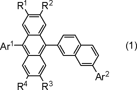
式(1)中、
Ar1は、置換されていてもよい、炭素数10~30のアリールであり、
Ar2は、置換されていてもよい、炭素数6~30のアリールであり、
R1~R4は、それぞれ独立して、水素または炭素数1~4のアルキルであり、そして、
式(1)で表される化合物における少なくとも1つの水素が重水素で置換されていてもよい。
Ar2は、フェニル、ナフチル、ビフェニリル、ビナフチル、テルフェニリル、クアテルフェニリル、ナフチルフェニル、フェニルナフチル、フェナントリル、フェナントリルフェニル、クリセニル、ピレニルフェニルまたはトリフェニレニルであり、これらは炭素数1~12のアルキルまたは炭素数3~12のシクロアルキルで置換されていてもよく、
R1~R4は、それぞれ独立して、水素、メチル、イソプロピルまたはt-ブチルであり、そして、
式(1)で表される化合物における少なくとも1つの水素が重水素で置換されていてもよい、
上記[1]に記載の化合物。
Ar2は、フェニル、1-ナフチル、2-ナフチル、2-ビフェニリル、3-ビフェニリル、4-ビフェニリル、m-テルフェニル-5’-イル、4-(ナフタレン-1-イル)フェニル、4-(ナフタレン-2-イル)フェニル、フェナントレン-9-イルまたはトリフェニレン-2-イルであり、
R1~R4は、水素であり、そして、
式(1)で表される化合物における少なくとも1つの水素が重水素で置換されていてもよい、
上記[1]または[2]に記載の化合物。
Ar2における少なくとも1つの水素が重水素で置換されていてもよい、
上記[3]に記載の化合物。


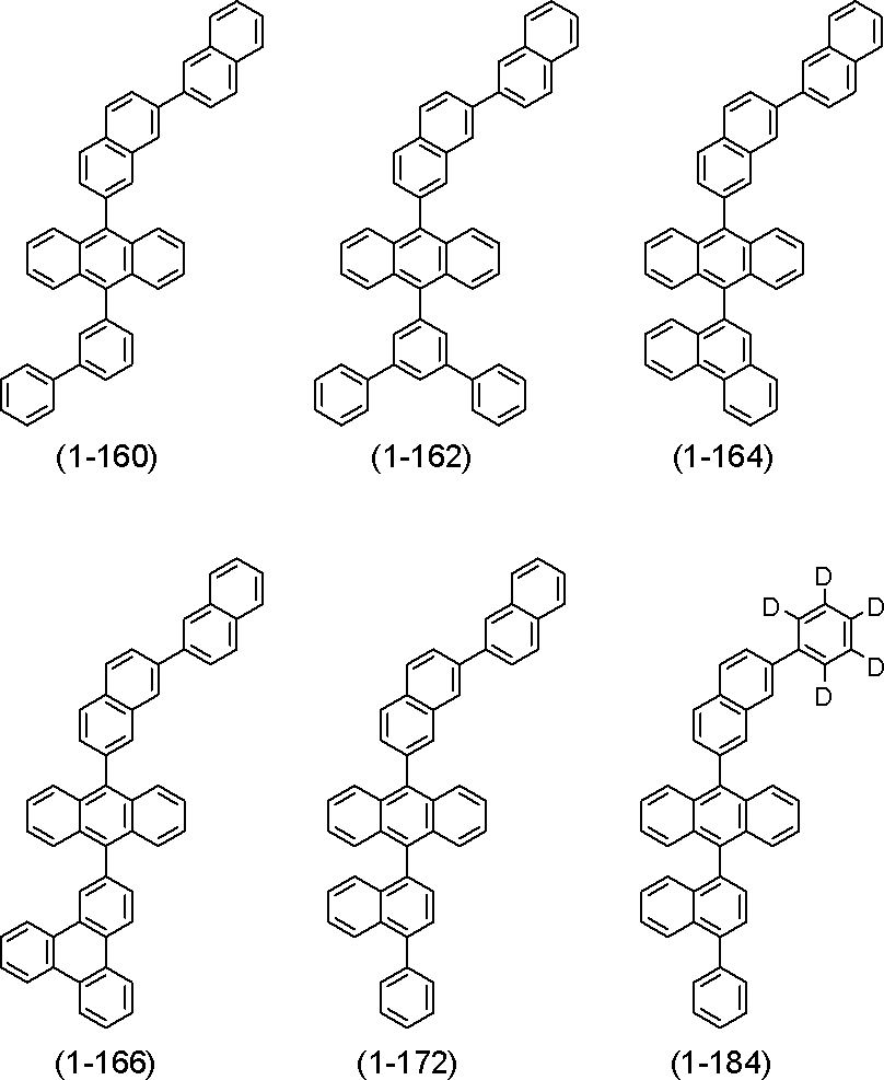
まず、上記一般式(1)で表されるアントラセン化合物について詳細に説明する。本発明の化合物は、9位に炭素数10以上のアリールが結合し、10位にナフチル基が結合したアントラセン化合物において、ナフチル基(その2位においてアントラセンと結合)の特に7位に特定のアリールを置換させた化合物であり、このような置換位置およびアリール構造を選択することで、発光層用材料としてより優れた素子寿命を達成した化合物である。
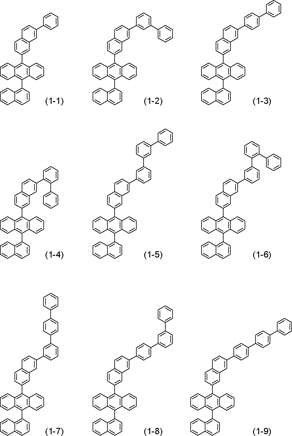

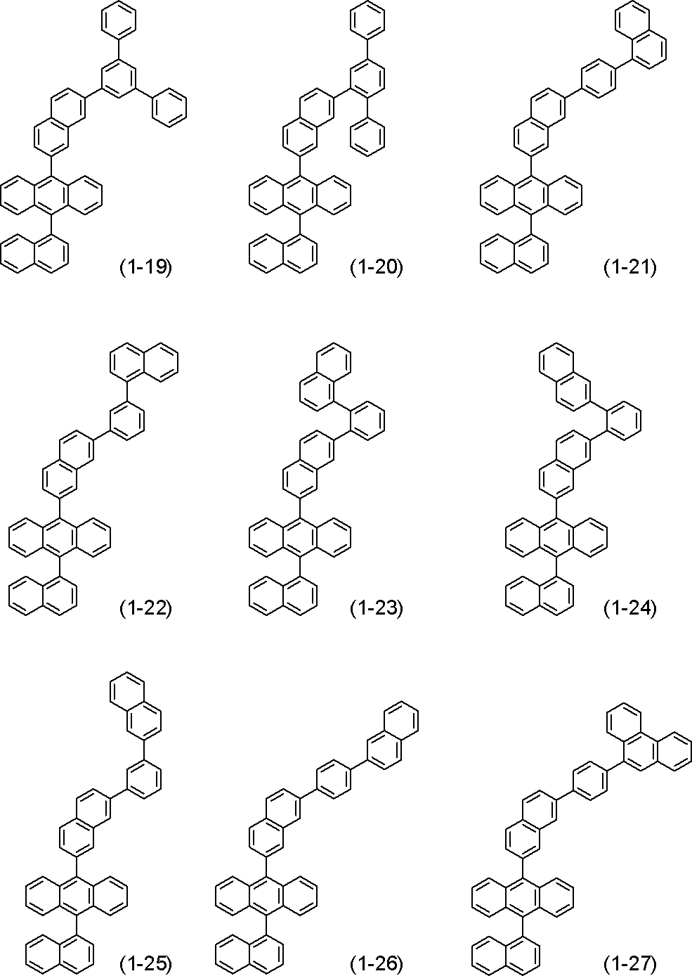
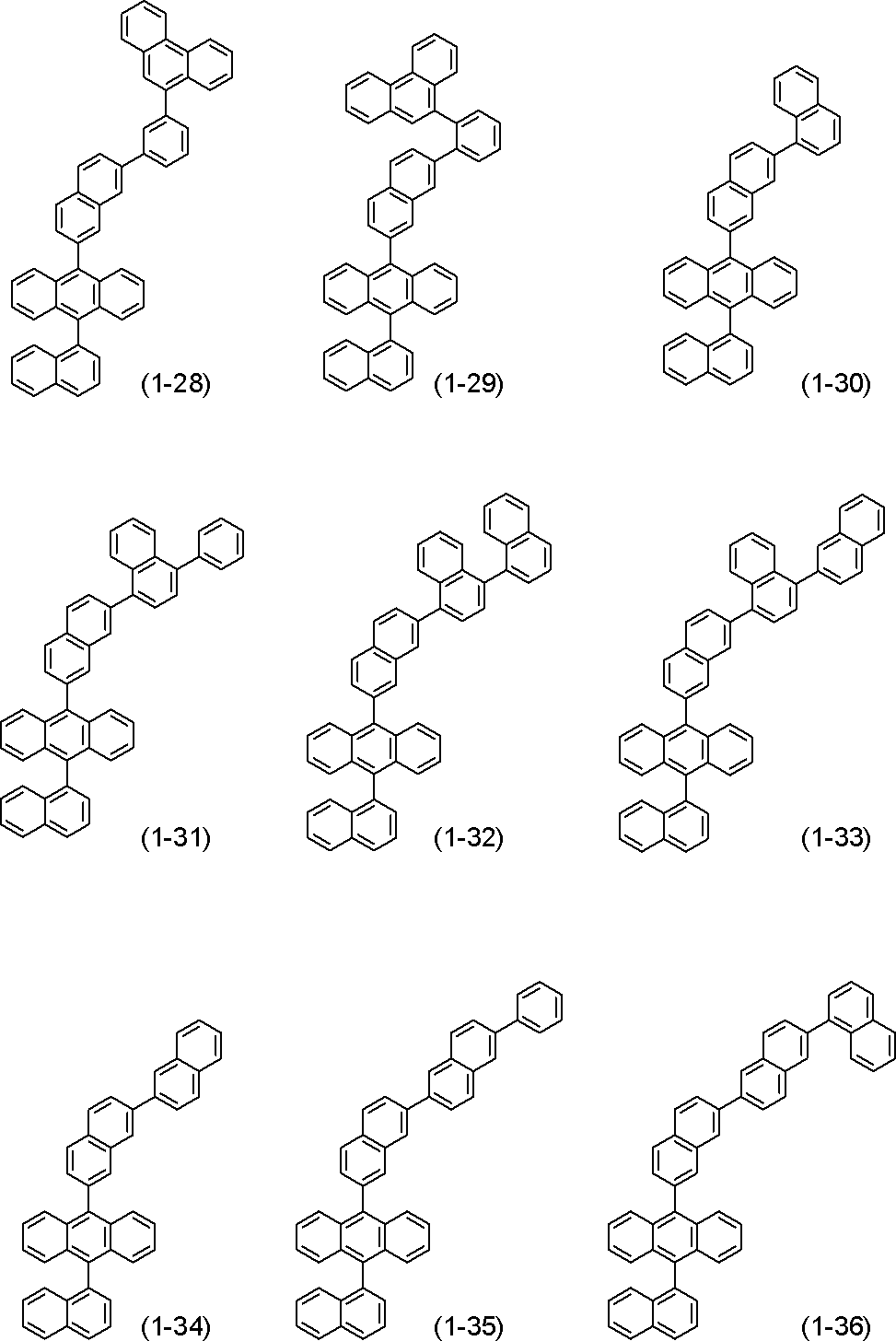

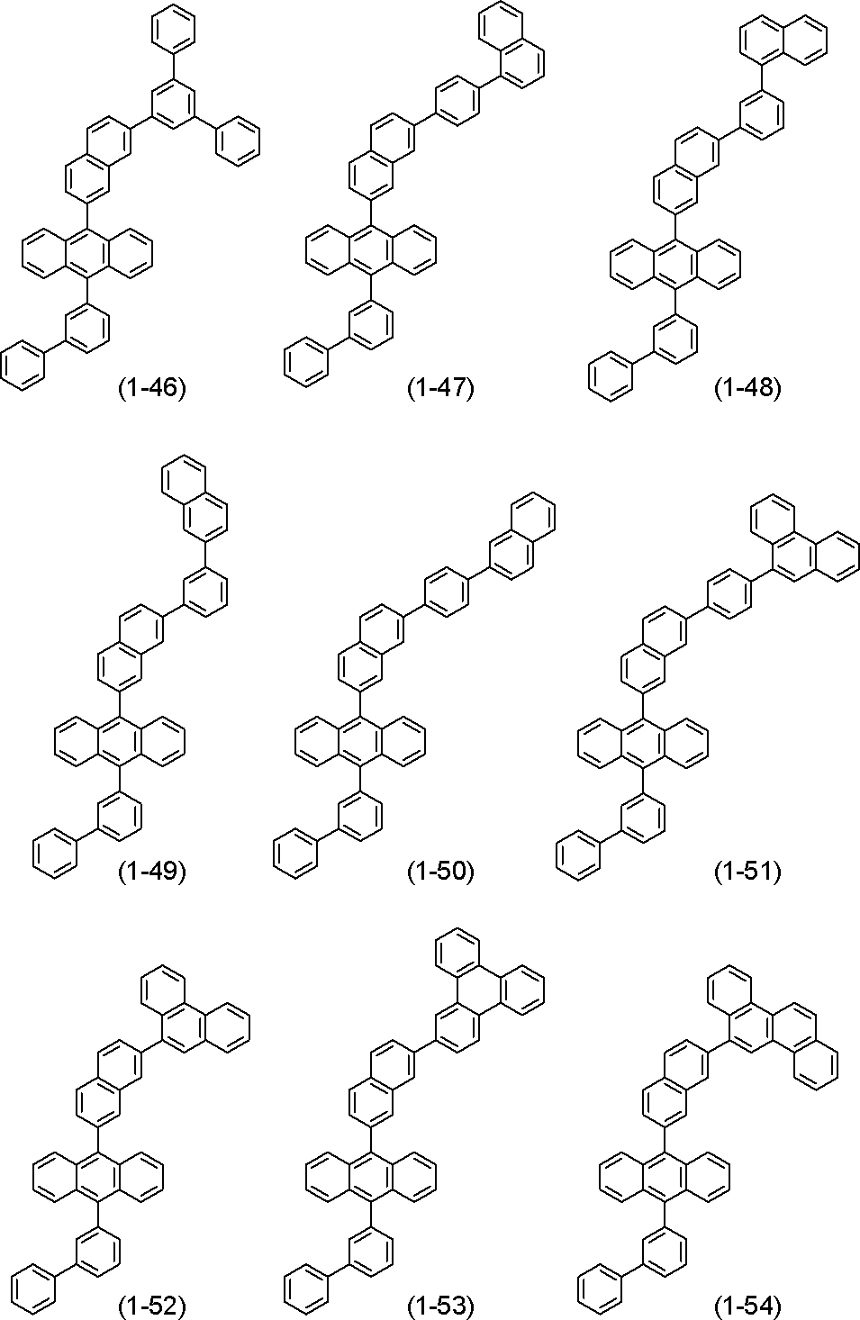

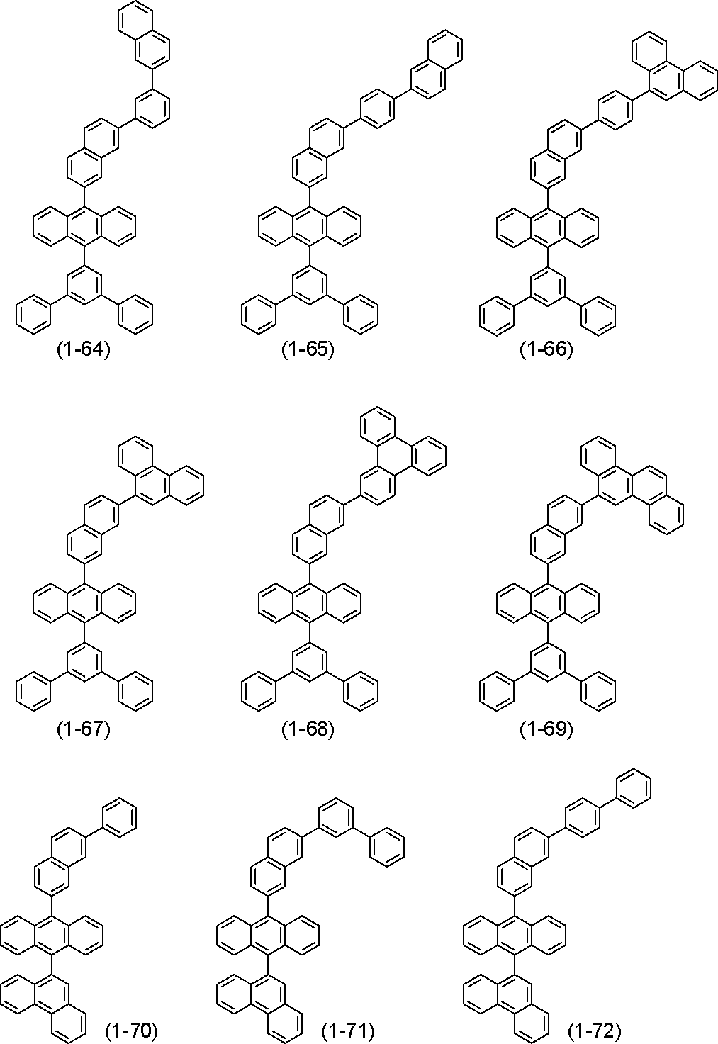
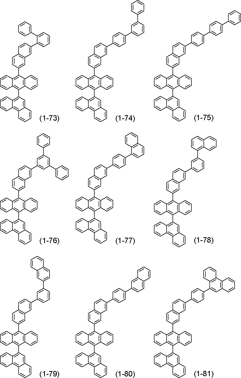
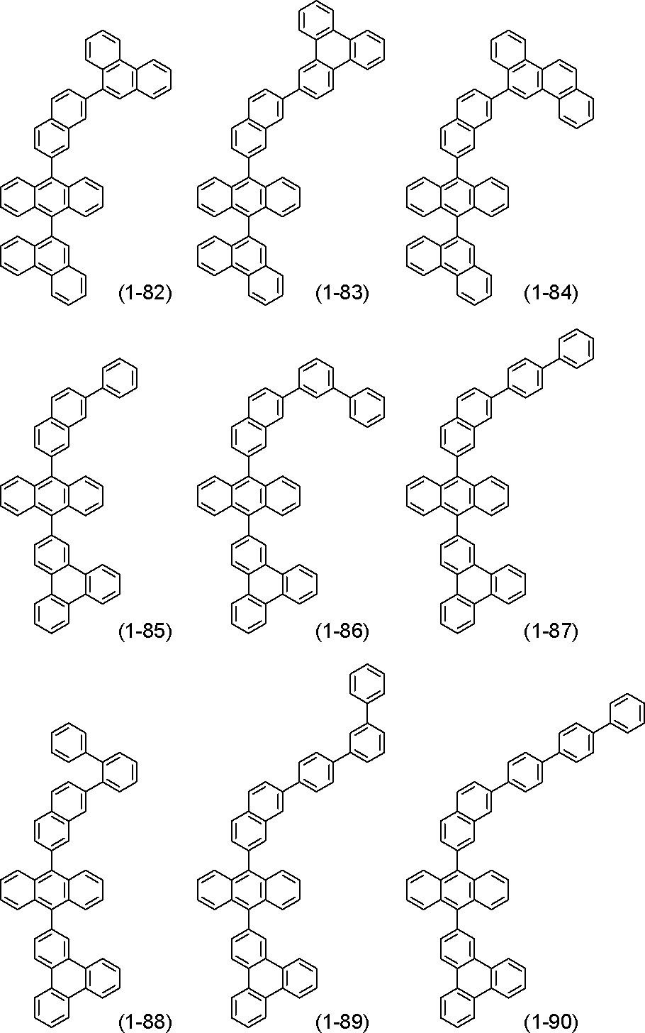

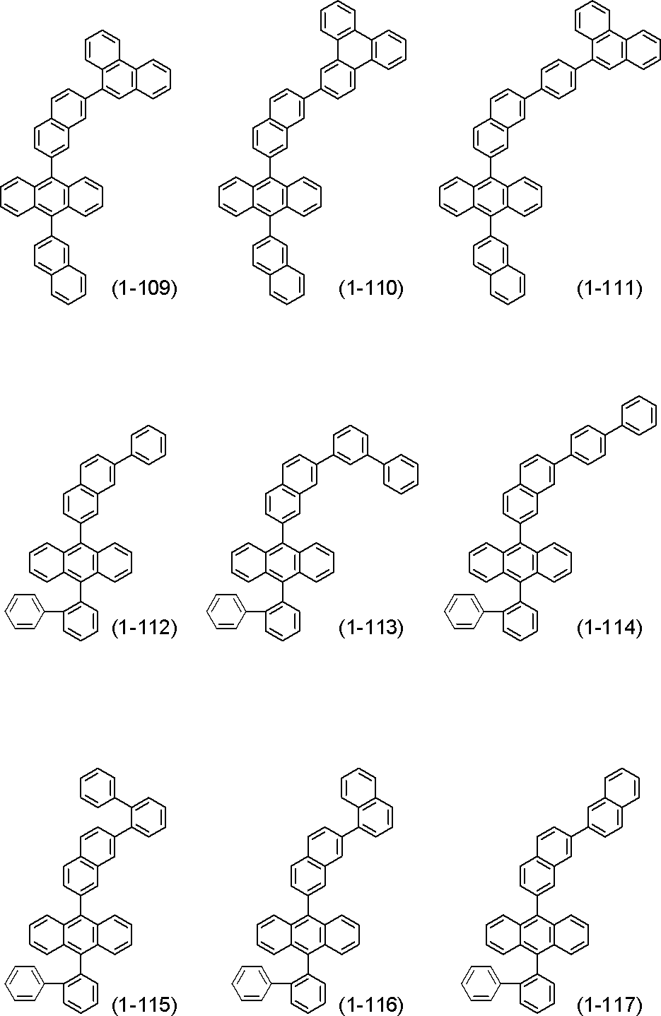


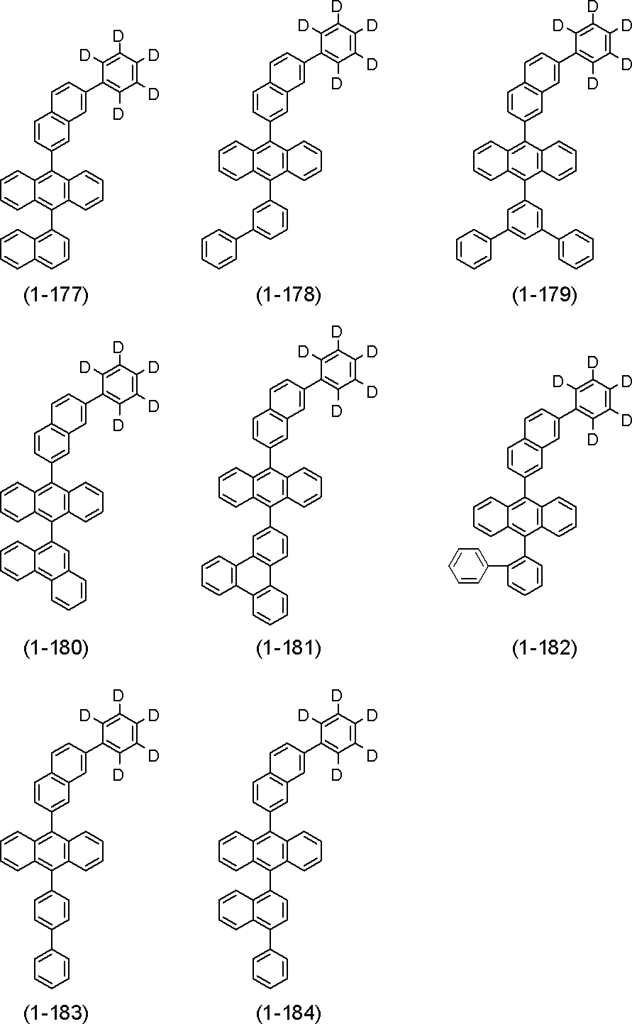
式(1)で表されるアントラセン化合物は、既知の合成法を利用して製造することができる。例えば、下記の反応(A-1)~(A-3)に示す経路にしたがって合成することができる。また、下記の反応(B-1)~(B-5)に示す経路にしたがっても合成することもできる。



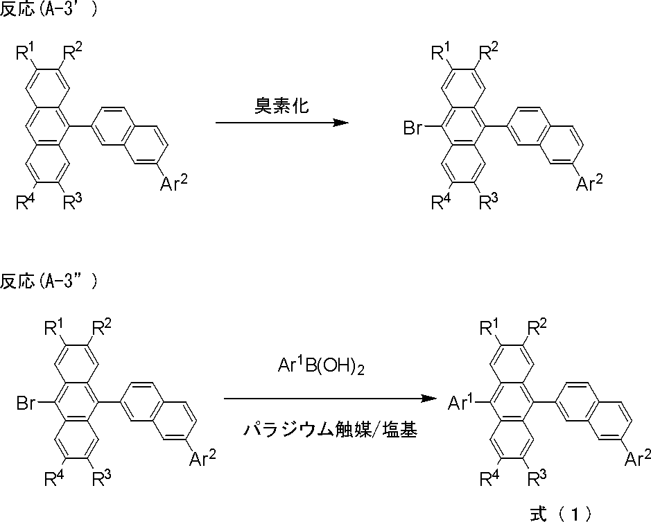
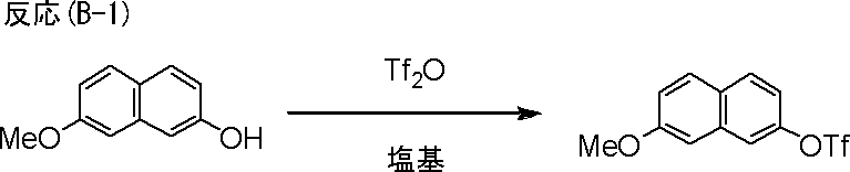
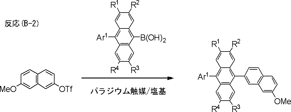
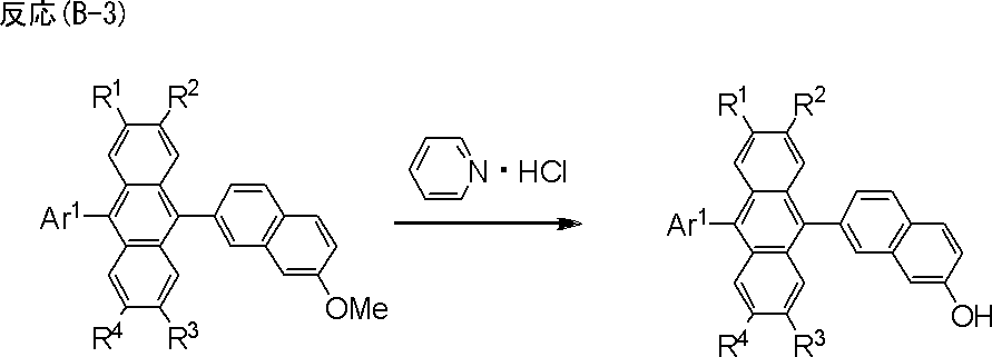
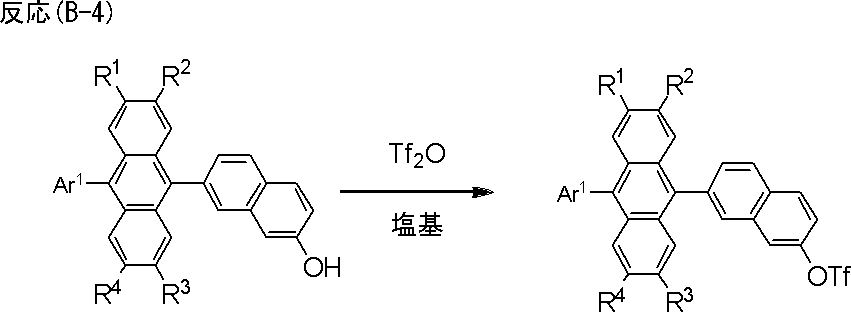

本発明に係るアントラセン化合物は、例えば、有機電界発光素子の材料として用いることができる。以下に、本実施形態に係る有機電界発光素子について図面に基づいて詳細に説明する。図1は、本実施形態に係る有機電界発光素子を示す概略断面図である。
図1に示された有機電界発光素子100は、基板101と、基板101上に設けられた陽極102と、陽極102の上に設けられた正孔注入層103と、正孔注入層103の上に設けられた正孔輸送層104と、正孔輸送層104の上に設けられた発光層105と、発光層105の上に設けられた電子輸送層106と、電子輸送層106の上に設けられた電子注入層107と、電子注入層107の上に設けられた陰極108とを有する。
基板101は、有機電界発光素子100の支持体となるものであり、通常、石英、ガラス、金属、プラスチックなどが用いられる。基板101は、目的に応じて板状、フィルム状、またはシート状に形成され、例えば、ガラス板、金属板、金属箔、プラスチックフィルム、プラスチックシートなどが用いられる。なかでも、ガラス板、および、ポリエステル、ポリメタクリレート、ポリカーボネート、ポリスルホンなどの透明な合成樹脂製の板が好ましい。ガラス基板であれば、ソーダライムガラスや無アルカリガラスなどが用いられ、また、厚みも機械的強度を保つのに十分な厚みがあればよいので、例えば、0.2mm以上あればよい。厚さの上限値としては、例えば、2mm以下、好ましくは1mm以下である。ガラスの材質については、ガラスからの溶出イオンが少ない方がよいので無アルカリガラスの方が好ましいが、SiO2などのバリアコートを施したソーダライムガラスも市販されているのでこれを使用することができる。また、基板101には、ガスバリア性を高めるために、少なくとも片面に緻密なシリコン酸化膜などのガスバリア膜を設けてもよく、特にガスバリア性が低い合成樹脂製の板、フィルムまたはシートを基板101として用いる場合にはガスバリア膜を設けるのが好ましい。
陽極102は、発光層105へ正孔を注入する役割を果たすものである。なお、陽極102と発光層105との間に正孔注入層103および/または正孔輸送層104が設けられている場合には、これらを介して発光層105へ正孔を注入することになる。
正孔注入層103は、陽極102から移動してくる正孔を、効率よく発光層105内または正孔輸送層104内に注入する役割を果たすものである。正孔輸送層104は、陽極102から注入された正孔または陽極102から正孔注入層103を介して注入された正孔を、効率よく発光層105に輸送する役割を果たすものである。正孔注入層103および正孔輸送層104は、それぞれ、正孔注入・輸送材料の一種または二種以上を積層、混合するか、正孔注入・輸送材料と高分子結着剤の混合物により形成される。また、正孔注入・輸送材料に塩化鉄(III)のような無機塩を添加して層を形成してもよい。
発光層105は、電界を与えられた電極間において、陽極102から注入された正孔と、陰極108から注入された電子とを再結合させることにより発光するものである。発光層105を形成する材料としては、正孔と電子との再結合によって励起されて発光する化合物(発光性化合物)であればよく、安定な薄膜形状を形成することができ、かつ、固体状態で強い発光(蛍光)効率を示す化合物であるのが好ましい。本発明では、発光層用の材料として、上記式(1)で表される化合物を用いることができる。

当該式中、Ar1は炭素数6~30のアリールに由来するm価の基であり、Ar2およびAr3は、それぞれ独立して炭素数6~30のアリールであるが、Ar1~Ar3の少なくとも1つはスチルベン構造を有し、Ar1~Ar3は置換されていてもよく、そして、mは1~4の整数である。
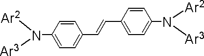
当該式中、Ar2およびAr3は、それぞれ独立して炭素数6~30のアリールであり、Ar2およびAr3は置換されていてもよい。
また、特開2003-347056号公報、および特開2001-307884号公報等に記載されたスチルベン構造を有するアミンを用いてもよい。
また、特開平11-97178号公報、特開2000-133457号公報、特開2000-26324号公報、特開2001-267079号公報、特開2001-267078号公報、特開2001-267076号公報、特開2000-34234号公報、特開2001-267075号公報、および特開2001-217077号公報などに記載されたペリレン誘導体を用いてもよい。
また、国際公開第2000/40586号パンフレットなどに記載されたボラン誘導体を用いてもよい。

当該式中、Ar4は炭素数6~30のアリールに由来するn価の基であり、Ar5およびAr6はそれぞれ独立して炭素数6~30のアリールであり、Ar4~Ar6は置換されていてもよく、そして、nは1~4の整数である。
また、特開2006-156888号公報などに記載された芳香族アミン誘導体を用いてもよい。
また、特開2004-43646号公報、特開2001-76876号公報、および特開平6-298758号公報などに記載されたクマリン誘導体を用いてもよい。

また、特開2005-126399号公報、特開2005-097283号公報、特開2002-234892号公報、特開2001-220577号公報、特開2001-081090号公報、および特開2001-052869号公報などに記載されたピラン誘導体を用いてもよい。
電子注入層107は、陰極108から移動してくる電子を、効率よく発光層105内または電子輸送層106内に注入する役割を果たすものである。電子輸送層106は、陰極108から注入された電子または陰極108から電子注入層107を介して注入された電子を、効率よく発光層105に輸送する役割を果たすものである。電子輸送層106および電子注入層107は、それぞれ、電子輸送・注入材料の一種または二種以上を積層、混合するか、電子輸送・注入材料と高分子結着剤の混合物により形成される。
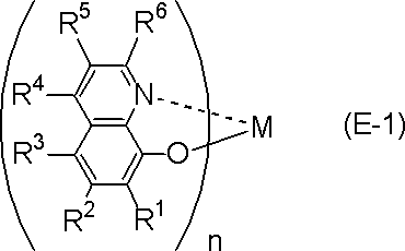
式中、R1~R6は水素または置換基であり、MはLi、Al、Ga、BeまたはZnであり、nは1~3の整数である。
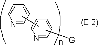
式中、Gは単なる結合手またはn価の連結基を表し、nは2~8の整数である。また、ピリジン-ピリジンまたはピリジン-Gの結合に用いられない炭素原子は置換されていてもよい。
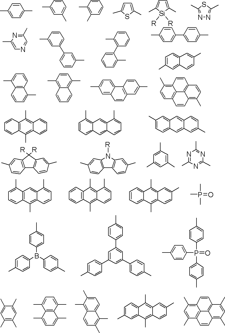

式中、R1~R8は水素または置換基であり、隣接する基は互いに結合して縮合環を形成してもよく、Gは単なる結合手またはn価の連結基を表し、nは2~8の整数である。また、一般式(E-3-2)のGとしては、例えば、ビピリジン誘導体の欄で説明したものと同じものがあげられる。
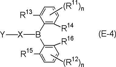
式中、R11およびR12は、それぞれ独立して、水素原子、アルキル基、置換されていてもよいアリール基、置換シリル基、置換されていてもよい窒素含有複素環基、またはシアノ基の少なくとも一つであり、R13~R16は、それぞれ独立して、置換されていてもよいアルキル基、または置換されていてもよいアリール基であり、Xは、置換されていてもよいアリーレン基であり、Yは、置換されていてもよい炭素数16以下のアリール基、置換ボリル基、または置換されていてもよいカルバゾール基であり、そして、nはそれぞれ独立して0~3の整数である。
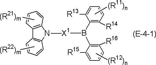
式中、R11およびR12は、それぞれ独立して、水素原子、アルキル基、置換されていてもよいアリール基、置換シリル基、置換されていてもよい窒素含有複素環基、またはシアノ基の少なくとも一つであり、R13~R16は、それぞれ独立して、置換されていてもよいアルキル基、または置換されていてもよいアリール基であり、R21およびR22は、それぞれ独立して、水素原子、アルキル基、置換されていてもよいアリール基、置換シリル基、置換されていてもよい窒素含有複素環基、またはシアノ基の少なくとも一つであり、X1は、置換されていてもよい炭素数20以下のアリーレン基であり、nはそれぞれ独立して0~3の整数であり、そして、mはそれぞれ独立して0~4の整数である。
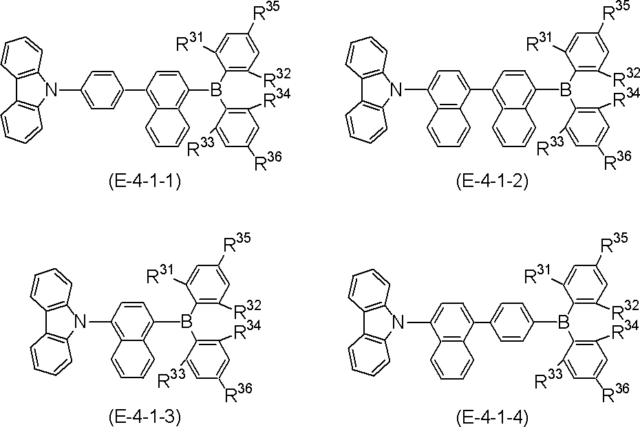
各式中、R31~R34は、それぞれ独立して、メチル、イソプロピルまたはフェニルのいずれかであり、そして、R35およびR36は、それぞれ独立して、水素、メチル、イソプロピルまたはフェニルのいずれかである。

式中、R11およびR12は、それぞれ独立して、水素原子、アルキル基、置換されていてもよいアリール基、置換シリル基、置換されていてもよい窒素含有複素環基、またはシアノ基の少なくとも一つであり、R13~R16は、それぞれ独立して、置換されていてもよいアルキル基、または置換されていてもよいアリール基であり、X1は、置換されていてもよい炭素数20以下のアリーレン基であり、そして、nはそれぞれ独立して0~3の整数である。

式中、R31~R34は、それぞれ独立して、メチル、イソプロピルまたはフェニルのいずれかであり、そして、R35およびR36は、それぞれ独立して、水素、メチル、イソプロピルまたはフェニルのいずれかである。
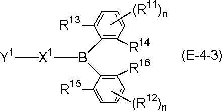
式中、R11およびR12は、それぞれ独立して、水素原子、アルキル基、置換されていてもよいアリール基、置換シリル基、置換されていてもよい窒素含有複素環基、またはシアノ基の少なくとも一つであり、R13~R16は、それぞれ独立して、置換されていてもよいアルキル基、または置換されていてもよいアリール基であり、X1は、置換されていてもよい炭素数10以下のアリーレン基であり、Y1は、置換されていてもよい炭素数14以下のアリール基であり、そして、nはそれぞれ独立して0~3の整数である。

各式中、R31~R34は、それぞれ独立して、メチル、イソプロピルまたはフェニルのいずれかであり、そして、R35およびR36は、それぞれ独立して、水素、メチル、イソプロピルまたはフェニルのいずれかである。
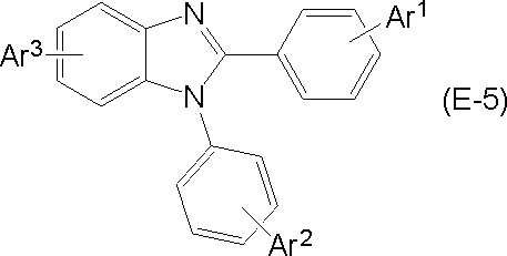
式中、Ar1~Ar3はそれぞれ独立に水素または置換されてもよい炭素数6~30のアリールである。特に、Ar1が置換されてもよいアントリルであるベンゾイミダゾール誘導体が好ましい。
陰極108は、電子注入層107および電子輸送層106を介して、発光層105に電子を注入する役割を果たすものである。
以上の正孔注入層、正孔輸送層、発光層、電子輸送層および電子注入層に用いられる材料は単独で各層を形成することができるが、高分子結着剤としてポリ塩化ビニル、ポリカーボネート、ポリスチレン、ポリ(N-ビニルカルバゾール)、ポリメチルメタクリレート、ポリブチルメタクリレート、ポリエステル、ポリスルホン、ポリフェニレンオキサイド、ポリブタジエン、炭化水素樹脂、ケトン樹脂、フェノキシ樹脂、ポリアミド、エチルセルロース、酢酸ビニル樹脂、ABS樹脂、ポリウレタン樹脂などの溶剤可溶性樹脂や、フェノール樹脂、キシレン樹脂、石油樹脂、ユリア樹脂、メラミン樹脂、不飽和ポリエステル樹脂、アルキド樹脂、エポキシ樹脂、シリコーン樹脂などの硬化性樹脂などに分散させて用いることも可能である。
有機電界発光素子を構成する各層は、各層を構成すべき材料を蒸着法、抵抗加熱蒸着、電子ビーム蒸着、スパッタリング、分子積層法、印刷法、スピンコート法またはキャスト法、コーティング法などの方法で薄膜とすることにより、形成することができる。このようにして形成された各層の膜厚については特に限定はなく、材料の性質に応じて適宜設定することができるが、通常2nm~5000nmの範囲である。膜厚は通常、水晶発振式膜厚測定装置などで測定できる。蒸着法を用いて薄膜化する場合、その蒸着条件は、材料の種類、膜の目的とする結晶構造および会合構造などにより異なる。蒸着条件は一般的に、ボート加熱温度50~400℃、真空度10-6~10-3Pa、蒸着速度0.01~50nm/秒、基板温度-150~+300℃、膜厚2nm~5μmの範囲で適宜設定することが好ましい。
また、本発明は、有機電界発光素子を備えた表示装置または有機電界発光素子を備えた照明装置などにも応用することができる。
有機電界発光素子を備えた表示装置または照明装置は、本実施形態にかかる有機電界発光素子と公知の駆動装置とを接続するなど公知の方法によって製造することができ、直流駆動、パルス駆動、交流駆動など公知の駆動方法を適宜用いて駆動することができる。
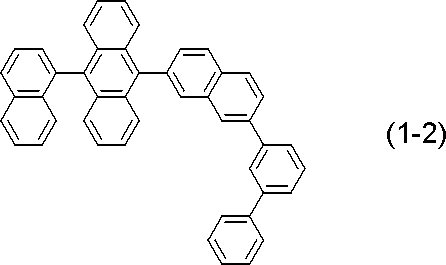
まず、窒素雰囲気下、2,7-ナフタレンジオール(48.1g)およびピリジン(380ml)をフラスコに入れ、0℃まで冷却した後、トリフルオロメタンスルホン酸無水物(203.1g)をゆっくり滴下した。その後、反応液を0℃で1時間、室温で2時間攪拌した。次に、反応液に水を加え、トルエンで目的成分を抽出し、有機層を減圧濃縮して得られた粗製品を、シリカゲルでカラム精製(溶媒:へプタン/トルエン=6/1(容量比))を行い、第1の中間体化合物であるナフタレン-2,7-ジイル ビス(トリフルオロメタンスルホナート)(112.4g)を得た。下記「反応1」にそのスキームを示す。

窒素雰囲気下、上記反応1で得られた第1の中間体化合物であるナフタレン-2,7-ジイル-ビス(トリフルオロメタンスルホナート)(25.5g)、m-ビフェニルボロン酸(11.9g)、テトラキス(トリフェニルホスフィン)パラジウム(0)(Pd(PPh3)4)(1.39g)、リン酸カリウム(25.5g)およびテトラヒドロフラン(THF)とイソプロピルアルコール(IPA)との混合溶媒(100ml)(THF/IPA=4/1(容量比))をフラスコに入れ、4時間還流した。加熱終了後に反応液を冷却し、水を加え、トルエンで目的成分を抽出した。さらに、有機層を減圧濃縮して得られた粗製品をシリカゲルでカラム精製(溶媒:ヘプタン)を行い、第2の中間体化合物である7-([1,1’-ビフェニル]-3-イル)ナフタレン-2-イル トリフルオロメタンスルホナート(14.8g)を得た。下記「反応2」にそのスキームを示す。

窒素雰囲気下、第2の中間体化合物である7-([1,1’-ビフェニル]-3-イル)ナフタレン-2-イル トリフルオロメタンスルホナート(1.50g)、(10-(ナフタレン-1-イル)アントラセン-9-イル)ボロン酸(1.22g)、テトラキス(トリフェニルホスフィン)パラジウム(0)(Pd(PPh3)4)(0.12g)、リン酸カリウム(1.49g)および1,2,4-トリメチルベンゼン(シュードクメン)、IPAおよび水の混合溶媒13ml(シュードクメン/IPA/水=10/2/1(容量比))をフラスコに入れて、5時間還流した。加熱終了後に反応液を冷却し、トルエンおよび水を加え分液した。有機層を減圧留去し得られた固体をメタノールで洗浄した後、活性炭カラムクロマトグラフィー(溶媒:トルエン)で精製し、目的の式(1-2)で表される化合物である9-(7-([1,1’-ビフェニル]-3-イル)ナフタレン-2-イル)-10-(ナフタレン-1-イル)アントラセン(0.7g)を得た。下記「反応3」にそのスキームを示す。(10-(ナフタレン-1-イル)アントラセン-9-イル)ボロン酸は市販品を使用した。
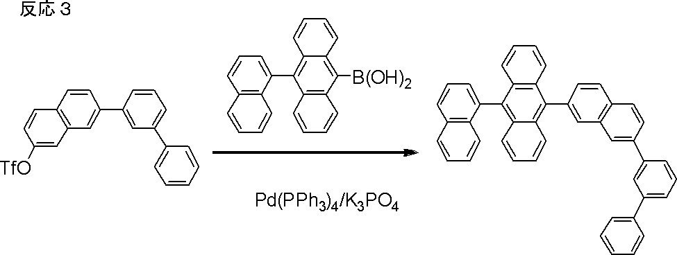
1H-NMR(CDCl3):δ=8.19(d,1H)、8.07~8.17(m,4H)、8.03(d,1H)、7.99(m,1H)、7.94(d,1H)、7.80(d,2H)、7.56~7.78(m,8H)、7.45~7.52(m,5H)、7.38(m,1H)、7.32(m,2H)、7.20-7.28(m,4H).
[測定機器:Diamond DSC (PERKIN-ELMER社製); 測定条件: 冷却速度200℃/Min.、昇温速度10℃/Min.]

窒素雰囲気下、(10-(ナフタレン-1-イル)アントラセン-9-イル)ボロン酸(25.1g)、7-メトキシナフタレン-2-イル トリフルオロメタンスルホナート(24.3g)、Pd(PPh3)4(0.9g)、リン酸カリウム(30.6g)およびシュードクメン、IPAおよび水の混合溶媒260ml(シュードクメン/IPA/水=8/4/1(容量比))をフラスコに入れて、4.5時間還流した。加熱終了後に水を加え、室温まで冷却し、吸引濾過にて固体を採取した。得られた固体を水、次いでメタノールで洗浄した後、トルエンに溶解させ、シリカゲルショートカラムで精製した。溶媒をゆっくり減圧留去することで得られる結晶を、吸引濾過にて採取し、第3の中間体化合物である9-(7-メトキシナフタレン-2-イル)-10-(ナフタレン-1-イル)アントラセン(17.5g)を得た。下記「反応4」にそのスキームを示す。
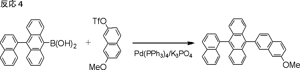
窒素雰囲気下、第3の中間体化合物である9-(7-メトキシナフタレン-2-イル)-10-(ナフタレン-1-イル)アントラセン(17.5)、ピリジン塩酸塩(22.0g)およびN-メチルピロリドン(35ml)をフラスコに入れて、200℃で6時間半撹拌した。加熱終了後、100℃以下まで冷却し、水を加えて析出した固体を吸引濾過にて採取した。得られた粗製品をシリカゲルカラムクロマトグラフィー(溶媒:トルエン)で精製し、第4の中間体化合物である7-(10-(ナフタレン-1-イル)アントラセン-9-イル)ナフタレン-2-オール(16.0g)を得た。下記「反応5」にそのスキームを示す。
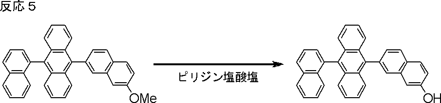
窒素雰囲気下、第4の中間体化合物である7-(10-(ナフタレン-1-イル)アントラセン-9-イル)ナフタレン-2-オール(16.0g)およびピリジン(150ml)をフラスコに入れ、0℃まで冷却した後、トリフルオロメタンスルホン酸無水物(15.2g)をゆっくり滴下した。その後、室温で3時間攪拌した後。再び0℃まで冷却し、水を加え反応を停止し、トルエンで目的成分を抽出した。有機層を減圧濃縮して得られた粗製品を、シリカゲルでカラム精製(溶媒:トルエン)を行い、第5の中間体化合物である7-(10-(ナフタレン-1-イル)アントラセン-9-イル)ナフタレン-2-イル トリフルオロメタンスルホナート(20.0g)を得た。下記「反応6」にそのスキームを示す。

窒素雰囲気下、第5の中間体化合物である7-(10-(ナフタレン-1-イル)アントラセン-9-イル)ナフタレン-2-イル トリフルオロメタンスルホナート(3.0g)、フェニルボロン酸(0.8g)、ビス(ジベンジリデンアセトン)パラジウム(0)(Pd(dba)2)(0.03g)、トリシクロヘキシルホスフィン(PCy3)(0.03g)、リン酸カリウム(2.2g)およびトルエン、エタノールおよび水の混合溶媒22ml(トルエン/エタノール/水=9/1/1(容量比))をフラスコに入れて、2時間半還流した。加熱終了後に反応液を室温まで冷却し、メタノールを加え、析出物を吸引濾過にて採取した。得られた固体を水、次いでメタノールで洗浄後、更に酢酸エチルで洗浄した。得られた粗製品をトルエンに溶解させ、活性炭ショートカラムに通すことで着色成分を除去し、クロロベンゼンから再結晶することで、目的の式(1-1)で表される化合物である9-(ナフタレン-1-イル)-10-(7-フェニルナフタレン-2-イル)アントラセン(1.2g)を得た。下記「反応7」にそのスキームを示す。

1H-NMR(CDCl3):δ=8.07~8.17(m,5H)、8.04(d,1H)、7.89(dd,1H)、7.76~7.82(m,4H)、7.65~7.75(m,2H)、7.61(d,1H)、7.46~7.54(m,5H)、7.41(m,1H)、7.29~7.33(m,2H)、7.20-7.28(m,4H).
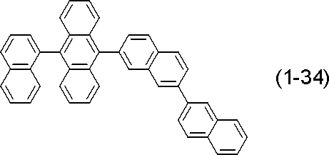
窒素雰囲気下、第5の中間体化合物である7-(10-(ナフタレン-1-イル)アントラセン-9-イル)ナフタレン-2-イル トリフルオロメタンスルホナート(3.0g)、2-ナフタレンボロン酸(1.0g)、(Pd(dba)2)(0.03g)、トリシクロヘキシルホスフィン(0.03g)、リン酸カリウム(2.2g)およびトルエン、エタノールおよび水の混合溶媒22ml(トルエン/エタノール/水=9/1/1(容量比))をフラスコに入れて、3時間還流した。加熱終了後に反応液を室温まで冷却し、メタノールを加え、析出物を吸引濾過にて採取した。得られた固体を水、次いでメタノールで洗浄後、更に酢酸エチルで洗浄した。得られた粗製品をクロロベンゼンに溶解させ、活性炭ショートカラムに通すことで着色成分を除去し、更にクロロベンゼンから再結晶することで、目的の式(1-34)で表される化合物である9-([2、2’-ビナフタレン]-7-イル)-10-(ナフタレン-1-イル)アントラセン(1.5g)を得た。下記「反応8」にそのスキームを示す。
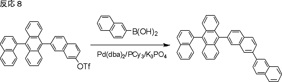
1H-NMR(CDCl3):δ=8.26(dd,1H)、8.24(s,1H)、8.11~8.18(m,3H)、8.08(d,1H)、7.88~8.05(m,6H)、7.81(dd,2H)、7.66~7.75(m,2H)、7.61(d,1H)、7.46~7.56(m,5H)、7.29~7.34(m,2H)、7.20-7.28(m,4H).
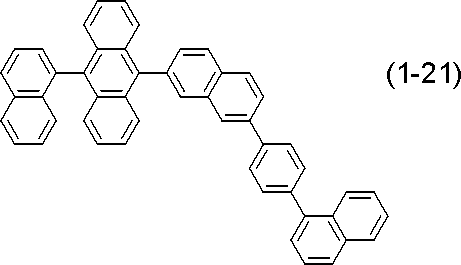
窒素雰囲気下、第5の中間体化合物である7-(10-(ナフタレン-1-イル)アントラセン-9-イル)ナフタレン-2-イル トリフルオロメタンスルホナート(3.0g)、(4-(ナフタレン-1-イル)フェニル)ボロン酸(1.9g)、ビス(ジベンジリデンアセトン)パラジウム(0)(Pd(dba)2)(0.03g)、トリシクロヘキシルホスフィン(0.03g)、リン酸カリウム(2.2g)およびトルエン、エタノールおよび水の混合溶媒22ml(トルエン/エタノール/水=9/1/1(容量比))をフラスコに入れて、6時間半還流した。加熱終了後に反応液を室温まで冷却し、メタノールを加え、析出物を吸引濾過にて採取した。得られた固体を水、次いでメタノールで洗浄後、更に酢酸エチルで洗浄した。得られた粗製品をトルエンに溶解させ、活性炭ショートカラムに通すことで着色成分を除去した。溶媒を減圧留去し、得られた油状物質に酢酸エチルを加えることで析出した沈殿を吸引濾過にて採取し、目的の式(1-21)で表される化合物である9-(ナフタレン-1-イル)-10-(7-(ナフタレン-1-イル)フェニル)ナフタレン-2-イル)アントラセン(2.6g)を得た。下記「反応9」にそのスキームを示す。

1H-NMR(CDCl3):δ=8.24(d,1H)、8.12~8.19(m,3H)、8.09(d,1H)、8.03(m,2H)、7.99(dd,1H)、7.88~7.96(m,4H)、7.83(d,2H)、7.64~7.76(m,4H)、7.62(d,1H)、7.46~7.59(m,7H)、7.31~7.35(m,2H)、7.20-7.28(m,4H).

窒素雰囲気下、第5の中間体化合物である7-(10-(ナフタレン-1-イル)アントラセン-9-イル)ナフタレン-2-イル トリフルオロメタンスルホナート(3.0g)、2-トリフェニレンボロン酸(2.1g)、Pd(dba)2(0.03g)、トリシクロヘキシルホスフィン(0.03g)、リン酸カリウム(2.2g)およびトルエン、エタノールおよび水の混合溶媒22ml(トルエン/エタノール/水=9/1/1(容量比))をフラスコに入れて、2時間還流した。加熱終了後に反応液を室温まで冷却し、メタノールを加え、析出物を吸引濾過にて採取した。得られた固体を水、次いでメタノールで洗浄後、更に酢酸エチルで洗浄した。得られた粗製品をクロロベンゼンに溶解させ、活性炭ショートカラムに通すことで着色成分を除去し、更にクロロベンゼンから再結晶することで、目的の式(1-38)で表される化合物である2-(7-(10-(ナフタレン-1-イル)アントラセン-9-イル)ナフタレン-2-イル)トリフェニレン(1.9g)を得た。下記「反応10」にそのスキームを示す。

1H-NMR(CDCl3):δ=9.75(s,1H)、8.68~8.90(m,6H)、8.38(m,1H)、8.02~8.30(m,8H)、7.60~7.90(m,10H)、7.53(m,3H)、7.35(m,3H).
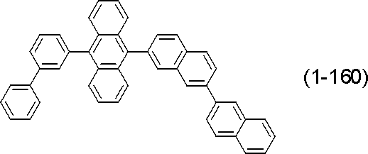
窒素雰囲気下、2-ナフタレンボロン酸(33.7g)、ナフタレン-2,7-ジイル-ビス(トリフルオロメタンスルホナート)(50.0g)、Pd(PPh3)4(5.7g)、リン酸カリウム(69.3g)およびトルエンおよびエタノールの混合溶媒400ml(トルエン/エタノール=5/1(容量比))をフラスコに入れて、7時間還流した。加熱終了後に反応液を冷却し、水を加え、トルエンで目的成分を抽出した。次いで、有機層を減圧濃縮し、シリカゲルカラムカラムクロマトグラフィー(溶媒:トルエン)にて精製を行い、第6の中間体化合物である7-メトキシ-2,2’-ビナフタレン(32.0g)を得た。下記「反応11」にそのスキームを示す。
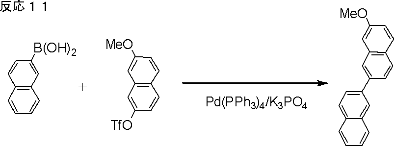
窒素雰囲気下、第6の中間体化合物である7-メトキシ-2,2’-ビナフタレン(31.0)、ピリジン塩酸塩(63.0g)およびN-メチルピロリドン(20ml)をフラスコに入れて、200℃で7時間撹拌した。加熱終了後、100℃以下まで冷却し、水を加えて析出した固体を吸引濾過にて採取した。得られた固体をシリカゲルカラムクロマトグラフィー(溶媒:トルエン)で精製し、第7の中間体化合物である[2,2’-ビナフタレン]-7-オール(22.0g)を得た。下記「反応12」にそのスキームを示す。

窒素雰囲気下、第7の中間体化合物である[2,2’-ビナフタレン]-7-オール(20.0g)およびピリジン(200ml)をフラスコに入れ、0℃まで冷却した後、トリフルオロメタンスルホン酸無水物(30.2g)をゆっくり滴下した。その後、室温で2時間攪拌した後。再び0℃まで冷却し、水を加え反応を停止し、トルエンで目的成分を抽出した。次いで、有機層を減圧濃縮し、シリカゲルカラムクロマトグラフィー(溶媒:トルエン)にて精製した。得られた粗製品をアセトンに溶解させ、ヘプタンを加えることで再沈殿をおこない、第8の中間体化合物である[2,2’-ビナフタレン]-7-イル トリフルオロメタンスルホナート(16.2g)を得た。下記「反応13」にそのスキームを示す。

窒素雰囲気下、第8の中間体化合物である[2,2’-ビナフタレン]-7-イル トリフルオロメタンスルホナート(16.0g)、アントラセン-9-イルボロン酸(13.3g)、Pd(dba)2(0.7g)、トリシクロヘキシルホスフィン(0.8g)、リン酸カリウム(16.9g)およびトルエンおよびエタノールの混合溶媒120ml(トルエン/エタノール=4/1(容量比))をフラスコに入れて、2時間半還流した。加熱終了後に反応液を冷却し、水およびトルエンを加え分液した。次いで有機層を減圧留去し得られた粗製品をシリカゲルカラムクロマトグラフィー(溶媒:トルエン)で精製した。溶媒を減圧留去し得られた固体をヘプタンで洗浄し、第9の中間体化合物である9-([2,2’-ビナフタレン]-7-イル)アントラセン(10.0g)を得た。下記「反応14」にそのスキームを示す。
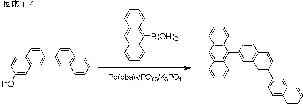
窒素雰囲気下、第9の中間体化合物である9-([2,2’-ビナフタレン]-7-イル)アントラセン(10.0g)、N-ブロモスクシンイミド(NBS)(4.6g)、ヨウ素(0.1g)およびTHF(60ml)をフラスコにいれて、室温で終夜撹拌した。チオ硫酸ナトリウム水溶液を加え、反応を停止し、水およびトルエンを加え分液した。次いで有機層を減圧留去し得られた固体をシリカゲルカラムクロマトグラフィー(溶媒:トルエン)で精製した。溶媒を減圧留去し得られた固体をヘプタンで洗浄し、第10の中間体化合物である[9-([2,2’-ビナフタレン]-7-イル)-10-ブロモアントラセン(11.0g)を得た。下記「反応15」にそのスキームを示す。
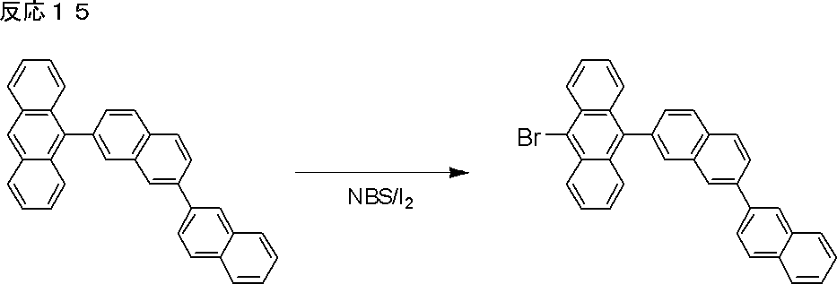
窒素雰囲気下、第10の中間体化合物である[9-([2,2’-ビナフタレン]-7-イル)-10-ブロモアントラセン(2.0g)、m-ビフェニルボロン酸(1.4g)、Pd(PPh3)4)(0.1g)、リン酸カリウム(1.7g)およびトルエンおよびエタノールの混合溶媒16ml(トルエン/エタノール=4/1(容量比))をフラスコに入れて、10時間還流した。加熱終了後に反応液を室温まで冷却し、水を加え、析出物を吸引濾過にて採取した。得られた固体を水、次いでメタノールで洗浄後、更に酢酸エチルで洗浄した。得られた粗製品をシリカゲルカラムクロマトグラフィー(溶媒:クロロベンゼン)で精製し、最後にクロロベンゼンから再結晶することで、目的の式(1-160)で表される化合物である9-([1,1’-ビフェニル]-3-イル)-10-([2,2’-ビナフタレン]-7-イル)アントラセン(0.5g)を得た。下記「反応16」にそのスキームを示す。

1H-NMR(CDCl3):δ=8.24(d,2H)、8.14(t,2H)、8.09(m,1H)、7.88~8.15(m,5H)、7.76~7.84(m,6H)、7.71(m,3H)、7.64(m,1H)、7.44~7.56(m,5H)、7.32~7.38(m,5H).

窒素雰囲気下、第10の中間体化合物である[9-([2,2’-ビナフタレン]-7-イル)-10-ブロモアントラセン(2.0g)、[1,1’:3’,1’’-テルフェニル]-5’-イルボロン酸(1.0g)、Pd(dba)2(0.03g)、トリシクロヘキシルホスフィン(0.03g)、リン酸カリウム(1.3g)およびトルエンおよびエタノールの混合溶媒20ml(トルエン/エタノール=4/1(容量比))をフラスコに入れて、2時間還流した。加熱終了後に反応液を室温まで冷却し、水を加え反応を停止し、トルエンで目的物を抽出した。溶媒を減圧留去し、得られた粗製品をシリカゲルカラムクロマトグラフィー(溶媒:トルエン)で精製し、更に活性炭カラムクロマトグラフィー(溶媒:トルエン)で精製することで、目的の式(1-162)で表される化合物である9-([1,1’:3’,1’’-テルフェニル]-5’-イル)-10-([2,2’-ビナフタレン]-7-イル)アントラセン(1.0g)を得た。下記「反応17」にそのスキームを示す。

1H-NMR(CDCl3):δ=8.22~8.27(m,2H)、8.14(t,2H)、8.09(s,1H)、8.05(m,1H)、8.02(dd,1H)、7.88~8.00(m,6H)、7.76~7.81(m,8H)、7.65(dd,1H)、7.46~7.55(m,6H)、7.33~7.41(m,6H).

窒素雰囲気下、第10の中間体化合物である[9-([2,2’-ビナフタレン]-7-イル)-10-ブロモアントラセン(2.0g)、フェナントレン-9-イルボロン酸(1.1g)、酢酸パラジウム(Pd(OAc)2)(0.06g)、2-ジシクロヘキシルホスフィノ-2’,6’-ジメトキシビフェニル(SPhos、アルドリッチ製)(0.02g)、リン酸カリウム(1.7g)およびトルエンおよびエタノールの混合溶媒10ml(トルエン/エタノール=4/1(容量比))をフラスコに入れて、10時間還流した。加熱終了後に反応液を室温まで冷却し、水を加え、析出物を吸引濾過にて採取した。得られた固体を水、次いでメタノールで洗浄後、シリカゲルカラムクロマトグラフィー(溶媒:トルエン)で精製した。更にクロロベンゼンから再結晶することで、目的の式(1-164)で表される化合物である9-([2,2’-ビナフタレン]-7-イル)-10-(フェナントレン-9-イル)アントラセン(0.7g)を得た。下記「反応18」にそのスキームを示す。
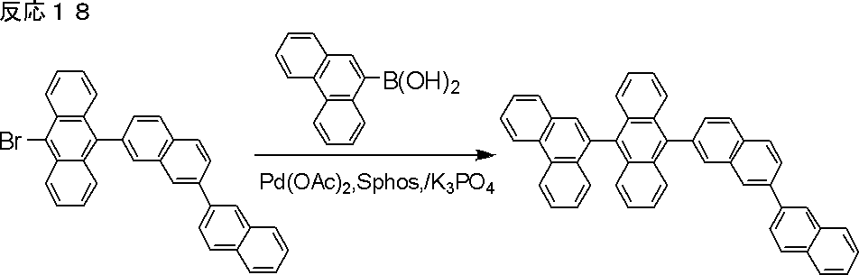
1H-NMR(CDCl3):δ=8.90(m,2H)、8.28(m,1H)、8.25(s,1H)、8.13~8.20(m,3H)、7.89~8.04(m,7H)、7.83(d,2H)、7.66~7.81(m,4H)、7.62(d,2H)、7.53(m,2H)、7.28~7.38(m,4H)、7.23(m,2H).
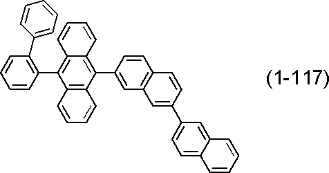
窒素雰囲気下、第10の中間体化合物である[9-([2,2’-ビナフタレン]-7-イル)-10-ブロモアントラセン(2.0g)、o-ビフェニルボロン酸(0.9g)、Pd(OAc)2(0.03g)、SPhos(アルドリッチ製)(0.12g)、リン酸カリウム(1.7g)およびシュードクメン、t-ブチルアルコールおよび水の混合溶媒14ml(シュードクメン/t-ブチルアルコール/水=10/3/1(容量比))をフラスコに入れて、8時間還流した。加熱終了後に反応液を室温まで冷却し、水を加え反応を停止し、トルエンで抽出した。溶媒を減圧留去し、得られた固体をシリカゲルカラムクロマトグラフィー(溶媒:トルエン)で精製し、更に活性炭カラムクロマトグラフィー(溶媒:トルエン)で精製することで、目的の式(1-117)で表される化合物である9-([1,1’-ビフェニル]-2-イル)-10-([2,2’-ビナフタレン]-7-イル))アントラセン(0.5g)を得た。下記「反応19」にそのスキームを示す。

1H-NMR(CDCl3):δ=8.21(m,2H)、8.12(d,1H)、8.08(dd,1H)、7.87~8.03(m,6H)、7.71(d,2H)、7.67(m,4H)、7.45~7.59(m,5H)、7.23~7.32(m,4H)、7.03(m,2H)、6.88~6.97(m,3H).
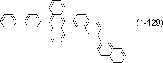
窒素雰囲気下、第10の中間体化合物である[9-([2,2’-ビナフタレン]-7-イル)-10-ブロモアントラセン(2.0g)、p-ビフェニルボロン酸(0.9g)、Pd(dba)2(0.05g)、トリシクロヘキシルホスフィン(0.05g)、リン酸カリウム(1.7g)およびトルエンおよびエタノールの混合溶媒15ml(トルエン/エタノール=4/1(容量比))をフラスコに入れて、3時間還流した。加熱終了後に反応液を室温まで冷却し、水を加え、析出物を吸引濾過にて採取した。得られた固体を水、次いでメタノールで洗浄後、シリカゲルカラムクロマトグラフィー(溶媒:トルエン)で精製し、更に活性炭カラムクロマトグラフィー(溶媒:トルエン)で精製することで、目的の式(1-129)で表される化合物である9-([1,1’-ビフェニル]-4-イル)-10-([2,2’-ビナフタレン]-7-イル))アントラセン(0.6g)を得た。下記「反応20」にそのスキームを示す。
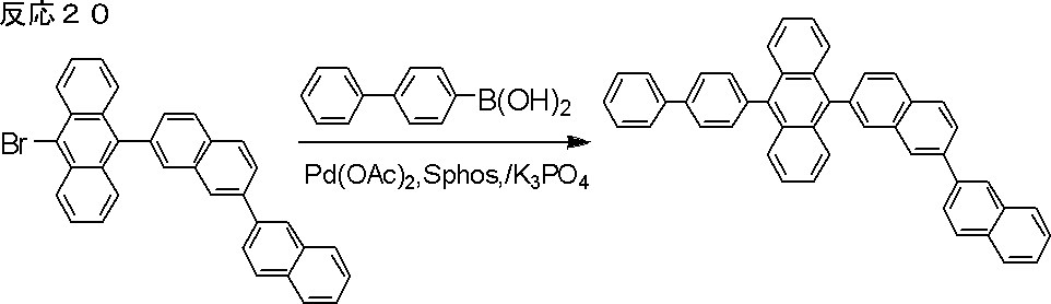
1H-NMR(CDCl3):δ=8.24(d,2H)、8.12(t,2H)、8.09(s,1H)、7.88~8.03(m,5H)、7.86(d,2H)、7.83(d,2H)、7.79(m,4H)、7.64(dd,1H)、7.60(d,2H)、7.48~7.56(m,4H)、7.43(t,1H)、7.33-7.40(m,4H).
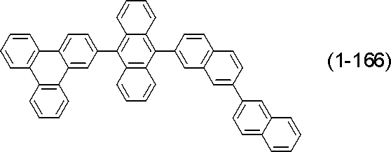
窒素雰囲気下、トリフェニレン-2-イルボロン酸(5.6g)、9-ブロモアントラセン(3.5g)、(Pd(PPh3)4)(0.5g)、リン酸カリウム(5.8g)およびシュードクメン、t-ブチルアルコールおよび水の混合溶媒48ml(シュードクメン/t-ブチルアルコール/水=10/1/1(容量比))をフラスコに入れて、8時間還流した。水を加え、析出物を吸引濾過にて採取した。得られた固体を水、次いでメタノールで洗浄後、シリカゲルカラムクロマトグラフィー(溶媒:トルエン)で精製した。次いでトルエン/酢酸エチル混合溶液から再結晶することで、第11の中間体化合物である2-(アントラセン-9-イル)トリフェニレン(3.3g)を得た。下記「反応21」にそのスキームを示す。
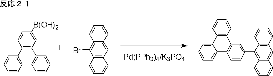
窒素雰囲気下、第11の中間体化合物である2-(アントラセン-9-イル)トリフェニレン(3.3g)、N-ブロモスクシンイミド(NBS)(1.7g)、ヨウ素(0.1g)およびTHF(25ml)をフラスコにいれて、室温で5時間撹拌した。チオ硫酸ナトリウム水溶液を加え、反応を停止し、析出物を吸引濾過にて採取した。得られた固体をメタノール、次いでヘプタンで洗浄後、シリカゲルカラムクロマトグラフィー(溶媒:トルエン)で精製し、第12の中間体化合物である2-(10-ブロモアントラセン-9-イル)トリフェニレン(3.5g)を得た。下記「反応22」にそのスキームを示す。

窒素雰囲気下、第12の中間体化合物である2-(10-ブロモアントラセン-9-イル)トリフェニレン(3.5g)、ビスピナコラートジボロン(2.2g)、PdCl2(dppf)(0.2g)、炭酸カリウム(2.0g)、酢酸カリウム(1.4g)およびシクロペンチルメチルエーテル(20ml)をフラスコに入れて、5時間還流した。反応液を室温まで冷却した後、水およびトルエンを加え分液した。溶媒を減圧留去し得られた粗製品を活性炭カラムクロマトグラフィー(溶媒:トルエン)で精製し、第13の中間体化合物である4,4,5,5-テトラメチル-2-(10-(トリフェニレン-2-イル)アントラセン-9-イル)-1,3,2-ジオキサボロラン(2.0g)を得た。下記「反応23」にそのスキームを示す。

窒素雰囲気下、第13の中間体化合物である4,4,5,5-テトラメチル-2-(10-(トリフェニレン-2-イル)アントラセン-9-イル)-1,3,2-ジオキサボロラン(1.5g)、[2,2’-ビナフタレン]-7-イル トリフルオロメタンスルホナート(1.3g)、Pd(PPh3)4(0.2g)、リン酸カリウム(1.2g)およびトルエン、エタノールおよび水の混合溶媒11ml(トルエン/エタノール/水=8/2/1(容量比))をフラスコに入れて、4時間還流した。加熱終了後に反応液を室温まで冷却し、水を加え、析出物を吸引濾過にて採取した。得られた固体を水、次いでメタノールで洗浄後、クロロベンゼンに溶解させ、活性アルミナカラムクロマトグラフィー(溶媒:トルエン)を通した。更にクロロベンゼンから再結晶することで、目的の式(1-166)で表される化合物である2-(10-([2,2’-ビナフタレン]-7-イル)アントラセン-9-イル)トリフェニレン(0.9g)を得た。下記「反応24」にそのスキームを示す。
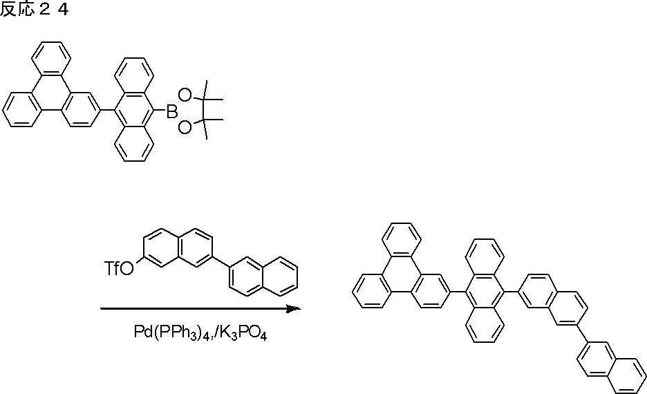
1H-NMR(CDCl3):δ=8.93(d,1H)、8.83(m,2H)、8.74(m,2H)、8.61(d,1H)、8.28(m,1H)、8.24(m,1H)、8.15(m,3H)、7.90~8.05(m,5H)、7.80~7.87(m,5H)、7.76(m,2H)、7.69(m,2H)、7.61(t,1H)、7.52(m,2H)、7.36(m,4H).
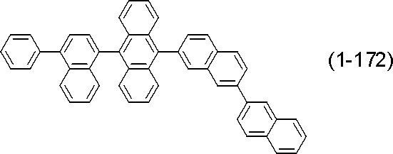
9-ブロモアントラセン(75.0g)、(4-エトキシナフタレン-1-イル)ボロン酸(78.0g)、Pd(dba)2(5.0g)、トリシクロヘキシルホスフィン(4.9g)、リン酸カリウム(124.0g)およびシュードクメンおよびt-ブチルアルコールの混合溶媒440ml(シュードクメン/t-ブチルアルコール=10/1(容量比))をフラスコに入れて、8時間還流した。反応液を室温まで冷却した後、析出した固体を吸引ろ過にて採取し、その固体をEDTA・4Na水溶液、水、メタノールの順で洗浄した。次いで加熱したクロロベンゼンに溶かし、シリカゲルを敷いた桐山ロートで吸引ろ過を行なった。ろ液を減圧留去して得られた粗製品をヘプタンで加熱洗浄し、第14の中間体化合物である9-(4-エトキシナフタレン-1-イル)アントラセン(87.1g)を得た。下記「反応25」にそのスキームを示す。
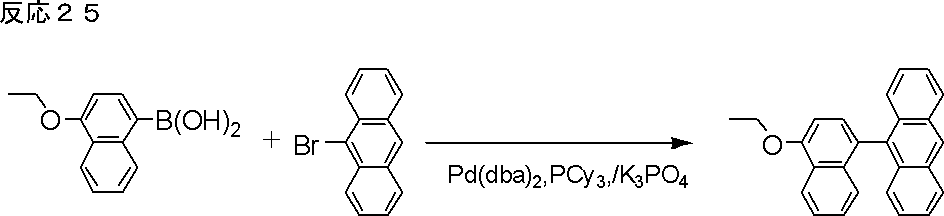
窒素雰囲気下、第14の中間体化合物である9-(4-エトキシナフタレン-1-イル)アントラセン(87.1g)、ピリジン塩酸塩(289.0g)および1-メチル-2-ピロリドン(87ml)をフラスコに入れ、175℃で16時間攪拌した。反応液を室温まで冷却した後、水を加え加熱洗浄を行い、吸引ろ過にて溶け残った固体を採取した。得られた固体をメタノールで加熱洗浄後、加熱したクロロベンゼンに溶かし、シリカゲルを敷いた桐山ロートで吸引ろ過を行なった。ろ液を適量減圧留去した後、ヘプタンを加えることで再沈殿を行い、第15の中間体化合物である4-(アントラセン-9-イル)ナフタレン-1-オール(74.3g)得た。下記「反応26」にそのスキームを示す。

窒素雰囲気下、第15の中間体化合物である4-(アントラセン-9-イル)ナフタレン-1-オール(74.0g)およびピリジン(500ml)の入ったフラスコを、氷浴で冷却し、トリフルオロメタンスルホン酸無水物(98.0g)を滴下した。滴下終了後、室温で1時間撹拌した後、水を加え、析出した固体を吸引ろ過にて採取した。得られた固体をメタノールで洗浄した後、トルエンに溶かし、シリカゲルを敷いた桐山ロートで吸引ろ過を行なった。ろ液を減圧留去して得られた粗製品を、ヘプタンから再結晶し、第16の中間体化合物である4-(アントラセン-9-イル)ナフタレン-1-イル トリフルオロメタンスルホナート(100.2g)を得た。下記「反応27」にそのスキームを示す。
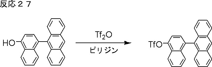
窒素雰囲気下、第16の中間体化合物である4-(アントラセン-9-イル)ナフタレン-1-イル トリフルオロメタンスルホナート(30.0g)、フェニルボロン酸(12.1g)、Pd(PPh3)4(2.3g)、リン酸カリウム(28.1g)およびシュードクメン、t-ブチルアルコールおよび水の混合溶媒150ml(シュードクメン/t-ブチルアルコール/水=8/1/1(容量比))をフラスコに入れて、5時間半還流した。加熱終了後に反応液を室温まで冷却し、水を加え反応を停止し、トルエンで抽出した。溶媒を減圧留去した後、シリカゲルカラムクロマトグラフィー(溶媒:ヘプタン/トルエン混合溶媒)で精製した。この際、「有機化学実験のてびき(1)-物質取扱法と分離精製法-」株式会社化学同人出版、94頁に記載の方法を参考にして、展開液中のトルエンの比率を徐々に増加させて目的物を溶出させた。溶媒を減圧留去して得られた粗製品をヘプタン、次いでメタノールで洗浄し、第17の中間体化合物である9-(4-フェニルナフタレン-1-イル)アントラセン(24.1g)を得た。下記「反応28」にそのスキームを示す。

窒素雰囲気下、第17の中間体化合物である9-(4-フェニルナフタレン-1-イル)アントラセン(24.0g)、N-ブロモスクシンイミド(NBS)(13.5g)、ヨウ素(0.1g)およびTHF(200ml)をフラスコにいれて、室温で3時間半撹拌した。チオ硫酸ナトリウム水溶液を加え、反応を停止し、酢酸エチルで抽出した。次いで溶媒を減圧留去し、途中で析出する固体を吸引濾過にて採取した。得られた粗製品をメタノールで洗浄し、第18の中間体化合物である9-ブロモ-10-(4-フェニルナフチル-1-イル)アントラセン(26.2g)を得た。下記「反応29」にそのスキームを示す。
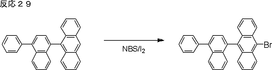
窒素雰囲気下、第18の中間体化合物である9-ブロモ-10-(4-フェニルナフチル-1-イル)アントラセン(26.0g)、ビスピナコラートジボロン(17.3g)、PdCl2(dppf)(1.4g)、炭酸カリウム(15.6g)、酢酸カリウム(11.1g)およびシクロペンチルメチルエーテル(200ml)をフラスコに入れて、5時間還流した。反応液を室温まで冷却した後、トルエンを加え無機塩以外を溶解させ、吸引ろ過にて無機塩を除去した。溶媒を減圧留去し、得られた固体をヘプタンで洗浄後、シリカゲルショートカラム(溶媒:トルエン)により、着色成分を除去した。溶媒を減圧留去し、得られた油状物質にエタノールを加えることで再沈殿をさせ、第19の中間体化合物である4,4,5,5-テトラメチル-2-(10-(4-フェニルナフタレン-1-イル)アントラセン-9-イル)-1,3,2-ジオキサボロラン(26.6g)を得た。下記「反応30」にそのスキームを示す。

窒素雰囲気下、第19の中間体化合物である4,4,5,5-テトラメチル-2-(10-(4-フェニルナフタレン-1-イル)アントラセン-9-イル)-1,3,2-ジオキサボロラン(3.0g)、[2,2’-ビナフタレン]-7-イル トリフルオロメタンスルホナート(2.6g)、Pd(PPh3)4(0.3g)、リン酸カリウム(2.5g)およびトルエン、エタノールおよび水の混合溶媒26ml(トルエン/エタノール/水=8/4/1(容量比))をフラスコに入れて、2時間還流した。加熱終了後に反応液を室温まで冷却し、水およびトルエンを加え液した。溶媒を減圧留去した後、シリカゲルカラムクロマトグラフィー(溶媒:ヘプタン/トルエン=4/1)で精製した。ここで得られた粗製品を酢酸エチルで洗浄することで、目的の式(1-172)で表される化合物である9-([2,2’-ビナフタレン]-7-イル)-10-(4-フェニルナフタレン-1-イル)アントラセン(1.7g)を得た。下記「反応31」にそのスキームを示す。

1H-NMR(CDCl3):δ=8.28(d,1H)、8.24(s,1H)、8.13~8.20(m,3H)、8.10(d,1H)、8.04(d,1H)、7.88~8.02(m,4H)、7.84(d,2H)、7.65~7.76(m,5H)、7.49~7.62(m,7H)、7.45(m,1H)、7.25-7.37(m,6H).
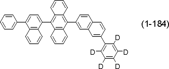
窒素雰囲気下、上記第19の中間体化合物である4,4,5,5-テトラメチル-2-(10-(4-フェニルナフタレン-1-イル)アントラセン-9-イル)-1,3,2-ジオキサボロラン(10-(ナフタレン-1-イル)アントラセン-9-イル)ボロン酸(23.0g)、7-メトキシナフタレン-2-イル トリフルオロメタンスルホナート(18.0g)、Pd(PPh3)4(1.6g)、リン酸カリウム(19.3g)およびシュードクメン、IPAおよび水の混合溶媒125ml(シュードクメン/IPA/水=20/4/1(容量比))をフラスコに入れて、5時間還流した。加熱終了後、水およびトルエンを加え分液し、溶媒を減圧留去後に得られた固体をシリカゲルカラムクロマトグラフィー(溶媒:ヘプタン/トルエン=1/1)で精製した。得られた粗製品を更にメタノールで洗浄し、第20の中間体化合物である9-(7-メトキシナフタレン-2-イル)-10-(4-フェニルナフタレン-1-イル)アントラセン(16.3g)を得た。下記「反応32」にそのスキームを示す。

窒素雰囲気下、第20の中間体化合物である9-(7-メトキシナフタレン-2-イル)-10-(4-フェニルナフタレン-1-イル)アントラセン(16.0)、ピリジン塩酸塩(17.3g)およびN-メチルピロリドン(30ml)をフラスコに入れて、200℃で8時間撹拌した。加熱終了後、100℃以下まで冷却し、水およびトルエンを加え分液した。溶媒を減圧留去した後、シリカゲルカラムクロマトグラフィー(溶媒:トルエン)で精製し、第21の中間体化合物である7-(10-(4-フェニルナフタレン-1-イル)アントラセン-9-イル)ナフタレン-2-オール(15.5g)を得た。下記「反応33」にそのスキームを示す。
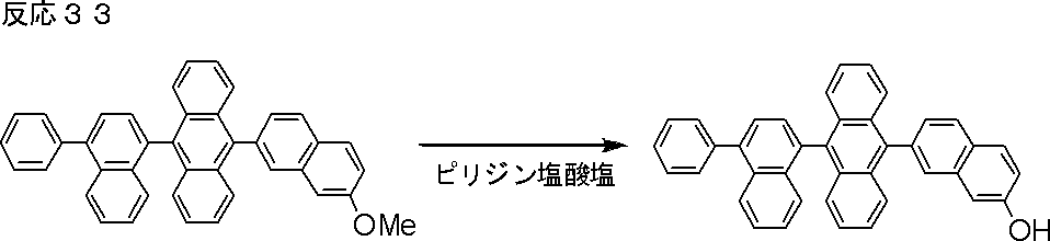
窒素雰囲気下、第21の中間体化合物である7-(10-(4-フェニルナフタレン-1-イル)アントラセン-9-イル)ナフタレン-2-オール(15.5g)およびピリジン(100ml)をフラスコに入れ、0℃まで冷却した後、トリフルオロメタンスルホン酸無水物(16.9g)をゆっくり滴下した。その後、室温で3時間攪拌した後。再び0℃まで冷却し、水を加え反応を停止し、トルエンで目的成分を抽出した。有機層を減圧濃縮した後、シリカゲルでカラム精製(溶媒:トルエン)を行い、得られた粗製品を更にヘプタンで洗浄することで、第22の中間体化合物である7-(10-(4-フェニルナフタレン-1-イル)アントラセン-9-イル)ナフタレン-2-イル トリフルオロメタンスルホナート(16.2g)を得た。下記「反応34」にそのスキームを示す。
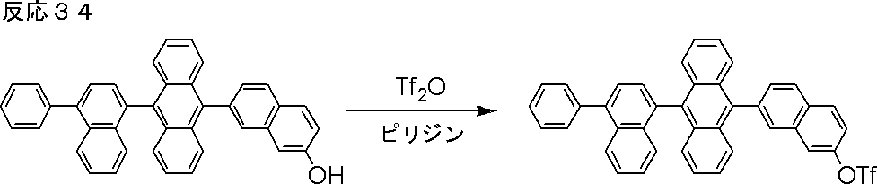
窒素雰囲気下、第22の中間体化合物である7-(10-(4-フェニルナフタレン-1-イル)アントラセン-9-イル)ナフタレン-2-イル トリフルオロメタンスルホナート(3.5g)、[2,3,4,5,6-2H5]フェニルボロン酸(1.0g)、ビス(ジベンジリデンアセトン)パラジウム(0)(Pd(dba)2)(0.03g)、トリシクロヘキシルホスフィン(PCy3)(0.03g)、リン酸カリウム(2.3g)およびトルエン、エタノールおよび水の混合溶媒22ml(トルエン/エタノール/水=9/1/1(容量比))をフラスコに入れて、3時間還流した。加熱終了後、反応液を室温まで冷却し、水およびトルエンを加え分液した。溶媒を減圧留去した後、シリカゲルカラムクロマトグラフィー(溶媒:ヘプタン/トルエン=3/1(容量比))で精製し、目的の式(1-184)で表される化合物である9-(4-フェニルナフタレン-1-イル)-10-(7-([2,3,4,5,6-2H5]フェニル)ナフタレン-2-イル)アントラセン(1.7g)を得た。下記「反応35」にそのスキームを示す。
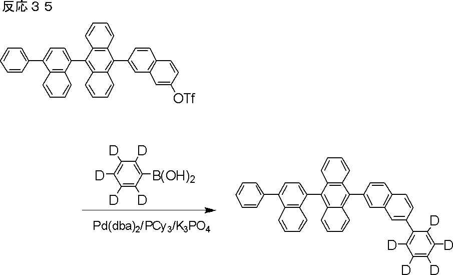
1H-NMR(CDCl3):δ=8.08~8.16(m,5H)、7.89(d,1H)、7.82(d,2H)、7.64~7.73(m,5H)、7.56~7.61(m,4H)、7.51(t,1H)、7.44(t,1H)、7.23-7.35(m,6H).


<化合物(1-2)を発光層のホスト材料に用いた素子>
スパッタリングにより180nmの厚さに製膜したITOを150nmまで研磨した、26mm×28mm×0.7mmのガラス基板((株)オプトサイエンス製)を透明支持基板とした。この透明支持基板を市販の蒸着装置(昭和真空(株)製)の基板ホルダーに固定し、HIを入れたモリブデン製蒸着用ボート、NPDを入れたモリブデン製蒸着用ボート、本発明の化合物(1-2)を入れたモリブデン製蒸着用ボート、BD1を入れたモリブデン製蒸着用ボート、ET1を入れたモリブデン製蒸着用ボート、Liqを入れたモリブデン製蒸着用ボートおよびアルミニウムを入れたタングステン製蒸着用ボートを装着した。
発光層のホスト材料である化合物(1-2)をBH1に替えた以外は実施例1に準じた方法で有機EL素子を得た。ITO電極を陽極、Liq/アルミニウム電極を陰極として、初期輝度2000cd/m2を得るための電流密度により、定電流駆動試験を実施したところ、駆動試験開始電圧は4.34Vで初期輝度の80%(1600cd/m2)以上の輝度を保持する時間は455時間であった。
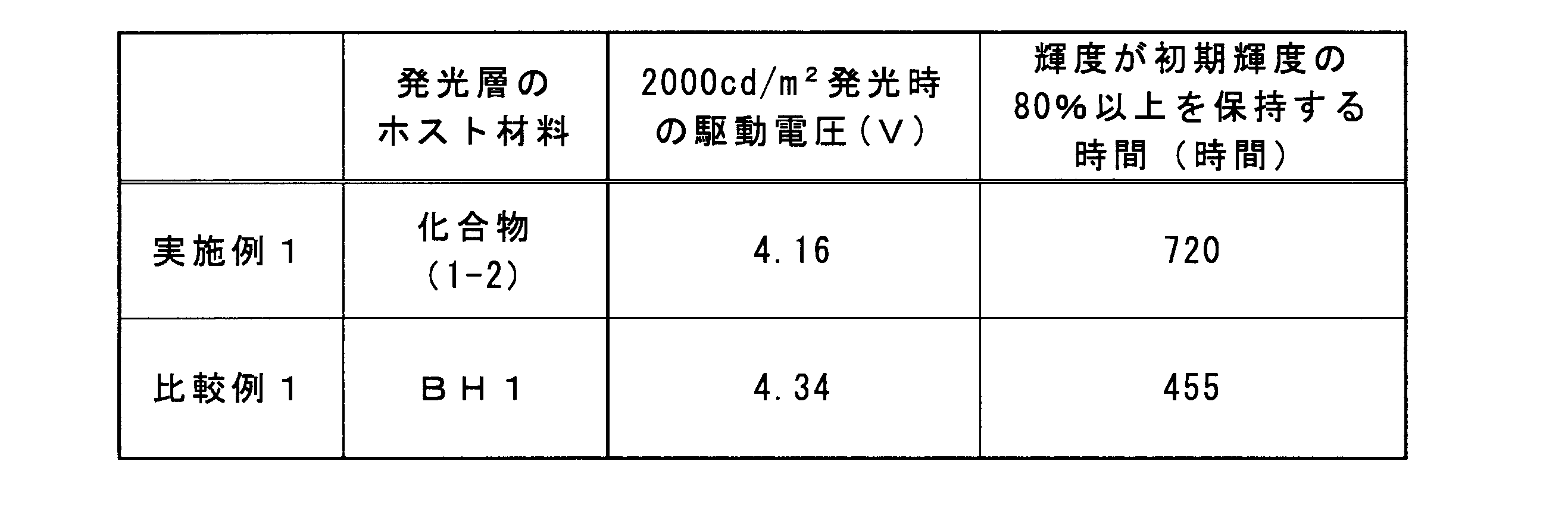
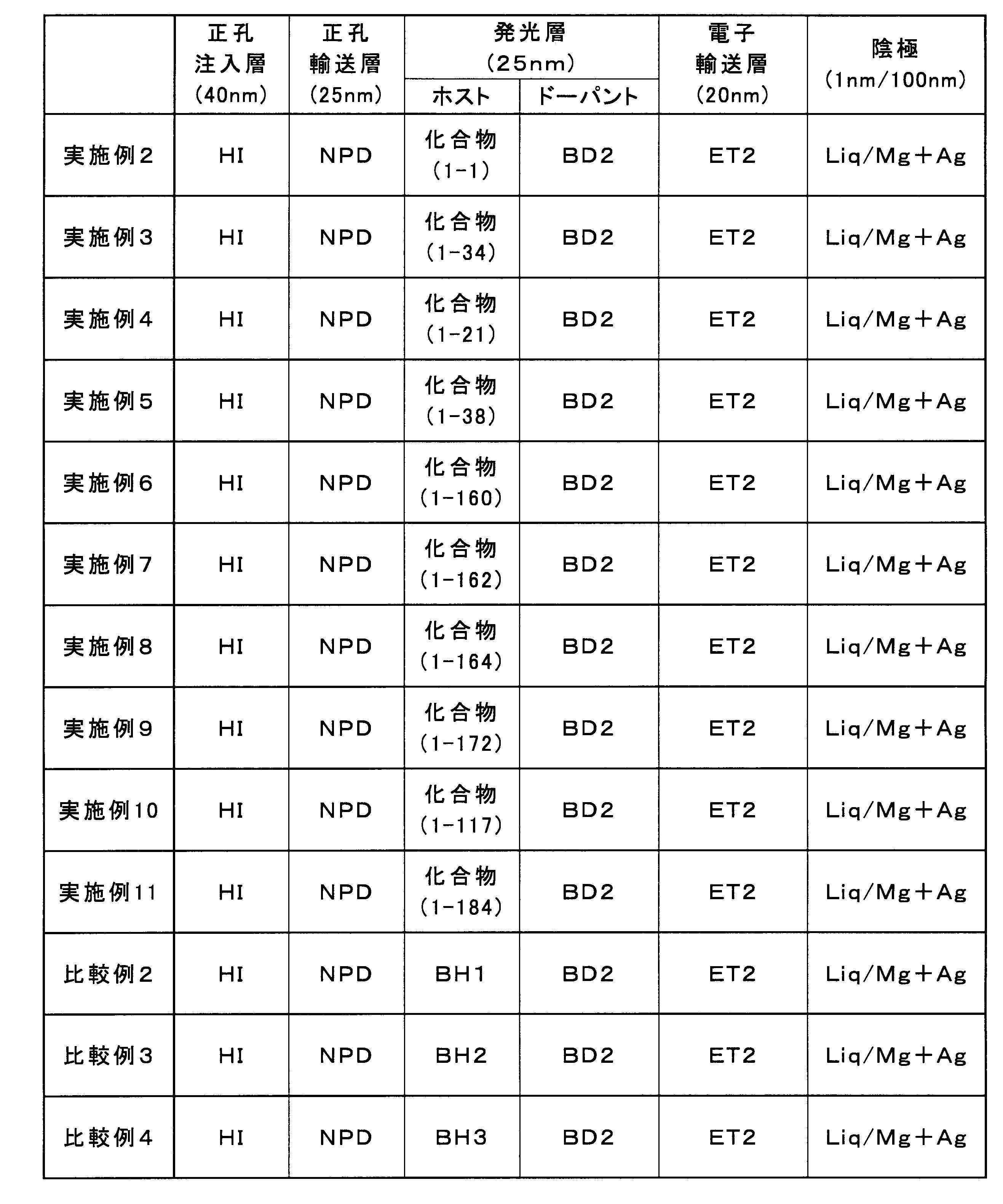
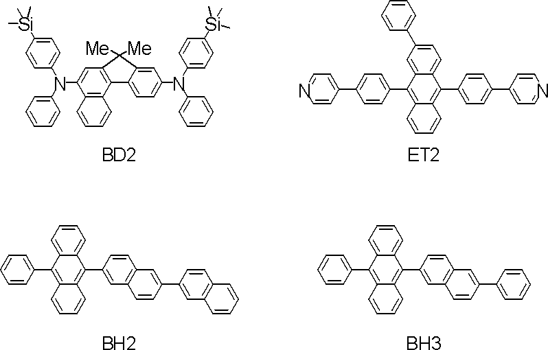
<化合物(1-1)を発光層のホスト材料に用いた素子>
スパッタリングにより180nmの厚さに製膜したITOを150nmまで研磨した、26mm×28mm×0.7mmのガラス基板((株)オプトサイエンス製)を透明支持基板とした。この透明支持基板を市販の蒸着装置(昭和真空(株)製)の基板ホルダーに固定し、HIを入れたモリブデン製蒸着用ボート、NPDを入れたモリブデン製蒸着用ボート、化合物(1-1)を入れたモリブデン製蒸着用ボート、BD2を入れたモリブデン製蒸着用ボート、ET2を入れたモリブデン製蒸着用ボート、Liqを入れたモリブデン製蒸着用ボート、マグネシウムを入れたモリブデンボートおよび銀を入れたタングステン製蒸着用ボートを装着した。
発光層のホスト材料である化合物(1-1)を化合物(1-34)に替えた以外は実施例2に準じた方法で有機EL素子を得た。ITO電極を陽極、Liq/アルミニウム電極を陰極として、初期輝度2000cd/m2を得るための電流密度により、定電流駆動試験を実施したところ、駆動試験開始電圧は3.93Vで初期輝度の80%(1600cd/m2)以上の輝度を保持する時間は276時間であった。
発光層のホスト材料である化合物(1-1)を化合物(1-21)に替えた以外は実施例2に準じた方法で有機EL素子を得た。ITO電極を陽極、Liq/アルミニウム電極を陰極として、初期輝度2000cd/m2を得るための電流密度により、定電流駆動試験を実施したところ、駆動試験開始電圧は4.03Vで初期輝度の80%(1600cd/m2)以上の輝度を保持する時間は265時間であった。
発光層のホスト材料である化合物(1-1)を化合物(1-38)に替えた以外は実施例2に準じた方法で有機EL素子を得た。ITO電極を陽極、Liq/アルミニウム電極を陰極として、初期輝度2000cd/m2を得るための電流密度により、定電流駆動試験を実施したところ、駆動試験開始電圧は3.70Vで初期輝度の80%(1600cd/m2)以上の輝度を保持する時間は235時間であった。
発光層のホスト材料である化合物(1-1)を化合物(1-160)に替えた以外は実施例2に準じた方法で有機EL素子を得た。ITO電極を陽極、Liq/アルミニウム電極を陰極として、初期輝度2000cd/m2を得るための電流密度により、定電流駆動試験を実施したところ、駆動試験開始電圧は3.98Vで初期輝度の80%(1600cd/m2)以上の輝度を保持する時間は228時間であった。
発光層のホスト材料である化合物(1-1)を化合物(1-162)に替えた以外は実施例2に準じた方法で有機EL素子を得た。ITO電極を陽極、Liq/アルミニウム電極を陰極として、初期輝度2000cd/m2を得るための電流密度により、定電流駆動試験を実施したところ、駆動試験開始電圧は4.15Vで初期輝度の80%(1600cd/m2)以上の輝度を保持する時間は263時間であった。
発光層のホスト材料である化合物(1-1)を化合物(1-164)に替えた以外は実施例2に準じた方法で有機EL素子を得た。ITO電極を陽極、Liq/アルミニウム電極を陰極として、初期輝度2000cd/m2を得るための電流密度により、定電流駆動試験を実施したところ、駆動試験開始電圧は3.67Vで初期輝度の80%(1600cd/m2)以上の輝度を保持する時間は271時間であった。
発光層のホスト材料である化合物(1-1)を化合物(1-172)に替えた以外は実施例2に準じた方法で有機EL素子を得た。ITO電極を陽極、Liq/アルミニウム電極を陰極として、初期輝度2000cd/m2を得るための電流密度により、定電流駆動試験を実施したところ、駆動試験開始電圧は3.82Vで初期輝度の80%(1600cd/m2)以上の輝度を保持する時間は261時間であった。
発光層のホスト材料である化合物(1-1)を化合物(1-117)に替えた以外は実施例2に準じた方法で有機EL素子を得た。ITO電極を陽極、Liq/アルミニウム電極を陰極として、初期輝度2000cd/m2を得るための電流密度により、定電流駆動試験を実施したところ、駆動試験開始電圧は4.30Vで初期輝度の80%(1600cd/m2)以上の輝度を保持する時間は275時間であった。
発光層のホスト材料である化合物(1-1)を化合物(1-184)に替えた以外は実施例2に準じた方法で有機EL素子を得た。ITO電極を陽極、Liq/アルミニウム電極を陰極として、初期輝度2000cd/m2を得るための電流密度により、定電流駆動試験を実施したところ、駆動試験開始電圧は4.21Vで初期輝度の80%(1600cd/m2)以上の輝度を保持する時間は231時間であった。
発光層のホスト材料である化合物(1-1)をBH1に替えた以外は実施例2に準じた方法で有機EL素子を得た。ITO電極を陽極、Liq/アルミニウム電極を陰極として、初期輝度2000cd/m2を得るための電流密度により、定電流駆動試験を実施したところ、駆動試験開始電圧は4.78Vで初期輝度の80%(1600cd/m2)以上の輝度を保持する時間は178時間であった。
発光層のホスト材料である化合物(1-1)をBH2に替えた以外は実施例2に準じた方法で有機EL素子を得た。ITO電極を陽極、Liq/アルミニウム電極を陰極として、初期輝度2000cd/m2を得るための電流密度により、定電流駆動試験を実施したところ、駆動試験開始電圧は4.35Vで初期輝度の80%(1600cd/m2)以上の輝度を保持する時間は189時間であった。
発光層のホスト材料である化合物(1-1)をBH3に替えた以外は実施例2に準じた方法で有機EL素子を得た。ITO電極を陽極、Liq/アルミニウム電極を陰極として、初期輝度2000cd/m2を得るための電流密度により、定電流駆動試験を実施したところ、駆動試験開始電圧は4.64Vで初期輝度の80%(1600cd/m2)以上の輝度を保持する時間は171時間であった。
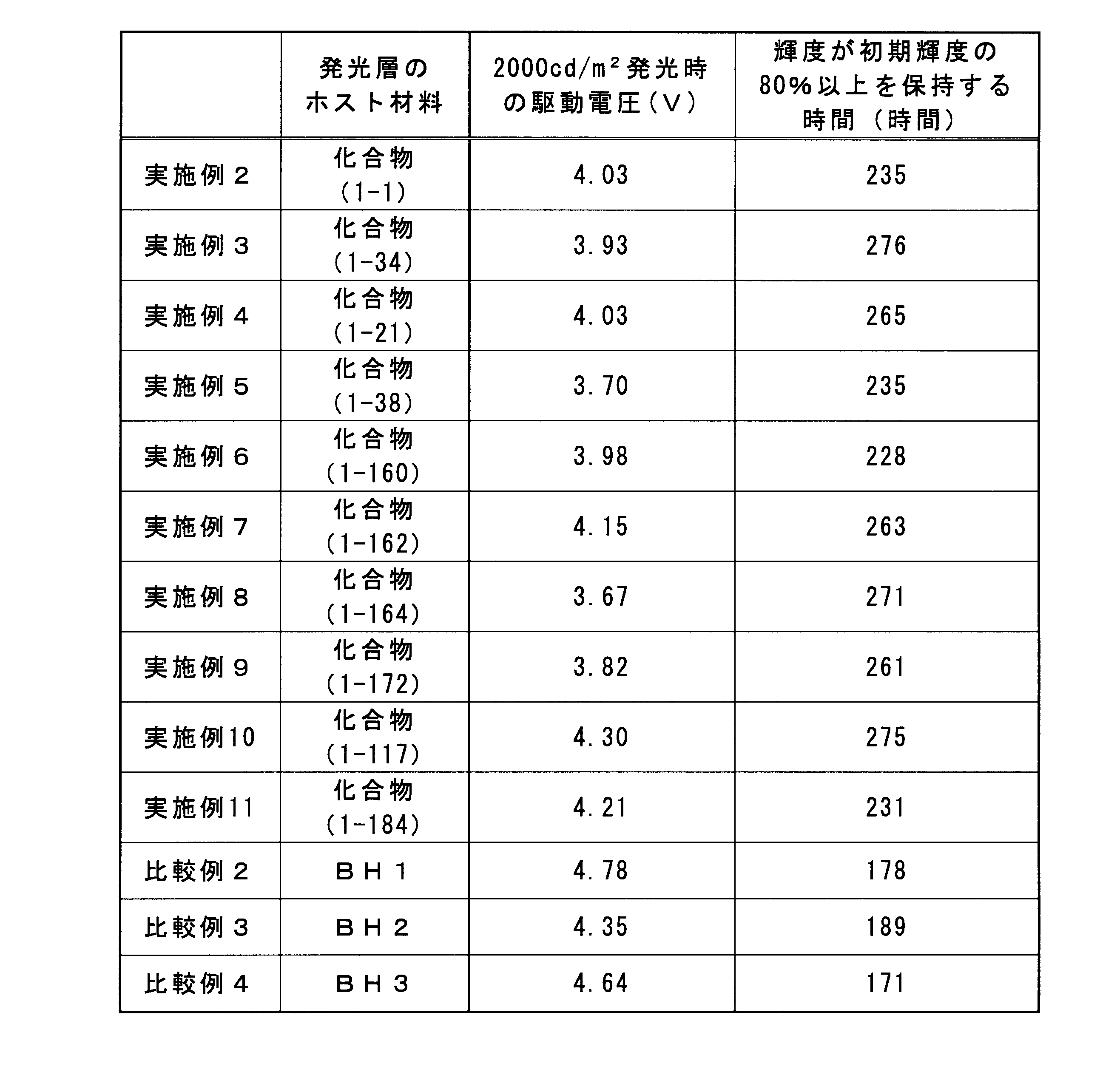
101 基板
102 陽極
103 正孔注入層
104 正孔輸送層
105 発光層
106 電子輸送層
107 電子注入層
108 陰極
Claims (14)
- 下記一般式(1)で表される化合物。
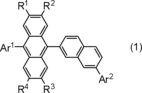
式(1)中、
Ar1は、置換されていてもよい、炭素数10~30のアリールであり、
Ar2は、置換されていてもよい、炭素数6~30のアリールであり、
R1~R4は、それぞれ独立して、水素または炭素数1~4のアルキルであり、そして、
式(1)で表される化合物における少なくとも1つの水素が重水素で置換されていてもよい。 - Ar1は、ナフチル、ビフェニリル、ビナフチル、テルフェニリル、クアテルフェニリル、ナフチルフェニル、フェニルナフチル、フェナントリル、フェナントリルフェニル、クリセニル、ピレニルフェニルまたはトリフェニレニルであり、これらは炭素数1~12のアルキルまたは炭素数3~12のシクロアルキルで置換されていてもよく、
Ar2は、フェニル、ナフチル、ビフェニリル、ビナフチル、テルフェニリル、クアテルフェニリル、ナフチルフェニル、フェニルナフチル、フェナントリル、フェナントリルフェニル、クリセニル、ピレニルフェニルまたはトリフェニレニルであり、これらは炭素数1~12のアルキルまたは炭素数3~12のシクロアルキルで置換されていてもよく、
R1~R4は、それぞれ独立して、水素、メチル、イソプロピルまたはt-ブチルであり、そして、
式(1)で表される化合物における少なくとも1つの水素が重水素で置換されていてもよい、
請求項1に記載の化合物。 - Ar1は、1-ナフチル、2-ナフチル、2-ビフェニリル、3-ビフェニリル、4-ビフェニリル、4-フェニル-1-ナフチル、m-テルフェニル-5’-イル、フェナントレン-9-イルまたはトリフェニレン-2-イルであり、
Ar2は、フェニル、1-ナフチル、2-ナフチル、2-ビフェニリル、3-ビフェニリル、4-ビフェニリル、m-テルフェニル-5’-イル、4-(ナフタレン-1-イル)フェニル、4-(ナフタレン-2-イル)フェニル、フェナントレン-9-イルまたはトリフェニレン-2-イルであり、
R1~R4は、水素であり、そして、
式(1)で表される化合物における少なくとも1つの水素が重水素で置換されていてもよい、
請求項1または2に記載の化合物。 - Ar1は、1-ナフチル、2-ビフェニリル、3-ビフェニリル、4-ビフェニリル、4-フェニル-1-ナフチル、m-テルフェニル-5’-イル、フェナントレン-9-イルまたはトリフェニレン-2-イルであり、そして、
Ar2における少なくとも1つの水素が重水素で置換されていてもよい、
請求項3に記載の化合物。 - 下記式(1-2)で表される化合物。

- 下記式(1-1)、式(1-21)、式(1-34)、式(1-38)、式(1-117)または式(1-129)で表される化合物。
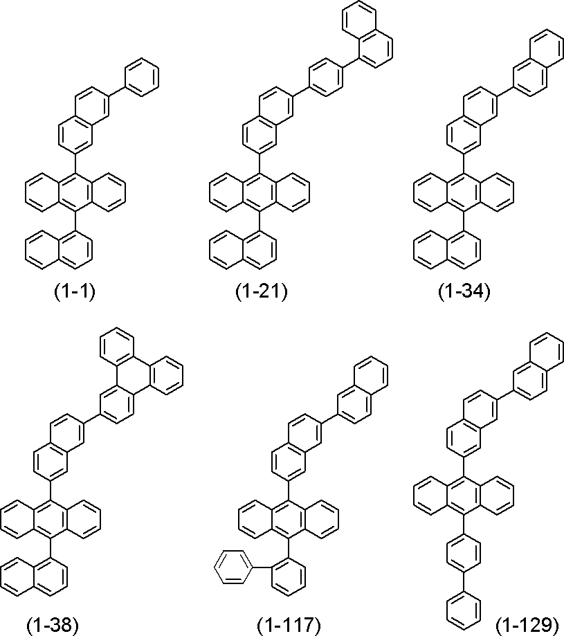
- 下記式(1-160)、式(1-162)、式(1-164)、式(1-166)、式(1-172)または式(1-184)で表される化合物。
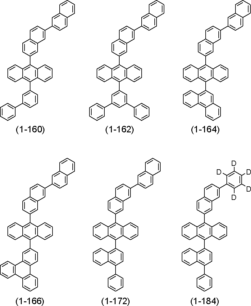
- 請求項1~7のいずれかに記載の化合物で表される発光層用材料。
- 陽極および陰極からなる一対の電極と、該一対の電極間に配置され、請求項8に記載する発光層用材料を含有する発光層とを有する、有機電界発光素子。
- 前記発光層に、スチルベン構造を有するアミン、芳香族アミン誘導体およびクマリン誘導体からなる群から選択される少なくとも1つを含有する、請求項9に記載する有機電界発光素子。
- さらに、前記陰極と前記発光層との間に配置された電子輸送層および/または電子注入層を有し、該電子輸送層および電子注入層の少なくとも1つは、キノリノール系金属錯体、ピリジン誘導体、フェナントロリン誘導体、ボラン誘導体およびベンゾイミダゾール誘導体からなる群から選択される少なくとも1つを含有する、請求項9または10に記載する有機電界発光素子。
- 前記電子輸送層および電子注入層の少なくとも1つは、さらに、アルカリ金属、アルカリ土類金属、希土類金属、アルカリ金属の酸化物、アルカリ金属のハロゲン化物、アルカリ土類金属の酸化物、アルカリ土類金属のハロゲン化物、希土類金属の酸化物、希土類金属のハロゲン化物、アルカリ金属の有機錯体、アルカリ土類金属の有機錯体および希土類金属の有機錯体からなる群から選択される少なくとも1つを含有する、請求項11に記載の有機電界発光素子。
- 請求項9~12のいずれかに記載する有機電界発光素子を備えた表示装置。
- 請求項9~12のいずれかに記載する有機電界発光素子を備えた照明装置。
Priority Applications (5)
| Application Number | Priority Date | Filing Date | Title |
|---|---|---|---|
| JP2012554831A JP5796582B2 (ja) | 2011-01-27 | 2012-01-26 | 新規アントラセン化合物およびこれを用いた有機電界発光素子 |
| US13/980,177 US9070885B2 (en) | 2011-01-27 | 2012-01-26 | Anthracene compound and organic electroluminescence element using same |
| KR1020137022465A KR101979037B1 (ko) | 2011-01-27 | 2012-01-26 | 신규 안트라센 화합물 및 이것을 이용한 유기 전계 발광 소자 |
| EP12739048.2A EP2669262B1 (en) | 2011-01-27 | 2012-01-26 | Novel anthracene compound and organic electroluminescence element using same |
| CN201280005620.3A CN103328420B (zh) | 2011-01-27 | 2012-01-26 | 蒽化合物及使用其的有机电激发光元件、发光层用材料、显示装置及照明装置 |
Applications Claiming Priority (2)
| Application Number | Priority Date | Filing Date | Title |
|---|---|---|---|
| JP2011015702 | 2011-01-27 | ||
| JP2011-015702 | 2011-07-08 |
Publications (1)
| Publication Number | Publication Date |
|---|---|
| WO2012102333A1 true WO2012102333A1 (ja) | 2012-08-02 |
Family
ID=46580897
Family Applications (1)
| Application Number | Title | Priority Date | Filing Date |
|---|---|---|---|
| PCT/JP2012/051640 Ceased WO2012102333A1 (ja) | 2011-01-27 | 2012-01-26 | 新規アントラセン化合物およびこれを用いた有機電界発光素子 |
Country Status (7)
| Country | Link |
|---|---|
| US (1) | US9070885B2 (ja) |
| EP (1) | EP2669262B1 (ja) |
| JP (1) | JP5796582B2 (ja) |
| KR (1) | KR101979037B1 (ja) |
| CN (1) | CN103328420B (ja) |
| TW (1) | TWI526518B (ja) |
| WO (1) | WO2012102333A1 (ja) |
Cited By (8)
| Publication number | Priority date | Publication date | Assignee | Title |
|---|---|---|---|---|
| JP2015065325A (ja) * | 2013-09-25 | 2015-04-09 | 出光興産株式会社 | 有機エレクトロルミネッセンス素子、および電子機器 |
| JP2015065323A (ja) * | 2013-09-25 | 2015-04-09 | 出光興産株式会社 | 有機エレクトロルミネッセンス素子、および電子機器 |
| JP2016108297A (ja) * | 2014-12-09 | 2016-06-20 | 旭有機材工業株式会社 | アントラセン誘導体、その製造方法、フェノール樹脂、フォトレジスト用組成物及び発光剤 |
| JP2016127083A (ja) * | 2014-12-26 | 2016-07-11 | 出光興産株式会社 | 有機エレクトロルミネッセンス素子用材料、有機エレクトロルミネッセンス素子及び電子機器 |
| KR20170126888A (ko) | 2015-03-09 | 2017-11-20 | 가꼬우 호징 관세이 가쿠잉 | 다환 방향족 화합물 및 발광층 형성용 조성물 |
| KR20170130435A (ko) | 2015-03-25 | 2017-11-28 | 가꼬우 호징 관세이 가쿠잉 | 다환 방향족 화합물 및 발광층 형성용 조성물 |
| WO2018212169A1 (ja) | 2017-05-16 | 2018-11-22 | 学校法人関西学院 | 多環芳香族化合物 |
| JP2020113781A (ja) * | 2015-03-24 | 2020-07-27 | 学校法人関西学院 | 有機電界発光素子 |
Families Citing this family (16)
| Publication number | Priority date | Publication date | Assignee | Title |
|---|---|---|---|---|
| JPWO2014083786A1 (ja) * | 2012-11-30 | 2017-01-05 | パナソニックIpマネジメント株式会社 | 有機エレクトロルミネッセンス素子及び照明装置 |
| US9231217B2 (en) | 2013-11-28 | 2016-01-05 | Semiconductor Energy Laboratory Co., Ltd. | Synthesis method of organometallic complex, synthesis method of pyrazine derivative, 5,6-diaryl-2-pyrazyl triflate, light-emitting element, light-emitting device, electronic device, and lighting device |
| WO2016076629A1 (en) * | 2014-11-11 | 2016-05-19 | Rohm And Haas Electronic Materials Korea Ltd. | A plurality of host materials and an organic electroluminescence device comprising the same |
| US10381569B2 (en) * | 2014-11-25 | 2019-08-13 | Universal Display Corporation | Organic electroluminescent materials and devices |
| KR102338908B1 (ko) | 2015-03-03 | 2021-12-14 | 삼성디스플레이 주식회사 | 유기 발광 소자 |
| US10700284B2 (en) * | 2015-07-20 | 2020-06-30 | Lg Chem, Ltd. | Photoactive composition |
| KR102599157B1 (ko) * | 2015-08-14 | 2023-11-06 | 메르크 파텐트 게엠베하 | 유기 전계발광 소자용 페녹사진 유도체 |
| KR102591635B1 (ko) | 2015-10-27 | 2023-10-20 | 삼성디스플레이 주식회사 | 유기 발광 소자 |
| US10886491B2 (en) * | 2015-11-10 | 2021-01-05 | Novaled Gmbh | Process for making a metal containing layer |
| KR102574052B1 (ko) | 2015-11-19 | 2023-09-04 | 엘지디스플레이 주식회사 | 유기발광 표시장치 |
| US10374183B2 (en) | 2015-11-19 | 2019-08-06 | Lg Display Co., Ltd. | Organic light emitting display device having layer to control charge transfer |
| KR102399570B1 (ko) | 2015-11-26 | 2022-05-19 | 삼성디스플레이 주식회사 | 유기 발광 소자 |
| US11910707B2 (en) | 2015-12-23 | 2024-02-20 | Samsung Display Co., Ltd. | Organic light-emitting device |
| KR20170127101A (ko) | 2016-05-10 | 2017-11-21 | 삼성디스플레이 주식회사 | 유기 발광 소자 |
| EP3738965B1 (en) * | 2019-05-08 | 2023-10-04 | Samsung Display Co., Ltd. | Organic molecules for optoelectronic devices |
| TWI835062B (zh) * | 2021-02-04 | 2024-03-11 | 南韓商Lg化學股份有限公司 | 氘代蒽化合物的製備方法、反應組成物、氘代蒽化合物以及組成物 |
Citations (44)
| Publication number | Priority date | Publication date | Assignee | Title |
|---|---|---|---|---|
| JPH01245087A (ja) | 1987-12-11 | 1989-09-29 | Idemitsu Kosan Co Ltd | 有機エレクトロルミネッセンス素子 |
| JPH02247278A (ja) | 1989-03-20 | 1990-10-03 | Idemitsu Kosan Co Ltd | エレクトロルミネッセンス素子 |
| JPH06298758A (ja) | 1993-04-16 | 1994-10-25 | Chisso Corp | クマリン誘導体 |
| JPH10335066A (ja) | 1997-06-02 | 1998-12-18 | Sony Corp | 有機電界発光素子およびこれを用いたフラットパネルディスプレイ |
| JPH1197178A (ja) | 1997-09-24 | 1999-04-09 | Mitsui Chem Inc | 有機電界発光素子 |
| JP2000026324A (ja) | 1998-07-02 | 2000-01-25 | Mitsui Chemicals Inc | 炭化水素化合物および有機電界発光素子 |
| JP2000034234A (ja) | 1998-07-15 | 2000-02-02 | Mitsui Chemicals Inc | 炭化水素化合物および有機電界発光素子 |
| JP2000133457A (ja) | 1998-10-30 | 2000-05-12 | Mitsui Chemicals Inc | 炭化水素化合物および有機電界発光素子 |
| WO2000040586A1 (en) | 1999-01-08 | 2000-07-13 | Chisso Corporation | Borane derivatives and organic electroluminescents |
| JP2001052869A (ja) | 1999-08-11 | 2001-02-23 | Hayashibara Biochem Lab Inc | 有機電界発光素子 |
| JP2001076876A (ja) | 1999-09-01 | 2001-03-23 | Hayashibara Biochem Lab Inc | 有機電界発光素子 |
| JP2001081090A (ja) | 1999-03-09 | 2001-03-27 | Hayashibara Biochem Lab Inc | ピラン誘導体 |
| JP2001217077A (ja) | 2000-02-01 | 2001-08-10 | Mitsui Chemicals Inc | 有機電界発光素子 |
| JP2001220577A (ja) | 1999-03-09 | 2001-08-14 | Hayashibara Biochem Lab Inc | ピラン誘導体 |
| JP2001267079A (ja) | 2000-03-23 | 2001-09-28 | Mitsui Chemicals Inc | 炭化水素化合物および有機電界発光素子 |
| JP2001267078A (ja) | 2000-03-23 | 2001-09-28 | Mitsui Chemicals Inc | 炭化水素化合物および有機電界発光素子 |
| JP2001267076A (ja) | 2000-03-16 | 2001-09-28 | Mitsui Chemicals Inc | 炭化水素化合物および有機電界発光素子 |
| JP2001267075A (ja) | 2000-03-16 | 2001-09-28 | Mitsui Chemicals Inc | 炭化水素化合物および有機電界発光素子 |
| JP2001307884A (ja) | 2000-04-26 | 2001-11-02 | Toray Ind Inc | 発光素子 |
| JP2002234892A (ja) | 2000-11-07 | 2002-08-23 | Hayashibara Biochem Lab Inc | ピラン誘導体 |
| JP2003257621A (ja) | 2002-02-27 | 2003-09-12 | Seiko Epson Corp | 有機el素子とその製造方法ならびに表示装置 |
| JP2003277741A (ja) | 2002-03-26 | 2003-10-02 | Sharp Corp | 有機el発光素子およびそれを用いた液晶表示装置 |
| JP2003321546A (ja) | 2002-04-26 | 2003-11-14 | Nippon Hoso Kyokai <Nhk> | 燐光発光性高分子化合物ならびにこれを用いた発光材料および有機el素子 |
| JP2003347056A (ja) | 2002-05-30 | 2003-12-05 | Fuji Photo Film Co Ltd | 発光素子 |
| JP2004006222A (ja) | 2002-04-22 | 2004-01-08 | Hayashibara Biochem Lab Inc | 有機電界発光素子 |
| JP2004043646A (ja) | 2002-07-11 | 2004-02-12 | Hayashibara Biochem Lab Inc | 有機電界発光素子 |
| JP2004119211A (ja) | 2002-09-26 | 2004-04-15 | Toyota Industries Corp | El素子用透明基板及びel装置並びに液晶表示装置 |
| JP2004281086A (ja) | 2003-03-12 | 2004-10-07 | Nippon Hoso Kyokai <Nhk> | フレキシブルフルカラー有機elディスプレイおよびその製造方法 |
| JP2005097283A (ja) | 2003-08-29 | 2005-04-14 | Semiconductor Energy Lab Co Ltd | ピラン誘導体とその製造方法、並びにピラン誘導体を用いた発光素子及び発光装置。 |
| JP2005126399A (ja) | 2003-10-27 | 2005-05-19 | Semiconductor Energy Lab Co Ltd | ピラン誘導体 |
| JP2005139390A (ja) | 2003-11-10 | 2005-06-02 | Sony Corp | 含クマリン発光性有機材料及び有機el素子 |
| JP2005167175A (ja) | 2003-12-04 | 2005-06-23 | Novaled Gmbh | 有機半導体をキノンジイミン誘導体によってドーピングする方法 |
| JP2006156888A (ja) | 2004-12-01 | 2006-06-15 | Idemitsu Kosan Co Ltd | 有機電界発光素子 |
| JP2007027587A (ja) | 2005-07-20 | 2007-02-01 | Chisso Corp | 有機電界発光素子 |
| JP2009033146A (ja) * | 2007-06-28 | 2009-02-12 | Mitsubishi Chemicals Corp | 湿式成膜用電荷輸送材料、湿式成膜法用電荷輸送材料組成物、有機電界発光素子、および有機elディスプレイ |
| KR20090052774A (ko) * | 2007-11-21 | 2009-05-26 | 주식회사 엘지화학 | 신규한 안트라센 유도체 및 이를 이용한 유기전기소자 |
| JP2009177128A (ja) * | 2008-01-28 | 2009-08-06 | Samsung Mobile Display Co Ltd | 有機電界発光素子及びその製造方法 |
| US20090206740A1 (en) * | 2008-01-28 | 2009-08-20 | Samsung Mobile Display Co., Ltd. | Organic light emitting diode and method of fabricating the same |
| US20090230855A1 (en) * | 2008-03-14 | 2009-09-17 | Myeong-Suk Kim | Novel organic compound and organic light emitting device comprising the same |
| KR20090107209A (ko) * | 2008-04-08 | 2009-10-13 | 동우 화인켐 주식회사 | 비대칭 나프탈레닐카바졸 유도체, 이를 이용하는유기전기발광소자용 유기박막재료 및 유기전기발광소자 |
| WO2010099534A2 (en) * | 2009-02-27 | 2010-09-02 | E. I. Du Pont De Nemours And Company | Deuterated compounds for electronic applications |
| WO2010114256A2 (en) * | 2009-03-31 | 2010-10-07 | Dow Advanced Display Materials,Ltd. | Novel organic electroluminescent compounds and organic electroluminescent device using the same |
| WO2010137678A1 (ja) * | 2009-05-29 | 2010-12-02 | チッソ株式会社 | 電子輸送材料およびこれを用いた有機電界発光素子 |
| KR20110076376A (ko) * | 2009-12-29 | 2011-07-06 | 에스에프씨 주식회사 | 호스트 화합물 및 이를 이용한 유기전계발광소자 |
Family Cites Families (11)
| Publication number | Priority date | Publication date | Assignee | Title |
|---|---|---|---|---|
| US7514158B2 (en) | 2001-12-13 | 2009-04-07 | Kabushiki Kaisha Hayashibara Seibutsu Kagaku Kenkyujo | Coumarin compound |
| CN1914293B (zh) | 2003-12-19 | 2010-12-01 | 出光兴产株式会社 | 有机电致发光器件用发光材料、使用该材料的有机电致发光器件以及有机电致发光器件用材料 |
| KR20060134979A (ko) | 2004-03-19 | 2006-12-28 | 칫소가부시키가이샤 | 유기 전계 발광 소자 |
| JP4788202B2 (ja) | 2004-07-09 | 2011-10-05 | Jnc株式会社 | 発光材料およびこれを用いた有機電界発光素子 |
| JP4900670B2 (ja) | 2006-05-01 | 2012-03-21 | Jnc株式会社 | 有機電界発光素子 |
| JPWO2008105471A1 (ja) | 2007-02-28 | 2010-06-03 | 出光興産株式会社 | 有機el材料含有溶液、有機el薄膜形成方法および有機el素子 |
| KR101068224B1 (ko) * | 2008-02-05 | 2011-09-28 | 에스에프씨 주식회사 | 안트라센 유도체 및 이를 포함하는 유기전계발광소자 |
| WO2010032447A1 (ja) | 2008-09-19 | 2010-03-25 | 出光興産株式会社 | 有機エレクトロルミネッセンス材料組成物、薄膜形成方法及び有機エレクトロルミネッセンス素子 |
| WO2010035723A1 (ja) | 2008-09-24 | 2010-04-01 | 保土谷化学工業株式会社 | 置換されたアントラセン環構造とピリドインドール環構造を有する化合物および有機エレクトロルミネッセンス素子 |
| WO2010052885A1 (ja) | 2008-11-06 | 2010-05-14 | 出光興産株式会社 | 有機エレクトロルミネッセンス素子 |
| JP5713699B2 (ja) | 2011-01-20 | 2015-05-07 | キヤノン株式会社 | 有機化合物、有機発光素子及び画像表示装置 |
-
2012
- 2012-01-26 KR KR1020137022465A patent/KR101979037B1/ko active Active
- 2012-01-26 EP EP12739048.2A patent/EP2669262B1/en not_active Not-in-force
- 2012-01-26 US US13/980,177 patent/US9070885B2/en not_active Expired - Fee Related
- 2012-01-26 CN CN201280005620.3A patent/CN103328420B/zh active Active
- 2012-01-26 JP JP2012554831A patent/JP5796582B2/ja active Active
- 2012-01-26 WO PCT/JP2012/051640 patent/WO2012102333A1/ja not_active Ceased
- 2012-01-30 TW TW101102889A patent/TWI526518B/zh not_active IP Right Cessation
Patent Citations (44)
| Publication number | Priority date | Publication date | Assignee | Title |
|---|---|---|---|---|
| JPH01245087A (ja) | 1987-12-11 | 1989-09-29 | Idemitsu Kosan Co Ltd | 有機エレクトロルミネッセンス素子 |
| JPH02247278A (ja) | 1989-03-20 | 1990-10-03 | Idemitsu Kosan Co Ltd | エレクトロルミネッセンス素子 |
| JPH06298758A (ja) | 1993-04-16 | 1994-10-25 | Chisso Corp | クマリン誘導体 |
| JPH10335066A (ja) | 1997-06-02 | 1998-12-18 | Sony Corp | 有機電界発光素子およびこれを用いたフラットパネルディスプレイ |
| JPH1197178A (ja) | 1997-09-24 | 1999-04-09 | Mitsui Chem Inc | 有機電界発光素子 |
| JP2000026324A (ja) | 1998-07-02 | 2000-01-25 | Mitsui Chemicals Inc | 炭化水素化合物および有機電界発光素子 |
| JP2000034234A (ja) | 1998-07-15 | 2000-02-02 | Mitsui Chemicals Inc | 炭化水素化合物および有機電界発光素子 |
| JP2000133457A (ja) | 1998-10-30 | 2000-05-12 | Mitsui Chemicals Inc | 炭化水素化合物および有機電界発光素子 |
| WO2000040586A1 (en) | 1999-01-08 | 2000-07-13 | Chisso Corporation | Borane derivatives and organic electroluminescents |
| JP2001220577A (ja) | 1999-03-09 | 2001-08-14 | Hayashibara Biochem Lab Inc | ピラン誘導体 |
| JP2001081090A (ja) | 1999-03-09 | 2001-03-27 | Hayashibara Biochem Lab Inc | ピラン誘導体 |
| JP2001052869A (ja) | 1999-08-11 | 2001-02-23 | Hayashibara Biochem Lab Inc | 有機電界発光素子 |
| JP2001076876A (ja) | 1999-09-01 | 2001-03-23 | Hayashibara Biochem Lab Inc | 有機電界発光素子 |
| JP2001217077A (ja) | 2000-02-01 | 2001-08-10 | Mitsui Chemicals Inc | 有機電界発光素子 |
| JP2001267076A (ja) | 2000-03-16 | 2001-09-28 | Mitsui Chemicals Inc | 炭化水素化合物および有機電界発光素子 |
| JP2001267075A (ja) | 2000-03-16 | 2001-09-28 | Mitsui Chemicals Inc | 炭化水素化合物および有機電界発光素子 |
| JP2001267079A (ja) | 2000-03-23 | 2001-09-28 | Mitsui Chemicals Inc | 炭化水素化合物および有機電界発光素子 |
| JP2001267078A (ja) | 2000-03-23 | 2001-09-28 | Mitsui Chemicals Inc | 炭化水素化合物および有機電界発光素子 |
| JP2001307884A (ja) | 2000-04-26 | 2001-11-02 | Toray Ind Inc | 発光素子 |
| JP2002234892A (ja) | 2000-11-07 | 2002-08-23 | Hayashibara Biochem Lab Inc | ピラン誘導体 |
| JP2003257621A (ja) | 2002-02-27 | 2003-09-12 | Seiko Epson Corp | 有機el素子とその製造方法ならびに表示装置 |
| JP2003277741A (ja) | 2002-03-26 | 2003-10-02 | Sharp Corp | 有機el発光素子およびそれを用いた液晶表示装置 |
| JP2004006222A (ja) | 2002-04-22 | 2004-01-08 | Hayashibara Biochem Lab Inc | 有機電界発光素子 |
| JP2003321546A (ja) | 2002-04-26 | 2003-11-14 | Nippon Hoso Kyokai <Nhk> | 燐光発光性高分子化合物ならびにこれを用いた発光材料および有機el素子 |
| JP2003347056A (ja) | 2002-05-30 | 2003-12-05 | Fuji Photo Film Co Ltd | 発光素子 |
| JP2004043646A (ja) | 2002-07-11 | 2004-02-12 | Hayashibara Biochem Lab Inc | 有機電界発光素子 |
| JP2004119211A (ja) | 2002-09-26 | 2004-04-15 | Toyota Industries Corp | El素子用透明基板及びel装置並びに液晶表示装置 |
| JP2004281086A (ja) | 2003-03-12 | 2004-10-07 | Nippon Hoso Kyokai <Nhk> | フレキシブルフルカラー有機elディスプレイおよびその製造方法 |
| JP2005097283A (ja) | 2003-08-29 | 2005-04-14 | Semiconductor Energy Lab Co Ltd | ピラン誘導体とその製造方法、並びにピラン誘導体を用いた発光素子及び発光装置。 |
| JP2005126399A (ja) | 2003-10-27 | 2005-05-19 | Semiconductor Energy Lab Co Ltd | ピラン誘導体 |
| JP2005139390A (ja) | 2003-11-10 | 2005-06-02 | Sony Corp | 含クマリン発光性有機材料及び有機el素子 |
| JP2005167175A (ja) | 2003-12-04 | 2005-06-23 | Novaled Gmbh | 有機半導体をキノンジイミン誘導体によってドーピングする方法 |
| JP2006156888A (ja) | 2004-12-01 | 2006-06-15 | Idemitsu Kosan Co Ltd | 有機電界発光素子 |
| JP2007027587A (ja) | 2005-07-20 | 2007-02-01 | Chisso Corp | 有機電界発光素子 |
| JP2009033146A (ja) * | 2007-06-28 | 2009-02-12 | Mitsubishi Chemicals Corp | 湿式成膜用電荷輸送材料、湿式成膜法用電荷輸送材料組成物、有機電界発光素子、および有機elディスプレイ |
| KR20090052774A (ko) * | 2007-11-21 | 2009-05-26 | 주식회사 엘지화학 | 신규한 안트라센 유도체 및 이를 이용한 유기전기소자 |
| JP2009177128A (ja) * | 2008-01-28 | 2009-08-06 | Samsung Mobile Display Co Ltd | 有機電界発光素子及びその製造方法 |
| US20090206740A1 (en) * | 2008-01-28 | 2009-08-20 | Samsung Mobile Display Co., Ltd. | Organic light emitting diode and method of fabricating the same |
| US20090230855A1 (en) * | 2008-03-14 | 2009-09-17 | Myeong-Suk Kim | Novel organic compound and organic light emitting device comprising the same |
| KR20090107209A (ko) * | 2008-04-08 | 2009-10-13 | 동우 화인켐 주식회사 | 비대칭 나프탈레닐카바졸 유도체, 이를 이용하는유기전기발광소자용 유기박막재료 및 유기전기발광소자 |
| WO2010099534A2 (en) * | 2009-02-27 | 2010-09-02 | E. I. Du Pont De Nemours And Company | Deuterated compounds for electronic applications |
| WO2010114256A2 (en) * | 2009-03-31 | 2010-10-07 | Dow Advanced Display Materials,Ltd. | Novel organic electroluminescent compounds and organic electroluminescent device using the same |
| WO2010137678A1 (ja) * | 2009-05-29 | 2010-12-02 | チッソ株式会社 | 電子輸送材料およびこれを用いた有機電界発光素子 |
| KR20110076376A (ko) * | 2009-12-29 | 2011-07-06 | 에스에프씨 주식회사 | 호스트 화합물 및 이를 이용한 유기전계발광소자 |
Non-Patent Citations (9)
| Title |
|---|
| APPL. PHYS. LETT., vol. 89, 2006, pages 252903 |
| APPL. PHYS. LETT., vol. 90, 2007, pages 123506 |
| APPL. PHYS. LETT., vol. 91, 2007, pages 083515 |
| APPL. PHYS. LETT., vol. 91, 2007, pages 251111 |
| CHEMICAL INDUSTRY DAILY, June 2004 (2004-06-01), pages 13 |
| J. BLOCHWITZ; M. PHEIFFER; T. FRITZ; K. LEO, APPL. PHYS. LETT., vol. 73, no. 6, 1998, pages 729 - 731 |
| M. PFEIFFER; A. BEYER; T. FRITZ; K. LEO, APPL. PHYS. LETT., vol. 73, no. 22, 1998, pages 3202 - 3204 |
| MATERIALS SCIENCE AND ENGINEERING: R: REPORTS, vol. 39, no. 5-6, 2002, pages 143 - 222 |
| See also references of EP2669262A4 |
Cited By (10)
| Publication number | Priority date | Publication date | Assignee | Title |
|---|---|---|---|---|
| JP2015065325A (ja) * | 2013-09-25 | 2015-04-09 | 出光興産株式会社 | 有機エレクトロルミネッセンス素子、および電子機器 |
| JP2015065323A (ja) * | 2013-09-25 | 2015-04-09 | 出光興産株式会社 | 有機エレクトロルミネッセンス素子、および電子機器 |
| JP2016108297A (ja) * | 2014-12-09 | 2016-06-20 | 旭有機材工業株式会社 | アントラセン誘導体、その製造方法、フェノール樹脂、フォトレジスト用組成物及び発光剤 |
| JP2016127083A (ja) * | 2014-12-26 | 2016-07-11 | 出光興産株式会社 | 有機エレクトロルミネッセンス素子用材料、有機エレクトロルミネッセンス素子及び電子機器 |
| KR20170126888A (ko) | 2015-03-09 | 2017-11-20 | 가꼬우 호징 관세이 가쿠잉 | 다환 방향족 화합물 및 발광층 형성용 조성물 |
| JP2020113781A (ja) * | 2015-03-24 | 2020-07-27 | 学校法人関西学院 | 有機電界発光素子 |
| KR20170130435A (ko) | 2015-03-25 | 2017-11-28 | 가꼬우 호징 관세이 가쿠잉 | 다환 방향족 화합물 및 발광층 형성용 조성물 |
| WO2018212169A1 (ja) | 2017-05-16 | 2018-11-22 | 学校法人関西学院 | 多環芳香族化合物 |
| KR20200006965A (ko) | 2017-05-16 | 2020-01-21 | 가꼬우 호징 관세이 가쿠잉 | 다환 방향족 화합물 |
| KR20240055908A (ko) | 2017-05-16 | 2024-04-29 | 가꼬우 호징 관세이 가쿠잉 | 다환 방향족 화합물 |
Also Published As
| Publication number | Publication date |
|---|---|
| US20130292665A1 (en) | 2013-11-07 |
| EP2669262A4 (en) | 2016-03-02 |
| CN103328420A (zh) | 2013-09-25 |
| EP2669262A1 (en) | 2013-12-04 |
| KR101979037B1 (ko) | 2019-05-15 |
| US9070885B2 (en) | 2015-06-30 |
| TW201233777A (en) | 2012-08-16 |
| CN103328420B (zh) | 2017-08-11 |
| JPWO2012102333A1 (ja) | 2014-06-30 |
| EP2669262B1 (en) | 2018-03-07 |
| KR20140006000A (ko) | 2014-01-15 |
| TWI526518B (zh) | 2016-03-21 |
| JP5796582B2 (ja) | 2015-10-21 |
Similar Documents
| Publication | Publication Date | Title |
|---|---|---|
| JP5796582B2 (ja) | 新規アントラセン化合物およびこれを用いた有機電界発光素子 | |
| KR102100309B1 (ko) | 발광층용 재료 및 이것을 사용한 유기 전계 발광 소자 | |
| JP5799637B2 (ja) | アントラセン誘導体およびこれを用いた有機電界発光素子 | |
| JP5982966B2 (ja) | ベンゾフルオレン化合物、該化合物を用いた発光層用材料および有機電界発光素子 | |
| TW201926760A (zh) | 有機元件用材料、有機電場發光元件、顯示裝置及照明裝置 | |
| JP6156389B2 (ja) | ベンゾフルオレン化合物、該化合物を用いた発光層用材料および有機電界発光素子 | |
| WO2013077141A1 (ja) | ベンゾフルオレン化合物、該化合物を用いた発光層用材料および有機電界発光素子 | |
| JP5949779B2 (ja) | ベンゾフルオレン化合物、該化合物を用いた発光層用材料および有機電界発光素子 | |
| JP6041058B2 (ja) | アントラセン系化合物、発光層用材料、これを用いた有機電界発光素子、表示装置および照明装置 | |
| JP5794155B2 (ja) | 新規な2,7−ビスアントリルナフタレン化合物およびこれを用いた有機電界発光素子 | |
| JP6341315B2 (ja) | 発光層用材料およびこれを用いた有機電界発光素子 | |
| JP2012094823A (ja) | ピリジルフェニル置換アントラセン化合物および有機電界発光素子 | |
| JP5776384B2 (ja) | ベンゾフルオレン化合物、該化合物を用いた発光層用材料および有機電界発光素子 | |
| JP5867269B2 (ja) | ベンゾフルオレン化合物、該化合物を用いた発光層用材料および有機電界発光素子 | |
| JP2017178832A (ja) | 自己組織化し得る多環式芳香族化合物およびそれを用いた有機el素子 |
Legal Events
| Date | Code | Title | Description |
|---|---|---|---|
| 121 | Ep: the epo has been informed by wipo that ep was designated in this application |
Ref document number: 12739048 Country of ref document: EP Kind code of ref document: A1 |
|
| ENP | Entry into the national phase |
Ref document number: 2012554831 Country of ref document: JP Kind code of ref document: A |
|
| WWE | Wipo information: entry into national phase |
Ref document number: 13980177 Country of ref document: US |
|
| WWE | Wipo information: entry into national phase |
Ref document number: 2012739048 Country of ref document: EP |
|
| NENP | Non-entry into the national phase |
Ref country code: DE |
|
| ENP | Entry into the national phase |
Ref document number: 20137022465 Country of ref document: KR Kind code of ref document: A |