WO2011114657A1 - スパッタリングターゲット及びその製造方法 - Google Patents
スパッタリングターゲット及びその製造方法 Download PDFInfo
- Publication number
- WO2011114657A1 WO2011114657A1 PCT/JP2011/001352 JP2011001352W WO2011114657A1 WO 2011114657 A1 WO2011114657 A1 WO 2011114657A1 JP 2011001352 W JP2011001352 W JP 2011001352W WO 2011114657 A1 WO2011114657 A1 WO 2011114657A1
- Authority
- WO
- WIPO (PCT)
- Prior art keywords
- sputtering target
- powder
- sputtering
- film
- manufacturing
- Prior art date
Links
- 238000005477 sputtering target Methods 0.000 title claims abstract description 93
- 238000004519 manufacturing process Methods 0.000 title claims abstract description 32
- 239000000843 powder Substances 0.000 claims abstract description 61
- 229910000807 Ga alloy Inorganic materials 0.000 claims abstract description 24
- 238000001513 hot isostatic pressing Methods 0.000 claims abstract description 18
- 229910052717 sulfur Inorganic materials 0.000 claims abstract description 14
- 229910052733 gallium Inorganic materials 0.000 claims abstract description 13
- 229910052802 copper Inorganic materials 0.000 claims abstract description 10
- 239000011261 inert gas Substances 0.000 claims abstract description 10
- 239000012535 impurity Substances 0.000 claims abstract description 8
- 229910052708 sodium Inorganic materials 0.000 claims abstract description 6
- 239000002245 particle Substances 0.000 claims description 26
- 238000007731 hot pressing Methods 0.000 claims description 23
- 239000011812 mixed powder Substances 0.000 claims description 18
- 238000005245 sintering Methods 0.000 claims description 14
- 230000018199 S phase Effects 0.000 claims description 12
- 239000002184 metal Substances 0.000 claims description 11
- 229910052751 metal Inorganic materials 0.000 claims description 11
- 239000011159 matrix material Substances 0.000 claims description 6
- 238000004544 sputter deposition Methods 0.000 abstract description 45
- 238000000034 method Methods 0.000 abstract description 36
- 239000000203 mixture Substances 0.000 abstract description 16
- NINIDFKCEFEMDL-UHFFFAOYSA-N Sulfur Chemical compound [S] NINIDFKCEFEMDL-UHFFFAOYSA-N 0.000 abstract description 5
- 239000011593 sulfur Substances 0.000 abstract description 5
- RYGMFSIKBFXOCR-UHFFFAOYSA-N Copper Chemical compound [Cu] RYGMFSIKBFXOCR-UHFFFAOYSA-N 0.000 abstract 2
- DGAQECJNVWCQMB-PUAWFVPOSA-M Ilexoside XXIX Chemical compound C[C@@H]1CC[C@@]2(CC[C@@]3(C(=CC[C@H]4[C@]3(CC[C@@H]5[C@@]4(CC[C@@H](C5(C)C)OS(=O)(=O)[O-])C)C)[C@@H]2[C@]1(C)O)C)C(=O)O[C@H]6[C@@H]([C@H]([C@@H]([C@H](O6)CO)O)O)O.[Na+] DGAQECJNVWCQMB-PUAWFVPOSA-M 0.000 abstract 2
- 239000011734 sodium Substances 0.000 abstract 2
- 229910052979 sodium sulfide Inorganic materials 0.000 abstract 2
- GRVFOGOEDUUMBP-UHFFFAOYSA-N sodium sulfide (anhydrous) Chemical compound [Na+].[Na+].[S-2] GRVFOGOEDUUMBP-UHFFFAOYSA-N 0.000 abstract 2
- GYHNNYVSQQEPJS-UHFFFAOYSA-N Gallium Chemical compound [Ga] GYHNNYVSQQEPJS-UHFFFAOYSA-N 0.000 abstract 1
- 239000010949 copper Substances 0.000 abstract 1
- CDZGJSREWGPJMG-UHFFFAOYSA-N copper gallium Chemical compound [Cu].[Ga] CDZGJSREWGPJMG-UHFFFAOYSA-N 0.000 abstract 1
- 239000010408 film Substances 0.000 description 46
- 230000000052 comparative effect Effects 0.000 description 18
- 230000002159 abnormal effect Effects 0.000 description 12
- 230000031700 light absorption Effects 0.000 description 11
- 238000003754 machining Methods 0.000 description 10
- 229910002059 quaternary alloy Inorganic materials 0.000 description 9
- 238000010248 power generation Methods 0.000 description 8
- 239000002994 raw material Substances 0.000 description 7
- 238000005336 cracking Methods 0.000 description 6
- 238000004453 electron probe microanalysis Methods 0.000 description 5
- 229910014103 Na-S Inorganic materials 0.000 description 4
- 229910014147 Na—S Inorganic materials 0.000 description 4
- 150000001875 compounds Chemical class 0.000 description 4
- 238000011156 evaluation Methods 0.000 description 4
- 238000002844 melting Methods 0.000 description 4
- 230000008018 melting Effects 0.000 description 4
- 238000002156 mixing Methods 0.000 description 4
- OKTJSMMVPCPJKN-UHFFFAOYSA-N Carbon Chemical compound [C] OKTJSMMVPCPJKN-UHFFFAOYSA-N 0.000 description 3
- QVGXLLKOCUKJST-UHFFFAOYSA-N atomic oxygen Chemical compound [O] QVGXLLKOCUKJST-UHFFFAOYSA-N 0.000 description 3
- 229910002056 binary alloy Inorganic materials 0.000 description 3
- 238000000227 grinding Methods 0.000 description 3
- 230000003647 oxidation Effects 0.000 description 3
- 238000007254 oxidation reaction Methods 0.000 description 3
- 229910052760 oxygen Inorganic materials 0.000 description 3
- 239000001301 oxygen Substances 0.000 description 3
- 239000000758 substrate Substances 0.000 description 3
- 239000010409 thin film Substances 0.000 description 3
- XLYOFNOQVPJJNP-UHFFFAOYSA-N water Substances O XLYOFNOQVPJJNP-UHFFFAOYSA-N 0.000 description 3
- XEEYBQQBJWHFJM-UHFFFAOYSA-N Iron Chemical compound [Fe] XEEYBQQBJWHFJM-UHFFFAOYSA-N 0.000 description 2
- 238000010521 absorption reaction Methods 0.000 description 2
- 230000015572 biosynthetic process Effects 0.000 description 2
- 238000005266 casting Methods 0.000 description 2
- 238000006243 chemical reaction Methods 0.000 description 2
- 230000000694 effects Effects 0.000 description 2
- 229910002804 graphite Inorganic materials 0.000 description 2
- 239000010439 graphite Substances 0.000 description 2
- 238000009616 inductively coupled plasma Methods 0.000 description 2
- 238000001755 magnetron sputter deposition Methods 0.000 description 2
- 239000012528 membrane Substances 0.000 description 2
- 239000002243 precursor Substances 0.000 description 2
- 239000011164 primary particle Substances 0.000 description 2
- 238000012545 processing Methods 0.000 description 2
- 238000010298 pulverizing process Methods 0.000 description 2
- 239000011163 secondary particle Substances 0.000 description 2
- 239000004065 semiconductor Substances 0.000 description 2
- 238000007740 vapor deposition Methods 0.000 description 2
- 229910004613 CdTe Inorganic materials 0.000 description 1
- 229910000881 Cu alloy Inorganic materials 0.000 description 1
- 239000004698 Polyethylene Substances 0.000 description 1
- 230000004931 aggregating effect Effects 0.000 description 1
- 238000009835 boiling Methods 0.000 description 1
- 229910052799 carbon Inorganic materials 0.000 description 1
- 238000013329 compounding Methods 0.000 description 1
- 238000005520 cutting process Methods 0.000 description 1
- 230000007423 decrease Effects 0.000 description 1
- 230000002950 deficient Effects 0.000 description 1
- 238000000151 deposition Methods 0.000 description 1
- 230000008021 deposition Effects 0.000 description 1
- 238000011161 development Methods 0.000 description 1
- 238000011978 dissolution method Methods 0.000 description 1
- 238000009826 distribution Methods 0.000 description 1
- 239000007789 gas Substances 0.000 description 1
- 238000009689 gas atomisation Methods 0.000 description 1
- 239000011521 glass Substances 0.000 description 1
- 238000010438 heat treatment Methods 0.000 description 1
- 229910052738 indium Inorganic materials 0.000 description 1
- 239000012212 insulator Substances 0.000 description 1
- 229910052742 iron Inorganic materials 0.000 description 1
- 239000000463 material Substances 0.000 description 1
- 238000005259 measurement Methods 0.000 description 1
- 239000000155 melt Substances 0.000 description 1
- 238000012986 modification Methods 0.000 description 1
- 230000004048 modification Effects 0.000 description 1
- -1 polyethylene Polymers 0.000 description 1
- 229920000573 polyethylene Polymers 0.000 description 1
- 239000000523 sample Substances 0.000 description 1
- 239000005361 soda-lime glass Substances 0.000 description 1
- 229910000679 solder Inorganic materials 0.000 description 1
- 239000010935 stainless steel Substances 0.000 description 1
- 229910001220 stainless steel Inorganic materials 0.000 description 1
- 238000003860 storage Methods 0.000 description 1
- 229910002058 ternary alloy Inorganic materials 0.000 description 1
- 230000000007 visual effect Effects 0.000 description 1
Classifications
-
- C—CHEMISTRY; METALLURGY
- C23—COATING METALLIC MATERIAL; COATING MATERIAL WITH METALLIC MATERIAL; CHEMICAL SURFACE TREATMENT; DIFFUSION TREATMENT OF METALLIC MATERIAL; COATING BY VACUUM EVAPORATION, BY SPUTTERING, BY ION IMPLANTATION OR BY CHEMICAL VAPOUR DEPOSITION, IN GENERAL; INHIBITING CORROSION OF METALLIC MATERIAL OR INCRUSTATION IN GENERAL
- C23C—COATING METALLIC MATERIAL; COATING MATERIAL WITH METALLIC MATERIAL; SURFACE TREATMENT OF METALLIC MATERIAL BY DIFFUSION INTO THE SURFACE, BY CHEMICAL CONVERSION OR SUBSTITUTION; COATING BY VACUUM EVAPORATION, BY SPUTTERING, BY ION IMPLANTATION OR BY CHEMICAL VAPOUR DEPOSITION, IN GENERAL
- C23C14/00—Coating by vacuum evaporation, by sputtering or by ion implantation of the coating forming material
- C23C14/06—Coating by vacuum evaporation, by sputtering or by ion implantation of the coating forming material characterised by the coating material
- C23C14/14—Metallic material, boron or silicon
-
- C—CHEMISTRY; METALLURGY
- C23—COATING METALLIC MATERIAL; COATING MATERIAL WITH METALLIC MATERIAL; CHEMICAL SURFACE TREATMENT; DIFFUSION TREATMENT OF METALLIC MATERIAL; COATING BY VACUUM EVAPORATION, BY SPUTTERING, BY ION IMPLANTATION OR BY CHEMICAL VAPOUR DEPOSITION, IN GENERAL; INHIBITING CORROSION OF METALLIC MATERIAL OR INCRUSTATION IN GENERAL
- C23C—COATING METALLIC MATERIAL; COATING MATERIAL WITH METALLIC MATERIAL; SURFACE TREATMENT OF METALLIC MATERIAL BY DIFFUSION INTO THE SURFACE, BY CHEMICAL CONVERSION OR SUBSTITUTION; COATING BY VACUUM EVAPORATION, BY SPUTTERING, BY ION IMPLANTATION OR BY CHEMICAL VAPOUR DEPOSITION, IN GENERAL
- C23C14/00—Coating by vacuum evaporation, by sputtering or by ion implantation of the coating forming material
- C23C14/22—Coating by vacuum evaporation, by sputtering or by ion implantation of the coating forming material characterised by the process of coating
- C23C14/34—Sputtering
-
- B—PERFORMING OPERATIONS; TRANSPORTING
- B22—CASTING; POWDER METALLURGY
- B22F—WORKING METALLIC POWDER; MANUFACTURE OF ARTICLES FROM METALLIC POWDER; MAKING METALLIC POWDER; APPARATUS OR DEVICES SPECIALLY ADAPTED FOR METALLIC POWDER
- B22F3/00—Manufacture of workpieces or articles from metallic powder characterised by the manner of compacting or sintering; Apparatus specially adapted therefor ; Presses and furnaces
- B22F3/12—Both compacting and sintering
- B22F3/14—Both compacting and sintering simultaneously
-
- C—CHEMISTRY; METALLURGY
- C22—METALLURGY; FERROUS OR NON-FERROUS ALLOYS; TREATMENT OF ALLOYS OR NON-FERROUS METALS
- C22C—ALLOYS
- C22C1/00—Making non-ferrous alloys
- C22C1/10—Alloys containing non-metals
-
- C—CHEMISTRY; METALLURGY
- C22—METALLURGY; FERROUS OR NON-FERROUS ALLOYS; TREATMENT OF ALLOYS OR NON-FERROUS METALS
- C22C—ALLOYS
- C22C32/00—Non-ferrous alloys containing at least 5% by weight but less than 50% by weight of oxides, carbides, borides, nitrides, silicides or other metal compounds, e.g. oxynitrides, sulfides, whether added as such or formed in situ
- C22C32/0089—Non-ferrous alloys containing at least 5% by weight but less than 50% by weight of oxides, carbides, borides, nitrides, silicides or other metal compounds, e.g. oxynitrides, sulfides, whether added as such or formed in situ with other, not previously mentioned inorganic compounds as the main non-metallic constituent, e.g. sulfides, glass
-
- C—CHEMISTRY; METALLURGY
- C22—METALLURGY; FERROUS OR NON-FERROUS ALLOYS; TREATMENT OF ALLOYS OR NON-FERROUS METALS
- C22C—ALLOYS
- C22C9/00—Alloys based on copper
-
- C—CHEMISTRY; METALLURGY
- C23—COATING METALLIC MATERIAL; COATING MATERIAL WITH METALLIC MATERIAL; CHEMICAL SURFACE TREATMENT; DIFFUSION TREATMENT OF METALLIC MATERIAL; COATING BY VACUUM EVAPORATION, BY SPUTTERING, BY ION IMPLANTATION OR BY CHEMICAL VAPOUR DEPOSITION, IN GENERAL; INHIBITING CORROSION OF METALLIC MATERIAL OR INCRUSTATION IN GENERAL
- C23C—COATING METALLIC MATERIAL; COATING MATERIAL WITH METALLIC MATERIAL; SURFACE TREATMENT OF METALLIC MATERIAL BY DIFFUSION INTO THE SURFACE, BY CHEMICAL CONVERSION OR SUBSTITUTION; COATING BY VACUUM EVAPORATION, BY SPUTTERING, BY ION IMPLANTATION OR BY CHEMICAL VAPOUR DEPOSITION, IN GENERAL
- C23C14/00—Coating by vacuum evaporation, by sputtering or by ion implantation of the coating forming material
- C23C14/22—Coating by vacuum evaporation, by sputtering or by ion implantation of the coating forming material characterised by the process of coating
- C23C14/34—Sputtering
- C23C14/3407—Cathode assembly for sputtering apparatus, e.g. Target
- C23C14/3414—Metallurgical or chemical aspects of target preparation, e.g. casting, powder metallurgy
-
- C—CHEMISTRY; METALLURGY
- C23—COATING METALLIC MATERIAL; COATING MATERIAL WITH METALLIC MATERIAL; CHEMICAL SURFACE TREATMENT; DIFFUSION TREATMENT OF METALLIC MATERIAL; COATING BY VACUUM EVAPORATION, BY SPUTTERING, BY ION IMPLANTATION OR BY CHEMICAL VAPOUR DEPOSITION, IN GENERAL; INHIBITING CORROSION OF METALLIC MATERIAL OR INCRUSTATION IN GENERAL
- C23C—COATING METALLIC MATERIAL; COATING MATERIAL WITH METALLIC MATERIAL; SURFACE TREATMENT OF METALLIC MATERIAL BY DIFFUSION INTO THE SURFACE, BY CHEMICAL CONVERSION OR SUBSTITUTION; COATING BY VACUUM EVAPORATION, BY SPUTTERING, BY ION IMPLANTATION OR BY CHEMICAL VAPOUR DEPOSITION, IN GENERAL
- C23C14/00—Coating by vacuum evaporation, by sputtering or by ion implantation of the coating forming material
- C23C14/22—Coating by vacuum evaporation, by sputtering or by ion implantation of the coating forming material characterised by the process of coating
- C23C14/34—Sputtering
- C23C14/35—Sputtering by application of a magnetic field, e.g. magnetron sputtering
-
- H—ELECTRICITY
- H01—ELECTRIC ELEMENTS
- H01L—SEMICONDUCTOR DEVICES NOT COVERED BY CLASS H10
- H01L31/00—Semiconductor devices sensitive to infrared radiation, light, electromagnetic radiation of shorter wavelength or corpuscular radiation and specially adapted either for the conversion of the energy of such radiation into electrical energy or for the control of electrical energy by such radiation; Processes or apparatus specially adapted for the manufacture or treatment thereof or of parts thereof; Details thereof
- H01L31/0248—Semiconductor devices sensitive to infrared radiation, light, electromagnetic radiation of shorter wavelength or corpuscular radiation and specially adapted either for the conversion of the energy of such radiation into electrical energy or for the control of electrical energy by such radiation; Processes or apparatus specially adapted for the manufacture or treatment thereof or of parts thereof; Details thereof characterised by their semiconductor bodies
- H01L31/0256—Semiconductor devices sensitive to infrared radiation, light, electromagnetic radiation of shorter wavelength or corpuscular radiation and specially adapted either for the conversion of the energy of such radiation into electrical energy or for the control of electrical energy by such radiation; Processes or apparatus specially adapted for the manufacture or treatment thereof or of parts thereof; Details thereof characterised by their semiconductor bodies characterised by the material
- H01L31/0264—Inorganic materials
- H01L31/032—Inorganic materials including, apart from doping materials or other impurities, only compounds not provided for in groups H01L31/0272 - H01L31/0312
- H01L31/0322—Inorganic materials including, apart from doping materials or other impurities, only compounds not provided for in groups H01L31/0272 - H01L31/0312 comprising only AIBIIICVI chalcopyrite compounds, e.g. Cu In Se2, Cu Ga Se2, Cu In Ga Se2
-
- B—PERFORMING OPERATIONS; TRANSPORTING
- B22—CASTING; POWDER METALLURGY
- B22F—WORKING METALLIC POWDER; MANUFACTURE OF ARTICLES FROM METALLIC POWDER; MAKING METALLIC POWDER; APPARATUS OR DEVICES SPECIALLY ADAPTED FOR METALLIC POWDER
- B22F3/00—Manufacture of workpieces or articles from metallic powder characterised by the manner of compacting or sintering; Apparatus specially adapted therefor ; Presses and furnaces
- B22F3/12—Both compacting and sintering
- B22F3/14—Both compacting and sintering simultaneously
- B22F2003/145—Both compacting and sintering simultaneously by warm compacting, below debindering temperature
-
- Y—GENERAL TAGGING OF NEW TECHNOLOGICAL DEVELOPMENTS; GENERAL TAGGING OF CROSS-SECTIONAL TECHNOLOGIES SPANNING OVER SEVERAL SECTIONS OF THE IPC; TECHNICAL SUBJECTS COVERED BY FORMER USPC CROSS-REFERENCE ART COLLECTIONS [XRACs] AND DIGESTS
- Y02—TECHNOLOGIES OR APPLICATIONS FOR MITIGATION OR ADAPTATION AGAINST CLIMATE CHANGE
- Y02E—REDUCTION OF GREENHOUSE GAS [GHG] EMISSIONS, RELATED TO ENERGY GENERATION, TRANSMISSION OR DISTRIBUTION
- Y02E10/00—Energy generation through renewable energy sources
- Y02E10/50—Photovoltaic [PV] energy
- Y02E10/541—CuInSe2 material PV cells
-
- Y—GENERAL TAGGING OF NEW TECHNOLOGICAL DEVELOPMENTS; GENERAL TAGGING OF CROSS-SECTIONAL TECHNOLOGIES SPANNING OVER SEVERAL SECTIONS OF THE IPC; TECHNICAL SUBJECTS COVERED BY FORMER USPC CROSS-REFERENCE ART COLLECTIONS [XRACs] AND DIGESTS
- Y02—TECHNOLOGIES OR APPLICATIONS FOR MITIGATION OR ADAPTATION AGAINST CLIMATE CHANGE
- Y02P—CLIMATE CHANGE MITIGATION TECHNOLOGIES IN THE PRODUCTION OR PROCESSING OF GOODS
- Y02P70/00—Climate change mitigation technologies in the production process for final industrial or consumer products
- Y02P70/50—Manufacturing or production processes characterised by the final manufactured product
Definitions
- the present invention relates to a sputtering target used for forming a Cu—In—Ga—Se quaternary alloy film for forming a light absorption layer of a solar cell and a method for manufacturing the same.
- a Mo electrode layer serving as a positive electrode is formed on a soda lime glass substrate.
- a light absorption layer made of a Cu—In—Ga—Se quaternary alloy film is formed on the light absorption layer made of this Cu—In—Ga—Se quaternary alloy film.
- a buffer layer is formed, and a transparent electrode layer serving as a negative electrode is formed on the buffer layer.
- this Cu—In—Ga—Se quaternary alloy film by sputtering first, a Cu—Ga binary alloy film is formed by sputtering using a Cu—Ga binary alloy sputtering target. On the Cu—Ga film, an In film was formed by sputtering using an In sputtering target, and the obtained Cu—Ga binary alloy film and the laminated film composed of the In film were formed into Se. And a method of forming a Cu—In—Ga—Se quaternary alloy film by heat treatment in an S atmosphere (so-called selenization method) has been proposed (see Patent Documents 1 and 2). *
- Non-Patent Document 1 proposes that the Na content in the precursor film (Cu—In—Ga—Se quaternary alloy film) is generally about 0.1%.
- the present invention has been made in view of the above-described problems, and an object of the present invention is to provide a sputtering target capable of forming a Cu—Ga film doped with Na satisfactorily by a sputtering method and a method for manufacturing the same.
- the inventors of the present invention have studied to produce a Cu—Ga sputtering target with good addition of Na. As a result, it was found that if Na 2 S powder in a compound state instead of metal Na was added to the sputtering target, Na could be added well. Therefore, the present invention has been obtained from the above findings, and the following configuration has been adopted in order to solve the above problems. That is, the sputtering target of the present invention contains Ga: 20 to 40 at%, further contains Na: 0.05 to 2 at% and S: 0.025 to 1.0 at%, with the balance being Cu and inevitable impurities. It has the component composition which consists of.
- This sputtering target contains Ga: 20 to 40 at%, further contains Na: 0.05 to 2 at% and S: 0.025 to 1.0 at%, with the balance being Cu and inevitable impurities. Therefore, it is possible to form a Cu—Ga film containing Na which is effective for improving the power generation efficiency by sputtering. Note that sulfur (S) in the Cu-Ga film containing Na does not particularly affect the characteristics of the light absorption layer of the solar cell. *
- the reason why the amount of Na added is set within the above range is that when the amount of Na added exceeds 2 at%, the adhesion of the Cu—Ga—Na—S film formed by sputtering to the Mo electrode is significantly reduced. However, film peeling occurs during the selenization process. On the other hand, if the amount of Na added is less than 0.05 at%, the amount of Na in the film is insufficient and the effect of improving the power generation efficiency cannot be obtained.
- a preferable amount of Na is 0.1 at% to 0.5 at%.
- the reason for setting the addition amount of sulfur (S) within the above range is that when the S addition amount exceeds 1.0 at%, the pn junction quality in the solar cell is lowered by the sulfur, and the high FF of the solar cell. This is because (curve factor) cannot be achieved.
- the amount of addition of S is less than 0.025 at%, S becomes deficient with respect to Na, oxygen enters the S site, and bonds with Na. As a result, the oxygen content in the sputtering target is abnormally increased, the oxygen in the precursor film prepared by sputtering is abnormally increased, and the conversion efficiency of the solar cell is lowered.
- the sputtering target of the present invention has a structure in which a Na 2 S phase is dispersed in a metal phase matrix composed of Cu and Ga, and the average particle size of the Na 2 S phase is 5 ⁇ m or less. It is characterized by.
- Na 2 S in a compound state is added to a conductive Cu—Ga sputtering target, abnormal discharge due to Na 2 S is likely to occur when direct current sputtering is performed as in a conventional Cu—Ga sputtering target.
- the light absorption layer of solar cells is very thick (for example, 1000 nm to 2000 nm), and therefore the Cu—Ga film is very thick.
- the sputtering target of the present invention enables direct current sputtering similar to that of a conventional Cu—Ga sputtering target by optimizing the particle size of Na 2 S.
- the sputtering target of the present invention has a structure in which the Na 2 S phase is dispersed in the metal phase matrix composed of Cu and Ga, and the average particle size of the Na 2 S phase is set to 5 ⁇ m or less.
- Stable direct current sputtering is possible by suppressing abnormal discharge due to Na 2 S. Since the contained Na 2 S phase is an insulator, if the average particle diameter exceeds 5 ⁇ m, abnormal discharge occurs frequently and DC sputtering becomes unstable. Therefore, in the present invention, stable direct current sputtering can be achieved by setting the average particle size of the Na 2 S phase to 5 ⁇ m or less.
- the number of large Na 2 S particles of 40 ⁇ m to 10 ⁇ m in about 0.1 mm 2 field of view is 3 or less. preferable.
- Method for producing the sputtering target of the present invention is a method of making a sputtering target of the present invention, mixed powder of Na 2 S powder and Cu-Ga alloy powder, or Na 2 S powder and Cu-Ga alloy powder It has the process of hot-pressing the mixed powder of a pure Cu powder in a vacuum or inert gas atmosphere. That is, in this sputtering target manufacturing method, a sputtering target in which Na 2 S is uniformly distributed can be obtained by hot pressing the mixed powder in a vacuum or an inert gas atmosphere. Furthermore, the sputtering target having the above composition made by the melting method has low mechanical strength because Na 2 S segregates at the grain boundaries, and is easily cracked during machining.
- the sputtering target of the present invention is made by hot pressing, present in the matrix metal phase Na 2 S is composed of a Cu and Ga, without affecting the strength of the sputtering target, sintering, machining, In any process of sputtering, cracks do not occur and the film can be formed stably.
- the sputtering target manufacturing method of the present invention is characterized in that sintering is performed at a temperature of 500 ° C. to 800 ° C. when a hot press method is employed. That is, in this sputtering target manufacturing method, since sintering is performed at a temperature of 500 ° C. to 800 ° C. by a hot press method, a sputtering target having less abnormal discharge and better spatter crack resistance can be obtained. .
- the reason why the holding temperature at the time of hot pressing is set within the above range is that when it is less than 500 ° C., the sputtering target density is not sufficiently increased, and abnormal discharge is increased when sputtering the sputtering target.
- a more preferable holding temperature during hot pressing is in the range of 600 ° C. to 750 ° C.
- Method for producing the sputtering target of the present invention is a method of making a sputtering target of the present invention, mixed powder of Na 2 S powder and Cu-Ga alloy powder, or Na 2 S powder and Cu-Ga alloy powder And a process of sintering a mixed powder of pure Cu powder with hot isostatic pressing. That is, in this sputtering target manufacturing method, a sputtering target in which Na 2 S is uniformly distributed can be obtained by sintering the mixed powder by hot isostatic pressing. Furthermore, the sputtering target having the above composition made by the melting method has low mechanical strength because Na 2 S segregates at the grain boundaries, and is easily cracked during machining.
- the sputtering target of the present invention made by hot isostatic pressing is present in the base material of the metal phase in which Na 2 S is composed of Cu and Ga, and does not affect the strength of the sputtering target. In either process or sputtering, cracks do not occur and the film can be formed stably.
- the sputtering target manufacturing method of the present invention is characterized in that when a hot isostatic press is employed, the sputtering is performed at a temperature of 500 to 800 ° C. and a pressure of 300 kgf / cm 2 or more.
- the reason why the temperature and pressure of the above hot isostatic pressing are set within the above range is that when the sputtering target density is not sufficiently increased when the temperature is less than 500 ° C. or less than 300 kgf / cm 2 , the sputtering target is sputtered. This is because the abnormal discharge increases.
- a more preferable temperature is in the range of 550 ° C to 700 ° C.
- the pressure is preferably 1500 kgf / cm 2 or less in view of the performance of the apparatus.
- the present invention has the following effects. That is, according to the sputtering target and the manufacturing method thereof according to the present invention, Ga: 20 to 40 at% is contained, and Na: 0.05 to 2 at% and S: 0.025 to 1.0 at% are contained. Since the balance has a component composition composed of Cu and inevitable impurities, a Cu—Ga film containing Na effective in improving power generation efficiency can be formed by sputtering. Therefore, Na can be favorably added to the Cu—Ga film by sputtering using the sputtering target of the present invention, and a solar cell with high power generation efficiency can be manufactured.
- the sputtering target of the present embodiment contains Ga: 20 to 40 at%, further contains Na: 0.05 to 2 at% and S: 0.025 to 1.0 at%, and the balance is made up of Cu and inevitable impurities. It has the component composition which becomes. Moreover, the sputtering target of the present embodiment has a structure in which a Na 2 S phase is dispersed in a metal phase matrix composed of Cu and Ga, and an average particle size of the Na 2 S phase is 5 ⁇ m or less. . When the target cross section is observed using EPMA, the number of large Na 2 S particles of 40 ⁇ m to 10 ⁇ m in the 0.1 mm 2 visual field is preferably 3 or less.
- Method of making a sputtering target of the present embodiment mixed powder of Na 2 S powder and Cu-Ga alloy powder, or a mixed powder of Na 2 S powder and Cu-Ga alloy powder and pure Cu powder, vacuum Or it has the process of hot-pressing in inert gas atmosphere.
- the sintering by the hot press is performed within a temperature range of 500 ° C. to 800 ° C. during the hot pressing.
- the production of the raw material powder for performing the hot pressing is performed, for example, by any one of the following methods (1) to (3).
- a powder having a purity of 3N or more and a primary particle size of 0.3 ⁇ m or less is prepared, and this is averaged using a pulverizer (for example, a ball mill, a jet mill, a Henschel mixer, an attritor). Crush to a secondary particle size of 5 ⁇ m or less.
- this pulverized powder is blended with Cu—Ga alloy powder so as to have a sputtering target composition, and mixed and dispersed using a mixing apparatus (eg, ball mill, Henschel mixer, jet mill, V-type mixer, etc.), A raw powder for hot pressing is used. Since Na 2 S is dissolved in water, it is preferable to use a dry pulverizing and mixing apparatus that does not use water rather than a wet pulverizing and mixing apparatus that uses water.
- a mixing apparatus eg, ball mill, Henschel mixer, jet mill, V-type mixer, etc.
- a Na 2 S powder having a purity of 3N or more and a primary particle diameter of 0.3 ⁇ m or less is prepared and blended together with a Cu—Ga alloy powder so as to have a sputtering target composition.
- a sputtering target composition For example, ball mill, jet mill, Henschel mixer, attritor, V-type mixer, etc.
- mixing and crushing Na 2 S powder at the same time the average secondary particle diameter of Na 2 S powder is 5 ⁇ m or less At this point, the crushing is finished and the raw material powder for hot pressing is obtained.
- a Cu—Ga alloy powder having a Ga concentration higher than that of the sputtering target composition is prepared in advance, and this is first mixed with Na 2 S powder, and further, the Cu—Ga alloy so that the sputtering target composition is obtained.
- a Cu—Ga alloy powder (or pure Cu powder) having a Ga concentration lower than that of the powder is added and mixed so that the three are uniform to obtain a raw material powder for hot pressing.
- the raw material powder for hot pressing mixed by any one of the above methods (1) to (3) is stored in a dry environment. This is to prevent Na 2 S from absorbing moisture and aggregating due to moisture absorption.
- hot pressing is performed in a vacuum or an inert gas atmosphere. Since the pressure of the hot press has a great influence on the density of the sputtering target sintered body, the preferred pressure is 100 to 500 kgf / cm 2 . Further, the pressurization may be performed before the start of sintering temperature rise, or may be performed after reaching a certain temperature.
- the Cu—Ga—Na 2 S sintered body sintered by the hot press method is processed into a specified shape of the sputtering target by using ordinary electric discharge machining, cutting or grinding method.
- the processed sputtering target is bonded to a backing plate made of Cu or a Cu alloy using In as solder, and subjected to sputtering.
- Sputtering using the Cu—Ga—Na—S sputtering target thus prepared is performed in Ar gas by a direct current (DC) magnetron sputtering method.
- DC sputtering at this time, a pulse superimposed power source to which a pulse voltage is applied may be used, or a DC power source without a pulse may be used.
- the input power density during sputtering is preferably 1 to 10 W / cm 2 .
- the thickness of a film formed using a Cu—Ga—Na—S sputtering target is 200 nm to 2000 nm.
- the sputtering target of this embodiment contains Ga: 20 to 40 at%, further contains Na: 0.05 to 2 at%, and S: 0.025 to 1.0 at%, with the balance being Cu and inevitable impurities. Therefore, it is possible to form a Cu—Ga film containing Na that is effective for improving power generation efficiency by sputtering.
- it has a structure in which the Na 2 S phase is dispersed in the metal phase matrix composed of Cu and Ga, and the average particle size of the Na 2 S phase is set to 5 ⁇ m or less, whereby abnormal discharge due to Na 2 S Stable direct current sputtering is possible by suppressing the above.
- the sputtering target in which Na 2 S is uniformly distributed can be manufactured by hot pressing the mixed powder described above in a vacuum or an inert gas atmosphere. it can.
- the sputtering target is produced by hot pressing in a vacuum or an inert gas atmosphere.
- the present invention is not limited to this, and the sputtering target may be produced by hot isostatic pressing. it can.
- another method of manufacturing a sputtering target according to an embodiment of the present invention mixed powder of Na 2 S powder and Cu-Ga alloy powder, or Na 2 S powder and Cu-Ga alloy powder and the pure Cu powder A step of sintering the mixed powder by hot isostatic pressing.
- Sintering by the hot isostatic pressing is performed at a temperature of 500 to 800 ° C. and a pressure of 300 kgf / cm 2 or more.
- the hot isostatic pressing is performed in a vacuum or an inert gas atmosphere in order to prevent oxidation of the Cu—Ga alloy or Cu. Further, the pressurization may be performed before the start of sintering temperature rise, or may be performed after reaching a certain temperature.
- the production and storage of the raw material powder and the processing of the Cu—Ga—Na 2 S sintered body sintered by hot isostatic pressing can employ the same method as in the case of the hot press described above. In such a sputtering target manufacturing method according to another embodiment, the mixed powder described above is sintered by hot isostatic pressing to manufacture a sputtering target in which Na 2 S is uniformly distributed. it can.
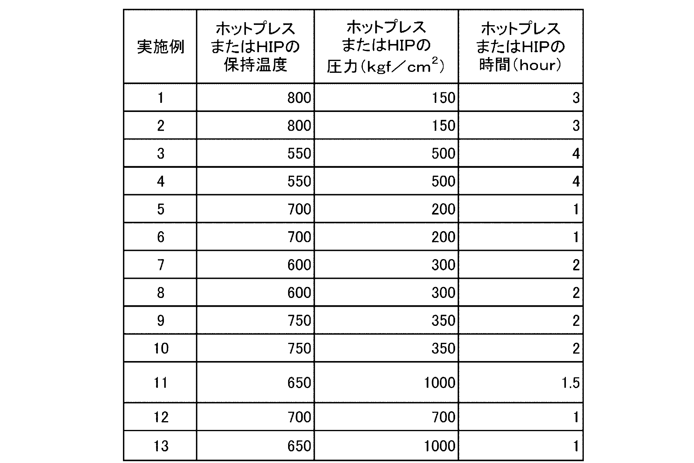
- sintering was performed by vacuum hot press using a graphite mold, and a sputtering target (Examples 1 to 10) of ⁇ 125 (mm) ⁇ 5 (mm) T was manufactured by grinding.
- the Cu—Ga alloy powder was prepared by gas atomization, classified and collected.
- hot isostatic pressing HIP (Examples 11 to 13)
- the mixed powder is filled in a mold and pressure-molded at 1500 kgf / cm 2 at room temperature.
- the obtained molded body was charged into a 0.5 mm-thick stainless steel container and then subjected to HIP through vacuum deaeration.
- Na 2 S particles and is displayed in black.
- image analysis software for example, WinRoof Ver 5.6.2 (manufactured by Mitani Corporation) can be used.
- a certain “threshold value” is set for the luminance (brightness) of each pixel of an image, and “0” is set if the threshold value is less than the threshold value, and “1” is set if the threshold value is greater.
- C Assuming that the maximum threshold value that does not select all the images is 100%, a threshold value of 32% is used to select a black side region showing Na 2 S particles. Then, the selected area four times shrink, the area when inflated 3 times and Na 2 S particles, measuring the size of the individual particles to obtain an average particle size. The magnification of shrinkage and expansion is, for example, 2.3%.
- the content of Ga and Na in the produced Cu—Ga—Na—S sputtering target was quantitatively analyzed using the ICP method (high frequency inductively coupled plasma method). S was analyzed using a carbon / sulfur analyzer (Horiba Seisakusho). *
- the sputtering target was formed into a 1000 nm thick glass plate with a thickness of 3.2 mm coated with a Mo sputtering film by direct current sputtering with a power density of 5 W / cm 2 using a magnetron sputtering apparatus.
- the thickness of the Mo sputtered film was 500 nm.
- the Ar pressure during sputtering was 1.3 Pa, and the distance between the sputtering target and the substrate was 70 mm. Note that the substrate is not heated during film formation.
- the number of occurrences of abnormal discharge during 10 minutes of continuous sputtering under the above conditions was automatically recorded by an arcing counter attached to the sputtering power source.
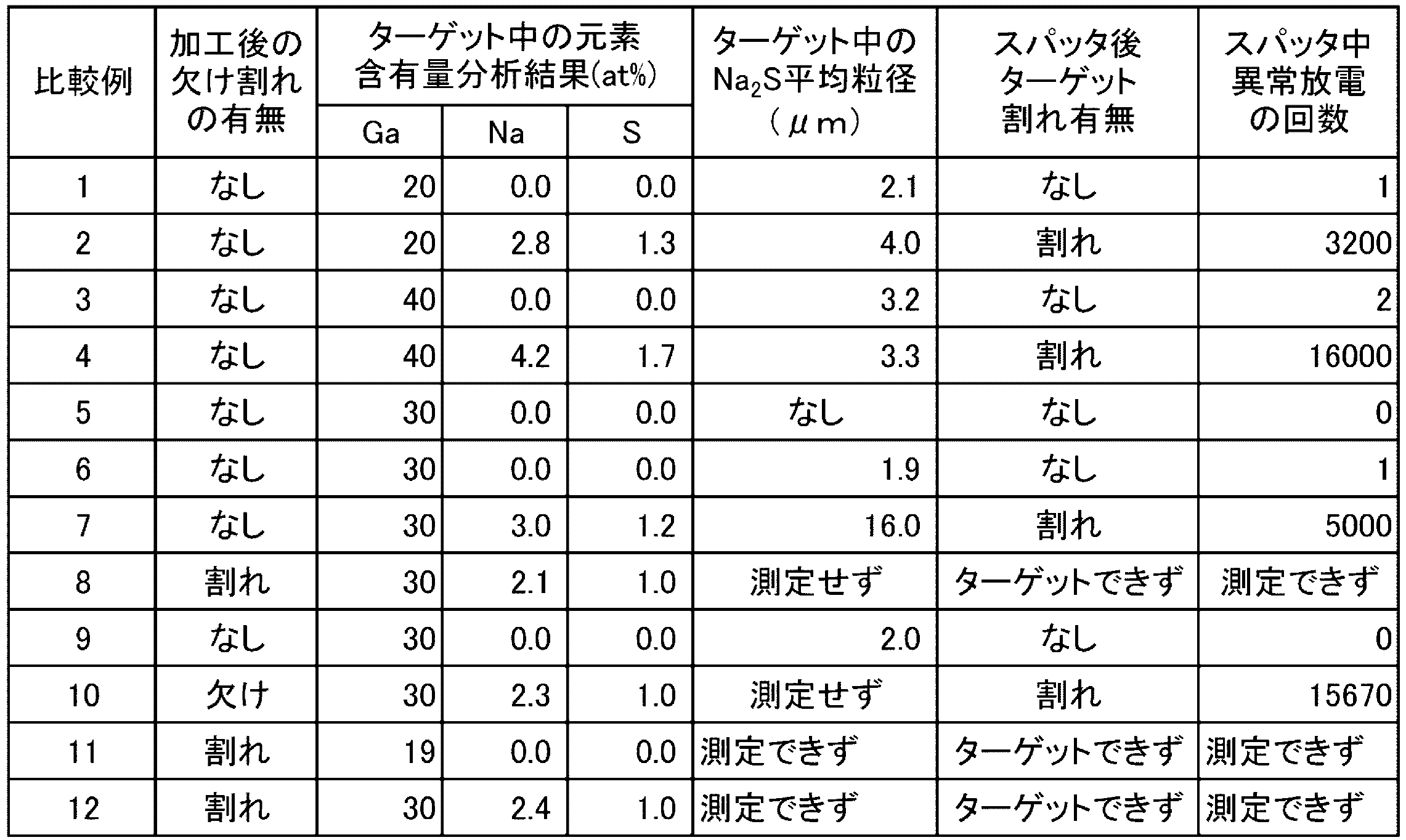
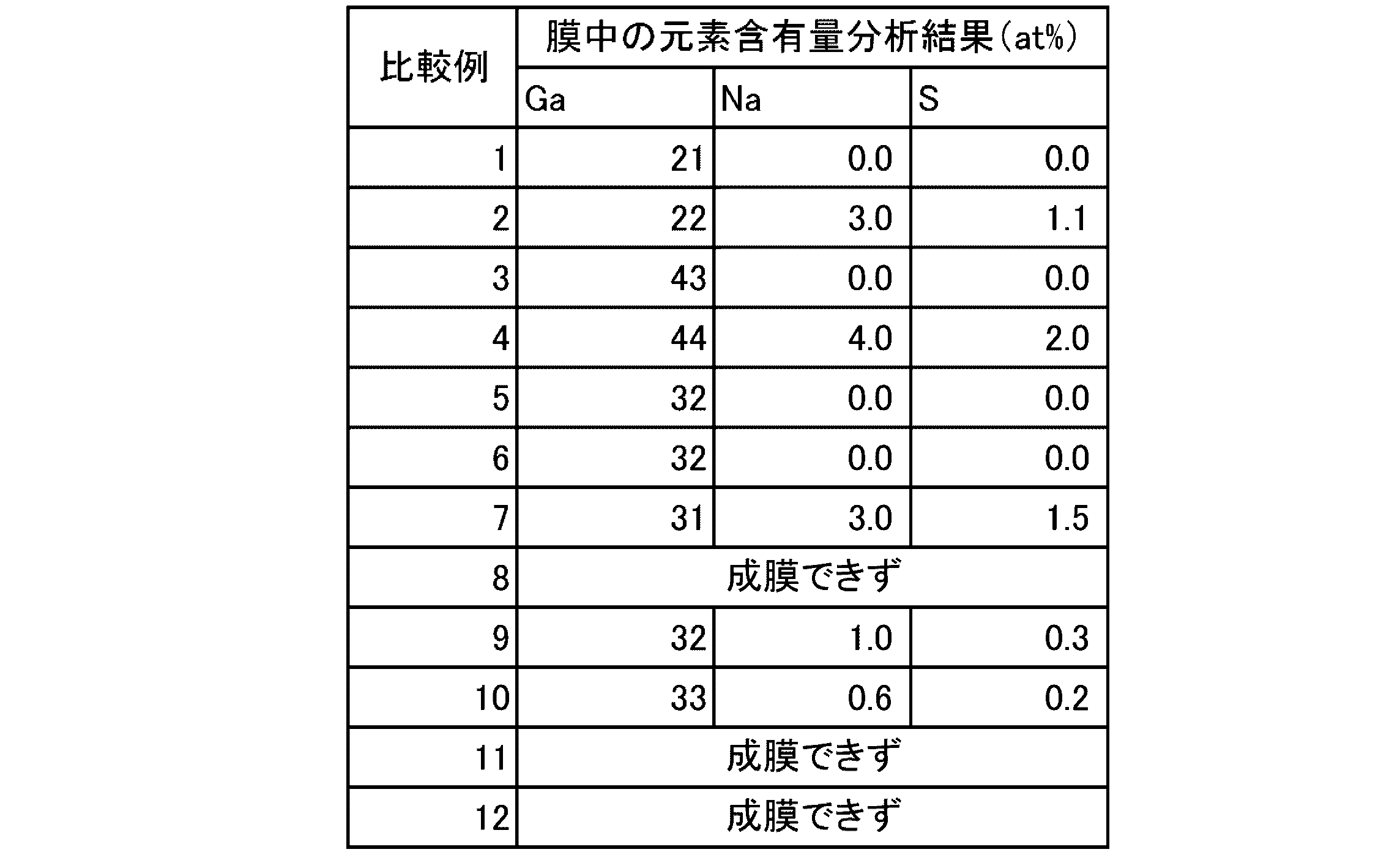
- “Comparative Example” Cu—Ga alloy powder and pure Cu powder having the component compositions and particle sizes shown in Table 5 were prepared, and Na 2 S powder similar to Table 1 was prepared. These raw materials were mixed at a designated time by a ball mill in the same manner as in Table 1. The mixture thus mixed was subjected to hot press sintering, HIP sintering or melt casting under the conditions shown in Table 6. The compounding composition of the sputtering target of the comparative example obtained in this way has a Na content outside the range of 0.05 to 2 at%.
- Comparative Examples 8 and 10 in Table 5 were not manufactured by the hot press method or the HIP method, but were performed at 1000 ° C. using a graphite crucible using a vacuum melting furnace. , And cast into an iron mold, cooled and then machined.
- the comparative example was evaluated in the same manner as in the above example.
- the evaluation results are shown in Table 7 and Table 8.
- Comparative Examples 8 and 10 produced by the melt casting method are cracked during machining. Further, in Comparative Examples 11 and 12 where the HIP temperature is lower than 500 ° C. and the pressure is lower than 300 kgf / cm 2 , the mechanical strength of the sintered body is low, cracking occurs during processing, and a sputtering target that can be sputtered cannot be produced. .
- Comparative Example 2 with a high Na content of 2.8 at% and a high holding temperature during hot pressing of 950 ° C., a comparative example 2 with a high Na content of 3 at% and a large average particle size of Na 2 S of 16 ⁇ m
- Example 7 and Comparative Example 4 in which the Na content is as high as 4.2 at% and the holding temperature during hot pressing is as low as 350 ° C., cracks are generated during sputtering.
- the number of abnormal discharges during sputtering was 10 or less, while in Comparative Examples 2, 4, 7, and 10, all occurred 1000 times or more. That is, Comparative Example 2 with a high Na content of 2.8 at% and a high holding temperature during hot pressing of 950 ° C., and Comparative Example 7 with a high Na content and a large Na 2 S average particle size of 16 ⁇ m Comparative Example 4 having a high Na content of 4.2 at% and a low holding temperature during hot pressing of 350 ° C., and a Comparative Example 4 having a high Na content of 2.3 at% and prepared by a dissolution method No. 10 has many abnormal discharges.
- the sputtering target of the present invention contains Ga: 20 to 40 at%, further contains Na: 0.05 to 2 at% and S: 0.025 to 1.0 at%, with the balance being Cu and inevitable. Since it has a component composition consisting of impurities, a Cu—Ga film containing Na that is effective in improving power generation efficiency can be formed by sputtering. Therefore, by forming a film by sputtering using the sputtering target of the present invention, Na can be added well, and a solar cell with high power generation efficiency can be manufactured. *
Abstract
Description
パッタリングターゲット及びその製造方法によれば、Ga:20~40at%を含有し、さらに、Na:0.05~2at%およびS:0.025~1.0at%を含有し、残部がCu及び不可避不純物からなる成分組成を有するので、スパッタ法により、発電効率の向上に有効なNaを含有したCu-Ga膜を成膜することができる。したがって、本発明のスパッタリングターゲットを用いてスパッタ法によりCu-Ga膜中にNaを良好に添加でき、発電効率の高い太陽電池を作製可能である。


、表6の条件でホットプレス焼結、HIP焼結または溶解鋳造を行った。このように得られた比較例のスパッタリングターゲットの配合組成は、Naの含有量が0.05~2at%の範囲外となっている。


Claims (6)
- Ga:20~40at%を含有し、 さらに、Na:0.05~2at%およびS:0.025~1.0at%を含有し、 残部がCu及び不可避不純物からなる成分組成を有することを特徴とするスパッタリングターゲット。
- 請求項1に記載のスパッタリングターゲットにおいて、 CuとGaとからなる金属相の素地中にNa2S相が分散している組織を有すると共に、前記Na2S相の平均粒径が5μm以下であることを特徴とするスパッタリングターゲット。
- 請求項1に記載のスパッタリングターゲットを作製する方法であって、 Na2S粉末とCu-Ga合金粉末との混合粉末、 又はNa2S粉末とCu-Ga合金粉末と純Cu粉末との混合粉末を、真空または不活性ガス雰囲気中でホットプレスする工程を有していることを特徴とするスパッタリングターゲットの製造方法。
- 請求項3に記載のスパッタリングターゲットの製造方法において、 前記ホットプレスを、ホットプレス時の保持温度が500℃~800℃で行うことを特徴とするスパッタリングターゲットの製造方法。
- 請求項1に記載のスパッタリングターゲットを作製する方法であって、 Na2S粉末とCu-Ga合金粉末との混合粉末、 又はNa2S粉末とCu-Ga合金粉末と純Cu粉末との混合粉末を、熱間静水圧プレスにより焼結する工程を有していることを特徴とするスパッタリングターゲットの製造方法。
- 請求項5に記載のスパッタリングターゲットの製造方法において、 前記熱間静水圧プレスを、温度:500~800℃、圧力:300kgf/cm2以上で行うことを特徴とするスパッタリングターゲットの製造方法。
Priority Applications (4)
| Application Number | Priority Date | Filing Date | Title |
|---|---|---|---|
| US13/579,223 US8968491B2 (en) | 2010-03-18 | 2011-03-08 | Sputtering target and method for producing same |
| CN201180008507.6A CN102753721B (zh) | 2010-03-18 | 2011-03-08 | 溅射靶及其制造方法 |
| KR1020127024254A KR20130028067A (ko) | 2010-03-18 | 2011-03-08 | 스퍼터링 타깃 및 그 제조 방법 |
| EP11755850.2A EP2548993B1 (en) | 2010-03-18 | 2011-03-08 | Sputtering target and manufacturing method therefor |
Applications Claiming Priority (4)
| Application Number | Priority Date | Filing Date | Title |
|---|---|---|---|
| JP2010063214 | 2010-03-18 | ||
| JP2010-063214 | 2010-03-18 | ||
| JP2011036656A JP4831258B2 (ja) | 2010-03-18 | 2011-02-23 | スパッタリングターゲット及びその製造方法 |
| JP2011-036656 | 2011-02-23 |
Publications (1)
| Publication Number | Publication Date |
|---|---|
| WO2011114657A1 true WO2011114657A1 (ja) | 2011-09-22 |
Family
ID=44648773
Family Applications (1)
| Application Number | Title | Priority Date | Filing Date |
|---|---|---|---|
| PCT/JP2011/001352 WO2011114657A1 (ja) | 2010-03-18 | 2011-03-08 | スパッタリングターゲット及びその製造方法 |
Country Status (7)
| Country | Link |
|---|---|
| US (1) | US8968491B2 (ja) |
| EP (1) | EP2548993B1 (ja) |
| JP (1) | JP4831258B2 (ja) |
| KR (1) | KR20130028067A (ja) |
| CN (1) | CN102753721B (ja) |
| TW (1) | TWI490348B (ja) |
| WO (1) | WO2011114657A1 (ja) |
Cited By (6)
| Publication number | Priority date | Publication date | Assignee | Title |
|---|---|---|---|---|
| WO2012147985A1 (ja) * | 2011-04-29 | 2012-11-01 | 三菱マテリアル株式会社 | スパッタリングターゲット及びその製造方法 |
| JP2013028837A (ja) * | 2011-07-28 | 2013-02-07 | Ulvac Japan Ltd | CuGaNa系スパッタリング用ターゲット及びその製造方法 |
| JP2013028836A (ja) * | 2011-07-28 | 2013-02-07 | Ulvac Japan Ltd | CuGaNa系スパッタリング用ターゲット及びその製造方法 |
| WO2013125716A1 (ja) * | 2012-02-24 | 2013-08-29 | 三菱マテリアル株式会社 | スパッタリングターゲット及びその製造方法 |
| JP2014224308A (ja) * | 2013-04-15 | 2014-12-04 | 三菱マテリアル株式会社 | スパッタリングターゲット及びその製造方法 |
| US10283332B2 (en) | 2012-10-17 | 2019-05-07 | Mitsubishi Materials Corporation | Cu—Ga binary alloy sputtering target and method of producing the same |
Families Citing this family (15)
| Publication number | Priority date | Publication date | Assignee | Title |
|---|---|---|---|---|
| JP5919738B2 (ja) * | 2011-11-10 | 2016-05-18 | 三菱マテリアル株式会社 | スパッタリングターゲットおよびその製造方法 |
| JP2013105885A (ja) * | 2011-11-14 | 2013-05-30 | Sumitomo Metal Mining Co Ltd | Cu−Ga合金スパッタリングターゲット及びその製造方法 |
| WO2013095070A1 (ko) * | 2011-12-22 | 2013-06-27 | (주)태광테크 | 저온분사를 이용한 스퍼터링 타겟의 제조방법 및 저온분사장치 |
| CN102751388B (zh) * | 2012-07-18 | 2015-03-11 | 林刘毓 | 一种铜铟镓硒薄膜太阳能电池的制备方法 |
| JP5928237B2 (ja) * | 2012-08-08 | 2016-06-01 | 住友金属鉱山株式会社 | Cu−Ga合金スパッタリングターゲット及びその製造方法 |
| JP2014037556A (ja) * | 2012-08-10 | 2014-02-27 | Mitsubishi Materials Corp | スパッタリングターゲット及びその製造方法 |
| JP5594618B1 (ja) * | 2013-02-25 | 2014-09-24 | 三菱マテリアル株式会社 | スパッタリングターゲット及びその製造方法 |
| JP6120076B2 (ja) | 2013-08-01 | 2017-04-26 | 三菱マテリアル株式会社 | Cu−Ga合金スパッタリングターゲット及びその製造方法 |
| JP5733357B2 (ja) * | 2013-08-02 | 2015-06-10 | 住友金属鉱山株式会社 | Cu−Ga合金スパッタリングターゲット |
| CN104416156B (zh) * | 2013-09-11 | 2016-08-17 | 安泰科技股份有限公司 | 铬铝合金靶材及其制备方法 |
| JP6665428B2 (ja) * | 2014-07-08 | 2020-03-13 | 三菱マテリアル株式会社 | Cu−Ga合金スパッタリングターゲット及びその製造方法 |
| TWI551704B (zh) * | 2015-05-21 | 2016-10-01 | China Steel Corp | Copper gallium alloy composite sodium element target manufacturing method |
| JP6436006B2 (ja) * | 2015-07-06 | 2018-12-12 | 三菱マテリアル株式会社 | スパッタリングターゲット及びその製造方法 |
| JP6794850B2 (ja) * | 2016-02-08 | 2020-12-02 | 三菱マテリアル株式会社 | スパッタリングターゲット及びスパッタリングターゲットの製造方法 |
| US10889887B2 (en) | 2016-08-22 | 2021-01-12 | Honeywell International Inc. | Chalcogenide sputtering target and method of making the same |
Citations (5)
| Publication number | Priority date | Publication date | Assignee | Title |
|---|---|---|---|---|
| JPH1074967A (ja) * | 1996-08-29 | 1998-03-17 | Moririka:Kk | 薄膜太陽電池 |
| JP3249408B2 (ja) | 1996-10-25 | 2002-01-21 | 昭和シェル石油株式会社 | 薄膜太陽電池の薄膜光吸収層の製造方法及び製造装置 |
| JP2003197941A (ja) * | 2001-12-28 | 2003-07-11 | Matsushita Electric Ind Co Ltd | 太陽電池の製造方法 |
| JP2007266626A (ja) * | 1994-12-01 | 2007-10-11 | Shell Solar Gmbh | 基板上に太陽電池を製造する方法及びカルコパイライト吸収層を有する太陽電池 |
| JP2009135299A (ja) | 2007-11-30 | 2009-06-18 | Showa Shell Sekiyu Kk | Cis系薄膜太陽電池の光吸収層の製造方法 |
Family Cites Families (13)
| Publication number | Priority date | Publication date | Assignee | Title |
|---|---|---|---|---|
| US20070163383A1 (en) * | 2004-02-19 | 2007-07-19 | Nanosolar, Inc. | High-throughput printing of nanostructured semiconductor precursor layer |
| JP4441467B2 (ja) * | 2004-12-24 | 2010-03-31 | 株式会社神戸製鋼所 | 曲げ加工性及び耐応力緩和特性を備えた銅合金 |
| JP4747751B2 (ja) * | 2005-05-09 | 2011-08-17 | 三菱マテリアル株式会社 | エレクトロルミネッセンス素子における蛍光体膜形成用高強度スパッタリングターゲット |
| EP2439296B1 (en) * | 2005-07-07 | 2013-08-28 | Kabushiki Kaisha Kobe Seiko Sho | Copper alloy having high strength and superior bending workability, and method for manufacturing copper alloy plates |
| JP5088464B2 (ja) * | 2006-06-08 | 2012-12-05 | 三菱マテリアル株式会社 | 高強度光記録媒体保護膜形成用スパッタリングターゲット |
| JP4811660B2 (ja) * | 2006-11-30 | 2011-11-09 | 三菱マテリアル株式会社 | 高Ga含有Cu−Ga二元系合金スパッタリングターゲットおよびその製造方法 |
| EP2184371B1 (en) * | 2007-08-07 | 2016-11-30 | Kabushiki Kaisha Kobe Seiko Sho | Copper alloy sheet |
| JP5061802B2 (ja) * | 2007-09-06 | 2012-10-31 | 三菱マテリアル株式会社 | 耐割れ性に優れたZrO2−In2O3系光記録媒体保護膜形成用スパッタリングターゲット |
| TWI353344B (en) | 2008-01-31 | 2011-12-01 | Method for producing copper indium chalcogenides p | |
| JP4540724B2 (ja) * | 2008-05-20 | 2010-09-08 | 昭和シェル石油株式会社 | Cis系薄膜太陽電池の製造方法 |
| JP4793504B2 (ja) * | 2009-11-06 | 2011-10-12 | 三菱マテリアル株式会社 | スパッタリングターゲット及びその製造方法 |
| WO2011083647A1 (ja) * | 2010-01-07 | 2011-07-14 | Jx日鉱日石金属株式会社 | Cu-Ga系スパッタリングターゲット、同ターゲットの製造方法、光吸収層及び該光吸収層を用いた太陽電池 |
| JP5730788B2 (ja) * | 2010-01-07 | 2015-06-10 | Jx日鉱日石金属株式会社 | スパッタリングターゲット及びスパッタリングターゲットの製造方法 |
-
2011
- 2011-02-23 JP JP2011036656A patent/JP4831258B2/ja not_active Expired - Fee Related
- 2011-03-08 KR KR1020127024254A patent/KR20130028067A/ko not_active Application Discontinuation
- 2011-03-08 EP EP11755850.2A patent/EP2548993B1/en not_active Not-in-force
- 2011-03-08 CN CN201180008507.6A patent/CN102753721B/zh not_active Expired - Fee Related
- 2011-03-08 WO PCT/JP2011/001352 patent/WO2011114657A1/ja active Application Filing
- 2011-03-08 US US13/579,223 patent/US8968491B2/en active Active
- 2011-03-14 TW TW100108559A patent/TWI490348B/zh not_active IP Right Cessation
Patent Citations (5)
| Publication number | Priority date | Publication date | Assignee | Title |
|---|---|---|---|---|
| JP2007266626A (ja) * | 1994-12-01 | 2007-10-11 | Shell Solar Gmbh | 基板上に太陽電池を製造する方法及びカルコパイライト吸収層を有する太陽電池 |
| JPH1074967A (ja) * | 1996-08-29 | 1998-03-17 | Moririka:Kk | 薄膜太陽電池 |
| JP3249408B2 (ja) | 1996-10-25 | 2002-01-21 | 昭和シェル石油株式会社 | 薄膜太陽電池の薄膜光吸収層の製造方法及び製造装置 |
| JP2003197941A (ja) * | 2001-12-28 | 2003-07-11 | Matsushita Electric Ind Co Ltd | 太陽電池の製造方法 |
| JP2009135299A (ja) | 2007-11-30 | 2009-06-18 | Showa Shell Sekiyu Kk | Cis系薄膜太陽電池の光吸収層の製造方法 |
Non-Patent Citations (3)
| Title |
|---|
| A. ROMEO: "Development of Thin-film Cu(In, Ga)Se2 and CdTe Solar Cells", PROG. PHOTOVOLT: RES. APPL., vol. 12, 2004, pages 93 - 111 |
| See also references of EP2548993A4 * |
| TOORU TANAKA ET AL.: "Preparation of Cu(In,Ga) 2Se3.5 thin films by radio frequency sputtering from stoichiometric Cu(In,Ga)Se2 and Na2Se mixture target", JOURNAL OF APPLIED PHYSICS, vol. 81, no. 11, June 1997 (1997-06-01), pages 7619 - 7622 * |
Cited By (12)
| Publication number | Priority date | Publication date | Assignee | Title |
|---|---|---|---|---|
| WO2012147985A1 (ja) * | 2011-04-29 | 2012-11-01 | 三菱マテリアル株式会社 | スパッタリングターゲット及びその製造方法 |
| US9660127B2 (en) | 2011-04-29 | 2017-05-23 | Mitsubishi Materials Corporation | Sputtering target and method for producing same |
| JP2013028837A (ja) * | 2011-07-28 | 2013-02-07 | Ulvac Japan Ltd | CuGaNa系スパッタリング用ターゲット及びその製造方法 |
| JP2013028836A (ja) * | 2011-07-28 | 2013-02-07 | Ulvac Japan Ltd | CuGaNa系スパッタリング用ターゲット及びその製造方法 |
| WO2013125716A1 (ja) * | 2012-02-24 | 2013-08-29 | 三菱マテリアル株式会社 | スパッタリングターゲット及びその製造方法 |
| JP2013199704A (ja) * | 2012-02-24 | 2013-10-03 | Mitsubishi Materials Corp | スパッタリングターゲット及びその製造方法 |
| EP2818574A4 (en) * | 2012-02-24 | 2015-11-11 | Mitsubishi Materials Corp | SPRAY TARGET AND METHOD FOR PRODUCING THE SAME |
| EP3141630A1 (en) * | 2012-02-24 | 2017-03-15 | Mitsubishi Materials Corporation | Sputtering target and method for producing same |
| US9607812B2 (en) | 2012-02-24 | 2017-03-28 | Mitsubishi Materials Corporation | Sputtering target and method for producing same |
| US10283332B2 (en) | 2012-10-17 | 2019-05-07 | Mitsubishi Materials Corporation | Cu—Ga binary alloy sputtering target and method of producing the same |
| JP2014224308A (ja) * | 2013-04-15 | 2014-12-04 | 三菱マテリアル株式会社 | スパッタリングターゲット及びその製造方法 |
| US9934949B2 (en) | 2013-04-15 | 2018-04-03 | Mitsubishi Materials Corporation | Sputtering target and production method of the same |
Also Published As
| Publication number | Publication date |
|---|---|
| CN102753721A (zh) | 2012-10-24 |
| EP2548993B1 (en) | 2016-08-24 |
| JP4831258B2 (ja) | 2011-12-07 |
| US8968491B2 (en) | 2015-03-03 |
| EP2548993A4 (en) | 2014-01-22 |
| KR20130028067A (ko) | 2013-03-18 |
| CN102753721B (zh) | 2015-02-11 |
| US20130001078A1 (en) | 2013-01-03 |
| EP2548993A1 (en) | 2013-01-23 |
| TW201139702A (en) | 2011-11-16 |
| TWI490348B (zh) | 2015-07-01 |
| JP2011214140A (ja) | 2011-10-27 |
Similar Documents
| Publication | Publication Date | Title |
|---|---|---|
| JP4831258B2 (ja) | スパッタリングターゲット及びその製造方法 | |
| JP4793504B2 (ja) | スパッタリングターゲット及びその製造方法 | |
| JP5725610B2 (ja) | スパッタリングターゲット及びその製造方法 | |
| JP5999357B2 (ja) | スパッタリングターゲット及びその製造方法 | |
| JP5919738B2 (ja) | スパッタリングターゲットおよびその製造方法 | |
| JP6365922B2 (ja) | スパッタリングターゲット及びその製造方法 | |
| TWI611028B (zh) | 濺鍍靶及其製造方法 | |
| JP2012246574A (ja) | スパッタリングターゲット及びその製造方法 | |
| JP6436006B2 (ja) | スパッタリングターゲット及びその製造方法 | |
| JP2014210943A (ja) | Cu−Ga合金ターゲット材およびその製造方法 | |
| JP5776902B2 (ja) | スパッタリングターゲット及びその製造方法 | |
| JP2014034721A (ja) | スパッタリングターゲット及びその製造方法 |
Legal Events
| Date | Code | Title | Description |
|---|---|---|---|
| WWE | Wipo information: entry into national phase |
Ref document number: 201180008507.6 Country of ref document: CN |
|
| 121 | Ep: the epo has been informed by wipo that ep was designated in this application |
Ref document number: 11755850 Country of ref document: EP Kind code of ref document: A1 |
|
| WWE | Wipo information: entry into national phase |
Ref document number: 7107/CHENP/2012 Country of ref document: IN |
|
| WWE | Wipo information: entry into national phase |
Ref document number: 13579223 Country of ref document: US |
|
| REEP | Request for entry into the european phase |
Ref document number: 2011755850 Country of ref document: EP |
|
| WWE | Wipo information: entry into national phase |
Ref document number: 2011755850 Country of ref document: EP |
|
| ENP | Entry into the national phase |
Ref document number: 20127024254 Country of ref document: KR Kind code of ref document: A |
|
| NENP | Non-entry into the national phase |
Ref country code: DE |