WO2010131451A1 - 電子デバイス用エピタキシャル基板およびその製造方法 - Google Patents
電子デバイス用エピタキシャル基板およびその製造方法 Download PDFInfo
- Publication number
- WO2010131451A1 WO2010131451A1 PCT/JP2010/003162 JP2010003162W WO2010131451A1 WO 2010131451 A1 WO2010131451 A1 WO 2010131451A1 JP 2010003162 W JP2010003162 W JP 2010003162W WO 2010131451 A1 WO2010131451 A1 WO 2010131451A1
- Authority
- WO
- WIPO (PCT)
- Prior art keywords
- layer
- buffer
- superlattice
- substrate
- laminate
- Prior art date
Links
- 239000000758 substrate Substances 0.000 title claims abstract description 109
- 238000000034 method Methods 0.000 title abstract description 15
- 239000000463 material Substances 0.000 claims abstract description 49
- 239000013078 crystal Substances 0.000 claims abstract description 31
- 150000004767 nitrides Chemical class 0.000 claims abstract description 20
- 238000004519 manufacturing process Methods 0.000 claims description 14
- 229910052799 carbon Inorganic materials 0.000 abstract description 2
- OKTJSMMVPCPJKN-UHFFFAOYSA-N Carbon Chemical compound [C] OKTJSMMVPCPJKN-UHFFFAOYSA-N 0.000 abstract 1
- 230000015556 catabolic process Effects 0.000 description 25
- 239000000203 mixture Substances 0.000 description 14
- 239000012535 impurity Substances 0.000 description 11
- 239000010408 film Substances 0.000 description 8
- 238000005259 measurement Methods 0.000 description 6
- IJGRMHOSHXDMSA-UHFFFAOYSA-N Atomic nitrogen Chemical compound N#N IJGRMHOSHXDMSA-UHFFFAOYSA-N 0.000 description 5
- 230000017525 heat dissipation Effects 0.000 description 5
- 230000003287 optical effect Effects 0.000 description 5
- 229910002704 AlGaN Inorganic materials 0.000 description 4
- QGZKDVFQNNGYKY-UHFFFAOYSA-N Ammonia Chemical compound N QGZKDVFQNNGYKY-UHFFFAOYSA-N 0.000 description 4
- 239000004065 semiconductor Substances 0.000 description 4
- UHOVQNZJYSORNB-UHFFFAOYSA-N Benzene Chemical compound C1=CC=CC=C1 UHOVQNZJYSORNB-UHFFFAOYSA-N 0.000 description 3
- 230000005669 field effect Effects 0.000 description 3
- 229910052739 hydrogen Inorganic materials 0.000 description 3
- 239000002184 metal Substances 0.000 description 3
- 229910052751 metal Inorganic materials 0.000 description 3
- RGSFGYAAUTVSQA-UHFFFAOYSA-N Cyclopentane Chemical compound C1CCCC1 RGSFGYAAUTVSQA-UHFFFAOYSA-N 0.000 description 2
- UFHFLCQGNIYNRP-UHFFFAOYSA-N Hydrogen Chemical compound [H][H] UFHFLCQGNIYNRP-UHFFFAOYSA-N 0.000 description 2
- 229910021529 ammonia Inorganic materials 0.000 description 2
- 230000000694 effects Effects 0.000 description 2
- 238000005530 etching Methods 0.000 description 2
- 238000002474 experimental method Methods 0.000 description 2
- 239000001257 hydrogen Substances 0.000 description 2
- 238000009413 insulation Methods 0.000 description 2
- 238000010030 laminating Methods 0.000 description 2
- VNWKTOKETHGBQD-UHFFFAOYSA-N methane Chemical compound C VNWKTOKETHGBQD-UHFFFAOYSA-N 0.000 description 2
- 229910052757 nitrogen Inorganic materials 0.000 description 2
- 229910052760 oxygen Inorganic materials 0.000 description 2
- 229910052710 silicon Inorganic materials 0.000 description 2
- 230000001629 suppression Effects 0.000 description 2
- JLTRXTDYQLMHGR-UHFFFAOYSA-N trimethylaluminium Chemical compound C[Al](C)C JLTRXTDYQLMHGR-UHFFFAOYSA-N 0.000 description 2
- XCZXGTMEAKBVPV-UHFFFAOYSA-N trimethylgallium Chemical compound C[Ga](C)C XCZXGTMEAKBVPV-UHFFFAOYSA-N 0.000 description 2
- OTMSDBZUPAUEDD-UHFFFAOYSA-N Ethane Chemical compound CC OTMSDBZUPAUEDD-UHFFFAOYSA-N 0.000 description 1
- VGGSQFUCUMXWEO-UHFFFAOYSA-N Ethene Chemical compound C=C VGGSQFUCUMXWEO-UHFFFAOYSA-N 0.000 description 1
- 239000005977 Ethylene Substances 0.000 description 1
- 229910002601 GaN Inorganic materials 0.000 description 1
- 229910001218 Gallium arsenide Inorganic materials 0.000 description 1
- 230000005355 Hall effect Effects 0.000 description 1
- 230000002411 adverse Effects 0.000 description 1
- 239000000956 alloy Substances 0.000 description 1
- 229910045601 alloy Inorganic materials 0.000 description 1
- HSFWRNGVRCDJHI-UHFFFAOYSA-N alpha-acetylene Natural products C#C HSFWRNGVRCDJHI-UHFFFAOYSA-N 0.000 description 1
- 229910052785 arsenic Inorganic materials 0.000 description 1
- 229910052796 boron Inorganic materials 0.000 description 1
- 230000003139 buffering effect Effects 0.000 description 1
- 239000000969 carrier Substances 0.000 description 1
- 239000012159 carrier gas Substances 0.000 description 1
- 238000005229 chemical vapour deposition Methods 0.000 description 1
- 238000011109 contamination Methods 0.000 description 1
- 238000005336 cracking Methods 0.000 description 1
- 238000000354 decomposition reaction Methods 0.000 description 1
- 238000000151 deposition Methods 0.000 description 1
- 230000008021 deposition Effects 0.000 description 1
- 229910001873 dinitrogen Inorganic materials 0.000 description 1
- 238000009826 distribution Methods 0.000 description 1
- 239000002019 doping agent Substances 0.000 description 1
- 125000001495 ethyl group Chemical group [H]C([H])([H])C([H])([H])* 0.000 description 1
- 125000002534 ethynyl group Chemical group [H]C#C* 0.000 description 1
- 229910052733 gallium Inorganic materials 0.000 description 1
- 239000007789 gas Substances 0.000 description 1
- 229910052732 germanium Inorganic materials 0.000 description 1
- 230000020169 heat generation Effects 0.000 description 1
- DMEGYFMYUHOHGS-UHFFFAOYSA-N heptamethylene Natural products C1CCCCCC1 DMEGYFMYUHOHGS-UHFFFAOYSA-N 0.000 description 1
- 238000010348 incorporation Methods 0.000 description 1
- 229910052738 indium Inorganic materials 0.000 description 1
- 229910052749 magnesium Inorganic materials 0.000 description 1
- 238000000691 measurement method Methods 0.000 description 1
- 239000007769 metal material Substances 0.000 description 1
- 238000002488 metal-organic chemical vapour deposition Methods 0.000 description 1
- 125000002496 methyl group Chemical group [H]C([H])([H])* 0.000 description 1
- 229910052698 phosphorus Inorganic materials 0.000 description 1
- 230000005855 radiation Effects 0.000 description 1
- 239000002994 raw material Substances 0.000 description 1
- 238000005092 sublimation method Methods 0.000 description 1
- 239000010409 thin film Substances 0.000 description 1
- 230000007704 transition Effects 0.000 description 1
- XLOMVQKBTHCTTD-UHFFFAOYSA-N zinc oxide Inorganic materials [Zn]=O XLOMVQKBTHCTTD-UHFFFAOYSA-N 0.000 description 1
Images


Classifications
-
- H—ELECTRICITY
- H01—ELECTRIC ELEMENTS
- H01L—SEMICONDUCTOR DEVICES NOT COVERED BY CLASS H10
- H01L21/00—Processes or apparatus adapted for the manufacture or treatment of semiconductor or solid state devices or of parts thereof
- H01L21/02—Manufacture or treatment of semiconductor devices or of parts thereof
- H01L21/04—Manufacture or treatment of semiconductor devices or of parts thereof the devices having at least one potential-jump barrier or surface barrier, e.g. PN junction, depletion layer or carrier concentration layer
- H01L21/18—Manufacture or treatment of semiconductor devices or of parts thereof the devices having at least one potential-jump barrier or surface barrier, e.g. PN junction, depletion layer or carrier concentration layer the devices having semiconductor bodies comprising elements of Group IV of the Periodic System or AIIIBV compounds with or without impurities, e.g. doping materials
- H01L21/20—Deposition of semiconductor materials on a substrate, e.g. epitaxial growth solid phase epitaxy
-
- H—ELECTRICITY
- H01—ELECTRIC ELEMENTS
- H01L—SEMICONDUCTOR DEVICES NOT COVERED BY CLASS H10
- H01L29/00—Semiconductor devices adapted for rectifying, amplifying, oscillating or switching, or capacitors or resistors with at least one potential-jump barrier or surface barrier, e.g. PN junction depletion layer or carrier concentration layer; Details of semiconductor bodies or of electrodes thereof ; Multistep manufacturing processes therefor
- H01L29/02—Semiconductor bodies ; Multistep manufacturing processes therefor
- H01L29/12—Semiconductor bodies ; Multistep manufacturing processes therefor characterised by the materials of which they are formed
- H01L29/20—Semiconductor bodies ; Multistep manufacturing processes therefor characterised by the materials of which they are formed including, apart from doping materials or other impurities, only AIIIBV compounds
- H01L29/207—Semiconductor bodies ; Multistep manufacturing processes therefor characterised by the materials of which they are formed including, apart from doping materials or other impurities, only AIIIBV compounds further characterised by the doping material
-
- H—ELECTRICITY
- H01—ELECTRIC ELEMENTS
- H01L—SEMICONDUCTOR DEVICES NOT COVERED BY CLASS H10
- H01L21/00—Processes or apparatus adapted for the manufacture or treatment of semiconductor or solid state devices or of parts thereof
- H01L21/02—Manufacture or treatment of semiconductor devices or of parts thereof
- H01L21/04—Manufacture or treatment of semiconductor devices or of parts thereof the devices having at least one potential-jump barrier or surface barrier, e.g. PN junction, depletion layer or carrier concentration layer
- H01L21/18—Manufacture or treatment of semiconductor devices or of parts thereof the devices having at least one potential-jump barrier or surface barrier, e.g. PN junction, depletion layer or carrier concentration layer the devices having semiconductor bodies comprising elements of Group IV of the Periodic System or AIIIBV compounds with or without impurities, e.g. doping materials
-
- H—ELECTRICITY
- H01—ELECTRIC ELEMENTS
- H01L—SEMICONDUCTOR DEVICES NOT COVERED BY CLASS H10
- H01L29/00—Semiconductor devices adapted for rectifying, amplifying, oscillating or switching, or capacitors or resistors with at least one potential-jump barrier or surface barrier, e.g. PN junction depletion layer or carrier concentration layer; Details of semiconductor bodies or of electrodes thereof ; Multistep manufacturing processes therefor
- H01L29/02—Semiconductor bodies ; Multistep manufacturing processes therefor
- H01L29/06—Semiconductor bodies ; Multistep manufacturing processes therefor characterised by their shape; characterised by the shapes, relative sizes, or dispositions of the semiconductor regions ; characterised by the concentration or distribution of impurities within semiconductor regions
- H01L29/10—Semiconductor bodies ; Multistep manufacturing processes therefor characterised by their shape; characterised by the shapes, relative sizes, or dispositions of the semiconductor regions ; characterised by the concentration or distribution of impurities within semiconductor regions with semiconductor regions connected to an electrode not carrying current to be rectified, amplified or switched and such electrode being part of a semiconductor device which comprises three or more electrodes
- H01L29/107—Substrate region of field-effect devices
- H01L29/1075—Substrate region of field-effect devices of field-effect transistors
-
- H—ELECTRICITY
- H01—ELECTRIC ELEMENTS
- H01L—SEMICONDUCTOR DEVICES NOT COVERED BY CLASS H10
- H01L29/00—Semiconductor devices adapted for rectifying, amplifying, oscillating or switching, or capacitors or resistors with at least one potential-jump barrier or surface barrier, e.g. PN junction depletion layer or carrier concentration layer; Details of semiconductor bodies or of electrodes thereof ; Multistep manufacturing processes therefor
- H01L29/02—Semiconductor bodies ; Multistep manufacturing processes therefor
- H01L29/12—Semiconductor bodies ; Multistep manufacturing processes therefor characterised by the materials of which they are formed
- H01L29/15—Structures with periodic or quasi periodic potential variation, e.g. multiple quantum wells, superlattices
- H01L29/151—Compositional structures
- H01L29/152—Compositional structures with quantum effects only in vertical direction, i.e. layered structures with quantum effects solely resulting from vertical potential variation
- H01L29/155—Comprising only semiconductor materials
-
- H—ELECTRICITY
- H01—ELECTRIC ELEMENTS
- H01L—SEMICONDUCTOR DEVICES NOT COVERED BY CLASS H10
- H01L29/00—Semiconductor devices adapted for rectifying, amplifying, oscillating or switching, or capacitors or resistors with at least one potential-jump barrier or surface barrier, e.g. PN junction depletion layer or carrier concentration layer; Details of semiconductor bodies or of electrodes thereof ; Multistep manufacturing processes therefor
- H01L29/02—Semiconductor bodies ; Multistep manufacturing processes therefor
- H01L29/12—Semiconductor bodies ; Multistep manufacturing processes therefor characterised by the materials of which they are formed
- H01L29/20—Semiconductor bodies ; Multistep manufacturing processes therefor characterised by the materials of which they are formed including, apart from doping materials or other impurities, only AIIIBV compounds
- H01L29/2003—Nitride compounds
-
- H—ELECTRICITY
- H01—ELECTRIC ELEMENTS
- H01L—SEMICONDUCTOR DEVICES NOT COVERED BY CLASS H10
- H01L29/00—Semiconductor devices adapted for rectifying, amplifying, oscillating or switching, or capacitors or resistors with at least one potential-jump barrier or surface barrier, e.g. PN junction depletion layer or carrier concentration layer; Details of semiconductor bodies or of electrodes thereof ; Multistep manufacturing processes therefor
- H01L29/66—Types of semiconductor device ; Multistep manufacturing processes therefor
- H01L29/68—Types of semiconductor device ; Multistep manufacturing processes therefor controllable by only the electric current supplied, or only the electric potential applied, to an electrode which does not carry the current to be rectified, amplified or switched
- H01L29/76—Unipolar devices, e.g. field effect transistors
- H01L29/772—Field effect transistors
- H01L29/778—Field effect transistors with two-dimensional charge carrier gas channel, e.g. HEMT ; with two-dimensional charge-carrier layer formed at a heterojunction interface
- H01L29/7786—Field effect transistors with two-dimensional charge carrier gas channel, e.g. HEMT ; with two-dimensional charge-carrier layer formed at a heterojunction interface with direct single heterostructure, i.e. with wide bandgap layer formed on top of active layer, e.g. direct single heterostructure MIS-like HEMT
-
- H—ELECTRICITY
- H01—ELECTRIC ELEMENTS
- H01L—SEMICONDUCTOR DEVICES NOT COVERED BY CLASS H10
- H01L21/00—Processes or apparatus adapted for the manufacture or treatment of semiconductor or solid state devices or of parts thereof
- H01L21/02—Manufacture or treatment of semiconductor devices or of parts thereof
- H01L21/02104—Forming layers
- H01L21/02365—Forming inorganic semiconducting materials on a substrate
- H01L21/02367—Substrates
- H01L21/0237—Materials
- H01L21/02373—Group 14 semiconducting materials
- H01L21/02378—Silicon carbide
-
- H—ELECTRICITY
- H01—ELECTRIC ELEMENTS
- H01L—SEMICONDUCTOR DEVICES NOT COVERED BY CLASS H10
- H01L21/00—Processes or apparatus adapted for the manufacture or treatment of semiconductor or solid state devices or of parts thereof
- H01L21/02—Manufacture or treatment of semiconductor devices or of parts thereof
- H01L21/02104—Forming layers
- H01L21/02365—Forming inorganic semiconducting materials on a substrate
- H01L21/02436—Intermediate layers between substrates and deposited layers
- H01L21/02439—Materials
- H01L21/02455—Group 13/15 materials
- H01L21/02458—Nitrides
-
- H—ELECTRICITY
- H01—ELECTRIC ELEMENTS
- H01L—SEMICONDUCTOR DEVICES NOT COVERED BY CLASS H10
- H01L21/00—Processes or apparatus adapted for the manufacture or treatment of semiconductor or solid state devices or of parts thereof
- H01L21/02—Manufacture or treatment of semiconductor devices or of parts thereof
- H01L21/02104—Forming layers
- H01L21/02365—Forming inorganic semiconducting materials on a substrate
- H01L21/02436—Intermediate layers between substrates and deposited layers
- H01L21/02439—Materials
- H01L21/02488—Insulating materials
-
- H—ELECTRICITY
- H01—ELECTRIC ELEMENTS
- H01L—SEMICONDUCTOR DEVICES NOT COVERED BY CLASS H10
- H01L21/00—Processes or apparatus adapted for the manufacture or treatment of semiconductor or solid state devices or of parts thereof
- H01L21/02—Manufacture or treatment of semiconductor devices or of parts thereof
- H01L21/02104—Forming layers
- H01L21/02365—Forming inorganic semiconducting materials on a substrate
- H01L21/02436—Intermediate layers between substrates and deposited layers
- H01L21/02494—Structure
- H01L21/02496—Layer structure
- H01L21/02505—Layer structure consisting of more than two layers
- H01L21/02507—Alternating layers, e.g. superlattice
-
- H—ELECTRICITY
- H01—ELECTRIC ELEMENTS
- H01L—SEMICONDUCTOR DEVICES NOT COVERED BY CLASS H10
- H01L21/00—Processes or apparatus adapted for the manufacture or treatment of semiconductor or solid state devices or of parts thereof
- H01L21/02—Manufacture or treatment of semiconductor devices or of parts thereof
- H01L21/02104—Forming layers
- H01L21/02365—Forming inorganic semiconducting materials on a substrate
- H01L21/02518—Deposited layers
- H01L21/02521—Materials
- H01L21/02538—Group 13/15 materials
- H01L21/0254—Nitrides
Landscapes
- Engineering & Computer Science (AREA)
- Microelectronics & Electronic Packaging (AREA)
- Power Engineering (AREA)
- Physics & Mathematics (AREA)
- Condensed Matter Physics & Semiconductors (AREA)
- General Physics & Mathematics (AREA)
- Computer Hardware Design (AREA)
- Ceramic Engineering (AREA)
- Manufacturing & Machinery (AREA)
- Junction Field-Effect Transistors (AREA)
- Crystals, And After-Treatments Of Crystals (AREA)
- Chemical Vapour Deposition (AREA)
Abstract
Description
(1)導電性SiC単結晶基板と、該SiC単結晶基板上に形成した絶縁層としてのバッファと、該バッファ上に複数層のIII族窒化物層をエピタキシャル成長させて形成した主積層体とを具え、横方向を電流導通方向とする電子デバイス用エピタキシャル基板であって、前記バッファは、前記SiC単結晶基板と接する初期成長層および該初期成長層上の超格子多層構造からなる超格子積層体を少なくとも有し、前記初期成長層はBa1Alb1Gac1Ind1N(0≦a1≦1, 0<b1≦1, 0≦c1≦1, 0≦d1≦1, a1+b1+c1+d1=1)材料からなり、かつ前記超格子積層体はBa2Alb2Gac2Ind2N(0≦a2≦1, 0≦b2≦1, 0≦c2≦1, 0≦d2≦1, a2+b2+c2+d2=1)材料からなる第1層および該第1層とはバンドギャップの異なるBa3Alb3Gac3Ind3N(0≦a3≦1, 0≦b3≦1, 0≦c3≦1, 0≦d3≦1, a3+b3+c3+d3=1)材料からなる第2層を交互に積層してなり、前記超格子積層体、または、前記主積層体の前記バッファ側の部分の少なくとも一方は、C濃度が1×10¹⁸/cm3以上であることを特徴とする電子デバイス用エピタキシャル基板。
第1の方法:Cを含む原料ガスを、III族窒化物成長中に別途添加する。メタン・エタン・エチレン・アセチレン・ベンゼン・シクロペンタン等が例示される。
第2の方法:有機金属中のメチル基・エチル基等を、成長III族窒化物成長条件によりエピタキシャル成長層に混入させる。有機金属の分解を抑えるように、成長温度・成長圧力・成長速度・成長時のアンモニア流量・水素流量・窒素流量等を適宜設定することにより、エピタキシャル成長層に添加されるC濃度を調整することが可能である。
なお、本願では、超格子積層体6のC濃度は、SIMSにより、超格子積層体6の厚さの1/2を除去した箇所の測定値とする。主積層体4のバッファ3側の部分4´のC濃度は、SIMSにより、前記部分4´の厚さの1/2を除去した箇所の測定値とする。
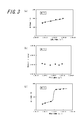
比抵抗がそれぞれ1×10-1Ω・cm、10Ω・cm、100Ω・cmの300μm厚の(0001)面3インチ6H-SiC単結晶基板上に、初期成長層(AlN材料:厚さ100nm)および超格子積層体(AlN:膜厚4nmとAl0.15Ga0.85N:膜厚25nm、合計85層)を成長させてバッファを形成し、この超格子積層体上にチャネル層(GaN材料:厚さ1.5μm)および電子供給層(Al0.25Ga0.75N材料:厚さ20nm)をエピタキシャル成長させてHEMT構造の主積層体を形成して試料1~3を得た。超格子積層体のC濃度を変化させ、主積層体のバッファ側の部分のC濃度は、いずれの結果も、1.5~2.0×10¹⁸/cm3の範囲であった。また、チャネル層の電子供給層側の部分は、C濃度が0.8~3.5×1016/cm3の範囲であった。各層の成長温度、圧力を表1に示す。表中P1を調整することによりC濃度を調整し、成膜圧力を下げることによりC濃度を増加させている。成長方法としてはMOCVD法を使用し、III族原料としては、TMA(トリメチルアルミニウム)・TMG(トリメチルガリウム)、V族原料としてはアンモニアを用い、キャリアガスとして、水素および窒素ガスを用いた。ここでいう成膜温度は、成長中に放射温度計を用いて測定した、基板自体の温度を意味する。なお、C濃度のSIMS測定は、エピタキシャル層側からエッチングを行い、Cameca製の測定装置で、イオン源としてCs-を用い、イオンエネルギーは8keVで行った。

縦方向:基板表面に80μmφからなるTi/Al積層構造のオーミック電極を形成し、オーミック電極外側を50nmの厚みでエッチングした後、基板裏面を金属板に接地し、両電極間に流れる電流値を電圧に対して測定した。
横方向:200μm□(四角)からなるTi/Al積層構造のオーミック電極を各々の一辺を10μmの距離を離して配置して形成し、前記オーミック電極周囲を150nmの厚みでエッチングした後、両電極間に流れる電流値を電圧に対して測定した。この際、空気中の放電を抑制するため、絶縁油で両電極間を絶縁している。また、基板裏面へのリークの影響をなくすため、基板下には絶縁板を配置している。
本実験例において、縦方向耐圧は縦方向の電流値を上記電極面積で単位面積当たりの値に換算した値が10-4A/cm2に達する電圧値で、横方向耐圧は横方向の電流値を上記電極の1辺の長さ当たりの値に換算した値が10-4A/cmに達する電圧値で、横方向リーク電流は横方向が100Vでの電流値で、それぞれ定義する。
超格子積層体6のC濃度は、SIMSにより、超格子積層体6の厚さの1/2を除去した箇所を測定することにより得た。主積層体4のバッファ3側の部分4´のC濃度は、SIMSにより、前記部分4´の厚さの1/2を除去した箇所を測定値することにより得た。
光学顕微鏡(100倍)で、全ての実験例で作製したエピタキシャル基板の表面を観察したが、クラックの発生は認められなかった。
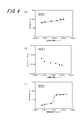
超格子積層体の成長圧力を10kPaとして、主積層体のバッファ側の部分のC濃度を変化させ、各層の成長温度、圧力を表2に示す条件で行ったこと以外は、実験例1の試料1~3と同様の方法により試料4~6を作製した。表中P2を調整することによりC濃度を調整し、成膜圧力を下げることによりC濃度を増加させている。超格子積層体のC濃度は、いずれの結果も1.5~2.5×10¹⁸/cm3の範囲であった。

光学顕微鏡(100倍)で、全ての実験例で作製したエピタキシャル基板の表面を観察したが、クラックの発生は認められなかった。
初期成長層を700℃で成長したGaN材料(厚さ:20nm)で形成し、各層の成長温度、圧力を表3に示す条件で行ったこと以外は、実験例1の試料2と同様の方法により試料7を作製した。

初期成長層を、Al0.5Ga0.5N材料とした以外は、実験例1の試料1~3と同様の方法により、試料8~10を作成し、同様の実験を行った。その結果、図3(a)、図3(b)および図3(c)と同様の結果が全ての試料で確認され、シート抵抗値450Ω/□以下(四角)、移動度は1550cm2/Vs以上と良好な特性を示すことが確認されていた。
光学顕微鏡(100倍)で、全ての実験例で作製したエピタキシャル基板の表面を観察したが、クラックの発生は認められなかった。
初期成長層を、Al0.5Ga0.5N材料とした以外は、実験例2の試料4~6と同様の方法により、試料11~13を作成し、同様の実験を行った。その結果、図4(a)、図4(b)および図4(c)と同様の結果が全ての試料で確認された。
光学顕微鏡(100倍)で、全ての実験例で作製したエピタキシャル基板の表面を観察したが、クラックの発生は認められなかった。
2 導電性SiC単結晶基板
3 バッファ
4 主積層体
4a チャネル層
4b 電子供給層
5 初期成長層
6 超格子積層体
6a 第1層
6b 第2層
Claims (7)
- 導電性SiC単結晶基板と、該SiC単結晶基板上に形成した絶縁層としてのバッファと、該バッファ上に複数層のIII族窒化物層をエピタキシャル成長させて形成した主積層体とを具え、横方向を電流導通方向とする電子デバイス用エピタキシャル基板であって、前記バッファは、前記SiC単結晶基板と接する初期成長層および該初期成長層上の超格子多層構造からなる超格子積層体を少なくとも有し、前記初期成長層はBa1Alb1Gac1Ind1N(0≦a1≦1, 0<b1≦1, 0≦c1≦1, 0≦d1≦1, a1+b1+c1+d1=1)材料からなり、かつ前記超格子積層体はBa2Alb2Gac2Ind2N(0≦a2≦1, 0≦b2≦1, 0≦c2≦1, 0≦d2≦1, a2+b2+c2+d2=1)材料からなる第1層および該第1層とはバンドギャップの異なるBa3Alb3Gac3Ind3N(0≦a3≦1, 0≦b3≦1, 0≦c3≦1, 0≦d3≦1, a3+b3+c3+d3=1)材料からなる第2層を交互に積層してなり、前記超格子積層体、または、前記主積層体の前記バッファ側の部分の少なくとも一方は、C濃度が1×10¹⁸/cm3以上であることを特徴とする電子デバイス用エピタキシャル基板。
- 前記超格子積層体、および、前記主積層体の前記バッファ側の部分は、ともにC濃度が1×10¹⁸/cm3以上である請求項1に記載の電子デバイス用エピタキシャル基板。
- 前記第1層がAlN材料からなり、前記第2層がAlb3Gac3N(a3=0, 0<b3≦0.5, 0.5≦c3<1, d3=0)材料からなる請求項1または2に記載の電子デバイス用エピタキシャル基板。
- 前記初期成長層がBa1Alb1Gac1Ind1N(0≦a1≦1, 0.5≦b1≦1, 0≦c1≦1, 0≦d1≦1, a1+b1+c1+d1=1)材料からなる請求項1、2または3に記載の電子デバイス用エピタキシャル基板。
- 前記初期成長層がAlN材料からなる請求項1、2または3に記載の電子デバイス用エピタキシャル基板。
- 導電性SiC単結晶基板と、該SiC単結晶基板上に形成した絶縁層としてのバッファと、該バッファ上に複数層のIII族窒化物層をエピタキシャル成長させて形成した主積層体とを具え、横方向を電流導通方向とする電子デバイス用エピタキシャル基板の製造方法であって、前記バッファは、前記SiC単結晶基板と接する初期成長層および該初期成長層上の超格子多層構造からなる超格子積層体を少なくとも有し、前記初期成長層はBa1Alb1Gac1Ind1N(0≦a1≦1, 0<b1≦1, 0≦c1≦1, 0≦d1≦1, a1+b1+c1+d1=1)材料からなり、かつ前記超格子積層体はBa2Alb2Gac2Ind2N(0≦a2≦1, 0≦b2≦1, 0≦c2≦1, 0≦d2≦1, a2+b2+c2+d2=1)材料からなる第1層および該第1層とはバンドギャップの異なるBa3Alb3Gac3Ind3N(0≦a3≦1, 0≦b3≦1, 0≦c3≦1, 0≦d3≦1, a3+b3+c3+d3=1)材料からなる第2層を交互に積層してなり、前記超格子積層体、または、前記主積層体の前記バッファ側の部分の少なくとも一方は、C濃度が1×10¹⁸/cm3以上であることを特徴とする電子デバイス用エピタキシャル基板の製造方法。
- 前記超格子積層体、および、前記主積層体の前記バッファ側の部分は、ともにC濃度が1×10¹⁸/cm3以上である請求項6に記載の電子デバイス用エピタキシャル基板の製造方法。
Priority Applications (4)
| Application Number | Priority Date | Filing Date | Title |
|---|---|---|---|
| KR1020117029263A KR101321625B1 (ko) | 2009-05-11 | 2010-05-10 | 전자 디바이스용 에피택셜 기판 및 그 제조방법 |
| US13/319,910 US8426893B2 (en) | 2009-05-11 | 2010-05-10 | Epitaxial substrate for electronic device and method of producing the same |
| CN201080031291.0A CN102460664B (zh) | 2009-05-11 | 2010-05-10 | 电子器件用外延衬底及其制造方法 |
| EP10774710.7A EP2432005A4 (en) | 2009-05-11 | 2010-05-10 | EPITACTICAL SUBSTRATE FOR ELECTRONIC EQUIPMENT AND METHOD FOR THE PRODUCTION THEREOF |
Applications Claiming Priority (4)
| Application Number | Priority Date | Filing Date | Title |
|---|---|---|---|
| JP2009114860 | 2009-05-11 | ||
| JP2009-114860 | 2009-05-11 | ||
| JP2010107821A JP4685961B2 (ja) | 2009-05-11 | 2010-05-10 | 電子デバイス用エピタキシャル基板およびその製造方法 |
| JP2010-107821 | 2010-05-10 |
Publications (1)
| Publication Number | Publication Date |
|---|---|
| WO2010131451A1 true WO2010131451A1 (ja) | 2010-11-18 |
Family
ID=43084836
Family Applications (1)
| Application Number | Title | Priority Date | Filing Date |
|---|---|---|---|
| PCT/JP2010/003162 WO2010131451A1 (ja) | 2009-05-11 | 2010-05-10 | 電子デバイス用エピタキシャル基板およびその製造方法 |
Country Status (7)
| Country | Link |
|---|---|
| US (1) | US8426893B2 (ja) |
| EP (1) | EP2432005A4 (ja) |
| JP (1) | JP4685961B2 (ja) |
| KR (1) | KR101321625B1 (ja) |
| CN (1) | CN102460664B (ja) |
| TW (1) | TWI466290B (ja) |
| WO (1) | WO2010131451A1 (ja) |
Cited By (1)
| Publication number | Priority date | Publication date | Assignee | Title |
|---|---|---|---|---|
| CN103208572A (zh) * | 2012-01-13 | 2013-07-17 | 同和电子科技有限公司 | Iii族氮化物外延基板以及使用该基板的深紫外发光元件 |
Families Citing this family (22)
| Publication number | Priority date | Publication date | Assignee | Title |
|---|---|---|---|---|
| JP5576771B2 (ja) * | 2009-11-04 | 2014-08-20 | Dowaエレクトロニクス株式会社 | Iii族窒化物エピタキシャル積層基板 |
| JP5228122B1 (ja) | 2012-03-08 | 2013-07-03 | 株式会社東芝 | 窒化物半導体素子及び窒化物半導体ウェーハ |
| CN102969341A (zh) * | 2012-11-09 | 2013-03-13 | 中国电子科技集团公司第五十五研究所 | 组分渐变AlyGa1-yN缓冲层的氮化物高电子迁移率晶体管外延结构 |
| JP5787417B2 (ja) * | 2013-05-14 | 2015-09-30 | コバレントマテリアル株式会社 | 窒化物半導体基板 |
| CN105431931A (zh) * | 2013-07-30 | 2016-03-23 | 住友化学株式会社 | 半导体基板以及半导体基板的制造方法 |
| JP2015053328A (ja) * | 2013-09-05 | 2015-03-19 | 富士通株式会社 | 半導体装置 |
| US9159788B2 (en) | 2013-12-31 | 2015-10-13 | Industrial Technology Research Institute | Nitride semiconductor structure |
| JP6174253B2 (ja) * | 2014-05-26 | 2017-08-02 | シャープ株式会社 | 窒化物系化合物半導体 |
| KR102439708B1 (ko) | 2014-05-27 | 2022-09-02 | 실라나 유브이 테크놀로지스 피티이 리미티드 | 광전자 디바이스 |
| WO2015181657A1 (en) | 2014-05-27 | 2015-12-03 | The Silanna Group Pty Limited | Advanced electronic device structures using semiconductor structures and superlattices |
| US11322643B2 (en) | 2014-05-27 | 2022-05-03 | Silanna UV Technologies Pte Ltd | Optoelectronic device |
| JP6986349B2 (ja) | 2014-05-27 | 2021-12-22 | シランナ・ユー・ブイ・テクノロジーズ・プライベート・リミテッドSilanna Uv Technologies Pte Ltd | n型超格子及びp型超格子を備える電子デバイス |
| US9608103B2 (en) * | 2014-10-02 | 2017-03-28 | Toshiba Corporation | High electron mobility transistor with periodically carbon doped gallium nitride |
| AT518350A3 (de) * | 2014-11-07 | 2019-06-15 | Sumitomo Chemical Co | Halbleiterwafer und Verfahren zum Prüfen eines Halbleiterwafers |
| US11335799B2 (en) * | 2015-03-26 | 2022-05-17 | Chih-Shu Huang | Group-III nitride semiconductor device and method for fabricating the same |
| US10403746B2 (en) | 2015-03-31 | 2019-09-03 | Swegan Ab | Heterostructure and method of its production |
| JP6615075B2 (ja) * | 2016-09-15 | 2019-12-04 | サンケン電気株式会社 | 半導体デバイス用基板、半導体デバイス、及び、半導体デバイス用基板の製造方法 |
| JP6796467B2 (ja) * | 2016-11-30 | 2020-12-09 | 住友化学株式会社 | 半導体基板 |
| JP6376257B2 (ja) * | 2017-09-01 | 2018-08-22 | 富士通株式会社 | 半導体装置 |
| CN112750904B (zh) | 2019-10-30 | 2024-01-02 | 联华电子股份有限公司 | 具有应力松弛层的半导体元件 |
| JP2022036462A (ja) * | 2020-08-24 | 2022-03-08 | エア・ウォーター株式会社 | 化合物半導体基板および化合物半導体デバイス |
| TWI818379B (zh) * | 2021-12-08 | 2023-10-11 | 財團法人工業技術研究院 | 高電子遷移率電晶體元件 |
Citations (8)
| Publication number | Priority date | Publication date | Assignee | Title |
|---|---|---|---|---|
| JP2002359255A (ja) * | 2001-05-31 | 2002-12-13 | Ngk Insulators Ltd | 半導体素子 |
| JP2005085852A (ja) | 2003-09-05 | 2005-03-31 | Furukawa Electric Co Ltd:The | 半導体電子デバイス |
| JP2005512327A (ja) * | 2001-12-03 | 2005-04-28 | クリー インコーポレイテッド | へテロ接合トランジスタ及びその製造方法 |
| JP2006114655A (ja) * | 2004-10-14 | 2006-04-27 | Hitachi Cable Ltd | 半導体エピタキシャルウェハ及び電界効果トランジスタ |
| JP2007251144A (ja) * | 2006-02-20 | 2007-09-27 | Furukawa Electric Co Ltd:The | 半導体素子 |
| JP2008085123A (ja) | 2006-09-28 | 2008-04-10 | Covalent Materials Corp | 化合物半導体デバイス用基板およびそれを用いた化合物半導体デバイス |
| JP2008171843A (ja) * | 2007-01-05 | 2008-07-24 | Furukawa Electric Co Ltd:The | 半導体電子デバイス |
| JP2008227478A (ja) * | 2007-02-16 | 2008-09-25 | Sumitomo Chemical Co Ltd | ガリウムナイトライド系エピタキシャル結晶及びその製造方法 |
Family Cites Families (8)
| Publication number | Priority date | Publication date | Assignee | Title |
|---|---|---|---|---|
| KR100538313B1 (ko) * | 1997-01-09 | 2005-12-21 | 니치아 카가쿠 고교 가부시키가이샤 | 질화물반도체소자 |
| US6995473B2 (en) * | 2002-12-19 | 2006-02-07 | Matsushita Electric Industrial Co., Ltd. | Stacked semiconductor transistors |
| JP4530171B2 (ja) * | 2003-08-08 | 2010-08-25 | サンケン電気株式会社 | 半導体装置 |
| JP4509031B2 (ja) * | 2003-09-05 | 2010-07-21 | サンケン電気株式会社 | 窒化物半導体装置 |
| JP4542912B2 (ja) * | 2005-02-02 | 2010-09-15 | 株式会社東芝 | 窒素化合物半導体素子 |
| US7491626B2 (en) * | 2005-06-20 | 2009-02-17 | Sensor Electronic Technology, Inc. | Layer growth using metal film and/or islands |
| JP2007214384A (ja) * | 2006-02-09 | 2007-08-23 | Rohm Co Ltd | 窒化物半導体素子 |
| JP5099008B2 (ja) * | 2006-07-26 | 2012-12-12 | 富士通株式会社 | SiC基板を用いた化合物半導体装置とその製造方法 |
-
2010
- 2010-05-10 US US13/319,910 patent/US8426893B2/en active Active
- 2010-05-10 JP JP2010107821A patent/JP4685961B2/ja active Active
- 2010-05-10 KR KR1020117029263A patent/KR101321625B1/ko active IP Right Grant
- 2010-05-10 CN CN201080031291.0A patent/CN102460664B/zh active Active
- 2010-05-10 WO PCT/JP2010/003162 patent/WO2010131451A1/ja active Application Filing
- 2010-05-10 EP EP10774710.7A patent/EP2432005A4/en not_active Withdrawn
- 2010-05-11 TW TW099114928A patent/TWI466290B/zh active
Patent Citations (8)
| Publication number | Priority date | Publication date | Assignee | Title |
|---|---|---|---|---|
| JP2002359255A (ja) * | 2001-05-31 | 2002-12-13 | Ngk Insulators Ltd | 半導体素子 |
| JP2005512327A (ja) * | 2001-12-03 | 2005-04-28 | クリー インコーポレイテッド | へテロ接合トランジスタ及びその製造方法 |
| JP2005085852A (ja) | 2003-09-05 | 2005-03-31 | Furukawa Electric Co Ltd:The | 半導体電子デバイス |
| JP2006114655A (ja) * | 2004-10-14 | 2006-04-27 | Hitachi Cable Ltd | 半導体エピタキシャルウェハ及び電界効果トランジスタ |
| JP2007251144A (ja) * | 2006-02-20 | 2007-09-27 | Furukawa Electric Co Ltd:The | 半導体素子 |
| JP2008085123A (ja) | 2006-09-28 | 2008-04-10 | Covalent Materials Corp | 化合物半導体デバイス用基板およびそれを用いた化合物半導体デバイス |
| JP2008171843A (ja) * | 2007-01-05 | 2008-07-24 | Furukawa Electric Co Ltd:The | 半導体電子デバイス |
| JP2008227478A (ja) * | 2007-02-16 | 2008-09-25 | Sumitomo Chemical Co Ltd | ガリウムナイトライド系エピタキシャル結晶及びその製造方法 |
Non-Patent Citations (1)
| Title |
|---|
| See also references of EP2432005A4 |
Cited By (1)
| Publication number | Priority date | Publication date | Assignee | Title |
|---|---|---|---|---|
| CN103208572A (zh) * | 2012-01-13 | 2013-07-17 | 同和电子科技有限公司 | Iii族氮化物外延基板以及使用该基板的深紫外发光元件 |
Also Published As
| Publication number | Publication date |
|---|---|
| JP2010287882A (ja) | 2010-12-24 |
| CN102460664B (zh) | 2014-08-13 |
| EP2432005A1 (en) | 2012-03-21 |
| CN102460664A (zh) | 2012-05-16 |
| EP2432005A4 (en) | 2015-05-27 |
| TWI466290B (zh) | 2014-12-21 |
| JP4685961B2 (ja) | 2011-05-18 |
| US20120091435A1 (en) | 2012-04-19 |
| KR20120023761A (ko) | 2012-03-13 |
| TW201101486A (en) | 2011-01-01 |
| US8426893B2 (en) | 2013-04-23 |
| KR101321625B1 (ko) | 2013-10-23 |
Similar Documents
| Publication | Publication Date | Title |
|---|---|---|
| JP4685961B2 (ja) | 電子デバイス用エピタキシャル基板およびその製造方法 | |
| JP4677499B2 (ja) | 電子デバイス用エピタキシャル基板およびその製造方法 | |
| CN107799583B (zh) | 在异质基底上的第III族氮化物缓冲层结构的p型掺杂 | |
| JP5787417B2 (ja) | 窒化物半導体基板 | |
| KR102171509B1 (ko) | n형 질화알루미늄 단결정 기판 및 수직형 질화물 반도체 디바이스 | |
| US8653561B2 (en) | III-nitride semiconductor electronic device, and method of fabricating III-nitride semiconductor electronic device | |
| JP2011082494A (ja) | 化合物半導体基板 | |
| WO2013116747A1 (en) | Buffer layer structures suited for iii-nitride devices with foreign substrates | |
| US8946863B2 (en) | Epitaxial substrate for electronic device comprising a high resistance single crystal substrate on a low resistance single crystal substrate, and method of manufacturing | |
| JP5788296B2 (ja) | 窒化物半導体基板及びその製造方法 | |
| JP5622499B2 (ja) | 電子デバイス用エピタキシャル基板およびその製造方法 | |
| JP4888537B2 (ja) | Iii族窒化物半導体積層ウェハ及びiii族窒化物半導体デバイス | |
| WO2015045412A1 (ja) | 電子デバイス用エピタキシャル基板およびその製造方法 | |
| JP6173493B2 (ja) | 半導体素子用のエピタキシャル基板およびその製造方法 | |
| JP2015070091A (ja) | Iii族窒化物半導体基板 | |
| JP2014022698A (ja) | 窒化物半導体成長用Si基板およびそれを用いた電子デバイス用エピタキシャル基板およびそれらの製造方法 | |
| JP2018137432A (ja) | 窒化物半導体基板およびその製造方法 | |
| JP2008085123A (ja) | 化合物半導体デバイス用基板およびそれを用いた化合物半導体デバイス | |
| JP2014241387A (ja) | 基板、基板の製造方法、及び電子装置 | |
| JP2015103665A (ja) | 窒化物半導体エピタキシャルウエハおよび窒化物半導体 | |
| JP2012064977A (ja) | Iii族窒化物半導体積層ウェハ及びiii族窒化物半導体デバイス | |
| JP6404738B2 (ja) | 電子デバイス用エピタキシャル基板および高電子移動度トランジスタならびにそれらの製造方法 | |
| JP2011258782A (ja) | 窒化物半導体基板 | |
| JP5230560B2 (ja) | 化合物半導体基板とその製造方法 | |
| JP2006216576A (ja) | 化合物半導体デバイス |
Legal Events
| Date | Code | Title | Description |
|---|---|---|---|
| WWE | Wipo information: entry into national phase |
Ref document number: 201080031291.0 Country of ref document: CN |
|
| 121 | Ep: the epo has been informed by wipo that ep was designated in this application |
Ref document number: 10774710 Country of ref document: EP Kind code of ref document: A1 |
|
| NENP | Non-entry into the national phase |
Ref country code: DE |
|
| WWE | Wipo information: entry into national phase |
Ref document number: 2010774710 Country of ref document: EP |
|
| WWE | Wipo information: entry into national phase |
Ref document number: 13319910 Country of ref document: US |
|
| ENP | Entry into the national phase |
Ref document number: 20117029263 Country of ref document: KR Kind code of ref document: A |