WO2010090111A1 - Procédé de découpe d'une pièce - Google Patents
Procédé de découpe d'une pièce Download PDFInfo
- Publication number
- WO2010090111A1 WO2010090111A1 PCT/JP2010/051047 JP2010051047W WO2010090111A1 WO 2010090111 A1 WO2010090111 A1 WO 2010090111A1 JP 2010051047 W JP2010051047 W JP 2010051047W WO 2010090111 A1 WO2010090111 A1 WO 2010090111A1
- Authority
- WO
- WIPO (PCT)
- Prior art keywords
- modified region
- workpiece
- region
- modified
- silicon substrate
- Prior art date
Links
Images


Classifications
-
- B—PERFORMING OPERATIONS; TRANSPORTING
- B23—MACHINE TOOLS; METAL-WORKING NOT OTHERWISE PROVIDED FOR
- B23K—SOLDERING OR UNSOLDERING; WELDING; CLADDING OR PLATING BY SOLDERING OR WELDING; CUTTING BY APPLYING HEAT LOCALLY, e.g. FLAME CUTTING; WORKING BY LASER BEAM
- B23K26/00—Working by laser beam, e.g. welding, cutting or boring
- B23K26/36—Removing material
- B23K26/38—Removing material by boring or cutting
-
- B—PERFORMING OPERATIONS; TRANSPORTING
- B23—MACHINE TOOLS; METAL-WORKING NOT OTHERWISE PROVIDED FOR
- B23K—SOLDERING OR UNSOLDERING; WELDING; CLADDING OR PLATING BY SOLDERING OR WELDING; CUTTING BY APPLYING HEAT LOCALLY, e.g. FLAME CUTTING; WORKING BY LASER BEAM
- B23K26/00—Working by laser beam, e.g. welding, cutting or boring
- B23K26/02—Positioning or observing the workpiece, e.g. with respect to the point of impact; Aligning, aiming or focusing the laser beam
- B23K26/03—Observing, e.g. monitoring, the workpiece
-
- B—PERFORMING OPERATIONS; TRANSPORTING
- B23—MACHINE TOOLS; METAL-WORKING NOT OTHERWISE PROVIDED FOR
- B23K—SOLDERING OR UNSOLDERING; WELDING; CLADDING OR PLATING BY SOLDERING OR WELDING; CUTTING BY APPLYING HEAT LOCALLY, e.g. FLAME CUTTING; WORKING BY LASER BEAM
- B23K26/00—Working by laser beam, e.g. welding, cutting or boring
- B23K26/02—Positioning or observing the workpiece, e.g. with respect to the point of impact; Aligning, aiming or focusing the laser beam
- B23K26/06—Shaping the laser beam, e.g. by masks or multi-focusing
- B23K26/062—Shaping the laser beam, e.g. by masks or multi-focusing by direct control of the laser beam
- B23K26/0622—Shaping the laser beam, e.g. by masks or multi-focusing by direct control of the laser beam by shaping pulses
-
- B—PERFORMING OPERATIONS; TRANSPORTING
- B23—MACHINE TOOLS; METAL-WORKING NOT OTHERWISE PROVIDED FOR
- B23K—SOLDERING OR UNSOLDERING; WELDING; CLADDING OR PLATING BY SOLDERING OR WELDING; CUTTING BY APPLYING HEAT LOCALLY, e.g. FLAME CUTTING; WORKING BY LASER BEAM
- B23K26/00—Working by laser beam, e.g. welding, cutting or boring
- B23K26/08—Devices involving relative movement between laser beam and workpiece
- B23K26/083—Devices involving movement of the workpiece in at least one axial direction
- B23K26/0853—Devices involving movement of the workpiece in at least in two axial directions, e.g. in a plane
-
- B—PERFORMING OPERATIONS; TRANSPORTING
- B23—MACHINE TOOLS; METAL-WORKING NOT OTHERWISE PROVIDED FOR
- B23K—SOLDERING OR UNSOLDERING; WELDING; CLADDING OR PLATING BY SOLDERING OR WELDING; CUTTING BY APPLYING HEAT LOCALLY, e.g. FLAME CUTTING; WORKING BY LASER BEAM
- B23K26/00—Working by laser beam, e.g. welding, cutting or boring
- B23K26/36—Removing material
- B23K26/40—Removing material taking account of the properties of the material involved
-
- B—PERFORMING OPERATIONS; TRANSPORTING
- B23—MACHINE TOOLS; METAL-WORKING NOT OTHERWISE PROVIDED FOR
- B23K—SOLDERING OR UNSOLDERING; WELDING; CLADDING OR PLATING BY SOLDERING OR WELDING; CUTTING BY APPLYING HEAT LOCALLY, e.g. FLAME CUTTING; WORKING BY LASER BEAM
- B23K26/00—Working by laser beam, e.g. welding, cutting or boring
- B23K26/50—Working by transmitting the laser beam through or within the workpiece
- B23K26/53—Working by transmitting the laser beam through or within the workpiece for modifying or reforming the material inside the workpiece, e.g. for producing break initiation cracks
-
- C—CHEMISTRY; METALLURGY
- C03—GLASS; MINERAL OR SLAG WOOL
- C03B—MANUFACTURE, SHAPING, OR SUPPLEMENTARY PROCESSES
- C03B33/00—Severing cooled glass
- C03B33/02—Cutting or splitting sheet glass or ribbons; Apparatus or machines therefor
- C03B33/0222—Scoring using a focussed radiation beam, e.g. laser
-
- H—ELECTRICITY
- H01—ELECTRIC ELEMENTS
- H01L—SEMICONDUCTOR DEVICES NOT COVERED BY CLASS H10
- H01L21/00—Processes or apparatus adapted for the manufacture or treatment of semiconductor or solid state devices or of parts thereof
- H01L21/67—Apparatus specially adapted for handling semiconductor or electric solid state devices during manufacture or treatment thereof; Apparatus specially adapted for handling wafers during manufacture or treatment of semiconductor or electric solid state devices or components ; Apparatus not specifically provided for elsewhere
- H01L21/67005—Apparatus not specifically provided for elsewhere
- H01L21/67011—Apparatus for manufacture or treatment
- H01L21/67092—Apparatus for mechanical treatment
-
- H—ELECTRICITY
- H01—ELECTRIC ELEMENTS
- H01L—SEMICONDUCTOR DEVICES NOT COVERED BY CLASS H10
- H01L21/00—Processes or apparatus adapted for the manufacture or treatment of semiconductor or solid state devices or of parts thereof
- H01L21/70—Manufacture or treatment of devices consisting of a plurality of solid state components formed in or on a common substrate or of parts thereof; Manufacture of integrated circuit devices or of parts thereof
- H01L21/77—Manufacture or treatment of devices consisting of a plurality of solid state components or integrated circuits formed in, or on, a common substrate
- H01L21/78—Manufacture or treatment of devices consisting of a plurality of solid state components or integrated circuits formed in, or on, a common substrate with subsequent division of the substrate into plural individual devices
-
- B—PERFORMING OPERATIONS; TRANSPORTING
- B23—MACHINE TOOLS; METAL-WORKING NOT OTHERWISE PROVIDED FOR
- B23K—SOLDERING OR UNSOLDERING; WELDING; CLADDING OR PLATING BY SOLDERING OR WELDING; CUTTING BY APPLYING HEAT LOCALLY, e.g. FLAME CUTTING; WORKING BY LASER BEAM
- B23K2101/00—Articles made by soldering, welding or cutting
- B23K2101/36—Electric or electronic devices
- B23K2101/40—Semiconductor devices
-
- B—PERFORMING OPERATIONS; TRANSPORTING
- B23—MACHINE TOOLS; METAL-WORKING NOT OTHERWISE PROVIDED FOR
- B23K—SOLDERING OR UNSOLDERING; WELDING; CLADDING OR PLATING BY SOLDERING OR WELDING; CUTTING BY APPLYING HEAT LOCALLY, e.g. FLAME CUTTING; WORKING BY LASER BEAM
- B23K2103/00—Materials to be soldered, welded or cut
- B23K2103/50—Inorganic material, e.g. metals, not provided for in B23K2103/02 – B23K2103/26
Definitions
- the present invention relates to a processing object cutting method for cutting a plate-shaped processing object including a silicon substrate along a planned cutting line.
- laser light having a wavelength of 1300 nm has a higher transmittance in the silicon substrate than laser light having a wavelength of 1064 nm. Therefore, when laser light having a wavelength of 1300 nm is used, even if the laser beam is deep from the laser light incident surface of the silicon substrate, the laser beam having a wavelength of A quality region can be formed. Therefore, when a plurality of modified regions are formed in the thickness direction of the silicon substrate along the planned cutting line and the workpiece is cut, the number of columns of the modified regions is reduced and the tact time is reduced. Shortening can be achieved.
- the present invention has been made in view of such circumstances, and can reduce the number of columns of modified regions formed in the thickness direction of the silicon substrate along the planned cutting line, and includes a silicon substrate. It aims at providing the processing object cutting method which can cut
- a processing object cutting method irradiates a plate-like processing object provided with a silicon substrate with a laser beam, thereby forming a silicon substrate along a planned cutting line of the processing object.
- the modified region is formed, and the workpiece is cut along the planned cutting line using the modified region as a starting point for cutting, and the first modified region is formed as the modified region.
- a first crack is generated on one main surface of the workpiece from the first modified region along the planned cutting line, and the other main surface of the workpiece is formed with respect to the first modified region.
- the first modified region is connected to the first crack. From the second modified region along the planned cutting line A step of generating a second crack on the principal surface of the other side and a stress on the workpiece to connect the first crack and the second crack, and the workpiece to be processed along the planned cutting line And a step of cutting.
- one of the objects to be processed from the first reformed region in a state where the non-modified region is interposed between the first modified region and the second modified region.
- a first crack is generated in the main surface
- a second crack is generated in the other main surface of the workpiece from the second modified region.
- the process target object is cut
- the meandering of the crack in the main surface of a processing target object, etc. can be prevented, and a processing target object can be accurately cut
- the number of columns of the modified region formed in the thickness direction of the silicon substrate along the planned cutting line can be reduced, and the plate shape including the silicon substrate is provided. The workpiece can be accurately cut along the scheduled cutting line.
- a protrusion extending in a direction intersecting the thickness direction of the silicon substrate is formed in the unmodified region of one of the pair of cut surfaces of the workpiece to be cut along the planned cutting line. It is preferable to form the first modified region and the second modified region so that a concave portion corresponding to the convex portion is formed in the non-modified region of the other cut surface.
- the first modified region and the second modified region are formed in this way, it is possible to more reliably prevent the cracks from continuously progressing in the thickness direction of the silicon substrate, and the first cracks. And the second crack can be connected, and the workpiece can be cut along the planned cutting line with higher accuracy.
- the first modified region and the first modified region are formed such that the main surface of the silicon substrate is the (100) surface, the cut surface is the (110) surface, and the surface that forms the convex portion and the concave portion is the (111) surface.
- two modified regions are formed.
- first modified region and the second modified region are formed so that the height of the convex portion is 2 ⁇ m to 6 ⁇ m and the width of the convex portion in the thickness direction of the silicon substrate is 6 ⁇ m to 17 ⁇ m. Is preferred.
- a plurality of first modified regions are formed in the thickness direction of the silicon substrate along the planned cutting line, or a plurality of second modified regions are formed in the thickness direction of the silicon substrate along the planned cutting line. It is preferable to form a row. Thereby, the width
- the modified region changes from a single crystal structure to an amorphous structure, from a single crystal structure to a polycrystalline structure, or from a single crystal structure to a structure including an amorphous structure and a polycrystalline structure.
- the non-modified region is a region having a single crystal structure.
- the wavelength of the laser light is preferably 1080 nm or more.
- the transmittance of the silicon substrate is increased, the first modified region and the second modified region formed by laser light irradiation are enlarged, and the modified material is formed in the thickness direction of the silicon substrate. The number of columns in the area can be reduced more reliably.
- first modified region and the second modified region may be formed so that the width of the non-modified region in the thickness direction of the silicon substrate is 10% to 30% of the thickness of the silicon substrate. preferable.
- the non-modified region interposed between the first modified region and the second modified region.
- the first brightness region extending in the direction intersecting the planned cutting line, and on both sides of the first brightness region in the extending direction of the planned cutting line
- the laser light is preferably modulated by the spatial light modulator based on a modulation pattern including a quality pattern having an adjacent second brightness region.
- the modulation pattern includes a quality pattern, an individual difference correction pattern for correcting an individual difference generated in the laser processing apparatus, a material of the processing target, and a laser beam of the processing target.
- the first modified region and the second modified region including a spherical aberration correction pattern for correcting spherical aberration generated according to the distance from the incident surface to the condensing point of the laser beam, individual differences It is preferable to modulate the laser light with a spatial light modulator based on a modulation pattern including a correction pattern and a spherical aberration correction pattern.
- each of the first modified region, the second modified region, and the third modified region is liable to generate a crack, it is formed along the planned cutting line in the thickness direction of the workpiece. It is possible to more reliably reduce the number of rows of the modified regions to be formed.
- the present invention it is possible to reduce the number of columns of modified regions formed in the thickness direction of the silicon substrate along the planned cutting line, and to convert the plate-like workpiece including the silicon substrate into the planned cutting line. Can be cut along with high accuracy.
- FIG. 3 is a cross-sectional view taken along the line III-III of the workpiece in FIG. 2. It is a top view of the processing target after laser processing.
- FIG. 5 is a cross-sectional view taken along the line VV of the workpiece in FIG. 4.
- FIG. 5 is a cross-sectional view taken along line VI-VI of the workpiece in FIG. 4. It is the figure showing the photograph of the cut surface of the silicon wafer after laser processing. It is a graph which shows the relationship between the wavelength of a laser beam, and the transmittance
- FIG. 11 is a partial cross-sectional view of the object to be processed shown in FIG. It is a partial cross section figure of the processed object for demonstrating the processed object cutting method which concerns on 1st Embodiment. It is a partial cross section figure of the processed object for demonstrating the processed object cutting method which concerns on 1st Embodiment. It is a figure which shows the photograph of the cut surface of a silicon substrate at the time of cut
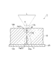
- a modified region is formed in the processing object along the planned cutting line by irradiating the plate-shaped processing object with a laser beam with a focusing point aligned. . Therefore, first, the formation of the modified region in the workpiece cutting method according to the present embodiment will be described with reference to FIGS.
- a laser processing apparatus 100 includes a laser light source 101 that oscillates a laser beam (processing laser beam) L, and a dichroic mirror that is disposed so as to change the direction of the optical axis of the laser beam L by 90 °. 103 and a condensing lens 105 for condensing the laser light L.
- the laser processing apparatus 100 also includes a support 107 for supporting the workpiece 1 irradiated with the laser light L collected by the condensing lens 105, and the support 107 in the X, Y, and Z axis directions.
- the laser light L emitted from the laser light source 101 has its optical axis changed by 90 ° by the dichroic mirror 103, and the inside of the processing object 1 placed on the support base 107.
- the light is condensed by the condenser lens 105.
- the stage 111 is moved, and the workpiece 1 is moved relative to the laser beam L along the planned cutting line 5.
- a modified region serving as a starting point for cutting is formed on the workpiece 1 along the planned cutting line 5.
- the modified region will be described in detail.
- a scheduled cutting line 5 for cutting the workpiece 1 is set on the plate-like workpiece 1.
- the planned cutting line 5 is a virtual line extending linearly.
- the laser beam L is projected along the planned cutting line 5 in a state where the focused point P is aligned with the inside of the workpiece 1. It moves relatively (that is, in the direction of arrow A in FIG. 2).
- the modified region 7 is formed inside the workpiece 1 along the planned cutting line 5, and the modified region 7 formed along the planned cutting line 5 is formed. It becomes the cutting start area 8.
- the condensing point P is a location where the laser light L is condensed.
- the planned cutting line 5 is not limited to a straight line, but may be a curved line, or may be a line actually drawn on the surface 3 of the workpiece 1 without being limited to a virtual line.
- the modified region 7 may be formed continuously or intermittently.
- region 7 should just be formed in the inside of the workpiece 1 at least.
- a crack may be formed starting from the modified region 7, and the crack and modified region 7 may be exposed on the outer surface (front surface, back surface, or outer peripheral surface) of the workpiece 1.
- the laser beam L passes through the workpiece 1 and is particularly absorbed in the vicinity of the condensing point inside the workpiece 1, thereby forming a modified region 7 in the workpiece 1 (internal) Absorption laser processing). Therefore, since the laser beam L is hardly absorbed by the surface 3 of the workpiece 1, the surface 3 of the workpiece 1 is not melted. Generally, when a removed portion such as a hole or a groove is formed by being melted and removed from the front surface 3, the processing region gradually proceeds from the front surface 3 side to the back surface side (surface absorption laser processing).
- the modified region formed by the workpiece cutting method according to the present embodiment refers to a region in which density, refractive index, mechanical strength, and other physical characteristics are different from the surroundings. For example, there are (1) a melt treatment region, (2) a crack region, a dielectric breakdown region, and (3) a refractive index change region, and there are regions where these are mixed.
- the modified region in the workpiece cutting method according to the present embodiment is formed by a phenomenon of local absorption of laser light or multiphoton absorption.
- melt-processed region by multiphoton absorption is described in, for example, “Evaluation of silicon processing characteristics by picosecond pulse laser” on pages 72 to 73 of the 66th Annual Meeting of the Japan Welding Society (April 2000). Are listed.
- a focusing point is set inside a workpiece (for example, a semiconductor material such as silicon), and the electric field intensity at the focusing point is 1 ⁇ 10 8 (W / cm 2 ) or more and the pulse width is 1 ⁇ s or less.
- Laser light L is irradiated. As a result, the laser beam L is absorbed in the vicinity of the condensing point, and the inside of the processing object is locally heated, and a melting treatment region is formed inside the processing object by this heating.
- the melting treatment region is a region once solidified after being melted, a region just in a molten state, a region re-solidified from a molten state, and can also be referred to as a phase-changed region or a region where the crystal structure has changed.
- the melt treatment region can also be said to be a region in which one structure is changed to another structure in a single crystal structure, an amorphous structure, or a polycrystalline structure.
- a region changed from a single crystal structure to an amorphous structure a region changed from a single crystal structure to a polycrystalline structure, or a region changed from a single crystal structure to a structure including an amorphous structure and a polycrystalline structure.
- the melt processing region has, for example, an amorphous silicon structure.
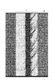
- FIG. 7 is a view showing a photograph of a cross section of a part of a silicon wafer (semiconductor substrate) irradiated with laser light. As shown in FIG. 7, a melt processing region 13 is formed inside the semiconductor substrate 11.
- FIG. 8 is a diagram showing the relationship between the wavelength of the laser beam and the transmittance inside the silicon substrate. However, the reflection components on the front side and the back side of the silicon substrate are removed to show the transmittance only inside. The above relationship was shown for each of the thickness t of the silicon substrate of 50 ⁇ m, 100 ⁇ m, 200 ⁇ m, 500 ⁇ m, and 1000 ⁇ m.
- the thickness of the silicon substrate is 500 ⁇ m or less at the wavelength of 1064 nm of the Nd: YAG laser, it can be seen that the laser light L is transmitted by 80% or more inside the silicon substrate. Since the thickness of the semiconductor substrate 11 shown in FIG. 7 is 350 ⁇ m, the melt processing region 13 is formed near the center of the semiconductor substrate 11, that is, at a portion of 175 ⁇ m from the surface. The transmittance in this case is 90% or more with reference to a silicon wafer having a thickness of 200 ⁇ m, so that the laser light L is hardly absorbed inside the semiconductor substrate 11 and is almost transmitted.
- the laser beam L is condensing the laser beam L inside the silicon wafer under the conditions of 1 ⁇ 10 8 (W / cm 2 ) or more and a pulse width of 1 ⁇ s or less, the laser beam is absorbed locally at and near the focal point. Then, the melt processing region 13 is formed inside the semiconductor substrate 11.
- cracks may occur in the silicon wafer starting from the melt processing region.
- cracks are included in the melt treatment region.
- the cracks are formed over the entire surface in the melt treatment region, or are formed in only a part or a plurality of parts.
- the crack may grow naturally or may grow by applying a force to the silicon wafer.
- the melt processing region is formed inside the silicon wafer, and the melt processing region is formed inside the cut surface as shown in FIG. (2)
- the modified region includes a crack region
- a focusing point is set inside a workpiece (for example, a piezoelectric material made of glass or LiTaO 3 ), and the electric field intensity at the focusing point is 1 ⁇ 10 8 (W / cm 2 ) or more and the pulse width is 1 ⁇ s or less.
- the laser beam L is irradiated under conditions.
- the magnitude of the pulse width is a condition that the laser beam L is absorbed inside the workpiece and a crack region is formed.
- a phenomenon called optical damage occurs inside the workpiece. This optical damage induces thermal strain inside the workpiece, thereby forming a crack region containing one or more cracks inside the workpiece. It can be said that the crack region is a dielectric breakdown region.
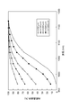
- FIG. 9 is a diagram showing experimental results of the relationship between the electric field strength and the crack size.
- the horizontal axis represents the peak power density. Since the laser beam L is a pulse laser beam, the electric field strength is represented by the peak power density.
- the vertical axis indicates the size of a crack portion (crack spot) formed inside the workpiece by one pulse of laser light L. Crack spots gather to form a crack region. The size of the crack spot is the size of the portion having the maximum length in the shape of the crack spot. Data indicated by black circles in the graph is for the case where the magnification of the condenser lens (C) is 100 times and the numerical aperture (NA) is 0.80.
- the data indicated by the white circles in the graph is when the magnification of the condenser lens (C) is 50 times and the numerical aperture (NA) is 0.55. From the peak power density of about 10 11 (W / cm 2 ), it can be seen that a crack spot is generated inside the workpiece, and the crack spot increases as the peak power density increases. (3) When the modified region includes a refractive index changing region
- the focusing point is set inside the object to be processed (eg, glass), and the laser beam L is irradiated under the condition that the electric field intensity at the focusing point is 1 ⁇ 10 8 (W / cm 2 ) or more and the pulse width is 1 ns or less.
- the laser beam L is absorbed inside the object to be processed in a state where the pulse width is extremely short, the energy is not converted into thermal energy, and the ion valence change, crystallization occurs inside the object to be processed.
- a permanent structural change such as a polarization orientation is induced, and a refractive index change region is formed.
- the modified region includes the melt-processed region, the dielectric breakdown region, the refractive index change region, etc., and the mixed region thereof, and the density of the modified region in the material is compared with the density of the non-modified region. It may be a changed region or a region where lattice defects are formed. These can be collectively referred to as a high-density transition region.
- the area where the density of the melt-processed area, the refractive index changing area, the modified area is changed compared to the density of the non-modified area, and the area where lattice defects are formed are further divided into these areas and the modified area.
- cracks (cracks, microcracks) are included in the interface with the non-modified region.
- the included crack may be formed over the entire surface of the modified region, or may be formed in only a part or a plurality of parts.
- the modified region is formed as follows in consideration of the crystal structure of the object to be processed and its cleavage property, the object to be processed can be accurately cut.
- the orientation flat on the substrate along the direction in which the modified region is to be formed (for example, the direction along the (111) plane in the single crystal silicon substrate) or the direction perpendicular to the direction in which the modified region is to be formed. If this is formed, the modified region can be easily and accurately formed on the substrate by using the orientation flat as a reference.
- FIG. 10 is a plan view of a processing target to which the processing target cutting method according to the first embodiment is applied
- FIG. 11 is a partial cross-section along the planned cutting line of the processing target in FIG. FIG.
- the plate-like workpiece 1 includes a silicon substrate 12.
- a functional element layer (not shown) including a plurality of functional elements is formed on the surface 12a of the workpiece 1 (that is, the surface of the silicon substrate 12).
- the silicon substrate 12 has a single crystal structure, the surface 12a is a (100) plane, and a plane parallel to the orientation flat 6 is a (110) plane.
- the functional element is, for example, a semiconductor operation layer formed by crystal growth, a light receiving element such as a photodiode, a light emitting element such as a laser diode, or a circuit element formed as a circuit.
- the functional element is formed on the orientation flat 6 of the silicon substrate 12. A large number of matrixes are formed in parallel and perpendicular directions.
- the workpiece cutting method according to the first embodiment is applied to the workpiece 1 configured as described above.
- the expanded tape 23 is attached to the surface 12a of the workpiece 1.
- the workpiece 1 is fixed on a support table (not shown) of the laser processing apparatus with the back surface 12b of the workpiece 1 (that is, the back surface of the silicon substrate 12) 12b facing upward.
- the planned cutting lines 5 passing between the adjacent functional elements are set in a lattice shape in a direction perpendicular to the orientation flat 6 and in a parallel direction.
- the back surface 12b of the workpiece 1 is used as the laser light incident surface, and the laser beam L is irradiated with the condensing point P inside the silicon substrate 12, and the orientation is moved by moving the support base.
- the condensing point P is relatively moved along the respective scheduled cutting lines 5 set in a lattice shape in a direction perpendicular to and parallel to the flat 6.
- the relative movement of the condensing point P along each of the scheduled cutting lines 5 is performed a plurality of times with respect to one scheduled cutting line 5, but the distance from the back surface 12b at the position where the focused points P are aligned is determined each time.
- a plurality of rows of modified regions 7 are formed in the silicon substrate 12 one by one with respect to one cutting scheduled line 5 in order from the surface 12a side.
- the wavelength of the laser beam L is 1080 nm or more.
- the transmittance of the silicon substrate 12 is increased. Therefore, the modified region 7 formed by irradiation with the laser beam L is enlarged and formed in the thickness direction of the silicon substrate 12. It is possible to reduce the number of rows in the reforming region 7 and to shorten the tact time.
- the wavelength of the laser beam L is such that the internal transmittance obtained by removing the respective reflection components of the front surface 12a and the back surface 12b of the silicon substrate 12 is 90% or more with respect to the thickness of the silicon substrate 12.
- a dicing apparatus it is not realistic to mount a plurality of laser light sources according to the thickness of the wafer, and a laser capable of precise processing as in the present invention and capable of changing the wavelength according to the thickness of the wafer. There is no light source. Further, the dicing apparatus is required to cut wafers of all thicknesses from thin wafers to thick wafers.
- a laser light source having a wavelength with which the transmittance is 90% or more with reference to a thick wafer.
- a thickness of 300 ⁇ m or more can be considered. Therefore, if the silicon wafer having a thickness of 300 ⁇ m has a transmittance of about 90%, the laser light having a wavelength of 1080 nm or more, and the thickness of the wafer is 500 ⁇ m. It is desirable to apply a laser having a wavelength of 1100 nm or more to the dicing apparatus.
- modified region 7 along the planned cutting line 5 parallel to the orientation flat 6 will be described in more detail.
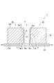
- a plurality of columns (here, four columns) of modified regions (first modified regions) 7a are formed on a silicon substrate with respect to one cutting scheduled line 5.
- One row is formed inside 12, and thereby, a crack (first crack) 17 a is generated from the modified region 7 a to the surface 12 a of the workpiece 1 along the planned cutting line 5.
- a plurality of cutting lines 5 are arranged so that the non-modified region 2 is interposed between the modified region 7a and the modified region 7a on the back surface 12b side of the workpiece 1 with respect to the modified region 7a.
- Rows (here, two rows) of modified regions (second modified regions) 7b are formed one by one inside the silicon substrate 12, so that the unmodified regions 2 are not connected to the cracks 17a. Then, a crack (second crack) 17b is generated from the modified region 7b to the back surface 12b of the workpiece 1 along the planned cutting line 5. At this time, the crack 17 a and the crack 17 b are not connected in the non-modified region 2. That is, the cutting has not been completed, and the workpiece 1 has not been completely cut along the planned cutting line 5.
- the unmodified region 2 is a region having a single crystal structure.
- the modified regions 7a and 7b are regions that have changed from a single crystal structure to an amorphous structure, regions that have changed from a single crystal structure to a polycrystalline structure, or those that have changed from a single crystal structure to an amorphous structure and a polycrystalline structure. Including a melt-processed region which is a region changed to a structure including
- the expanded tape 23 is expanded as shown in FIG.
- a force is applied to the workpiece 1 in the expansion direction, the workpiece 1 is cut into chips starting from the modified region 7, and the semiconductor chip 25 having one functional element is obtained. Many are obtained.
- the expanded tape 23 is in an expanded state, the semiconductor chips 25 are separated from each other.
- the expanded tape 23 is expanded to generate stress on the workpiece 1, thereby causing cracks 17 a in the non-modified region 2. And the crack 17 b are connected, and the workpiece 1 is cut into the semiconductor chip 25 along the cutting scheduled line 5.
- the unmodified region 2 of one cut surface 12c has a thickness direction of the silicon substrate 12.
- a convex portion 18 extending in a substantially orthogonal direction is formed, and a concave portion 19 having a complementary relationship with the convex portion 18 is formed in the non-modified region 2 of the other cut surface 12c.
- the surface 12a of the silicon substrate 12 is the (100) plane and the plane parallel to the orientation flat 6 is the (110) plane, in the planned cutting line 5 parallel to the orientation flat 6,
- the cut surface 12c is a (110) plane.
- the convex portion 18 and the concave portion 19 are each formed in a V-shaped cross section, and the slope forming the convex portion 18 and the concave portion 19 is a (111) plane.
- the crack formed between the modified region 7 and the front surface 12a (or the back surface 12b) is formed in a direction different from the crystal plane, and is not modified between the modified region 7 and the modified region 7.
- a crack is generated (cleaved) in a direction along the crystal plane in a part of the region 2, whereby the wafer is cut.
- a crack 17b is generated on the back surface 12b of the workpiece 1 from the modified region 7b.
- the workpiece 1 is cut by connecting the crack 17a and the crack 17b in the non-modified region 2 by generating stress on the workpiece 1. To do. Thereby, the meandering of the crack etc. in the back surface 12b of the workpiece 1 can be prevented, and the workpiece 1 can be accurately cut along the scheduled cutting line 5.
- the processing object cutting method according to the first embodiment it is possible to reduce the number of columns of the modified regions 7 formed in the thickness direction of the silicon substrate 12 along the planned cutting line 5.
- the plate-like workpiece 1 including the silicon substrate 12 can be accurately cut along the scheduled cutting line 5.
- one of the cut surfaces 12c of the pair of cut surfaces 12c and 12c of the workpiece 1 cut along the scheduled cutting line 5 is not modified.
- a convex portion 18 extending in a direction substantially orthogonal to the thickness direction of the silicon substrate 12 is formed in the mass region 2, and a concave portion 19 corresponding to the convex portion 18 is formed in the non-modified region 2 of the other cut surface 12 c.
- the reformed regions 7a and 7b are formed so as to be formed.
- the surface 12a of the silicon substrate 12 is the (100) surface
- the cutting surface 12c is the (110) surface
- the modified regions 7a and 7b are formed so that becomes the (111) plane.
- the convex part 18 and the recessed part 19 are formed only in the non-modified area 2 interposed between the modified area 7a and the modified area 7b in the cut surface 12c.
- the formation of convex portions 18 and concave portions 19 between the modified regions 7a and 7a adjacent to each other in the thickness direction of the silicon substrate 12 and between the modified regions 7b and 7b adjacent to each other is a reduction in cutting accuracy. It is not preferable in terms.
- the formation of the convex portion 18 or the concave portion 19 between the front surface 12a of the workpiece 1 and the modified region 7a or between the back surface 12b of the workpiece 1 and the modified region 7b is caused by chipping or cracking. It is not preferable in terms of occurrence of
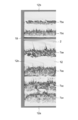
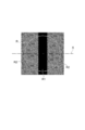
- FIG. 14 is a view showing a photograph of a cut surface of a silicon substrate when a 625 ⁇ m thick silicon substrate is cut starting from the six rows of modified regions.
- a modified region 7a that causes a crack in the surface 12a of the silicon substrate 12 is formed on the cut surface 12c of the silicon substrate 12 so as to be aligned in the thickness direction of the silicon substrate 12 along the planned cutting line. 1 to 7a 4 and modified regions 7b 5 and 7b 6 that cause cracks in the back surface 12b of the silicon substrate 12 are formed.
- a convex portion 18 is formed in the non-modified region 2 between the modified region 7a 4 and the modified region 7b 5 on the cut surface 12c.
- the surface 12a is a (100) plane
- the cut surface 12c is a (110) plane.
- the plane on which the convex portion 18 is formed is a (111) plane.
- the back surface 12b of the silicon substrate 12 is used as a laser light incident surface, and laser light L having a wavelength of 1342 nm is pulse-oscillated with a pulse width of 90 ns and a frequency of 90 kHz. Then, the condensing point P of the laser beam L was moved relative to the silicon substrate 12 along the planned cutting line at a processing speed of 340 mm / s. Thereby, the distance (processing pitch) between the modified spots formed by the irradiation of one pulse of the laser beam L is 3.78 ⁇ m. Other conditions are as shown in Table 1.
- the condensing point position is the distance from the back surface 12b of the silicon substrate 12 that is the laser light incident surface to the position where the condensing point P of the laser light L is aligned
- the width of the modified region is The average value of the width of the modified region in the thickness direction of the silicon substrate 12 (the same applies to Tables 3 and 4 described later).
- the meandering produced on the pair of opposed cut surfaces 12c, 12c was within a maximum of about 3 ⁇ m on the back surface 12b, and the cutting accuracy of the silicon substrate 12 was maintained. Moreover, the bending strength of the chip
- the modified region 7 is enlarged by using the laser beam L having a wavelength of 1342 nm, while the seven modified regions 7 are formed in the thickness direction of the silicon substrate 12 from the surface 12a of the silicon substrate 12. This is because the crack continuously proceeds on the back surface 12b (that is, the connection between the crack 17a and the crack 17b is not broken in the non-modified region 2 as in the above-described embodiment). . Then, when cracks continuously progress from the front surface 12a of the silicon substrate 12 to the back surface 12b, as shown in FIG.
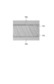
- FIG. 17 is a view showing a photograph of convex portions and concave portions formed in the non-modified region of the cut surface substantially orthogonal to the cut surface of FIG.
- the unmodified region 2 of one cut surface 12 c extends in a direction substantially orthogonal to the thickness direction of the silicon substrate 12.
- a convex portion 18 having a V-shaped cross section is formed, and a concave portion 19 having a V-shaped cross section having a complementary relationship with the convex portion 18 is formed in the non-modified region 2 of the other cut surface 12c.
- FIG. 18 is a schematic diagram showing the convex portion of FIG. As shown in FIG. 18, when the height of the convex portion 18 is X and the width of the convex portion 18 in the thickness direction of the silicon substrate 12 is Y, the results shown in Table 2 are obtained. The angle formed by the inclined surface ((111) surface) forming the convex portion 18 with respect to the cut surface 12c ((110) surface) is 35.3 °.
- the modified regions 7a and 7b so that the height of the convex portion 18 is 2 ⁇ m to 6 ⁇ m and the width of the convex portion 18 in the thickness direction of the silicon substrate 12 is 6 ⁇ m to 17 ⁇ m.
- FIG. 19 is a view showing a photograph of a cut surface of a silicon substrate when a 300 ⁇ m thick silicon substrate is cut starting from three rows of modified regions.
- the modified region 7a that causes cracks in the surface 12a of the silicon substrate 12 is formed on the cut surface 12c of the silicon substrate 12 so as to be aligned in the thickness direction of the silicon substrate 12 along the planned cutting line. 1 and modified regions 7b 2 and 7b 3 that cause cracks in the back surface 12b of the silicon substrate 12 are formed.
- a convex portion 18 is formed in the non-modified region 2 between the modified region 7a 1 and the modified region 7b 2 on the cut surface 12c.
- the surface 12a is a (100) plane
- the cut surface 12c is a (110) plane.
- the plane on which the convex portion 18 is formed is a (111) plane.
- the back surface 12b of the silicon substrate 12 is used as a laser light incident surface
- laser light L having a wavelength of 1342 nm is pulse-oscillated with a pulse width of 90 ns and a frequency of 90 kHz
- silicon The condensing point P of the laser beam L was moved relative to the substrate 12 along the planned cutting line at a processing speed of 340 mm / s. Thereby, the distance (processing pitch) between the modified spots formed by the irradiation of one pulse of the laser beam L is 3.78 ⁇ m.
- Other conditions are as shown in Table 3.
- FIG. 20 is a view showing a photograph of a cut surface of a silicon substrate when a 200 ⁇ m thick silicon substrate is cut starting from three rows of modified regions.
- the modified region 7a that causes the surface 12a of the silicon substrate 12 to crack is formed on the cut surface 12c of the silicon substrate 12 so as to be aligned in the thickness direction of the silicon substrate 12 along the planned cutting line. 1 and modified regions 7b 2 and 7b 3 that cause cracks in the back surface 12b of the silicon substrate 12 are formed.
- a convex portion 18 is formed in the non-modified region 2 between the modified region 7a 1 and the modified region 7b 2 on the cut surface 12c.
- the surface 12a is a (100) plane
- the cut surface 12c is a (110) plane.
- the plane on which the convex portion 18 is formed is a (111) plane.
- the back surface 12b of the silicon substrate 12 is used as a laser light incident surface
- laser light L having a wavelength of 1342 nm is pulse-oscillated with a pulse width of 90 ns and a frequency of 90 kHz
- silicon The condensing point P of the laser beam L was moved relative to the substrate 12 along the planned cutting line at a processing speed of 340 mm / s. Thereby, the distance (processing pitch) between the modified spots formed by the irradiation of one pulse of the laser beam L is 3.78 ⁇ m.
- Other conditions are as shown in Table 4.
- the connection between the crack 17a and the crack 17b was cut, and the silicon substrate 12 could be cut along the planned cutting line with good cutting.
- the silicon substrate 12 is cut when the laser light L having a wavelength of 1064 nm or more is used in order to reduce the number of columns of the modified regions 7 formed in the thickness direction of the silicon substrate 12.
- the width of the non-modified region is the width of the non-modified region 2 in the thickness direction of the silicon substrate 12 (that is, the width of the modified region 7a that causes a crack in the surface 12a of the silicon substrate 12).
- the modified regions 7a and 7b are formed so that the width of the non-modified region 2 in the thickness direction of the silicon substrate 12 is 10% to 30% of the thickness of the silicon substrate 12. Is preferred.
- the modified regions 7a and 7b are formed in this way, when the silicon substrate 12 is cut along the planned cutting line, the meandering cracks and the remaining cracks on the back surface 12b of the silicon substrate 12 are prevented, and the silicon substrate 12 is formed. It is possible to cut accurately and reliably along the scheduled cutting line.
- the present invention is not limited to the first embodiment described above.
- the back surface 12b of the workpiece 1 is a laser light incident surface
- the front surface 12a of the workpiece 1 may be a laser light incident surface.
- FIG. 21 is a plan view of a processing target to which the processing target cutting method according to the second embodiment is applied.
- the plate-like workpiece 1 includes a silicon substrate 11 and a functional element layer 16 formed on the surface 11 a of the silicon substrate 11.
- the functional element layer 16 includes a plurality of functional elements 15 formed in a matrix in a direction parallel to and perpendicular to the orientation flat 6 of the silicon substrate 11.
- the functional element 15 is, for example, a semiconductor operation layer formed by crystal growth, a light receiving element such as a photodiode, a light emitting element such as a laser diode, or a circuit element formed as a circuit.
- the cutting target line 5 is set in a lattice shape on the workpiece 1 so as to pass between the adjacent functional elements 15 and 15.
- the workpiece 1 is cut along the planned cutting line 5, and each cut chip becomes a semiconductor device having one functional element 15.
- FIG. 22 is a configuration diagram of a laser processing apparatus used for carrying out the processing object cutting method according to the second embodiment.
- the laser processing apparatus 300 includes a laser light source 202, a reflective spatial light modulator 203, a 4f optical system 241, and a condensing optical system 204.
- the reflective spatial light modulator 203, the 4f optical system 241 and the condensing optical system 204 are housed in a housing 234, and the laser light source 202 is housed in a housing 231 including the housing 234.
- the laser light source 202 emits laser light L that is pulse laser light having a wavelength of, for example, 1080 nm or more, and for example, a fiber laser is used.
- the laser light source 202 here is fixed to the top plate 236 of the housing 234 with screws or the like so as to emit the laser light L in the horizontal direction.
- the reflective spatial light modulator 203 modulates the laser light L emitted from the laser light source 202.
- LCOS Liquid Crystal Silicon
- SLM Spatial Light Modulator
- the reflective spatial light modulator 203 modulates the laser beam L incident from the horizontal direction while reflecting the laser beam L obliquely upward with respect to the horizontal direction.
- FIG. 23 is a partial cross-sectional view of the reflective spatial light modulator of FIG.
- the reflective spatial light modulator 203 includes a silicon substrate 213, a drive circuit layer 914, a plurality of pixel electrodes 214, a reflective film 215 such as a dielectric multilayer mirror, an alignment film 999a, and a liquid crystal layer 216.
- An alignment film 999b, a transparent conductive film 217, and a transparent substrate 218 such as a glass substrate, which are laminated in this order.
- the transparent substrate 218 has a surface 218 a along the XY plane, and the surface 218 a constitutes the surface of the reflective spatial light modulator 203.
- the transparent substrate 218 mainly contains a light transmissive material such as glass, for example, and the laser light L having a predetermined wavelength incident from the surface 218 a of the reflective spatial light modulator 203 is converted into the interior of the reflective spatial light modulator 203. To penetrate.
- the transparent conductive film 217 is formed on the back surface 218b of the transparent substrate 218, and mainly includes a conductive material (for example, ITO) that transmits the laser light L.
- the plurality of pixel electrodes 214 are two-dimensionally arranged according to the arrangement of the plurality of pixels, and are arranged on the silicon substrate 213 along the transparent conductive film 217.
- Each pixel electrode 214 is made of a metal material such as aluminum, and the surface 214a is processed flat and smooth.
- the plurality of pixel electrodes 214 are driven by an active matrix circuit provided in the drive circuit layer 914.
- the active matrix circuit is provided between the plurality of pixel electrodes 214 and the silicon substrate 213, and controls the voltage applied to each pixel electrode 214 in accordance with the optical image to be output from the reflective spatial light modulator 203.
- Such an active matrix circuit includes, for example, a first driver circuit that controls the applied voltage of each pixel column arranged in the X-axis direction (not shown) and a first driver circuit that controls the applied voltage of each pixel column arranged in the Y-axis direction. And a predetermined voltage is applied to the pixel electrode 214 of the pixel designated by both of the driver circuits by the control unit 250.
- the alignment films 999a and 999b are arranged on both end faces of the liquid crystal layer 216, and the liquid crystal molecule groups are arranged in a certain direction.
- the alignment films 999a and 999b are made of, for example, a polymer material such as polyimide, and the contact surface with the liquid crystal layer 216 is subjected to a rubbing process or the like.
- the liquid crystal layer 216 is disposed between the plurality of pixel electrodes 214 and the transparent conductive film 217, and modulates the laser light L in accordance with an electric field formed by each pixel electrode 214 and the transparent conductive film 217. That is, when a voltage is applied to a certain pixel electrode 214 by the active matrix circuit, an electric field is formed between the transparent conductive film 217 and the pixel electrode 214.
- This electric field is applied to each of the reflective film 215 and the liquid crystal layer 216 at a rate corresponding to the thickness of each. Then, the alignment direction of the liquid crystal molecules 216a changes according to the magnitude of the electric field applied to the liquid crystal layer 216.
- the laser light L passes through the transparent substrate 218 and the transparent conductive film 217 and enters the liquid crystal layer 216, the laser light L is modulated by the liquid crystal molecules 216 a while passing through the liquid crystal layer 216 and reflected by the reflective film 215. Then, the light is again modulated by the liquid crystal layer 216 and taken out.
- the wavefront of the laser light L incident on and transmitted through the modulation pattern (modulation image) is adjusted, and the phase of a component in a predetermined direction orthogonal to the traveling direction of each light beam constituting the laser light L is adjusted. Deviation occurs.
- the 4f optical system 241 adjusts the wavefront shape of the laser light L modulated by the reflective spatial light modulator 203.
- the 4f optical system 241 includes a first lens 241a and a second lens 241b.
- the distance (optical path length) between the reflective spatial light modulator 203 and the first lens 241a is the focal length f1 of the first lens 241a
- the distance (optical path length) between the condensing optical system 204 and the lens 241b .
- f1 focal length of the lens 241a
- f2 focal length of the lens 241b
- the distance (optical path length) between the first lens 241a and the second lens 241b becomes f1 + f2
- the first lens 241a and the second lens 241b become a bilateral telecentric optical system.
- the reflective spatial light modulator 203 and the condensing optical system 204 are disposed. According to the 4f optical system 241, it is possible to suppress an increase in aberration due to a change in the wavefront shape of the laser light L modulated by the reflective spatial light modulator 203 due to spatial propagation.
- the condensing optical system 204 condenses the laser light L modulated by the 4f optical system 241 inside the workpiece 1.
- the condensing optical system 204 includes a plurality of lenses, and is installed on the bottom plate 233 of the housing 234 via a drive unit 232 including a piezoelectric element and the like.
- the laser processing apparatus 300 includes a surface observation unit 211 for observing the surface 3 of the workpiece 1 and an AF (AutoFocus) unit for finely adjusting the distance between the condensing optical system 204 and the workpiece 1. 212 in the housing 231.
- AF AutoFocus
- the surface observation unit 211 includes an observation light source 211a that emits visible light VL1, and a detector 211b that receives and detects the reflected light VL2 of the visible light VL1 reflected by the surface 3 of the workpiece 1. ing.
- the visible light VL1 emitted from the observation light source 211a is reflected and transmitted by the mirror 208 and the dichroic mirrors 209, 210, and 238, and is condensed toward the object to be processed by the condensing optical system 204.
- the reflected light VL2 reflected by the surface 3 of the workpiece 1 is collected by the condensing optical system 204, transmitted and reflected by the dichroic mirrors 238 and 210, and then transmitted through the dichroic mirror 209 to be detected. Light is received at 211b.
- the AF unit 212 emits the AF laser beam LB1 and receives and detects the reflected light LB2 of the AF laser beam LB1 reflected by the surface 3 of the workpiece 1, thereby detecting the surface along the planned cutting line 5 3 displacement data (position (height) data of the surface 3 in the thickness direction of the workpiece 1) is acquired. Then, when forming the modified region 7, the AF unit 212 drives the drive unit 232 based on the acquired displacement data, and moves the condensing optical system 204 along the waviness of the surface 3 of the workpiece 1. Reciprocate in the optical axis direction.
- the laser processing apparatus 300 includes a control unit 250 including a CPU, a ROM, a RAM, and the like as a unit for controlling the laser processing apparatus 300.
- the control unit 250 controls the laser light source 202 and adjusts the output, pulse width, and the like of the laser light L emitted from the laser light source 202.
- the simultaneous focusing position of the laser light L is located at a predetermined distance from the surface 3 of the workpiece 1 and relatively moves along the scheduled cutting line 5.
- the position of the housing 231 and the stage 111 and the drive of the drive unit 232 are controlled.
- control unit 250 applies a predetermined voltage between each pixel electrode 214 and the transparent conductive film 217 in the reflective spatial light modulator 203, and performs predetermined modulation on the liquid crystal layer 216. Display the pattern. Thereby, the laser beam L can be modulated as desired by the reflective spatial light modulator 203.
- the modified region 7 that is the starting point of cutting is cut along the planned cutting line 5 by irradiating the laser beam L with the condensing point P inside the plate-shaped processing target 1.
- the case of forming inside 1 will be described.
- an expand tape is attached to the back surface 21 of the workpiece 1, and the workpiece 1 is placed on the stage 111. Subsequently, the processing object 1 and the laser beam L are relatively moved along the planned cutting line 5 while irradiating the processing object 1 with the laser beam L in a pulsed manner using the surface 3 of the processing object 1 as the laser beam irradiation surface ( Scanning) to form the modified region 7.
- the laser light L emitted from the laser light source 202 travels in the horizontal direction in the housing 231, is reflected downward by the mirror 205 a, and the light intensity is adjusted by the attenuator 207. .
- the laser light L is reflected in the horizontal direction by the mirror 205 b, the intensity distribution is made uniform by the beam homogenizer 260, and is incident on the reflective spatial light modulator 203.
- the laser beam L incident on the reflective spatial light modulator 203 passes through the modulation pattern displayed on the liquid crystal layer 216, is modulated according to the modulation pattern, and then is emitted obliquely upward with respect to the horizontal direction. Subsequently, after the laser beam L is reflected upward by the mirror 206a, the polarization direction is changed by the ⁇ / 2 wavelength plate 228 so that the polarization direction is along the planned cutting line 5, and is reflected by the mirror 206b in the horizontal direction. The light enters the 4f optical system 241.
- the wavefront shape is adjusted so that the laser light L incident on the condensing optical system 204 becomes parallel light.
- the laser light L is transmitted through the first lens 241a and converged, reflected downward by the mirror 219, and diverges through the confocal O.
- the diverged laser light L passes through the second lens 241b and is converged again so as to become parallel light.
- the laser light L sequentially passes through the dichroic mirrors 210 and 218 and enters the condensing optical system 204, and is condensed by the condensing optical system 204 inside the workpiece 1 placed on the stage 111. Is done. As a result, a modified spot is formed at a predetermined depth in the thickness direction in the workpiece 1.
- the condensing point P of the laser beam L is relatively moved along the planned cutting line 5, and the modified region 7 is formed by a plurality of modified spots.
- the expanded tape is expanded to cut the workpiece 1 along the planned cutting line 5 using the modified region 7 as a starting point of cutting, and the plurality of cut chips are replaced with a semiconductor device (for example, memory, IC, light emission). Element, light receiving element, etc.).
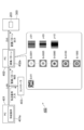
- the laser processing system 400 includes personal computers (hereinafter referred to as “PCs”) 401 and 402, a controller 403, and a laser processing apparatus 300.
- PCs personal computers
- the laser processing apparatus 300 irradiates the workpiece 1 with the laser light L modulated by the reflective spatial light modulator 203 to form the modified region 7 in the workpiece 1. .
- the formation conditions of the modified region 7 for the workpiece 1 are stored as a database.
- the formation condition is input to the controller 403 via a LAN (Local Area Network).
- the controller (pattern designating unit) 403 selects one or more element patterns for the modified region 7 according to the formation condition. Then, the element pattern is designated to the PC 402 via the LAN.
- the element pattern is a pattern serving as an element of a modulation pattern for performing predetermined modulation on the laser light L in the reflective spatial light modulator 203 of the laser processing apparatus 300, and a plurality of types of element patterns are included in the PC 402. It is stored as a database in a storage unit (memory, hard disk, etc.) 402a.
- the storage unit (pattern storage unit) 402a is an individual difference correction pattern (D-01) for correcting individual differences occurring in the laser processing apparatus 300 (for example, distortion occurring in the liquid crystal layer 216 of the reflective spatial light modulator 203). Is stored as an element pattern. Further, the storage unit 402a stores, as element patterns, spherical aberration correction patterns (S-0001 to S-1000) for correcting spherical aberration generated at the condensing point P of the laser light L.
- the spherical aberration correction pattern is set with the material and the distance as parameters, and is stored in the storage unit 402a.
- the storage unit 402a stores quality patterns (J-01 to J-10) as element patterns.
- the quality pattern includes the first brightness region R1 extending in a direction substantially orthogonal to the planned cutting line 5 and both sides of the first brightness region R1 in the extending direction of the planned cutting line 5.
- the quality pattern has a position on the back surface 21 side, a position on the back surface 21 side of the processing object 1, a position on the surface 3 side of the processing object 1, and an intermediate position between the position on the back surface 21 side and the position on the front surface 3 side.
- the modified region 7 is formed in the order of the position, the intermediate position, and the position on the front surface 3 side (or in the order of the position on the front surface 3 side, the intermediate position, and the position on the back surface 21 side), the modified region is formed at the intermediate position. Used when forming 7.
- the quality pattern is formed after the modified region 7 is formed at the position on the back surface 21 side and before the modified region 7 is formed at the position on the front surface 3 side (or the modified region 7 is formed at the position on the front surface 3 side. This is used when the modified region 7 is formed at an intermediate position after the formation and before the modified region 7 is formed at the position on the back surface 21 side.
- the formation of the modified region 7 at the position on the back surface 21 side means that the center of the modified region 7 is located on the back surface 21 side of the workpiece 1 from the center position of the workpiece 1 in the thickness direction of the workpiece 1. It means that the modified region 7 is formed so that the position is deviated, and forming the modified region 7 at the position on the surface 3 side means that the center of the workpiece 1 is in the thickness direction of the workpiece 1. This means that the modified region 7 is formed so that the center position of the modified region 7 is deviated from the position toward the surface 3 of the workpiece 1.
- the formation of the modified region 7 at an intermediate position between the position on the back surface 21 side and the position on the front surface 3 side means that the modified region 7 is formed at a position on the back surface 21 side and a position on the front surface 3 side.
- a trait region is formed with the modified region 7 to be processed (that is, the center position of the modified region 7 coincides with the center position of the workpiece 1 in the thickness direction of the workpiece 1). Thus, it does not mean that the modified region 7 is formed).
- the PC (pattern creation means) 402 reads one or more types of element patterns from the storage unit 402a for the modified region 7 based on the designation of the element patterns by the controller 403. That is, the PC 402 acquires one or more types of element patterns for the modified region 7 from the storage unit 402 a in accordance with the formation conditions of the modified region 7 for the workpiece 1.
- the PC 402 When the PC 402 acquires a kind of element pattern, the PC 402 sets the kind of element pattern as a modulation pattern in order to form the corresponding modified region 7. In addition, when the PC 402 acquires a plurality of types of element patterns, the PC 402 uses a combined pattern obtained by combining the plurality of types of element patterns as a modulation pattern in order to form the corresponding modified region 7. After creating the modulation pattern in this way, the PC 402 associates the modulation pattern with the modified region 7 and outputs the modulation pattern to the laser processing apparatus 300 via DVI (Digital Visual Interface).
- DVI Digital Visual Interface
- the PC 402 creates a modulation pattern for each modified region 7 for all types of modified regions 7, and then associates the modulation pattern with each modified region 7 and laser processing apparatus 300. Output to.
- the width of the first brightness region R1 is 20% of the width of the effective region R for modulating the laser light L in the modulation pattern.
- the ratio is ⁇ 50%.
- the width of the first brightness region R1 may be narrower than the width of each of the second brightness regions R2 (for example, J-01 in FIG. 24). Or may be wider than each width of the second brightness region R2 (see, for example, J-10 in FIG. 24).
- the effective area R of the quality pattern is an area corresponding to an amount of the laser light L incident on the condensing optical system 204 (an amount incident on the entrance pupil of the condensing optical system 204).
- the average brightness of the first brightness region R1 and the average brightness of the second brightness region R2 are different from each other, either one may be brighter.
- the first lightness region R1 Preferably, the average brightness of the second brightness area R2 is shifted by 128 gradations.
- the user operates the PC 401 to input conditions for forming the modified region 7 on the workpiece 1 (step S11).
- the thickness of the workpiece 1 is set to 300 ⁇ m
- the material of the workpiece 1 is set to silicon.
- three rows of modified regions SD1, SD2, SD3 are set as a plurality of rows of modified regions 7 formed so as to be aligned in the thickness direction of the workpiece 1 with respect to one scheduled cutting line 5. Has been.
- the distance (depth) from the laser light incident surface of the workpiece 1 to the condensing point P of the laser light L is set to 260 ⁇ m, and the output of the laser light L is 0. It is set to 6W.
- the distance is set to 180 ⁇ m, and the output is set to 0.6W.
- the distance is set to 70 ⁇ m and the output is set to 0.6W.
- the quality pattern is set to “Yes”.
- the modified region SD1 corresponds to the modified region 7b in which the crack 17b is generated from the modified region to the back surface 21 of the workpiece 1 at the time of forming the modified region, and the modified region SD3 is modified.
- This corresponds to the modified region 7a in which a crack 17a is generated from the modified region to the surface 3 of the workpiece 1 at the time of formation of the quality region. Therefore, this specific example of the second embodiment is that the modified region SD2 is formed in the non-modified region 2 interposed between the modified region SD1 and the modified region SD3. Different from the second embodiment.
- the controller 403 determines one or more elements for each of the modified regions SD1, SD2, SD3 according to the formation conditions. A pattern is selected, and the element pattern is specified for the PC 402 in association with each of the reforming areas SD1, SD2, and SD3 (step S12). Thereby, it is possible to cause the PC 402 to acquire an appropriate element pattern easily and reliably.
- the PC 402 selects the corresponding element pattern from the storage unit 402a in association with each of the reforming regions SD1, SD2, and SD3 (step S13).
- the individual difference correction pattern D-01 and the spherical aberration correction pattern S-0025 are selected as element patterns in association with the modified region SD3.
- the individual difference correction pattern D-01, the spherical aberration correction pattern S-0060, and the quality pattern J-03 are selected as element patterns in association with the modified region SD2.
- the individual difference correction pattern D-01 and the spherical aberration correction pattern S-0100 are selected as element patterns in association with the modified region SD1.
- the PC 402 synthesizes a plurality of types of element patterns associated with the reforming regions SD1, SD2, and SD3 to form the reforming regions SD1, SD2, and SD3, and the synthesized pattern is used as a modulation pattern.
- Step S14 the individual difference correction pattern D-01 and the spherical aberration correction pattern S-0025 are combined to create a modulation pattern SD-003.
- the individual difference correction pattern D-01, the spherical aberration correction pattern S-0060, and the quality pattern J-03 are combined to create a modulation pattern SD-002.
- the individual difference correction pattern D-01 and the spherical aberration correction pattern S-0100 are combined to create a modulation pattern SD-001.
- the PC 402 associates the created modulation patterns SD-001, SD-002, and SD-003 with each of the modified regions SD1, SD2, and SD3 and outputs them to the laser processing apparatus 300 (step S15).
- the laser processing apparatus 300 performs laser processing (step S16).
- the modulation pattern SD-001 is displayed on the liquid crystal layer 216 of the reflective spatial light modulator 203 via the control unit 250.
- the laser beam L is modulated by the modulation pattern SD-001.
- the modulation pattern SD-002 is displayed on the liquid crystal layer 216 of the reflective spatial light modulator 203 via the control unit 250, and the laser beam L is emitted by the modulation pattern SD-002. Modulated.
- the modulation pattern SD-003 is displayed on the liquid crystal layer 216 of the reflective spatial light modulator 203 via the controller 250, and the laser beam L is emitted by the modulation pattern SD-003. Modulated.
- the modulation pattern includes the individual difference correction pattern and the spherical aberration correction pattern. Variations in the formation state of the modified region due to spherical aberration occurring at the light spot P can be suppressed.
- the modified region SD1 at a position far from the laser light incident surface of the workpiece 1, the modified region SD2 positioned at the middle, and the modified region SD3 at a position near the laser light incident surface of the workpiece 1 are sequentially formed. It is desirable.
- the modulation pattern includes an individual difference correction pattern and a spherical surface.
- a quality pattern is included in addition to the aberration correction pattern.
- the modified region SD3 at a position near the laser beam incident surface of the workpiece 1 is sequentially formed with the modified region SD2 positioned at the middle, and the modified region SD1 at a position far from the laser beam incident surface of the workpiece 1. May be.
- FIG. 27 is a first diagram illustrating a cut surface when a workpiece is cut starting from the modified region.
- the modified regions SD1 to SD5 were formed in order from the surface 3 with the surface 3 of the workpiece 1 made of silicon having a thickness of 400 ⁇ m as the laser light incident surface.
- the spherical aberration is corrected at the condensing point P of the laser beam L, respectively.
- the possible spherical aberration correction pattern S was used, and the laser light L was modulated with a modulation pattern including the spherical aberration correction pattern S in addition to the individual difference correction pattern D. Further, when forming the modified region SD3 at an intermediate position between the position on the back surface 21 side and the position on the front surface 3 side, the modulation pattern including the quality pattern J in addition to the individual difference correction pattern D and the spherical aberration correction pattern S. Then, the laser beam L was modulated.
- the modified regions SD1 and SD2 correspond to the modified region 7b in which the crack 17b is generated from the modified region to the back surface 21 of the workpiece 1 at the time of forming the modified region.
- SD5 corresponds to a modified region 7a in which a crack 17a is generated from the modified region to the surface 3 of the workpiece 1 at the time of forming the modified region. Therefore, the specific example of the second embodiment is that the modified region SD3 is formed in the non-modified region 2 interposed between the modified regions SD1 and SD2 and the modified regions SD4 and SD5. This is different from the second embodiment described above.
- the crack that occurred when the modified regions SD1 and SD2 were formed reached the back surface 21 of the workpiece 1, while it did not connect with the crack that occurred when the modified region SD3 was formed.
- the crack that occurred when the modified regions SD4 and SD5 were formed reached the surface 3 of the workpiece 1 and was not connected to the crack that occurred when the modified region SD3 was formed. Accordingly, it is possible to reduce the number of the modified regions 7 formed in the thickness direction of the workpiece 1 along the planned cutting line 5 while preventing the cutting accuracy of the workpiece 1 from being lowered. It was.
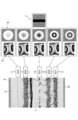
- FIG. 28 is a schematic diagram of a focused spot of laser light for forming a modified region.
- the focused spot CS1 of the laser beam L becomes a circular region as shown in FIG.
- a plurality of condensing spots CS2 of the laser beam L are obtained as shown in FIG.
- These dot-like regions were formed in parallel along the extending direction A (that is, the relative movement direction of the laser beam L) A of the planned cutting line 5.
- region had the case where a part overlaps, and the case where it separated
- the first brightness region R1 extending in a direction substantially orthogonal to the planned cutting line 5 and the second brightness region R2 located on both sides of the first brightness region R1 in the extending direction of the planned cutting line 5.
- the laser beam L is diffracted in the reflective spatial light modulator 203 by the quality pattern having When the laser beam L having such a condensing spot CS2 is irradiated, cracks are continuously generated in the thickness direction of the workpiece 1 when a plurality of modified regions 7 are formed in the thickness direction of the workpiece 1. It is possible to form the modified region 7 in the workpiece 1 that can prevent the process from proceeding.
- the machining target 1 is modified to an intermediate position between the position on the back surface 21 side and the position on the front surface 3 side.
- the first brightness region R1 extending in the direction substantially orthogonal to the planned cutting line 5 and the first brightness region R1 in the extending direction of the planned cutting line 5
- a quality pattern having a second brightness region R2 located on both sides of the image is used. That is, after the modified region 7 is formed at the position on the back surface 21 side and the modified region 7 is formed at the position on the surface 3 side with the front surface 3 as the laser beam incident surface (or the back surface 21 is incident on the laser beam).
- Reflective spatial light modulator based on the modulation pattern including the quality pattern after forming the modified region 7 at the position on the front surface 3 side and before forming the modified region 7 at the position on the back surface 21 side
- the modified region 7 is formed at the intermediate position. Even if the laser beam L having a wavelength longer than 1064 nm is used to reduce the number of rows in the modified region 7 by forming the modified region 7 in the intermediate position in this way, the thickness of the workpiece 1 is increased. It is possible to prevent the cracks from continuously progressing in the thickness direction of the workpiece 1 when forming a plurality of the modified regions 7 in the direction.
- the width of the first brightness region R1 is 20% to the width of the effective region R for modulating the laser light L in the modulation pattern in the extending direction of the planned cutting line 5.
- the ratio is preferably 50%.
- the width of the first lightness region R1 may be narrower than the width of each of the second lightness regions R2, or the width of the second lightness region R2 It may be wider than each width.
- the laser beam L is modulated by the reflective spatial light modulator 203 based on the modulation pattern including the quality pattern, the individual difference correction pattern, and the spherical aberration correction pattern, and the back surface
- the laser beam L is modulated by the reflective spatial light modulator 203 based on the modulation pattern including the individual difference correction pattern and the spherical aberration correction pattern. It is preferable to do.
- the thickness of the workpiece 1 along the planned cutting line 5 The number of rows of the modified regions 7 formed in the direction can be more reliably reduced.
- the wavelength of the laser beam L is preferably 1080 nm or more.
- the modified region 7 formed at the intermediate position, the position on the back surface 21 side, and the position on the front surface 3 side is likely to generate cracks.
- the number of the modified regions 7 formed in the thickness direction of the workpiece 1 along the planned cutting line 5 can be more reliably reduced.
- the workpiece 1 can be cut along the scheduled cutting line 5 with high accuracy by cutting the workpiece 1 along the scheduled cutting line 5 starting from the modified region 7 described above. And a semiconductor device with high reliability can be obtained by manufacturing the semiconductor device by cutting the workpiece 1.
- the number of columns of the modified region 7 (corresponding to the modified region 7b of the first embodiment) formed at the position on the back surface 21 side, the surface 3
- the number of columns of the modified region 7 (corresponding to the modified region 7a of the first embodiment) formed at the position on the side, and the modified region 7 (non-modified of the first embodiment) formed at the intermediate position
- the number of columns of the modified region formed in the mass region 2 can be changed according to the thickness and material of the workpiece 1.
- the number of rows of the modified region 7 formed at the position on the back surface 21 side can be determined so that a crack may occur from the modified region 7 to the back surface 21, and the modified region formed at the position on the front surface 3 side.
- the number of rows in the region 7 can be determined so that a crack can occur in the surface 3 from the modified region 7. Further, the number of the modified regions 7 formed at the intermediate position is such that cracks are continuously formed in the thickness direction of the workpiece 1 when a plurality of the modified regions 7 are formed in the thickness direction of the workpiece 1. It can be determined so that it can be prevented from proceeding to.
- astigmatism correction for correcting astigmatism at the condensing point P of the laser light L as an element pattern serving as an element of the modulation pattern A pattern or the like may be used.
- the spatial light modulator is not limited to the LCOS-SLM, but may be a MEMS-SLM, a DMD (deformable mirror device), or the like. Furthermore, the spatial light modulator is not limited to the reflective type, and may be a transmissive type. Examples of the spatial light modulator include a liquid crystal cell type and an LCD type. Further, in the reflective spatial light modulator 203, the reflection of the pixel electrode of the silicon substrate may be used instead of the dielectric multilayer mirror.
- the number of rows of modified regions formed in the thickness direction of the silicon substrate along the planned cutting line can be reduced, and a plate-like workpiece including the silicon substrate can be accurately cut along the planned cutting line. be able to.
- SYMBOLS 1 Processing object, 5 ... Planned cutting line, 7 ... Modified area
Abstract
Priority Applications (6)
| Application Number | Priority Date | Filing Date | Title |
|---|---|---|---|
| US13/148,097 US8728914B2 (en) | 2009-02-09 | 2010-01-27 | Workpiece cutting method |
| EP10738446.3A EP2394775B1 (fr) | 2009-02-09 | 2010-01-27 | Procédé de découpe d'une pièce |
| JP2010549442A JP5632751B2 (ja) | 2009-02-09 | 2010-01-27 | 加工対象物切断方法 |
| KR1020117016984A KR101757937B1 (ko) | 2009-02-09 | 2010-01-27 | 가공대상물 절단방법 |
| CN201080007011.2A CN102307699B (zh) | 2009-02-09 | 2010-01-27 | 加工对象物的切断方法 |
| US14/256,370 US8865568B2 (en) | 2009-02-09 | 2014-04-18 | Workpiece cutting method |
Applications Claiming Priority (2)
| Application Number | Priority Date | Filing Date | Title |
|---|---|---|---|
| JP2009-027263 | 2009-02-09 | ||
| JP2009027263 | 2009-02-09 |
Related Child Applications (2)
| Application Number | Title | Priority Date | Filing Date |
|---|---|---|---|
| US13/148,097 A-371-Of-International US8728914B2 (en) | 2009-02-09 | 2010-01-27 | Workpiece cutting method |
| US14/256,370 Continuation US8865568B2 (en) | 2009-02-09 | 2014-04-18 | Workpiece cutting method |
Publications (1)
| Publication Number | Publication Date |
|---|---|
| WO2010090111A1 true WO2010090111A1 (fr) | 2010-08-12 |
Family
ID=42542011
Family Applications (1)
| Application Number | Title | Priority Date | Filing Date |
|---|---|---|---|
| PCT/JP2010/051047 WO2010090111A1 (fr) | 2009-02-09 | 2010-01-27 | Procédé de découpe d'une pièce |
Country Status (7)
| Country | Link |
|---|---|
| US (2) | US8728914B2 (fr) |
| EP (1) | EP2394775B1 (fr) |
| JP (1) | JP5632751B2 (fr) |
| KR (1) | KR101757937B1 (fr) |
| CN (1) | CN102307699B (fr) |
| TW (1) | TWI542431B (fr) |
| WO (1) | WO2010090111A1 (fr) |
Cited By (23)
| Publication number | Priority date | Publication date | Assignee | Title |
|---|---|---|---|---|
| JP2012109358A (ja) * | 2010-11-16 | 2012-06-07 | Tokyo Seimitsu Co Ltd | 半導体基板の切断方法及び半導体基板の切断装置 |
| JP2012130952A (ja) * | 2010-12-22 | 2012-07-12 | Hamamatsu Photonics Kk | レーザ加工方法 |
| JP2013065752A (ja) * | 2011-09-20 | 2013-04-11 | Fuji Electric Co Ltd | 半導体装置及びその製造方法 |
| JPWO2011096353A1 (ja) * | 2010-02-05 | 2013-06-10 | 株式会社フジクラ | 微細構造の形成方法および微細構造を有する基体 |
| JP2013126682A (ja) * | 2011-11-18 | 2013-06-27 | Hamamatsu Photonics Kk | レーザ加工方法 |
| WO2014025026A1 (fr) * | 2012-08-10 | 2014-02-13 | 浜松ホトニクス株式会社 | Procédé de fabrication d'élément de diffusion raman exaltée de surface |
| JPWO2012063348A1 (ja) * | 2010-11-11 | 2014-05-12 | パイオニア株式会社 | レーザ加工方法及び装置 |
| JP2016072276A (ja) * | 2014-09-26 | 2016-05-09 | 株式会社ディスコ | ウエーハの加工方法 |
| JP2016072275A (ja) * | 2014-09-26 | 2016-05-09 | 株式会社ディスコ | ウエーハの加工方法 |
| US9588049B2 (en) | 2012-08-10 | 2017-03-07 | Hamamatsu Photonics K.K. | Surface-enhanced Raman scattering unit, and method for using same |
| US9612201B2 (en) | 2012-08-10 | 2017-04-04 | Hamamatsu Photonics K.K. | Surface-enhanced raman scattering element |
| US9726608B2 (en) | 2012-08-10 | 2017-08-08 | Hamamatsu Photonics K.K. | Surface-enhanced raman scattering element |
| US9846123B2 (en) | 2012-08-10 | 2017-12-19 | Hamamatsu Photonics K.K. | Surface-enhanced Raman scattering element |
| US9857306B2 (en) | 2012-08-10 | 2018-01-02 | Hamamatsu Photonics K.K. | Surface-enhanced Raman scattering element |
| US9863884B2 (en) | 2012-08-10 | 2018-01-09 | Hamamatsu Photonics K.K. | Surface-enhanced Raman scattering element, and method for producing same |
| US9863883B2 (en) | 2012-08-10 | 2018-01-09 | Hamamatsu Photonics K.K. | Surface-enhanced raman scattering element |
| US9874523B2 (en) | 2012-08-10 | 2018-01-23 | Hamamatsu Photonics K.K. | Surface-enhanced Raman scattering element including a conductor layer having a base part and a plurality of protusions |
| CN107924830A (zh) * | 2015-08-18 | 2018-04-17 | 浜松光子学株式会社 | 加工对象物切断方法和加工对象物切断装置 |
| CN107995996A (zh) * | 2015-08-18 | 2018-05-04 | 浜松光子学株式会社 | 激光加工装置及激光加工方法 |
| US9976961B2 (en) | 2012-08-10 | 2018-05-22 | Hamamatsu Photonics K.K. | Surface-enhanced raman scattering element including a conductor layer having a base part and a plurality of protusions |
| US10132755B2 (en) | 2012-08-10 | 2018-11-20 | Hamamatsu Photonics K.K. | Surface-enhanced Raman scattering element, and method for manufacturing surface-enhanced Raman scattering element |
| US10408761B2 (en) | 2012-08-10 | 2019-09-10 | Hamamatsu Photonics K.K. | Surface-enhanced Raman scattering element |
| US10551322B2 (en) | 2012-08-10 | 2020-02-04 | Hamamatsu Photonics K.K. | Surface-enhanced Raman scattering unit including integrally formed handling board |
Families Citing this family (46)
| Publication number | Priority date | Publication date | Assignee | Title |
|---|---|---|---|---|
| JP5479924B2 (ja) * | 2010-01-27 | 2014-04-23 | 浜松ホトニクス株式会社 | レーザ加工方法 |
| DE102010009015A1 (de) * | 2010-02-24 | 2011-08-25 | OSRAM Opto Semiconductors GmbH, 93055 | Verfahren zum Herstellen einer Mehrzahl von optoelektronischen Halbleiterchips |
| US20130161797A1 (en) * | 2010-03-05 | 2013-06-27 | Disco Corporation | Single crystal substrate, manufacturing method for single crystal substrate, manufacturing method for single crystal substrate with multilayer film, and element manufacturing method |
| JP2011201759A (ja) * | 2010-03-05 | 2011-10-13 | Namiki Precision Jewel Co Ltd | 多層膜付き単結晶基板、多層膜付き単結晶基板の製造方法および素子製造方法 |
| JP5480169B2 (ja) * | 2011-01-13 | 2014-04-23 | 浜松ホトニクス株式会社 | レーザ加工方法 |
| JP6047874B2 (ja) * | 2011-12-06 | 2016-12-21 | 三菱電機株式会社 | 半導体装置の製造方法 |
| US9499921B2 (en) | 2012-07-30 | 2016-11-22 | Rayton Solar Inc. | Float zone silicon wafer manufacturing system and related process |
| US9404198B2 (en) * | 2012-07-30 | 2016-08-02 | Rayton Solar Inc. | Processes and apparatuses for manufacturing wafers |
| KR101976134B1 (ko) * | 2012-09-12 | 2019-05-08 | 삼성디스플레이 주식회사 | 유기 발광 표시 장치의 제조 방법 |
| JP6127526B2 (ja) * | 2012-10-29 | 2017-05-17 | 三星ダイヤモンド工業株式会社 | レーザー加工装置、および、パターン付き基板の加工条件設定方法 |
| KR101423497B1 (ko) * | 2012-11-22 | 2014-07-29 | 한국기계연구원 | 웨이퍼 다이싱용 레이저 가공장치 및 이를 이용한 웨이퍼 다이싱 방법 |
| JP6423135B2 (ja) * | 2012-11-29 | 2018-11-14 | 三星ダイヤモンド工業株式会社 | パターン付き基板の分割方法 |
| EP2754524B1 (fr) | 2013-01-15 | 2015-11-25 | Corning Laser Technologies GmbH | Procédé et dispositif destinés au traitement basé sur laser de substrats plats, galette ou élément en verre, utilisant un faisceau laser en ligne |
| TWI598174B (zh) * | 2013-01-25 | 2017-09-11 | 鴻海精密工業股份有限公司 | 藍寶石切割裝置 |
| EP2781296B1 (fr) | 2013-03-21 | 2020-10-21 | Corning Laser Technologies GmbH | Dispositif et procédé de découpe de contours à partir de substrats plats au moyen d'un laser |
| KR102215918B1 (ko) * | 2013-03-27 | 2021-02-16 | 하마마츠 포토닉스 가부시키가이샤 | 레이저 가공 장치 및 레이저 가공 방법 |
| CN105209219B (zh) * | 2013-03-27 | 2017-05-17 | 浜松光子学株式会社 | 激光加工装置及激光加工方法 |
| JP6382797B2 (ja) * | 2013-03-27 | 2018-08-29 | 浜松ホトニクス株式会社 | レーザ加工装置及びレーザ加工方法 |
| WO2014156689A1 (fr) | 2013-03-27 | 2014-10-02 | 浜松ホトニクス株式会社 | Dispositif d'usinage laser et procédé d'usinage laser |
| US11556039B2 (en) | 2013-12-17 | 2023-01-17 | Corning Incorporated | Electrochromic coated glass articles and methods for laser processing the same |
| US9517963B2 (en) | 2013-12-17 | 2016-12-13 | Corning Incorporated | Method for rapid laser drilling of holes in glass and products made therefrom |
| JP6258787B2 (ja) | 2014-05-29 | 2018-01-10 | 浜松ホトニクス株式会社 | レーザ加工装置及びレーザ加工方法 |
| US9165832B1 (en) * | 2014-06-30 | 2015-10-20 | Applied Materials, Inc. | Method of die singulation using laser ablation and induction of internal defects with a laser |
| TWI730945B (zh) | 2014-07-08 | 2021-06-21 | 美商康寧公司 | 用於雷射處理材料的方法與設備 |
| EP3552753A3 (fr) | 2014-07-14 | 2019-12-11 | Corning Incorporated | Système et procédé de traitement de matériaux transparents utilisant des lignes focales de faisceau laser réglables en longueur et en diamètre |
| US9859162B2 (en) | 2014-09-11 | 2018-01-02 | Alta Devices, Inc. | Perforation of films for separation |
| JP2016072277A (ja) * | 2014-09-26 | 2016-05-09 | 株式会社ディスコ | ウエーハの加工方法 |
| JP2016143766A (ja) * | 2015-02-02 | 2016-08-08 | 株式会社ディスコ | 単結晶部材の加工方法 |
| GB201502149D0 (en) * | 2015-02-09 | 2015-03-25 | Spi Lasers Uk Ltd | Apparatus and method for laser welding |
| JP7292006B2 (ja) | 2015-03-24 | 2023-06-16 | コーニング インコーポレイテッド | ディスプレイガラス組成物のレーザ切断及び加工 |
| JP6542630B2 (ja) * | 2015-09-29 | 2019-07-10 | 浜松ホトニクス株式会社 | レーザ加工方法及びレーザ加工装置 |
| JP6605278B2 (ja) * | 2015-09-29 | 2019-11-13 | 浜松ホトニクス株式会社 | レーザ加工方法 |
| JP6605277B2 (ja) * | 2015-09-29 | 2019-11-13 | 浜松ホトニクス株式会社 | レーザ加工方法及びレーザ加工装置 |
| CN106881531A (zh) * | 2015-12-10 | 2017-06-23 | 彭翔 | 用于切割脆硬材料的方法和系统 |
| JP6689631B2 (ja) * | 2016-03-10 | 2020-04-28 | 浜松ホトニクス株式会社 | レーザ光照射装置及びレーザ光照射方法 |
| KR102078294B1 (ko) | 2016-09-30 | 2020-02-17 | 코닝 인코포레이티드 | 비-축대칭 빔 스폿을 이용하여 투명 워크피스를 레이저 가공하기 위한 기기 및 방법 |
| US11542190B2 (en) | 2016-10-24 | 2023-01-03 | Corning Incorporated | Substrate processing station for laser-based machining of sheet-like glass substrates |
| JP2018182141A (ja) * | 2017-04-17 | 2018-11-15 | 浜松ホトニクス株式会社 | 加工対象物切断方法 |
| JP7105058B2 (ja) * | 2017-12-05 | 2022-07-22 | 株式会社ディスコ | ウェーハの加工方法 |
| JP7088761B2 (ja) * | 2018-07-05 | 2022-06-21 | 浜松ホトニクス株式会社 | レーザ加工装置 |
| CN115020216A (zh) | 2018-11-01 | 2022-09-06 | 精材科技股份有限公司 | 晶片封装体的制造方法 |
| US11024501B2 (en) | 2018-12-29 | 2021-06-01 | Cree, Inc. | Carrier-assisted method for parting crystalline material along laser damage region |
| US10562130B1 (en) | 2018-12-29 | 2020-02-18 | Cree, Inc. | Laser-assisted method for parting crystalline material |
| US10576585B1 (en) | 2018-12-29 | 2020-03-03 | Cree, Inc. | Laser-assisted method for parting crystalline material |
| US10611052B1 (en) | 2019-05-17 | 2020-04-07 | Cree, Inc. | Silicon carbide wafers with relaxed positive bow and related methods |
| JP2022097232A (ja) * | 2020-12-18 | 2022-06-30 | 株式会社ディスコ | レーザー加工装置 |
Citations (5)
| Publication number | Priority date | Publication date | Assignee | Title |
|---|---|---|---|---|
| JP2006108459A (ja) | 2004-10-07 | 2006-04-20 | Disco Abrasive Syst Ltd | シリコンウエーハのレーザー加工方法およびレーザー加工装置 |
| JP2006135355A (ja) * | 2002-03-12 | 2006-05-25 | Hamamatsu Photonics Kk | 半導体基板の切断方法 |
| JP2006167804A (ja) * | 2004-11-19 | 2006-06-29 | Canon Inc | レーザ割断方法およびレーザ割断装置 |
| JP2007245173A (ja) * | 2006-03-14 | 2007-09-27 | Hamamatsu Photonics Kk | レーザ加工方法及びレーザ加工装置 |
| JP2009010105A (ja) * | 2007-06-27 | 2009-01-15 | Disco Abrasive Syst Ltd | ウェーハのレーザ加工方法 |
Family Cites Families (53)
| Publication number | Priority date | Publication date | Assignee | Title |
|---|---|---|---|---|
| US4546231A (en) | 1983-11-14 | 1985-10-08 | Group Ii Manufacturing Ltd. | Creation of a parting zone in a crystal structure |
| KR0171947B1 (ko) | 1995-12-08 | 1999-03-20 | 김주용 | 반도체소자 제조를 위한 노광 방법 및 그를 이용한 노광장치 |
| JP4659300B2 (ja) | 2000-09-13 | 2011-03-30 | 浜松ホトニクス株式会社 | レーザ加工方法及び半導体チップの製造方法 |
| DE60335538D1 (de) | 2002-03-12 | 2011-02-10 | Hamamatsu Photonics Kk | Verfahren zum schneiden eines bearbeiteten objekts |
| TWI326626B (en) | 2002-03-12 | 2010-07-01 | Hamamatsu Photonics Kk | Laser processing method |
| ES2377521T3 (es) | 2002-03-12 | 2012-03-28 | Hamamatsu Photonics K.K. | Método para dividir un sustrato |
| TWI520269B (zh) | 2002-12-03 | 2016-02-01 | Hamamatsu Photonics Kk | Cutting method of semiconductor substrate |
| CN100445014C (zh) | 2002-12-05 | 2008-12-24 | 浜松光子学株式会社 | 激光加工装置 |
| JP2004188422A (ja) | 2002-12-06 | 2004-07-08 | Hamamatsu Photonics Kk | レーザ加工装置及びレーザ加工方法 |
| FR2852250B1 (fr) | 2003-03-11 | 2009-07-24 | Jean Luc Jouvin | Fourreau de protection pour canule, un ensemble d'injection comportant un tel fourreau et aiguille equipee d'un tel fourreau |
| EP1609559B1 (fr) | 2003-03-12 | 2007-08-08 | Hamamatsu Photonics K. K. | Methode d'usinage par faisceau laser |
| KR101119387B1 (ko) | 2003-07-18 | 2012-03-07 | 하마마츠 포토닉스 가부시키가이샤 | 절단방법 |
| JP4563097B2 (ja) | 2003-09-10 | 2010-10-13 | 浜松ホトニクス株式会社 | 半導体基板の切断方法 |
| JP2005086175A (ja) | 2003-09-11 | 2005-03-31 | Hamamatsu Photonics Kk | 半導体薄膜の製造方法、半導体薄膜、半導体薄膜チップ、電子管、及び光検出素子 |
| CN100461561C (zh) | 2004-01-07 | 2009-02-11 | 浜松光子学株式会社 | 半导体发光元件及其制造方法 |
| JP4509578B2 (ja) | 2004-01-09 | 2010-07-21 | 浜松ホトニクス株式会社 | レーザ加工方法及びレーザ加工装置 |
| JP4598407B2 (ja) | 2004-01-09 | 2010-12-15 | 浜松ホトニクス株式会社 | レーザ加工方法及びレーザ加工装置 |
| JP4601965B2 (ja) | 2004-01-09 | 2010-12-22 | 浜松ホトニクス株式会社 | レーザ加工方法及びレーザ加工装置 |
| EP1742253B1 (fr) | 2004-03-30 | 2012-05-09 | Hamamatsu Photonics K.K. | Procede de traitement au laser |
| EP1748474B1 (fr) | 2004-03-30 | 2015-05-06 | Hamamatsu Photonics K.K. | Procede de traitement au laser |
| JP4536407B2 (ja) | 2004-03-30 | 2010-09-01 | 浜松ホトニクス株式会社 | レーザ加工方法及び加工対象物 |
| JP4634089B2 (ja) | 2004-07-30 | 2011-02-16 | 浜松ホトニクス株式会社 | レーザ加工方法 |
| CN101434010B (zh) | 2004-08-06 | 2011-04-13 | 浜松光子学株式会社 | 激光加工方法及半导体装置 |
| JP4754801B2 (ja) | 2004-10-13 | 2011-08-24 | 浜松ホトニクス株式会社 | レーザ加工方法 |
| JP4781661B2 (ja) | 2004-11-12 | 2011-09-28 | 浜松ホトニクス株式会社 | レーザ加工方法 |
| JP4917257B2 (ja) | 2004-11-12 | 2012-04-18 | 浜松ホトニクス株式会社 | レーザ加工方法 |
| JP4198123B2 (ja) * | 2005-03-22 | 2008-12-17 | 浜松ホトニクス株式会社 | レーザ加工方法 |
| JP4838531B2 (ja) | 2005-04-27 | 2011-12-14 | サイバーレーザー株式会社 | 板状体切断方法並びにレーザ加工装置 |
| JP4776994B2 (ja) | 2005-07-04 | 2011-09-21 | 浜松ホトニクス株式会社 | 加工対象物切断方法 |
| JP4749799B2 (ja) | 2005-08-12 | 2011-08-17 | 浜松ホトニクス株式会社 | レーザ加工方法 |
| JP4762653B2 (ja) | 2005-09-16 | 2011-08-31 | 浜松ホトニクス株式会社 | レーザ加工方法及びレーザ加工装置 |
| JP4237745B2 (ja) | 2005-11-18 | 2009-03-11 | 浜松ホトニクス株式会社 | レーザ加工方法 |
| JP4907965B2 (ja) | 2005-11-25 | 2012-04-04 | 浜松ホトニクス株式会社 | レーザ加工方法 |
| JP4804911B2 (ja) | 2005-12-22 | 2011-11-02 | 浜松ホトニクス株式会社 | レーザ加工装置 |
| JP4907984B2 (ja) | 2005-12-27 | 2012-04-04 | 浜松ホトニクス株式会社 | レーザ加工方法及び半導体チップ |
| ES2428826T3 (es) | 2006-07-03 | 2013-11-11 | Hamamatsu Photonics K.K. | Procedimiento de procesamiento por láser y chip |
| JP5183892B2 (ja) | 2006-07-03 | 2013-04-17 | 浜松ホトニクス株式会社 | レーザ加工方法 |
| DK2038348T3 (en) * | 2006-07-06 | 2016-12-05 | Dsm Ip Assets Bv | Vinyl ester resin compositions |
| JP4954653B2 (ja) | 2006-09-19 | 2012-06-20 | 浜松ホトニクス株式会社 | レーザ加工方法 |
| EP2065120B1 (fr) | 2006-09-19 | 2015-07-01 | Hamamatsu Photonics K.K. | Procédé de traitement au laser |
| JP5101073B2 (ja) | 2006-10-02 | 2012-12-19 | 浜松ホトニクス株式会社 | レーザ加工装置 |
| JP4964554B2 (ja) | 2006-10-03 | 2012-07-04 | 浜松ホトニクス株式会社 | レーザ加工方法 |
| JP5132911B2 (ja) | 2006-10-03 | 2013-01-30 | 浜松ホトニクス株式会社 | レーザ加工方法 |
| CN101522362B (zh) | 2006-10-04 | 2012-11-14 | 浜松光子学株式会社 | 激光加工方法 |
| JP5336054B2 (ja) | 2007-07-18 | 2013-11-06 | 浜松ホトニクス株式会社 | 加工情報供給装置を備える加工情報供給システム |
| JP4402708B2 (ja) * | 2007-08-03 | 2010-01-20 | 浜松ホトニクス株式会社 | レーザ加工方法、レーザ加工装置及びその製造方法 |
| JP5225639B2 (ja) | 2007-09-06 | 2013-07-03 | 浜松ホトニクス株式会社 | 半導体レーザ素子の製造方法 |
| JP5342772B2 (ja) | 2007-10-12 | 2013-11-13 | 浜松ホトニクス株式会社 | 加工対象物切断方法 |
| JP5449665B2 (ja) | 2007-10-30 | 2014-03-19 | 浜松ホトニクス株式会社 | レーザ加工方法 |
| JP5134928B2 (ja) | 2007-11-30 | 2013-01-30 | 浜松ホトニクス株式会社 | 加工対象物研削方法 |
| JP5054496B2 (ja) | 2007-11-30 | 2012-10-24 | 浜松ホトニクス株式会社 | 加工対象物切断方法 |
| CN102006964B (zh) * | 2008-03-21 | 2016-05-25 | Imra美国公司 | 基于激光的材料加工方法和系统 |
| JP5241525B2 (ja) | 2009-01-09 | 2013-07-17 | 浜松ホトニクス株式会社 | レーザ加工装置 |
-
2010
- 2010-01-27 EP EP10738446.3A patent/EP2394775B1/fr active Active
- 2010-01-27 CN CN201080007011.2A patent/CN102307699B/zh active Active
- 2010-01-27 US US13/148,097 patent/US8728914B2/en active Active
- 2010-01-27 WO PCT/JP2010/051047 patent/WO2010090111A1/fr active Application Filing
- 2010-01-27 KR KR1020117016984A patent/KR101757937B1/ko active IP Right Grant
- 2010-01-27 JP JP2010549442A patent/JP5632751B2/ja active Active
- 2010-02-04 TW TW099103325A patent/TWI542431B/zh active
-
2014
- 2014-04-18 US US14/256,370 patent/US8865568B2/en active Active
Patent Citations (5)
| Publication number | Priority date | Publication date | Assignee | Title |
|---|---|---|---|---|
| JP2006135355A (ja) * | 2002-03-12 | 2006-05-25 | Hamamatsu Photonics Kk | 半導体基板の切断方法 |
| JP2006108459A (ja) | 2004-10-07 | 2006-04-20 | Disco Abrasive Syst Ltd | シリコンウエーハのレーザー加工方法およびレーザー加工装置 |
| JP2006167804A (ja) * | 2004-11-19 | 2006-06-29 | Canon Inc | レーザ割断方法およびレーザ割断装置 |
| JP2007245173A (ja) * | 2006-03-14 | 2007-09-27 | Hamamatsu Photonics Kk | レーザ加工方法及びレーザ加工装置 |
| JP2009010105A (ja) * | 2007-06-27 | 2009-01-15 | Disco Abrasive Syst Ltd | ウェーハのレーザ加工方法 |
Non-Patent Citations (3)
| Title |
|---|
| "Silicon Processing Characteristic Evaluation by Picosecond Pulse Laser", PREPRINTS OF THE NATIONAL MEETINGS OF JAPAN WELDING SOCIETY, vol. 66, April 2000 (2000-04-01), pages 72 - 73 |
| D. DU, X. LIU, G. KORN, J. SQUIER, G MOUROU: "Laser Induced Breakdown by Impact Ionization in Si02 with Pulse Widths from 7 ns to 150 fs", APPL. PHYS. LETT., vol. 64, no. 23, 6 June 1994 (1994-06-06), XP055214713, DOI: doi:10.1063/1.111350 |
| See also references of EP2394775A4 |
Cited By (32)
| Publication number | Priority date | Publication date | Assignee | Title |
|---|---|---|---|---|
| JPWO2011096353A1 (ja) * | 2010-02-05 | 2013-06-10 | 株式会社フジクラ | 微細構造の形成方法および微細構造を有する基体 |
| JPWO2012063348A1 (ja) * | 2010-11-11 | 2014-05-12 | パイオニア株式会社 | レーザ加工方法及び装置 |
| JP2012109358A (ja) * | 2010-11-16 | 2012-06-07 | Tokyo Seimitsu Co Ltd | 半導体基板の切断方法及び半導体基板の切断装置 |
| JP2012130952A (ja) * | 2010-12-22 | 2012-07-12 | Hamamatsu Photonics Kk | レーザ加工方法 |
| JP2013065752A (ja) * | 2011-09-20 | 2013-04-11 | Fuji Electric Co Ltd | 半導体装置及びその製造方法 |
| JP2013126682A (ja) * | 2011-11-18 | 2013-06-27 | Hamamatsu Photonics Kk | レーザ加工方法 |
| US9588049B2 (en) | 2012-08-10 | 2017-03-07 | Hamamatsu Photonics K.K. | Surface-enhanced Raman scattering unit, and method for using same |
| US9696202B2 (en) | 2012-08-10 | 2017-07-04 | Hamamatsu Photonics K.K. | Method for making surface enhanced Raman scattering device |
| WO2014025026A1 (fr) * | 2012-08-10 | 2014-02-13 | 浜松ホトニクス株式会社 | Procédé de fabrication d'élément de diffusion raman exaltée de surface |
| US10551322B2 (en) | 2012-08-10 | 2020-02-04 | Hamamatsu Photonics K.K. | Surface-enhanced Raman scattering unit including integrally formed handling board |
| JPWO2014025026A1 (ja) * | 2012-08-10 | 2016-07-25 | 浜松ホトニクス株式会社 | 表面増強ラマン散乱素子の製造方法 |
| EP2884266A4 (fr) * | 2012-08-10 | 2016-08-10 | Hamamatsu Photonics Kk | Procédé de fabrication d'élément de diffusion raman exaltée de surface |
| US10132755B2 (en) | 2012-08-10 | 2018-11-20 | Hamamatsu Photonics K.K. | Surface-enhanced Raman scattering element, and method for manufacturing surface-enhanced Raman scattering element |
| US9612201B2 (en) | 2012-08-10 | 2017-04-04 | Hamamatsu Photonics K.K. | Surface-enhanced raman scattering element |
| US9658166B2 (en) | 2012-08-10 | 2017-05-23 | Hamamatsu Photonics K.K. | Surface-enhanced raman scattering unit, and method for using same |
| US9267894B2 (en) | 2012-08-10 | 2016-02-23 | Hamamatsu Photonics K.K. | Method for making surface enhanced Raman scattering device |
| US9726608B2 (en) | 2012-08-10 | 2017-08-08 | Hamamatsu Photonics K.K. | Surface-enhanced raman scattering element |
| US9846123B2 (en) | 2012-08-10 | 2017-12-19 | Hamamatsu Photonics K.K. | Surface-enhanced Raman scattering element |
| US9857306B2 (en) | 2012-08-10 | 2018-01-02 | Hamamatsu Photonics K.K. | Surface-enhanced Raman scattering element |
| US9863884B2 (en) | 2012-08-10 | 2018-01-09 | Hamamatsu Photonics K.K. | Surface-enhanced Raman scattering element, and method for producing same |
| US9863883B2 (en) | 2012-08-10 | 2018-01-09 | Hamamatsu Photonics K.K. | Surface-enhanced raman scattering element |
| US9874523B2 (en) | 2012-08-10 | 2018-01-23 | Hamamatsu Photonics K.K. | Surface-enhanced Raman scattering element including a conductor layer having a base part and a plurality of protusions |
| JP2018017744A (ja) * | 2012-08-10 | 2018-02-01 | 浜松ホトニクス株式会社 | 表面増強ラマン散乱素子の製造方法 |
| US10408761B2 (en) | 2012-08-10 | 2019-09-10 | Hamamatsu Photonics K.K. | Surface-enhanced Raman scattering element |
| US10184895B2 (en) | 2012-08-10 | 2019-01-22 | Hamamatsu Photonics K.K. | Surface-enhanced raman scattering unit, and method for using same |
| US9976961B2 (en) | 2012-08-10 | 2018-05-22 | Hamamatsu Photonics K.K. | Surface-enhanced raman scattering element including a conductor layer having a base part and a plurality of protusions |
| JP2016072276A (ja) * | 2014-09-26 | 2016-05-09 | 株式会社ディスコ | ウエーハの加工方法 |
| JP2016072275A (ja) * | 2014-09-26 | 2016-05-09 | 株式会社ディスコ | ウエーハの加工方法 |
| CN107995996A (zh) * | 2015-08-18 | 2018-05-04 | 浜松光子学株式会社 | 激光加工装置及激光加工方法 |
| CN107924830A (zh) * | 2015-08-18 | 2018-04-17 | 浜松光子学株式会社 | 加工对象物切断方法和加工对象物切断装置 |
| CN107995996B (zh) * | 2015-08-18 | 2021-10-15 | 浜松光子学株式会社 | 激光加工装置及激光加工方法 |
| CN107924830B (zh) * | 2015-08-18 | 2021-12-03 | 浜松光子学株式会社 | 加工对象物切断方法和加工对象物切断装置 |
Also Published As
| Publication number | Publication date |
|---|---|
| TW201043378A (en) | 2010-12-16 |
| TWI542431B (zh) | 2016-07-21 |
| KR101757937B1 (ko) | 2017-07-13 |
| CN102307699B (zh) | 2015-07-15 |
| US8865568B2 (en) | 2014-10-21 |
| JPWO2010090111A1 (ja) | 2012-08-09 |
| US20140227860A1 (en) | 2014-08-14 |
| EP2394775A1 (fr) | 2011-12-14 |
| JP5632751B2 (ja) | 2014-11-26 |
| EP2394775B1 (fr) | 2019-04-03 |
| KR20110124207A (ko) | 2011-11-16 |
| EP2394775A4 (fr) | 2016-12-14 |
| US20110300691A1 (en) | 2011-12-08 |
| CN102307699A (zh) | 2012-01-04 |
| US8728914B2 (en) | 2014-05-20 |
Similar Documents
| Publication | Publication Date | Title |
|---|---|---|
| JP5632751B2 (ja) | 加工対象物切断方法 | |
| JP6272301B2 (ja) | レーザ加工装置及びレーザ加工方法 | |
| JP5479924B2 (ja) | レーザ加工方法 | |
| JP5479925B2 (ja) | レーザ加工システム | |
| JP6272302B2 (ja) | レーザ加工装置及びレーザ加工方法 | |
| JP5905274B2 (ja) | 半導体デバイスの製造方法 | |
| JP6039217B2 (ja) | レーザ加工方法 | |
| JP6382796B2 (ja) | レーザ加工装置及びレーザ加工方法 | |
| JP6272300B2 (ja) | レーザ加工装置及びレーザ加工方法 | |
| JP2015199071A (ja) | レーザ加工装置及びレーザ加工方法 | |
| JP6715632B2 (ja) | レーザ加工方法及びレーザ加工装置 |
Legal Events
| Date | Code | Title | Description |
|---|---|---|---|
| WWE | Wipo information: entry into national phase |
Ref document number: 201080007011.2 Country of ref document: CN |
|
| 121 | Ep: the epo has been informed by wipo that ep was designated in this application |
Ref document number: 10738446 Country of ref document: EP Kind code of ref document: A1 |
|
| ENP | Entry into the national phase |
Ref document number: 2010549442 Country of ref document: JP Kind code of ref document: A |
|
| ENP | Entry into the national phase |
Ref document number: 20117016984 Country of ref document: KR Kind code of ref document: A |
|
| NENP | Non-entry into the national phase |
Ref country code: DE |
|
| WWE | Wipo information: entry into national phase |
Ref document number: 13148097 Country of ref document: US |
|
| WWE | Wipo information: entry into national phase |
Ref document number: 2010738446 Country of ref document: EP |