WO2010038674A1 - 基板の異常載置状態の検知方法、基板処理方法、コンピュータ読み取り可能な記憶媒体および基板処理装置 - Google Patents
基板の異常載置状態の検知方法、基板処理方法、コンピュータ読み取り可能な記憶媒体および基板処理装置 Download PDFInfo
- Publication number
- WO2010038674A1 WO2010038674A1 PCT/JP2009/066644 JP2009066644W WO2010038674A1 WO 2010038674 A1 WO2010038674 A1 WO 2010038674A1 JP 2009066644 W JP2009066644 W JP 2009066644W WO 2010038674 A1 WO2010038674 A1 WO 2010038674A1
- Authority
- WO
- WIPO (PCT)
- Prior art keywords
- substrate
- value
- heater
- electrical output
- detecting
- Prior art date
Links
- 239000000758 substrate Substances 0.000 title claims abstract description 163
- 230000002159 abnormal effect Effects 0.000 title claims abstract description 100
- 238000012545 processing Methods 0.000 title claims abstract description 100
- 238000000034 method Methods 0.000 title claims abstract description 73
- 238000003860 storage Methods 0.000 title claims description 21
- 238000003672 processing method Methods 0.000 title claims description 4
- 230000005856 abnormality Effects 0.000 claims abstract description 27
- 238000010438 heat treatment Methods 0.000 claims abstract description 15
- 230000008569 process Effects 0.000 claims description 33
- 238000001514 detection method Methods 0.000 claims description 6
- 235000012431 wafers Nutrition 0.000 description 124
- 239000010408 film Substances 0.000 description 42
- 238000005755 formation reaction Methods 0.000 description 11
- 230000015572 biosynthetic process Effects 0.000 description 10
- 230000008859 change Effects 0.000 description 7
- ATJFFYVFTNAWJD-UHFFFAOYSA-N Tin Chemical compound [Sn] ATJFFYVFTNAWJD-UHFFFAOYSA-N 0.000 description 6
- 238000012937 correction Methods 0.000 description 6
- 230000007547 defect Effects 0.000 description 6
- 238000012546 transfer Methods 0.000 description 6
- 230000001965 increasing effect Effects 0.000 description 5
- 239000004065 semiconductor Substances 0.000 description 5
- 238000009529 body temperature measurement Methods 0.000 description 4
- 238000009792 diffusion process Methods 0.000 description 4
- 238000002474 experimental method Methods 0.000 description 4
- 230000002093 peripheral effect Effects 0.000 description 4
- 239000002994 raw material Substances 0.000 description 3
- 238000004140 cleaning Methods 0.000 description 2
- 238000010586 diagram Methods 0.000 description 2
- 230000007246 mechanism Effects 0.000 description 2
- 238000012986 modification Methods 0.000 description 2
- 230000004048 modification Effects 0.000 description 2
- NNJPGOLRFBJNIW-HNNXBMFYSA-N (-)-demecolcine Chemical compound C1=C(OC)C(=O)C=C2[C@@H](NC)CCC3=CC(OC)=C(OC)C(OC)=C3C2=C1 NNJPGOLRFBJNIW-HNNXBMFYSA-N 0.000 description 1
- 238000013459 approach Methods 0.000 description 1
- 239000000919 ceramic Substances 0.000 description 1
- 238000005229 chemical vapour deposition Methods 0.000 description 1
- 238000002425 crystallisation Methods 0.000 description 1
- 230000008025 crystallization Effects 0.000 description 1
- 230000007423 decrease Effects 0.000 description 1
- 230000003247 decreasing effect Effects 0.000 description 1
- 238000000151 deposition Methods 0.000 description 1
- 230000008021 deposition Effects 0.000 description 1
- 230000000694 effects Effects 0.000 description 1
- 230000003028 elevating effect Effects 0.000 description 1
- 238000005530 etching Methods 0.000 description 1
- 239000012634 fragment Substances 0.000 description 1
- 230000006870 function Effects 0.000 description 1
- 239000011521 glass Substances 0.000 description 1
- 230000010354 integration Effects 0.000 description 1
- 230000007257 malfunction Effects 0.000 description 1
- 238000004519 manufacturing process Methods 0.000 description 1
- 238000005259 measurement Methods 0.000 description 1
- 230000003287 optical effect Effects 0.000 description 1
- 230000003647 oxidation Effects 0.000 description 1
- 238000007254 oxidation reaction Methods 0.000 description 1
- 230000036961 partial effect Effects 0.000 description 1
- 238000010926 purge Methods 0.000 description 1
- 238000011084 recovery Methods 0.000 description 1
- 230000009467 reduction Effects 0.000 description 1
- 230000008439 repair process Effects 0.000 description 1
- 238000007789 sealing Methods 0.000 description 1
- 238000002230 thermal chemical vapour deposition Methods 0.000 description 1
- 239000010409 thin film Substances 0.000 description 1
- 230000036962 time dependent Effects 0.000 description 1
Images


Classifications
-
- H—ELECTRICITY
- H01—ELECTRIC ELEMENTS
- H01L—SEMICONDUCTOR DEVICES NOT COVERED BY CLASS H10
- H01L22/00—Testing or measuring during manufacture or treatment; Reliability measurements, i.e. testing of parts without further processing to modify the parts as such; Structural arrangements therefor
-
- H—ELECTRICITY
- H01—ELECTRIC ELEMENTS
- H01L—SEMICONDUCTOR DEVICES NOT COVERED BY CLASS H10
- H01L21/00—Processes or apparatus adapted for the manufacture or treatment of semiconductor or solid state devices or of parts thereof
- H01L21/67—Apparatus specially adapted for handling semiconductor or electric solid state devices during manufacture or treatment thereof; Apparatus specially adapted for handling wafers during manufacture or treatment of semiconductor or electric solid state devices or components ; Apparatus not specifically provided for elsewhere
- H01L21/67005—Apparatus not specifically provided for elsewhere
- H01L21/67242—Apparatus for monitoring, sorting or marking
- H01L21/67259—Position monitoring, e.g. misposition detection or presence detection
-
- C—CHEMISTRY; METALLURGY
- C23—COATING METALLIC MATERIAL; COATING MATERIAL WITH METALLIC MATERIAL; CHEMICAL SURFACE TREATMENT; DIFFUSION TREATMENT OF METALLIC MATERIAL; COATING BY VACUUM EVAPORATION, BY SPUTTERING, BY ION IMPLANTATION OR BY CHEMICAL VAPOUR DEPOSITION, IN GENERAL; INHIBITING CORROSION OF METALLIC MATERIAL OR INCRUSTATION IN GENERAL
- C23C—COATING METALLIC MATERIAL; COATING MATERIAL WITH METALLIC MATERIAL; SURFACE TREATMENT OF METALLIC MATERIAL BY DIFFUSION INTO THE SURFACE, BY CHEMICAL CONVERSION OR SUBSTITUTION; COATING BY VACUUM EVAPORATION, BY SPUTTERING, BY ION IMPLANTATION OR BY CHEMICAL VAPOUR DEPOSITION, IN GENERAL
- C23C16/00—Chemical coating by decomposition of gaseous compounds, without leaving reaction products of surface material in the coating, i.e. chemical vapour deposition [CVD] processes
- C23C16/44—Chemical coating by decomposition of gaseous compounds, without leaving reaction products of surface material in the coating, i.e. chemical vapour deposition [CVD] processes characterised by the method of coating
- C23C16/458—Chemical coating by decomposition of gaseous compounds, without leaving reaction products of surface material in the coating, i.e. chemical vapour deposition [CVD] processes characterised by the method of coating characterised by the method used for supporting substrates in the reaction chamber
- C23C16/4582—Rigid and flat substrates, e.g. plates or discs
- C23C16/4583—Rigid and flat substrates, e.g. plates or discs the substrate being supported substantially horizontally
- C23C16/4586—Elements in the interior of the support, e.g. electrodes, heating or cooling devices
-
- C—CHEMISTRY; METALLURGY
- C23—COATING METALLIC MATERIAL; COATING MATERIAL WITH METALLIC MATERIAL; CHEMICAL SURFACE TREATMENT; DIFFUSION TREATMENT OF METALLIC MATERIAL; COATING BY VACUUM EVAPORATION, BY SPUTTERING, BY ION IMPLANTATION OR BY CHEMICAL VAPOUR DEPOSITION, IN GENERAL; INHIBITING CORROSION OF METALLIC MATERIAL OR INCRUSTATION IN GENERAL
- C23C—COATING METALLIC MATERIAL; COATING MATERIAL WITH METALLIC MATERIAL; SURFACE TREATMENT OF METALLIC MATERIAL BY DIFFUSION INTO THE SURFACE, BY CHEMICAL CONVERSION OR SUBSTITUTION; COATING BY VACUUM EVAPORATION, BY SPUTTERING, BY ION IMPLANTATION OR BY CHEMICAL VAPOUR DEPOSITION, IN GENERAL
- C23C16/00—Chemical coating by decomposition of gaseous compounds, without leaving reaction products of surface material in the coating, i.e. chemical vapour deposition [CVD] processes
- C23C16/44—Chemical coating by decomposition of gaseous compounds, without leaving reaction products of surface material in the coating, i.e. chemical vapour deposition [CVD] processes characterised by the method of coating
- C23C16/46—Chemical coating by decomposition of gaseous compounds, without leaving reaction products of surface material in the coating, i.e. chemical vapour deposition [CVD] processes characterised by the method of coating characterised by the method used for heating the substrate
-
- C—CHEMISTRY; METALLURGY
- C23—COATING METALLIC MATERIAL; COATING MATERIAL WITH METALLIC MATERIAL; CHEMICAL SURFACE TREATMENT; DIFFUSION TREATMENT OF METALLIC MATERIAL; COATING BY VACUUM EVAPORATION, BY SPUTTERING, BY ION IMPLANTATION OR BY CHEMICAL VAPOUR DEPOSITION, IN GENERAL; INHIBITING CORROSION OF METALLIC MATERIAL OR INCRUSTATION IN GENERAL
- C23C—COATING METALLIC MATERIAL; COATING MATERIAL WITH METALLIC MATERIAL; SURFACE TREATMENT OF METALLIC MATERIAL BY DIFFUSION INTO THE SURFACE, BY CHEMICAL CONVERSION OR SUBSTITUTION; COATING BY VACUUM EVAPORATION, BY SPUTTERING, BY ION IMPLANTATION OR BY CHEMICAL VAPOUR DEPOSITION, IN GENERAL
- C23C16/00—Chemical coating by decomposition of gaseous compounds, without leaving reaction products of surface material in the coating, i.e. chemical vapour deposition [CVD] processes
- C23C16/44—Chemical coating by decomposition of gaseous compounds, without leaving reaction products of surface material in the coating, i.e. chemical vapour deposition [CVD] processes characterised by the method of coating
- C23C16/52—Controlling or regulating the coating process
-
- H—ELECTRICITY
- H01—ELECTRIC ELEMENTS
- H01L—SEMICONDUCTOR DEVICES NOT COVERED BY CLASS H10
- H01L21/00—Processes or apparatus adapted for the manufacture or treatment of semiconductor or solid state devices or of parts thereof
- H01L21/02—Manufacture or treatment of semiconductor devices or of parts thereof
- H01L21/02104—Forming layers
- H01L21/02365—Forming inorganic semiconducting materials on a substrate
- H01L21/02612—Formation types
- H01L21/02617—Deposition types
- H01L21/0262—Reduction or decomposition of gaseous compounds, e.g. CVD
-
- H—ELECTRICITY
- H01—ELECTRIC ELEMENTS
- H01L—SEMICONDUCTOR DEVICES NOT COVERED BY CLASS H10
- H01L21/00—Processes or apparatus adapted for the manufacture or treatment of semiconductor or solid state devices or of parts thereof
- H01L21/67—Apparatus specially adapted for handling semiconductor or electric solid state devices during manufacture or treatment thereof; Apparatus specially adapted for handling wafers during manufacture or treatment of semiconductor or electric solid state devices or components ; Apparatus not specifically provided for elsewhere
- H01L21/68—Apparatus specially adapted for handling semiconductor or electric solid state devices during manufacture or treatment thereof; Apparatus specially adapted for handling wafers during manufacture or treatment of semiconductor or electric solid state devices or components ; Apparatus not specifically provided for elsewhere for positioning, orientation or alignment
-
- H—ELECTRICITY
- H01—ELECTRIC ELEMENTS
- H01L—SEMICONDUCTOR DEVICES NOT COVERED BY CLASS H10
- H01L21/00—Processes or apparatus adapted for the manufacture or treatment of semiconductor or solid state devices or of parts thereof
- H01L21/67—Apparatus specially adapted for handling semiconductor or electric solid state devices during manufacture or treatment thereof; Apparatus specially adapted for handling wafers during manufacture or treatment of semiconductor or electric solid state devices or components ; Apparatus not specifically provided for elsewhere
- H01L21/683—Apparatus specially adapted for handling semiconductor or electric solid state devices during manufacture or treatment thereof; Apparatus specially adapted for handling wafers during manufacture or treatment of semiconductor or electric solid state devices or components ; Apparatus not specifically provided for elsewhere for supporting or gripping
Definitions
- the present invention relates to a processing apparatus that heats a substrate such as a semiconductor wafer and performs processing such as film formation processing, etching processing, heat treatment, modification processing, and crystallization processing, and the substrate is placed in an abnormal state on the substrate mounting table.
- the present invention relates to a method for detecting an abnormal placement state of a substrate for detecting this, a substrate processing method using this method, a computer-readable storage medium used in the method, and a substrate processing apparatus.
- the substrate mounting table has a built-in heater so that the substrate can be heated in accordance with the processing content. For example, when a film forming process by a thermal CVD method or the like is performed, the heater sets the temperature of the substrate mounting table to 500 ° C. Heat to about 700 ° C. (for example, JP-A-2006-283173).
- the substrate floats up from the mounting surface due to foreign matter entering between the substrate mounting table and the substrate, or the substrate is mounted on the substrate mounting table out of position due to a malfunction of the transfer device.
- the heat conduction from the substrate mounting table to the substrate becomes non-uniform, and there is a problem that the processing content (such as film thickness in the case of film formation) becomes non-uniform in the substrate surface.
- the substrate itself is warped and partially lifted, or when the substrate mounting table itself has trouble such as deformation or breakage and the substrate is not placed in a normal state, the same as above The problem was occurring.
- the present invention has been made in view of the above circumstances, and an object of the present invention is to provide a method capable of detecting an abnormal placement state of a substrate on a substrate placement table at an early stage.
- a method for detecting an abnormal placement state of a substrate is as follows.
- a method for detecting an abnormal placement state of a substrate for detecting an abnormality in the placement state of the substrate, While processing one substrate, based on information on electrical output to the heater or information on measured temperature of the substrate mounting table, maximum and minimum values of the electrical output or measured temperature, or Detecting the electrical output or the integrated value of the measured temperature; Determining the abnormal placement state of the substrate based on the detected maximum value and the minimum value, or the detected integrated value; It has.
- the maximum value and minimum value or integrated value of the electrical output to the heater, or the maximum value and minimum value or integrated value of the temperature of the substrate mounting table are calculated.
- the abnormal mounting state of the substrate can be determined every time one substrate is processed, so that the product defect rate can be minimized and the yield can be improved.
- no new equipment such as a sensor for detecting the mounting position of the substrate is required, application to existing equipment is easy.
- the detecting step includes a step of detecting the maximum value and the minimum value of the electrical output or the measured temperature
- the maximum value and the minimum value may further include determining the abnormal placement state of the substrate by comparing the difference with a predetermined threshold value. According to this feature, by comparing the difference between the maximum value and the minimum value with a preset threshold value, it is easy to determine the abnormal placement state of the substrate.
- the detecting step includes a step of detecting a maximum value and a minimum value of the electrical output or the measured temperature, the maximum value and the minimum value are detected.
- a step of obtaining a difference from a value, and a computation result is obtained by performing computation using the difference and the difference between the electrical output or the maximum value and the minimum value of the measured temperature obtained in the processing of the previous substrate.
- the step of determining may include determining an abnormal placement state of the substrate by comparing the calculation result with a predetermined threshold value.
- the determining step includes the integrated value. May be determined by comparing the value with a predetermined threshold value. According to this feature, the determination is facilitated by comparing the integrated value with a preset threshold value.
- the detecting step includes a step of detecting an integrated value of the electrical output or the measured temperature
- the integrated value and the previous sheet are detected.
- a step of obtaining a calculation result by performing a calculation process using the integrated value detected in the processing of the substrate, wherein the determining step compares the calculation result with a predetermined threshold value It may include determining an abnormal placement state. According to this feature, even when the state of the substrate mounting table changes due to deposits in a film formation process or the like, the substrate can be accurately corrected by performing correction on the basis of the substrate processed one sheet earlier with the same processing content. It is possible to detect the abnormal mounting state.
- the calculation result when the integrated value is A 1 and the integrated value detected in the previous substrate processing is A 0 , the calculation result may be a ratio of A 1 and A 0. Alternatively, the calculation result may be a difference between A 1 and A 0 .
- the detecting step includes a step of detecting a maximum value and a minimum value of the electrical output or an integrated value of the electrical output.
- the electrical output to the heater may be any one or more of supply power, supply current, or supply voltage to the heater.
- These parameters are parameters of electrical output to the heater that is normally managed in the process. Therefore, by using these parameters, the load on the control system can be reduced and application to existing equipment is easy.
- the substrate processing method comprises: A step of placing a substrate on a substrate placement table provided with a heater; Treating the substrate while heating with the heater; Detecting an abnormality in the mounting state of the substrate being processed, and The step of detecting the abnormality comprises While processing one substrate, based on information on electrical output to the heater or information on measured temperature of the substrate mounting table, maximum and minimum values of the electrical output or measured temperature, or Detecting the electrical output or the integrated value of the measured temperature; A step of determining an abnormal placement state of the substrate based on the detected maximum value and the minimum value, or the detected integrated value; have.
- a computer-readable storage medium includes: A computer-readable storage medium storing a control program that runs on a computer, When the control program performs processing while heating the substrate mounted on the substrate mounting table provided with a heater, While processing one substrate, based on information on electrical output to the heater or information on measured temperature of the substrate mounting table, maximum and minimum values of the electrical output or measured temperature, or Detecting the electrical output or the integrated value of the measured temperature; A step of determining an abnormal placement state of the substrate based on the detected maximum value and the minimum value, or the detected integrated value; Is executed by the computer.
- a substrate mounting table for mounting the substrate;
- a heater provided on the substrate mounting table, for heating the substrate mounted on the substrate mounting table;
- a heater power supply electrically connected to the heater;
- a temperature measuring unit for measuring the temperature of the substrate mounting table;
- a storage unit for storing an electrical output to the heater or a measured temperature of the substrate mounting table; The difference between the maximum value and the minimum value of the electrical output to the heater, the integrated value of the electrical output to the heater, the difference between the maximum value and the minimum value of the measured temperature of the substrate mounting table, or the substrate mounting
- a determination unit that detects an integrated value of the measured temperature of the mounting table, and determines an abnormal placement state of the substrate based on the difference or the integrated value; It has.
- a maximum value, a minimum value, or an integrated value is obtained from an electrical output to a heater or a measured temperature of a substrate mounting table, and a simple calculation is performed. It is possible to quickly and accurately grasp the abnormal mounting state. Therefore, product defects can be minimized and the yield can be improved.
- the method of the present invention can be carried out without providing equipment such as an optical sensor for detecting the position of the substrate, it can be easily applied to existing equipment and has high utility value.
- the film forming apparatus 100 includes a substantially cylindrical processing container 1 that is airtight.
- a stage 3 which is a substrate mounting table for horizontally supporting a semiconductor wafer (hereinafter simply referred to as “wafer”) W that is a substrate to be processed, is provided.
- the stage 3 is supported by a cylindrical support member 5.
- a heater 6a serving as a heating unit is embedded in an area of the center of the stage corresponding to the center of the wafer W.
- a heater 6b is embedded in an annular shape outside the heater 6a, that is, in the region of the stage peripheral edge corresponding to the peripheral edge of the wafer W.
- These heaters 6a and 6b are resistance heaters that heat the wafer W, which is the substrate to be processed, to a predetermined temperature by being independently supplied with power from the heater power source 7.
- the heating temperatures of these two regions are provided by arranging the heaters 6a and 6b divided into two inside and outside.
- the structure which controls each independently is employ
- the stage 3 is provided with a thermocouple (TC) (temperature measurement unit) 8 so that the temperature of the stage 3 can be measured in real time.
- TC thermocouple
- the stage 3 is provided with a plurality of support pins for supporting the wafer W and moving up and down so as to protrude and retract with respect to the substrate placement surface S of the stage 3.
- These support pins are configured to be displaced up and down by an arbitrary elevating mechanism so that the wafer W can be transferred to and from the transfer device (not shown) at the raised position.
- a shower head 11 is provided on the top plate 1 a of the processing container 1.
- the shower head 11 has a gas diffusion space 11a inside.
- a number of gas discharge holes 13 communicating with the gas diffusion space 11 a are formed on the lower surface of the shower head 11.
- a gas supply pipe 15 communicating with the gas diffusion space 11 a is connected to the center of the shower head 11.
- the gas supply pipe 15 is connected to a gas supply source 19 for supplying a film forming raw material gas and the like through an MFC (mass flow controller) 17 and a plurality of valves (not shown).
- MFC mass flow controller
- a cleaning gas for cleaning the inside of the processing container 1 a purge gas for replacing the atmosphere in the processing container 1, and the like are used as a shower head. 11 is supplied.
- a high frequency power source 23 is connected to the shower head 11 via a matching unit 21. By supplying high frequency power from the high frequency power source 23 to the shower head 11, the raw material gas supplied into the processing container 1 through the shower head 11 can be converted into plasma and formed into a film.
- an exhaust chamber 30 is connected to the bottom wall 1 c of the processing container 1.
- An exhaust hole 31 is formed in a side portion of the exhaust chamber 30.
- An exhaust device 35 is connected to the exhaust hole 31 via an exhaust pipe 33.
- a valve 37 is provided in the middle of the exhaust pipe 33 so that the interior of the processing container 1 and the exhaust device 35 can be hermetically shut off. And it is comprised so that the inside of the processing container 1 can be pressure-reduced to a predetermined
- O-ring as a sealing member is provided at a joint portion of each member constituting the processing container 1 in order to ensure airtightness of the joint portion.
- an O-ring 41 is annularly provided at a joint portion between the top plate 1 a and the side wall 1 b
- an O-ring 45 is annularly provided at a joint portion between the bottom wall 1 c and the flange portion 30 a of the exhaust chamber 30.
- the wafer W is heated from the shower head 11 while the wafer W is heated by the heaters 6 a and 6 b in a state where the inside of the processing container 1 is evacuated and the wafer W is placed on the stage 3.
- a predetermined thin film such as a Ti film or a TiN film can be formed on the surface of the wafer W by the CVD method.
- high-frequency power can be supplied from the high-frequency power source 23 to the shower head 11 for the purpose of increasing the film formation reaction efficiency.
- Each end device (for example, the heater power source 7, the thermocouple 8, the MFC 17, the high frequency power source 23, the exhaust device 35, etc.) constituting the film forming apparatus 100 is connected to and controlled by the control unit 70.
- a configuration example of a control system in the film forming apparatus 100 is shown in FIG.
- the control unit 70 includes a controller 71 that is a computer including a CPU, a user interface 72 connected to the controller 71, and a storage unit 73.
- the user interface 72 includes a keyboard and a touch panel on which a process manager manages command input to manage the film forming apparatus 100, a display for visualizing and displaying the operating status of the film forming apparatus 100, and the like.
- the storage unit 73 stores a recipe in which a control program (software) for realizing various processes executed by the film forming apparatus 100 under the control of the controller 71 and processing condition data are recorded. Then, if necessary, an arbitrary control program or recipe is called from the storage unit 73 by an instruction from the user interface 72 and is executed by the controller 71, so that the processing of the film forming apparatus 100 is controlled under the control of the controller 71. A desired process is performed in the container 1.
- recipes such as the control program and processing condition data can be used by installing the recipe stored in the computer-readable storage medium 74 in the storage unit 73.
- the computer-readable storage medium 74 for example, a CD-ROM, a hard disk, a flexible disk, a flash memory, a DVD, or the like can be used.
- the recipe can be transmitted from other devices as needed via, for example, a dedicated line and used online.
- the controller 71 of the control unit 70 also supplies electrical output from the heater power supply 7 to the heaters 6a and 6b, for example, supply power to the heaters 6a and 6b, supply current to the heaters 6a and 6b, and supply to the heaters 6a and 6b. Control the voltage.
- the electrical output from the heater power supply 7 to the heaters 6a and 6b is feedback-controlled based on the temperature measurement data of the stage 3 by the thermocouple 8 so as to maintain a predetermined temperature set by the user interface 72 or the recipe. When the measured temperature of the stage 3 is high with respect to the set predetermined temperature, the electrical output is suppressed, and when the measured temperature of the stage 3 is low, the electrical output is increased. It is automatically controlled to let you.
- the electrical output data and the temperature measurement data by the thermocouple 8 are stored in the storage unit 73 (or the RAM of the controller 71 or the like) as storage means.
- the storage unit 73 or the RAM of the controller 71 or the like
- a desired process is performed on one wafer mounted on the stage (substrate mounting table) 3 in the processing container 1 according to an arbitrary control program or recipe. It means that while it is being done.
- the controller 71 processes a single wafer W, or after a single wafer W is loaded into the processing container 1 and placed on the stage 3 until it is unloaded from the processing container 1.
- calculation means for acquiring the maximum value and minimum value of the electrical output and temperature, calculating the difference, and calculating the integrated value of the electrical output and temperature while processing one wafer W Also works.
- the controller 71 also functions as a determination unit that determines the abnormal placement state of the wafer W by comparing with, for example, a predetermined threshold value based on the difference or integrated value obtained as described above. .
- FIG. 3 is a flowchart showing an outline of the procedure of the method for detecting the abnormal mounting state of the wafer W according to the present embodiment.
- This abnormal mounting state detection method is performed while one wafer W is processed by the film forming apparatus 100, and may be performed on all wafers W or in a lot. The processing may be carried out when processing an arbitrary number of selected wafers W.
- a flag register unit (not shown) that stores flag information for determining whether or not to detect an abnormal placement state is provided in the control unit 70, and the flag information is referred to, thereby referring to the recipe. Depending on the contents of film formation, it may be possible to select whether or not to detect the abnormal placement state.
- step S ⁇ b> 1 of FIG. 3 during the processing of one wafer W, the maximum value and the minimum value of the power supplied from the heater power supply 7 to the heater 6 a (or the heater 6 b) are detected and stored in the storage unit 73. To do.
- This step S1 is performed by the controller 71.
- the value of the electric power output from the heater power supply 7 while processing one wafer W is acquired by the controller 71 at intervals of 1 second, for example.
- the maximum value and the minimum value of the acquired power are sequentially overwritten and updated to update the maximum value and the minimum value during the processing of one wafer W.
- the value can be detected.
- the controller 71 stores the maximum value and the minimum value of the detected power in the storage unit 73. Note that the maximum value and the minimum value of the power do not necessarily have to be based on the whole during the processing of one wafer W, and the maximum value and the minimum value within a part of the time may be detected.
- step S2 the controller 71 obtains a difference (maximum value ⁇ minimum value) between the maximum value and the minimum value of the power supplied from the heater power source 7 stored in step S1 to the heater 6a (or heater 6b).
- ⁇ value may be used as a term representing the “difference between the maximum value and the minimum value” of electrical output and temperature.
- step S3 the ⁇ value of the supplied power obtained in step S2 is compared with a preset threshold value, and it is determined whether or not the ⁇ value is larger than the threshold value.
- the “threshold value” can be set with a certain margin based on a ⁇ value when the wafer W is processed in a normal mounting state, a statistical average value thereof, or the like. If the ⁇ value is larger than the threshold value (Yes), it is determined in step S4 that the placement state is “no abnormality”. On the other hand, if the ⁇ value is not larger than the threshold value in step S3 (No), it is determined in step S5 that the placement state is “abnormal”. In this case, for example, an alarm warning or an error message can be displayed on the monitor in step S6. In step S6, it is possible to take measures such as automatic stop of the film forming apparatus 100 (interruption of lot processing).
- FIG. 4 is a diagram schematically illustrating the mounting state of the wafer W on the stage 3, and FIG. 4A illustrates that the wafer W is in surface contact with the surface of the stage 3 (substrate mounting surface S).
- FIG. 4B shows an abnormal mounting state in which the wafer W is lifted from the surface of the stage 3 (substrate mounting surface S) due to the presence of the foreign matter F.
- white arrows H1 and H2 schematically indicate heat conducted from the stage 3 to the wafer W, and the size of the arrows indicates the amount of heat. As shown in FIG.
- the heater power supply 7 that supplies power to the heater 6a (or the heater 6b) is subjected to feedback control with respect to the set temperature based on the temperature measurement data from the thermocouple 8. Therefore, if the temperature loss of the stage 3 is large, the heater The power supplied from the power source 7 also increases. Conversely, if the temperature loss of the stage 3 is small, the power supplied from the heater power source 7 decreases. That is, when the states of FIG. 4A and FIG. 4B are compared, the heat to the wafer W is compared with the state of FIG. The electric power supplied from the heater power supply 7 is smaller in the state of FIG.
- Such difference in output can be more clearly distinguished by obtaining the difference ( ⁇ value) between the maximum value and the minimum value of the output, which is the amplitude of power output from the heater power supply 7.
- ⁇ value the difference between the maximum value and the minimum value of the output
- the ⁇ value is It appears small. Therefore, a predetermined threshold value is set based on the ⁇ value of the power supplied from the heater power supply 7 in the normal mounting state of the wafer W, and the threshold value is compared with the measured ⁇ value.
- the mounting abnormality of the wafer W can be detected. For example, if the ⁇ value is smaller than the threshold value, it means that the amount of heat transferred from the stage 3 to the wafer W is abnormally small, and there is a high possibility of an abnormal placement state. Show.
- the method according to the present embodiment is used when an abnormal placement of the wafer W on the stage 3 occurs due to the presence of foreign matter, the positional deviation of the wafer W, the deformation of the wafer W, the deformation or breakage of the stage 3, and the like.
- This utilizes the fact that the power supplied from the heater power supply 7 becomes smaller than that in the normal placement state, and that it appears prominently in the ⁇ value.
- the mounting abnormality of the wafer W is the same as above. It is understood that can be detected.
- the mounting abnormality of the wafer W can be similarly detected using the temperature fluctuation width ( ⁇ value) of the stage 3 measured by the thermocouple 8 as an index.
- the temperature fluctuation temperature drop
- the power supplied from the heater power supply 7 to the heater 6 a (or the heater 6 b) is increased by feedback control to recover the temperature of the stage 3.
- There is a time lag Therefore, when a wafer W that is cooler than the stage 3 is placed on the stage 3 in a normal state, a little time is required between the temperature measured by the thermocouple 8 once decreasing and the temperature recovery by feedback control. It appears as a ⁇ value of temperature.
- the temperature drop hardly occurs, so the ⁇ value becomes small. That is, when the ⁇ value of the measured temperature of the stage 3 is used as an index, the measured temperature is less because the heat transfer to the wafer W is less in the abnormally placed state than in the state where the wafer W is normally placed. Becomes stable and the ⁇ value becomes small. Therefore, similarly to the electrical output of the heater 6a (or the heater 6b), the abnormal mounting state of the wafer W can be detected by the ⁇ value which is the fluctuation width of the measured temperature.
- any one or more of the supply power, supply voltage, and supply current supplied from the heater power supply 7 to the heater 6a (or the heater 6b) or the measured temperature of the stage 3 is used as an index.
- the fluctuation width ( ⁇ value) By obtaining the fluctuation width ( ⁇ value) and comparing it with the threshold value, the mounting abnormality of the wafer W can be detected in a short time.
- the procedure may be performed, but the procedure of FIG. 3 may be performed for both the heater 6a or the heater 6b.
- this detection method can be similarly applied to a stage having a heater structure that controls the entire stage as one region.
- FIG. 5 is a flowchart showing an outline of the procedure of the method for detecting the abnormal mounting state of the wafer W according to the present embodiment.
- differences from the first embodiment will be mainly described, and description of similar configurations will be omitted.
- a difference ( ⁇ value) between the maximum value and the minimum value is obtained for the electrical output supplied from the heater power source 7 to the heater 6a (or the heater 6b) or the measured temperature of the stage 3, and
- the abnormal loading state of the wafer W was detected by comparing with a predetermined threshold value using as an index.
- the integrated value of the electrical output or the measured temperature is obtained, and is used as an index to compare with a threshold value, thereby detecting the abnormal placement state of the wafer W.
- the previous wafer W having the same processing content (the last wafer W in the previous lot based on the same recipe, or the previous wafer in the same lot).
- This is different from the first embodiment in that correction is made based on the electrical output or the integrated value of the measured temperature in the process of “W” (hereinafter simply referred to as “previous”).
- a correction method arithmetic processing such as a method of obtaining a ratio between the integrated value in the previous process and the integrated value in the current process, or a method of obtaining a difference between the integrated value in the previous process and the integrated value in the current process may be performed. Is possible.
- a method of obtaining a ratio between the integrated value in the previous process and the integrated value in the current process is adopted.
- step S11 of FIG. 5 the previous wafer W is processed in the previous process (that is, the process for the previous wafer based on the same recipe) having the same content as the process to be performed in the film forming apparatus 100.
- an integrated value of electric power supplied from a heater power supply 7 detected the heater 6a (or heater 6b) is set to a 0 in. Since the integrated value A 0 or the data of the supplied power that is the basis thereof is stored in the storage unit 73, the integrated value A 0 can be calculated by referring to this data.
- step S ⁇ b> 12 while processing one wafer W this time, an integrated value A ⁇ b> 1 of power supplied from the heater power supply 7 to the heater 6 a (or the heater 6 b) is calculated and stored in the storage unit 73.
- the controller 71 acquires the value of the power output from the heater power supply 7 during processing of one wafer W, for example, at intervals of 1 second, and sequentially adds them to obtain the integrated value. Can be easily calculated.
- the controller 71 stores the integrated value A 1 was calculated in the storage unit 73.
- step S13 the controller 71, the integrated value A 0 set in step S11, calculates the ratio A 1 / A 0 from the calculated integrated value A 1 Metropolitan in step S12, the value given Compare with threshold. If the ratio A 1 / A 0 is larger than the threshold value (Yes), it is determined in step S14 that the placement state is “no abnormality”. In this case, it clears the integrated value A 0 at step S15, processing to reset the integrated value A 1 obtained in this step S12 as a new "integrated value A 0 of the last" is performed.
- step S16 determines whether the placement state is “abnormal”. In this case, in step S17, for example, an alarm warning or an error message can be displayed on the monitor.
- the ratio A 1 / A 0 of the integrated value of the power supplied from the heater power source 7 to the heater 6a (or the heater 6b) is used as an index.
- the basic principle is the same as that of the first embodiment. That is, when a mounting abnormality of the wafer W occurs due to a foreign matter, a positional deviation, or the like, the amount of heat transferred from the stage 3 to the wafer W is reduced. reduced supply electric power from the heater power source 7 than the placement state, it is based on the finding that appears as a change in the integrated value a 1 (reduction) (see FIG. 4).
- the integrated value of the output of the power supplied from the heater power supply 7 to the heater 6a (or heater 6b) but also the integration of the supply voltage from the heater power supply 7 to the heater 6a (or heater 6b) as another electrical output. Even when the value or the integrated value of the output of the supply current is used, the mounting abnormality of the wafer W can be detected as described above.
- the mounting abnormality of the wafer W can be similarly detected.
- the temperature fluctuation temperature drop
- the temperature of the stage 3 is controlled by feedback control. There is a time lag before recovering. Due to this time lag, overshoot occurs in the process of recovering the temperature of the stage 3 by increasing the power supplied from the heater power source 7 to the heater 6a (or the heater 6b).
- the temperature of the stage 3 rises to a value that once exceeds the set temperature, and gradually approaches the set temperature.
- the overshoot occurs, and the integrated value of the measured temperature of the stage 3 increases.
- the abnormal mounting state since the heat transfer to the wafer W is small, the measured temperature is stabilized near the set temperature and there is no overshoot, so the integrated value of the measured temperature is small. Therefore, similarly to the electrical output of the heater 6a (or the heater 6b), the abnormal mounting state of the wafer W can be detected by the integrated value of the measured temperature.
- the integrated value of the electrical output in the processing of the previous wafer W is set as the “previous integrated value A 0 ”, and the subsequent wafers W whenever it processes, why resetting the sequential a 0 is as follows.
- the purpose is to introduce (diffusion) elements into the wafer W as in the case of oxidation or nitridation by plasma
- the purpose is to deposit atoms or molecules on the surface of the wafer W.
- the latter (deposition) film forming process every time the wafer W is processed, a deposit accumulates in each member in the processing container 1 including the stage 3. As a result, the reflected heat and radiant heat in the processing container 1 gradually change, and the efficiency of heat conduction from the stage 3 to the wafer W gradually changes as the processing is repeated.
- the wafer W each time to process one sheet, it was decided as described above, resetting the integrated value A 0.
- the integrated value ratio A 1 / A 0 should be a substantially constant value as long as the state of placing the wafer W on the stage 3 is normal, and the value should be compared with a threshold value.
- the abnormal mounting state of the wafer W can be accurately detected.
- the integrated value ratio A 0 / A 1 may be obtained, and the mounting abnormality of the wafer W may be similarly detected.
- the integrated value does not necessarily have to be calculated over the entire period during processing of one wafer W. That is, during processing of one wafer W, a section in which electrical output or measurement temperature is likely to change due to an abnormal mounting state (for example, a certain amount of time since the start of introduction of a film forming gas into the processing chamber 1) It is also possible to calculate the integrated value only for (time).
- the ratio A 1 / A 0 is used by using any one or more of the power supplied from the heater power supply 7, the supply voltage, the supply current, or the integrated value of the measured temperature of the stage 3 as an index. Can be detected in a short period of time.
- the integrated value ratio A 1 / A 0 instead of the integrated value ratio A 1 / A 0 , the integrated value difference A 1 -A 0 is obtained, and this is set as a preset threshold value (a value different from the case of the ratio A 1 / A 0 ). You may compare. In this case, the difference A 1 -A 0 is a negative value in the abnormal placement state.
- the difference A 1 -A 0 of the absolute value is a predetermined threshold value (positive value) the normal mounting state is smaller than the difference A 1 - the absolute value of a 0 is not smaller than the threshold value in the case (i.e., at a higher threshold value), it is also possible to determine an abnormal mounted state.
- the integrated value difference A 1 -A 0 may be obtained, and similarly, the mounting abnormality of the wafer W may be detected.
- the determination can also be made by comparing the integrated value A 1 itself with a predetermined threshold value (a value different from the ratio A 1 / A 0 or the difference A 1 -A 0 ).
- the calculation result may be obtained by performing an arithmetic process using the electrical output to the heater 6a (or the heater 6b) obtained in the above process or the difference between the maximum value and the minimum value of the measured temperature of the stage 3.
- the abnormal placement state of the substrate is determined by comparing the calculation result with the threshold value.
- the calculation result is obtained by taking the ratio between the electrical output to the heater 6a (or heater 6b) obtained in the previous (previous) wafer W processing or the difference between the maximum value and the minimum value of the measured temperature of the stage 3.
- the difference between the electrical output to the heater 6a (or the heater 6b) or the maximum and minimum values of the measured temperature of the stage 3 obtained in the processing of the wafer W this time, and the previous one The difference between the electrical output to the heater 6a (or the heater 6b) obtained in the previous processing of the wafer W or the difference between the maximum value and the minimum value of the measured temperature of the stage 3 is obtained. It may put a calculation result Te.
- the vertical axis in FIG. 6A is the ⁇ value of the measured temperature
- the vertical axis in FIG. 6B is the ⁇ value of the power supplied to the heater 6a
- the vertical axis in FIG. 6C is the supply to the heater 6b.
- Each ⁇ value of power is shown.
- this data is based on the case where the lifter mechanism part that supports the wafer W so that it can be moved up and down is damaged on the stage 3, and the fragments are mixed between the stage 3 and the wafer W to cause an abnormal mounting state. It is. Further, in FIGS. 6A to 6C, since the fluctuation is likely to occur due to factors other than the mounting abnormality, the first to third sheets of data in each lot are omitted.
- the ⁇ value of the measured temperature is significantly lower in the abnormal mounting state
- the ⁇ value of the supplied power was significantly lower in the abnormal placement state.
- a threshold value could be set between the two. Accordingly, it is confirmed that the mounting abnormality of the wafer W on the stage 3 can be detected by detecting the ⁇ value of the normal mounting state and the abnormal mounting state and comparing it with a preset threshold value. It was done.
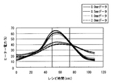
- FIG. 7 is a graph showing the relationship between the processing time and the change in the power supplied to the heater 6a when processing is performed based on the TiN film forming recipe in the film forming apparatus 100.
- 0.0 mm normal surface contact state
- 0.5 mm, 1.0 mm, and 2.0 mm gaps are intentionally provided between the stage 3 and the wafer W to place the wafer W thereon. The experiment was conducted.
- the normal mounting state and the abnormal mounting are obtained by obtaining the ⁇ value or the integrated value of the power supplied to the heater 6a within the processing time of about 50 to 70 seconds from the start. It was confirmed that the state could be easily judged. As described above, it may be possible to make a highly accurate determination by detecting the ⁇ value or the integrated value in a partial section instead of the entire section during processing of one wafer W.
- FIG. 8 shows an integrated value of the power supplied to each heater 6a in the normal placement state, abnormal placement state, and after repair (normal placement state) when a plurality of wafers W are processed in the film forming apparatus 100. Is a graph. As shown in FIG. 8, the integrated value of the power supplied to the heater 6a is greatly different between the normal placement state and the abnormal placement state. Further, since there is a sufficient width (interval between lines on the graph of FIG. 8) between the integrated value in the normal mounting state and the integrated value in the abnormal mounting state, an arbitrary value is set between them. It was also confirmed that it was easy to set the value. Therefore, it is possible to detect the mounting abnormality of the wafer W on the stage 3 by calculating the integrated value of the power supplied to the heater 6a in the normal mounting state and the abnormal mounting state and comparing it with the threshold value. Was confirmed.
- the value of the integrated value A 1 in the processing of the n-th wafer W has been substantially reduced, placed abnormality is detected that has occurred. For this experiment, it can simply detect the placement abnormality of the wafer W even when compared with a predetermined threshold value (e.g., 500 W) the integrated value A 1. Also, in Table 1, it can be seen that the value of the ratio A 1 / A 0 or the difference A 1 -A 0 also varies greatly in the processing of the nth wafer W. Therefore, comparing the ratio A 1 / A 0 with a predetermined threshold (eg 0.9) or comparing the difference A 1 -A 0 with a predetermined threshold (eg -40) Thus, the mounting abnormality of the wafer W could be detected.
- a predetermined threshold e.g 0.9
- comparing the difference A 1 -A 0 with a predetermined threshold eg -40
- the integrated value A 1 of the power supplied to the heater 6a (6b), the ratio A 1 / A 0 or the difference A 1 -A 0 with the integrated value A 0 in the previous wafer W processing is obtained. It was confirmed that the mounting abnormality of the wafer W can be clearly detected by comparing with a predetermined threshold value.
- the present invention is not limited to the above-described embodiments, and various modifications can be made.
- the film forming apparatus 100 has been described as an example of the vacuum apparatus.
- the present invention is not limited to the film forming apparatus, and is not particularly limited as long as the processing apparatus performs a predetermined process while heating the substrate. The present invention can be applied.
- the normal value or the abnormal value is determined by comparing the ⁇ value or the integrated value with the threshold value.
- the abnormal placement state is gradually changed. (For example, a slight abnormal placement state, a severe abnormal placement state, etc.) can also be detected.
- alarm warning and error message caution display and emergency measures such as automatic shutdown of the device can be set and selected according to the detected level of abnormal placement. .
- a single-wafer processing apparatus that provides one stage (substrate mounting table) 3 in the processing container 1 and performs processing for each wafer (substrate) has been described as an example.
- the present invention is not limited to this, and a batch-type processing apparatus is provided that can provide a plurality of stages (substrate mounting tables) 3 in the processing container 1 and perform processing on a plurality of wafers (substrates) at a time.
- the present invention can also be applied.
- a semiconductor wafer has been described as an example of a substrate that is an object to be processed.
- the present invention is not limited to this, and the present invention can be applied to, for example, a glass substrate, an LCD substrate, and a ceramic substrate. Can be applied.
Landscapes
- Chemical & Material Sciences (AREA)
- Engineering & Computer Science (AREA)
- General Chemical & Material Sciences (AREA)
- Chemical Kinetics & Catalysis (AREA)
- Materials Engineering (AREA)
- Mechanical Engineering (AREA)
- Metallurgy (AREA)
- Organic Chemistry (AREA)
- Computer Hardware Design (AREA)
- Manufacturing & Machinery (AREA)
- Microelectronics & Electronic Packaging (AREA)
- Power Engineering (AREA)
- Condensed Matter Physics & Semiconductors (AREA)
- General Physics & Mathematics (AREA)
- Physics & Mathematics (AREA)
- Container, Conveyance, Adherence, Positioning, Of Wafer (AREA)
- Chemical Vapour Deposition (AREA)
- Drying Of Semiconductors (AREA)
Abstract
Description
発明の開示
ヒーターが設けられた基板載置台に載置された基板を加熱しながら処理を行う際に、該基板の載置状態の異常を検知する基板の異常載置状態の検知方法であって、
1枚の基板を処理する間に、前記ヒーターへの電気的出力の情報または前記基板載置台の計測温度の情報に基づいて、前記電気的出力もしくは前記計測温度の最大値および最小値、または、前記電気的出力もしくは前記計測温度の積算値を検出する工程と、
検出された前記最大値および前記最小値、または、検出された前記積算値に基づいて前記基板の異常載置状態を判定する工程と、
を備えている。
ヒーターが設けられた基板載置台に基板を載置する工程と、
前記基板を前記ヒーターで加熱しながら処理する工程と、
処理されている前記基板の載置状態の異常を検知する工程と、を備え、
前記異常を検知する工程が、
1枚の基板を処理する間に、前記ヒーターへの電気的出力の情報または前記基板載置台の計測温度の情報に基づいて、前記電気的出力もしくは前記計測温度の最大値および最小値、または、前記電気的出力もしくは前記計測温度の積算値を検出する工程と、
検出された前記最大値および前記最小値、または、検出された前記積算値に基づいて基板の異常載置状態を判定する工程と、
を有している。
コンピュータ上で動作する制御プログラムが記憶されたコンピュータ読み取り可能な記憶媒体であって、
前記制御プログラムは、ヒーターが設けられた基板載置台に載置された基板を加熱しながら処理を行う際に、
1枚の基板を処理する間に、前記ヒーターへの電気的出力の情報または前記基板載置台の計測温度の情報に基づいて、前記電気的出力もしくは前記計測温度の最大値および最小値、または、前記電気的出力もしくは前記計測温度の積算値を検出する工程と、
検出された前記最大値および前記最小値、または、検出された前記積算値に基づいて基板の異常載置状態を判定する工程と、
を、前記コンピュータに実行させる。
前記基板載置台に設けられ、該基板載置台に載置された基板を加熱するヒーターと、
前記ヒーターに電気的に接続されたヒーター電源と、
前記基板載置台の温度を計測する温度計測部と、
前記ヒーターへの電気的出力または前記基板載置台の計測温度を記憶する記憶部と、
前記ヒーターへの電気的出力の最大値と最小値との差分もしくは該ヒーターへの電気的出力の積算値、または、前記基板載置台の計測温度の最大値と最小値との差分もしくは該基板載置台の計測温度の積算値を検出し、前記差分または前記積算値に基づいて、前記基板の異常載置状態を判定する判定部と、
を備えている。
次に、成膜装置100において行われる本発明の第1の実施の形態にかかるウエハWの異常載置状態の検知方法について説明する。図3は、本実施の形態にかかるウエハWの異常載置状態の検知方法の手順の概略を示すフロー図である。この異常載置状態の検知方法は、成膜装置100で1枚のウエハWを処理する間に行われるものであり、すべてのウエハWの処理を対象に実施してもよいし、ロット中で、選択された任意の数枚のウエハWの処理の際に実施してもよい。
次に、成膜装置100において行われる本発明の第2の実施の形態にかかるウエハWの異常載置状態の検知方法について説明する。図5は、本実施の形態にかかるウエハWの異常載置状態の検知方法の手順の概略を示すフロー図である。なお、以下の説明では、第1の実施の形態との相違点を中心に説明を行い、同様の構成については説明を省略する。

Claims (11)
- ヒーターが設けられた基板載置台に載置された基板を加熱しながら処理を行う際に、該基板の載置状態の異常を検知する基板の異常載置状態の検知方法であって、
1枚の基板を処理する間に、前記ヒーターへの電気的出力の情報または前記基板載置台の計測温度の情報に基づいて、前記電気的出力もしくは前記計測温度の最大値および最小値、または、前記電気的出力もしくは前記計測温度の積算値を検出する工程と、
検出された前記最大値および前記最小値、または、検出された前記積算値に基づいて前記基板の異常載置状態を判定する工程と、
を備えたことを特徴とする基板の異常載置状態の検知方法。 - 前記最大値と前記最小値との差分を求める工程をさらに備え、
前記検出する工程は、前記電気的出力もしくは前記計測温度の最大値および最小値を検出することを含み、
前記判定する工程は、前記差分を所定のしきい値と比較することにより、前記基板の異常載置状態を判定することを含む、ことを特徴とする請求項1に記載の基板の異常載置状態の検知方法。 - 前記最大値と前記最小値との差分を求める工程と、
前記差分と、1枚前の基板の処理において求められた電気的出力または計測温度の最大値および最小値の差分とを用いて演算処理して演算結果を求める工程と、をさらに備え、
前記検出する工程は、前記電気的出力もしくは前記計測温度の最大値および最小値を検出することを含み、
前記判定する工程は、前記演算結果を所定のしきい値と比較することにより、前記基板の異常載置状態を判定することを含む、ことを特徴とする請求項1に記載の基板の異常載置状態の検知方法。 - 前記検出する工程は、前記電気的出力もしくは前記計測温度の積算値を検出することを含み、
前記判定する工程は、前記積算値を所定のしきい値と比較することにより、基板の異常載置状態を判定することを含む、ことを特徴とする請求項1に記載の基板の異常載置状態の検知方法。 - 前記積算値と、1枚前の基板の処理において検出された積算値とを用いて演算処理して演算結果を求める工程をさらに備え、
前記検出する工程は、前記電気的出力もしくは前記計測温度の積算値を検出することを含み、
前記判定する工程は、前記演算結果を所定のしきい値と比較することにより、前記基板の異常載置状態を判定することを含む、ことを特徴とする請求項1に記載の基板の異常載置状態の検知方法。 - 前記積算値をA1とし、1枚前の基板の処理において検出された前記積算値をA0とした場合に、前記演算結果がA1とA0との比からなることを特徴とする請求項5に記載の基板の異常載置状態の検知方法。
- 前記積算値をA1とし、1枚前の基板の処理において検出された前記積算値をA0とした場合に、前記演算結果がA1とA0との差分からなることを特徴とする請求項5に記載の基板の異常載置状態の検知方法。
- 前記検出する工程は、前記電気的出力の最大値および最小値、または、前記電気的出力の積算値を検出することを含み、
前記ヒーターへの電気的出力は、ヒーターへの供給電力、供給電流または供給電圧のいずれか1つ以上であることを特徴とする請求項1に記載の基板の異常載置状態の検知方法。 - ヒーターが設けられた基板載置台に基板を載置する工程と、
前記基板を前記ヒーターで加熱しながら処理する工程と、
処理されている前記基板の載置状態の異常を検知する工程と、を備え、
前記異常を検知する工程は、
1枚の基板を処理する間に、前記ヒーターへの電気的出力の情報または前記基板載置台の計測温度の情報に基づいて、前記電気的出力もしくは前記計測温度の最大値および最小値、または、前記電気的出力もしくは前記計測温度の積算値を検出する工程と、
検出された前記最大値および前記最小値、または、検出された前記積算値に基づいて基板の異常載置状態を判定する工程と、
を有していることを特徴とする基板処理方法。 - コンピュータ上で動作する制御プログラムが記憶されたコンピュータ読み取り可能な記憶媒体であって、
前記制御プログラムは、ヒーターが設けられた基板載置台に載置された基板を加熱しながら処理を行う際に、
1枚の基板を処理する間に、前記ヒーターへの電気的出力の情報または前記基板載置台の計測温度の情報に基づいて、前記電気的出力もしくは前記計測温度の最大値および最小値、または、前記電気的出力もしくは前記計測温度の積算値を検出する工程と、
検出された前記最大値および前記最小値、または、検出された前記積算値に基づいて基板の異常載置状態を判定する工程と、
を、前記コンピュータに実行させることを特徴とするコンピュータ読み取り可能な記憶媒体。 - 基板を載置する基板載置台と、
前記基板載置台に設けられ、該基板載置台に載置された基板を加熱するヒーターと、
前記ヒーターに電気的に接続されたヒーター電源と、
前記基板載置台の温度を計測する温度計測部と、
前記ヒーターへの電気的出力または前記基板載置台の計測温度を記憶する記憶部と、
前記ヒーターへの電気的出力の最大値と最小値との差分もしくは該ヒーターへの電気的出力の積算値、または、前記基板載置台の計測温度の最大値と最小値との差分もしくは該基板載置台の計測温度の積算値を検出し、前記差分または前記積算値に基づいて、前記基板の異常載置状態を判定する判定部と、
を備えた基板処理装置。
Priority Applications (3)
| Application Number | Priority Date | Filing Date | Title |
|---|---|---|---|
| CN2009801123152A CN101990707B (zh) | 2008-09-30 | 2009-09-25 | 基板的异常载置状态的检测方法、基板处理方法、计算机可读取的存储介质以及基板处理装置 |
| KR1020107022704A KR101182502B1 (ko) | 2008-09-30 | 2009-09-25 | 기판의 이상 배치 상태의 검지 방법, 기판 처리 방법, 컴퓨터 판독 가능한 기억 매체 및 기판 처리 장치 |
| US13/000,140 US8581153B2 (en) | 2008-09-30 | 2009-09-25 | Method of detecting abnormal placement of substrate, substrate processing method, computer-readable storage medium, and substrate processing apparatus |
Applications Claiming Priority (2)
| Application Number | Priority Date | Filing Date | Title |
|---|---|---|---|
| JP2008253937 | 2008-09-30 | ||
| JP2008-253937 | 2008-09-30 |
Publications (1)
| Publication Number | Publication Date |
|---|---|
| WO2010038674A1 true WO2010038674A1 (ja) | 2010-04-08 |
Family
ID=42073438
Family Applications (1)
| Application Number | Title | Priority Date | Filing Date |
|---|---|---|---|
| PCT/JP2009/066644 WO2010038674A1 (ja) | 2008-09-30 | 2009-09-25 | 基板の異常載置状態の検知方法、基板処理方法、コンピュータ読み取り可能な記憶媒体および基板処理装置 |
Country Status (5)
| Country | Link |
|---|---|
| US (1) | US8581153B2 (ja) |
| JP (1) | JP5501718B2 (ja) |
| KR (1) | KR101182502B1 (ja) |
| CN (1) | CN101990707B (ja) |
| WO (1) | WO2010038674A1 (ja) |
Cited By (1)
| Publication number | Priority date | Publication date | Assignee | Title |
|---|---|---|---|---|
| JP2016186962A (ja) * | 2015-03-27 | 2016-10-27 | 東京エレクトロン株式会社 | 熱処理装置、熱処理における異常検出方法及び読み取り可能なコンピュータ記憶媒体 |
Families Citing this family (27)
| Publication number | Priority date | Publication date | Assignee | Title |
|---|---|---|---|---|
| JP4871264B2 (ja) * | 2005-03-17 | 2012-02-08 | 浜松ホトニクス株式会社 | 顕微鏡画像撮像装置 |
| JP5299442B2 (ja) * | 2011-01-18 | 2013-09-25 | 東京エレクトロン株式会社 | 基板加熱装置、基板加熱方法及び記憶媒体 |
| JP5616279B2 (ja) * | 2011-04-12 | 2014-10-29 | 東京エレクトロン株式会社 | 基板保持装置、基板処理装置、基板処理方法、及び基板処理プログラムを記録したコンピュータ読み取り可能な記録媒体 |
| NL2007114C2 (en) * | 2011-07-14 | 2013-01-15 | Levitech B V | Floating substrate monitoring and control device, and method for the same. |
| JP5824372B2 (ja) * | 2012-01-25 | 2015-11-25 | 東京エレクトロン株式会社 | 処理装置及びプロセス状態の確認方法 |
| JP5961001B2 (ja) * | 2012-02-14 | 2016-08-02 | 株式会社アルバック | 基板吸着状態の監視方法 |
| US9885567B2 (en) * | 2013-08-27 | 2018-02-06 | Applied Materials, Inc. | Substrate placement detection in semiconductor equipment using thermal response characteristics |
| JP6330297B2 (ja) * | 2013-11-27 | 2018-05-30 | 富士ゼロックス株式会社 | 画像処理装置、画像処理システム、および画像処理プログラム |
| CN104180823B (zh) * | 2014-01-10 | 2016-08-17 | 中国商用飞机有限责任公司北京民用飞机技术研究中心 | 一种温度补偿方法及装置 |
| CN104952752A (zh) * | 2014-03-28 | 2015-09-30 | 中芯国际集成电路制造(上海)有限公司 | 晶圆位置倾斜的侦测方法 |
| TWI662622B (zh) * | 2015-01-14 | 2019-06-11 | 聯華電子股份有限公司 | 避免晶圓加熱過久之方法及其系統 |
| JP6581387B2 (ja) * | 2015-05-12 | 2019-09-25 | 株式会社日立ハイテクノロジーズ | プラズマ処理装置およびプラズマ処理方法 |
| JP6737575B2 (ja) * | 2015-09-30 | 2020-08-12 | Aiメカテック株式会社 | 基板組立システム、そのシステムに用いる基板組立装置、及び、そのシステムを用いた基板組立方法 |
| JP2017073498A (ja) * | 2015-10-08 | 2017-04-13 | 株式会社ニューフレアテクノロジー | 気相成長装置および異常検出方法 |
| KR102592921B1 (ko) | 2015-12-31 | 2023-10-23 | 삼성전자주식회사 | 패턴 결함 검사 방법 |
| JP6617963B2 (ja) * | 2016-02-17 | 2019-12-11 | 株式会社Screenホールディングス | 基板保持状態の異常検査の検査領域の自動決定方法および基板処理装置 |
| JP6695190B2 (ja) * | 2016-03-29 | 2020-05-20 | 東京エレクトロン株式会社 | 異常検知システム及び制御ボード |
| JP6772531B2 (ja) * | 2016-04-28 | 2020-10-21 | オムロン株式会社 | 制御システム、制御方法、制御プログラム、および記録媒体 |
| KR102282631B1 (ko) * | 2016-08-31 | 2021-07-28 | 가부시키가이샤 코쿠사이 엘렉트릭 | 기판 처리 장치, 반도체 장치의 제조 방법 및 프로그램 |
| KR102467605B1 (ko) * | 2017-06-28 | 2022-11-16 | 도쿄엘렉트론가부시키가이샤 | 열처리 장치, 열처리 장치의 관리 방법 및 기억 매체 |
| CN107942965B (zh) * | 2017-11-02 | 2019-08-02 | 芜湖东旭光电科技有限公司 | 玻璃基板成型异常的监控方法及系统 |
| JP6959879B2 (ja) * | 2018-02-08 | 2021-11-05 | 株式会社Screenホールディングス | データ処理方法、データ処理装置、および、データ処理プログラム |
| JP7048351B2 (ja) * | 2018-02-28 | 2022-04-05 | 株式会社Screenホールディングス | 熱処理方法および熱処理装置 |
| JP6874719B2 (ja) * | 2018-03-02 | 2021-05-19 | オムロン株式会社 | 加熱装置及び加熱装置の異常検知方法 |
| JP2020035834A (ja) * | 2018-08-28 | 2020-03-05 | キオクシア株式会社 | 加熱処理装置および加熱処理方法 |
| JP2020177785A (ja) * | 2019-04-17 | 2020-10-29 | 日本電産株式会社 | プラズマ処理装置 |
| JP7467274B2 (ja) * | 2020-08-07 | 2024-04-15 | 東京エレクトロン株式会社 | 温度推定方法及び成膜装置 |
Citations (3)
| Publication number | Priority date | Publication date | Assignee | Title |
|---|---|---|---|---|
| JPH10189692A (ja) * | 1996-12-26 | 1998-07-21 | Shibaura Eng Works Co Ltd | ウェハズレ検出装置 |
| JP2000306825A (ja) * | 1999-02-16 | 2000-11-02 | Tokyo Electron Ltd | 処理装置、処理システム、判別方法及び検出方法 |
| JP2002043231A (ja) * | 2000-07-26 | 2002-02-08 | Shibaura Mechatronics Corp | ウェハの位置ずれ検出方法及び検出装置 |
Family Cites Families (47)
| Publication number | Priority date | Publication date | Assignee | Title |
|---|---|---|---|---|
| US5200023A (en) * | 1991-08-30 | 1993-04-06 | International Business Machines Corp. | Infrared thermographic method and apparatus for etch process monitoring and control |
| US5444217A (en) * | 1993-01-21 | 1995-08-22 | Moore Epitaxial Inc. | Rapid thermal processing apparatus for processing semiconductor wafers |
| US6140612A (en) * | 1995-06-07 | 2000-10-31 | Lam Research Corporation | Controlling the temperature of a wafer by varying the pressure of gas between the underside of the wafer and the chuck |
| US5956489A (en) * | 1995-06-07 | 1999-09-21 | Microsoft Corporation | Transaction replication system and method for supporting replicated transaction-based services |
| TW331652B (en) * | 1995-06-16 | 1998-05-11 | Ebara Corp | Thin film vapor deposition apparatus |
| JP3380668B2 (ja) * | 1996-01-23 | 2003-02-24 | 東京エレクトロン株式会社 | 温度調整方法、温度調整装置及び熱処理装置 |
| US5702624A (en) * | 1996-10-09 | 1997-12-30 | Taiwan Semiconductors Manfuacturing Company, Ltd | Compete hot plate temperature control system for hot treatment |
| KR100551980B1 (ko) * | 1997-11-03 | 2006-02-20 | 에이에스엠 아메리카, 인코포레이티드 | 저질량 지지체를 이용한 웨이퍼의 처리방법 및 장치 |
| US6654668B1 (en) * | 1999-02-16 | 2003-11-25 | Tokyo Electron Limited | Processing apparatus, processing system, distinguishing method, and detecting method |
| US6191394B1 (en) * | 1999-05-19 | 2001-02-20 | Tokyo Electron Ltd. | Heat treating apparatus |
| US6592673B2 (en) * | 1999-05-27 | 2003-07-15 | Applied Materials, Inc. | Apparatus and method for detecting a presence or position of a substrate |
| US6355108B1 (en) * | 1999-06-22 | 2002-03-12 | Applied Komatsu Technology, Inc. | Film deposition using a finger type shadow frame |
| US6100506A (en) * | 1999-07-26 | 2000-08-08 | International Business Machines Corporation | Hot plate with in situ surface temperature adjustment |
| US6313441B1 (en) * | 1999-08-18 | 2001-11-06 | Applied Materials, Inc. | Control system and method for providing variable ramp rate operation of a thermal cycling system |
| US7015422B2 (en) * | 2000-12-21 | 2006-03-21 | Mattson Technology, Inc. | System and process for heating semiconductor wafers by optimizing absorption of electromagnetic energy |
| KR100412262B1 (ko) * | 2001-01-31 | 2003-12-31 | 삼성전자주식회사 | 베이크 장치 |
| KR101067901B1 (ko) * | 2001-12-26 | 2011-09-28 | 맷슨 테크날러지 캐나다 인코퍼레이티드 | 온도 측정 및 열처리 방법과 시스템 |
| US6723201B2 (en) * | 2002-02-21 | 2004-04-20 | Taiwan Semiconductor Manufacturing Co., Ltd. | Microchip fabrication chamber wafer detection |
| JP4030787B2 (ja) * | 2002-03-04 | 2008-01-09 | 東京エレクトロン株式会社 | 基板加熱方法、基板加熱装置及び塗布、現像装置 |
| US20030173346A1 (en) * | 2002-03-18 | 2003-09-18 | Renken Wayne Glenn | System and method for heating and cooling wafer at accelerated rates |
| WO2004019396A1 (ja) * | 2002-08-13 | 2004-03-04 | Tokyo Electron Limited | プラズマ処理方法及びプラズマ処理装置 |
| US20040261930A1 (en) * | 2003-03-04 | 2004-12-30 | Shibaura Mechatronics Corporation | Method of bonding substrates and apparatus for bonding substrates |
| JP4121122B2 (ja) * | 2003-04-01 | 2008-07-23 | 東京エレクトロン株式会社 | 熱処理装置および熱処理装置内温度制御方法 |
| US7138629B2 (en) * | 2003-04-22 | 2006-11-21 | Ebara Corporation | Testing apparatus using charged particles and device manufacturing method using the testing apparatus |
| KR20050026598A (ko) * | 2003-09-09 | 2005-03-15 | 삼성전자주식회사 | 전기조리기 및 그 제어방법 |
| US20050092254A1 (en) * | 2003-10-31 | 2005-05-05 | Infineon Technologies Richmond, Lp | PVD transfer robot short blade |
| US6940047B2 (en) * | 2003-11-14 | 2005-09-06 | Asm International N.V. | Heat treatment apparatus with temperature control system |
| US6980876B2 (en) * | 2004-02-26 | 2005-12-27 | Taiwan Semiconductor Manufacturing Co., Ltd. | Temperature-sensing wafer position detection system and method |
| JP4490704B2 (ja) * | 2004-02-27 | 2010-06-30 | 株式会社日立ハイテクノロジーズ | プラズマ処理方法 |
| US7211196B2 (en) * | 2004-03-26 | 2007-05-01 | Tokyo Electron Limited | Method and system of discriminating substrate type |
| US20050223993A1 (en) * | 2004-04-08 | 2005-10-13 | Blomiley Eric R | Deposition apparatuses; methods for assessing alignments of substrates within deposition apparatuses; and methods for assessing thicknesses of deposited layers within deposition apparatuses |
| TW200612512A (en) * | 2004-06-28 | 2006-04-16 | Ngk Insulators Ltd | Substrate heating sapparatus |
| JP4628071B2 (ja) * | 2004-11-30 | 2011-02-09 | 矢崎総業株式会社 | 車両用熱線ヒータ制御装置 |
| JP4216263B2 (ja) * | 2005-03-09 | 2009-01-28 | シャープ株式会社 | 製造検査解析システム、および製造検査解析方法 |
| JP4786925B2 (ja) | 2005-04-04 | 2011-10-05 | 東京エレクトロン株式会社 | 基板処理方法および基板処理装置 |
| JP2007035899A (ja) * | 2005-07-27 | 2007-02-08 | Sumitomo Electric Ind Ltd | ウエハプローバ用ウエハ保持体及びそれを搭載したウエハプローバ |
| JP2007066923A (ja) * | 2005-08-29 | 2007-03-15 | Matsushita Electric Ind Co Ltd | ウェーハレベルバーンイン方法およびウェーハレベルバーンイン装置 |
| US7956310B2 (en) * | 2005-09-30 | 2011-06-07 | Tokyo Electron Limited | Stage, substrate processing apparatus, plasma processing apparatus, control method for stage, control method for plasma processing apparatus, and storage media |
| JP2007123643A (ja) * | 2005-10-31 | 2007-05-17 | Matsushita Electric Ind Co Ltd | 成膜装置、成膜方法、成膜装置のモニタリングプログラムおよびその記録媒体 |
| KR20070069802A (ko) * | 2005-12-28 | 2007-07-03 | 엘지.필립스 엘시디 주식회사 | 평판표시소자의 제조장치 및 그를 이용한 기판파손방지방법 |
| US7825672B2 (en) * | 2006-06-19 | 2010-11-02 | Mrl Industries, Inc. | High accuracy in-situ resistance measurements methods |
| JP4391518B2 (ja) * | 2006-12-28 | 2009-12-24 | 東京エレクトロン株式会社 | 温度制御方法、調整装置、温度調節器、プログラム、記録媒体および加熱処理装置 |
| CN101246833A (zh) | 2007-02-12 | 2008-08-20 | Psk有限公司 | 基底位置检测方法、基底处理方法和基底处理装置 |
| JP2008234850A (ja) * | 2007-03-16 | 2008-10-02 | Matsushita Electric Ind Co Ltd | 電気化学素子とその電極の製造方法、製造装置 |
| US7739637B2 (en) * | 2007-08-31 | 2010-06-15 | International Business Machines Corporation | Partial good schema for integrated circuits having parallel execution units |
| US20090120584A1 (en) * | 2007-11-08 | 2009-05-14 | Applied Materials, Inc. | Counter-balanced substrate support |
| US8507028B2 (en) * | 2008-12-04 | 2013-08-13 | Linde North America, Inc. | Visualization and enhancement of latent fingerprints using low pressure dye vapor deposition |
-
2009
- 2009-09-25 WO PCT/JP2009/066644 patent/WO2010038674A1/ja active Application Filing
- 2009-09-25 US US13/000,140 patent/US8581153B2/en active Active
- 2009-09-25 KR KR1020107022704A patent/KR101182502B1/ko active IP Right Grant
- 2009-09-25 CN CN2009801123152A patent/CN101990707B/zh active Active
- 2009-09-30 JP JP2009225983A patent/JP5501718B2/ja active Active
Patent Citations (3)
| Publication number | Priority date | Publication date | Assignee | Title |
|---|---|---|---|---|
| JPH10189692A (ja) * | 1996-12-26 | 1998-07-21 | Shibaura Eng Works Co Ltd | ウェハズレ検出装置 |
| JP2000306825A (ja) * | 1999-02-16 | 2000-11-02 | Tokyo Electron Ltd | 処理装置、処理システム、判別方法及び検出方法 |
| JP2002043231A (ja) * | 2000-07-26 | 2002-02-08 | Shibaura Mechatronics Corp | ウェハの位置ずれ検出方法及び検出装置 |
Cited By (1)
| Publication number | Priority date | Publication date | Assignee | Title |
|---|---|---|---|---|
| JP2016186962A (ja) * | 2015-03-27 | 2016-10-27 | 東京エレクトロン株式会社 | 熱処理装置、熱処理における異常検出方法及び読み取り可能なコンピュータ記憶媒体 |
Also Published As
| Publication number | Publication date |
|---|---|
| KR101182502B1 (ko) | 2012-09-12 |
| US8581153B2 (en) | 2013-11-12 |
| JP5501718B2 (ja) | 2014-05-28 |
| CN101990707B (zh) | 2013-03-06 |
| KR20110038607A (ko) | 2011-04-14 |
| JP2010109350A (ja) | 2010-05-13 |
| CN101990707A (zh) | 2011-03-23 |
| US20110174800A1 (en) | 2011-07-21 |
Similar Documents
| Publication | Publication Date | Title |
|---|---|---|
| JP5501718B2 (ja) | 基板の異常載置状態の検知方法、基板処理方法、コンピュータ読み取り可能な記憶媒体および基板処理装置 | |
| KR100887445B1 (ko) | 기판 처리 방법 및 기판 처리 장치 | |
| US8121799B2 (en) | Life estimating method for heater wire, heating apparatus, storage medium, and life estimating system for heater wire | |
| US10607869B2 (en) | Substrate processing system and control device | |
| KR100882633B1 (ko) | 열처리 장치, 열처리 방법, 제어 장치 및 프로그램을 기록한 컴퓨터 판독 가능한 기록 매체 | |
| US10236223B2 (en) | Substrate processing method, program, apparatus and system to determine substrate processing result | |
| JP2006186280A (ja) | 半導体製造装置及び記憶媒体 | |
| TWI729673B (zh) | 基板處理裝置、半導體裝置之製造方法及記錄媒體 | |
| JP6584350B2 (ja) | 制御装置、基板処理システム、基板処理方法及びプログラム | |
| JP6864705B2 (ja) | 基板処理装置、制御システム及び半導体装置の製造方法 | |
| JP4877713B2 (ja) | 基板処理方法 | |
| TWI720520B (zh) | 半導體裝置之製造方法、基板處理裝置及程式 | |
| CN115642104A (zh) | 基板处理装置、半导体器件的制造方法及记录介质 | |
| JP6802903B2 (ja) | 基板処理装置及びその表示方法並びに半導体装置の製造方法 | |
| US9772624B2 (en) | Control apparatus, substrate processing apparatus, and substrate processing system | |
| WO2019053869A1 (ja) | 基板処理装置 | |
| JP2005333032A (ja) | モニタ用被処理体の温度換算関数の形成方法、温度分布の算出方法及び枚葉式の熱処理装置 | |
| EP4379782A1 (en) | Heater life prediction method, heat treatment apparatus, and heater life prediction program | |
| JP2006114638A (ja) | 熱処理装置、熱処理方法及び昇温レートの算出方法 | |
| JP2013239656A (ja) | 基板処理装置 | |
| JP2017168726A (ja) | 制御装置、基板処理システム、基板処理方法及びプログラム | |
| JP2009238997A (ja) | 半導体装置の製造方法および半導体製造装置 |
Legal Events
| Date | Code | Title | Description |
|---|---|---|---|
| WWE | Wipo information: entry into national phase |
Ref document number: 200980112315.2 Country of ref document: CN |
|
| 121 | Ep: the epo has been informed by wipo that ep was designated in this application |
Ref document number: 09817707 Country of ref document: EP Kind code of ref document: A1 |
|
| ENP | Entry into the national phase |
Ref document number: 20107022704 Country of ref document: KR Kind code of ref document: A |
|
| WWE | Wipo information: entry into national phase |
Ref document number: 13000140 Country of ref document: US |
|
| NENP | Non-entry into the national phase |
Ref country code: DE |
|
| 122 | Ep: pct application non-entry in european phase |
Ref document number: 09817707 Country of ref document: EP Kind code of ref document: A1 |