WO2010035876A1 - 発振回路および映像表示装置 - Google Patents
発振回路および映像表示装置 Download PDFInfo
- Publication number
- WO2010035876A1 WO2010035876A1 PCT/JP2009/066979 JP2009066979W WO2010035876A1 WO 2010035876 A1 WO2010035876 A1 WO 2010035876A1 JP 2009066979 W JP2009066979 W JP 2009066979W WO 2010035876 A1 WO2010035876 A1 WO 2010035876A1
- Authority
- WO
- WIPO (PCT)
- Prior art keywords
- signal
- clock
- clock signal
- generator
- oscillation
- Prior art date
- Legal status (The legal status is an assumption and is not a legal conclusion. Google has not performed a legal analysis and makes no representation as to the accuracy of the status listed.)
- Ceased
Links
Images




Classifications
-
- G—PHYSICS
- G09—EDUCATION; CRYPTOGRAPHY; DISPLAY; ADVERTISING; SEALS
- G09G—ARRANGEMENTS OR CIRCUITS FOR CONTROL OF INDICATING DEVICES USING STATIC MEANS TO PRESENT VARIABLE INFORMATION
- G09G5/00—Control arrangements or circuits for visual indicators common to cathode-ray tube indicators and other visual indicators
- G09G5/003—Details of a display terminal, the details relating to the control arrangement of the display terminal and to the interfaces thereto
- G09G5/006—Details of the interface to the display terminal
- G09G5/008—Clock recovery
-
- H—ELECTRICITY
- H03—ELECTRONIC CIRCUITRY
- H03L—AUTOMATIC CONTROL, STARTING, SYNCHRONISATION OR STABILISATION OF GENERATORS OF ELECTRONIC OSCILLATIONS OR PULSES
- H03L7/00—Automatic control of frequency or phase; Synchronisation
- H03L7/06—Automatic control of frequency or phase; Synchronisation using a reference signal applied to a frequency- or phase-locked loop
- H03L7/16—Indirect frequency synthesis, i.e. generating a desired one of a number of predetermined frequencies using a frequency- or phase-locked loop
- H03L7/18—Indirect frequency synthesis, i.e. generating a desired one of a number of predetermined frequencies using a frequency- or phase-locked loop using a frequency divider or counter in the loop
-
- G—PHYSICS
- G09—EDUCATION; CRYPTOGRAPHY; DISPLAY; ADVERTISING; SEALS
- G09G—ARRANGEMENTS OR CIRCUITS FOR CONTROL OF INDICATING DEVICES USING STATIC MEANS TO PRESENT VARIABLE INFORMATION
- G09G3/00—Control arrangements or circuits, of interest only in connection with visual indicators other than cathode-ray tubes
- G09G3/20—Control arrangements or circuits, of interest only in connection with visual indicators other than cathode-ray tubes for presentation of an assembly of a number of characters, e.g. a page, by composing the assembly by combination of individual elements arranged in a matrix no fixed position being assigned to or needed to be assigned to the individual characters or partial characters
- G09G3/34—Control arrangements or circuits, of interest only in connection with visual indicators other than cathode-ray tubes for presentation of an assembly of a number of characters, e.g. a page, by composing the assembly by combination of individual elements arranged in a matrix no fixed position being assigned to or needed to be assigned to the individual characters or partial characters by control of light from an independent source
- G09G3/36—Control arrangements or circuits, of interest only in connection with visual indicators other than cathode-ray tubes for presentation of an assembly of a number of characters, e.g. a page, by composing the assembly by combination of individual elements arranged in a matrix no fixed position being assigned to or needed to be assigned to the individual characters or partial characters by control of light from an independent source using liquid crystals
- G09G3/3611—Control of matrices with row and column drivers
Definitions
- the present invention relates to an oscillation circuit and a video display device.
- FIG. 7 is a configuration diagram of a circuit for displaying an image.
- a TFT (Thin Film Transistor) liquid crystal display device 105 that displays a video signal from an image output circuit unit 102 that generates and outputs various images such as navigation images is supplied from the display timing circuit unit 103.
- the video signal is sampled based on the sampling clock and rendered.
- the display timing circuit unit 103 generates a sampling clock synchronized with the horizontal synchronization signal from the image output circuit unit 102 based on the signal oscillated by the oscillation circuit unit 106.
- FIG. 8 and 9 are timing charts showing the relationship between the clock of the input video signal and the sampling clock.
- the clock of the input video signal matches the sampling clock
- the video signal is correctly sampled in the TFT liquid crystal display device 105, and the video is displayed properly.
- the clock of the input video signal and the sampling clock do not match
- the video signal is not correctly sampled in the TFT liquid crystal display device 105, and the video is displayed improperly.
- the displayed characters are blurred or blurred.
- Patent Document 1 discloses an image display device that changes the frequency division ratio of a frequency divider of a PLL (Phase-Locked Loop) circuit.
- Patent Document 2 discloses a clock generation circuit capable of frequency conversion with a simple configuration by partially masking a sampling clock.
- the number of sampling clocks in one cycle of the horizontal synchronization signal can be calculated as the clock of the video signal.
- blurring and outline blurring of characters occur due to a slight difference between the clock cycle of the video signal and the cycle of the sampling clock.
- the present invention has been made in view of such problems, and provides an oscillation circuit and a video display device that can prevent blurring of characters and blurring of outlines without changing the frequency division ratio of the frequency divider. Is an issue.
- a frequency divider that has a fixed frequency division ratio, divides a predetermined oscillation signal by the frequency division ratio and outputs a frequency division signal, a phase of a synchronization signal included in a video signal, and the frequency
- a phase comparator that compares a phase difference with the phase of the frequency-divided signal output from the frequency divider, and a generator that generates a sampling signal having a period corresponding to a comparison result in the phase comparator.
- An oscillation circuit that supplies the predetermined oscillation signal to the generation circuit, the clock signal generation unit generating a clock signal having a period according to the comparison result in the phase comparator, and the clock signal generation unit
- a clock signal mask unit that masks a part of a clock signal to generate the predetermined oscillation signal and supplies the predetermined oscillation signal to the frequency divider, and the clock signal mask unit includes the generator Produces the sample Period of signal masks the portion of the clock signal to be equal to the predetermined period is the period of the clock used in generating the video signal.
- the oscillation circuit can be connected to the generation circuit and adjusts the period of the sampling signal output from the generation circuit.
- the generation circuit includes a frequency divider, a phase comparator, and a generator, and the generator generates a sampling signal having a period corresponding to the comparison result in the phase comparator.
- the frequency divider in the generation circuit has a fixed frequency division ratio. When any oscillation signal is input, the frequency divider divides the signal by the frequency division ratio and sends it to the phase comparator.
- the oscillation signal input to the frequency divider is referred to as a predetermined oscillation signal.
- the phase comparator of the generation circuit compares the phase of the synchronization signal input from the outside with the phase from the frequency divider.
- the synchronization signal is a signal for synchronizing with the video signal, and examples thereof include a horizontal synchronization signal and a vertical synchronization signal.
- the oscillation circuit makes it possible to adjust the period of the sampling signal generated by the generator of such a generation circuit. Note that this oscillation circuit is connected to the generation circuit and adjusts the period of the sampling signal output from the generation circuit, and thus can be regarded as a circuit that controls the operation of the generation circuit.
- the clock signal generation unit included in the oscillation circuit generates a clock signal having a period corresponding to the comparison result in the phase comparator of the generation circuit.
- the clock signal generation unit includes a clock according to the voltage output from the phase comparator of the generation circuit. It is possible to apply a voltage controlled oscillator that can adjust the period.
- the clock signal mask unit included in the oscillation circuit is for sending the clock signal generated by the clock signal generation unit to the frequency divider of the generation circuit, so that a part of the clock signal can be masked. It is configured. Masking a part of the clock signal is to prevent the frequency divider from recognizing a part of the clock signal in the clock signal in which a large number of clocks generated by the clock signal generation unit are continuous. This means that the clock is eliminated by superimposing a different signal on a part of the clock signal.
- the generator of the generation circuit since the generator of the generation circuit generates a sampling signal having a period corresponding to the comparison result of the phase comparator, the signal sent to the phase comparator is adjusted when it is desired to adjust this signal to a predetermined period.
- the predetermined cycle is a cycle of a clock used when generating a video signal, and is a cycle determined from, for example, a specification of the number of pixels of a circuit that generates a video signal.
- the oscillation circuit masks only a part of the clock signal to the phase comparator so that the period of the sampling signal output from the generator coincides with the predetermined period.
- the phase comparator By masking a part of the clock signal sent to the phase comparator, the phase comparator outputs the output from the generator in order to change the output of the sampling signal output from the generator by mistake. As a result, the period of the sampling clock is shortened. Therefore, the oscillation circuit can adjust the sampling clock generated by the generation circuit to a desired cycle without changing the frequency division ratio of the frequency divider used in the generation circuit. According to the present invention, by adding such a small circuit, it is possible to eliminate the discrepancy between the clock cycle of the video signal and the cycle of the sampling clock while effectively using the existing generation circuit.
- the clock signal masking unit is configured to mask a predetermined number of clocks of the clock signal, and the predetermined number is determined based on the predetermined period and a frequency division ratio of the frequency divider. May be.
- the sampling clock generated by the generator is determined by the frequency division ratio of the frequency divider and the number of clocks masked by the clock signal mask unit. The number of clocks to be masked can be determined from the relationship between the period and the frequency division ratio. Therefore, the sampling clock generated by the generation circuit can be adjusted to a desired cycle.
- the generator outputs a synchronization signal synchronized with the sampling signal to the clock signal mask unit, and the clock signal mask unit is configured to output the clock signal based on the synchronization signal output from the generator. A part may be masked.
- the clock signal mask unit may start masking the clock signal immediately after the synchronization signal output from the generator is input, or may receive the synchronization signal output from the generator. The clock signal masking may be started after a predetermined time has elapsed.
- the clock signal masking unit may start masking the clock signal after a predetermined time has elapsed since the generator started generating the sampling signal.
- the masking process is not started until a predetermined time elapses, so that the operation of the generation circuit can be stabilized quickly.
- the oscillation circuit directly passes the clock signal generated by the clock signal generation unit to the frequency divider by bypassing the clock signal mask unit for a certain time after the generator starts generating the sampling signal. It may further comprise a switch configured to supply, and the synchronization signal output from the generator is cut for a certain period of time after the generator starts generating the sampling signal. You may further have the switch comprised in this way.
- the present invention is also a video display device that receives a video signal and displays a video, wherein the video signal is sampled with a sampling signal to display the video, and the sampling that is supplied to the video display circuit
- a frequency divider that divides by a ratio and outputs a divided signal, and compares the phase difference between the phase of the synchronizing signal included in the video signal and the phase of the divided signal output from the divider
- a generator for generating the sampling signal having a period corresponding to the comparison result in the phase comparator
- the oscillation circuit is a clock having a period corresponding to the comparison result in the phase comparator.
- the clock signal masking unit includes a clock signal masking unit configured to generate the clock signal so that a cycle of the sampling signal generated by the generator is the same as a predetermined cycle applied when generating the video signal. A part may be masked.
- the block diagram of a video display apparatus The block diagram of a clock mask. Timing chart. The timing chart which concerns on a modification. The block diagram of the video display apparatus which concerns on a modification. The block diagram of the video display apparatus which concerns on a modification. The block diagram of the video display apparatus concerning a prior art example. Timing chart when the clocks match. Timing chart when clocks do not match.
- FIG. 1 is a configuration diagram of a video display device 1 to which the present invention is applied.
- the video display device 1 includes an image output circuit unit 2, a display timing circuit unit 3 (an example of a generation circuit), an oscillation circuit unit 4, and a TFT (Thin Film Transistor) liquid crystal display device 5 (video display).
- An example of a circuit The image output circuit unit 2 generates and outputs a video signal such as an operation screen for operating a car navigation screen or various AV (Audio / Visual) devices.
- the image output circuit unit 2 is a circuit unit that generates a video signal by executing a computer program.
- the image output circuit unit 2 independently outputs a composite synchronization signal obtained by combining the horizontal synchronization signal and the vertical synchronization signal and a video signal.
- the following description will be focused on the operation when the horizontal synchronizing signal is used among the composite synchronizing signals.
- the present invention is also applicable to the case where the vertical synchronizing signal is used.
- the video signal output from the image output circuit unit 2 is sent to the TFT liquid crystal display device 5.
- the horizontal synchronization signal output from the image output circuit unit 2 is sent to the display timing circuit unit 3.
- the display timing circuit unit 3 is a generally distributed (commercially available) semiconductor device for video signal processing. As shown in FIG. 1, a phase comparator 31, a timing generator 32 (an example of a generator), and A frequency divider 33 is provided. The display timing circuit unit 3 is based on the premise that the video signal of horizontal 508 pixels is processed. For this reason, the frequency division ratio of the frequency divider 33 is set to 1/508. The frequency divider 33 divides the input oscillation signal by a predetermined frequency division ratio (1/508) and outputs a frequency division signal. That is, every time a 508 clock oscillation signal is input, a 1 clock frequency division signal is output. The phase comparator 31 compares the phases of two input signals, and outputs a voltage signal corresponding to the phase difference.
- the phase comparator 31 receives the horizontal synchronization signal from the image output circuit unit 2 and the frequency-divided signal from the frequency divider 33.
- the output of the phase comparator 31 is sent to a timing generator 32 and a loop filter 41 of the oscillation circuit unit 4 described later. That is, the phase comparator 31 compares the phase of the horizontal synchronizing signal from the image output circuit unit 2 with the phase of the frequency-divided signal from the frequency divider 33, and outputs a voltage signal corresponding to the phase difference to the timing generator 32. And to the loop filter 41.
- the timing generator 32 generates and outputs various signals according to the voltage of the signal output from the phase comparator 31. That is, for example, as shown in FIG.
- the timing generator 32 generates a sampling clock used by the TFT liquid crystal display device 5 to sample the video signal from the image output circuit unit 2 and supplies the sampling clock to the TFT liquid crystal display device 5.
- the horizontal synchronization signal used for adjusting the timing at which the clock mask 43 of the oscillation circuit unit 4 to be described later masks the clock signal is generated and output to the clock mask 43.
- the oscillation circuit unit 4 includes a loop filter 41, a VCO (Voltage Controlled Oscillator) 42 (an example of a clock signal generation unit), and a clock mask 43 (an example of a clock signal mask unit).
- the loop filter 41 is a low-pass filter that removes high-frequency components of the signal output from the phase comparator 31.
- the signal from which the high frequency component has been removed by the loop filter 41 is output to the VCO 42.
- the VCO 42 is a circuit that generates a clock signal having a frequency corresponding to an input voltage.
- the VCO 42 is a voltage-controlled oscillator that can adjust the oscillation frequency of the clock signal according to the input voltage.
- the VCO 42 generates a clock signal having a frequency corresponding to the voltage of the signal output from the loop filter 41 and outputs the clock signal to the clock mask 43.
- the clock mask 43 is a circuit capable of masking the clock signal output from the VCO 42 in accordance with the horizontal synchronization signal output from the timing generator 32.
- FIG. 2 shows the configuration of the clock mask 43. As shown in FIG. 2, the clock mask 43 is provided with a four-stage shift register so that the clock signal from the VCO 42 can be masked for four clocks (an example of a predetermined number). Since the video signal handled in the present embodiment is a color signal, a 12-stage shift register is actually provided so that the clock signal from the VCO 42 can be masked by 12 clocks.
- the clock mask 43 includes a mask for masking the clock signal, a RESET terminal to which a reset signal is input, a DCLK terminal to which a clock signal is input from the VCO 42, an HSYNC terminal to which a horizontal synchronization signal is input from the timing generator 32, and a mask.
- a DCLK_OUT terminal for outputting the clock signal.
- the clock mask 43 includes an XTHRU terminal for outputting an input clock signal without masking, but is not normally used.
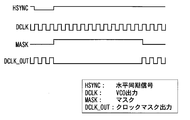
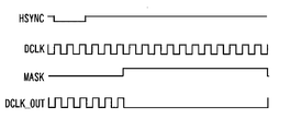
- FIG. 3 shows a timing chart of the operation in which the clock mask 43 masks the clock signal.
- the clock mask 43 when receiving the horizontal synchronization signal from the timing generator 32, the clock mask 43 masks the clock signal from the VCO 42 for four clocks, and clock signals after the fifth clock (predetermined oscillation signal). 1) is output to the frequency divider 33.
- FIG. 3 is a timing chart when masking the clock signal from the VCO 42 for 12 clocks.
- the TFT liquid crystal display device 5 is a liquid crystal display device using a thin film transistor, and samples a video signal from the image output circuit unit 2 based on a sampling clock sent from the display timing circuit unit 3 and other various timing signals. Drawing on the liquid crystal panel. That is, the TFT liquid crystal display device 5 receives the sampling clock output from the timing generator 32 and the video signal output from the image output circuit unit 2. The TFT liquid crystal display device 5 displays an image based on the input sampling clock and the image signal.
- the frequency division ratio of the frequency divider 33 of the display timing circuit unit 3 is increased.
- a sampling clock having a period corresponding to a video signal of horizontal 512 pixels is generated.
- T0 one period of the horizontal synchronization signal corresponding to the video signal of horizontal 508 pixels
- T1 one period of the horizontal synchronization signal corresponding to the video signal of horizontal 512 pixels
- the display timing circuit unit 3 used in the video display device 1 of the present embodiment is a generally-distributed semiconductor device for video signal processing, and is premised on processing a video signal of horizontal 508 pixels. Designed. That is, the frequency division ratio of the frequency divider 33 is fixed to 1/508.
- the phase comparator 31 receives a horizontal synchronization signal (1clk / T0) corresponding to a video signal of 508 pixels in the horizontal direction from the image output circuit unit 2 and a frequency-divided signal (one clock included in the period T0 from the frequency divider 33 ( 1clk / T0) is input, the predetermined voltage V0 is output, and the timing generator 32, based on the predetermined voltage V0, outputs a horizontal synchronization signal (horizontal synchronization signal (508) corresponding to a video signal of 508 pixels in the horizontal direction. 1clk / T0) and a sampling clock (508clk / T0) having a period corresponding to a video signal of 508 pixels in the horizontal direction.
- the VCO 42 of the oscillation circuit unit 4 generates a clock signal (508clk / T0) including 508 clocks in the period T0 and outputs it to the clock mask 43.
- the clock mask 43 masks the clock signal from the VCO 42 by 4 clocks in synchronization with the horizontal synchronization signal (1clk / T0) from the timing generator 32, and the clock signal (504clk / T0) is output. Accordingly, in the period T0, only the oscillation signal of 504 clocks is input to the frequency divider 33, and the oscillation signal of 508 clocks is input to the frequency divider 33 in the period T1 longer than the period T0.
- the frequency divider 33 outputs a frequency-divided signal (1clk / T1) including one clock in the period T1 to the phase comparator 31. That is, the phase comparator 31 receives a horizontal synchronization signal (1 ckl / T1) corresponding to a video signal of horizontal 512 pixels from the image output circuit unit 2, and includes one clock in the cycle T1 from the frequency divider 33. A frequency-divided signal (1clk / T1) is input. In this case, the phase comparator 31 outputs a voltage V1 higher than the predetermined voltage V0 to the loop filter 41 and the timing generator 32.
- the VCO 42 generates a clock signal (512clk / V1) including 512 clocks in the cycle T1 according to the voltage V1 input through the loop filter 41, and outputs the clock signal to the clock mask 43.
- the timing generator 32 generates a sampling clock (512clk / T1) in which 512 clocks are included in the cycle T1, based on the input voltage V1, that is, a sampling clock having a cycle corresponding to a horizontal 512-pixel video signal. It is generated and output to the TFT liquid crystal display device 5.
- the timing generator 32 generates a horizontal synchronization signal having a period corresponding to a horizontal synchronization signal (1clk / T1) in which one clock is included in the period T1, that is, a video signal of horizontal 512 pixels, based on the input voltage V1.
- a signal is generated and output to the clock mask 43.
- the clock mask 43 masks the clock signal (512clk / V1) from the VCO 42 by 4 clocks in synchronization with the horizontal synchronization signal (1clk / T1) from the timing generator 32, and 508 clocks are generated in the cycle T1.
- the included clock signal (508clk / T1) is output. Therefore, an oscillation signal of 508 clocks is input to the frequency divider 33 in the period T1. Therefore, the frequency divider 33 outputs a frequency-divided signal (1clk / T1) including one clock in the period T1 to the phase comparator 31.
- the phase comparator compares the horizontal synchronizing signal (1clk / T1) input from the image output circuit unit 2 with the frequency-divided signal (1clk / T1) input from the frequency divider 33, and compares the voltage V1 with the loop. Output to the filter 41 and the timing generator 32.
- the timing generator 32 generates a sampling clock having a period corresponding to the video signal of horizontal 512 pixels based on the input voltage V1, and outputs the sampling clock to the TFT liquid crystal display device 5.
- the display timing circuit unit 3 designed on the premise of processing a video signal of horizontal 508 pixels is used.
- a sampling clock having a period corresponding to a horizontal 512 pixel video signal can be stably generated.
- the display timing circuit unit 3 and the oscillation circuit unit 4 of the present embodiment constitute a loop circuit.
- the sampling clock frequency is appropriately adjusted in the first loop, and the sampling clock frequency is stabilized in the second loop.
- the sampling clock frequency is gradually converted and stabilized.
- the oscillation circuit unit 4 by adding a small-scale circuit such as the oscillation circuit unit 4 described above, an existing circuit such as the display timing circuit unit 3 described above is effectively used, and the clock cycle of the video signal is increased. And the sampling clock cycle can be eliminated.
- the oscillation circuit unit 4 When the oscillation circuit unit 4 is connected to the display timing circuit unit 3, the signal level and the bypass voltage can be arbitrarily set in order to match the signal level and the bias voltage passed between the two circuits. A circuit or the like may be provided. According to this, the oscillation circuit unit 4 can be widely applied.
- the clock mask 43 when receiving the horizontal synchronization signal from the timing generator 32, the clock mask 43 immediately masks the clock signal from the VCO 42.
- the clock mask 43 may mask the clock signal after a while after receiving the horizontal synchronization signal from the timing generator 32.
- FIG. 4 shows a timing chart in this case. As shown in FIG. 4, it is possible to adjust the timing at which the sampling clock is generated by masking the clock signal after a while after receiving the horizontal synchronization signal. It is possible to adjust the display position of the displayed video, the signal processing delay time in the video processing circuit, and the like.
- the clock mask is immediately performed when the video display device 1 is turned on.
- the clock mask may be started after a predetermined time has elapsed since the power was turned on.
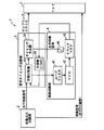
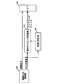
- 5 and 6 are diagrams showing a circuit configuration in this case.
- the clock mask 43 is bypassed and a clock signal is directly sent from the VCO 42 to the frequency divider 33 until a certain time elapses after the video display device 1 is turned on.
- the timer-type switch 44 that moves after a predetermined time is switched, the bypass of the clock mask 43 is released. According to this, since the mask process is not started until a predetermined time elapses, the operation of the display timing circuit unit 3 can be stabilized quickly.
- the horizontal synchronization signal sent from the timing generator 32 to the clock mask 43 is cut from when the video display device 1 is turned on until a predetermined time elapses.
- the timer-type switch 44 that moves after a predetermined time is turned on, the horizontal synchronization signal output from the timing generator 32 is sent to the clock mask 43. Also by this, since the mask process is not started until a certain time elapses, the operation of the display timing circuit unit 3 can be stabilized quickly.
Landscapes
- Engineering & Computer Science (AREA)
- Physics & Mathematics (AREA)
- Computer Hardware Design (AREA)
- General Physics & Mathematics (AREA)
- Theoretical Computer Science (AREA)
- Control Of Indicators Other Than Cathode Ray Tubes (AREA)
- Liquid Crystal Display Device Control (AREA)
- Transforming Electric Information Into Light Information (AREA)
- Stabilization Of Oscillater, Synchronisation, Frequency Synthesizers (AREA)
- Synchronizing For Television (AREA)
Abstract
発振回路が提供される。発振回路は、分周器と、位相比較器と、生成器とを有する生成回路へ所定の発振信号を供給する。クロック信号生成部は、前記位相比較器における比較結果に応じた周期のクロック信号を生成する。クロック信号マスク部は、前記クロック信号生成部が生成した前記クロック信号の一部をマスクして前記所定の発振信号を生成し、該所定の発振信号を前記分周器へ供給する。前記クロック信号マスク部は、前記生成器が生成する前記サンプリング信号の周期が、前記映像信号を生成する際に用いられるクロックの周期である所定周期と同じになるように前記クロック信号の一部をマスクする。
Description
本発明は、発振回路および映像表示装置に関する。
映像信号には、映像表示等を行う機器の仕様に応じて様々な処理が施される。例えば、アナログ映像を表示する場合、入力される映像信号のクロックと同じ周期のサンプリングクロックで映像信号をサンプリング処理する。図7は、映像を表示する回路の構成図である。図7に示すように、ナビゲーション映像等の各種映像を生成して出力する画像出力回路部102からの映像信号を表示するTFT(Thin Film Transistor)液晶表示装置105は、表示タイミング回路部103からのサンプリングクロックに基づいて映像信号をサンプリングし、描画処理する。表示タイミング回路部103は、画像出力回路部102からの水平同期信号と同期したサンプリングクロックを、発振回路部106で発振される信号に基づいて生成する。
図8および図9は、入力される映像信号のクロックとサンプリングクロックとの関係を示すタイミングチャートである。図8に示すように、入力される映像信号のクロックとサンプリングクロックとが一致している場合、TFT液晶表示装置105において映像信号が正しくサンプリングされて、映像が適正に表示される。一方、図9に示すように、入力される映像信号のクロックとサンプリングクロックとが一致していない場合、TFT液晶表示装置105において映像信号が正しくサンプリングされず、映像が不適正に表示される。この場合、表示される文字のにじみや輪郭ぼやけが発生する。
特許文献1には、PLL(Phase-Locked Loop:位相同期ループ)回路の分周器の分周比を変更する画像表示装置が開示されている。また特許文献2には、サンプリングクロックを部分的にマスクすることによって簡単な構成で周波数変換ができるクロック生成回路が開示されている。
映像信号を取り扱う電子機器は、開発コスト等を抑制するため、一般に流通している(市販の)ICチップを流用して映像信号を処理することが多い。つまり、一般に流通しているICチップを、表示タイミング回路部として用いることが多い。このとき、入力される映像信号のクロックと一般に流通しているICチップによって生成されるサンプリングクロックとが一致しないような場合がある。このような場合には、特許文献1の技術を用いて、サンプリングクロックを生成する回路の分周器の分周比を変更することによって、映像信号のクロックとサンプリングクロックを一致させることができるが、分周器の分周比を変更するには多大な費用を要する。また、特許文献2の技術を用いて、分周器の分周比を変更せずにサンプリングクロックを部分的にマスクすることによって、水平同期信号の1周期におけるサンプリングクロックの数を映像信号のクロックの数に合わせることができるが、この場合は、映像信号のクロックの周期とサンプリングクロックの周期との微妙な齟齬によって、文字のにじみや輪郭ぼけが発生してしまう。
本発明は、このような問題に鑑みなされたものであり、分周器の分周比を変更することなく、文字のにじみや輪郭ぼやけを防ぐことができる発振回路および映像表示装置を提供することを課題とする。
本発明は、上記課題を解決するため、分周器へ供するクロック信号の一部をマスクする。
詳細には、固定された分周比を有し、所定の発振信号を該分周比で分周して分周信号を出力する分周器と、映像信号に含まれる同期信号の位相と該分周器から出力される前記分周信号の位相との間の位相差を比較する位相比較器と、該位相比較器における比較結果に応じた周期のサンプリング信号を生成する生成器と、を有する生成回路へ、該所定の発振信号を供給する発振回路であって、前記位相比較器における比較結果に応じた周期のクロック信号を生成するクロック信号生成部と、前記クロック信号生成部が生成した前記クロック信号の一部をマスクして前記所定の発振信号を生成し、該所定の発振信号を前記分周器へ供給するクロック信号マスク部と、を備え、前記クロック信号マスク部は、前記生成器が生成する前記サンプリング信号の周期が、前記映像信号を生成する際に用いられるクロックの周期である所定周期と同じになるように前記クロック信号の一部をマスクする。
上記発振回路は、生成回路に接続可能であって、該生成回路から出力されるサンプリング信号の周期を調整する。この生成回路は、上述のように、分周器と位相比較器と生成器とを有し、生成器は位相比較器における比較結果に応じた周期のサンプリング信号を生成する。生成回路における分周器は、固定された分周比を有し、何らかの発振信号が入力されるとこれを該分周比で分周し、位相比較器へ送る。分周器へ入力される発振信号を、本発明では、所定の発振信号と呼ぶ。生成回路の位相比較器では、外部から入力される同期信号の位相と分周器からの位相とを比較する。同期信号は、映像信号と同期を取るための信号であり、例えば、水平同期信号や垂直同期信号を例示できる。上記発振回路は、このような生成回路の生成器で生成されるサンプリング信号の周期を調整可能にするものである。なお、この発振回路は、生成回路に接続されて、該生成回路から出力されるサンプリング信号の周期を調整するものであるから、生成回路の動作を制御する回路として捉えることもできる。
上記発振回路が備えるクロック信号生成部は、生成回路の位相比較器における比較結果に応じた周期のクロック信号を生成するものであり、例えば、生成回路の位相比較器が出力する電圧に応じてクロックの周期を調整することが可能な電圧制御発振器を適用することができる。
ここで、発振回路が備えるクロック信号マスク部は、クロック信号生成部が生成したクロック信号を生成回路の分周器へ送るものであるが、クロック信号の一部をマスクすることが可能なように構成されている。クロック信号の一部をマスクするとは、クロック信号生成部が生成した多数のクロックが連続しているクロック信号の中の一部のクロックを、分周器が認識できないようにすることであり、例えば、クロック信号の一部に異なる信号を重畳してクロックを無くすことをいう。
ところで、生成回路の生成器では、位相比較器の比較結果に応じた周期のサンプリング信号が生成されるため、この信号を所定周期に調整したい場合には位相比較器へ送られる信号を調整することが肝要である。ここで、所定周期とは、映像信号を生成する際に使われたクロックの周期であり、例えば、映像信号を生成する回路の画素数の仕様等から定まる周期である。上記発振回路は、生成器から出力されるサンプリング信号の周期が、この所定周期と一致するように、位相比較器へのクロック信号を一部だけマスクする。位相比較器へ送られるクロック信号の一部をマスクすることにより、位相比較器は生成器から出力されているサンプリング信号の周期が遅れていると錯誤してその出力を変えるため、生成器から出力されるサンプリングクロックの周期が結果的に早くなる。従って、上記発振回路は、生成回路に用いられている分周器の分周比を変更することなく、生成回路で生成されるサンプリングクロックを所望の周期に調整することができる。本発明によれば、このような小規模の回路追加により、既存の生成回路を有効に活用しながら映像信号のクロックの周期とサンプリングクロックの周期との齟齬を解消することが可能になる。
また、前記クロック信号マスク部は、前記クロック信号の所定個数のクロックをマスクするように構成されており、該所定個数は、前記所定周期と前記分周器の分周比とに基づいて決定されてもよい。生成器で生成されるサンプリングクロックは、分周器の分周比とクロック信号マスク部がマスクするクロックの個数とにより定まるものであるため、サンプリングクロックの周期を所定周期にしたい場合には、所定周期と分周比との関係から、マスクすべきクロック数を決定することができる。よって、生成回路で生成されるサンプリングクロックを所望の周期に調整することが可能である。
また、前記生成器は、前記サンプリング信号と同期する同期信号を前記クロック信号マスク部に出力し、前記クロック信号マスク部は、前記生成器から出力される前記同期信号に基づいて、前記クロック信号の一部をマスクするものであってもよい。このように構成される発振回路であれば、同期信号と同期するサンプリングクロックを安定的に生成させることが可能である。前記クロック信号マスク部は、前記生成器から出力される前記同期信号が入力された直後に、前記クロック信号のマスクを開始してもよいし、前記生成器から出力される前記同期信号を受けてから一定時間が経過した後に、前記クロック信号のマスクを開始してもよい。
また、前記クロック信号マスク部は、前記生成器が前記サンプリング信号の生成を開始してから一定時間が経過した後に、前記クロック信号のマスクを開始するものであってもよい。このように構成される発振回路であれば、一定時間が経過するまでマスク処理が開始されないため、生成回路の動作を一早く安定させることが可能である。前記発振回路は、前記生成器が前記サンプリング信号の生成を開始してから一定時間の間、前記クロック信号生成部が生成したクロック信号を前記クロック信号マスク部をバイパスして前記分周器へ直接供給するように構成されているスイッチを更に有してもよいし、前記生成器が前記サンプリング信号の生成を開始してから一定時間の間、前記生成器から出力される前記同期信号をカットするように構成されているスイッチを更に有してもよい。
また、本発明は、映像信号を受け付けて映像を表示する映像表示装置であって、前記映像信号をサンプリング信号でサンプリングして映像を表示する映像表示回路と、前記映像表示回路へ供給する前記サンプリング信号を生成する生成回路と、前記生成回路へ所定の発振信号を供給する発振回路と、を備え、前記生成回路は、固定された分周比を有し、前記所定の発振信号を該分周比で分周して分周信号を出力する分周器と、前記映像信号に含まれる同期信号の位相と該分周器から出力される前記分周信号の位相との間の位相差を比較する位相比較器と、該位相比較器における比較結果に応じた周期の前記サンプリング信号を生成する生成器と、を有し、前記発振回路は、前記位相比較器における比較結果に応じた周期のクロック信号を生成するクロック信号生成部と、前記クロック信号生成部が生成した前記クロック信号の一部をマスクして前記所定の発振信号を生成し、該所定の発振信号を前記分周器へ供給するクロック信号マスク部と、を有し、前記クロック信号マスク部は、前記生成器が生成する前記サンプリング信号の周期が、前記映像信号を生成する際に適用される所定周期と同じになるように前記クロック信号の一部をマスクするものであってもよい。
分周器の分周比を変更することなく、文字のにじみや輪郭ぼやけを防ぐことができる発振回路および映像表示装置を提供することが可能になる。
以下、この発明を実施するための最良の形態を例示的に説明する。以下に示す実施形態は例示であり、本発明はこれらに限定されない。
図1は、本発明を適用した映像表示装置1の構成図である。映像表示装置1は、図1に示すように、画像出力回路部2、表示タイミング回路部3(生成回路の一例)、発振回路部4、及びTFT(Thin Film Transistor)液晶表示装置5(映像表示回路の一例)で構成される。画像出力回路部2は、カーナビゲーション画面や各種AV(Audio/Visual)機器を操作する操作画面等の映像信号を生成して、出力する。画像出力回路部2は、コンピュータプログラムを実行することで映像信号を生成する回路部である。画像出力回路部2は、各種信号の減衰を抑制するため、水平同期信号と垂直同期信号とを合わせた複合同期信号と、映像信号とをそれぞれ独立に出力する。なお、本実施形態においては、以下、複合同期信号のうち特に水平同期信号を用いた場合の動作を中心に説明するが、本発明は、垂直同期信号を用いた場合についても適用可能である。画像出力回路部2から出力される映像信号は、TFT液晶表示装置5へ送られる。また、画像出力回路部2から出力される水平同期信号は、表示タイミング回路部3へ送られる。
なお、画像出力回路部2から出力される映像信号は水平512画素の信号であり、水平同期信号の周期や映像信号を生成する際のクロックの周期(所定周期の一例)もこれに準じている。画像出力回路部2から出力される映像信号は、赤、緑、青の3つの原色信号で一画素を構成する映像信号であるため、この映像信号の一水平線を走査するには実際には、512×3=1536クロックのサンプリング信号が必要になる。但し、説明の便宜上、以下の説明においては、3つの原色信号で構成される一画素をサンプリングする際に要するクロックを1クロックとして説明する。つまり、水平512画素の映像信号の一水平線を走査するために、512クロックのサンプリング信号が必要になることとして説明する。
表示タイミング回路部3は、一般に流通している(市販の)映像信号処理用の半導体装置であり、図1に示すように、位相比較器31、タイミング生成器32(生成器の一例)、及び分周器33を備える。表示タイミング回路部3は、水平508画素の映像信号を処理することを前提とする仕様になっており、このため分周器33の分周比は、1/508に設定されている。分周器33は、入力される発振信号を既定の分周比(1/508)で分周し、分周信号を出力する。すなわち、508クロックの発振信号が入力される毎に1クロックの分周信号を出力する。位相比較器31は、入力される2つの信号の位相を比較し、位相差に応じた電圧の信号を出力する。この位相比較器31には、画像出力回路部2からの水平同期信号と、分周器33からの分周信号とが入力されている。また、位相比較器31の出力は、タイミング生成器32および後述する発振回路部4のループフィルタ41へ送られる。つまり、位相比較器31は、画像出力回路部2からの水平同期信号の位相と分周器33からの分周信号の位相とを比較し、位相差に応じた電圧の信号をタイミング生成器32およびループフィルタ41へ送る。タイミング生成器32は、位相比較器31から出力される信号の電圧に応じて各種の信号を生成して出力する。すなわち、タイミング生成器32は、例えば図1に示すように、TFT液晶表示装置5が画像出力回路部2からの映像信号をサンプリングするために用いるサンプリングクロックを生成して、TFT液晶表示装置5へ出力し、後述する発振回路部4のクロックマスク43がクロック信号をマスクするタイミングを調整するために用いる水平同期信号を生成して、クロックマスク43へ出力する。
発振回路部4は、図1に示すように、ループフィルタ41、VCO(Voltage Controlled Oscillator)42(クロック信号生成部の一例)、及びクロックマスク43(クロック信号マスク部の一例)で構成される。ループフィルタ41は、位相比較器31から出力される信号の高周波成分を除去するローパスフィルタである。ループフィルタ41によって高周波成分を除去された信号はVCO42へ出力される。VCO42は、入力される電圧に応じた周波数のクロック信号を生成する回路であり、換言すると、入力される電圧によってクロック信号の発振周波数を調整可能な電圧制御発振器である。VCO42は、ループフィルタ41から出力される信号の電圧に応じた周波数のクロック信号を生成し、クロックマスク43へ出力する。クロックマスク43は、VCO42から出力されるクロック信号を、タイミング生成器32から出力される水平同期信号に応じてマスクすることが可能な回路である。図2にクロックマスク43の構成を示す。クロックマスク43は、図2に示すように、VCO42からのクロック信号を4クロック分(所定個数の一例)マスク可能なように4段のシフトレジスタが設けられている。なお、本実施形態で取り扱う映像信号はカラー信号であるため、実際には、VCO42からのクロック信号を12クロック分マスク可能なように12段のシフトレジスタが設けられている。図2には、12段のシフトレジスタが設けられているクロックマスク43が示されている。また、クロックマスク43は、クロック信号をマスクするMASK、リセット信号が入力されるRESET端子、VCO42からクロック信号が入力されるDCLK端子、タイミング生成器32から水平同期信号が入力されるHSYNC端子、マスクされたクロック信号を出力するDCLK_OUT端子を有する。加えて、クロックマスク43は、入力されるクロック信号をマスクしないで出力するためのXTHRU端子を備えているが、通常は使用しない。RESET端子にリセット信号が入力された後、VCO42からDCLK端子に4クロックが入力されると、全ての段のシフトレジスタについてAND条件が成立し、5クロック目以降のVCO42からのクロック信号がクロックマスク43を通過して、DCLK_OUT端子から出力される。図3は、クロックマスク43がクロック信号をマスクする動作のタイミングチャートを示したものである。クロックマスク43は、図3に示すように、タイミング生成器32からの水平同期信号を受けると、VCO42からのクロック信号を4クロック分だけマスクし、5クロック目以降のクロック信号(所定の発振信号の一例)を分周器33へ出力する。なお本実施形態で取り扱う映像信号はカラー信号であるため、実際には、VCO42からのクロック信号を12クロック分だけマスクし、13クロック目以降のクロック信号を分周器へ出力する。図3は、VCO42からのクロック信号を12クロック分だけマスクするときのタイミングチャートである。
TFT液晶表示装置5は、薄膜トランジスタを使った液晶ディスプレイ装置であり、表示タイミング回路部3から送られるサンプリングクロックやその他の各種のタイミング信号に基づいて画像出力回路部2からの映像信号をサンプリングし、液晶パネルに描画処理する。すなわち、TFT液晶表示装置5には、タイミング生成器32から出力されるサンプリングクロックと、画像出力回路部2から出力される映像信号とが入力される。そして、TFT液晶表示装置5は、入力されたサンプリングクロックと映像信号とに基づいて映像を表示する。
このように構成される映像表示装置1では、電源が供給されて画像出力回路部2から映像信号や水平同期信号が出力されると、表示タイミング回路部3の分周器33の分周比が1/508であるにも関わらず、水平512画素の映像信号に対応する周期を有するサンプリングクロックが生成される。以下、本実施形態の映像表示装置1の動作について説明する。以下の説明では、水平508画素の映像信号に対応する水平同期信号の1周期をT0、水平512画素の映像信号に対応する水平同期信号の1周期をT1とする。
本実施形態の映像表示装置1に用いられる表示タイミング回路部3は、前述した通り、一般に流通している映像信号処理用の半導体装置であり、水平508画素の映像信号を処理することを前提として設計されている。つまり、分周器33の分周比は、1/508に固定されている。位相比較器31は、画像出力回路部2から水平508画素の映像信号に対応する水平同期信号(1clk/T0)が入力され、分周器33から周期T0に1クロックが含まれる分周信号(1clk/T0)が入力されると、所定電圧V0を出力するように設計されており、タイミング生成器32は、この所定電圧V0に基づいて、水平508画素の映像信号に対応する水平同期信号(1clk/T0)、および水平508画素の映像信号に対応する周期を有するサンプリングクロック(508clk/T0)を生成するように設計されている。
最初に、発振回路部4のVCO42が周期T0に508クロックが含まれるクロック信号(508clk/T0)を生成して、クロックマスク43に出力していることとする。クロックマスク43は、タイミング生成器32からの水平同期信号(1clk/T0)に同期して、VCO42からのクロック信号を4クロック分だけマスクし、周期T0に504クロックが含まれるクロック信号(504clk/T0)を出力する。従って、周期T0において、分周器33には、504クロックの発振信号しか入力されず、周期T0より長い周期T1において、分周器33に508クロックの発振信号が入力される。このため、分周器33は周期T1に1クロックが含まれる分周信号(1clk/T1)を、位相比較器31に出力する。つまり、位相比較器31には、画像出力回路部2から水平512画素の映像信号に対応する水平同期信号(1ckl/T1)が入力され、また分周器33から周期T1に1クロックが含まれる分周信号(1clk/T1)が入力される。この場合、位相比較器31は、所定電圧V0よりも高い電圧V1を、ループフィルタ41、タイミング生成器32に出力する。すると、VCO42は、ループフィルタ41を介して入力された電圧V1に応じて、周期T1に512クロックが含まれるクロック信号(512clk/V1)を生成して、クロックマスク43に出力するようになる。一方、タイミング生成器32は、入力された電圧V1に基づいて、周期T1に512クロックが含まれるサンプリングクロック(512clk/T1)、すなわち、水平512画素の映像信号に対応する周期を有するサンプリングクロックを生成して、TFT液晶表示装置5へ出力する。また、タイミング生成器32は、入力された電圧V1に基づいて、周期T1に1クロックが含まれる水平同期信号(1clk/T1)、すなわち、水平512画素の映像信号に対応する周期を有する水平同期信号を生成して、クロックマスク43へ出力する。
次いで、クロックマスク43は、タイミング生成器32からの水平同期信号(1clk/T1)に同期して、VCO42からのクロック信号(512clk/V1)を4クロック分だけマスクし、周期T1に508クロックが含まれるクロック信号(508clk/T1)を出力する。従って、周期T1において、分周器33には、508クロックの発振信号が入力される。このため分周器33は、周期T1に1クロックが含まれる分周信号(1clk/T1)を、位相比較器31に出力する。位相比較器は、画像出力回路部2から入力される水平同期信号(1clk/T1)と分周器33から入力される分周信号(1clk/T1)とを比較して、電圧V1を、ループフィルタ41、タイミング生成器32に出力する。タイミング生成器32は、入力された電圧V1に基づいて、水平512画素の映像信号に対応する周期を有するサンプリングクロックを生成して、TFT液晶表示装置5へ出力する。
このようにして、映像表示装置1に発振回路部4を組み込むことによって、水平508画素の映像信号を処理することを前提として設計されている表示タイミング回路部3を用いているにも関わらず、水平512画素の映像信号に対応する周期を有するサンプリングクロックを安定的に生成することができる。
なお、本実施形態の表示タイミング回路部3と発振回路部4とは、ループ回路を構成している。上記の説明では、1回目のループで、サンプリングクロックの周波数を適切に合わせて、2回目のループで、サンプリングクロックの周波数を安定させているが、実際には、複数回のループを繰り返すことによって、徐々にサンプリングクロックの周波数を変換し、安定させている。
本実施形態によれば、上述した発振回路部4のような小規模の回路の追加により、上述した表示タイミング回路部3のような既存の回路を有効に活用しつつ、映像信号のクロックの周期とサンプリングクロックの周期との齟齬を解消することが可能になる。なお、上記発振回路部4を表示タイミング回路部3と接続する場合には、両回路間で受け渡される信号のレベルやバイアス電圧を合わせるために、信号のレベルやバイパス電圧を任意に設定できるインターフェース回路等を設けてもよい。これによれば、発振回路部4を幅広く適用することができる。
また、上記実施形態において、クロックマスク43は、タイミング生成器32からの水平同期信号を受けると、VCO42からのクロック信号を直ちにマスクしていた。しかし、クロックマスク43は、タイミング生成器32からの水平同期信号を受けてからしばらく経った後にクロック信号をマスクしてもよい。図4は、この場合のタイミングチャートを示した図である。図4に示すように、水平同期信号を受けてからしばらく経った後にクロック信号をマスクすることで、サンプリングクロックが生成されるタイミングを調整することが可能であり、例えば、TFT液晶表示装置5に表示される映像の表示位置や映像処理回路における信号処理の遅れ時間等を調整することが可能である。
また、上記実施形態は、映像表示装置1の電源が入るとクロックマスクが直ちに行われていたが、電源が入ってから一定時間が経過後にクロックマスクを開始するようにしてもよい。図5および図6は、この場合の回路構成を示す図である。例えば、図5に示すように、映像表示装置1の電源が入ってから一定時間が経過するまでの間、クロックマスク43をバイパスし、VCO42から分周器33へクロック信号を直接送る。そして、一定時間が経過したら動くタイマー式のスイッチ44が切り替わったら、クロックマスク43のバイパスが解除されるようにする。これによれば、一定時間が経過するまでマスク処理が開始されないため、表示タイミング回路部3の動作を一早く安定させることが可能である。また、図6に示すように、映像表示装置1の電源が入ってから一定時間が経過するまでの間、タイミング生成器32からクロックマスク43へ送られる水平同期信号をカットする。そして、一定時間が経過したら動くタイマー式のスイッチ44がオンになったら、タイミング生成器32から出力される水平同期信号がクロックマスク43へ送られるようにする。これによっても、一定時間が経過するまでマスク処理が開始されないため、表示タイミング回路部3の動作を一早く安定させることが可能である。
本出願は、2008年9月29日出願の日本特許出願・出願番号2008-250465に基づくものであり、その内容はここに参照として取り込まれる。
1 映像表示装置
2,102 画像出力回路部
3,103 表示タイミング回路部
4 発振回路部
5,105 TFT液晶表示装置
31 位相比較器
32 タイミング生成器
33 分周器
41 ループフィルタ
42 VCO
43 クロックマスク
44 スイッチ
106 発振回路部
2,102 画像出力回路部
3,103 表示タイミング回路部
4 発振回路部
5,105 TFT液晶表示装置
31 位相比較器
32 タイミング生成器
33 分周器
41 ループフィルタ
42 VCO
43 クロックマスク
44 スイッチ
106 発振回路部
Claims (9)
- 固定された分周比を有し、所定の発振信号を該分周比で分周して分周信号を出力する分周器と、映像信号に含まれる同期信号の位相と該分周器から出力される前記分周信号の位相との間の位相差を比較する位相比較器と、該位相比較器における比較結果に応じた周期のサンプリング信号を生成する生成器と、を有する生成回路へ、該所定の発振信号を供給する発振回路であって、
前記位相比較器における比較結果に応じた周期のクロック信号を生成するクロック信号生成部と、
前記クロック信号生成部が生成した前記クロック信号の一部をマスクして前記所定の発振信号を生成し、該所定の発振信号を前記分周器へ供給するクロック信号マスク部と、を備え、
前記クロック信号マスク部は、前記生成器が生成する前記サンプリング信号の周期が、前記映像信号を生成する際に用いられるクロックの周期である所定周期と同じになるように前記クロック信号の一部をマスクする。 - 請求項1に記載の発振回路であって、
前記クロック信号マスク部は、前記クロック信号の所定個数のクロックをマスクし、当該所定個数は、前記所定周期と前記分周器の分周比とに基づいて決定される。 - 請求項1または2に記載の発振回路であって、
前記生成器は、前記サンプリング信号と同期する同期信号を前記クロック信号マスク部に出力し、
前記クロック信号マスク部は、前記生成器から出力される前記同期信号に基づいて、前記クロック信号の一部をマスクする。 - 請求項3に記載の発振回路であって、
前記クロック信号マスク部は、前記生成器から出力される前記同期信号が入力された直後に、前記クロック信号のマスクを開始する。 - 請求項3に記載の発振回路であって、
前記クロック信号マスク部は、前記生成器から出力される前記同期信号を受けてから一定時間が経過した後に、前記クロック信号のマスクを開始する。 - 請求項1から5の何れか一項に記載の発振回路であって、
前記クロック信号マスク部は、前記生成器が前記サンプリング信号の生成を開始してから一定時間が経過した後に、前記クロック信号のマスクを開始する。 - 請求項6に記載の発振回路であって、
前記生成器が前記サンプリング信号の生成を開始してから一定時間の間、前記クロック信号生成部が生成したクロック信号を前記クロック信号マスク部をバイパスして前記分周器へ直接供給するように構成されているスイッチを更に有する。 - 請求項6に記載の発振回路であって、
前記生成器が前記サンプリング信号の生成を開始してから一定時間の間、前記生成器から出力される前記同期信号をカットするように構成されているスイッチを更に有する。 - 映像信号を受け付けて映像を表示する映像表示装置であって、
前記映像信号をサンプリング信号でサンプリングして映像を表示する映像表示回路と、
前記映像表示回路へ供給する前記サンプリング信号を生成する生成回路と、
前記生成回路へ所定の発振信号を供給する発振回路と、を備え、
前記生成回路は、固定された分周比を有し、前記所定の発振信号を該分周比で分周して分周信号を出力する分周器と、前記映像信号に含まれる同期信号の位相と該分周器から出力される前記分周信号の位相との間の位相差を比較する位相比較器と、該位相比較器における比較結果に応じた周期の前記サンプリング信号を生成する生成器と、を有し、
前記発振回路は、前記位相比較器における比較結果に応じた周期のクロック信号を生成するクロック信号生成部と、前記クロック信号生成部が生成した前記クロック信号の一部をマスクして前記所定の発振信号を生成し、該所定の発振信号を前記分周器へ供給するクロック信号マスク部と、を有し、
前記クロック信号マスク部は、前記生成器が生成する前記サンプリング信号の周期が、前記映像信号を生成する際に用いられるクロックの周期である所定周期と同じになるように前記クロック信号の一部をマスクする。
Priority Applications (1)
| Application Number | Priority Date | Filing Date | Title |
|---|---|---|---|
| US13/121,050 US8542067B2 (en) | 2008-09-29 | 2009-09-29 | Oscillation circuit and image display device |
Applications Claiming Priority (2)
| Application Number | Priority Date | Filing Date | Title |
|---|---|---|---|
| JP2008250465A JP5242320B2 (ja) | 2008-09-29 | 2008-09-29 | 発振回路、及び映像表示装置 |
| JP2008-250465 | 2008-09-29 |
Publications (1)
| Publication Number | Publication Date |
|---|---|
| WO2010035876A1 true WO2010035876A1 (ja) | 2010-04-01 |
Family
ID=42059863
Family Applications (1)
| Application Number | Title | Priority Date | Filing Date |
|---|---|---|---|
| PCT/JP2009/066979 Ceased WO2010035876A1 (ja) | 2008-09-29 | 2009-09-29 | 発振回路および映像表示装置 |
Country Status (4)
| Country | Link |
|---|---|
| US (1) | US8542067B2 (ja) |
| JP (1) | JP5242320B2 (ja) |
| CN (1) | CN101714860B (ja) |
| WO (1) | WO2010035876A1 (ja) |
Cited By (1)
| Publication number | Priority date | Publication date | Assignee | Title |
|---|---|---|---|---|
| WO2022163576A1 (ja) * | 2021-01-29 | 2022-08-04 | 日本電気株式会社 | 受信装置、量子鍵配送システム及び量子信号の検出方法 |
Families Citing this family (8)
| Publication number | Priority date | Publication date | Assignee | Title |
|---|---|---|---|---|
| JP5414479B2 (ja) * | 2009-11-27 | 2014-02-12 | ルネサスエレクトロニクス株式会社 | 半導体装置 |
| US8400199B2 (en) * | 2010-11-26 | 2013-03-19 | Mediatek Inc. | Charge pump, phase frequency detector and charge pump methods |
| WO2013150698A1 (ja) * | 2012-04-03 | 2013-10-10 | パナソニック株式会社 | 映像信号送信装置及び受信装置 |
| CN103427836A (zh) * | 2013-07-25 | 2013-12-04 | 京东方科技集团股份有限公司 | 一种频率信号发生系统和显示装置 |
| JP6264852B2 (ja) * | 2013-11-14 | 2018-01-24 | 株式会社ソシオネクスト | タイミング調整回路および半導体集積回路装置 |
| US9966965B2 (en) * | 2016-06-10 | 2018-05-08 | Silicon Laboratories Inc. | Apparatus for low power signal generator and associated methods |
| US9712176B1 (en) * | 2016-06-10 | 2017-07-18 | Silicon Laboratories Inc. | Apparatus for low power signal generator and associated methods |
| US10992843B2 (en) * | 2017-08-28 | 2021-04-27 | Novatek Microelectronics Corp. | Video interface conversion apparatus and operation method thereof |
Citations (3)
| Publication number | Priority date | Publication date | Assignee | Title |
|---|---|---|---|---|
| JPH05160721A (ja) * | 1991-12-05 | 1993-06-25 | Toshiba Corp | 分周回路 |
| JP2001308697A (ja) * | 2000-04-24 | 2001-11-02 | Nippon Telegr & Teleph Corp <Ntt> | 周波数生成回路および信号受信回路 |
| JP2007248103A (ja) * | 2006-03-14 | 2007-09-27 | Sharp Corp | 半導体集積回路 |
Family Cites Families (9)
| Publication number | Priority date | Publication date | Assignee | Title |
|---|---|---|---|---|
| JPH04282917A (ja) * | 1991-03-12 | 1992-10-08 | Matsushita Electric Ind Co Ltd | クロック発生装置 |
| JPH06282349A (ja) | 1993-03-29 | 1994-10-07 | Sanyo Electric Co Ltd | サンプリングクロック発生回路 |
| JPH10173518A (ja) | 1996-12-13 | 1998-06-26 | Sony Corp | Pll回路およびそれを用いた画像表示装置 |
| JPH1155555A (ja) | 1997-07-31 | 1999-02-26 | Sony Corp | 基準信号発生装置およびこれを用いたビデオカメラ |
| JP2000286701A (ja) * | 1999-03-31 | 2000-10-13 | Fujitsu General Ltd | 位相同期ループ回路 |
| JP3731510B2 (ja) | 2001-08-24 | 2006-01-05 | 松下電器産業株式会社 | デジタルサンプリングクロック発生装置 |
| JP2003098992A (ja) * | 2001-09-19 | 2003-04-04 | Nec Corp | ディスプレイの駆動方法、その回路及び携帯用電子機器 |
| KR100438786B1 (ko) * | 2002-04-23 | 2004-07-05 | 삼성전자주식회사 | 저전력 고효율의 액정표시장치 구동 전압 발생 회로 및 그방법 |
| JP2006270438A (ja) | 2005-03-23 | 2006-10-05 | Fujitsu General Ltd | クロック生成回路および映像信号合成回路 |
-
2008
- 2008-09-29 JP JP2008250465A patent/JP5242320B2/ja not_active Expired - Fee Related
-
2009
- 2009-08-28 CN CN200910171421XA patent/CN101714860B/zh not_active Expired - Fee Related
- 2009-09-29 WO PCT/JP2009/066979 patent/WO2010035876A1/ja not_active Ceased
- 2009-09-29 US US13/121,050 patent/US8542067B2/en not_active Expired - Fee Related
Patent Citations (3)
| Publication number | Priority date | Publication date | Assignee | Title |
|---|---|---|---|---|
| JPH05160721A (ja) * | 1991-12-05 | 1993-06-25 | Toshiba Corp | 分周回路 |
| JP2001308697A (ja) * | 2000-04-24 | 2001-11-02 | Nippon Telegr & Teleph Corp <Ntt> | 周波数生成回路および信号受信回路 |
| JP2007248103A (ja) * | 2006-03-14 | 2007-09-27 | Sharp Corp | 半導体集積回路 |
Cited By (4)
| Publication number | Priority date | Publication date | Assignee | Title |
|---|---|---|---|---|
| WO2022163576A1 (ja) * | 2021-01-29 | 2022-08-04 | 日本電気株式会社 | 受信装置、量子鍵配送システム及び量子信号の検出方法 |
| JPWO2022163576A1 (ja) * | 2021-01-29 | 2022-08-04 | ||
| JP7610798B2 (ja) | 2021-01-29 | 2025-01-09 | 日本電気株式会社 | 受信装置、量子鍵配送システム及び量子信号の検出方法 |
| US12549341B2 (en) | 2021-01-29 | 2026-02-10 | Nec Corporation | Reception device, quantum key distribution system, and method for detecting quantum signal |
Also Published As
| Publication number | Publication date |
|---|---|
| CN101714860B (zh) | 2012-07-04 |
| CN101714860A (zh) | 2010-05-26 |
| JP5242320B2 (ja) | 2013-07-24 |
| US8542067B2 (en) | 2013-09-24 |
| US20110175866A1 (en) | 2011-07-21 |
| JP2010081532A (ja) | 2010-04-08 |
Similar Documents
| Publication | Publication Date | Title |
|---|---|---|
| JP5242320B2 (ja) | 発振回路、及び映像表示装置 | |
| KR100510499B1 (ko) | 전자파 장해를 저감하는 액정 표시 장치를 구동하는스케일링 장치 | |
| TWI449341B (zh) | 訊號傳輸系統以及訊號傳輸方法 | |
| US7071996B2 (en) | Synchronizing video formats with dissimilar timing | |
| KR20000035436A (ko) | 클록 생성 회로, 화상 표시 장치 및 방법 | |
| JP2008276132A (ja) | ドットクロック発生回路、半導体装置及びドットクロック発生方法 | |
| JP4449102B2 (ja) | 画像表示装置 | |
| JP3251518B2 (ja) | 同期結合装置 | |
| US20010043186A1 (en) | Sample hold circuit | |
| KR100907100B1 (ko) | 영상 수평 동기신호에 대한 도트 클록신호 발생장치 | |
| JPH03263090A (ja) | 画面表示装置 | |
| KR20070089272A (ko) | 카메라의 영상 처리 장치 및 그 클록 운영 방법 | |
| JP3469825B2 (ja) | Pll回路 | |
| JPH05204329A (ja) | 表示装置 | |
| JPH08180828A (ja) | 同期クロック信号発生回路 | |
| JPH10319933A (ja) | ドットクロック発生回路 | |
| KR100304891B1 (ko) | 평판형 표시장치 시스템 | |
| JP2000020009A (ja) | クロック調整回路及びそれを用いた画像表示装置 | |
| JPH10171413A (ja) | 液晶表示装置の駆動回路 | |
| JPH04258992A (ja) | 液晶駆動用タイミング信号の位相制御装置 | |
| JPH0541814A (ja) | クロツク信号発生回路 | |
| JPH10207442A (ja) | 映像表示装置の制御回路 | |
| JP2002158895A (ja) | テレビジョン受像機 | |
| JP2017092863A (ja) | 撮像装置 | |
| JPH05252438A (ja) | 映像信号サンプリング制御回路 |
Legal Events
| Date | Code | Title | Description |
|---|---|---|---|
| 121 | Ep: the epo has been informed by wipo that ep was designated in this application |
Ref document number: 09816288 Country of ref document: EP Kind code of ref document: A1 |
|
| WWE | Wipo information: entry into national phase |
Ref document number: 13121050 Country of ref document: US |
|
| NENP | Non-entry into the national phase |
Ref country code: DE |
|
| 122 | Ep: pct application non-entry in european phase |
Ref document number: 09816288 Country of ref document: EP Kind code of ref document: A1 |