WO2010021082A1 - 電力用半導体素子の駆動回路 - Google Patents
電力用半導体素子の駆動回路 Download PDFInfo
- Publication number
- WO2010021082A1 WO2010021082A1 PCT/JP2009/003419 JP2009003419W WO2010021082A1 WO 2010021082 A1 WO2010021082 A1 WO 2010021082A1 JP 2009003419 W JP2009003419 W JP 2009003419W WO 2010021082 A1 WO2010021082 A1 WO 2010021082A1
- Authority
- WO
- WIPO (PCT)
- Prior art keywords
- power supply
- semiconductor element
- power semiconductor
- voltage
- power
- Prior art date
Links
Images


Classifications
-
- H—ELECTRICITY
- H02—GENERATION; CONVERSION OR DISTRIBUTION OF ELECTRIC POWER
- H02M—APPARATUS FOR CONVERSION BETWEEN AC AND AC, BETWEEN AC AND DC, OR BETWEEN DC AND DC, AND FOR USE WITH MAINS OR SIMILAR POWER SUPPLY SYSTEMS; CONVERSION OF DC OR AC INPUT POWER INTO SURGE OUTPUT POWER; CONTROL OR REGULATION THEREOF
- H02M1/00—Details of apparatus for conversion
- H02M1/08—Circuits specially adapted for the generation of control voltages for semiconductor devices incorporated in static converters
-
- H—ELECTRICITY
- H03—ELECTRONIC CIRCUITRY
- H03K—PULSE TECHNIQUE
- H03K17/00—Electronic switching or gating, i.e. not by contact-making and –breaking
- H03K17/08—Modifications for protecting switching circuit against overcurrent or overvoltage
- H03K17/081—Modifications for protecting switching circuit against overcurrent or overvoltage without feedback from the output circuit to the control circuit
- H03K17/0812—Modifications for protecting switching circuit against overcurrent or overvoltage without feedback from the output circuit to the control circuit by measures taken in the control circuit
- H03K17/08128—Modifications for protecting switching circuit against overcurrent or overvoltage without feedback from the output circuit to the control circuit by measures taken in the control circuit in composite switches
-
- H—ELECTRICITY
- H03—ELECTRONIC CIRCUITRY
- H03K—PULSE TECHNIQUE
- H03K17/00—Electronic switching or gating, i.e. not by contact-making and –breaking
- H03K17/22—Modifications for ensuring a predetermined initial state when the supply voltage has been applied
-
- H—ELECTRICITY
- H03—ELECTRONIC CIRCUITRY
- H03K—PULSE TECHNIQUE
- H03K17/00—Electronic switching or gating, i.e. not by contact-making and –breaking
- H03K17/06—Modifications for ensuring a fully conducting state
- H03K2017/066—Maximizing the OFF-resistance instead of minimizing the ON-resistance
-
- H—ELECTRICITY
- H03—ELECTRONIC CIRCUITRY
- H03K—PULSE TECHNIQUE
- H03K2217/00—Indexing scheme related to electronic switching or gating, i.e. not by contact-making or -breaking covered by H03K17/00
- H03K2217/0081—Power supply means, e.g. to the switch driver
Definitions
- the present invention relates to a power semiconductor element drive circuit, and more particularly to a power semiconductor element drive circuit having a function of preventing a power semiconductor element from malfunctioning due to voltage fluctuation dV / dt.
- a self-extinguishing power semiconductor element such as an insulated gate bipolar transistor (IGBT)
- IGBT insulated gate bipolar transistor
- the gate voltage rises due to the parasitic capacitance associated with the gate of the power semiconductor element.
- the gate voltage exceeds a predetermined threshold voltage
- the power semiconductor element is erroneously turned on, an arm short circuit occurs, and the power semiconductor element is destroyed.
- a negative voltage is applied between the gate and the emitter when the power semiconductor element is in an off state.
- the voltage fluctuation dV / dt is applied in a state where the power supply voltage of the gate drive circuit is not established, the switching operation of the power semiconductor element may malfunction.
- a self-powered drive circuit that supplies the drive power of a semiconductor element from the main circuit of the power converter
- the switching operation of the semiconductor element malfunctions until the power supply voltage of the gate drive circuit is established after the main power is turned on.
- a resistor and a P-channel FET (Field Effect Transistor) or an N-channel FET are connected between the gate and emitter of the semiconductor element.
- the P-channel FET or N-channel FET is turned on to limit the rise of the gate voltage, thereby causing a malfunction of the switching operation of the semiconductor element.
- Patent Document 1 has a description that a normally-on semiconductor element is used, a specific circuit diagram is not shown.
- the present invention has been made to solve the above-described problems, and responds to a voltage fluctuation dV / dt at high speed while suppressing power consumption with a simple circuit configuration, and malfunction of a power semiconductor element.
- a power semiconductor element drive circuit having a prevention function is obtained.
- a drive circuit for a power semiconductor element includes a control circuit for controlling on / off of the power semiconductor element, a DC power supply for supplying a voltage between control terminals of the power semiconductor element, and a control terminal for the power semiconductor element
- the switching element is turned on when the power supply voltage of the DC power supply is lowered, or the voltage between the control terminals of the power semiconductor element is reduced when the power supply voltage of the DC power supply is reduced. It is turned on when it rises, and the control terminals of the power semiconductor element are short-circuited.
- the switching element connected between the control terminals of the power semiconductor element is turned on when the power supply voltage of the DC power supply decreases, or the power supply voltage of the DC power supply is Since it is turned on when the voltage between the control terminals of the power semiconductor element rises in a lowered state and the control terminals of the power semiconductor element are short-circuited, the voltage fluctuation dV / It is possible to respond to dt at high speed and to prevent malfunction of the power semiconductor element.
- Embodiment 1 of this invention It is a circuit diagram which shows the structure of the drive circuit of the semiconductor element for electric power in Embodiment 1 of this invention. It is a circuit diagram which shows the structure of the drive circuit of the semiconductor element for electric power in Embodiment 2 of this invention. It is a circuit diagram which shows the structure of the drive circuit of the semiconductor element for electric power in Embodiment 3 of this invention. It is a circuit diagram which shows the structure of the drive circuit of the semiconductor element for electric power in Embodiment 4 of this invention. It is a circuit diagram which shows the structure of the drive circuit of another power semiconductor element in Embodiment 4 of this invention. It is a circuit diagram which shows the structure of the drive circuit of the semiconductor element for electric power in Embodiment 5 of this invention. It is a circuit diagram which shows the structure of the drive circuit of the semiconductor element for electric power in Embodiment 6 of this invention.
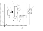
- FIG. 1 is a circuit diagram showing a configuration of a drive circuit for a power semiconductor element in the first embodiment for carrying out the present invention.
- a drive circuit 100 for a power semiconductor element includes a control circuit 3, a MOSFET for turning on (Metal Oxide Field Effect Transistor) 4, a MOSFET for turning off 5, gate resistors 6 and 7, a first DC power supply 8, and a second DC power supply 8.
- the drive circuit 100 is connected to an IGBT 1 that is a power semiconductor element.
- the IGBT 1 includes diodes connected in parallel.
- the control circuit 3 controls on / off of the IGBT 1 that is a power semiconductor element, and controls the on-MOSFET 4 and the off-MOSFET 5 according to the control signal 2 from the outside.
- the on MOSFET 4 is connected to the gate of the IGBT 1 through the gate resistor 6, and the off MOSFET 5 is connected to the gate of the IGBT 1 through the gate resistor 7.
- a charge / discharge current flows through the gate resistor 6 to the gate of the IGBT 1 to turn on the IGBT 1.
- the control circuit 3 turns off the on MOSFET 4 and turns on the off MOSFET 5
- a charge / discharge current flows through the gate resistor 7 to the gate of the IGBT 1 to turn off the IGBT 1.
- the first DC power supply 8 and the second DC power supply 9 constitute a DC power supply that supplies a voltage between the control terminals of the IGBT 1.
- the first DC power supply 8 supplies a positive voltage between the gate and the emitter between the control terminals of the IGBT 1 when the IGBT 1 is in the ON state
- the second DC power supply 9 is connected between the control terminals of the IGBT 1 with the IGBT 1 in the OFF state.
- a negative voltage is supplied between a gate and an emitter.
- the second DC power supply 9 is connected to the emitter of the IGBT 1.
- the ON MOSFET 4 is turned OFF and the OFF MOSFET 5 is turned ON by the control circuit 3.
- a negative voltage ⁇ Ve is applied between the ⁇ emitters by the power supply voltage Ve of the second DC power supply 9.
- a dV / dt malfunction prevention circuit 10 is connected between the gate and emitter of the IGBT 1.
- the dV / dt malfunction prevention circuit 10 includes a normally-on element n-channel JFET (Junction Field Effect Transistor) 11 and a diode provided to prevent reverse current from flowing from the emitter side to the gate side of the IGBT 1. 12.
- the JFET 11 is a switching element connected between the gate and emitter of the IGBT 1 (between the control terminals of the power semiconductor element).
- the gate (control terminal) of the JFET 11 is connected to the GND of the drive circuit 100 on the negative side of the second DC power supply 9, the source of the JFET 11 is connected to the emitter of the IGBT 1, and the drain of the JFET 11 is connected to the IGBT 1 through the diode 12. Connected to the gate.
- the diode 12 is connected in series to the JFET 11 and is connected between the gate and emitter of the IGBT 1.
- the anode of the diode 12 is connected to the gate of the IGBT 1, and the cathode of the diode 12 is connected to the JFET 11.
- the operation of the drive circuit 100 will be described.
- a normal state that is, in a state where the power supply voltage of the second DC power supply 9 is established
- the voltage fluctuation dV / dt is applied to the IGBT 1 during, for example, a recovery operation of a diode connected in parallel to the IGBT 1 during the OFF period of the IGBT 1.
- the negative voltage ⁇ Ve is applied between the gate and the emitter of the IGBT 1.
- the gate-emitter voltage of the IGBT 1 is increased, the gate-emitter voltage is suppressed to be equal to or lower than the threshold voltage of the IGBT 1, so that the IGBT 1 is not turned on by mistake.
- a negative voltage ⁇ Ve is applied between the gate and source of JFET 11, and the absolute value
- the JFET 11 is turned off, and no current flows through the dV / dt malfunction prevention circuit 10. For this reason, the switching operation of the IGBT 1 in a normal state is not affected.
- of the negative voltage ⁇ Ve applied between the gate and the emitter of the IGBT 1 decreases.
- of the threshold voltage Vgs (off) of the JFET 11 the JFET 11 is turned on. That is, the JFET 11 is turned on when the power supply voltage of the second DC power supply 9 which is a DC power supply is lowered. As a result, the JFET 11 short-circuits between the gate and the emitter of the IGBT 1.
- the power semiconductor element drive circuit of the present invention it is not necessary to provide a separate drive circuit or power source for driving the JFET 11, and a simple circuit configuration suppresses the malfunction of the IGBT 1 due to the voltage fluctuation dV / dt. can do. Moreover, since no current flows in the dV / dt malfunction prevention circuit 10 including the JFET 11 at the normal time, the power consumption of the drive circuit 100 can be suppressed. Further, when the power supply voltage of the second DC power supply 9 decreases and the absolute value
- the circuit configuration of the dV / dt malfunction prevention circuit 10 shown in the present embodiment is merely an example, as long as the malfunction prevention function due to the voltage fluctuation dV / dt is satisfied, the JFET 11 can be used in multiple parallels, or for current limitation.
- a resistor having a low impedance that does not cause the IGBT 1 to malfunction even by application of the voltage fluctuation dV / dt may be connected to the gate or drain of the JFET 11.
- the JFET 11 is used as a normally-on element. However, it may be replaced with, for example, a depletion type MOSFET as long as the function is satisfied.
- FIG. FIG. 2 is a circuit diagram showing a configuration of a power semiconductor element drive circuit according to the second embodiment for carrying out the present invention.
- the drive circuit for the power semiconductor element of this embodiment is different from that of Embodiment 1 in that the dV / dt malfunction prevention circuit includes a current amplification stage.
- the current amplifying stage amplifies the source current of the JFET in response to a case where the gate capacity of the power semiconductor element is large and the current capacity of the normally-on JFET is insufficient, and a dV / dt malfunction prevention circuit
- This is an amplifier circuit that increases the current flowing through the. 2
- the same reference numerals as those in FIG. 1 denote the same or corresponding parts, and this is common throughout the entire specification.
- the aspect of the component which appears in the whole specification is an illustration to the last, and is not limited to these description.
- the gate of the JFET 11 that is a normally-on element is connected to the GND of the drive circuit 110, and the drain of the JFET 11 is connected to the gate of the IGBT 1 through the diode 12. Is the same as in the first embodiment.
- the dV / dt malfunction prevention circuit 30 is additionally provided with a current amplification npn transistor 13, a diode 14, and a resistor 15 that constitute an amplifier circuit.
- the npn transistor 13 is a normally-off switching element that is connected between the gate and emitter of the IGBT 1 and amplifies the current flowing through the JFET 11.
- the source of JFET 11 is connected to the emitter of IGBT 1 through resistor 15.
- the source of the JFET 11 is also connected to the base that is the control terminal of the current amplification npn transistor 13.
- the emitter of npn transistor 13 is connected to the emitter of IGBT 1, and the collector of npn transistor 13 is connected to the gate of IGBT 1 via diode 14.
- the JFET 11 When the absolute value
- voltage fluctuation dV / dt is applied to IGBT 1 in this state, the gate voltage of IGBT 1 rises, a current flows through the base of npn transistor 13, and npn transistor 13 is turned on. That is, the npn transistor 13 is turned on when the gate voltage, which is the voltage between the control terminals of the IGBT 1, rises while the power supply voltage of the second DC power supply 9, which is a DC power supply, is lowered.
- the gate-emitter of the IGBT 1 is short-circuited, an increase in the gate voltage of the IGBT 1 is suppressed, and a malfunction in which the IGBT 1 is erroneously turned on can be prevented.
- the npn transistor 13 Since the npn transistor 13 is provided, the current flowing through the dV / dt malfunction prevention circuit 30 is amplified as compared with the dV / dt malfunction prevention circuit 10 shown in the first embodiment. Therefore, even when the gate capacitance of the IGBT 1 is large. , The malfunction of the IGBT 1 can be prevented. Note that the absolute value
- of the base-emitter voltage Vbe of the npn transistor 13 is set to the threshold value Vgs (off of the JFET 11). ) Is set lower than the absolute value
- the npn transistor 13 is used as a current amplification transistor, but an n-channel MOSFET may be used.
- of the threshold voltage Vth between the gate and the source of the MOSFET is set to be lower than the absolute value
- the configuration of the dV / dt malfunction prevention circuit 30 described in the present embodiment is an example for amplifying the source current of the JFET 11, and it is sufficient that the dV / dt malfunction prevention circuit satisfies the function.
- the JFET 11 and the npn transistor 13 may be used in parallel, the npn transistor 13 may be connected in Darlington, and the gate and drain of the JFET 11 and the collector and base of the npn transistor 13 are used for current limiting.
- a resistor may be connected.
- the current is amplified by the npn transistor 13 and the like, so that the control terminal (gate terminal) of the IGBT 1 Even when the JFET 11 alone is insufficient and the current capacity is insufficient, it is possible to prevent a malfunction in which the IGBT 1 is erroneously turned on.
- FIG. 3 is a circuit diagram showing the configuration of the drive circuit for the power semiconductor element according to the third embodiment for carrying out the present invention.
- the drive circuit for the power semiconductor element of this embodiment is different from that of Embodiment 2 in that a pnp transistor is provided as a current amplification transistor of the dV / dt malfunction prevention circuit.
- the dV / dt malfunction prevention circuit 40 is provided with a current amplification pnp transistor 16, a diode 14, and a resistor 15 that constitute an amplifier circuit.
- the gate of the JFET 11 that is a normally-on element is connected to the GND of the drive circuit 120, the source of the JFET 11 is connected to the emitter of the IGBT 1, and the drain of the JFET 11 is a resistor 15 And connected to the gate of the IGBT 1 via the diode 12.
- the drain of the JFET 11 is also connected to the base that is the control terminal of the pnp transistor 16.
- the pnp transistor 16 is a normally-off switching element that is connected between the gate and emitter of the IGBT 1 and amplifies the current flowing through the JFET 11.
- the emitter of the pnp transistor 16 is connected to the gate of the IGBT 1 via the diode 14, and the collector of the pnp transistor 16 is connected to the emitter of the IGBT 1.
- the anode of the diode 12 is connected to the gate of the IGBT 1, but the anode of the diode 12 is connected to the positive side of the first DC power supply 8 or the diode 12 is not installed.
- the resistor 15 may be connected to the positive electrode side of the first DC power supply 8.
- the collector of the pnp transistor 16 is connected to the emitter of the IGBT 1, the collector of the pnp transistor 16 may be connected to the GND of the drive circuit 120.
- the pnp transistor 16 Since the pnp transistor 16 is provided, the current flowing through the dV / dt malfunction prevention circuit 40 is amplified as compared with the dV / dt malfunction prevention circuit 10 shown in the first embodiment. Therefore, even when the gate capacitance of the IGBT 1 is large. , The malfunction of the IGBT 1 can be prevented.
- the feature of using the pnp transistor 16 instead of the npn transistor as a current amplification transistor will be described.
- the base-emitter voltage of the npn transistor is also applied between the source and gate of the JFET 11, so that the threshold voltage Vgs ( off)) must be set higher than the absolute value
- the voltage applied between the gate and source of the JFET 11 is only the negative voltage ⁇ Ve due to the power supply voltage of the second DC power supply 9.
- of the threshold voltage Vgs (off) is changed to the absolute value
- of the threshold voltage Vgs (off) of the JFET 11 is obtained from the absolute value
- the configuration of the dV / dt malfunction prevention circuit 40 described in the present embodiment is an example for amplifying the source current of the JFET 11, and it is sufficient that the dV / dt malfunction prevention circuit satisfies the function.
- the JFET 11 and the pnp transistor 16 may be used in parallel, the pnp transistor 16 may be Darlington connected, and the gate and drain of the JFET 11 and the collector and base of the pnp transistor 16 are used for current limiting.
- a resistor may be connected.
- the current is amplified by the pnp transistor 16 and the like, so that the control terminal (gate terminal) of the IGBT 1 Even when the JFET 11 alone is insufficient and the current capacity is insufficient, it is possible to prevent a malfunction in which the IGBT 1 is erroneously turned on.
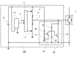
- FIG. 4 is a circuit diagram showing a configuration of a drive circuit for a power semiconductor element in the fourth embodiment for carrying out the present invention.
- the drive circuit for the power semiconductor element of this embodiment is different from that of Embodiment 1 in that it includes a power supply voltage detection circuit.
- the IGBT1 when the power supply voltage of the DC power supply in the drive circuit is reduced due to a power failure or the like, the IGBT1 is connected by short-circuiting the gate-emitter of the IGBT1 using a JFET, a transistor, or a MOSFET. It prevents the malfunction that turns on accidentally. However, a power failure or the like may occur when the IGBT 1 is turned on, and the power supply voltage of the DC power supply may be lowered. In this case, if the dV / dt malfunction prevention circuit operates faster than turning off the IGBT 1 via the gate resistor, there is a possibility that the gate-emitter of the IGBT 1 is short-circuited and the IGBT 1 is rapidly turned off.
- the power semiconductor element drive circuit has a function of normally turning off the IGBT 1 before the dV / dt malfunction prevention circuit operates.
- a power supply voltage detection circuit 17 is added to the power semiconductor element drive circuit 130 in addition to the power semiconductor element drive circuit 100 described in the first embodiment. Even if the dV / dt malfunction prevention circuit other than those shown in the first to third embodiments has a function of suppressing an increase in the gate voltage of the IGBT in a state where the power supply voltage of the DC power supply is lowered, for example, no Even in a circuit using a normally-off element without using a marly-on element, the function of avoiding rapid IGBT turn-off is satisfied.
- the power supply voltage detection circuit 17 is composed of, for example, a comparator and is connected to the positive side of the second DC power supply 9 in order to detect the power supply voltage of the second DC power supply 9.
- the voltage detection level of the power supply voltage detection circuit 17 is set so that a voltage drop can be detected when the power supply voltage of the second DC power supply 9 drops by ⁇ V.
- ⁇ V is a predetermined power supply voltage drop detected by the power supply voltage detection circuit 17.
- the voltage detection level of the power supply voltage detection circuit 17 is set higher than the voltage at which the dV / dt malfunction prevention circuit 10 starts to operate.
- the power supply voltage detection circuit 17 goes to the control circuit 3.
- the off signal is output, and the control circuit 3 controls the on MOSFET 4 and the off MOSFET 5 to turn off the IGBT 1 or maintain the IGBT 1 in the off state. Since such an operation is performed, the IGBT 1 can be normally turned off before the dV / dt malfunction prevention circuit 10 operates even when the power supply voltage of the second DC power supply 9 decreases due to a power failure or the like.
- of the threshold voltage Vgs (off) of the JFET 11 is
- the voltage detection level is set so as to satisfy the relationship of Vgs
- the difference between the power supply voltage Ve and the threshold voltage Vgs (off) at which the JFET 11 serving as the switching element is turned on is the amount of decrease in the power supply voltage of the second DC power supply 9 at which the JFET 11 is turned on.
- means that the power supply voltage decrease amount of the second DC power supply 9 in which the JFET 11 is turned on is equal to the predetermined power supply voltage decrease amount detected by the power supply voltage detection circuit 17. To make it smaller.
- the power supply voltage detection circuit 17 detects a decrease in the power supply voltage of the second DC power supply 9. Then, the power supply voltage detection circuit 17 outputs an off command to the control circuit 3, and the control circuit 3 turns off the IGBT 1.
- the power supply voltage of the second DC power supply 9 decreases to the threshold voltage Vgs (off) of the JFET 11
- the JFET 11 is turned on, and the gate voltage of the IGBT 1 increases even when the voltage fluctuation dV / dt is applied. Suppress.
- the power supply voltage detection circuit 17 detects a drop in the power supply voltage of the second DC power supply 9.
- the power supply voltage detection circuit 17 is connected to the positive side of the first DC power supply 8, and the first DC power supply 8 and the second DC power supply 9 are connected.
- a drop in the power supply voltage may be detected.
- the power supply voltage detection circuit 17 detects the voltage drop of the power supply voltage and before the IGBT 1 is turned off, the voltage detection level of the power supply voltage detection circuit 17 and the dV / dt are set so that the dV / dt malfunction prevention circuit 10 does not operate.
- a voltage at which the dt malfunction prevention circuit 10 starts to operate (for example, the threshold voltage Vge (off) of the JFET 11) is set.
- the dV / dt malfunction prevention circuit 10 may be set not to operate first. it can.
- the power supply voltage detection circuit 17 detects when the power supply voltage of the first DC power supply 8 and the second DC power supply 9 decreases by ⁇ V.
- the voltage detection level “Ve ⁇ V” is set so as to satisfy the relationship of
- the rate of reduction between the first DC power source 8 and the second DC power source 9 may be determined.
- the setting range of the voltage detection level of the voltage detection circuit 17 and the threshold voltage Vgs (off) of the JFET 11 may be widened.
- the power supply voltage detection circuit 17 shown in the present embodiment is also added to the second and third embodiments. An effect can also be obtained.
- the power supply voltage detection circuit 17 that detects a decrease in the voltage supplied from at least one of the first DC power supply 8 and the second DC power supply 9 is provided. Even when the power supply voltage of the DC power supply of the drive circuit 130 is reduced due to a power failure or the like, the power semiconductor element can be normally turned off by the power supply voltage detection circuit 17 before the switching element is turned on. It can prevent turning off at high speed.
- FIG. FIG. 6 is a circuit diagram showing a configuration of a drive circuit for a power semiconductor element in the fifth embodiment for carrying out the present invention.
- the drive circuit for the power semiconductor element of this embodiment is different from that of the fourth embodiment in that a normally-off element is used instead of a normally-on element in the dV / dt malfunction prevention circuit.
- the dV / dt malfunction prevention circuit 50 using the normally-off element includes a power supply of the second DC power supply 9 between the base and emitter of the first npn transistor 18, the second npn transistor 19, and the first npn transistor 18.
- the resistors 20 and 21 for dividing and inputting the voltage are connected in series between the gate and the emitter of the IGBT 1, and the collector of the first npn transistor 18 and the base of the second npn transistor 19 are connected to the connection point.
- the resistors 22 and 23 are provided.
- the drive circuit 150 In a normal state, that is, in a state where the power supply voltage of the second DC power supply 9 is established, the power supply voltage of the second DC power supply 9 is divided by resistors 20 and 21 between the base and emitter of the first npn transistor 18. The pressed voltage is applied, and the first npn transistor 18 is turned on. When the first npn transistor 18 is turned on, the base voltage of the second npn transistor 19 becomes a voltage equivalent to the GND of the drive circuit 150, the second npn transistor 19 is turned off, and normal switching operation of the IGBT 1 is performed. Does not affect.
- the voltage detection level of the power supply voltage detection circuit 17 is set higher than the threshold value of the dV / dt malfunction prevention circuit 50.
- the detection circuit 17 operates to turn off or maintain the IGBT 1.
- the power supply voltage of the second DC power supply 9 further decreases, the base-emitter voltage of the first npn transistor 18 decreases and the first npn transistor 18 is turned off.
- the voltage fluctuation dV / dt is applied and the gate voltage of the IGBT 1 rises, a current flows through the resistor 22 to the base of the second npn transistor 19 and the second npn transistor 19 is turned on.
- the second npn transistor 19 When the second npn transistor 19 is turned on, the gate-emitter of the IGBT 1 is short-circuited, and an increase in the gate voltage of the IGBT 1 can be suppressed. That is, the second npn transistor 19 is turned on when the gate voltage, which is the voltage between the control terminals of the IGBT 1, increases a predetermined power supply voltage decrease amount detected by the power supply voltage detection circuit 17 as in the fourth embodiment. The amount of decrease in the power supply voltage of the second DC power supply 9 is made smaller.
- a reverse current may flow through the second npn transistor 19.
- the second npn transistor 19 and the IGBT 1 A reverse current preventing diode may be inserted between the gate and the gate. The reverse current preventing diode is inserted so that the cathode is on the second npn transistor 19 side.
- the configuration of the dV / dt malfunction prevention circuit 50 described in the present embodiment is merely an example, and the dV / dt malfunction prevention circuit only needs to satisfy the function, and the second npn depends on the required current capacity.
- the transistors 19 may be used in multiple parallels, the second npn transistor 19 may be Darlington-connected, and a current limiting resistor is provided to the gate and drain of the JFET 11 and the collector and base of the second npn transistor 19. You may connect.
- the first npn transistor 18 when the first npn transistor 18 is in an on state and the IGBT 1 is also in an on state during normal operation, current continues to flow through the resistor 22. For this reason, in order to suppress the power consumption of the resistor 22, it is necessary to increase the resistance value of the resistor 22. Accordingly, since the base current of the second npn transistor 19 is reduced, it is effective to connect the second npn transistor 19 to the Darlington connection. Further, although an npn transistor is used in this embodiment, an n-channel MOSFET may be used instead of the npn transistor.
- FIG. 6 shows an example in which the power supply voltage detection circuit 17 detects a decrease in the power supply voltage of the second DC power supply 9.
- the power supply voltage detection circuit 17 is replaced with the first power supply voltage detection circuit 17. It may be connected between the positive electrode side of one DC power supply 8 and the GND of the drive circuit 150 to detect a voltage drop of the power supply voltage of the first DC power supply 8 and the second DC power supply 9 combined. Even in this case, the power supply voltage detection circuit 17 detects the voltage drop of the power supply voltage, and before the IGBT 1 is turned off, the voltage detection level of the power supply voltage detection circuit 17 and the dV / dt are set so that the dV / dt malfunction prevention circuit 50 does not operate. The voltage at which the dt malfunction prevention circuit 50 starts to operate is set.
- the first and second npn transistors 18 and 19 which are normally-off elements are used in the dV / dt malfunction prevention circuit 50, malfunction of the IGBT 1 can be suppressed with a simple circuit configuration.
- the power supply voltage detection circuit 17 is provided, the normally-off element of the dV / dt malfunction prevention circuit 50 can be used even when the power supply voltage of the DC power supply of the drive circuit 150 is reduced due to a power failure or the like during the ON period of the IGBT 1. Since the power semiconductor element can be normally turned off before turning on, it is possible to prevent the power semiconductor element from being turned off at high speed.
- FIG. FIG. 7 is a circuit diagram showing a configuration of a drive circuit for a power semiconductor element according to the sixth embodiment for carrying out the present invention.
- the drive circuit for the power semiconductor element of the present embodiment is that the DC power supply is composed of only the first DC power supply that supplies a positive voltage between the gate and emitter between the control terminals of the IGBT 1. And different.
- the present embodiment is applied when the power semiconductor element does not malfunction even if a negative voltage is not applied between the gate and the emitter in the off state, such as when the voltage fluctuation dV / dt between the collector and the emitter is small. is there.
- the power supply voltage detection circuit 17 is connected to the positive side of the first DC power supply 8 to detect a voltage drop of the first DC power supply 8.
- the resistor 20 is connected not to the negative side of the first DC power supply 8 but to the positive side of the first DC power supply 8.
- the dV / dt malfunction prevention circuit 60 using a normally-off element includes a power supply of the first DC power supply 8 between the base and emitter of the first npn transistor 18, the second npn transistor 19, and the first npn transistor 18.
- the resistors 20 and 21 for dividing and inputting the voltage are connected in series between the gate and the emitter of the IGBT 1, and the collector of the first npn transistor 18 and the base of the second npn transistor 19 are connected to the connection point.
- the resistors 22 and 23 are provided.
- the drive circuit 160 In a normal state, that is, in a state where the power supply voltage of the first DC power supply 8 is established, the power supply voltage of the first DC power supply 8 is resisted via the resistor 20 connected to the positive side of the first DC power supply 8.
- the voltage divided by 20 and 21 is applied between the base and emitter of the first npn transistor 18, and the first npn transistor 18 is turned on.
- the collector-emitter voltage of the first npn transistor 18 to be lower than the base-emitter voltage at which the second npn transistor 19 is turned on, the second npn transistor 19 is turned off.
- the normal switching operation of the IGBT 1 is not affected.
- the voltage detection level of the power supply voltage detection circuit 17 is set higher than the threshold value of the dV / dt malfunction prevention circuit 60.
- the detection circuit 17 operates to turn off or maintain the IGBT 1.
- the power supply voltage of the first DC power supply 8 further decreases, the base-emitter voltage of the first npn transistor 18 decreases and the first npn transistor 18 is turned off.
- a current flows through the resistor 22 to the base of the second npn transistor 19 and the second npn transistor 19 is turned on.
- the second npn transistor 19 is turned on, the gate-emitter of the IGBT 1 is short-circuited, and an increase in the gate voltage of the IGBT 1 can be suppressed.
- a reverse current may flow through the second npn transistor 19.
- the second npn transistor 19 and the IGBT 1 A reverse current preventing diode may be inserted between the gate and the gate. The reverse current preventing diode is inserted so that the cathode is on the second npn transistor 19 side.
- the configuration of the dV / dt malfunction prevention circuit 60 described in the present embodiment is an example, and the dV / dt malfunction prevention circuit only needs to satisfy the function, and the second npn depends on the required current capacity.
- the transistors 19 may be used in multiple parallels, the second npn transistor 19 may be Darlington-connected, and a current limiting resistor is provided to the gate and drain of the JFET 11 and the collector and base of the second npn transistor 19. You may connect.
- the first and second npn transistors 18 and 19, which are normally-off elements, are used in the dV / dt malfunction prevention circuit 60 even if the DC power source is configured by only the first DC power source 1.
- the malfunction of the IGBT 1 can be suppressed with a simple circuit configuration.
- the normally-off element of the dV / dt malfunction prevention circuit 60 can be used even when the power supply voltage of the DC power supply of the drive circuit 160 is reduced due to a power failure or the like during the ON period of the IGBT 1. Since the power semiconductor element can be normally turned off before turning on, it is possible to prevent the power semiconductor element from being turned off at high speed.
- the IGBT is used as the power semiconductor element.
- the power semiconductor element shown in all the embodiments is applied to a voltage-driven power semiconductor element such as a MOSFET.
- a drive circuit can be applied.
- the drive circuits described in all the embodiments can be applied not only to Si but also to a wide gap semiconductor such as SiC. Note that a wide gap semiconductor such as SiC may have a low threshold voltage Vth and is likely to malfunction. Therefore, for power semiconductor elements manufactured using SiC or the like, the drive circuits described in all the embodiments are used. The effect that it can be used to prevent malfunction is further increased.
- 1 IGBT power semiconductor element
- 2 control signal 3 control circuit
- 4 on MOSFET 5 off MOSFET
- 6 gate resistance 8 first DC power supply
- 9 second DC power supply 10, 30 , 40, 50, 60 dV / dt malfunction prevention circuit, 11 JFET, 12, 14 diode, 13 npn transistor, 15, 20-23 resistor, 16 pnp transistor, 17 power supply voltage detection circuit, 18 first npn transistor, 19 Second npn transistor, 100, 110, 120, 130, 140, 150, 160 drive circuit.
Landscapes
- Engineering & Computer Science (AREA)
- Power Engineering (AREA)
- Power Conversion In General (AREA)
- Electronic Switches (AREA)
Abstract
Description
図1は、この発明を実施するための実施の形態1における電力用半導体素子の駆動回路の構成を示す回路図である。図1において、電力用半導体素子の駆動回路100は、制御回路3、オン用MOSFET(Metal Oxide Semiconductor Field Effect Transistor)4、オフ用MOSFET5、ゲート抵抗6,7、第一の直流電源8、第二の直流電源9、dV/dt誤動作防止回路10によって構成されている。駆動回路100には、電力用半導体素子であるIGBT1が接続されている。IGBT1は、並列接続されたダイオードを備えている。
図2は、この発明を実施するための実施の形態2における電力用半導体素子の駆動回路の構成を示す回路図である。本実施の形態の電力用半導体素子の駆動回路は、dV/dt誤動作防止回路に電流増幅段を備えた点が実施の形態1と異なる。電流増幅段は、電力用半導体素子のゲート容量が大きく、ノーマリーオン素子であるJFETの電流容量が不足するような場合に対応して、JFETのソース電流を増幅し、dV/dt誤動作防止回路に流れる電流を大きくする増幅回路である。図2において、図1と同一の符号を付したものは、同一またはこれに相当するものであり、このことは明細書の全文において共通することである。また、明細書全文に表れている構成要素の態様は、あくまで例示であってこれらの記載に限定されるものではない。
図3は、この発明を実施するための実施の形態3における電力用半導体素子の駆動回路の構成を示す回路図である。本実施の形態の電力用半導体素子の駆動回路は、dV/dt誤動作防止回路の電流増幅用のトランジスタとしてpnpトランジスタを備えた点が実施の形態2と異なる。dV/dt誤動作防止回路40には、増幅回路を構成する電流増幅用のpnpトランジスタ16、ダイオード14、および抵抗15が設けられている。
図4は、この発明を実施するための実施の形態4における電力用半導体素子の駆動回路の構成を示す回路図である。本実施の形態の電力用半導体素子の駆動回路は、電源電圧検知回路を備えた点が実施の形態1と異なる。
図6は、この発明を実施するための実施の形態5における電力用半導体素子の駆動回路の構成を示す回路図である。本実施の形態の電力用半導体素子の駆動回路は、dV/dt誤動作防止回路にノーマリーオン素子の代わりにノーマリーオフ素子を用いた点が実施の形態4と異なる。
図7は、この発明を実施するための実施の形態6における電力用半導体素子の駆動回路の構成を示す回路図である。本実施の形態の電力用半導体素子の駆動回路は、直流電源がIGBT1の制御端子間であるゲート-エミッタ間に正電圧を供給する第一の直流電源のみで構成される点が実施の形態5と異なる。本実施の形態はコレクタ-エミッタ間の電圧変動dV/dtが小さい場合等、オフ状態でゲート-エミッタ間に負電圧を印加しなくても電力用半導体素子が誤動作しない場合に適用されるものである。
Claims (10)
- 電力用半導体素子のオンオフを制御する制御回路と、
前記電力用半導体素子の制御端子間に電圧を供給する直流電源と、
前記電力用半導体素子の制御端子間に接続されたスイッチング素子とを備え、
前記スイッチング素子は、前記直流電源の電源電圧が低下した場合にオンし、または、前記直流電源の電源電圧が低下した状態で前記電力用半導体素子の制御端子間電圧が上昇した場合にオンし、前記電力用半導体素子の制御端子間を短絡させることを特徴とする電力用半導体素子の駆動回路。 - 前記直流電源は、前記電力用半導体素子がオン状態で前記電力用半導体素子の制御端子間に正電圧を供給する第一の直流電源と、前記電力用半導体素子がオフ状態で前記電力用半導体素子の制御端子間に負電圧を供給する第二の直流電源とによって構成され、
前記スイッチング素子は、前記第二の直流電源の電源電圧が低下した場合にオンし、または、前記第二の直流電源の電源電圧が低下した状態で前記電力用半導体素子の制御端子間電圧が上昇した場合にオンし、前記電力用半導体素子の制御端子間を短絡させることを特徴とする請求項1に記載の電力用半導体素子の駆動回路。 - 前記直流電源の電源電圧の低下を検知し、前記直流電源の電源電圧が所定の電源電圧低下量に達した場合に前記電力用半導体素子をオフする信号を前記制御回路へ出力する電源電圧検知回路を備え、
前記所定の電源電圧低下量を前記スイッチング素子がオンする前記直流電源の電源電圧の低下量より小さく、または、前記所定の電源電圧低下量を前記電力用半導体素子の制御端子間電圧が上昇した場合に前記スイッチング素子がオンする前記直流電源の電源電圧の低下量より小さくしたことを特徴とする請求項1に記載の電力用半導体素子の駆動回路。 - 前記スイッチング素子は、ノーマリーオン素子であることを特徴とする請求項1に記載の電力用半導体素子の駆動回路。
- 前記スイッチング素子は、ノーマリーオン素子であり、
前記スイッチング素子の制御端子は、前記第二の直流電源の負極側に接続されたことを特徴とする請求項2に記載の電力用半導体素子の駆動回路。 - 前記スイッチング素子は、ノーマリーオフ素子であることを特徴とする請求項1に記載の電力用半導体素子の駆動回路。
- 前記電力用半導体素子の制御端子間に接続され、前記スイッチング素子に流れる電流を増幅する増幅回路を備えたことを特徴とする請求項1に記載の電力用半導体素子の駆動回路。
- 前記電力用半導体素子の制御端子間に前記スイッチング素子と直列にダイオードが挿入され、
前記ダイオードは、アノード側が前記電力用半導体素子のゲート端子側となるように接続されたことを特徴とする請求項1に記載の電力用半導体素子の駆動回路。 - 前記スイッチング素子のしきい値電圧の絶対値を、前記第二の直流電源の正常時の前記負電圧の絶対値より低く設定したことを特徴とする請求項2に記載の電力用半導体素子の駆動回路。
- 前記電力用半導体素子は、SiC半導体であることを特徴とする請求項1に記載の電力用半導体素子の駆動回路。
Priority Applications (7)
| Application Number | Priority Date | Filing Date | Title |
|---|---|---|---|
| KR1020127021588A KR101217357B1 (ko) | 2008-08-21 | 2009-07-22 | 전력용 반도체 소자의 구동 회로 |
| KR1020117003761A KR101313498B1 (ko) | 2008-08-21 | 2009-07-22 | 전력용 반도체 소자의 구동 회로 |
| CN200980140608.1A CN102187557B (zh) | 2008-08-21 | 2009-07-22 | 功率用半导体元件的驱动电路 |
| EP09808018.7A EP2320544B1 (en) | 2008-08-21 | 2009-07-22 | Driving circuit for power semiconductor element |
| JP2010525568A JP5293740B2 (ja) | 2008-08-21 | 2009-07-22 | 電力用半導体素子の駆動回路 |
| US13/059,429 US9806593B2 (en) | 2008-08-21 | 2009-07-22 | Drive circuit of power semiconductor device |
| CA2734701A CA2734701C (en) | 2008-08-21 | 2009-07-22 | Drive circuit of power semiconductor device |
Applications Claiming Priority (2)
| Application Number | Priority Date | Filing Date | Title |
|---|---|---|---|
| JP2008212614 | 2008-08-21 | ||
| JP2008-212614 | 2008-08-21 |
Publications (1)
| Publication Number | Publication Date |
|---|---|
| WO2010021082A1 true WO2010021082A1 (ja) | 2010-02-25 |
Family
ID=41706975
Family Applications (1)
| Application Number | Title | Priority Date | Filing Date |
|---|---|---|---|
| PCT/JP2009/003419 WO2010021082A1 (ja) | 2008-08-21 | 2009-07-22 | 電力用半導体素子の駆動回路 |
Country Status (7)
| Country | Link |
|---|---|
| US (1) | US9806593B2 (ja) |
| EP (1) | EP2320544B1 (ja) |
| JP (2) | JP5293740B2 (ja) |
| KR (2) | KR101313498B1 (ja) |
| CN (1) | CN102187557B (ja) |
| CA (1) | CA2734701C (ja) |
| WO (1) | WO2010021082A1 (ja) |
Cited By (8)
| Publication number | Priority date | Publication date | Assignee | Title |
|---|---|---|---|---|
| JP2012034079A (ja) * | 2010-07-29 | 2012-02-16 | Fuji Electric Co Ltd | 絶縁ゲート型デバイスの駆動回路 |
| WO2014041666A1 (ja) * | 2012-09-13 | 2014-03-20 | 三菱電機株式会社 | 半導体装置とその半導体装置を用いた自動車 |
| JP2014112925A (ja) * | 2014-02-07 | 2014-06-19 | Fuji Electric Co Ltd | 絶縁ゲート型デバイスの駆動回路 |
| WO2015182658A1 (ja) * | 2014-05-30 | 2015-12-03 | 三菱電機株式会社 | 電力用半導体素子の駆動回路 |
| EP3174201A1 (en) * | 2010-10-21 | 2017-05-31 | Atmel Corporation | Switch used in programmable gain amplifier and programmable gain amplifier |
| JPWO2017086113A1 (ja) * | 2015-11-17 | 2017-11-16 | 株式会社オートネットワーク技術研究所 | スイッチ回路及び電源システム |
| JPWO2018186353A1 (ja) * | 2017-04-05 | 2020-02-20 | ローム株式会社 | パワーモジュール |
| JP7559716B2 (ja) | 2021-09-07 | 2024-10-02 | 三菱電機株式会社 | 半導体装置 |
Families Citing this family (22)
| Publication number | Priority date | Publication date | Assignee | Title |
|---|---|---|---|---|
| JP5840975B2 (ja) * | 2012-02-22 | 2016-01-06 | 三菱電機株式会社 | ゲート駆動回路 |
| CN103532353B (zh) * | 2013-10-25 | 2015-10-28 | 山东大学 | 具有高负电压的自举供电mosfet/igbt驱动线路 |
| US11070046B2 (en) * | 2014-09-11 | 2021-07-20 | Mitsubishi Electric Corporation | Short-circuit protection circuit for self-arc-extinguishing type semiconductor element |
| CN105576945B (zh) * | 2014-10-11 | 2018-11-16 | 台达电子工业股份有限公司 | 隔离电源控制装置、电源变换装置及其隔离电源控制方法 |
| JP6583284B2 (ja) * | 2014-11-06 | 2019-10-02 | 富士電機株式会社 | 半導体素子の駆動装置 |
| CN104506028B (zh) * | 2015-01-13 | 2017-05-10 | 山东大学 | 一种SiC MOSFET半桥电路驱动器以及半桥电路驱动方法 |
| JP6638504B2 (ja) * | 2016-03-22 | 2020-01-29 | アイシン・エィ・ダブリュ株式会社 | インバータ駆動装置 |
| WO2018047561A1 (ja) * | 2016-09-09 | 2018-03-15 | 富士電機株式会社 | 電力素子の駆動回路 |
| CN108631761A (zh) * | 2017-03-16 | 2018-10-09 | 佛山市顺德区美的电热电器制造有限公司 | 电磁加热系统以及功率开关管的控制装置和方法 |
| CN107835002B (zh) * | 2017-09-20 | 2024-03-12 | 同方威视技术股份有限公司 | 固态脉冲调制器中的保护电路、振荡补偿电路和供电电路 |
| JP7024463B2 (ja) * | 2018-02-01 | 2022-02-24 | 株式会社Gsユアサ | 管理装置、蓄電装置、蓄電素子の管理方法 |
| EP3544183A1 (de) * | 2018-03-19 | 2019-09-25 | Siemens Aktiengesellschaft | Schaltungsanordnung zum betreiben eines halbleiterschalters |
| CN112166550A (zh) * | 2018-05-28 | 2021-01-01 | 三菱电机株式会社 | 电力变换装置 |
| JP7259430B2 (ja) * | 2018-05-30 | 2023-04-18 | 富士電機株式会社 | 電圧駆動型半導体スイッチング素子のゲート駆動装置、該ゲート駆動装置を備える電力変換装置 |
| CN110798186B (zh) * | 2018-08-01 | 2023-09-08 | 中车株洲电力机车研究所有限公司 | 一种用于功率半导体器件的驱动装置 |
| JP7120139B2 (ja) * | 2019-04-16 | 2022-08-17 | 株式会社デンソー | スイッチの駆動回路 |
| CN110609583A (zh) * | 2019-08-26 | 2019-12-24 | 无锡十顶电子科技有限公司 | 一种用于蜂鸣器稳定驱动管栅极电压的电路 |
| JP7300370B2 (ja) * | 2019-11-05 | 2023-06-29 | 株式会社日立製作所 | 半導体装置の駆動装置および駆動方法、並びに電力変換装置 |
| US11258443B2 (en) * | 2020-06-30 | 2022-02-22 | Apple Inc. | Fast active clamp for power converters |
| JP7528660B2 (ja) * | 2020-09-10 | 2024-08-06 | オムロン株式会社 | 過電流保護回路および電力変換器 |
| CN112769320B (zh) * | 2021-01-04 | 2022-11-29 | 南京博兰得电子科技有限公司 | 钳位开关驱动电路 |
| EP4407871A1 (en) * | 2023-01-24 | 2024-07-31 | Infineon Technologies Austria AG | Electronic circuit with a transistor device and a protection circuit |
Citations (6)
| Publication number | Priority date | Publication date | Assignee | Title |
|---|---|---|---|---|
| JPS6399616A (ja) * | 1986-03-24 | 1988-04-30 | Matsushita Electric Works Ltd | 固体リレ−及びその製造方法 |
| JPH01300617A (ja) * | 1988-05-30 | 1989-12-05 | Fuji Electric Co Ltd | ゲート駆動回路 |
| JPH10257755A (ja) * | 1997-03-13 | 1998-09-25 | Toyota Autom Loom Works Ltd | フォトカップラー駆動のスイッチング回路 |
| JPH10285909A (ja) | 1997-04-11 | 1998-10-23 | Toshiba Fa Syst Eng Kk | 電源自給式のゲート回路 |
| JP2006157367A (ja) * | 2004-11-29 | 2006-06-15 | Sanken Electric Co Ltd | 信号伝達回路 |
| JP2009081962A (ja) * | 2007-09-26 | 2009-04-16 | Sharp Corp | スイッチング回路、回路、並びにスイッチング回路及び駆動パルス生成回路を含む回路 |
Family Cites Families (11)
| Publication number | Priority date | Publication date | Assignee | Title |
|---|---|---|---|---|
| US3819952A (en) * | 1973-01-29 | 1974-06-25 | Mitsubishi Electric Corp | Semiconductor device |
| US4492883A (en) * | 1982-06-21 | 1985-01-08 | Eaton Corporation | Unpowered fast gate turn-off FET |
| US4691129A (en) * | 1986-03-19 | 1987-09-01 | Siemens Aktiengesellschaft | Drive circuit for a power MOSFET with source-side load |
| US4804866A (en) | 1986-03-24 | 1989-02-14 | Matsushita Electric Works, Ltd. | Solid state relay |
| US4748351A (en) * | 1986-08-26 | 1988-05-31 | American Telephone And Telegraph Company, At&T Bell Laboratories | Power MOSFET gate driver circuit |
| US4970420A (en) * | 1989-07-13 | 1990-11-13 | Westinghouse Electric Corp. | Power field effect transistor drive circuit |
| JPH0677797A (ja) | 1992-08-26 | 1994-03-18 | Sansha Electric Mfg Co Ltd | 電力用スイッチング半導体モジュール |
| JPH0715949A (ja) | 1993-06-28 | 1995-01-17 | Fuji Electric Co Ltd | 電力変換装置のゲート駆動回路 |
| JP3421507B2 (ja) * | 1996-07-05 | 2003-06-30 | 三菱電機株式会社 | 半導体素子の駆動回路 |
| US6331794B1 (en) * | 1999-03-10 | 2001-12-18 | Richard A. Blanchard | Phase leg with depletion-mode device |
| FR2911736B1 (fr) | 2007-01-23 | 2009-03-20 | Schneider Toshiba Inverter | Dispositif de commande d'un interrupteur de puissance et variateur comprenant un tel dipositif. |
-
2009
- 2009-07-22 KR KR1020117003761A patent/KR101313498B1/ko active IP Right Grant
- 2009-07-22 US US13/059,429 patent/US9806593B2/en active Active
- 2009-07-22 JP JP2010525568A patent/JP5293740B2/ja active Active
- 2009-07-22 CN CN200980140608.1A patent/CN102187557B/zh active Active
- 2009-07-22 WO PCT/JP2009/003419 patent/WO2010021082A1/ja active Application Filing
- 2009-07-22 KR KR1020127021588A patent/KR101217357B1/ko active IP Right Grant
- 2009-07-22 EP EP09808018.7A patent/EP2320544B1/en active Active
- 2009-07-22 CA CA2734701A patent/CA2734701C/en active Active
-
2013
- 2013-04-18 JP JP2013087701A patent/JP6132640B2/ja active Active
Patent Citations (6)
| Publication number | Priority date | Publication date | Assignee | Title |
|---|---|---|---|---|
| JPS6399616A (ja) * | 1986-03-24 | 1988-04-30 | Matsushita Electric Works Ltd | 固体リレ−及びその製造方法 |
| JPH01300617A (ja) * | 1988-05-30 | 1989-12-05 | Fuji Electric Co Ltd | ゲート駆動回路 |
| JPH10257755A (ja) * | 1997-03-13 | 1998-09-25 | Toyota Autom Loom Works Ltd | フォトカップラー駆動のスイッチング回路 |
| JPH10285909A (ja) | 1997-04-11 | 1998-10-23 | Toshiba Fa Syst Eng Kk | 電源自給式のゲート回路 |
| JP2006157367A (ja) * | 2004-11-29 | 2006-06-15 | Sanken Electric Co Ltd | 信号伝達回路 |
| JP2009081962A (ja) * | 2007-09-26 | 2009-04-16 | Sharp Corp | スイッチング回路、回路、並びにスイッチング回路及び駆動パルス生成回路を含む回路 |
Cited By (13)
| Publication number | Priority date | Publication date | Assignee | Title |
|---|---|---|---|---|
| US8890581B2 (en) | 2010-07-29 | 2014-11-18 | Fuji Electric Co., Ltd. | Driving circuit of insulated gate device |
| JP2012034079A (ja) * | 2010-07-29 | 2012-02-16 | Fuji Electric Co Ltd | 絶縁ゲート型デバイスの駆動回路 |
| EP3174201A1 (en) * | 2010-10-21 | 2017-05-31 | Atmel Corporation | Switch used in programmable gain amplifier and programmable gain amplifier |
| WO2014041666A1 (ja) * | 2012-09-13 | 2014-03-20 | 三菱電機株式会社 | 半導体装置とその半導体装置を用いた自動車 |
| US9742285B2 (en) | 2012-09-13 | 2017-08-22 | Mitsubishi Electric Corporation | Semiconductor device and automobile |
| JP2014112925A (ja) * | 2014-02-07 | 2014-06-19 | Fuji Electric Co Ltd | 絶縁ゲート型デバイスの駆動回路 |
| WO2015182658A1 (ja) * | 2014-05-30 | 2015-12-03 | 三菱電機株式会社 | 電力用半導体素子の駆動回路 |
| JP5989265B2 (ja) * | 2014-05-30 | 2016-09-07 | 三菱電機株式会社 | 電力用半導体素子の駆動回路 |
| US10038438B2 (en) | 2014-05-30 | 2018-07-31 | Mitsubishi Electric Corporation | Power semiconductor element driving circuit |
| JPWO2017086113A1 (ja) * | 2015-11-17 | 2017-11-16 | 株式会社オートネットワーク技術研究所 | スイッチ回路及び電源システム |
| JPWO2018186353A1 (ja) * | 2017-04-05 | 2020-02-20 | ローム株式会社 | パワーモジュール |
| JP7157046B2 (ja) | 2017-04-05 | 2022-10-19 | ローム株式会社 | パワーモジュール |
| JP7559716B2 (ja) | 2021-09-07 | 2024-10-02 | 三菱電機株式会社 | 半導体装置 |
Also Published As
| Publication number | Publication date |
|---|---|
| CA2734701C (en) | 2015-02-17 |
| US20110204929A1 (en) | 2011-08-25 |
| EP2320544B1 (en) | 2019-02-20 |
| CN102187557B (zh) | 2014-12-24 |
| JPWO2010021082A1 (ja) | 2012-01-26 |
| KR20120101595A (ko) | 2012-09-13 |
| US9806593B2 (en) | 2017-10-31 |
| CA2734701A1 (en) | 2010-02-25 |
| KR20110031246A (ko) | 2011-03-24 |
| KR101217357B1 (ko) | 2012-12-31 |
| JP6132640B2 (ja) | 2017-05-24 |
| JP5293740B2 (ja) | 2013-09-18 |
| KR101313498B1 (ko) | 2013-10-01 |
| CN102187557A (zh) | 2011-09-14 |
| EP2320544A1 (en) | 2011-05-11 |
| JP2013179828A (ja) | 2013-09-09 |
| EP2320544A4 (en) | 2015-01-07 |
Similar Documents
| Publication | Publication Date | Title |
|---|---|---|
| JP6132640B2 (ja) | 電力用半導体素子の駆動回路 | |
| JP6197685B2 (ja) | ゲート駆動回路 | |
| JP5776658B2 (ja) | 半導体駆動装置 | |
| US9467138B2 (en) | Semiconductor apparatus | |
| JP6350214B2 (ja) | 駆動装置 | |
| JP5767734B2 (ja) | 電力用半導体装置 | |
| WO2015146040A1 (ja) | 駆動装置 | |
| JP2012090435A (ja) | 駆動回路及びこれを備える半導体装置 | |
| JP4779549B2 (ja) | 電圧駆動型半導体素子のゲート駆動回路。 | |
| JP2017212583A (ja) | 半導体素子の保護回路 | |
| JP2017079534A (ja) | ゲート制御回路 | |
| US9831665B2 (en) | Overcurrent protection circuit | |
| US9568505B2 (en) | Semiconductor device | |
| US9684323B2 (en) | Regulator circuit that suppresses an overshoot of output voltage | |
| US20090066400A1 (en) | Circuit for Switching a Voltage-Controlled Transistor | |
| JP6299416B2 (ja) | 駆動回路システム | |
| JP2016131465A (ja) | ゲート駆動回路 | |
| JP2012080488A (ja) | ゲート駆動回路 | |
| JP2015220932A (ja) | 半導体装置 | |
| JP7566161B2 (ja) | スイッチング素子駆動回路 | |
| JP2022086469A (ja) | 半導体装置 |
Legal Events
| Date | Code | Title | Description |
|---|---|---|---|
| WWE | Wipo information: entry into national phase |
Ref document number: 200980140608.1 Country of ref document: CN |
|
| 121 | Ep: the epo has been informed by wipo that ep was designated in this application |
Ref document number: 09808018 Country of ref document: EP Kind code of ref document: A1 |
|
| WWE | Wipo information: entry into national phase |
Ref document number: 2010525568 Country of ref document: JP |
|
| WWE | Wipo information: entry into national phase |
Ref document number: 2734701 Country of ref document: CA |
|
| ENP | Entry into the national phase |
Ref document number: 20117003761 Country of ref document: KR Kind code of ref document: A |
|
| WWE | Wipo information: entry into national phase |
Ref document number: 2009808018 Country of ref document: EP |
|
| NENP | Non-entry into the national phase |
Ref country code: DE |
|
| WWE | Wipo information: entry into national phase |
Ref document number: 13059429 Country of ref document: US |