WO2009118999A1 - 半導体装置ならびに多層配線基板および半導体装置の製造方法 - Google Patents
半導体装置ならびに多層配線基板および半導体装置の製造方法 Download PDFInfo
- Publication number
- WO2009118999A1 WO2009118999A1 PCT/JP2009/000719 JP2009000719W WO2009118999A1 WO 2009118999 A1 WO2009118999 A1 WO 2009118999A1 JP 2009000719 W JP2009000719 W JP 2009000719W WO 2009118999 A1 WO2009118999 A1 WO 2009118999A1
- Authority
- WO
- WIPO (PCT)
- Prior art keywords
- insulating layer
- wiring board
- semiconductor device
- multilayer wiring
- pads
- Prior art date
- Legal status (The legal status is an assumption and is not a legal conclusion. Google has not performed a legal analysis and makes no representation as to the accuracy of the status listed.)
- Ceased
Links
Images


Classifications
-
- H—ELECTRICITY
- H05—ELECTRIC TECHNIQUES NOT OTHERWISE PROVIDED FOR
- H05K—PRINTED CIRCUITS; CASINGS OR CONSTRUCTIONAL DETAILS OF ELECTRIC APPARATUS; MANUFACTURE OF ASSEMBLAGES OF ELECTRICAL COMPONENTS
- H05K1/00—Printed circuits
- H05K1/02—Details
- H05K1/11—Printed elements for providing electric connections to or between printed circuits
- H05K1/111—Pads for surface mounting, e.g. lay-out
- H05K1/112—Pads for surface mounting, e.g. lay-out directly combined with via connections
- H05K1/113—Via provided in pad; Pad over filled via
-
- H—ELECTRICITY
- H01—ELECTRIC ELEMENTS
- H01L—SEMICONDUCTOR DEVICES NOT COVERED BY CLASS H10
- H01L21/00—Processes or apparatus adapted for the manufacture or treatment of semiconductor or solid state devices or of parts thereof
- H01L21/02—Manufacture or treatment of semiconductor devices or of parts thereof
- H01L21/04—Manufacture or treatment of semiconductor devices or of parts thereof the devices having potential barriers, e.g. a PN junction, depletion layer or carrier concentration layer
- H01L21/50—Assembly of semiconductor devices using processes or apparatus not provided for in a single one of the groups H01L21/18 - H01L21/326 or H10D48/04 - H10D48/07 e.g. sealing of a cap to a base of a container
- H01L21/56—Encapsulations, e.g. encapsulation layers, coatings
- H01L21/563—Encapsulation of active face of flip-chip device, e.g. underfilling or underencapsulation of flip-chip, encapsulation preform on chip or mounting substrate
-
- H—ELECTRICITY
- H01—ELECTRIC ELEMENTS
- H01L—SEMICONDUCTOR DEVICES NOT COVERED BY CLASS H10
- H01L23/00—Details of semiconductor or other solid state devices
- H01L23/48—Arrangements for conducting electric current to or from the solid state body in operation, e.g. leads, terminal arrangements ; Selection of materials therefor
- H01L23/488—Arrangements for conducting electric current to or from the solid state body in operation, e.g. leads, terminal arrangements ; Selection of materials therefor consisting of soldered or bonded constructions
- H01L23/498—Leads, i.e. metallisations or lead-frames on insulating substrates, e.g. chip carriers
- H01L23/49827—Via connections through the substrates, e.g. pins going through the substrate, coaxial cables
-
- H—ELECTRICITY
- H01—ELECTRIC ELEMENTS
- H01L—SEMICONDUCTOR DEVICES NOT COVERED BY CLASS H10
- H01L23/00—Details of semiconductor or other solid state devices
- H01L23/48—Arrangements for conducting electric current to or from the solid state body in operation, e.g. leads, terminal arrangements ; Selection of materials therefor
- H01L23/488—Arrangements for conducting electric current to or from the solid state body in operation, e.g. leads, terminal arrangements ; Selection of materials therefor consisting of soldered or bonded constructions
- H01L23/498—Leads, i.e. metallisations or lead-frames on insulating substrates, e.g. chip carriers
- H01L23/49838—Geometry or layout
-
- H—ELECTRICITY
- H01—ELECTRIC ELEMENTS
- H01L—SEMICONDUCTOR DEVICES NOT COVERED BY CLASS H10
- H01L24/00—Arrangements for connecting or disconnecting semiconductor or solid-state bodies; Methods or apparatus related thereto
- H01L24/01—Means for bonding being attached to, or being formed on, the surface to be connected, e.g. chip-to-package, die-attach, "first-level" interconnects; Manufacturing methods related thereto
- H01L24/10—Bump connectors ; Manufacturing methods related thereto
- H01L24/15—Structure, shape, material or disposition of the bump connectors after the connecting process
- H01L24/17—Structure, shape, material or disposition of the bump connectors after the connecting process of a plurality of bump connectors
-
- H—ELECTRICITY
- H01—ELECTRIC ELEMENTS
- H01L—SEMICONDUCTOR DEVICES NOT COVERED BY CLASS H10
- H01L24/00—Arrangements for connecting or disconnecting semiconductor or solid-state bodies; Methods or apparatus related thereto
- H01L24/80—Methods for connecting semiconductor or other solid state bodies using means for bonding being attached to, or being formed on, the surface to be connected
- H01L24/81—Methods for connecting semiconductor or other solid state bodies using means for bonding being attached to, or being formed on, the surface to be connected using a bump connector
-
- H—ELECTRICITY
- H05—ELECTRIC TECHNIQUES NOT OTHERWISE PROVIDED FOR
- H05K—PRINTED CIRCUITS; CASINGS OR CONSTRUCTIONAL DETAILS OF ELECTRIC APPARATUS; MANUFACTURE OF ASSEMBLAGES OF ELECTRICAL COMPONENTS
- H05K1/00—Printed circuits
- H05K1/02—Details
- H05K1/0271—Arrangements for reducing stress or warp in rigid printed circuit boards, e.g. caused by loads, vibrations or differences in thermal expansion
-
- H—ELECTRICITY
- H05—ELECTRIC TECHNIQUES NOT OTHERWISE PROVIDED FOR
- H05K—PRINTED CIRCUITS; CASINGS OR CONSTRUCTIONAL DETAILS OF ELECTRIC APPARATUS; MANUFACTURE OF ASSEMBLAGES OF ELECTRICAL COMPONENTS
- H05K3/00—Apparatus or processes for manufacturing printed circuits
- H05K3/46—Manufacturing multilayer circuits
- H05K3/4688—Composite multilayer circuits, i.e. comprising insulating layers having different properties
-
- H—ELECTRICITY
- H01—ELECTRIC ELEMENTS
- H01L—SEMICONDUCTOR DEVICES NOT COVERED BY CLASS H10
- H01L2224/00—Indexing scheme for arrangements for connecting or disconnecting semiconductor or solid-state bodies and methods related thereto as covered by H01L24/00
- H01L2224/01—Means for bonding being attached to, or being formed on, the surface to be connected, e.g. chip-to-package, die-attach, "first-level" interconnects; Manufacturing methods related thereto
- H01L2224/02—Bonding areas; Manufacturing methods related thereto
- H01L2224/04—Structure, shape, material or disposition of the bonding areas prior to the connecting process
- H01L2224/0401—Bonding areas specifically adapted for bump connectors, e.g. under bump metallisation [UBM]
-
- H—ELECTRICITY
- H01—ELECTRIC ELEMENTS
- H01L—SEMICONDUCTOR DEVICES NOT COVERED BY CLASS H10
- H01L2224/00—Indexing scheme for arrangements for connecting or disconnecting semiconductor or solid-state bodies and methods related thereto as covered by H01L24/00
- H01L2224/01—Means for bonding being attached to, or being formed on, the surface to be connected, e.g. chip-to-package, die-attach, "first-level" interconnects; Manufacturing methods related thereto
- H01L2224/02—Bonding areas; Manufacturing methods related thereto
- H01L2224/04—Structure, shape, material or disposition of the bonding areas prior to the connecting process
- H01L2224/05—Structure, shape, material or disposition of the bonding areas prior to the connecting process of an individual bonding area
- H01L2224/0554—External layer
- H01L2224/05575—Plural external layers
- H01L2224/0558—Plural external layers being stacked
-
- H—ELECTRICITY
- H01—ELECTRIC ELEMENTS
- H01L—SEMICONDUCTOR DEVICES NOT COVERED BY CLASS H10
- H01L2224/00—Indexing scheme for arrangements for connecting or disconnecting semiconductor or solid-state bodies and methods related thereto as covered by H01L24/00
- H01L2224/01—Means for bonding being attached to, or being formed on, the surface to be connected, e.g. chip-to-package, die-attach, "first-level" interconnects; Manufacturing methods related thereto
- H01L2224/02—Bonding areas; Manufacturing methods related thereto
- H01L2224/04—Structure, shape, material or disposition of the bonding areas prior to the connecting process
- H01L2224/05—Structure, shape, material or disposition of the bonding areas prior to the connecting process of an individual bonding area
- H01L2224/0554—External layer
- H01L2224/05599—Material
- H01L2224/056—Material with a principal constituent of the material being a metal or a metalloid, e.g. boron [B], silicon [Si], germanium [Ge], arsenic [As], antimony [Sb], tellurium [Te] and polonium [Po], and alloys thereof
- H01L2224/05638—Material with a principal constituent of the material being a metal or a metalloid, e.g. boron [B], silicon [Si], germanium [Ge], arsenic [As], antimony [Sb], tellurium [Te] and polonium [Po], and alloys thereof the principal constituent melting at a temperature of greater than or equal to 950°C and less than 1550°C
- H01L2224/05644—Gold [Au] as principal constituent
-
- H—ELECTRICITY
- H01—ELECTRIC ELEMENTS
- H01L—SEMICONDUCTOR DEVICES NOT COVERED BY CLASS H10
- H01L2224/00—Indexing scheme for arrangements for connecting or disconnecting semiconductor or solid-state bodies and methods related thereto as covered by H01L24/00
- H01L2224/01—Means for bonding being attached to, or being formed on, the surface to be connected, e.g. chip-to-package, die-attach, "first-level" interconnects; Manufacturing methods related thereto
- H01L2224/02—Bonding areas; Manufacturing methods related thereto
- H01L2224/04—Structure, shape, material or disposition of the bonding areas prior to the connecting process
- H01L2224/06—Structure, shape, material or disposition of the bonding areas prior to the connecting process of a plurality of bonding areas
- H01L2224/0601—Structure
- H01L2224/0603—Bonding areas having different sizes, e.g. different heights or widths
-
- H—ELECTRICITY
- H01—ELECTRIC ELEMENTS
- H01L—SEMICONDUCTOR DEVICES NOT COVERED BY CLASS H10
- H01L2224/00—Indexing scheme for arrangements for connecting or disconnecting semiconductor or solid-state bodies and methods related thereto as covered by H01L24/00
- H01L2224/01—Means for bonding being attached to, or being formed on, the surface to be connected, e.g. chip-to-package, die-attach, "first-level" interconnects; Manufacturing methods related thereto
- H01L2224/10—Bump connectors; Manufacturing methods related thereto
- H01L2224/12—Structure, shape, material or disposition of the bump connectors prior to the connecting process
- H01L2224/13—Structure, shape, material or disposition of the bump connectors prior to the connecting process of an individual bump connector
- H01L2224/13001—Core members of the bump connector
- H01L2224/13099—Material
- H01L2224/131—Material with a principal constituent of the material being a metal or a metalloid, e.g. boron [B], silicon [Si], germanium [Ge], arsenic [As], antimony [Sb], tellurium [Te] and polonium [Po], and alloys thereof
- H01L2224/13101—Material with a principal constituent of the material being a metal or a metalloid, e.g. boron [B], silicon [Si], germanium [Ge], arsenic [As], antimony [Sb], tellurium [Te] and polonium [Po], and alloys thereof the principal constituent melting at a temperature of less than 400°C
- H01L2224/13111—Tin [Sn] as principal constituent
-
- H—ELECTRICITY
- H01—ELECTRIC ELEMENTS
- H01L—SEMICONDUCTOR DEVICES NOT COVERED BY CLASS H10
- H01L2224/00—Indexing scheme for arrangements for connecting or disconnecting semiconductor or solid-state bodies and methods related thereto as covered by H01L24/00
- H01L2224/01—Means for bonding being attached to, or being formed on, the surface to be connected, e.g. chip-to-package, die-attach, "first-level" interconnects; Manufacturing methods related thereto
- H01L2224/10—Bump connectors; Manufacturing methods related thereto
- H01L2224/12—Structure, shape, material or disposition of the bump connectors prior to the connecting process
- H01L2224/13—Structure, shape, material or disposition of the bump connectors prior to the connecting process of an individual bump connector
- H01L2224/13001—Core members of the bump connector
- H01L2224/13099—Material
- H01L2224/131—Material with a principal constituent of the material being a metal or a metalloid, e.g. boron [B], silicon [Si], germanium [Ge], arsenic [As], antimony [Sb], tellurium [Te] and polonium [Po], and alloys thereof
- H01L2224/13138—Material with a principal constituent of the material being a metal or a metalloid, e.g. boron [B], silicon [Si], germanium [Ge], arsenic [As], antimony [Sb], tellurium [Te] and polonium [Po], and alloys thereof the principal constituent melting at a temperature of greater than or equal to 950°C and less than 1550°C
- H01L2224/13144—Gold [Au] as principal constituent
-
- H—ELECTRICITY
- H01—ELECTRIC ELEMENTS
- H01L—SEMICONDUCTOR DEVICES NOT COVERED BY CLASS H10
- H01L2224/00—Indexing scheme for arrangements for connecting or disconnecting semiconductor or solid-state bodies and methods related thereto as covered by H01L24/00
- H01L2224/01—Means for bonding being attached to, or being formed on, the surface to be connected, e.g. chip-to-package, die-attach, "first-level" interconnects; Manufacturing methods related thereto
- H01L2224/10—Bump connectors; Manufacturing methods related thereto
- H01L2224/12—Structure, shape, material or disposition of the bump connectors prior to the connecting process
- H01L2224/14—Structure, shape, material or disposition of the bump connectors prior to the connecting process of a plurality of bump connectors
- H01L2224/1401—Structure
- H01L2224/1403—Bump connectors having different sizes, e.g. different diameters, heights or widths
-
- H—ELECTRICITY
- H01—ELECTRIC ELEMENTS
- H01L—SEMICONDUCTOR DEVICES NOT COVERED BY CLASS H10
- H01L2224/00—Indexing scheme for arrangements for connecting or disconnecting semiconductor or solid-state bodies and methods related thereto as covered by H01L24/00
- H01L2224/01—Means for bonding being attached to, or being formed on, the surface to be connected, e.g. chip-to-package, die-attach, "first-level" interconnects; Manufacturing methods related thereto
- H01L2224/10—Bump connectors; Manufacturing methods related thereto
- H01L2224/15—Structure, shape, material or disposition of the bump connectors after the connecting process
- H01L2224/16—Structure, shape, material or disposition of the bump connectors after the connecting process of an individual bump connector
- H01L2224/161—Disposition
- H01L2224/16151—Disposition the bump connector connecting between a semiconductor or solid-state body and an item not being a semiconductor or solid-state body, e.g. chip-to-substrate, chip-to-passive
- H01L2224/16221—Disposition the bump connector connecting between a semiconductor or solid-state body and an item not being a semiconductor or solid-state body, e.g. chip-to-substrate, chip-to-passive the body and the item being stacked
- H01L2224/16225—Disposition the bump connector connecting between a semiconductor or solid-state body and an item not being a semiconductor or solid-state body, e.g. chip-to-substrate, chip-to-passive the body and the item being stacked the item being non-metallic, e.g. insulating substrate with or without metallisation
- H01L2224/16237—Disposition the bump connector connecting between a semiconductor or solid-state body and an item not being a semiconductor or solid-state body, e.g. chip-to-substrate, chip-to-passive the body and the item being stacked the item being non-metallic, e.g. insulating substrate with or without metallisation the bump connector connecting to a bonding area disposed in a recess of the surface of the item
-
- H—ELECTRICITY
- H01—ELECTRIC ELEMENTS
- H01L—SEMICONDUCTOR DEVICES NOT COVERED BY CLASS H10
- H01L2224/00—Indexing scheme for arrangements for connecting or disconnecting semiconductor or solid-state bodies and methods related thereto as covered by H01L24/00
- H01L2224/01—Means for bonding being attached to, or being formed on, the surface to be connected, e.g. chip-to-package, die-attach, "first-level" interconnects; Manufacturing methods related thereto
- H01L2224/10—Bump connectors; Manufacturing methods related thereto
- H01L2224/15—Structure, shape, material or disposition of the bump connectors after the connecting process
- H01L2224/17—Structure, shape, material or disposition of the bump connectors after the connecting process of a plurality of bump connectors
- H01L2224/1701—Structure
- H01L2224/1703—Bump connectors having different sizes, e.g. different diameters, heights or widths
-
- H—ELECTRICITY
- H01—ELECTRIC ELEMENTS
- H01L—SEMICONDUCTOR DEVICES NOT COVERED BY CLASS H10
- H01L2224/00—Indexing scheme for arrangements for connecting or disconnecting semiconductor or solid-state bodies and methods related thereto as covered by H01L24/00
- H01L2224/01—Means for bonding being attached to, or being formed on, the surface to be connected, e.g. chip-to-package, die-attach, "first-level" interconnects; Manufacturing methods related thereto
- H01L2224/10—Bump connectors; Manufacturing methods related thereto
- H01L2224/15—Structure, shape, material or disposition of the bump connectors after the connecting process
- H01L2224/17—Structure, shape, material or disposition of the bump connectors after the connecting process of a plurality of bump connectors
- H01L2224/1705—Shape
- H01L2224/17051—Bump connectors having different shapes
-
- H—ELECTRICITY
- H01—ELECTRIC ELEMENTS
- H01L—SEMICONDUCTOR DEVICES NOT COVERED BY CLASS H10
- H01L2224/00—Indexing scheme for arrangements for connecting or disconnecting semiconductor or solid-state bodies and methods related thereto as covered by H01L24/00
- H01L2224/01—Means for bonding being attached to, or being formed on, the surface to be connected, e.g. chip-to-package, die-attach, "first-level" interconnects; Manufacturing methods related thereto
- H01L2224/26—Layer connectors, e.g. plate connectors, solder or adhesive layers; Manufacturing methods related thereto
- H01L2224/31—Structure, shape, material or disposition of the layer connectors after the connecting process
- H01L2224/32—Structure, shape, material or disposition of the layer connectors after the connecting process of an individual layer connector
- H01L2224/321—Disposition
- H01L2224/32151—Disposition the layer connector connecting between a semiconductor or solid-state body and an item not being a semiconductor or solid-state body, e.g. chip-to-substrate, chip-to-passive
- H01L2224/32221—Disposition the layer connector connecting between a semiconductor or solid-state body and an item not being a semiconductor or solid-state body, e.g. chip-to-substrate, chip-to-passive the body and the item being stacked
- H01L2224/32225—Disposition the layer connector connecting between a semiconductor or solid-state body and an item not being a semiconductor or solid-state body, e.g. chip-to-substrate, chip-to-passive the body and the item being stacked the item being non-metallic, e.g. insulating substrate with or without metallisation
-
- H—ELECTRICITY
- H01—ELECTRIC ELEMENTS
- H01L—SEMICONDUCTOR DEVICES NOT COVERED BY CLASS H10
- H01L2224/00—Indexing scheme for arrangements for connecting or disconnecting semiconductor or solid-state bodies and methods related thereto as covered by H01L24/00
- H01L2224/73—Means for bonding being of different types provided for in two or more of groups H01L2224/10, H01L2224/18, H01L2224/26, H01L2224/34, H01L2224/42, H01L2224/50, H01L2224/63, H01L2224/71
- H01L2224/732—Location after the connecting process
- H01L2224/73201—Location after the connecting process on the same surface
- H01L2224/73203—Bump and layer connectors
- H01L2224/73204—Bump and layer connectors the bump connector being embedded into the layer connector
-
- H—ELECTRICITY
- H01—ELECTRIC ELEMENTS
- H01L—SEMICONDUCTOR DEVICES NOT COVERED BY CLASS H10
- H01L2224/00—Indexing scheme for arrangements for connecting or disconnecting semiconductor or solid-state bodies and methods related thereto as covered by H01L24/00
- H01L2224/80—Methods for connecting semiconductor or other solid state bodies using means for bonding being attached to, or being formed on, the surface to be connected
- H01L2224/81—Methods for connecting semiconductor or other solid state bodies using means for bonding being attached to, or being formed on, the surface to be connected using a bump connector
- H01L2224/81009—Pre-treatment of the bump connector or the bonding area
- H01L2224/8101—Cleaning the bump connector, e.g. oxide removal step, desmearing
- H01L2224/81011—Chemical cleaning, e.g. etching, flux
-
- H—ELECTRICITY
- H01—ELECTRIC ELEMENTS
- H01L—SEMICONDUCTOR DEVICES NOT COVERED BY CLASS H10
- H01L2224/00—Indexing scheme for arrangements for connecting or disconnecting semiconductor or solid-state bodies and methods related thereto as covered by H01L24/00
- H01L2224/80—Methods for connecting semiconductor or other solid state bodies using means for bonding being attached to, or being formed on, the surface to be connected
- H01L2224/81—Methods for connecting semiconductor or other solid state bodies using means for bonding being attached to, or being formed on, the surface to be connected using a bump connector
- H01L2224/81053—Bonding environment
- H01L2224/81054—Composition of the atmosphere
-
- H—ELECTRICITY
- H01—ELECTRIC ELEMENTS
- H01L—SEMICONDUCTOR DEVICES NOT COVERED BY CLASS H10
- H01L2224/00—Indexing scheme for arrangements for connecting or disconnecting semiconductor or solid-state bodies and methods related thereto as covered by H01L24/00
- H01L2224/80—Methods for connecting semiconductor or other solid state bodies using means for bonding being attached to, or being formed on, the surface to be connected
- H01L2224/81—Methods for connecting semiconductor or other solid state bodies using means for bonding being attached to, or being formed on, the surface to be connected using a bump connector
- H01L2224/8119—Arrangement of the bump connectors prior to mounting
- H01L2224/81191—Arrangement of the bump connectors prior to mounting wherein the bump connectors are disposed only on the semiconductor or solid-state body
-
- H—ELECTRICITY
- H01—ELECTRIC ELEMENTS
- H01L—SEMICONDUCTOR DEVICES NOT COVERED BY CLASS H10
- H01L2224/00—Indexing scheme for arrangements for connecting or disconnecting semiconductor or solid-state bodies and methods related thereto as covered by H01L24/00
- H01L2224/80—Methods for connecting semiconductor or other solid state bodies using means for bonding being attached to, or being formed on, the surface to be connected
- H01L2224/81—Methods for connecting semiconductor or other solid state bodies using means for bonding being attached to, or being formed on, the surface to be connected using a bump connector
- H01L2224/8119—Arrangement of the bump connectors prior to mounting
- H01L2224/81193—Arrangement of the bump connectors prior to mounting wherein the bump connectors are disposed on both the semiconductor or solid-state body and another item or body to be connected to the semiconductor or solid-state body
-
- H—ELECTRICITY
- H01—ELECTRIC ELEMENTS
- H01L—SEMICONDUCTOR DEVICES NOT COVERED BY CLASS H10
- H01L2224/00—Indexing scheme for arrangements for connecting or disconnecting semiconductor or solid-state bodies and methods related thereto as covered by H01L24/00
- H01L2224/80—Methods for connecting semiconductor or other solid state bodies using means for bonding being attached to, or being formed on, the surface to be connected
- H01L2224/81—Methods for connecting semiconductor or other solid state bodies using means for bonding being attached to, or being formed on, the surface to be connected using a bump connector
- H01L2224/812—Applying energy for connecting
- H01L2224/8121—Applying energy for connecting using a reflow oven
-
- H—ELECTRICITY
- H01—ELECTRIC ELEMENTS
- H01L—SEMICONDUCTOR DEVICES NOT COVERED BY CLASS H10
- H01L2224/00—Indexing scheme for arrangements for connecting or disconnecting semiconductor or solid-state bodies and methods related thereto as covered by H01L24/00
- H01L2224/80—Methods for connecting semiconductor or other solid state bodies using means for bonding being attached to, or being formed on, the surface to be connected
- H01L2224/81—Methods for connecting semiconductor or other solid state bodies using means for bonding being attached to, or being formed on, the surface to be connected using a bump connector
- H01L2224/818—Bonding techniques
- H01L2224/81801—Soldering or alloying
- H01L2224/81815—Reflow soldering
-
- H—ELECTRICITY
- H01—ELECTRIC ELEMENTS
- H01L—SEMICONDUCTOR DEVICES NOT COVERED BY CLASS H10
- H01L2224/00—Indexing scheme for arrangements for connecting or disconnecting semiconductor or solid-state bodies and methods related thereto as covered by H01L24/00
- H01L2224/80—Methods for connecting semiconductor or other solid state bodies using means for bonding being attached to, or being formed on, the surface to be connected
- H01L2224/81—Methods for connecting semiconductor or other solid state bodies using means for bonding being attached to, or being formed on, the surface to be connected using a bump connector
- H01L2224/81909—Post-treatment of the bump connector or bonding area
- H01L2224/8191—Cleaning, e.g. oxide removal step, desmearing
-
- H—ELECTRICITY
- H01—ELECTRIC ELEMENTS
- H01L—SEMICONDUCTOR DEVICES NOT COVERED BY CLASS H10
- H01L2224/00—Indexing scheme for arrangements for connecting or disconnecting semiconductor or solid-state bodies and methods related thereto as covered by H01L24/00
- H01L2224/80—Methods for connecting semiconductor or other solid state bodies using means for bonding being attached to, or being formed on, the surface to be connected
- H01L2224/83—Methods for connecting semiconductor or other solid state bodies using means for bonding being attached to, or being formed on, the surface to be connected using a layer connector
- H01L2224/8338—Bonding interfaces outside the semiconductor or solid-state body
- H01L2224/83385—Shape, e.g. interlocking features
-
- H—ELECTRICITY
- H01—ELECTRIC ELEMENTS
- H01L—SEMICONDUCTOR DEVICES NOT COVERED BY CLASS H10
- H01L24/00—Arrangements for connecting or disconnecting semiconductor or solid-state bodies; Methods or apparatus related thereto
- H01L24/01—Means for bonding being attached to, or being formed on, the surface to be connected, e.g. chip-to-package, die-attach, "first-level" interconnects; Manufacturing methods related thereto
- H01L24/02—Bonding areas ; Manufacturing methods related thereto
- H01L24/04—Structure, shape, material or disposition of the bonding areas prior to the connecting process
- H01L24/05—Structure, shape, material or disposition of the bonding areas prior to the connecting process of an individual bonding area
-
- H—ELECTRICITY
- H01—ELECTRIC ELEMENTS
- H01L—SEMICONDUCTOR DEVICES NOT COVERED BY CLASS H10
- H01L24/00—Arrangements for connecting or disconnecting semiconductor or solid-state bodies; Methods or apparatus related thereto
- H01L24/01—Means for bonding being attached to, or being formed on, the surface to be connected, e.g. chip-to-package, die-attach, "first-level" interconnects; Manufacturing methods related thereto
- H01L24/10—Bump connectors ; Manufacturing methods related thereto
- H01L24/12—Structure, shape, material or disposition of the bump connectors prior to the connecting process
- H01L24/13—Structure, shape, material or disposition of the bump connectors prior to the connecting process of an individual bump connector
-
- H—ELECTRICITY
- H01—ELECTRIC ELEMENTS
- H01L—SEMICONDUCTOR DEVICES NOT COVERED BY CLASS H10
- H01L24/00—Arrangements for connecting or disconnecting semiconductor or solid-state bodies; Methods or apparatus related thereto
- H01L24/01—Means for bonding being attached to, or being formed on, the surface to be connected, e.g. chip-to-package, die-attach, "first-level" interconnects; Manufacturing methods related thereto
- H01L24/10—Bump connectors ; Manufacturing methods related thereto
- H01L24/15—Structure, shape, material or disposition of the bump connectors after the connecting process
- H01L24/16—Structure, shape, material or disposition of the bump connectors after the connecting process of an individual bump connector
-
- H—ELECTRICITY
- H01—ELECTRIC ELEMENTS
- H01L—SEMICONDUCTOR DEVICES NOT COVERED BY CLASS H10
- H01L2924/00—Indexing scheme for arrangements or methods for connecting or disconnecting semiconductor or solid-state bodies as covered by H01L24/00
- H01L2924/01—Chemical elements
- H01L2924/01006—Carbon [C]
-
- H—ELECTRICITY
- H01—ELECTRIC ELEMENTS
- H01L—SEMICONDUCTOR DEVICES NOT COVERED BY CLASS H10
- H01L2924/00—Indexing scheme for arrangements or methods for connecting or disconnecting semiconductor or solid-state bodies as covered by H01L24/00
- H01L2924/01—Chemical elements
- H01L2924/01013—Aluminum [Al]
-
- H—ELECTRICITY
- H01—ELECTRIC ELEMENTS
- H01L—SEMICONDUCTOR DEVICES NOT COVERED BY CLASS H10
- H01L2924/00—Indexing scheme for arrangements or methods for connecting or disconnecting semiconductor or solid-state bodies as covered by H01L24/00
- H01L2924/01—Chemical elements
- H01L2924/01022—Titanium [Ti]
-
- H—ELECTRICITY
- H01—ELECTRIC ELEMENTS
- H01L—SEMICONDUCTOR DEVICES NOT COVERED BY CLASS H10
- H01L2924/00—Indexing scheme for arrangements or methods for connecting or disconnecting semiconductor or solid-state bodies as covered by H01L24/00
- H01L2924/01—Chemical elements
- H01L2924/01029—Copper [Cu]
-
- H—ELECTRICITY
- H01—ELECTRIC ELEMENTS
- H01L—SEMICONDUCTOR DEVICES NOT COVERED BY CLASS H10
- H01L2924/00—Indexing scheme for arrangements or methods for connecting or disconnecting semiconductor or solid-state bodies as covered by H01L24/00
- H01L2924/01—Chemical elements
- H01L2924/01033—Arsenic [As]
-
- H—ELECTRICITY
- H01—ELECTRIC ELEMENTS
- H01L—SEMICONDUCTOR DEVICES NOT COVERED BY CLASS H10
- H01L2924/00—Indexing scheme for arrangements or methods for connecting or disconnecting semiconductor or solid-state bodies as covered by H01L24/00
- H01L2924/01—Chemical elements
- H01L2924/01047—Silver [Ag]
-
- H—ELECTRICITY
- H01—ELECTRIC ELEMENTS
- H01L—SEMICONDUCTOR DEVICES NOT COVERED BY CLASS H10
- H01L2924/00—Indexing scheme for arrangements or methods for connecting or disconnecting semiconductor or solid-state bodies as covered by H01L24/00
- H01L2924/01—Chemical elements
- H01L2924/0105—Tin [Sn]
-
- H—ELECTRICITY
- H01—ELECTRIC ELEMENTS
- H01L—SEMICONDUCTOR DEVICES NOT COVERED BY CLASS H10
- H01L2924/00—Indexing scheme for arrangements or methods for connecting or disconnecting semiconductor or solid-state bodies as covered by H01L24/00
- H01L2924/01—Chemical elements
- H01L2924/01056—Barium [Ba]
-
- H—ELECTRICITY
- H01—ELECTRIC ELEMENTS
- H01L—SEMICONDUCTOR DEVICES NOT COVERED BY CLASS H10
- H01L2924/00—Indexing scheme for arrangements or methods for connecting or disconnecting semiconductor or solid-state bodies as covered by H01L24/00
- H01L2924/01—Chemical elements
- H01L2924/0106—Neodymium [Nd]
-
- H—ELECTRICITY
- H01—ELECTRIC ELEMENTS
- H01L—SEMICONDUCTOR DEVICES NOT COVERED BY CLASS H10
- H01L2924/00—Indexing scheme for arrangements or methods for connecting or disconnecting semiconductor or solid-state bodies as covered by H01L24/00
- H01L2924/01—Chemical elements
- H01L2924/01074—Tungsten [W]
-
- H—ELECTRICITY
- H01—ELECTRIC ELEMENTS
- H01L—SEMICONDUCTOR DEVICES NOT COVERED BY CLASS H10
- H01L2924/00—Indexing scheme for arrangements or methods for connecting or disconnecting semiconductor or solid-state bodies as covered by H01L24/00
- H01L2924/01—Chemical elements
- H01L2924/01078—Platinum [Pt]
-
- H—ELECTRICITY
- H01—ELECTRIC ELEMENTS
- H01L—SEMICONDUCTOR DEVICES NOT COVERED BY CLASS H10
- H01L2924/00—Indexing scheme for arrangements or methods for connecting or disconnecting semiconductor or solid-state bodies as covered by H01L24/00
- H01L2924/01—Chemical elements
- H01L2924/01079—Gold [Au]
-
- H—ELECTRICITY
- H01—ELECTRIC ELEMENTS
- H01L—SEMICONDUCTOR DEVICES NOT COVERED BY CLASS H10
- H01L2924/00—Indexing scheme for arrangements or methods for connecting or disconnecting semiconductor or solid-state bodies as covered by H01L24/00
- H01L2924/01—Chemical elements
- H01L2924/01082—Lead [Pb]
-
- H—ELECTRICITY
- H01—ELECTRIC ELEMENTS
- H01L—SEMICONDUCTOR DEVICES NOT COVERED BY CLASS H10
- H01L2924/00—Indexing scheme for arrangements or methods for connecting or disconnecting semiconductor or solid-state bodies as covered by H01L24/00
- H01L2924/15—Details of package parts other than the semiconductor or other solid state devices to be connected
- H01L2924/151—Die mounting substrate
- H01L2924/156—Material
- H01L2924/15786—Material with a principal constituent of the material being a non metallic, non metalloid inorganic material
- H01L2924/15787—Ceramics, e.g. crystalline carbides, nitrides or oxides
-
- H—ELECTRICITY
- H01—ELECTRIC ELEMENTS
- H01L—SEMICONDUCTOR DEVICES NOT COVERED BY CLASS H10
- H01L2924/00—Indexing scheme for arrangements or methods for connecting or disconnecting semiconductor or solid-state bodies as covered by H01L24/00
- H01L2924/30—Technical effects
- H01L2924/35—Mechanical effects
- H01L2924/351—Thermal stress
-
- H—ELECTRICITY
- H05—ELECTRIC TECHNIQUES NOT OTHERWISE PROVIDED FOR
- H05K—PRINTED CIRCUITS; CASINGS OR CONSTRUCTIONAL DETAILS OF ELECTRIC APPARATUS; MANUFACTURE OF ASSEMBLAGES OF ELECTRICAL COMPONENTS
- H05K2201/00—Indexing scheme relating to printed circuits covered by H05K1/00
- H05K2201/01—Dielectrics
- H05K2201/0104—Properties and characteristics in general
- H05K2201/0129—Thermoplastic polymer, e.g. auto-adhesive layer; Shaping of thermoplastic polymer
-
- H—ELECTRICITY
- H05—ELECTRIC TECHNIQUES NOT OTHERWISE PROVIDED FOR
- H05K—PRINTED CIRCUITS; CASINGS OR CONSTRUCTIONAL DETAILS OF ELECTRIC APPARATUS; MANUFACTURE OF ASSEMBLAGES OF ELECTRICAL COMPONENTS
- H05K2201/00—Indexing scheme relating to printed circuits covered by H05K1/00
- H05K2201/06—Thermal details
- H05K2201/068—Thermal details wherein the coefficient of thermal expansion is important
-
- H—ELECTRICITY
- H05—ELECTRIC TECHNIQUES NOT OTHERWISE PROVIDED FOR
- H05K—PRINTED CIRCUITS; CASINGS OR CONSTRUCTIONAL DETAILS OF ELECTRIC APPARATUS; MANUFACTURE OF ASSEMBLAGES OF ELECTRICAL COMPONENTS
- H05K2201/00—Indexing scheme relating to printed circuits covered by H05K1/00
- H05K2201/09—Shape and layout
- H05K2201/09009—Substrate related
- H05K2201/09036—Recesses or grooves in insulating substrate
-
- H—ELECTRICITY
- H05—ELECTRIC TECHNIQUES NOT OTHERWISE PROVIDED FOR
- H05K—PRINTED CIRCUITS; CASINGS OR CONSTRUCTIONAL DETAILS OF ELECTRIC APPARATUS; MANUFACTURE OF ASSEMBLAGES OF ELECTRICAL COMPONENTS
- H05K2201/00—Indexing scheme relating to printed circuits covered by H05K1/00
- H05K2201/09—Shape and layout
- H05K2201/09209—Shape and layout details of conductors
- H05K2201/09372—Pads and lands
- H05K2201/094—Array of pads or lands differing from one another, e.g. in size, pitch or thickness; Using different connections on the pads
-
- H—ELECTRICITY
- H05—ELECTRIC TECHNIQUES NOT OTHERWISE PROVIDED FOR
- H05K—PRINTED CIRCUITS; CASINGS OR CONSTRUCTIONAL DETAILS OF ELECTRIC APPARATUS; MANUFACTURE OF ASSEMBLAGES OF ELECTRICAL COMPONENTS
- H05K2201/00—Indexing scheme relating to printed circuits covered by H05K1/00
- H05K2201/09—Shape and layout
- H05K2201/09209—Shape and layout details of conductors
- H05K2201/09372—Pads and lands
- H05K2201/09436—Pads or lands on permanent coating which covers the other conductors
-
- H—ELECTRICITY
- H05—ELECTRIC TECHNIQUES NOT OTHERWISE PROVIDED FOR
- H05K—PRINTED CIRCUITS; CASINGS OR CONSTRUCTIONAL DETAILS OF ELECTRIC APPARATUS; MANUFACTURE OF ASSEMBLAGES OF ELECTRICAL COMPONENTS
- H05K2201/00—Indexing scheme relating to printed circuits covered by H05K1/00
- H05K2201/09—Shape and layout
- H05K2201/09209—Shape and layout details of conductors
- H05K2201/09654—Shape and layout details of conductors covering at least two types of conductors provided for in H05K2201/09218 - H05K2201/095
- H05K2201/09709—Staggered pads, lands or terminals; Parallel conductors in different planes
-
- H—ELECTRICITY
- H05—ELECTRIC TECHNIQUES NOT OTHERWISE PROVIDED FOR
- H05K—PRINTED CIRCUITS; CASINGS OR CONSTRUCTIONAL DETAILS OF ELECTRIC APPARATUS; MANUFACTURE OF ASSEMBLAGES OF ELECTRICAL COMPONENTS
- H05K2201/00—Indexing scheme relating to printed circuits covered by H05K1/00
- H05K2201/10—Details of components or other objects attached to or integrated in a printed circuit board
- H05K2201/10613—Details of electrical connections of non-printed components, e.g. special leads
- H05K2201/10621—Components characterised by their electrical contacts
- H05K2201/10674—Flip chip
-
- H—ELECTRICITY
- H05—ELECTRIC TECHNIQUES NOT OTHERWISE PROVIDED FOR
- H05K—PRINTED CIRCUITS; CASINGS OR CONSTRUCTIONAL DETAILS OF ELECTRIC APPARATUS; MANUFACTURE OF ASSEMBLAGES OF ELECTRICAL COMPONENTS
- H05K2203/00—Indexing scheme relating to apparatus or processes for manufacturing printed circuits covered by H05K3/00
- H05K2203/06—Lamination
- H05K2203/063—Lamination of preperforated insulating layer
-
- H—ELECTRICITY
- H05—ELECTRIC TECHNIQUES NOT OTHERWISE PROVIDED FOR
- H05K—PRINTED CIRCUITS; CASINGS OR CONSTRUCTIONAL DETAILS OF ELECTRIC APPARATUS; MANUFACTURE OF ASSEMBLAGES OF ELECTRICAL COMPONENTS
- H05K3/00—Apparatus or processes for manufacturing printed circuits
- H05K3/30—Assembling printed circuits with electric components, e.g. with resistor
- H05K3/32—Assembling printed circuits with electric components, e.g. with resistor electrically connecting electric components or wires to printed circuits
- H05K3/34—Assembling printed circuits with electric components, e.g. with resistor electrically connecting electric components or wires to printed circuits by soldering
- H05K3/341—Surface mounted components
- H05K3/3431—Leadless components
- H05K3/3436—Leadless components having an array of bottom contacts, e.g. pad grid array or ball grid array components
-
- H—ELECTRICITY
- H05—ELECTRIC TECHNIQUES NOT OTHERWISE PROVIDED FOR
- H05K—PRINTED CIRCUITS; CASINGS OR CONSTRUCTIONAL DETAILS OF ELECTRIC APPARATUS; MANUFACTURE OF ASSEMBLAGES OF ELECTRICAL COMPONENTS
- H05K3/00—Apparatus or processes for manufacturing printed circuits
- H05K3/46—Manufacturing multilayer circuits
- H05K3/4602—Manufacturing multilayer circuits characterized by a special circuit board as base or central core whereon additional circuit layers are built or additional circuit boards are laminated
-
- Y—GENERAL TAGGING OF NEW TECHNOLOGICAL DEVELOPMENTS; GENERAL TAGGING OF CROSS-SECTIONAL TECHNOLOGIES SPANNING OVER SEVERAL SECTIONS OF THE IPC; TECHNICAL SUBJECTS COVERED BY FORMER USPC CROSS-REFERENCE ART COLLECTIONS [XRACs] AND DIGESTS
- Y10—TECHNICAL SUBJECTS COVERED BY FORMER USPC
- Y10T—TECHNICAL SUBJECTS COVERED BY FORMER US CLASSIFICATION
- Y10T29/00—Metal working
- Y10T29/49—Method of mechanical manufacture
- Y10T29/49002—Electrical device making
- Y10T29/49117—Conductor or circuit manufacturing
- Y10T29/49124—On flat or curved insulated base, e.g., printed circuit, etc.
- Y10T29/49155—Manufacturing circuit on or in base
Definitions
- the present invention relates to a semiconductor device in which a semiconductor chip is mounted on a multilayer wiring board, a multilayer wiring board, and a method for manufacturing the semiconductor device.
- the semiconductor device is configured by wire bonding mounting, TAB (Tape Automated Automated Bonding) mounting, or flip chip mounting.
- TAB Pe Automated Automated Bonding
- flip-chip mounting technology is a technology that enables the highest density mounting of semiconductor devices by reducing the size of the semiconductor device. Many are used.
- a semiconductor chip is mounted on a multilayer wiring board. Specifically, electrode terminals, actually electrode pads, are formed in advance on the back surface of the semiconductor chip, and connection pads corresponding to the electrode pads are provided on the multilayer wiring board. Then, the electrode pad and the connection pad are connected using a conductive bump (see, for example, JP-A-2001-135749).
- the conductive bump is formed of a conductive metal such as gold or solder, and solder is often used from the viewpoint of ease of mounting and stress relaxation at the joint. This solder bump can be formed by a method such as a ball mounting method, a paste printing method, or a plating method.
- connection pads In flip chip mounting, a large number of electrical connections can be made in a small area for surface mounting. However, as the semiconductor device becomes smaller and the number of pins increases, the pitch of connection pads becomes narrower. As the pitch of the connection pads becomes narrower, the height of the solder bumps tends to decrease. In the future, it is considered that semiconductor devices having such a connection form with such a narrow pitch (particularly, a connection pad pitch of 200 ⁇ m or less) will become mainstream.
- solder bumps As a general method for forming solder bumps, the paste printing method has been widely adopted from the viewpoint of productivity and cost. However, in this method, when the pitch of the solder bumps becomes narrow, a short circuit between adjacent bumps occurs during solder printing, and the yield may be extremely reduced. Therefore, for forming narrow pitch solder bumps, a plating method in which solder bumps are formed by electrolytic plating, or a ball mounting method in which solder bumps are formed by mounting solder balls on a pad and reflowing are desirable methods. ing.
- a build-up board manufactured by a build-up method is often used from the viewpoint of high density, light weight, thinning, and low cost of wiring.
- This build-up board is a connection for electrical connection with a semiconductor chip by alternately forming circuit patterns and insulating layers on a glass epoxy board (core board) with glass cloth impregnated with epoxy resin. A pad is formed on the surface.
- a thermosetting insulating resin is used for forming the insulating layer.
- the coefficient of thermal expansion differs greatly between the semiconductor chip and the multilayer wiring board. For this reason, when the semiconductor chip and the multilayer wiring board are subjected to a large temperature change during or after the flip chip mounting, the stress concentrates on the solder bumps that connect the semiconductor chip and the multilayer wiring board, and the solder bumps or the vicinity thereof There was a risk that a crack would occur and a connection failure would occur.
- Patent Document 2 describes that a paste printing method or a paste dispensing method is preferable for realizing this, but these methods are unsuitable for forming narrow pitch solder bumps as described above. Therefore, it is desired to suppress the occurrence of cracks while keeping the volume of the solder bumps at the same level.
- the present invention has been made in view of the above circumstances, and a semiconductor device capable of suppressing the occurrence of cracks while maintaining the same volume of bumps even when the connection pad pitch is 200 ⁇ m or less, and the same It is an object of the present invention to provide a method for manufacturing a multilayer wiring board and a semiconductor device used in the manufacturing process.
- the present invention comprises a semiconductor chip having an electrode pad on the back surface and a multilayer wiring board having a connection pad facing the electrode pad on the surface, the electrode pad having And a first electrode pad including an electrode pad disposed close to each corner of the back surface of the semiconductor chip, and a second electrode pad other than the first electrode pad, wherein the connection pad includes the first electrode.
- the multi-layered wiring board supports the first connection pads.
- the first connection pads are connected to the pads via bumps, and the second connection pads are connected to the second electrode pads via bumps.
- the first insulating region is made of a thermoplastic resin, and the second insulating region is a thermosetting resin. Consists of That, to provide a semiconductor device.
- the first electrode pad is an electrode pad located relatively far from the center of the back surface of the semiconductor chip among the electrode pads, and the second electrode pad is on the center side of the back surface of the semiconductor chip. It is an electrode pad constituting a group of electrode pads.
- the present invention includes a semiconductor chip having an electrode pad on the back surface and a multilayer wiring board having a connection pad facing the electrode pad on the front surface, the electrode pad having the semiconductor pad A first electrode pad including an electrode pad disposed in proximity to each corner of the back surface of the chip and a second electrode pad other than the first electrode pad, wherein the connection pad includes the first electrode pad and a bump And a second connection pad connected to the second electrode pad of the electrode pad via a bump, and the multilayer wiring board includes the first connection pad.
- the present invention is a multilayer wiring board on which a semiconductor chip is mounted on a surface, and a plurality of pads arranged in a rectangular region on the surface, and pads located at at least four corners among the plurality of pads
- a first insulating layer that constitutes a first insulating region that supports the second insulating layer; and a second insulating layer that constitutes a second insulating region that supports pads other than the pads supported by the first insulating layer among the plurality of pads;
- the first insulating layer is made of a thermoplastic resin
- the second insulating layer is made of a thermosetting resin
- the first insulating layer is made of the second insulating layer.
- Provided is a multilayer wiring board laminated thereon.
- the present invention includes a step of forming a circuit pattern on a core substrate including a glass cloth, a step of forming a lower insulating layer with a thermosetting resin on the core substrate on which the circuit pattern is formed, Forming a plurality of pads and circuit patterns electrically connected to the circuit pattern on the core substrate on the lower insulating layer; and on the lower insulating layer on which the circuit pattern is formed, Forming an upper insulating layer with a thermoplastic resin so as to surround the plurality of pads, and forming a plurality of pads electrically connected to the circuit pattern on the lower insulating layer on the upper insulating layer; A method for manufacturing a multilayer wiring board.
- the present invention also provides a multilayer wiring board manufactured by the method for manufacturing a multilayer wiring board and a semiconductor chip provided with electrode pads on the back surface, and solder balls are mounted on the electrode pads for reflow. Solder bumps are formed, and the semiconductor chip is mounted on the surface of the multilayer wiring board so that the connection pads and the electrode pads face each other with the solder bumps sandwiched therebetween, and the reflow is performed in that state.
- a method for manufacturing a semiconductor device wherein the semiconductor chip is mounted on a surface of a multilayer wiring board.
- the first connection pad connected to the bump at a position where stress due to temperature change is particularly concentrated is supported by the first insulating region made of thermoplastic resin. For this reason, when the ambient temperature becomes high, the first insulating region is softened. Such softening of the first insulating region can relieve stress applied to the bump connected to the first connection pad. Therefore, even if bumps having substantially the same volume are used, the generation of cracks can be effectively suppressed.
- the second connection pads connected to the remaining bumps are supported by a second insulating region made of a thermosetting resin. For this reason, even when the ambient environment temperature becomes high, the second connection pad is kept in a fixed position. Therefore, the above-described effect can be obtained while maintaining high bonding strength between the multilayer wiring board and the semiconductor chip.
- the second connection in which the first insulating layer supporting the first connection pad connected to the bump at a position where stress due to temperature change is particularly concentrated is connected to the bump at another position. It is laminated
- FIG. 2 is a plan view of the semiconductor device shown in FIG. 1. It is explanatory drawing explaining the manufacturing method of a multilayer wiring board. It is a top view of the film for 1st insulating layers. It is sectional drawing of a multilayer wiring board. It is sectional drawing of the semiconductor chip which formed the bump in the electrode pad. It is explanatory drawing explaining the manufacturing method of a semiconductor device. It is explanatory drawing explaining the manufacturing method of a semiconductor device. It is sectional drawing of the semiconductor device of a modification. It is a top view of the semiconductor device of another modification. It is sectional drawing of the semiconductor device of a comparative example.
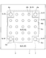
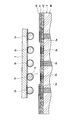
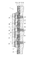
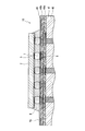
- a semiconductor chip 1 As shown in FIGS. 1 and 2, a semiconductor chip 1 according to an embodiment of the present invention includes a multilayer wiring board 4 and a semiconductor chip 2 mounted on a surface 4 a of the multilayer wiring board 4. .
- the semiconductor chip 2 and an underfill 8 described later are indicated by a two-dot chain line.
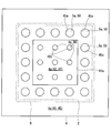
- the semiconductor chip 2 has a flat rectangular plate shape.
- a plurality of (for example, 1000 to 2000, for the sake of simplification, 25 are drawn) electrode pads 3 are provided. These electrode pads 3 may be arranged in a matrix or in a staggered manner.
- Each electrode pad 3 has, for example, a circular shape, and is configured such that a UBM (Under Bump Metal) 32 is laminated on an aluminum pad 31.
- UBM Under Bump Metal
- an electroless nickel plating layer having a thickness of 10 ⁇ m may be formed on the aluminum pad 31, and a gold plating layer having a thickness of 0.1 ⁇ m may be further formed thereon.
- the region other than the electrode pad 3 on the back surface 2a of the semiconductor chip 2 is covered with an insulating protective film 21 made of, for example, polyimide resin.
- the electrode pad 3 is composed of a first electrode pad 3a arranged close to each corner (four vertices) of the back surface 2a of the semiconductor chip 2 and other second electrode pads 3b. Yes.
- the size of the first electrode pad 3a is preferably set larger than the size of the second electrode pad 3b.
- the diameter of the first electrode pad 3a may be 140 ⁇ m
- the diameter of the second electrode pad 3b may be 100 ⁇ m.
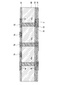
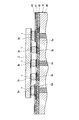
- the multilayer wiring board 4 is an interposer configured by alternately laminating circuit patterns and insulating layers on both the front and back surfaces of the core substrate 40.
- a plurality of connection pads 5 respectively facing the electrode pads 3 are provided on the front surface 4a of the multilayer wiring board 4, and a plurality of external connection pads respectively electrically connected to the connection pads 5 are provided on the back surface 4b. 6 is provided.
- a circuit pattern 51, a second insulating layer (lower insulating layer) 42, a circuit pattern 52, and a first insulating layer (upper insulating layer) 41 are laminated in this order on the surface of the core substrate 40.
- a circuit pattern 61, a third insulating layer 43, a circuit pattern 62, and a fourth insulating layer 44 are laminated in this order.
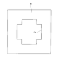
- the first insulating layer 41 has an opening 41 a that exposes the second insulating layer 42 and faces the back surface 2 a of the semiconductor chip 2.
- the connection pad 5 is supported by the first insulating layer 41 and the second insulating layer 42, and the external connection pad 6 is supported by the fourth insulating layer 44.
- the first insulating layer 41 constitutes a first insulating region that supports a first connection pad 5a described later
- the second insulating layer 42 is a second insulating region that supports a second connection pad 5b described later. Is configured.
- the opening 41a is formed in a cross shape. That is, the first insulating layer 41 is formed so as to face only the four corners of the back surface 2a of the semiconductor chip 2 through the opening 41a, and the second insulating layer 42 covers the four corners of the back surface 2a of the semiconductor chip 2 through the opening 41a. Opposite the part.
- Each of the insulating layers 41 to 44 includes the pad 5 (or 6) and the circuit patterns 51 and 52 (or 62) or the circuit patterns 51 and 52 (or 61 and 62) through the insulating layers 41 to 44.
- a via hole 48 is formed for conducting each other.
- the core substrate 40 is provided with a through electrode 40 a that electrically connects the circuit patterns 51 and 61 through the core substrate 40.
- the multilayer wiring board 4 has a front side solder resist 45 that covers the first insulating layer 41 and the second insulating layer 42, and a back side solder resist 46 that covers the fourth insulating layer 44.
- the front surface 4 a of the multilayer wiring board 4 is configured by the outer surface of the front side solder resist 45
- the back surface 4 b of the multilayer wiring substrate 4 is configured by the outer surface of the back side solder resist 46.
- the core substrate 40 a ceramic substrate or an organic material substrate can be used. However, from the viewpoint of effective relaxation of stress applied to the joint portion at the time of cost and thermal stress loading, it is possible to use glass cloth. It is preferable to use a glass epoxy substrate impregnated with a thermosetting resin.
- the thickness of the core substrate 40 is 0.4 mm, for example.
- an epoxy resin is suitable, but other resins can also be used.
- one thermosetting resin having high heat resistance such as bismaleimide triazine resin or thermosetting polyphenylene ether may be used, or a mixture of two or more of these may be used.
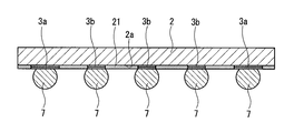
- connection pads 5 are connected to the electrode pads 3 of the semiconductor chip 2 via solder bumps 7, respectively.
- the solder bumps 7 have substantially the same volume (for example, 5.0 ⁇ 10 ⁇ 4 mm 3 ).
- connection pad 5 includes a first connection pad 5a connected to the first electrode pad 3a and a second connection pad 5b connected to the second electrode pad 3b.
- the first connection pad 5 a is supported by the first insulating layer 41
- the second connection pad 5 b is supported by the second insulating layer 42.
- the first connection pads 5a located at the four corners among the plurality of connection pads 5 arranged in the rectangular region on the surface 4a of the multilayer wiring board 4 are supported by the first insulating layer 41, and the remaining second The connection pad 5 b is supported by the second insulating layer 42.
- a height difference equal to the thickness of the first insulating layer 41 is formed between the first connection pad 5a and the second connection pad 5b, and the first connection pad 5a is connected to the second connection by the height difference. It is located closer to the semiconductor chip 2 than the pad 5b.
- the shape of the first connection pad 5a and the second connection pad 5b is not particularly limited, but may be, for example, a circular shape or a rectangular shape.
- the size of the first connection pad 5a is preferably larger than the size of the second connection pad 5b.
- the first connection pad 5a may have a circular shape with a diameter of 140 ⁇ m
- the second connection pad 5b may have a circular shape with a diameter of 100 ⁇ m.
- the first insulating layer 41 is preferably made of a thermoplastic resin.
- the thermoplastic resin constituting the first insulating layer 41 is not particularly limited, but from the viewpoint of the manufacturing method, adhesion, and workability of the multilayer wiring board, for example, polyphenylene ether (PPE), liquid crystal polymer (LCP) ), Polyetheretherketone (PEEK), polyetherimide (PEI), polyethersulfone (PES), thermoplastic polyimide (PI), etc. Can do.
- the thermoplastic resin constituting the first insulating layer 41 has a melting point of 280 ° C. or higher.
- a temperature for example, 260 ° C.
- the melting point of the solder bump 7 for example, 217 ° C. for a solder bump having a composition of 97.5 wt% tin and 2.5 wt% silver
- the thickness of the first insulating layer 41 is preferably 1.5 times or more the thickness of the circuit pattern 52 immediately below the first insulating layer 41 in the multilayer wiring board. Since the circuit pattern 52 is formed so as to be embedded in the first insulating layer 41, the circuit pattern cannot be formed above and below the first insulating layer 41 if the first insulating layer 41 is thinner than the circuit pattern 52. Further, if the thickness of the first insulating layer 41 is less than 1.5 times the thickness of the circuit pattern 52, the first insulating layer 41 may be processed by etching or the like when forming the circuit pattern, or by surface roughening when forming the insulating layer.
- the thickness of the first insulating layer 41 is preferably less than or equal to one half of the height of the solder bump 7 formed between the second electrode pad 3b and the second connection pad 5b.
- the thickness of the first insulating layer 41 exceeds one half of the height of the solder bump 7 formed between the second electrode pad 3b and the second connection pad 5b, the first connection pad 5a and the second connection are connected. This is because the height difference between the pads 5b becomes too large, and the solder bumps 7 connected to the first connection pads 5a are extremely crushed, which may reduce the connection reliability.
- the thickness of the first insulating layer 41 may be 5 to 50 ⁇ m.
- the second to fourth insulating layers 42 to 44 are preferably made of a thermosetting resin containing an inorganic filler.
- the inorganic filler is added in order to lower the thermal expansion coefficient and improve the elastic modulus while maintaining the insulating properties of the insulating layer, and its blending amount is, for example, 10 to 60% by volume.
- the inorganic filler include spherical silica having an average particle diameter of 5 ⁇ m. In addition to silica, spherical or crushed fillers made of alumina, aluminum hydroxide, barium titanate or the like may be used.
- thermosetting resin an epoxy resin is suitable, but other resins can be used.
- one thermosetting resin having high heat resistance such as bismaleimide triazine resin or thermosetting polyphenylene ether may be used, or a mixture of two or more of these may be used.
- the front side solder resist 45 is provided with openings 45a and 45b (see FIG. 2) for exposing the first connection pad 5a and the second connection pad 5b at positions corresponding to the first connection pad 5a and the second connection pad 5b. ing.
- the size of the opening 45a at the position corresponding to the first connection pad 5a is preferably set larger than the size of the opening 45b at the position corresponding to the second connection pad 5b.
- the size of the opening 45a may be 130 ⁇ m in diameter, and the size of the opening 45b may be 90 ⁇ m in diameter.
- the size of the opening 45a at the position corresponding to the first connection pad 5a may be determined according to the thickness of the first insulating layer 41 and the volume of the solder bump 7.
- the thickness of the front side solder resist layer 45 is, for example, 20 ⁇ m.
- a barrier metal layer 50 is laminated on the first connection pad 5a and the second connection pad 5b exposed through the openings 45a and 45b.
- an electroless nickel plating layer having a thickness of 10 ⁇ m is formed on the first connection pad 5a and the second connection pad 5b, and further a gold having a thickness of 0.1 ⁇ m is formed thereon.
- a plating layer may be formed.
- the first connection pad 5 a and the second connection pad 5 b are connected to the solder bump 7 via the barrier metal layer 50.
- An opening is also formed in the back side solder resist 46 at a position corresponding to the external connection pad 6, and a barrier metal layer 60 is formed in the opening.
- an underfill 8 is filled between the multilayer wiring board 4 and the semiconductor chip 2.
- a polyfunctional epoxy resin is often used from the viewpoint of heat resistance, and in particular, an insulating resin such as a bisphenol A novolac epoxy resin, a bisphenol F novolac epoxy resin, or a cresol novolac epoxy resin. Can be used.
- the solder bumps 7 positioned at the four corners that are most stressed when the semiconductor chip 2 and the multilayer wiring board 4 are connected via the solder bumps 7 are the first insulating layer made of thermoplastic resin.
- the first connection pads 5 a formed on the first connection pads 5 a are connected.
- the stress applied to the solder bumps 7 positioned at the four corners can be alleviated.
- solder bumps 7 are connected to the second connection pads 5b formed on the second insulating layer 42 having a high elastic modulus even during a thermal load, the semiconductor chip 2 and the multilayer wiring board 4 As a whole, the connection can be made rigid and strong. Furthermore, since the cross-sectional area of the solder bump 7 located at the four corners can be greatly expanded by the height difference between the first connection pad 5a and the second connection pad 5b, the stress applied to the solder bump 7 is further reduced. be able to. Therefore, even if the solder bumps 7 having substantially the same volume are used as in this embodiment, the generation of cracks can be effectively suppressed and the bonding strength between the semiconductor chip 2 and the multilayer wiring board 4 is high. A semiconductor device can be obtained.
- solder bumps 7 having substantially the same volume are used as in the present embodiment, the solder bumps 7 can be formed by the ball mounting method, so that even if the connection pad pitch is as narrow as 200 ⁇ m or less, solder is used. The bump 7 can be formed satisfactorily.
- FIG. 3 is a cross-sectional view showing a state before the first insulating layer 41 is formed.
- a metal foil having a thickness of 15 ⁇ m is bonded to both the front and back surfaces of the core substrate 40 by thermocompression bonding.
- a copper foil produced by electrolytic plating can be used.
- a carbon dioxide laser is used to process a through hole that penetrates the core substrate 40 together with the metal foil, and then the inside of the through hole is electroless copper plated.
- the through electrode 40a is formed by filling with electrolytic copper plating.
- the circuit patterns 51 and 61 are formed on the core substrate 40 by etching the metal foil.
- thermosetting resin containing an inorganic filler as described above is bonded to the surface of the core substrate 40 on which the circuit pattern 51 is formed by thermocompression bonding and cured, and the first Two insulating layers 42 are formed.
- the method for forming the second insulating layer 42 is not limited to this.
- an uncured liquid thermosetting resin containing an inorganic filler is applied by screen printing or spin coating, and then heated and cured. Also good.
- a bottomed via hole 48 that penetrates the second insulating layer 42 in the thickness direction and reaches the circuit pattern 51 therebelow is formed in the second insulating layer 42 using a carbon dioxide laser.
- the bottomed via hole 48 may be formed by using a laser processing apparatus such as a third harmonic Nd-YAG laser or a deep ultraviolet excimer laser having a wavelength shorter than 300 nm, in addition to the carbon dioxide gas laser.
- a photosensitive dry film resist is bonded to the surface of the formed copper plating film by a thermocompression press, and a glass mask on which a negative image of a desired conductor pattern is drawn is positioned thereon. Thereafter, exposure and development are performed to form an etching resist that exposes the copper plating film in portions other than the necessary conductor pattern.
- the portion of the copper plating film not covered with the etching resist was dissolved and removed by etching, and then the etching resist was peeled off to be electrically connected to the circuit pattern 51 on the second insulating layer 42.
- a second connection pad 5b and a circuit pattern 52 are formed.
- the third insulating layer 43, the circuit pattern 62 electrically connected to the circuit pattern 61, the fourth insulating layer 44, and the circuit pattern 62 are electrically connected to the back surface of the core substrate 40 in the same manner as described above. External connection pads 6 connected to are formed.
- the opening 41 a made of the thermoplastic resin as described above is formed to cover all portions other than the region where the second connection pad 5 b on the second insulating layer 42 is disposed.
- a film 41 ′ having a shape capable of being prepared is prepared.
- the opening 41a may be formed by cutting out the film with a carbon dioxide laser, for example.
- the first insulating layer 41 is formed so as to surround the second connection pad 5 b by thermocompression bonding after positioning the film 41 ′ on the second insulating layer 42.
- the formation of the first insulating layer 41 can be performed by applying a liquid thermoplastic resin onto the second insulating layer 42. However, considering the ease and cost of the multilayer wiring board manufacturing method, the film 41 ′ is formed. Is preferably used.
- the first connection pad 5 a is formed on the first insulating layer 41 by the same method as the method of forming the second connection pad 5 b on the second insulating layer 42.
- a solder resist resin made of a photosensitive epoxy resin is used on the first insulating layer 41 and the second insulating layer 42 by an exposure process. Then, a front-side solder resist 45 having openings 45a and 45b exposing the first connection pad 5a and the second connection pad 5b is formed. Since there is a step between the first insulating layer 41 and the second insulating layer 42 that form the foundation for forming the front side solder resist 45, when forming the front side solder resist 45, first, a portion on the second insulating layer 42 is formed. Is formed first, and then a portion on the first insulating layer 41 is formed.
- a back side solder resist 46 having an opening exposing the external connection pad 6 is formed on the fourth insulating layer 44. Since the back side has no step on the base, the back side solder resist 46 can be formed by a single process after the front side solder resist 45 is formed.
- the formation of these solder resists 45 and 46 is generally performed by using a photosensitive type solder resist material and patterning by an exposure process, but any method can be used as long as it can be processed into a desired shape. Also good. For example, processing may be performed using a laser processing apparatus such as a carbon dioxide laser, a third harmonic Nd-YAG laser, or a deep ultraviolet excimer laser having a wavelength shorter than 300 nm.
- barrier metal layers 50 and 60 are formed on portions of the first connection pad portion 5a, the second connection pad 5b, and the external connection pad 6 exposed from the openings of the solder resists 45 and 46, respectively.
- a multilayer wiring board 4 as shown in FIG. 5 can be manufactured.
- solder balls having a diameter of 100 ⁇ m are mounted at predetermined positions on the first electrode pad 3a and the second electrode pad 3b of the semiconductor chip 2, and reflow treatment is performed in a nitrogen gas atmosphere. By doing so, the solder bumps 7 are formed.
- flax 71 is attached to the solder bumps 7.
- the method of attaching the flux 71 to the solder bumps 7 is particularly effective when the flux 71 is spread over the entire surface of the solder bumps 7 and the flux 71 does not adhere to the insulating protective film 21 formed on the back surface 2a of the semiconductor chip 2. It doesn't matter.
- the solder bumps 7 formed on the semiconductor chip 2 are immersed in a flux 71 uniformly applied to a flat surface with a film thickness (for example, 50 ⁇ m) thinner than the height of the solder bumps 7.
- the flux 71 can be adhered.
- the wettability of the flux 71 with respect to the solder causes the flux 71 to wet out to the portion of the solder bump 7 that is not immersed in the flux 71, and the surface of the solder bump 7 is uniformly covered with the flux 71. Can do.
- the multilayer wiring board 4 and the semiconductor chip 2 are aligned so as to have a predetermined positional relationship, and the semiconductor is mounted on the surface 4a of the multilayer wiring board 4.
- the chip 2 is mounted so that the connection pads 5 and the electrode pads 3 face each other with the solder bumps 7 interposed therebetween.
- the solder bumps 7 are only in contact with the first connection pads 5a and the second connection pads 5b of the multilayer wiring board 4 via the flux 71 (more precisely, also through the barrier metal layer 50). Yes, no solder connection is made.
- the multilayer wiring board 4 on which the semiconductor chip 2 is mounted is heated for 20 seconds or more at a temperature 30 ° C. higher than the temperature at which the solder bumps 7 are melted in a nitrogen atmosphere (reflow treatment is performed). 8), the semiconductor chip 2 is mounted on the surface 4a of the multilayer wiring board 4 by the solder bumps 7, as shown in FIG.
- the flux 71 is washed.
- the mounting body in which the semiconductor chip 2 is mounted on the multilayer wiring board 4 as shown in FIG. 8 is completely immersed in the cleaning liquid, and cleaning with ultrasonic waves having a frequency of 100 kHz and an output of 100 W is performed for 5 minutes.
- the mounting body taken out from the cleaning liquid is immediately rinsed with pure water for 5 minutes.
- the cleaning liquid effectively enters the gap portion where the solder bumps 7 of the mounting body are present, and the residual flux is removed relatively efficiently. be able to.
- the semiconductor chip of the dummy sample was peeled off after mounting and the periphery of the solder bump 7 was observed, there was no residual flux around the solder bump 7.
- the ultrasonic power In order to enhance the cleaning effect, it is preferable to increase the ultrasonic power during cleaning. However, if the ultrasonic power is higher than 1000 W, cracks are generated in the solder bumps 7 or the electrode pads 3, and if the ultrasonic power is lower than 50 W, the residue is increased. The flux is not removed at all. Therefore, the ultrasonic output is preferably 50 W or more and 1000 W or less. Further, when the ultrasonic frequency is higher than 600 kHz and lower than 50 kHz, the residual flux is not removed, and therefore the ultrasonic frequency is preferably 50 kHz or more and 600 kHz or less.
- the cleaning time and the rinsing time are longer than 1 minute, there is no difference in the removability of the remaining flux, but the long-time ultrasonic treatment absorbs moisture in the multilayer wiring board 4, and the subsequent heat treatment process Therefore, it is preferable that the time is 10 minutes or less because there is a risk of causing swelling or delamination in the multilayer wiring board 4.
- the mounting body as shown in FIG. 8 after the flux cleaning is completed is baked for 1 hour at 115 to 125 ° C. in a nitrogen atmosphere.
- the baking time is shorter than 1 hour, or when the baking temperature is lower than 115 ° C., the surface adsorbed water adhering to the surface 4a of the multilayer wiring board 4 is not sufficiently removed, and in the next underfill filling step.
- the wettability of the underfill 8 with respect to the surfaces of the solder resists 45 and 46 is lowered, and the underfill 8 is not sufficiently filled.
- the baking time exceeds 3 hours, or when the baking temperature exceeds 125 ° C., the surfaces of the solder resists 45 and 46 are discolored. Therefore, the baking time is preferably 1 hour or more and 3 hours or less, and the baking temperature is preferably 115 ° C. or more and 125 ° C. or less.
- the uncured underfill 8 is applied to the gap portion between the multilayer wiring board 4 and the semiconductor chip 2 by an underfill coating apparatus.
- the underfill 8 is applied in a predetermined amount along the longest side among the four sides forming the outer shape of the semiconductor chip 2.
- the underfill 8 is applied to the multilayer wiring board 4 on which the semiconductor chip 2 as shown in FIG. 8 is mounted in order to lower the viscosity of the applied underfill 8 and increase the permeability to the gap portion (gap). Is preferably performed in a state of being heated to 65 ° C., for example. Even after the application, for example, by maintaining the same temperature for about 10 minutes, the underfill 8 can be completely filled in the gap portion by utilizing the permeability of the underfill 8.
- the mounting body filled with the underfill 8 between the multilayer wiring board 4 and the semiconductor chip 2 is put into an oven and heated at a temperature of, for example, 145 to 155 ° C. for 1 hour in a nitrogen atmosphere.
- a temperature of, for example, 145 to 155 ° C. for 1 hour in a nitrogen atmosphere.
- the uncured underfill 8 is cured, so that the solder bumps 7 are sealed and joined from moisture intrusion and external stress, as well as compression and shear stress generated by thermal deformation and internal residual stress.
- the role is to protect the department.
- the heating temperature is lower than 130 ° C. or when the heating time is shorter than 1 hour, the underfill 8 is not sufficiently cured, and the electrical insulation is deteriorated due to the ingress of moisture, or the sealing effect is not good.
- the joint will break.
- the heating temperature exceeds 170 ° C. or when the heating time exceeds 3 hours, the multilayer wiring board 4 is deformed by the excessive curing reaction of the underfill 8, or the joint portion or the multilayer wiring board is formed. 4 breakage or peeling occurs.
- the semiconductor device 1 as shown in FIG. 1 can be manufactured.
- solder bumps 7 are formed on the electrode pads 3 of the semiconductor chip 2, but the solder is applied to both the electrode pads 3 of the semiconductor chip 2 and the connection pads 5 of the multilayer wiring board 4. Bumps may be formed and the solder bumps 7 may be formed by joining the solder bumps.
- the 1st insulating layer 41 was comprised with the thermoplastic resin, the 1st insulating layer 41 may be comprised with the thermosetting resin same as the 2nd insulating layer 42.
- the solder bump 7 connected to the first connection pad 5a is more than the solder bump 7 connected to the second connection pad 5b due to the difference in height between the first connection pad 5a and the second connection pad 5b.
- the shape can be expanded, and the generation of cracks due to thermal stress can be suppressed.
- the 1st insulating layer 41 does not need to be laminated
- the 1st insulating layer 41 and the 2nd insulating layer 42 may be laminated
- the first insulating layer 41 is made of a thermoplastic resin and the first insulating layer 41 is laminated on the second insulating layer 42 as in the above embodiment, due to the synergistic effect thereof, The generation of cracks can be more effectively suppressed.
- angular of the back surface 2a of the semiconductor chip 2 among the electrode pads 3 becomes the 1st electrode pad 3a, and the remaining electrode pads become the 2nd electrode pad 3b.
- the first electrode pad 3a only needs to include at least the electrode pad 3a disposed in the vicinity of each corner of the back surface 2a of the semiconductor chip 2.
- the connection pads located at least at the four corners of the connection pads 5 may be supported by the first insulating layer 41.
- all the electrode pads on the outermost periphery of the electrode pads 3 may be the first electrode pads 3a, and the electrode pads surrounded by the first electrode pads 3a may be the second electrode pads 3b. That is, as shown in FIG.
- all of the outermost connection pads of the connection pads 5 may be the first connection pads 5 a and supported by the first insulating layer 41.
- the shape and size of the opening 41a formed in the first insulating layer 41 can be appropriately changed in accordance with the arrangement of the first connection pads 5a connected to the first electrode pads 3a via the solder bumps 7. It is.
- the present invention is also applicable when a wafer level CSP is mounted on a mounting board. That is, the multilayer wiring board 4 does not have to be an interposer, and may be a two-layer or three-layer board in which the first insulating layer 41 and the second insulating layer 42 are formed only on the surface of the core substrate 40, for example. .
- the present invention can provide the same effect even when, for example, gold bumps other than solder bumps are used as bumps.
- the semiconductor device is pretreated for moisture storage under conditions specified by JEDEC STANDARD TEST METHOD A113-A LEVEL3, and immediately after that, a solder reflow test is performed three times at a temperature of 260 ° C. Went.
- a cycle in which the semiconductor device thus pretreated is placed in an environment of ⁇ 55 ° C. for 30 minutes and then placed in an environment of 125 ° C. for 30 minutes is performed 1000 cycles and 1500 cycles. The change of the connection resistance value of the wiring part was confirmed.
- Example 1 In Example 1, a semiconductor chip 2 having a size of 8.0 ⁇ 8.0 mm was used, and the number of electrode pads 3, connection pads 5, and solder bumps 7 was 1600 (pad pitch: 180 ⁇ m). A glass epoxy substrate was used as the core substrate 40. Polyphenylene ether is used as the thermoplastic resin constituting the first insulating layer 41, and 50% by volume of spherical silica (inorganic filler) having an average particle diameter of 5 ⁇ m is blended as the thermosetting resin constituting the second insulating layer. Epoxy resin was used. The thickness of the first insulating layer 41 existing on the outermost surface was 30 ⁇ m, and the thickness of the second insulating layer 42 was 45 ⁇ m. Others (the volume of the solder bump 7, the shape and size of the electrode pad 3 and the connection pad 5, the size of the openings 45a and 45b, etc.) are those specifically exemplified in the above embodiment. A semiconductor device was manufactured under the above conditions.
- the change rate of the connection resistance value after 1000 cycles which is the criterion for reliability evaluation, is + 10% or less with respect to the initial resistance value, and after 1500 cycles.
- the change rate of the connection resistance value was also + 10% or less with respect to the initial resistance value, and it was found that the connection resistance value had good resistance to repeated temperature changes.
- Example 2 Compared to Example 1, the size of the opening 45a at the position corresponding to the first connection pad 5a in the front-side solder resist 45 was changed from 130 ⁇ m to 90 ⁇ m, which is the same as the other opening 45b, under the same conditions as in Example 1. A semiconductor device was manufactured.
- the change rate of the connection resistance value after 1000 cycles was + 10% or less with respect to the initial resistance value.
- a partial disconnection failure occurred after 1500 cycles.
- it corresponds to the upper part of the opening 45a of the front solder resist 45a in the solder bump 7 related to the generated disconnection location. Cracks starting from the position were observed.
- Example 3 Compared to Example 1, the thickness of the first insulating layer 41 is changed to 45 ⁇ m so that the thickness of the solder bump 7 formed between the second electrode pad 3b and the second connection pad 5b is 1 ⁇ 2.
- a semiconductor device was manufactured under the same conditions as in Example 1 except that.
- the change rate of the connection resistance value after 1000 cycles was + 10% or less with respect to the initial resistance value.
- a partial disconnection failure occurred.
- the solder bump 7 related to the generated disconnection portion is greatly crushed and deformed as compared with the first embodiment. Cracks were observed in the solder bumps along the deformed portion.
- the multilayer wiring board 4 ′ according to the comparative example has a structure in which the connection pads 5 connected to the electrode pads 3 of the semiconductor chip 2 via the solder bumps 7 are all formed on the same insulating layer.
- the multilayer wiring board 4 ′ according to this comparative example is manufactured in the same manner as in the above embodiment until the insulating layer 49a corresponding to the second insulating layer is formed, and the insulating layer 49b is formed on the entire surface of the insulating layer 49a. It was formed of the same material as 49a (thermosetting resin containing an inorganic filler).
- the change rate of the connection resistance value exceeds + 10% with respect to the initial resistance value after 200 cycles, the disconnection failure occurs after 500 cycles, and the resistance to the temperature change is inferior. It was confirmed.
- the present invention is particularly useful when the size of a semiconductor chip is relatively large and when the volume of individual solder bumps is small.
Landscapes
- Engineering & Computer Science (AREA)
- Microelectronics & Electronic Packaging (AREA)
- Physics & Mathematics (AREA)
- Computer Hardware Design (AREA)
- Power Engineering (AREA)
- Condensed Matter Physics & Semiconductors (AREA)
- General Physics & Mathematics (AREA)
- Manufacturing & Machinery (AREA)
- Geometry (AREA)
- Production Of Multi-Layered Print Wiring Board (AREA)
- Electric Connection Of Electric Components To Printed Circuits (AREA)
- Wire Bonding (AREA)
Priority Applications (1)
| Application Number | Priority Date | Filing Date | Title |
|---|---|---|---|
| US12/707,927 US8324740B2 (en) | 2008-03-25 | 2010-02-18 | Semiconductor device, and method of manufacturing multilayer wiring board and semiconductor device |
Applications Claiming Priority (4)
| Application Number | Priority Date | Filing Date | Title |
|---|---|---|---|
| JP2008-077557 | 2008-03-25 | ||
| JP2008077557 | 2008-03-25 | ||
| JP2009001253A JP5150518B2 (ja) | 2008-03-25 | 2009-01-07 | 半導体装置および多層配線基板ならびにそれらの製造方法 |
| JP2009-001253 | 2009-01-07 |
Related Child Applications (1)
| Application Number | Title | Priority Date | Filing Date |
|---|---|---|---|
| US12/707,927 Continuation US8324740B2 (en) | 2008-03-25 | 2010-02-18 | Semiconductor device, and method of manufacturing multilayer wiring board and semiconductor device |
Publications (1)
| Publication Number | Publication Date |
|---|---|
| WO2009118999A1 true WO2009118999A1 (ja) | 2009-10-01 |
Family
ID=41113216
Family Applications (1)
| Application Number | Title | Priority Date | Filing Date |
|---|---|---|---|
| PCT/JP2009/000719 Ceased WO2009118999A1 (ja) | 2008-03-25 | 2009-02-19 | 半導体装置ならびに多層配線基板および半導体装置の製造方法 |
Country Status (3)
| Country | Link |
|---|---|
| US (1) | US8324740B2 (enExample) |
| JP (1) | JP5150518B2 (enExample) |
| WO (1) | WO2009118999A1 (enExample) |
Cited By (3)
| Publication number | Priority date | Publication date | Assignee | Title |
|---|---|---|---|---|
| CN102209434A (zh) * | 2010-03-30 | 2011-10-05 | 富士通株式会社 | 印制电路板以及印制电路板的制造方法 |
| US20110285016A1 (en) * | 2010-05-20 | 2011-11-24 | Panasonic Corporation | Semiconductor device and method of manufacturing the same |
| JPWO2016114358A1 (ja) * | 2015-01-16 | 2017-08-17 | 株式会社村田製作所 | 基板、基板の製造方法及び弾性波装置 |
Families Citing this family (42)
| Publication number | Priority date | Publication date | Assignee | Title |
|---|---|---|---|---|
| JP2010161136A (ja) * | 2009-01-07 | 2010-07-22 | Panasonic Corp | 半導体装置及びその製造方法 |
| JP5263053B2 (ja) * | 2009-07-24 | 2013-08-14 | 株式会社村田製作所 | 半導体パッケージおよび半導体パッケージモジュール |
| JP5357784B2 (ja) * | 2010-01-05 | 2013-12-04 | パナソニック株式会社 | 半導体装置及びその製造方法 |
| US20120032337A1 (en) * | 2010-08-06 | 2012-02-09 | Taiwan Semiconductor Manufacturing Company, Ltd. | Flip Chip Substrate Package Assembly and Process for Making Same |
| JP5644286B2 (ja) * | 2010-09-07 | 2014-12-24 | オムロン株式会社 | 電子部品の表面実装方法及び電子部品が実装された基板 |
| US8624392B2 (en) | 2011-06-03 | 2014-01-07 | Taiwan Semiconductor Manufacturing Company, Ltd. | Electrical connection for chip scale packaging |
| US8674235B2 (en) * | 2011-06-06 | 2014-03-18 | Intel Corporation | Microelectronic substrate for alternate package functionality |
| US20130244382A1 (en) * | 2011-09-15 | 2013-09-19 | Flipchip International, Llc | High precision self aligning die for embedded die packaging |
| US8912668B2 (en) | 2012-03-01 | 2014-12-16 | Taiwan Semiconductor Manufacturing Company, Ltd. | Electrical connections for chip scale packaging |
| US9548281B2 (en) | 2011-10-07 | 2017-01-17 | Taiwan Semiconductor Manufacturing Company, Ltd. | Electrical connection for chip scale packaging |
| KR20130057314A (ko) * | 2011-11-23 | 2013-05-31 | 삼성전기주식회사 | 인쇄회로기판 및 인쇄회로기판 제조 방법 |
| KR101921258B1 (ko) | 2012-05-09 | 2018-11-22 | 삼성전자주식회사 | 배선 기판 및 이를 포함하는 반도체 패키지 |
| US9196573B2 (en) | 2012-07-31 | 2015-11-24 | Taiwan Semiconductor Manufacturing Company, Ltd. | Bump on pad (BOP) bonding structure |
| US9673161B2 (en) | 2012-08-17 | 2017-06-06 | Taiwan Semiconductor Manufacturing Company, Ltd. | Bonded structures for package and substrate |
| US8829673B2 (en) | 2012-08-17 | 2014-09-09 | Taiwan Semiconductor Manufacturing Company, Ltd. | Bonded structures for package and substrate |
| JP2014082281A (ja) * | 2012-10-15 | 2014-05-08 | Olympus Corp | 基板、半導体装置、基板の製造方法 |
| US9147663B2 (en) | 2013-05-28 | 2015-09-29 | Intel Corporation | Bridge interconnection with layered interconnect structures |
| JP5959562B2 (ja) * | 2013-05-30 | 2016-08-02 | 京セラ株式会社 | 配線基板 |
| JP5997200B2 (ja) * | 2013-05-30 | 2016-09-28 | 京セラ株式会社 | 配線基板 |
| JP5997197B2 (ja) * | 2013-05-30 | 2016-09-28 | 京セラ株式会社 | 配線基板 |
| JP6096640B2 (ja) * | 2013-06-28 | 2017-03-15 | 京セラ株式会社 | 配線基板 |
| JP6316609B2 (ja) * | 2014-02-05 | 2018-04-25 | 新光電気工業株式会社 | 配線基板及び半導体装置と配線基板の製造方法及び半導体装置の製造方法 |
| WO2015129600A1 (ja) * | 2014-02-26 | 2015-09-03 | 株式会社村田製作所 | 多層基板の製造方法、及び多層基板 |
| KR101630769B1 (ko) * | 2014-06-24 | 2016-06-16 | 매그나칩 반도체 유한회사 | 방열 반도체 칩 패키지 및 그 제조 방법 |
| JP5795415B1 (ja) * | 2014-08-29 | 2015-10-14 | 新光電気工業株式会社 | 配線基板及びその製造方法 |
| JP6515724B2 (ja) * | 2015-07-31 | 2019-05-22 | 富士通株式会社 | 半導体装置 |
| US10074624B2 (en) * | 2015-08-07 | 2018-09-11 | Analog Devices, Inc. | Bond pads with differently sized openings |
| JP6502205B2 (ja) * | 2015-08-07 | 2019-04-17 | 日本特殊陶業株式会社 | 多層配線基板およびその製造方法 |
| US10692813B2 (en) * | 2016-11-28 | 2020-06-23 | Taiwan Semiconductor Manufacturing Co., Ltd. | Semiconductor package with dummy bumps connected to non-solder mask defined pads |
| MY192082A (en) * | 2016-12-27 | 2022-07-26 | Intel Corp | Interconnect core |
| CN107068845B (zh) * | 2017-05-19 | 2024-03-19 | 深圳大道半导体有限公司 | 组合式半导体结构及灯具 |
| CN109803481B (zh) * | 2017-11-17 | 2021-07-06 | 英业达科技有限公司 | 多层印刷电路板及制作多层印刷电路板的方法 |
| JP7133329B2 (ja) * | 2018-03-23 | 2022-09-08 | 京セラ株式会社 | 配線基板 |
| US10813228B2 (en) | 2018-06-22 | 2020-10-20 | Indium Corporation | Preventing post reflow interconnect failures in VIPPO solder joints via utilization of adhesive material |
| WO2020047519A1 (en) * | 2018-08-31 | 2020-03-05 | Skyworks Solutions, Inc. | Devices and methods related to nested filters |
| JP7283909B2 (ja) * | 2019-01-30 | 2023-05-30 | 京セラ株式会社 | 配線基板および実装構造 |
| JP7290960B2 (ja) * | 2019-03-11 | 2023-06-14 | ローム株式会社 | 半導体装置 |
| TWI701979B (zh) * | 2019-05-17 | 2020-08-11 | 欣興電子股份有限公司 | 線路板及其製作方法 |
| KR102599631B1 (ko) | 2020-06-08 | 2023-11-06 | 삼성전자주식회사 | 반도체 칩, 반도체 장치, 및 이를 포함하는 반도체 패키지 |
| JP7102481B2 (ja) * | 2020-10-09 | 2022-07-19 | Nissha株式会社 | 射出成形品及びその製造方法 |
| JP7716875B2 (ja) * | 2021-04-08 | 2025-08-01 | 上海天馬微電子有限公司 | 積層基板、半導体パッケージ及び半導体パッケージの製造方法 |
| US20230307336A1 (en) * | 2022-03-25 | 2023-09-28 | Qualcomm Incorporated | Package substrates employing pad metallization layer for increased signal routing capacity, and related integrated circuit (ic) packages and fabrication methods |
Citations (2)
| Publication number | Priority date | Publication date | Assignee | Title |
|---|---|---|---|---|
| JPH0964095A (ja) * | 1995-08-24 | 1997-03-07 | Matsushita Electric Ind Co Ltd | バンプ付ワークおよびその実装方法 |
| WO2005034231A1 (ja) * | 2003-10-06 | 2005-04-14 | Nec Corporation | 電子デバイスおよびその製造方法 |
Family Cites Families (10)
| Publication number | Priority date | Publication date | Assignee | Title |
|---|---|---|---|---|
| JPH06204288A (ja) | 1992-03-18 | 1994-07-22 | Nec Corp | 半導体装置 |
| JP3961092B2 (ja) * | 1997-06-03 | 2007-08-15 | 株式会社東芝 | 複合配線基板、フレキシブル基板、半導体装置、および複合配線基板の製造方法 |
| EP2265101B1 (en) * | 1999-09-02 | 2012-08-29 | Ibiden Co., Ltd. | Printed circuit board and method of manufacturing printed circuit board |
| JP3374812B2 (ja) | 1999-11-10 | 2003-02-10 | 日本電気株式会社 | 半導体装置 |
| US7129158B2 (en) * | 2001-09-28 | 2006-10-31 | Ibiden Co., Ltd. | Printed wiring board and production method for printed wiring board |
| JP2007096198A (ja) | 2005-09-30 | 2007-04-12 | Fujikura Ltd | 半導体装置及びその製造方法並びに電子装置 |
| JP2007165420A (ja) * | 2005-12-12 | 2007-06-28 | Matsushita Electric Ind Co Ltd | 半導体装置 |
| JP2007242782A (ja) | 2006-03-07 | 2007-09-20 | Fujikura Ltd | 半導体装置及び電子装置 |
| TWI325745B (en) * | 2006-11-13 | 2010-06-01 | Unimicron Technology Corp | Circuit board structure and fabrication method thereof |
| US7750459B2 (en) * | 2008-02-01 | 2010-07-06 | International Business Machines Corporation | Integrated module for data processing system |
-
2009
- 2009-01-07 JP JP2009001253A patent/JP5150518B2/ja not_active Expired - Fee Related
- 2009-02-19 WO PCT/JP2009/000719 patent/WO2009118999A1/ja not_active Ceased
-
2010
- 2010-02-18 US US12/707,927 patent/US8324740B2/en active Active
Patent Citations (2)
| Publication number | Priority date | Publication date | Assignee | Title |
|---|---|---|---|---|
| JPH0964095A (ja) * | 1995-08-24 | 1997-03-07 | Matsushita Electric Ind Co Ltd | バンプ付ワークおよびその実装方法 |
| WO2005034231A1 (ja) * | 2003-10-06 | 2005-04-14 | Nec Corporation | 電子デバイスおよびその製造方法 |
Cited By (5)
| Publication number | Priority date | Publication date | Assignee | Title |
|---|---|---|---|---|
| CN102209434A (zh) * | 2010-03-30 | 2011-10-05 | 富士通株式会社 | 印制电路板以及印制电路板的制造方法 |
| EP2373135A1 (en) * | 2010-03-30 | 2011-10-05 | Fujitsu Limited | Printed Circuit Board and Method of Fabricating Printed Circuit Board |
| CN102209434B (zh) * | 2010-03-30 | 2013-10-30 | 富士通株式会社 | 印制电路板以及印制电路板的制造方法 |
| US20110285016A1 (en) * | 2010-05-20 | 2011-11-24 | Panasonic Corporation | Semiconductor device and method of manufacturing the same |
| JPWO2016114358A1 (ja) * | 2015-01-16 | 2017-08-17 | 株式会社村田製作所 | 基板、基板の製造方法及び弾性波装置 |
Also Published As
| Publication number | Publication date |
|---|---|
| JP5150518B2 (ja) | 2013-02-20 |
| JP2009260255A (ja) | 2009-11-05 |
| US8324740B2 (en) | 2012-12-04 |
| US20100140800A1 (en) | 2010-06-10 |
Similar Documents
| Publication | Publication Date | Title |
|---|---|---|
| JP5150518B2 (ja) | 半導体装置および多層配線基板ならびにそれらの製造方法 | |
| US8513818B2 (en) | Semiconductor device and method for fabricating the same | |
| JP4361826B2 (ja) | 半導体装置 | |
| KR100232414B1 (ko) | 다층회로기판 및 그 제조방법 | |
| JP5711472B2 (ja) | 配線基板及びその製造方法並びに半導体装置 | |
| JP3891838B2 (ja) | 半導体装置およびその製造方法 | |
| KR101027711B1 (ko) | 다층 배선 기판의 제조 방법 | |
| JP2004335641A (ja) | 半導体素子内蔵基板の製造方法 | |
| US8450848B2 (en) | Semiconductor device and method for fabricating the same | |
| US9338886B2 (en) | Substrate for mounting semiconductor, semiconductor device and method for manufacturing semiconductor device | |
| TW200938020A (en) | Part built-in wiring board, and manufacturing method for the part built-in wiring board | |
| WO2020090601A1 (ja) | 半導体パッケージ用配線基板及び半導体パッケージ用配線基板の製造方法 | |
| JP2020004926A (ja) | 配線基板及び配線基板の製造方法 | |
| JP2000174050A (ja) | 半導体チップ及び半導体チップの製造方法 | |
| JP2021158200A (ja) | 半導体装置、及び半導体装置の製造方法 | |
| JP7196936B2 (ja) | 半導体装置用配線基板の製造方法、及び半導体装置用配線基板 | |
| JP5509295B2 (ja) | 半導体装置 | |
| JP4324732B2 (ja) | 半導体装置の製造方法 | |
| JP2011146490A (ja) | 回路基板及びその製造方法、半導体装置、並びに電子回路装置 | |
| JP2002064162A (ja) | 半導体チップ | |
| JP2003229451A (ja) | フリップチップ実装構造 | |
| JP7087369B2 (ja) | 微細配線層付きキャリア基板および微細配線層付き半導体パッケージ基板の製造方法 | |
| JP4593444B2 (ja) | 電子部品実装構造体の製造方法 | |
| JP2021097104A (ja) | 複合配線基板及び複合配線基板の製造方法 | |
| JP2003037210A (ja) | 半導体装置およびその製造方法 |
Legal Events
| Date | Code | Title | Description |
|---|---|---|---|
| 121 | Ep: the epo has been informed by wipo that ep was designated in this application |
Ref document number: 09724265 Country of ref document: EP Kind code of ref document: A1 |
|
| NENP | Non-entry into the national phase |
Ref country code: DE |
|
| 122 | Ep: pct application non-entry in european phase |
Ref document number: 09724265 Country of ref document: EP Kind code of ref document: A1 |