US9493348B2 - Nanoparticulate encapsulation barrier stack - Google Patents
Nanoparticulate encapsulation barrier stack Download PDFInfo
- Publication number
- US9493348B2 US9493348B2 US12/513,569 US51356909A US9493348B2 US 9493348 B2 US9493348 B2 US 9493348B2 US 51356909 A US51356909 A US 51356909A US 9493348 B2 US9493348 B2 US 9493348B2
- Authority
- US
- United States
- Prior art keywords
- barrier
- layer
- barrier layer
- nanoparticles
- sealing
- Prior art date
- Legal status (The legal status is an assumption and is not a legal conclusion. Google has not performed a legal analysis and makes no representation as to the accuracy of the status listed.)
- Expired - Fee Related, expires
Links
- 230000004888 barrier function Effects 0.000 title claims abstract description 432
- 238000005538 encapsulation Methods 0.000 title claims description 134
- 238000007789 sealing Methods 0.000 claims abstract description 178
- 239000002105 nanoparticle Substances 0.000 claims abstract description 142
- QVGXLLKOCUKJST-UHFFFAOYSA-N atomic oxygen Chemical compound [O] QVGXLLKOCUKJST-UHFFFAOYSA-N 0.000 claims abstract description 92
- 239000001301 oxygen Substances 0.000 claims abstract description 92
- 229910052760 oxygen Inorganic materials 0.000 claims abstract description 92
- 230000007547 defect Effects 0.000 claims abstract description 78
- 230000035699 permeability Effects 0.000 claims abstract description 15
- 239000010410 layer Substances 0.000 claims description 375
- 239000000758 substrate Substances 0.000 claims description 101
- PNEYBMLMFCGWSK-UHFFFAOYSA-N aluminium oxide Inorganic materials [O-2].[O-2].[O-2].[Al+3].[Al+3] PNEYBMLMFCGWSK-UHFFFAOYSA-N 0.000 claims description 55
- GWEVSGVZZGPLCZ-UHFFFAOYSA-N Titan oxide Chemical compound O=[Ti]=O GWEVSGVZZGPLCZ-UHFFFAOYSA-N 0.000 claims description 45
- 239000000463 material Substances 0.000 claims description 37
- 238000000034 method Methods 0.000 claims description 37
- OKTJSMMVPCPJKN-UHFFFAOYSA-N Carbon Chemical compound [C] OKTJSMMVPCPJKN-UHFFFAOYSA-N 0.000 claims description 25
- 239000002041 carbon nanotube Substances 0.000 claims description 24
- 238000000576 coating method Methods 0.000 claims description 24
- 229910021393 carbon nanotube Inorganic materials 0.000 claims description 23
- VYPSYNLAJGMNEJ-UHFFFAOYSA-N Silicium dioxide Chemical compound O=[Si]=O VYPSYNLAJGMNEJ-UHFFFAOYSA-N 0.000 claims description 22
- 229910052593 corundum Inorganic materials 0.000 claims description 22
- -1 monmorillonite Substances 0.000 claims description 22
- 229910001845 yogo sapphire Inorganic materials 0.000 claims description 22
- 229910052791 calcium Inorganic materials 0.000 claims description 21
- 239000011575 calcium Substances 0.000 claims description 21
- 239000011248 coating agent Substances 0.000 claims description 21
- 229910044991 metal oxide Inorganic materials 0.000 claims description 21
- 150000004706 metal oxides Chemical class 0.000 claims description 21
- 229910052751 metal Inorganic materials 0.000 claims description 20
- 239000002184 metal Substances 0.000 claims description 20
- 239000000203 mixture Substances 0.000 claims description 20
- 229920000058 polyacrylate Polymers 0.000 claims description 17
- 239000011521 glass Substances 0.000 claims description 16
- 238000004519 manufacturing process Methods 0.000 claims description 16
- 239000006185 dispersion Substances 0.000 claims description 15
- NIXOWILDQLNWCW-UHFFFAOYSA-N acrylic acid group Chemical group C(C=C)(=O)O NIXOWILDQLNWCW-UHFFFAOYSA-N 0.000 claims description 14
- 238000000151 deposition Methods 0.000 claims description 14
- AMGQUBHHOARCQH-UHFFFAOYSA-N indium;oxotin Chemical compound [In].[Sn]=O AMGQUBHHOARCQH-UHFFFAOYSA-N 0.000 claims description 13
- 150000002739 metals Chemical class 0.000 claims description 13
- 239000004417 polycarbonate Substances 0.000 claims description 13
- 230000008021 deposition Effects 0.000 claims description 12
- 229920000515 polycarbonate Polymers 0.000 claims description 12
- 229910052581 Si3N4 Inorganic materials 0.000 claims description 11
- 238000006243 chemical reaction Methods 0.000 claims description 11
- HBMJWWWQQXIZIP-UHFFFAOYSA-N silicon carbide Chemical compound [Si+]#[C-] HBMJWWWQQXIZIP-UHFFFAOYSA-N 0.000 claims description 11
- 229910010271 silicon carbide Inorganic materials 0.000 claims description 11
- 239000000377 silicon dioxide Substances 0.000 claims description 11
- 239000002245 particle Substances 0.000 claims description 10
- 229910010037 TiAlN Inorganic materials 0.000 claims description 9
- 229910052681 coesite Inorganic materials 0.000 claims description 9
- 229910052906 cristobalite Inorganic materials 0.000 claims description 9
- CJNBYAVZURUTKZ-UHFFFAOYSA-N hafnium(IV) oxide Inorganic materials O=[Hf]=O CJNBYAVZURUTKZ-UHFFFAOYSA-N 0.000 claims description 9
- 229910003465 moissanite Inorganic materials 0.000 claims description 9
- 229910052682 stishovite Inorganic materials 0.000 claims description 9
- 229910052905 tridymite Inorganic materials 0.000 claims description 9
- RUDFQVOCFDJEEF-UHFFFAOYSA-N yttrium(III) oxide Inorganic materials [O-2].[O-2].[O-2].[Y+3].[Y+3] RUDFQVOCFDJEEF-UHFFFAOYSA-N 0.000 claims description 9
- 239000012790 adhesive layer Substances 0.000 claims description 8
- 239000011230 binding agent Substances 0.000 claims description 7
- 230000007847 structural defect Effects 0.000 claims description 7
- XLOMVQKBTHCTTD-UHFFFAOYSA-N zinc oxide Inorganic materials [Zn]=O XLOMVQKBTHCTTD-UHFFFAOYSA-N 0.000 claims description 7
- 239000003960 organic solvent Substances 0.000 claims description 6
- XEEYBQQBJWHFJM-UHFFFAOYSA-N Iron Chemical compound [Fe] XEEYBQQBJWHFJM-UHFFFAOYSA-N 0.000 claims description 5
- BQCADISMDOOEFD-UHFFFAOYSA-N Silver Chemical compound [Ag] BQCADISMDOOEFD-UHFFFAOYSA-N 0.000 claims description 5
- 238000005229 chemical vapour deposition Methods 0.000 claims description 5
- 239000011261 inert gas Substances 0.000 claims description 5
- 229910052709 silver Inorganic materials 0.000 claims description 5
- 239000004332 silver Substances 0.000 claims description 5
- ODINCKMPIJJUCX-UHFFFAOYSA-N Calcium oxide Chemical compound [Ca]=O ODINCKMPIJJUCX-UHFFFAOYSA-N 0.000 claims description 4
- CPLXHLVBOLITMK-UHFFFAOYSA-N Magnesium oxide Chemical compound [Mg]=O CPLXHLVBOLITMK-UHFFFAOYSA-N 0.000 claims description 4
- 239000002033 PVDF binder Substances 0.000 claims description 4
- 239000004642 Polyimide Substances 0.000 claims description 4
- MCMNRKCIXSYSNV-UHFFFAOYSA-N Zirconium dioxide Chemical compound O=[Zr]=O MCMNRKCIXSYSNV-UHFFFAOYSA-N 0.000 claims description 4
- 229910052782 aluminium Inorganic materials 0.000 claims description 4
- 229910052793 cadmium Inorganic materials 0.000 claims description 4
- AYTAKQFHWFYBMA-UHFFFAOYSA-N chromium dioxide Chemical compound O=[Cr]=O AYTAKQFHWFYBMA-UHFFFAOYSA-N 0.000 claims description 4
- QXYJCZRRLLQGCR-UHFFFAOYSA-N dioxomolybdenum Chemical compound O=[Mo]=O QXYJCZRRLLQGCR-UHFFFAOYSA-N 0.000 claims description 4
- BASFCYQUMIYNBI-UHFFFAOYSA-N platinum Chemical compound [Pt] BASFCYQUMIYNBI-UHFFFAOYSA-N 0.000 claims description 4
- 229920001721 polyimide Polymers 0.000 claims description 4
- 229920000307 polymer substrate Polymers 0.000 claims description 4
- 229920002981 polyvinylidene fluoride Polymers 0.000 claims description 4
- 239000005368 silicate glass Substances 0.000 claims description 4
- 238000004528 spin coating Methods 0.000 claims description 4
- 238000000231 atomic layer deposition Methods 0.000 claims description 3
- 229910052742 iron Inorganic materials 0.000 claims description 3
- 238000002156 mixing Methods 0.000 claims description 3
- 229920000647 polyepoxide Polymers 0.000 claims description 3
- 229920000139 polyethylene terephthalate Polymers 0.000 claims description 3
- 229920001296 polysiloxane Polymers 0.000 claims description 3
- 229920002635 polyurethane Polymers 0.000 claims description 3
- 239000004814 polyurethane Substances 0.000 claims description 3
- 238000004549 pulsed laser deposition Methods 0.000 claims description 3
- 238000007650 screen-printing Methods 0.000 claims description 3
- 239000002904 solvent Substances 0.000 claims description 3
- 239000010936 titanium Substances 0.000 claims description 3
- 229910052719 titanium Inorganic materials 0.000 claims description 3
- 229920000298 Cellophane Polymers 0.000 claims description 2
- RYGMFSIKBFXOCR-UHFFFAOYSA-N Copper Chemical compound [Cu] RYGMFSIKBFXOCR-UHFFFAOYSA-N 0.000 claims description 2
- 229910002097 Lithium manganese(III,IV) oxide Inorganic materials 0.000 claims description 2
- 239000000020 Nitrocellulose Substances 0.000 claims description 2
- 239000004677 Nylon Substances 0.000 claims description 2
- 239000004695 Polyether sulfone Substances 0.000 claims description 2
- 239000004698 Polyethylene Substances 0.000 claims description 2
- 239000004743 Polypropylene Substances 0.000 claims description 2
- 239000004793 Polystyrene Substances 0.000 claims description 2
- 229910003107 Zn2SnO4 Inorganic materials 0.000 claims description 2
- 229910007694 ZnSnO3 Inorganic materials 0.000 claims description 2
- 229910026551 ZrC Inorganic materials 0.000 claims description 2
- OTCHGXYCWNXDOA-UHFFFAOYSA-N [C].[Zr] Chemical compound [C].[Zr] OTCHGXYCWNXDOA-UHFFFAOYSA-N 0.000 claims description 2
- 239000005354 aluminosilicate glass Substances 0.000 claims description 2
- 229910052788 barium Inorganic materials 0.000 claims description 2
- QVQLCTNNEUAWMS-UHFFFAOYSA-N barium oxide Inorganic materials [Ba]=O QVQLCTNNEUAWMS-UHFFFAOYSA-N 0.000 claims description 2
- BDOSMKKIYDKNTQ-UHFFFAOYSA-N cadmium atom Chemical compound [Cd] BDOSMKKIYDKNTQ-UHFFFAOYSA-N 0.000 claims description 2
- 239000000378 calcium silicate Substances 0.000 claims description 2
- 229910052918 calcium silicate Inorganic materials 0.000 claims description 2
- OYACROKNLOSFPA-UHFFFAOYSA-N calcium;dioxido(oxo)silane Chemical compound [Ca+2].[O-][Si]([O-])=O OYACROKNLOSFPA-UHFFFAOYSA-N 0.000 claims description 2
- 229920002678 cellulose Polymers 0.000 claims description 2
- 239000001913 cellulose Substances 0.000 claims description 2
- 229920001577 copolymer Polymers 0.000 claims description 2
- 229910052802 copper Inorganic materials 0.000 claims description 2
- 239000010949 copper Substances 0.000 claims description 2
- IQDXNHZDRQHKEF-UHFFFAOYSA-N dialuminum;dicalcium;dioxido(oxo)silane Chemical compound [Al+3].[Al+3].[Ca+2].[Ca+2].[O-][Si]([O-])=O.[O-][Si]([O-])=O.[O-][Si]([O-])=O.[O-][Si]([O-])=O.[O-][Si]([O-])=O IQDXNHZDRQHKEF-UHFFFAOYSA-N 0.000 claims description 2
- 235000013870 dimethyl polysiloxane Nutrition 0.000 claims description 2
- KZHJGOXRZJKJNY-UHFFFAOYSA-N dioxosilane;oxo(oxoalumanyloxy)alumane Chemical compound O=[Si]=O.O=[Si]=O.O=[Al]O[Al]=O.O=[Al]O[Al]=O.O=[Al]O[Al]=O KZHJGOXRZJKJNY-UHFFFAOYSA-N 0.000 claims description 2
- 239000003822 epoxy resin Substances 0.000 claims description 2
- 229940104869 fluorosilicate Drugs 0.000 claims description 2
- PCHJSUWPFVWCPO-UHFFFAOYSA-N gold Chemical compound [Au] PCHJSUWPFVWCPO-UHFFFAOYSA-N 0.000 claims description 2
- 229910052737 gold Inorganic materials 0.000 claims description 2
- 239000010931 gold Substances 0.000 claims description 2
- LNEPOXFFQSENCJ-UHFFFAOYSA-N haloperidol Chemical compound C1CC(O)(C=2C=CC(Cl)=CC=2)CCN1CCCC(=O)C1=CC=C(F)C=C1 LNEPOXFFQSENCJ-UHFFFAOYSA-N 0.000 claims description 2
- 230000007062 hydrolysis Effects 0.000 claims description 2
- 238000006460 hydrolysis reaction Methods 0.000 claims description 2
- 229910052749 magnesium Inorganic materials 0.000 claims description 2
- 229910001635 magnesium fluoride Inorganic materials 0.000 claims description 2
- 229910052976 metal sulfide Inorganic materials 0.000 claims description 2
- 229910052863 mullite Inorganic materials 0.000 claims description 2
- 229920001220 nitrocellulos Polymers 0.000 claims description 2
- 229920001778 nylon Polymers 0.000 claims description 2
- 230000003647 oxidation Effects 0.000 claims description 2
- 238000007254 oxidation reaction Methods 0.000 claims description 2
- 229910052697 platinum Inorganic materials 0.000 claims description 2
- 229920000435 poly(dimethylsiloxane) Polymers 0.000 claims description 2
- 229920002627 poly(phosphazenes) Polymers 0.000 claims description 2
- 229920006393 polyether sulfone Polymers 0.000 claims description 2
- 229920000573 polyethylene Polymers 0.000 claims description 2
- 229920001155 polypropylene Polymers 0.000 claims description 2
- 229920002223 polystyrene Polymers 0.000 claims description 2
- HQVNEWCFYHHQES-UHFFFAOYSA-N silicon nitride Chemical compound N12[Si]34N5[Si]62N3[Si]51N64 HQVNEWCFYHHQES-UHFFFAOYSA-N 0.000 claims description 2
- 229940071182 stannate Drugs 0.000 claims description 2
- IATRAKWUXMZMIY-UHFFFAOYSA-N strontium oxide Inorganic materials [O-2].[Sr+2] IATRAKWUXMZMIY-UHFFFAOYSA-N 0.000 claims description 2
- MTPVUVINMAGMJL-UHFFFAOYSA-N trimethyl(1,1,2,2,2-pentafluoroethyl)silane Chemical compound C[Si](C)(C)C(F)(F)C(F)(F)F MTPVUVINMAGMJL-UHFFFAOYSA-N 0.000 claims description 2
- GRUMUEUJTSXQOI-UHFFFAOYSA-N vanadium dioxide Chemical compound O=[V]=O GRUMUEUJTSXQOI-UHFFFAOYSA-N 0.000 claims description 2
- 229910052882 wollastonite Inorganic materials 0.000 claims description 2
- 239000010456 wollastonite Substances 0.000 claims description 2
- YVTHLONGBIQYBO-UHFFFAOYSA-N zinc indium(3+) oxygen(2-) Chemical compound [O--].[Zn++].[In+3] YVTHLONGBIQYBO-UHFFFAOYSA-N 0.000 claims description 2
- BNEMLSQAJOPTGK-UHFFFAOYSA-N zinc;dioxido(oxo)tin Chemical compound [Zn+2].[O-][Sn]([O-])=O BNEMLSQAJOPTGK-UHFFFAOYSA-N 0.000 claims description 2
- ZVWKZXLXHLZXLS-UHFFFAOYSA-N zirconium nitride Chemical compound [Zr]#N ZVWKZXLXHLZXLS-UHFFFAOYSA-N 0.000 claims description 2
- PBCFLUZVCVVTBY-UHFFFAOYSA-N tantalum pentoxide Inorganic materials O=[Ta](=O)O[Ta](=O)=O PBCFLUZVCVVTBY-UHFFFAOYSA-N 0.000 claims 8
- 230000000979 retarding effect Effects 0.000 abstract description 3
- 239000003566 sealing material Substances 0.000 abstract 1
- 239000010408 film Substances 0.000 description 76
- LYCAIKOWRPUZTN-UHFFFAOYSA-N Ethylene glycol Chemical compound OCCO LYCAIKOWRPUZTN-UHFFFAOYSA-N 0.000 description 33
- XLYOFNOQVPJJNP-UHFFFAOYSA-N water Chemical compound O XLYOFNOQVPJJNP-UHFFFAOYSA-N 0.000 description 33
- 229920000642 polymer Polymers 0.000 description 20
- OYPRJOBELJOOCE-UHFFFAOYSA-N Calcium Chemical compound [Ca] OYPRJOBELJOOCE-UHFFFAOYSA-N 0.000 description 19
- 230000005540 biological transmission Effects 0.000 description 14
- 238000005516 engineering process Methods 0.000 description 14
- 230000015556 catabolic process Effects 0.000 description 12
- 238000006731 degradation reaction Methods 0.000 description 12
- 230000008569 process Effects 0.000 description 12
- 238000012360 testing method Methods 0.000 description 12
- 239000000178 monomer Substances 0.000 description 11
- IJGRMHOSHXDMSA-UHFFFAOYSA-N Atomic nitrogen Chemical compound N#N IJGRMHOSHXDMSA-UHFFFAOYSA-N 0.000 description 10
- 230000015572 biosynthetic process Effects 0.000 description 10
- XKRFYHLGVUSROY-UHFFFAOYSA-N Argon Chemical compound [Ar] XKRFYHLGVUSROY-UHFFFAOYSA-N 0.000 description 9
- 239000012466 permeate Substances 0.000 description 9
- XNWFRZJHXBZDAG-UHFFFAOYSA-N 2-METHOXYETHANOL Chemical compound COCCO XNWFRZJHXBZDAG-UHFFFAOYSA-N 0.000 description 8
- KFZMGEQAYNKOFK-UHFFFAOYSA-N Isopropanol Chemical compound CC(C)O KFZMGEQAYNKOFK-UHFFFAOYSA-N 0.000 description 8
- 239000007789 gas Substances 0.000 description 8
- 230000009257 reactivity Effects 0.000 description 8
- 239000000853 adhesive Substances 0.000 description 6
- 230000001070 adhesive effect Effects 0.000 description 6
- 235000013305 food Nutrition 0.000 description 6
- PQXKHYXIUOZZFA-UHFFFAOYSA-M lithium fluoride Chemical compound [Li+].[F-] PQXKHYXIUOZZFA-UHFFFAOYSA-M 0.000 description 6
- 238000001755 magnetron sputter deposition Methods 0.000 description 6
- 238000003786 synthesis reaction Methods 0.000 description 6
- 239000004593 Epoxy Substances 0.000 description 5
- 239000002253 acid Substances 0.000 description 5
- 238000013459 approach Methods 0.000 description 5
- 229910052786 argon Inorganic materials 0.000 description 5
- 238000011161 development Methods 0.000 description 5
- 230000018109 developmental process Effects 0.000 description 5
- 238000009792 diffusion process Methods 0.000 description 5
- 239000011229 interlayer Substances 0.000 description 5
- 238000005259 measurement Methods 0.000 description 5
- 229910052757 nitrogen Inorganic materials 0.000 description 5
- 230000003287 optical effect Effects 0.000 description 5
- 238000004544 sputter deposition Methods 0.000 description 5
- 239000000126 substance Substances 0.000 description 5
- NIXOWILDQLNWCW-UHFFFAOYSA-M Acrylate Chemical compound [O-]C(=O)C=C NIXOWILDQLNWCW-UHFFFAOYSA-M 0.000 description 4
- 150000001875 compounds Chemical class 0.000 description 4
- 229920006289 polycarbonate film Polymers 0.000 description 4
- 238000001878 scanning electron micrograph Methods 0.000 description 4
- 238000001228 spectrum Methods 0.000 description 4
- OGIDPMRJRNCKJF-UHFFFAOYSA-N titanium oxide Inorganic materials [Ti]=O OGIDPMRJRNCKJF-UHFFFAOYSA-N 0.000 description 4
- 238000002834 transmittance Methods 0.000 description 4
- ZDQNWDNMNKSMHI-UHFFFAOYSA-N 1-[2-(2-prop-2-enoyloxypropoxy)propoxy]propan-2-yl prop-2-enoate Chemical compound C=CC(=O)OC(C)COC(C)COCC(C)OC(=O)C=C ZDQNWDNMNKSMHI-UHFFFAOYSA-N 0.000 description 3
- XEKOWRVHYACXOJ-UHFFFAOYSA-N Ethyl acetate Chemical compound CCOC(C)=O XEKOWRVHYACXOJ-UHFFFAOYSA-N 0.000 description 3
- 238000010521 absorption reaction Methods 0.000 description 3
- 230000004913 activation Effects 0.000 description 3
- 238000005054 agglomeration Methods 0.000 description 3
- 230000002776 aggregation Effects 0.000 description 3
- 238000012512 characterization method Methods 0.000 description 3
- 238000005137 deposition process Methods 0.000 description 3
- 238000003795 desorption Methods 0.000 description 3
- 229940079593 drug Drugs 0.000 description 3
- 229910052500 inorganic mineral Inorganic materials 0.000 description 3
- 230000003993 interaction Effects 0.000 description 3
- 238000011835 investigation Methods 0.000 description 3
- 239000011707 mineral Substances 0.000 description 3
- 238000004806 packaging method and process Methods 0.000 description 3
- 229920000052 poly(p-xylylene) Polymers 0.000 description 3
- 229920002401 polyacrylamide Polymers 0.000 description 3
- 239000011148 porous material Substances 0.000 description 3
- 239000000843 powder Substances 0.000 description 3
- 238000002360 preparation method Methods 0.000 description 3
- 238000012545 processing Methods 0.000 description 3
- 238000004445 quantitative analysis Methods 0.000 description 3
- 230000009467 reduction Effects 0.000 description 3
- 239000011787 zinc oxide Substances 0.000 description 3
- SMZOUWXMTYCWNB-UHFFFAOYSA-N 2-(2-methoxy-5-methylphenyl)ethanamine Chemical compound COC1=CC=C(C)C=C1CCN SMZOUWXMTYCWNB-UHFFFAOYSA-N 0.000 description 2
- VEXZGXHMUGYJMC-UHFFFAOYSA-N Hydrochloric acid Chemical compound Cl VEXZGXHMUGYJMC-UHFFFAOYSA-N 0.000 description 2
- 230000009471 action Effects 0.000 description 2
- 239000000654 additive Substances 0.000 description 2
- 230000000996 additive effect Effects 0.000 description 2
- 239000004411 aluminium Substances 0.000 description 2
- XAGFODPZIPBFFR-UHFFFAOYSA-N aluminium Chemical compound [Al] XAGFODPZIPBFFR-UHFFFAOYSA-N 0.000 description 2
- 239000005030 aluminium foil Substances 0.000 description 2
- 238000004458 analytical method Methods 0.000 description 2
- 229910052799 carbon Inorganic materials 0.000 description 2
- 239000004927 clay Substances 0.000 description 2
- 238000004140 cleaning Methods 0.000 description 2
- 238000001246 colloidal dispersion Methods 0.000 description 2
- 238000010276 construction Methods 0.000 description 2
- 239000000356 contaminant Substances 0.000 description 2
- 238000007872 degassing Methods 0.000 description 2
- 239000002274 desiccant Substances 0.000 description 2
- 238000013461 design Methods 0.000 description 2
- 239000000539 dimer Substances 0.000 description 2
- 230000000694 effects Effects 0.000 description 2
- 238000011156 evaluation Methods 0.000 description 2
- 238000002474 experimental method Methods 0.000 description 2
- 230000006872 improvement Effects 0.000 description 2
- 230000008595 infiltration Effects 0.000 description 2
- 238000001764 infiltration Methods 0.000 description 2
- 229910010272 inorganic material Inorganic materials 0.000 description 2
- 239000011147 inorganic material Substances 0.000 description 2
- 230000001788 irregular Effects 0.000 description 2
- 230000000670 limiting effect Effects 0.000 description 2
- 239000007788 liquid Substances 0.000 description 2
- 239000011159 matrix material Substances 0.000 description 2
- 239000002048 multi walled nanotube Substances 0.000 description 2
- 239000011234 nano-particulate material Substances 0.000 description 2
- 239000002114 nanocomposite Substances 0.000 description 2
- 239000002071 nanotube Substances 0.000 description 2
- 239000011368 organic material Substances 0.000 description 2
- 229920000620 organic polymer Polymers 0.000 description 2
- 238000012856 packing Methods 0.000 description 2
- 230000036961 partial effect Effects 0.000 description 2
- 230000037361 pathway Effects 0.000 description 2
- 239000012071 phase Substances 0.000 description 2
- 238000009832 plasma treatment Methods 0.000 description 2
- 239000004033 plastic Substances 0.000 description 2
- 229920003023 plastic Polymers 0.000 description 2
- 230000001681 protective effect Effects 0.000 description 2
- 238000004451 qualitative analysis Methods 0.000 description 2
- 238000004626 scanning electron microscopy Methods 0.000 description 2
- 230000003678 scratch resistant effect Effects 0.000 description 2
- 238000003980 solgel method Methods 0.000 description 2
- 230000003595 spectral effect Effects 0.000 description 2
- 230000003746 surface roughness Effects 0.000 description 2
- 238000002207 thermal evaporation Methods 0.000 description 2
- 239000010409 thin film Substances 0.000 description 2
- 235000010215 titanium dioxide Nutrition 0.000 description 2
- 238000011282 treatment Methods 0.000 description 2
- PSGCQDPCAWOCSH-UHFFFAOYSA-N (4,7,7-trimethyl-3-bicyclo[2.2.1]heptanyl) prop-2-enoate Chemical compound C1CC2(C)C(OC(=O)C=C)CC1C2(C)C PSGCQDPCAWOCSH-UHFFFAOYSA-N 0.000 description 1
- VOBUAPTXJKMNCT-UHFFFAOYSA-N 1-prop-2-enoyloxyhexyl prop-2-enoate Chemical compound CCCCCC(OC(=O)C=C)OC(=O)C=C VOBUAPTXJKMNCT-UHFFFAOYSA-N 0.000 description 1
- RMZNXRYIFGTWPF-UHFFFAOYSA-N 2-nitrosoacetic acid Chemical compound OC(=O)CN=O RMZNXRYIFGTWPF-UHFFFAOYSA-N 0.000 description 1
- VRBFTYUMFJWSJY-UHFFFAOYSA-N 28804-46-8 Chemical compound ClC1CC(C=C2)=CC=C2C(Cl)CC2=CC=C1C=C2 VRBFTYUMFJWSJY-UHFFFAOYSA-N 0.000 description 1
- BSYNRYMUTXBXSQ-UHFFFAOYSA-N Aspirin Chemical compound CC(=O)OC1=CC=CC=C1C(O)=O BSYNRYMUTXBXSQ-UHFFFAOYSA-N 0.000 description 1
- LCGLNKUTAGEVQW-UHFFFAOYSA-N Dimethyl ether Chemical compound COC LCGLNKUTAGEVQW-UHFFFAOYSA-N 0.000 description 1
- UFHFLCQGNIYNRP-UHFFFAOYSA-N Hydrogen Chemical compound [H][H] UFHFLCQGNIYNRP-UHFFFAOYSA-N 0.000 description 1
- NTIZESTWPVYFNL-UHFFFAOYSA-N Methyl isobutyl ketone Chemical compound CC(C)CC(C)=O NTIZESTWPVYFNL-UHFFFAOYSA-N 0.000 description 1
- UIHCLUNTQKBZGK-UHFFFAOYSA-N Methyl isobutyl ketone Natural products CCC(C)C(C)=O UIHCLUNTQKBZGK-UHFFFAOYSA-N 0.000 description 1
- QAOWNCQODCNURD-UHFFFAOYSA-N Sulfuric acid Chemical compound OS(O)(=O)=O QAOWNCQODCNURD-UHFFFAOYSA-N 0.000 description 1
- RTAQQCXQSZGOHL-UHFFFAOYSA-N Titanium Chemical compound [Ti] RTAQQCXQSZGOHL-UHFFFAOYSA-N 0.000 description 1
- 238000003848 UV Light-Curing Methods 0.000 description 1
- 241000532412 Vitex Species 0.000 description 1
- 150000007513 acids Chemical class 0.000 description 1
- 150000001299 aldehydes Chemical class 0.000 description 1
- 229920005601 base polymer Polymers 0.000 description 1
- 239000011203 carbon fibre reinforced carbon Substances 0.000 description 1
- 239000011852 carbon nanoparticle Substances 0.000 description 1
- 239000000919 ceramic Substances 0.000 description 1
- 230000008859 change Effects 0.000 description 1
- 235000009347 chasteberry Nutrition 0.000 description 1
- 239000003795 chemical substances by application Substances 0.000 description 1
- 239000000084 colloidal system Substances 0.000 description 1
- 239000002131 composite material Substances 0.000 description 1
- 239000000470 constituent Substances 0.000 description 1
- 238000007796 conventional method Methods 0.000 description 1
- 230000007797 corrosion Effects 0.000 description 1
- 238000005260 corrosion Methods 0.000 description 1
- 230000008878 coupling Effects 0.000 description 1
- 238000010168 coupling process Methods 0.000 description 1
- 238000005859 coupling reaction Methods 0.000 description 1
- 239000006059 cover glass Substances 0.000 description 1
- 238000001723 curing Methods 0.000 description 1
- 238000005520 cutting process Methods 0.000 description 1
- 230000032798 delamination Effects 0.000 description 1
- 238000010586 diagram Methods 0.000 description 1
- 238000003618 dip coating Methods 0.000 description 1
- 238000009826 distribution Methods 0.000 description 1
- 239000003814 drug Substances 0.000 description 1
- 238000005566 electron beam evaporation Methods 0.000 description 1
- 150000002170 ethers Chemical class 0.000 description 1
- 238000011049 filling Methods 0.000 description 1
- 230000004907 flux Effects 0.000 description 1
- 239000011888 foil Substances 0.000 description 1
- 239000005003 food packaging material Substances 0.000 description 1
- 230000004313 glare Effects 0.000 description 1
- 150000002334 glycols Chemical class 0.000 description 1
- 238000013007 heat curing Methods 0.000 description 1
- 238000000713 high-energy ball milling Methods 0.000 description 1
- 239000001257 hydrogen Substances 0.000 description 1
- 229910052739 hydrogen Inorganic materials 0.000 description 1
- 229920000592 inorganic polymer Polymers 0.000 description 1
- 238000010849 ion bombardment Methods 0.000 description 1
- 150000002500 ions Chemical class 0.000 description 1
- 150000002576 ketones Chemical class 0.000 description 1
- 238000003475 lamination Methods 0.000 description 1
- 239000002082 metal nanoparticle Substances 0.000 description 1
- 239000004530 micro-emulsion Substances 0.000 description 1
- 238000000386 microscopy Methods 0.000 description 1
- 238000012986 modification Methods 0.000 description 1
- 230000004048 modification Effects 0.000 description 1
- 239000012802 nanoclay Substances 0.000 description 1
- 239000002074 nanoribbon Substances 0.000 description 1
- 229910052759 nickel Inorganic materials 0.000 description 1
- PXHVJJICTQNCMI-UHFFFAOYSA-N nickel Substances [Ni] PXHVJJICTQNCMI-UHFFFAOYSA-N 0.000 description 1
- 239000012299 nitrogen atmosphere Substances 0.000 description 1
- 238000010943 off-gassing Methods 0.000 description 1
- 238000000399 optical microscopy Methods 0.000 description 1
- 238000011369 optimal treatment Methods 0.000 description 1
- 150000002894 organic compounds Chemical class 0.000 description 1
- 239000012044 organic layer Substances 0.000 description 1
- TWNQGVIAIRXVLR-UHFFFAOYSA-N oxo(oxoalumanyloxy)alumane Chemical compound O=[Al]O[Al]=O TWNQGVIAIRXVLR-UHFFFAOYSA-N 0.000 description 1
- 239000005022 packaging material Substances 0.000 description 1
- 230000000737 periodic effect Effects 0.000 description 1
- 238000005240 physical vapour deposition Methods 0.000 description 1
- 238000005334 plasma enhanced chemical vapour deposition Methods 0.000 description 1
- 238000000623 plasma-assisted chemical vapour deposition Methods 0.000 description 1
- 239000003495 polar organic solvent Substances 0.000 description 1
- 229920006254 polymer film Polymers 0.000 description 1
- 239000013047 polymeric layer Substances 0.000 description 1
- 238000006116 polymerization reaction Methods 0.000 description 1
- 238000004321 preservation Methods 0.000 description 1
- 238000007639 printing Methods 0.000 description 1
- 230000001737 promoting effect Effects 0.000 description 1
- QQONPFPTGQHPMA-UHFFFAOYSA-N propylene Natural products CC=C QQONPFPTGQHPMA-UHFFFAOYSA-N 0.000 description 1
- LLHKCFNBLRBOGN-UHFFFAOYSA-N propylene glycol methyl ether acetate Chemical compound COCC(C)OC(C)=O LLHKCFNBLRBOGN-UHFFFAOYSA-N 0.000 description 1
- 125000004805 propylene group Chemical group [H]C([H])([H])C([H])([*:1])C([H])([H])[*:2] 0.000 description 1
- 239000011253 protective coating Substances 0.000 description 1
- 239000011241 protective layer Substances 0.000 description 1
- 238000011158 quantitative evaluation Methods 0.000 description 1
- 229910052761 rare earth metal Inorganic materials 0.000 description 1
- 238000005546 reactive sputtering Methods 0.000 description 1
- 230000002829 reductive effect Effects 0.000 description 1
- 238000009877 rendering Methods 0.000 description 1
- 238000011160 research Methods 0.000 description 1
- 238000000518 rheometry Methods 0.000 description 1
- LIVNPJMFVYWSIS-UHFFFAOYSA-N silicon monoxide Chemical class [Si-]#[O+] LIVNPJMFVYWSIS-UHFFFAOYSA-N 0.000 description 1
- 239000002109 single walled nanotube Substances 0.000 description 1
- 239000007787 solid Substances 0.000 description 1
- 238000001179 sorption measurement Methods 0.000 description 1
- 238000004611 spectroscopical analysis Methods 0.000 description 1
- 238000009987 spinning Methods 0.000 description 1
- 239000001117 sulphuric acid Substances 0.000 description 1
- 235000011149 sulphuric acid Nutrition 0.000 description 1
- 229910052718 tin Inorganic materials 0.000 description 1
- 239000011135 tin Substances 0.000 description 1
- 238000012546 transfer Methods 0.000 description 1
- 229910052723 transition metal Inorganic materials 0.000 description 1
- 150000003624 transition metals Chemical class 0.000 description 1
- DCGLONGLPGISNX-UHFFFAOYSA-N trimethyl(prop-1-ynyl)silane Chemical compound CC#C[Si](C)(C)C DCGLONGLPGISNX-UHFFFAOYSA-N 0.000 description 1
- 238000009827 uniform distribution Methods 0.000 description 1
- 238000001771 vacuum deposition Methods 0.000 description 1
- 238000007738 vacuum evaporation Methods 0.000 description 1
- 239000012808 vapor phase Substances 0.000 description 1
- 230000000007 visual effect Effects 0.000 description 1
- 238000009736 wetting Methods 0.000 description 1
- 239000011701 zinc Substances 0.000 description 1
- 229910052725 zinc Inorganic materials 0.000 description 1
Images


Classifications
-
- B—PERFORMING OPERATIONS; TRANSPORTING
- B32—LAYERED PRODUCTS
- B32B—LAYERED PRODUCTS, i.e. PRODUCTS BUILT-UP OF STRATA OF FLAT OR NON-FLAT, e.g. CELLULAR OR HONEYCOMB, FORM
- B32B27/00—Layered products comprising a layer of synthetic resin
- B32B27/02—Layered products comprising a layer of synthetic resin in the form of fibres or filaments
-
- H—ELECTRICITY
- H10—SEMICONDUCTOR DEVICES; ELECTRIC SOLID-STATE DEVICES NOT OTHERWISE PROVIDED FOR
- H10K—ORGANIC ELECTRIC SOLID-STATE DEVICES
- H10K50/00—Organic light-emitting devices
- H10K50/80—Constructional details
- H10K50/84—Passivation; Containers; Encapsulations
- H10K50/844—Encapsulations
- H10K50/8445—Encapsulations multilayered coatings having a repetitive structure, e.g. having multiple organic-inorganic bilayers
-
- B—PERFORMING OPERATIONS; TRANSPORTING
- B82—NANOTECHNOLOGY
- B82Y—SPECIFIC USES OR APPLICATIONS OF NANOSTRUCTURES; MEASUREMENT OR ANALYSIS OF NANOSTRUCTURES; MANUFACTURE OR TREATMENT OF NANOSTRUCTURES
- B82Y30/00—Nanotechnology for materials or surface science, e.g. nanocomposites
-
- B—PERFORMING OPERATIONS; TRANSPORTING
- B82—NANOTECHNOLOGY
- B82Y—SPECIFIC USES OR APPLICATIONS OF NANOSTRUCTURES; MEASUREMENT OR ANALYSIS OF NANOSTRUCTURES; MANUFACTURE OR TREATMENT OF NANOSTRUCTURES
- B82Y15/00—Nanotechnology for interacting, sensing or actuating, e.g. quantum dots as markers in protein assays or molecular motors
-
- B—PERFORMING OPERATIONS; TRANSPORTING
- B82—NANOTECHNOLOGY
- B82Y—SPECIFIC USES OR APPLICATIONS OF NANOSTRUCTURES; MEASUREMENT OR ANALYSIS OF NANOSTRUCTURES; MANUFACTURE OR TREATMENT OF NANOSTRUCTURES
- B82Y20/00—Nanooptics, e.g. quantum optics or photonic crystals
-
- B—PERFORMING OPERATIONS; TRANSPORTING
- B82—NANOTECHNOLOGY
- B82Y—SPECIFIC USES OR APPLICATIONS OF NANOSTRUCTURES; MEASUREMENT OR ANALYSIS OF NANOSTRUCTURES; MANUFACTURE OR TREATMENT OF NANOSTRUCTURES
- B82Y25/00—Nanomagnetism, e.g. magnetoimpedance, anisotropic magnetoresistance, giant magnetoresistance or tunneling magnetoresistance
-
- C—CHEMISTRY; METALLURGY
- C09—DYES; PAINTS; POLISHES; NATURAL RESINS; ADHESIVES; COMPOSITIONS NOT OTHERWISE PROVIDED FOR; APPLICATIONS OF MATERIALS NOT OTHERWISE PROVIDED FOR
- C09K—MATERIALS FOR MISCELLANEOUS APPLICATIONS, NOT PROVIDED FOR ELSEWHERE
- C09K11/00—Luminescent, e.g. electroluminescent, chemiluminescent materials
-
- H01L51/5256—
-
- H01L51/5259—
-
- H—ELECTRICITY
- H05—ELECTRIC TECHNIQUES NOT OTHERWISE PROVIDED FOR
- H05B—ELECTRIC HEATING; ELECTRIC LIGHT SOURCES NOT OTHERWISE PROVIDED FOR; CIRCUIT ARRANGEMENTS FOR ELECTRIC LIGHT SOURCES, IN GENERAL
- H05B33/00—Electroluminescent light sources
- H05B33/02—Details
- H05B33/04—Sealing arrangements, e.g. against humidity
-
- H—ELECTRICITY
- H10—SEMICONDUCTOR DEVICES; ELECTRIC SOLID-STATE DEVICES NOT OTHERWISE PROVIDED FOR
- H10K—ORGANIC ELECTRIC SOLID-STATE DEVICES
- H10K50/00—Organic light-emitting devices
- H10K50/80—Constructional details
- H10K50/84—Passivation; Containers; Encapsulations
- H10K50/846—Passivation; Containers; Encapsulations comprising getter material or desiccants
-
- H01L2251/5369—
-
- H—ELECTRICITY
- H10—SEMICONDUCTOR DEVICES; ELECTRIC SOLID-STATE DEVICES NOT OTHERWISE PROVIDED FOR
- H10K—ORGANIC ELECTRIC SOLID-STATE DEVICES
- H10K2102/00—Constructional details relating to the organic devices covered by this subclass
- H10K2102/301—Details of OLEDs
- H10K2102/331—Nanoparticles used in non-emissive layers, e.g. in packaging layer
-
- Y—GENERAL TAGGING OF NEW TECHNOLOGICAL DEVELOPMENTS; GENERAL TAGGING OF CROSS-SECTIONAL TECHNOLOGIES SPANNING OVER SEVERAL SECTIONS OF THE IPC; TECHNICAL SUBJECTS COVERED BY FORMER USPC CROSS-REFERENCE ART COLLECTIONS [XRACs] AND DIGESTS
- Y10—TECHNICAL SUBJECTS COVERED BY FORMER USPC
- Y10T—TECHNICAL SUBJECTS COVERED BY FORMER US CLASSIFICATION
- Y10T428/00—Stock material or miscellaneous articles
- Y10T428/25—Web or sheet containing structurally defined element or component and including a second component containing structurally defined particles
Definitions
- the present invention relates generally to the field of encapsulation barrier stacks, and more particularly to encapsulation barrier stacks comprising reactive nanoparticles.
- OLEDs Organic Light Emitting Displays
- OLED structures and other oxygen and/or moisture sensitive electroluminescent devices degrade rapidly under atmospheric conditions.
- various types of encapsulation have been used to isolate the electroluminescent devices from the environment. It is estimated that for an OLED to achieve reliable performance with a lifetime exceeding 10,000 hours, the encapsulation around the reactive electroluminescent material should have an oxygen transmission rate (OTR) less than about 5 to 10 cc/m 2 /day and a water vapor transmission rate (WVTR) of less than about 10 ⁇ 5 g/m 2 /day at 39° C. and 95% RH.
- OTR oxygen transmission rate
- WVTR water vapor transmission rate
- encapsulation structures comprise a substrate on which the electroluminescent device is formed, and a covering structure which seals the electroluminescent device against the substrate.
- a covering structure which seals the electroluminescent device against the substrate.
- one approach in improving the barrier properties of an encapsulation is to utilise thick, gas impermeable encapsulation structures.
- this approach is not suitable for applications such as OLEDs or solar cells in which opacity is a requirement and the quality of light transmitted through the encapsulation must be maintained.
- the substrate for a flexible OLED should ideally combine the gas barrier properties, chemical resistance and surface properties of glass with the flexibility, toughness and processability of conventional plastics.
- Transparent polymers were used to form various parts of an encapsulation structure because they were inexpensive and easily processed.
- barrier laminates derived from certain types of inorganic materials were found to have better barrier properties than polymeric barrier laminates.
- Metals such as aluminium are now used as barrier materials (e.g. aluminium foils) for packaging food substances and pharmaceutical drugs.
- barrier materials e.g. aluminium foils
- structural defects such as pinholes, cracks, grain boundaries, etc., allows oxygen and moisture to permeate over time, leading to poorer than expected barrier performance. It is difficult to control fabrication to such an extent that defects are completely eradicated because such defects are randomly formed, independent of the method of fabrication.
- One approach that has been used to overcome the problems of poor barrier properties in polymer barrier stacks and the problems in forming defect-free inorganic barrier layers is to stack multiple polymer/metal oxide layers together to form a barrier stack. It has been found that combining polymer layers with metal oxide layers enables the defects of one polymer/barrier oxide stack to be decoupled from the next polymer/barrier oxide stack, thereby slowing down the propagation of oxygen/moisture from one inorganic layer to the next.
- Vitex Inc. discloses in U.S. Pat. No. 6,866,901 a multilayer barrier stacks comprising multiple sputter-deposited aluminium oxide inorganic layers separated by polymer multilayers (PML) comprising organic polymers.
- PML polymer multilayers
- This multi-layer barrier stack design is based on the principle of decoupling the defects of two successive barrier oxide layers in the multilayer barrier stack.
- a recent modelling study suggests that defect decoupling due to the organic/inorganic multilayers forces a tortuous path for moisture and oxygen diffusion, thus reducing the permeation rate by several orders of magnitude.
- HELICON Research, Inc. discloses in US Patent Application No. 2005/0051763 an organic/inorganic nanocomposite structure formed by infiltration of a porous inorganic layer by an organic material.
- the composite structure is produced by vacuum deposition techniques.
- this document teaches the fabrication of porous inorganic barrier layer onto plastic substrate and then depositing organic material in the barrier layer such that it infiltrates the porous inorganic material to form a continuous layer.
- General Electric Inc. discloses in EP 1 164 644 a barrier system which utilizes the high temperature resistance and high clarity of transparent LexanTM film properties to enable a 125-micron-thick substrate to withstand the heat involved in OLED fabrication and to allow optimal light transmission from the device.
- the barrier coating comprises silicon oxide compounds which are applied onto the substrate using plasma enhanced chemical vapour deposition. The barrier coating prevents degradation of the device from oxygen, moisture, chemicals, and electronic conductivity while promoting light transmission. Additionally, nanoparticles reactive with moisture are incorporated into the base substrate.
- Nanocomposite barrier materials comprising mineral clay nanoparticles distributed in a polymeric binder have been developed for use in food packaging materials.
- U.S. Pat. No. 5,916,685 discloses a multilayer barrier laminate comprising an exterior polymeric layer containing non-reactive clay nanoparticles in the quantity of about 0.1 to 10% by weight of a polymer layer in which it is distributed.
- the polymer layer is arranged on an inner metal oxide barrier layer.
- the barrier laminate achieves a water vapour transmission rate of about 0.61 g/m 2 /day over a 24 hr period, and is clearly unsuitable for OLED encapsulation.
- An object of the present invention is to provide an alternative barrier stack that has improved barrier properties and is inexpensively fabricated.
- an encapsulation barrier stack capable of encapsulating a moisture and/or oxygen sensitive article, comprising:
- a multilayer film having at least one barrier layer having low moisture and/or oxygen permeability, and at least one sealing layer arranged to be in contact with a surface of the at least one barrier layer, thereby covering defects present in the barrier layer, wherein the at least one sealing layer comprises reactive nanoparticles capable of interacting with moisture and/or oxygen to retard the permeation of moisture and/or oxygen through the defects present in the barrier layer.
- an electronic device comprising a moisture and/or oxygen sensitive reactive component is provided in which said reactive component is arranged within an encapsulation barrier stack according to the first aspect of the invention.
- the invention is also directed to a method for the manufacture of an encapsulation barrier stack according to the first aspect of the invention, comprising:
- forming at least one barrier layer and at least one sealing layer in alternating sequence wherein forming the at least one sealing layer comprises mixing a polymerisable compound with a nanoparticle dispersion to form a sealing mixture, and polymerising the sealing mixture over the at least one barrier layer under vacuum.
- the present invention is based on the finding that coupling a sealing layer which comprises reactive nanoparticles to an inorganic barrier layer can effectively reduce the rate at which moisture or oxygen permeates the barrier layer. Rather than seeking to improve existing barrier layer fabrication methods, the present invention utilises reactive nanoparticles that either adsorbs or chemically react with moisture and/or oxygen to plug the defects present in the barrier layer. This approach of dealing with the problem of defects typically present in metal oxide barrier layers can be implemented inexpensively given that it can be integrated with existing processes. Apart from the improvement in barrier properties, the inventors have also found that the use of sealing layers containing nanoparticles result in improved lamination between barrier layers due to the high surface roughness provided by the nanoparticles.
- a plurality of barrier films with intervening polymeric interlayers containing reactive nanoparticles may be used to achieve a high level of gas impermeability.
- This solution to the problem of defects in inorganic barrier films is supported by two-dimensional finite element modelling, which has shown that a key requirement for achieving ultra high barrier performance is that the organic defect decoupling layer thickness is smaller than the typical offset distance between the defects in barrier layers.
- the encapsulation barrier stack of the invention comprises a multilayer film having at least one barrier layer with low gas permeability, and at least one sealing layer arranged to be in contact with a surface of the barrier layer.
- the sealing layer comprises reactive nanoparticles that can interact with moisture and/or oxygen, thereby retarding their permeation through the barrier stack via defects present in the barrier layer.
- defects in the barrier layer refer to structural defects, such as pits, pinholes, microcracks and grain boundary. Such structural defects are known to exist in all types of barrier layers that are fabricated from deposition processes from which barrier layers are typically produced, such as chemical vapour deposition, as well as roll-to-roll processes. Gases can permeate these defects, thereby leading to poor barrier properties (see Mat. Res. Soc. Symp. Proc. Vol. 763, 2003, B6.10.1-B610.6).
- Reactive nanoparticles refer to nanoparticles capable of interacting with moisture and/or oxygen, either by way of chemical reaction (e.g. hydrolysis or oxidation), or through physical or physico-chemical interaction (e.g. capillary action, adsorption, hydrophilic attraction, or any other non-covalent interaction between the nanoparticles and water/oxygen).
- Reactive nanoparticles may comprise or consist of metals which are reactive towards water and/or oxygen, i.e. metals which are above hydrogen in the reactivity series, including metals from Group 2 to 14 (IUPAC) may be used. Some preferred metals include those from Groups 2, 4, 10, 12, 13 and 14. For example, these metals may be selected from Al, Mg, Ba and Ca.
- Reactive transition metals may also be used, including Ti, Zn, Sn, Ni, and Fe for instance.
- reactive nanoparticles may also include or consist of certain metal oxides which are capable of interacting with moisture and/or oxygen may also be used, including TiO 2 , Al 2 O 3 , ZrO 2 , ZnO, BaO, SrO, CaO and MgO, VO 2 , CrO 2 , MoO 2 , and LiMn 2 O 4 .
- the metal oxide may comprise a transparent conductive metal oxide selected from the group consisting of cadmium stannate (Cd 2 SnO 4 ), cadmium indate (CdIn 2 O 4 ), zinc stannate (Zn 2 SnO 4 and ZnSnO 3 ), and zinc indium oxide (Zn 2 In 2 O 5 ).
- reactivity may depend on the size of the used material (see J. Phys. Chem. Solids 66 (2005) 546-550).
- Al 2 O 3 and TiO 2 are reactive towards moisture in the form of nanoparticles but are unreactive (or reactive only to a very small extent) in the (continuous) bulk phase, such as a microscale or millimeter scale barrier layer which is beyond the nanoscale dimension of several nanometers to several hundred nanometers typically associated with nanoparticles.
- Al 2 O 3 and TiO 2 nanoparticles are considered to be reactive towards moisture, whereas Al 2 O 3 and TiO 2 bulk layers are passive barrier layers having low reactivity towards moisture.
- reactive metal or metal oxide nanoparticles for example Al 2 O 3 , TiO 2 or ZnO nanoparticles, may be present in suitable colloidal dispersions for the preservation of reactivity and may be synthesised via any conventional or proprietary method such as the NanoArc® method from Nanophase Technologies Corporation.
- reactive nanoparticles in the sealing layer may also comprise or consist of carbon nanoparticles, such as carbon nanotubes, nanoribbons, nanofibres and any regular or irregular shaped carbon particles with nanoscale dimensions.
- carbon nanotubes single-walled or multi-walled carbon nanotubes may be used.
- carbon nanotubes can serve as a desiccant.
- Carbon nanotubes can be wetted by low surface tension liquids via capillary action, particularly liquids whose surface tension does not exceed about 200 Nm ⁇ “1> (Nature, page 802, Vol. 412, 2001).
- inert nanoparticles are included in the sealing layer and used in conjunction with reactive nanoparticles.
- inert nanoparticles refer to nanoparticles which do not interact at all with moisture and/or oxygen, or which react to a small extent as compared to reactive nanoparticles. Such nanoparticles may be included into the sealing layer to obstruct the permeation of oxygen and/or moisture through the sealing layer. Examples of inert particles include nanoclays as described in U.S. Pat. No. 5,916,685.
- Such nanoparticles serve to plug the defects in the barrier layer, thereby obstructing the path through which permeation takes place, or at least reducing the defect cross-sectional area, thus rendering permeation pathways by which water vapour or oxygen diffuses through the defect much more tortuous, thus leading to longer permeation time before the barrier layer is breached and thereby improving barrier properties.
- suitable materials for inert nanoparticles may also include unreactive metals such as copper, platinum, gold and silver; minerals or clays such as silica, wollastonite, mullite, monmorillonite; rare earth elements, silicate glass, fluorosilicate glass, fluoroborosilicate glass, aluminosilicate glass, calcium silicate glass, calcium aluminum silicate glass, calcium aluminum fluorosilicate glass, titanium carbide, zirconium carbide, zirconium nitride, silicon carbide, or silicon nitride, metal sulfides, and a mixture or combination thereof.
- Encapsulation barrier stacks which comprise sealing layers having only inert nanoparticles, such as nanoclay particles, do not belong to the invention.
- the inventors believe that strong barrier properties can be achieved by using a combination of different types of nanoparticles.
- By studying the absorption/reaction characteristics of different types of nanoparticles it is possible to select a combination of nanoparticles which compliment each other to achieve stronger barrier effects than with a single type of material.
- different types of reactive nanoparticles may be used in the sealing layer, or a combination of reactive and inert nanoparticles may be used.
- the sealing layer may comprise a combination of carbon nanotubes and metal and/or metal oxide nanoparticles.
- One exemplary embodiment would be the combination of TiO 2 /Al 2 O 3 nanoparticles with carbon nanotubes. Any range of quantitative ratios may be used and optimised accordingly using regular experimentation.
- the quantity of metal oxide nanoparticles present is between 500 to 15000 times (by weight) the quantity of carbon nanotubes. For oxides of metals having low atomic weight, lower ratios can be used.
- TiO 2 nanoparticles can be used in combination with carbon nanotubes, with the weight ratio of carbon nanotubes to TiO 2 being between about 1:10 to about 1:5, but not limited thereto.
- the encapsulation barrier stack of the invention may be used to encapsulate any type of moisture and/or oxygen sensitive article, such as electronic devices, drugs, foods, and reactive materials, for example.
- the quality of light transmitted through the encapsulation barrier stack is particularly important.
- the encapsulation barrier stack should not cause the quality of light transmitted by the electroluminescent device to be substantially degraded.
- the size of the particles may be chosen in such a way that optical transparency is maintained.
- the sealing layer comprises nanoparticles having an average size of less than 1 ⁇ 2, or more preferably less than 1 ⁇ 5, the characteristic wavelength of light produced by the electroluminescent electronic component.
- the characteristic wavelength is defined as the wavelength at which the peak intensity of the light spectrum that is produced by the electroluminescent device. For electroluminescent devices emitting visible light, this design requirement translates into nanoparticles having a dimension of less than about 350 nm, or more preferably less than 200 nm.
- the random packing density of nanoparticles in the defects of the barrier layer is determined by the shape and size distribution of the nanoparticles, it is advantageous to use nanoparticles of different shapes and sizes to precisely control the sealing of defects of the barrier oxide layer.
- the nanoparticles may be present in one uniform shape or it may be formed in two or more shapes. Possible shapes that the nanoparticles can assume include spherical shapes, rod shapes, elliptical shapes or any irregular shapes. In the case of rod shaped nanoparticles, they may have a diameter of between about 10 nm to 50 nm, a length of 50 to 400 nm, and an aspect ratio of more than 5, but not limited thereto.
- the nanoparticles occupying the defects may have suitable shapes that would maximise the surface area that can come into contact with the water vapour and oxygen.
- the nanoparticles may be designed to have a large surface area to volume, or surface area to weight ratio.
- the nanoparticles have a surface area to weight ratio of between about 1 m 2 /g to about 200 m 2 /g. This requirement can be achieved by using nanoparticles with different shapes, such as 2, 3 or more different shapes as described above.
- a binder in which the nanoparticles are distributed may be used in the sealing layer.
- Materials suitable for use as the binder include polymers, such as polymers derivable from monomers having at least one polymerisable group, and which can be readily polymerised. Examples of polymeric materials suitable for this purpose include polyacrylate, polyacrylamide, polyepoxide, parylene, polysiloxanes and polyurethane or any other polymer. For strong adhesion between 2 successive barrier layers, or to adhere the multilayer film onto a substrate, the polymers with good adhesive quality may be chosen.
- the sealing layer containing the nanoparticles is typically formed by coating the barrier with a dispersion containing nanoparticles mixed with a monomer solution, e.g. an unsaturated organic compound having at least one polymerisable group. Thickness of the sealing layer comprising binder with distributed nanoparticles therein can be in the range of about 2 nm to about several micrometers.
- the sealing layer is arranged to be in close proximate contact with the entire surface of the barrier layer.
- the sealing layer may be formed over the barrier layer in such a manner that it conforms to the shape of defects present on the surface of the barrier layer, i.e. either occupying or filling up entirely the pits present in the at least one barrier layer, or levelling rough protrusions over the surface of the barrier layer. In this manner, defects giving rise to the permeation of corrosive gases through the encapsulation barrier stack are “plugged”, while protrusions which would otherwise give rise to poor interfacial contact between barrier layers are levelled.
- Any conformal coating or deposition method can be used, e.g. chemical vapour deposition or spin coating. Atomic layer deposition and pulsed laser deposition may also be used to form the sealing layer.
- the barrier material used for forming the barrier layer of the multilayer film may comprise any typical barrier material with low permeability to water vapour and/or oxygen in the bulk phase.
- the barrier material may comprise metals, metal oxides, ceramics, inorganic polymers, organic polymers and combinations thereof.
- the barrier material is selected from indium tin oxide (ITO), TiAlN, SiO 2 , SiC, Si 3 N 4 , TiO 2 , HfO 2 , Y 2 O 3 , Ta 2 O 4 , and Al 2 O 3 .
- the thickness of a barrier layer may be between 20 nm to 80 nm.
- materials for reactive nanoparticles can be used as the barrier layer since the reactivity of the material depends on its size.
- nanoparticulate Al 2 O 3 is reactive towards water
- a bulk layer of Al 2 O 3 which has larger than nanoscale dimensions does not display the same level of reactivity with water, and can thus be used for the barrier layer.
- a substrate may be provided to support the multilayer film.
- the substrate may be flexible or rigid.
- the substrate may comprise any suitable variety of materials such as polyacetate, polypropylene, polyimide, cellophane, poly(1-trimethylsilyl-1-propyne, poly(4-methyl-2-pentyne), polyimide, polycarbonate, polyethylene, polyethersulfone, epoxy resins, polyethylene terepthalate, polystyrene, polyurethane, polyacrylate, polyacrylamide, polydimethylphenylene oxide, styrene-divinylbenzene copolymers, polyvinylidene fluoride (PVDF), nylon, nitrocellulose, cellulose, glass, indium tin oxide, nano-clays, silicones, polydimethylsiloxanes, biscyclopentadienyl iron, or polyphosphazenes, to name some illustrative examples.
- PVDF polyvinylidene fluoride
- a substrate with a rough surface may be undesirable for direct contact with the barrier layer of the multilayer film.
- An interface layer between the multilayer film and the substrate may be provided to improve the contact between them.
- a planarising layer is interposed between the substrate and the multilayer film so that the interface between the substrate and the multilayer film is improved.
- the planarising layer may comprise any suitable type of polymeric adhesive material such as epoxy.
- the planarising layer comprises polyacrylate (acrylic polymer), as polyacrylate is known for having strong water absorption properties.
- the multilayer film may be orientated such that the sealing layer is in contact with the surface of the substrate, for example.
- each barrier layer is stacked on top of each sealing layer in alternating sequence.
- each sealing layer acts as an interface layer between 2 barrier layers.
- 1, 2, 3, 4, or 5 paired layers are present in the multilayer film.
- the multilayer film may include only 1 or 2 barrier layers (1, 2 or 3 sealing layers would correspondingly be present), whereas for more stringent applications, 3, 4, 5 or more barrier layers may be included in the multilayer film to achieve water vapour permeation rates of less than 10 ⁇ 5 g/m 2 /day or preferably less than 10 ⁇ 6 g/m 2 /day.
- each paired layer may be formed on opposing sides of the substrate to provide a double-laminated substrate, or they be formed on the same side of the substrate.
- the multilayer film may be capped or overlaid with a terminal protective layer.
- the terminal layer may comprise any material having good mechanical strength and is scratch resistant.
- the terminal layer comprises an acrylic film having distributed therein LIE and/or MgF 2 particles.
- the encapsulation barrier stack according to the invention may be used for any suitable barrier application, such as in the construction of a casing or housing, or a barrier foil for blister packs, or it may be used as an encapsulating layer over an electronic component.
- the encapsulation barrier stack may also be laminated over any existing barrier material, such as packaging materials for food and drinks, to improve their existing barrier properties.
- the encapsulation barrier stack is used to form an encapsulation for protecting electroluminescent electronic components comprising moisture and/or oxygen sensitive reactive layers, wherein the electroluminescent component is encapsulated within the encapsulation.
- Examples of such devices include, but are not limited to, reactive components comprised in Organic Light Emitting Devices (OLEDs), charged-coupled devices (CODs), and micro-electro-mechanical sensors (MEMS).
- the encapsulation barrier stack may be used to form any part of an encapsulation for isolating the active component of the OLED device.
- the encapsulation barrier stack is used to form a base substrate for supporting the reactive layers of the electroluminescent component.
- the encapsulation barrier stack may be used to form a rigid cover that is arranged over the reactive layers of the electroluminescent component.
- the rigid cover may be attached to the base substrate by means of an adhesive layer, the adhesive layer being arranged at least substantially along the edge of the cover substrate for forming an enclosure around the reactive component.
- the width of the covering layer or the adhesive layer may be made larger than the thickness of the encapsulation barrier stack.
- the encapsulation barrier stack is used to form a flexible encapsulating layer which seals the electroluminescent component against the base substrate.
- such an encapsulating layer may wrap around the surface of the electroluminescent component to form a ‘proximal encapsulation’.
- the shape of the encapsulating layer thus conforms to the shape of the reactive component, leaving no gap between the electroluminescent component to be encapsulated and the encapsulating layer.
- the present invention is further directed to a method of forming an encapsulation barrier stack according to the invention.
- the method comprises forming at least one barrier layer and at least one sealing layer.
- the sealing layer contains reactive nanoparticles
- steps involving the preparation and the use of the sealing layer is preferably carried out under vacuum to preserve the reactivity of the nanoparticles towards the moisture and/or oxygen.
- the step of forming the sealing layer comprises mixing a polymerisable compound with a nanoparticle dispersion to form a sealing mixture, and polymerising the sealing mixture under vacuum to form a sealing layer.
- the nanoparticle dispersion may comprise nanoparticles dispersed in at least one organic solvent.
- the at least one organic solvent may include any suitable solvent, such as ethers, ketones, aldehydes and glycols for example.
- Nanoparticles may be synthesised by any conventional method known in the art, including vapor phase synthesis (Swihart, Current Opinion in Colloid and Interface Science 8 (2003) 127-133), sol-gel processing, sonochemical processing, cavitation processing, microemulsion processing, and high-energy ball milling, for instance. Nanoparticles are also commercially available either as nanoparticle powders or in a ready-made dispersion from Nanophase Technologies Corporation, for example. Proprietary methods may be used to synthesise commercially obtained nanoparticles such as NanoArc® synthesis.
- surface-activation of the nanoparticles is carried out in order to remove contaminants from the surface of the nanoparticles that may interfere with their ability to react with moisture and/or oxygen.
- Surface activation may comprise treating the nanoparticles with an acid, including mineral acids such as hydrochloric acid or sulphuric acid.
- the acid used for said treatment is preferably a dilute acid.
- Treatment comprises immersing the nanoparticles in the acid for a period of about 1 hour.
- nanoparticles which can be easily contaminated such as carbon nanotubes and carbon nanofibres may require surface activation.
- nanoparticles such as aluminium oxide and titanium oxide may not require surface activation since these nanoparticles have high surface energy.
- the polymerisable compound may be any readily polymerisable monomer. Suitable monomers are preferably readily polymerisable via UV curing or heat curing or any other convenient curing method.
- polyacrylamide is used as polymer for binding the nanoparticles.
- Acrylic acid monomer powder may be dissolved in polar organic solvents such as 2-methoxyethanol (2MOE) and ethylene glycol (EG).
- 2MOE 2-methoxyethanol
- EG ethylene glycol
- sonification of the sealing mixture may additionally be carried out. For instance, sonification may be carried out for at least about 30 minutes prior to polymerisation.
- a substrate may be a part of the device to be encapsulated, such as a part of a circuit board, or it may be an additional structure that is included as part of the encapsulation, such as a flexible substrate. It is also possible that the substrate is part of the encapsulation barrier stack, comprising a thick barrier layer on which further sealing layers and barrier layers are subsequently deposited. Otherwise, the substrate may be the surface of a worktop for fabricating the multilayer film and as such does not form part of the encapsulation barrier stack.
- the barrier layer can be formed via physical vapor deposition (e.g. magnetron sputtering, thermal evaporation or electron beam evaporation), plasma polymerization, CVD, printing, spinning or any conventional coating processes including tip or dip coating processes.
- physical vapor deposition e.g. magnetron sputtering, thermal evaporation or electron beam evaporation
- plasma polymerization e.g., CVD, printing, spinning or any conventional coating processes including tip or dip coating processes.
- the sealing solution may be formed on the barrier layer via any solgel method such as spin coating, screen printing, WebFlight method, tip coating, CVD methods or any other conventional coating methods.
- Metal oxide and metal nano-particles, as well as carbon nanotubes, can be co-evaporated along with monomer or dimers of parylene based polymer films. Any type of parylene dimers including parylene C or D or any other grades can be evaporated along with nano particles.
- a substrate can be repetitively coated with the barrier material and sealing solution in.
- the substrate may be successively coated first with the barrier material and then the sealing solution repeating over several times until the intended number of layers are formed.
- encapsulation barrier stack After the sealing and barrier layers have been formed, optional steps may be taken to complete the construction of the encapsulation barrier stack, such as the formation of a glass cover, ITO lines and ITO coating. For example, Passive Matrix displays may require ITO lines to be formed on the encapsulation barrier stack.
- the exposed surface of the cover may be further protected with a protective coating via deposition of a capping layer (MgF/LiF coating).
- FIG. 1A depicts an encapsulation barrier stack according to one embodiment of the invention.
- FIG. 1B depicts a conventional barrier stack.
- FIGS. 1C and 1D depicts other embodiments of the encapsulation barrier stack which comprise a base substrate.
- FIG. 2A , FIG. 2B and FIG. 2C depict various implementations of the encapsulation barrier stack for encapsulating an OLED device.
- FIG. 3 shows a process flow diagram for fabricating an encapsulation barrier stack.
- FIG. 4 and FIG. 5 shows a setup for carrying out an investigation of the barrier properties of fabricated encapsulation barrier stacks using a calcium sensor.
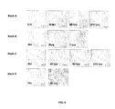
- FIG. 6 shows the optical images of 4 different encapsulation barrier stacks, Stacks A, B, C, and D, after exposure to moisture.
- FIG. 7 shows 70 ⁇ magnification SEM images of 3 encapsulation barrier Stacks A to C made according to the invention.
- FIG. 8 shows the morphology of the 3 encapsulation barrier Stacks A to C made according to the invention.
- FIG. 9 shows an embodiment of the encapsulation barrier stack of the invention comprising a capping acrylic film.
- the encapsulation barrier stack was used for quantitative analysis.
- FIG. 10 shows a graph of Electrical Conductance vs Time for the encapsulation barrier stack shown in FIG. 9 .
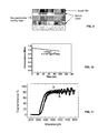
- FIG. 11 shows a graph of Transmittance vs Wavelength for the encapsulation barrier stack shown in FIG. 9 .
- FIG. 12 shows the scanning electron microscopy (SEM) images of barrier stacks D, E and F.
- FIG. 13 shows the graph of transmittance vs. wavelength for encapsulation barrier stacks A, C, D, E and F.
- FIG. 14 shows the graph of Conductance vs. Time for encapsulation barrier stacks D, E and F.
- FIG. 15 shows the Load Strain performance curve for barrier stacks D, G and H.
- FIG. 1A shows one embodiment of an encapsulation barrier stack 100 according to the invention.
- the encapsulation barrier stack 100 comprises a multilayer film 102 comprising barrier layers 103 and sealing layers 105 .
- the barrier layers 103 have low permeability to oxygen and/or moisture.
- barrier layers 103 contain pinhole defects 107 which extend through the thickness of the barrier layer 103 .
- Pinhole defects along with other types of structural defects limit the barrier performance of barrier layers as oxygen and water vapour can permeate into the barrier layer via these defects, eventually traversing the encapsulation barrier stack and coming into contact with the oxygen/moisture sensitive device.
- FIG. 1A depicts only pinhole defects. In reality, other types of structural defects such as pits and cracks may also be present.
- the sealing layers 105 comprise reactive nanoparticles capable of interacting with water vapour and/or oxygen, thereby retarding the permeation of oxygen/moisture through the encapsulation barrier stack. In accordance with the present invention, these defects are at least partially covered up, or in some embodiments, entirely filled up by the nanoparticles in the sealing layer 105 .
- FIG. 1B depicts a conventional barrier stack 120 which comprises barrier layers 123 and planarising adhesive layers 125 are arranged on a substrate 121 .
- inorganic metal oxide barrier layers have relatively high gas impermeability, pinhole defects present in the barrier layer allow moisture and oxygen to permeate through the barrier layer.
- pinhole defects 127 in the barrier layers 123 are exposed to the environment, so moisture and oxygen are able to permeate through the barrier layer.
- oxygen and moisture can permeate through the barrier layer 1231 via pinhole defects, and then progressively permeate through the adhesive layer 1251 , and subsequently permeate through barrier layer 1232 and adhesive layer 1252 to reach the substrate 121 where an oxygen/moisture sensitive device is typically located.
- FIG. 1C depicts yet another embodiment of a barrier stack 140 according to the invention wherein the multilayer film 142 comprises one barrier layer 143 and only one sealing layer 145 arranged over it.
- the barrier stack 140 further comprises a base substrate 141 for supporting the multilayer film.
- a planarising layer 144 is interposed between the base substrate 141 and the multilayer film 142 included to improve the contact between the multilayer film and the substrate.
- a single paired layer in accordance with this embodiment can be used for applications with less stringent barrier requirements.
- FIG. 1D shows a double-laminated substrate in which a multilayer film is laminated to both sides of a base substrate.
- Encapsulation barrier stack 160 comprises a substrate 161 that is sandwiched between two multilayer films 1621 and 1622 .
- Multilayer film 1621 comprises 3 barrier layers 163 and three nanoparticulate sealing layers 165 .
- Multilayer film 1622 comprises 1 barrier layer and 2 sealing layers. Each respective layer is arranged in alternating sequence such that the sealing layers form the interlayer between any 2 barrier layers.
- sealing layers 165 are in direct contact with the substrate 161 , thereby serving as planarising layers.
- the encapsulation barrier stack of the invention can be used in several ways for encapsulating a moisture and oxygen sensitive device such as an OLED.
- a moisture and oxygen sensitive device such as an OLED
- it can be laminated onto a conventional polymer substrate that is used to support the OLED.
- FIG. 2A shows an encapsulated OLED comprising electrodes 214 and reactive layer 216 within a rim-sealed encapsulation.
- the encapsulation barrier stack comprises a base substrate 201 and a multilayer film 212 .
- the base substrate 201 is laminated with the multilayer film 212 comprising barrier layer 203 and two sealing layers 205 sandwiching the barrier layer 203 .
- Pinhole defects 207 in the barrier layer 203 are sealed by the nanoparticulate material of the sealing layer.
- the OLED is arranged directly on the multilayer film 212 , and encapsulated under a glass cover 210 .
- Rim adhesive 209 serves to adhere the glass cover 210 to the encapsulation barrier stack, thereby forming an encapsulation around the OLED.
- FIG. 2B shows another embodiment in which the encapsulation barrier stack of the invention is used as a cover substrate.
- the substrate 201 is not laminated by the encapsulation barrier stack (although it may be laminated if desired).
- the encapsulation barrier stack comprising rigid multilayer film 222 (without a substrate).
- the multilayer film similarly comprises barrier layer 203 sandwiched between sealing layers 205 , and its defects 207 are filled with the nanoparticulate material.
- the OLED is encapsulated underneath the multilayer film, meaning that in order for the light emitted by the OLED to be clearly seen, the multilayer film 222 should be sufficiently transparent.
- the multilayer film 222 is attached to the base substrate by means of rim adhesive 209 .
- the width of the rim adhesive is typically in the millimeter or centimeter scale, which is substantially larger than the thickness of the base substrate or the encapsulation barrier stack. Accordingly, lateral diffusion of water vapour and oxygen through the rim adhesive would in such a case be substantially longer than transverse diffusion through the encapsulated barrier stack.
- FIG. 2C shows an embodiment in which an OLED comprising electrodes 214 and reactive layer 216 is encapsulated between a flexible base substrate 201 and a flexible encapsulation barrier stack arranged proximally over the OLED comprising multilayer film 232 . It will be noted that the multilayer film 232 conforms to the external shape of the OLED device.
- FIGS. 2A, 2B and 2C depict the encapsulation of an OLED
- the encapsulation barrier stack of the present invention is by no means limited to such an application. It will be understood by the skilled person the any article can be encapsulated in place of an OLED, including pharmaceutical drugs, jewelry, reactive metals, electronic components, and food substances, for example.
- FIG. 3 The general scheme of fabrication of the encapsulation barrier stack according to the invention is shown in FIG. 3 .
- a polycarbonate or PET substrate is provided for forming the encapsulation barrier stack.
- the substrate is plasma treated and coated with alumina barrier material via magnetron sputtering, thereby forming a barrier layer.
- a sealing solution comprising alumina and TiO 2 nanoparticles is mixed with an acrylic acid monomer solution, thereby forming a sealing solution.
- the sealing solution is web flight coated onto the barrier layer, for example, via a roll-to-roll process.
- the coating of barrier layer and sealing layer is repeated for a predetermined number of times to obtain a multilayer film with a desired barrier property.
- a multilayer film comprising 5 paired layers will require the magnetron sputtering and web flight coating to be repeated 5 times to form 5 paired layer. It is to be noted that it is also possible, in other embodiments, to form an initial coat of sealing layer over the substrate.
- the sealing layer acts as a planarising material which smoothens the surface of the substrate thereby covering defects on the substrate which could provide pathways for the infiltration of moisture/oxygen.
- ITO is magnetron sputtered over the multilayer film to form an ITO coating.
- ITO lines are required instead of a complete coat of IOT.
- a protective liner is subsequently formed on the ITO coating. Any suitable material may be used, depending on the intended purpose, e.g. scratch resistant films or glare reduction films, such as MgF/LiF films.
- the encapsulation barrier stack is packed in aluminium foil packaging or slit into predetermined dimensions for assembly with other components.
- encapsulation barrier stacks each comprising different nanoparticles in the sealing layer were fabricated.
- Each of the encapsulation barrier stacks were made according to the following specification:
- Stack D comprising a conventional multi-layer stack structure
- Stack D comprised the following stack structure:
- Polycarbonate substrates are transparent and can be cut into preferred dimensions.
- Pneumatically operated hollow die punch-cutting equipment or any conventional slitting machine can be used to slit the polycarbonate substrates into the specified or required dimensions.
- the substrates are rinsed with isopropyl alcohol (IPA) and blow-dried with nitrogen to remove macro-scale adsorbed particles on the surface. After nitrogen blow-dry, the substrates are placed in the vacuum oven at a pressure of 10 ⁇ 1 mbar for degassing absorbed moisture or oxygen.
- IPA isopropyl alcohol
- the substrates are transferred to the plasma treatment chamber (e.g. ULVAC SOLCIET Cluster Tool).
- RF argon plasma is used to bombard the surface of the barrier film with low energy ions in order to remove surface contaminants.
- the base pressure in the chamber was maintained below 4 ⁇ 10 ⁇ 6 mbar.
- the argon flow rate is 70 sccm.
- the RF power is set at 200 W and an optimal treatment time usually 5 to 8 eight minutes is used depending on the surface condition.
- plain acrylic polymer was spin coated onto the polycarbonate substrates to form an interface planarising layer.
- Indium tin oxide barrier layers were prepared by unbalanced magnetron sputtering techniques as follows. Sputtering was used to deposit the metal oxide barrier layer onto the planarising layer. Unbalanced magnetron sputtering technique was used to form high density oxide barrier films. In this sputtering technique, a metal layer of typically a few mono-layers will be deposited from an unbalanced magnetron, and then oxygen will be introduced to the system to create oxygen plasma, directed towards the substrate to provide argon and oxygen ion bombardment for a high packing-density oxide film. Plasma helps to increase the reactivity of the oxygen directed onto the growing film surface and provides for more desirable rheology. In order to deposit dense films without introducing excessive intrinsic stresses, a high flux (greater than 2 mA/cm 2 ) of low energy ( ⁇ 25 eV) oxygen and argon ions to bombard the growing barrier oxide films.
- the continuous feedback control unit is used to control the reactive sputtering processes.
- the light emitted by the sputtering metal in the intense plasma of the magnetron racetrack is one indicator of the metal sputtering rate and the oxygen partial pressure. This indication can be used to control the process and hence achieve an accurate oxide film stoichiometry.
- Nanoparticles e.g. #44931 NanoDur® 99.5% aluminium oxide particles from Nanophase Technologies
- an organic solvent such as 2-methoxyethanol (2MOE) and ethylene glycol (EG) for dispersion in the ratio of 1:1 2MOE to EG.
- 2MOE 2-methoxyethanol
- EG ethylene glycol
- Propylene glycon monomethyl ether or Ethyl Acetate or Methyl Isobutyl Ketone, Methyl Ethyl, 2 MOE or any mixture of solvents or wetting additive agents can be used as well.
- nanoparticle dispersions such as aluminium oxide, zinc oxide, or titanium oxide dispersed in Hexane diol diacrylate, Isobornyl acrylate, Tripropylene glycol diacrylate can be used (e.g. a colloidal dispersion of 45 nm APS aluminum oxide dry powder, NanoDur® X1130PMA, 50% dispersed in 1,2-Propanediol monomethyl ether acetate from Nanophase Technologies).
- a polymerizable group compound like commercially available UV curable acrylate monomers is added to the nanoparticle mixture to form a sealing solution.
- the polymer coating weight may be between the amount of 30% to 50%.
- the total concentration of nanoparticles in the polymer may at 66% by weight of the sealing solution, while polymer coating weight is at about 34% by weight of the sealing solution.
- sample encapsulation barrier stack A 30 ml of UV curable acrylate monomer with a coating weight of about 50% of the sealing solution was added to 15 ml of a dispersion of aluminium oxide in tripropylene glycol diacrylate (35% weight), obtainable from Nanodur of Nanophase Technologies. 5 ml of an organic solvent of 2-MOE and EG (1:1) ratio was added to the mixture. Sonification of the mixture was then carried out for about 1 hour prior to deposition onto a barrier oxide layer.
- sample encapsulation barrier stack B For sample encapsulation barrier stack B, 30 ml of UV curable acrylate monomer with a coating weight of about 50% of the sealing solution was added to 10 ml of titanium (IV) oxide dispersed in isopropanol 40% by weight, obtainable from Nanodur of Nanophase Technologies. 10 ml of an organic solvent of 2-MOE and EG (1:1) ratio was added to the mixture. Sonification of the mixture was then carried for about 1 hour prior to deposition onto a barrier oxide layer.
- sample encapsulation barrier stack C 30 ml of UV curable acrylate monomer with a coating weight of about 50% by weight of the sealing solution was added to (a) 7.5 ml of dispersed aluminium oxide in tripropylene glycol diacrylate (35% weight), obtainable from Nanodur of Nanophase Technologies, and (b) 5 ml of Titanium (IV) oxide dispersed in Isoproanal with 40% weight with 2 MOE and Ethylene glycol (1:1 ratio). Sonification of the mixture was then carried for about 1 hour prior to deposition onto a barrier oxide layer.
- the formation of the sealing layer via spin coating was undertaken in a nitrogen atmosphere in a glove box.
- the oxygen and water vapour contents were reduced to less than 1 ppm level in the glove box.
- the encapsulation barrier stacks are transferred to a vacuum evaporation chamber (thermal evaporation) under vacuum.
- the barrier stacks are then evaluated for their barrier properties using the calcium sensor described in WO 2005/095924. Both qualitative evaluation and quantitative evaluation were carried out.
- a test cell as shown in FIG. 4 is formed using the fabricated encapsulation barrier stacks. Briefly, two metal tracks with dimensions of 2 cm by 2 cm are fabricated. A sensing element having dimensions of 1 cm length, 2 cm width and 150 nm thickness is formed in between the two electrodes. The measured resistivity of the sensing element is 0.37 ⁇ -cm. After the deposition process, a load lock system is used to transfer the sample to a glove box under dry nitrogen at atmospheric pressure. After the calcium deposition, a 100 nm silver protection layer was deposited for the qualitative analysis.
- a test cell as shown in FIG. 5 is formed using the fabricated encapsulation barrier stacks. 300 nm of silver was used for the conductive track, 150 nm calcium was used as the sensor and 150 nm lithium fluoride was used as a protection layer. After the deposition processes, a UV curable epoxy was applied on the rim of the substrate and then the whole substrate was sealed with a 35 mm ⁇ 35 mm glass slide. Desiccants were attached to the 35 mm ⁇ 35 mm cover glass slide for absorbing any water vapour present due to out gassing or permeation through the epoxy sealing. A load lock system was used for the entire process and the test cells were encapsulated in the glove box under dry nitrogen at atmospheric pressure.
- the samples were placed into a humidity chamber at constant temperature and humidity of 80° C. & 90% RH respectively. These were viewed optically at regular intervals for a qualitative degradation test and analysis of the defects, and measured electrically for the quantitative analysis of the degradation.
- the calcium test cell's conductive track terminals are connected to a constant current source (Keithey source meter), which is interfaced with a computer. Resistance of the calcium sensor/silver track is monitored every second and plotted automatically by the computer using lab view software.
- a Dynamic Signal Analyzer with a FFT analysis is used to take the noise spectrum measurement automatically at periodic intervals of one second.
- the calcium degradation test provides qualitative visual information on defects such as pinholes cracks and nano-pores, because the permeated water vapors diffuse through the defects of the substrate and its barrier layer(s) and react with the calcium sensor to form distinguishable patches on the calcium sensing element.
- Micro-pores and sub-micron sized pores such as pinholes and cracks in a transparent coating are very difficult to discern or to study even by sophisticated surface microscopy techniques (e.g. SEM).
- SEM surface microscopy techniques
- the colour contrast between oxidized and non-oxidized calcium was used for qualitative analysis.
- the degradation was monitored using optical microscopy. The images were taken at intervals of typically several hours. From the images the calcium-corroded spots could be directly linked to defects of the barrier films. Further, growth dynamics of the calcium corrosion could provide qualitative information of barrier properties.
- the images in FIG. 6 highlight the nature of the defects exhibited on A B, C films that have been tested and the barrier structure is shown in FIG. 6 .
- the degradation images in FIG. 6 show that the barrier stacks A and C have significantly better barrier properties as compared to conventional barrier stacks as exemplified by barrier stack D.
- Calcium sensor degradation in barrier stack A commenced at 80 hours and the entire calcium degraded by 270 hours. Calcium sensor degradation in barrier stack C did no show any significant degradation until after 470 hours.
- FIG. 7 shows scanning electron microscopy (SEM) images of barrier stacks A, B & C immediately after fabrication.
- SEM scanning electron microscopy
- FIG. 8 shows images of the surface of the sealing layers as studied with SEM and AFM.
- the surface properties were compared with of that of plain acrylic polymer coatings.
- the AFM picture shows that the uniform dispersion of nanoparticles in solution A, B and C was achieved.
- the surface roughness measured for barrier stacks A and B films are well within 0.75 nm at 1 ⁇ m to 10 ⁇ m scans and comparable with plain acrylic polymer films.
- the surface is relatively rough (6.5 nm). Roughness may be advantageously used to improve the adhesion between the barrier layer and the substrate.
- a test encapsulation barrier stack having the structure shown in FIG. 9 was fabricated to carry out a quantitative analysis of the encapsulation barrier stack samples fabricated in accordance with the above.
- An encapsulation barrier stack was fabricated with two ITO barrier layers were fabricated by magnetron sputtering method and one sealing layer (comprising aluminium oxide nanoparticles) was used to seal the ITO defects.
- the outermost terminating layer is plain acrylic film which is normally used for WVTR measurement purpose. In principle, only one ITO barrier layer's defects were sealed.
- the sealing layer comprises Al 2 O 3 nanoparticles with sizes of 20 nm to 40 nm.
- the plot of calcium conductance against time is shown in FIG. 10 for the encapsulation barrier stack.
- the corresponding change in calcium (mol) can be derived from the graph.
- the water vapour transmission rate of the encapsulation barrier stack comprising one barrier layer and one sealing layer is determined to be 1 ⁇ 10 ⁇ 3 g/m 2 /day at 80° C. & 90% relative humidity.
- conventional multi-layer stacks with two barriers SiN layer and plain acrylic interlayer showed performance of only about 10 ⁇ 1 g/m 2 /day level at 70° C. & 90% relative humidity condition.
- the barrier performance is improved up to two orders in higher magnitude as compared to the plain acrylic film based multi-layer substrate. If the defects in three or more barrier layers are sealed using two or more sealing layers comprising reactive nanoparticles, the water vapour barrier performance can be less than 10 ⁇ 5 g/m 2 /day, or even less than 10 ⁇ 6 g/m 2 /day.
- the single-layered encapsulation barrier stack comprising polycarbonate (188 ⁇ m)/ITO/Nanostructured sealing layer with aluminium and titanium nanoparticle and the double-layered encapsulation barrier stack with PC/ITO/sealing layer/ITO/sealing layer was fabricated.
- the optical properties measured the spectral transmission in the UV and visible region of the spectrum was measured with UV-Vis spectrometer. It shows that the light transmittance of double stack is 82% and single stack is about 85%. The reduction of transmission is due to ITO film properties and nature.
- MCNT Pre-treated 10 nm diameter multiwalled nanotubes
- 2MOE 2-methoxyethanol
- EG ethylene glycol
- the ratio of 2MOE to EG is 1:1.
- the nanotubes were dispersed uniformly into the acrylic polymer via sonification. The synthesis was undertaken under inert gas environment.
- Stack E comprises MCNT in the amount of 0.006% by weight
- solution F comprises MCNT in the amount of 0.05% by weight.
- the sealing layers were 2 ⁇ m thick. The synthesis and fabrication of thin films of sealing layers were under taken in the glove box which has partial pressure of nitrogen. The oxygen and water vapour contents were controlled with less than 1 ppm level in the glove box.
- Stack D as fabricated in Example 1 was used for the comparison of the characteristics of the barrier stacks E and F.
- FIG. 12 shows scanning electron microscopy (SEM) images of Stacks D, E & F films.
- SEM scanning electron microscopy
- each barrier stack was measured with spectral transmission in the UV and visible region of the spectrum with UV-Vis Spectrometry.
- conventional acrylic film coated substrate (D) has very high transmission with 99%. However, it does not block UV light. It shows that the light transmittance of double stack is 82% and single stacks are about 85%.
- the CNT contained encapsulation barrier stack E & F shows transparency about 85%. The reduction of double stack transmission is due to ITO film properties and nature.
- the figure also shows that the nanoparticle dispersion of the films A, C, E & F are uniform, have no agglomeration and therefore, the light transmission is in the range of 82 to 89%.
- the quantitative calcium degradation results of FIG. 14 show that the barrier stack E and barrier stack F shows significantly better overall barrier properties than conventional barrier stack D.
- the CNT-containing encapsulation barrier stacks E and F shows the rates of 0.01 g/m 2 /day and 0.009 g/m 2 /day level respectively. After reaching 100 hrs, the barrier stacks E and F shows a significant improvement in barrier properties and the WVTR rates was 0.003 g/m 2 /day.
- barrier stacks E and F water vapour is drawn into open-ended nanotubes by capillary suction after 30 hrs of exposure. It is postulated that the time taken for the water molecule to diffuse into the carbon nanotubes is longer as compared to normal modes of diffusion and therefore, the initial water vapour desorption was very high.
- the initial desorption/permeability results of this invention demonstrated that the probability of sealing the defects of the barrier layer by CNTs is relatively low. This may be due to the concentration (0.05%) of CNT used in the interlayer as compared to the nanoparticles concentration (30% to 60%).
- Example 1 Conventional barrier stack D as fabricated in Example 1 was again used for comparison.
- the 2 ⁇ m thick sealing layers were deposited onto ITO coated polycarbonate test substrates and these substrates. They were cut into the pieces of 10 cm length and 1 cm width and the UV curable epoxy (Three Bond) were applied to a 3 cm long and 1 cm wide area at one end of the sample similar to the ASTM requirements.
- Surface preparation involves the argon plasma cleaning of the above substrates before the application of epoxy.
- the Load/Strain curve for sample barrier stacks D, G and H were plotted and the results of the test can be seen in FIG. 15 .
- the barrier stacks D with the plain conventional acrylic film on ITO surface the initial interfacial failure occurred at the interface between the acrylic film and ITO at 18 N/m and levelling off to steady-state peel strength of about 12 N/m. Therefore the adhesion strength of conventional acrylic polymer onto barrier oxide layer is only 18 N/m.
- the initial interfacial failure occurred at the interface between the nanostructured organic sealing layer and ITO at 45 N/m for barrier stacks H and 48 N/m for barrier stacks G and levelling off to steady-state peel strength of about 14-15 N/m for barrier stacks H and G.
Landscapes
- Chemical & Material Sciences (AREA)
- Engineering & Computer Science (AREA)
- Nanotechnology (AREA)
- Physics & Mathematics (AREA)
- Optics & Photonics (AREA)
- Crystallography & Structural Chemistry (AREA)
- Inorganic Chemistry (AREA)
- Life Sciences & Earth Sciences (AREA)
- Materials Engineering (AREA)
- General Physics & Mathematics (AREA)
- Condensed Matter Physics & Semiconductors (AREA)
- Composite Materials (AREA)
- Health & Medical Sciences (AREA)
- General Health & Medical Sciences (AREA)
- Molecular Biology (AREA)
- Organic Chemistry (AREA)
- Biophysics (AREA)
- Electroluminescent Light Sources (AREA)
- Laminated Bodies (AREA)
- Packages (AREA)
- Wrappers (AREA)
Priority Applications (1)
| Application Number | Priority Date | Filing Date | Title |
|---|---|---|---|
| US15/289,074 US20170098799A1 (en) | 2006-11-06 | 2016-10-07 | Nanoparticulate encapsulation barrier stack |
Applications Claiming Priority (1)
| Application Number | Priority Date | Filing Date | Title |
|---|---|---|---|
| PCT/SG2006/000334 WO2008057045A1 (en) | 2006-11-06 | 2006-11-06 | Nanoparticulate encapsulation barrier stack |
Related Parent Applications (1)
| Application Number | Title | Priority Date | Filing Date |
|---|---|---|---|
| PCT/SG2006/000334 A-371-Of-International WO2008057045A1 (en) | 2006-11-06 | 2006-11-06 | Nanoparticulate encapsulation barrier stack |
Related Child Applications (1)
| Application Number | Title | Priority Date | Filing Date |
|---|---|---|---|
| US15/289,074 Continuation US20170098799A1 (en) | 2006-11-06 | 2016-10-07 | Nanoparticulate encapsulation barrier stack |
Publications (2)
| Publication Number | Publication Date |
|---|---|
| US20100089636A1 US20100089636A1 (en) | 2010-04-15 |
| US9493348B2 true US9493348B2 (en) | 2016-11-15 |
Family
ID=39364772
Family Applications (2)
| Application Number | Title | Priority Date | Filing Date |
|---|---|---|---|
| US12/513,569 Expired - Fee Related US9493348B2 (en) | 2006-11-06 | 2006-11-06 | Nanoparticulate encapsulation barrier stack |
| US15/289,074 Abandoned US20170098799A1 (en) | 2006-11-06 | 2016-10-07 | Nanoparticulate encapsulation barrier stack |
Family Applications After (1)
| Application Number | Title | Priority Date | Filing Date |
|---|---|---|---|
| US15/289,074 Abandoned US20170098799A1 (en) | 2006-11-06 | 2016-10-07 | Nanoparticulate encapsulation barrier stack |
Country Status (10)
| Country | Link |
|---|---|
| US (2) | US9493348B2 (pl) |
| EP (1) | EP2082619B1 (pl) |
| JP (1) | JP5559542B2 (pl) |
| KR (1) | KR101130199B1 (pl) |
| CN (1) | CN101518151B (pl) |
| AU (1) | AU2006350626B2 (pl) |
| ES (1) | ES2935269T3 (pl) |
| PL (1) | PL2082619T3 (pl) |
| TW (1) | TWI479940B (pl) |
| WO (1) | WO2008057045A1 (pl) |
Cited By (10)
| Publication number | Priority date | Publication date | Assignee | Title |
|---|---|---|---|---|
| US20150351167A1 (en) * | 2014-05-30 | 2015-12-03 | Samsung Sdi Co., Ltd. | Encapsulated device having edge seal and methods of making the same |
| US20170098799A1 (en) * | 2006-11-06 | 2017-04-06 | Agency For Science, Technology And Research | Nanoparticulate encapsulation barrier stack |
| US9660218B2 (en) * | 2009-09-15 | 2017-05-23 | Industrial Technology Research Institute | Package of environmental sensitive element |
| US10538841B2 (en) | 2014-08-07 | 2020-01-21 | Toyo Seikan Group Holdings, Ltd. | Water-barrier laminate |
| US10556411B2 (en) | 2015-08-18 | 2020-02-11 | Toyo Seikan Group Holdings, Ltd. | Water barrier laminate |
| US10683432B2 (en) | 2014-08-07 | 2020-06-16 | Toyo Seikan Group Holdings, Ltd. | Coating composition |
| US11532763B2 (en) | 2012-11-06 | 2022-12-20 | Oti Lumionics Inc. | Method for depositing a conductive coating on a surface |
| US11825691B2 (en) * | 2017-04-17 | 2023-11-21 | Boe Technology Group Co., Ltd. | Display panel and water-absorbing magnetic nanoparticles |
| US11963377B2 (en) | 2019-11-06 | 2024-04-16 | Applied Materials, Inc. | Light-emitting diode light extraction layer having graded index of refraction |
| US11974457B2 (en) | 2020-01-22 | 2024-04-30 | Applied Materials, Inc. | Light-emitting diode display devices with mirror |
Families Citing this family (180)
| Publication number | Priority date | Publication date | Assignee | Title |
|---|---|---|---|---|
| US9079246B2 (en) | 2009-12-08 | 2015-07-14 | Baker Hughes Incorporated | Method of making a nanomatrix powder metal compact |
| US9682425B2 (en) | 2009-12-08 | 2017-06-20 | Baker Hughes Incorporated | Coated metallic powder and method of making the same |
| US9109429B2 (en) | 2002-12-08 | 2015-08-18 | Baker Hughes Incorporated | Engineered powder compact composite material |
| US8327931B2 (en) | 2009-12-08 | 2012-12-11 | Baker Hughes Incorporated | Multi-component disappearing tripping ball and method for making the same |
| US9101978B2 (en) | 2002-12-08 | 2015-08-11 | Baker Hughes Incorporated | Nanomatrix powder metal compact |
| US8403037B2 (en) | 2009-12-08 | 2013-03-26 | Baker Hughes Incorporated | Dissolvable tool and method |
| US8297364B2 (en) | 2009-12-08 | 2012-10-30 | Baker Hughes Incorporated | Telescopic unit with dissolvable barrier |
| JP5308353B2 (ja) * | 2006-12-28 | 2013-10-09 | エージェンシー フォー サイエンス,テクノロジー アンド リサーチ | 集積化気体透過センサを有するカプセル化デバイス |
| JP4694519B2 (ja) * | 2007-02-28 | 2011-06-08 | 富士通株式会社 | マイクロ構造体およびマイクロ構造体製造方法 |
| KR101964265B1 (ko) | 2008-04-09 | 2019-07-31 | 에이전시 포 사이언스, 테크놀로지 앤드 리서치 | 산소 및/또는 수분 민감성 전자 소자들을 밀봉하는 다층막 |
| KR101549530B1 (ko) * | 2008-05-23 | 2015-09-02 | 가부시키가이샤 한도오따이 에네루기 켄큐쇼 | 반도체장치 |
| FR2936651B1 (fr) * | 2008-09-30 | 2011-04-08 | Commissariat Energie Atomique | Dispositif optoelectronique organique et son procede d'encapsulation. |
| JP2010140980A (ja) * | 2008-12-10 | 2010-06-24 | Sony Corp | 機能性有機物素子及び機能性有機物装置 |
| ITMI20082206A1 (it) * | 2008-12-12 | 2010-06-13 | Getters Spa | Materiale composito per la protezione di dispositivi sensibili ad h2o costituito da nanozeoliti disperse in una matrice polimerica |
| DE102009018518A1 (de) | 2009-04-24 | 2010-10-28 | Tesa Se | Transparente Barrierelaminate |
| US9034663B2 (en) | 2009-05-27 | 2015-05-19 | Koninklijke Philips N.V. | Sealed thin-film device, method of and system for repairing a sealing layer applied to a thin-film device |
| WO2010140980A1 (en) | 2009-06-02 | 2010-12-09 | Agency For Science, Technology And Research | Multilayer barrier film |
| EP2273579A1 (en) * | 2009-07-10 | 2011-01-12 | Nederlandse Organisatie voor toegepast -natuurwetenschappelijk onderzoek TNO | A method of encapsulating a flexible optoelectronic multi-layered structure |
| FR2949776B1 (fr) | 2009-09-10 | 2013-05-17 | Saint Gobain Performance Plast | Element en couches pour l'encapsulation d'un element sensible |
| FR2949775B1 (fr) | 2009-09-10 | 2013-08-09 | Saint Gobain Performance Plast | Substrat de protection pour dispositif collecteur ou emetteur de rayonnement |
| KR101084230B1 (ko) * | 2009-11-16 | 2011-11-16 | 삼성모바일디스플레이주식회사 | 유기 발광 표시 장치 및 유기 발광 표시 장치의 제조 방법 |
| US8573295B2 (en) | 2010-11-16 | 2013-11-05 | Baker Hughes Incorporated | Plug and method of unplugging a seat |
| US9127515B2 (en) | 2010-10-27 | 2015-09-08 | Baker Hughes Incorporated | Nanomatrix carbon composite |
| US9227243B2 (en) | 2009-12-08 | 2016-01-05 | Baker Hughes Incorporated | Method of making a powder metal compact |
| US8528633B2 (en) | 2009-12-08 | 2013-09-10 | Baker Hughes Incorporated | Dissolvable tool and method |
| US10240419B2 (en) | 2009-12-08 | 2019-03-26 | Baker Hughes, A Ge Company, Llc | Downhole flow inhibition tool and method of unplugging a seat |
| US9243475B2 (en) | 2009-12-08 | 2016-01-26 | Baker Hughes Incorporated | Extruded powder metal compact |
| US8425651B2 (en) | 2010-07-30 | 2013-04-23 | Baker Hughes Incorporated | Nanomatrix metal composite |
| JP5290268B2 (ja) | 2009-12-31 | 2013-09-18 | 三星ディスプレイ株式會社 | バリア・フィルム複合体、これを含む表示装置、バリア・フィルム複合体の製造方法、及びこれを含む表示装置の製造方法 |
| KR101213499B1 (ko) * | 2009-12-31 | 2012-12-20 | 삼성디스플레이 주식회사 | 배리어 필름 복합체, 이를 포함하는 표시 장치 |
| KR20170003711A (ko) * | 2009-12-31 | 2017-01-09 | 생-고뱅 어브레이시브즈, 인코포레이티드 | 포장된 연마물품 및 그 제조방법 |
| JP5611811B2 (ja) * | 2009-12-31 | 2014-10-22 | 三星ディスプレイ株式會社Samsung Display Co.,Ltd. | バリア・フィルム複合体及びこれを含む表示装置 |
| JP5611812B2 (ja) * | 2009-12-31 | 2014-10-22 | 三星ディスプレイ株式會社Samsung Display Co.,Ltd. | バリア・フィルム複合体、これを含む表示装置及び表示装置の製造方法 |
| US8424610B2 (en) | 2010-03-05 | 2013-04-23 | Baker Hughes Incorporated | Flow control arrangement and method |
| US9175397B2 (en) * | 2010-03-15 | 2015-11-03 | Alliance For Sustainable Energy, Llc | Multilayer heterostructures and their manufacture |
| ITMI20100080U1 (it) | 2010-03-22 | 2011-09-23 | Getters Spa | Composizione per la protezione di dispositivi sensibili alla presenza di h2o. |
| US8512809B2 (en) * | 2010-03-31 | 2013-08-20 | General Electric Company | Method of processing multilayer film |
| KR101798487B1 (ko) * | 2010-06-01 | 2017-11-17 | 삼성디스플레이 주식회사 | 표시 장치 |
| GB2481367B (en) * | 2010-06-04 | 2015-01-14 | Plastic Logic Ltd | Moisture Barrier for Electronic Devices |
| KR101201720B1 (ko) * | 2010-07-29 | 2012-11-15 | 삼성디스플레이 주식회사 | 표시 장치 및 유기 발광 표시 장치 |
| US8776884B2 (en) | 2010-08-09 | 2014-07-15 | Baker Hughes Incorporated | Formation treatment system and method |
| US9090955B2 (en) | 2010-10-27 | 2015-07-28 | Baker Hughes Incorporated | Nanomatrix powder metal composite |
| WO2012063445A1 (ja) * | 2010-11-12 | 2012-05-18 | シャープ株式会社 | 有機el表示装置およびその製造方法 |
| US20120132272A1 (en) | 2010-11-19 | 2012-05-31 | Alliance For Sustainable Energy, Llc. | Solution processed metal oxide thin film hole transport layers for high performance organic solar cells |
| US20120142140A1 (en) * | 2010-12-02 | 2012-06-07 | Applied Nanotech Holdings, Inc. | Nanoparticle inks for solar cells |
| DE102010056562B4 (de) | 2010-12-30 | 2018-10-11 | Snaptrack, Inc. | Elektroakustisches Bauelement und Verfahren zur Herstellung des elektroakustischen Bauelements |
| DE102010056572B4 (de) | 2010-12-30 | 2018-12-27 | Snaptrack, Inc. | Elektronisches Bauelement und Verfahren zur Herstellung des elektronischen Bauelements |
| MY161553A (en) * | 2011-01-27 | 2017-04-28 | Vitriflex Inc | An inorganic multilayer stack and methods and compositions relating thereto |
| DE102011005612A1 (de) * | 2011-03-16 | 2012-09-20 | Osram Opto Semiconductors Gmbh | Organisches Optoelektronisches Bauelement und Verfahren zur Herstellung eines Optoelektronischen Bauelements |
| FR2973939A1 (fr) | 2011-04-08 | 2012-10-12 | Saint Gobain | Element en couches pour l’encapsulation d’un element sensible |
| FR2973940A1 (fr) * | 2011-04-08 | 2012-10-12 | Saint Gobain | Element en couches pour l’encapsulation d’un element sensible |
| US8631876B2 (en) | 2011-04-28 | 2014-01-21 | Baker Hughes Incorporated | Method of making and using a functionally gradient composite tool |
| US9080098B2 (en) | 2011-04-28 | 2015-07-14 | Baker Hughes Incorporated | Functionally gradient composite article |
| US9633819B2 (en) * | 2011-05-13 | 2017-04-25 | Fibics Incorporated | Microscopy imaging method and system |
| JP5735857B2 (ja) * | 2011-05-23 | 2015-06-17 | 株式会社サムスン日本研究所 | 電子デバイス用バリアフィルム |
| US20120299162A1 (en) * | 2011-05-23 | 2012-11-29 | Samsung Electronics Co. Ltd. | Barrier film for electronic device, method of manufacture thereof, and articles including the same |
| US9139928B2 (en) | 2011-06-17 | 2015-09-22 | Baker Hughes Incorporated | Corrodible downhole article and method of removing the article from downhole environment |
| US9219182B2 (en) | 2011-07-06 | 2015-12-22 | Dow Global Technologies Llc | Optoelectronic devices incorporating fluoropolymer compositions for protection |
| US9707739B2 (en) | 2011-07-22 | 2017-07-18 | Baker Hughes Incorporated | Intermetallic metallic composite, method of manufacture thereof and articles comprising the same |
| US9643250B2 (en) | 2011-07-29 | 2017-05-09 | Baker Hughes Incorporated | Method of controlling the corrosion rate of alloy particles, alloy particle with controlled corrosion rate, and articles comprising the particle |
| US9833838B2 (en) | 2011-07-29 | 2017-12-05 | Baker Hughes, A Ge Company, Llc | Method of controlling the corrosion rate of alloy particles, alloy particle with controlled corrosion rate, and articles comprising the particle |
| EP2742537A4 (en) | 2011-08-04 | 2015-05-20 | 3M Innovative Properties Co | LOCKING DEVICE WITH EDGE PROTECTION |
| SG2014007892A (en) * | 2011-08-04 | 2014-04-28 | 3M Innovative Properties Co | Method of making delamination resistant assemblies |
| US9033055B2 (en) | 2011-08-17 | 2015-05-19 | Baker Hughes Incorporated | Selectively degradable passage restriction and method |
| US9856547B2 (en) | 2011-08-30 | 2018-01-02 | Bakers Hughes, A Ge Company, Llc | Nanostructured powder metal compact |
| US9090956B2 (en) | 2011-08-30 | 2015-07-28 | Baker Hughes Incorporated | Aluminum alloy powder metal compact |
| US9109269B2 (en) | 2011-08-30 | 2015-08-18 | Baker Hughes Incorporated | Magnesium alloy powder metal compact |
| US9643144B2 (en) | 2011-09-02 | 2017-05-09 | Baker Hughes Incorporated | Method to generate and disperse nanostructures in a composite material |
| US9133695B2 (en) | 2011-09-03 | 2015-09-15 | Baker Hughes Incorporated | Degradable shaped charge and perforating gun system |
| US9347119B2 (en) | 2011-09-03 | 2016-05-24 | Baker Hughes Incorporated | Degradable high shock impedance material |
| US9187990B2 (en) | 2011-09-03 | 2015-11-17 | Baker Hughes Incorporated | Method of using a degradable shaped charge and perforating gun system |
| EP3593992A1 (en) * | 2011-10-24 | 2020-01-15 | Tera-Barrier Films Pte Ltd | Encapsulation barrier stack |
| US9284812B2 (en) | 2011-11-21 | 2016-03-15 | Baker Hughes Incorporated | System for increasing swelling efficiency |
| CN103137885A (zh) * | 2011-11-25 | 2013-06-05 | 海洋王照明科技股份有限公司 | 一种有机电致发光器件的复合封装结构及其封装方法 |
| CN103137883B (zh) * | 2011-11-25 | 2016-06-01 | 海洋王照明科技股份有限公司 | 一种有机电致发光器件的复合封装结构及其封装方法 |
| CN103137886A (zh) * | 2011-11-25 | 2013-06-05 | 海洋王照明科技股份有限公司 | 一种有机电致发光器件的复合封装结构及其封装方法 |
| CN103137648A (zh) * | 2011-12-05 | 2013-06-05 | 联胜(中国)科技有限公司 | 电致发光显示装置 |
| US8999497B2 (en) * | 2011-12-13 | 2015-04-07 | Samsung Electronics Co., Ltd. | Barrier film for electronic device and method of manufacturing the same |
| TWI429526B (zh) * | 2011-12-15 | 2014-03-11 | Ind Tech Res Inst | 水氣阻障複合膜及封裝結構 |
| KR101454101B1 (ko) * | 2012-01-06 | 2014-10-27 | 주식회사 엘지화학 | 전자장치의 제조방법 |
| US9010416B2 (en) | 2012-01-25 | 2015-04-21 | Baker Hughes Incorporated | Tubular anchoring system and a seat for use in the same |
| US9068428B2 (en) | 2012-02-13 | 2015-06-30 | Baker Hughes Incorporated | Selectively corrodible downhole article and method of use |
| US9362527B2 (en) | 2012-02-15 | 2016-06-07 | Konica Minolta, Inc. | Functional film having a hybrid layer of polysiloxane and fine resin particles |
| CN104169386B (zh) * | 2012-03-12 | 2016-10-26 | Lg化学株式会社 | 压敏性粘合剂组合物 |
| US20150064401A1 (en) * | 2012-04-02 | 2015-03-05 | Konica Minolta, Inc. | Gas barrier film and electronic device |
| KR20130124844A (ko) * | 2012-05-07 | 2013-11-15 | 삼성디스플레이 주식회사 | 표시 장치 및 그 제조 방법 |
| US9605508B2 (en) | 2012-05-08 | 2017-03-28 | Baker Hughes Incorporated | Disintegrable and conformable metallic seal, and method of making the same |
| US9486896B2 (en) | 2012-06-28 | 2016-11-08 | Saint-Gobain Abrasives, Inc. | Abrasive article and coating |
| US10559777B2 (en) | 2012-07-19 | 2020-02-11 | Basf Coatings Gmbh | Radiation curable composition for water scavenging layer, and method of manufacturing the same |
| KR20150101985A (ko) * | 2012-08-31 | 2015-09-04 | 비트리플렉스, 아이엔씨. | 신규한 배리어 층 스택 및 방법 및 이의 조성물 |
| CN104521323B (zh) * | 2012-09-04 | 2016-12-07 | 夏普株式会社 | 有机电致发光显示装置及其制造方法 |
| DE102012109207B4 (de) | 2012-09-28 | 2018-05-09 | Osram Oled Gmbh | Verfahren und Vorrichtung zum Herstellen eines optoelektronischen Bauelementes |
| EP2909027B1 (en) * | 2012-10-18 | 2019-10-09 | Tera-Barrier Films Pte Ltd | Encapsulation barrier stack |
| CN104903098B (zh) * | 2012-11-29 | 2016-12-07 | Lg化学株式会社 | 具有包含无机颗粒的保护涂层的气体阻隔膜 |
| US20150337440A1 (en) * | 2012-11-29 | 2015-11-26 | Lg Chem, Ltd. | Coating method for decreasing damage of barrier layer |
| CN103855308B (zh) * | 2012-11-30 | 2016-04-27 | 海洋王照明科技股份有限公司 | 一种有机电致发光器件及其制备方法 |
| US11141752B2 (en) | 2012-12-27 | 2021-10-12 | Kateeva, Inc. | Techniques for arrayed printing of a permanent layer with improved speed and accuracy |
| CN107757153B (zh) | 2012-12-27 | 2020-05-01 | 科迪华公司 | 用于打印油墨体积控制以在精确公差内沉积流体的技术 |
| US9196849B2 (en) * | 2013-01-09 | 2015-11-24 | Research & Business Foundation Sungkyunkwan University | Polymer/inorganic multi-layer encapsulation film |
| US9676171B2 (en) | 2013-02-07 | 2017-06-13 | Toyo Seikan Group Holdings, Ltd. | Gas barrier laminate having excellent water barrier property |
| US9859515B2 (en) | 2013-03-07 | 2018-01-02 | Alliance For Sustainable Energy, Llc | Methods for producing thin film charge selective transport layers |
| JPWO2014141330A1 (ja) | 2013-03-13 | 2017-02-16 | パナソニック株式会社 | 電子デバイス |
| SG11201508014WA (en) * | 2013-05-02 | 2015-10-29 | Tera Barrier Films Pte Ltd | Encapsulation barrier stack comprising dendrimer encapsulated nanop articles |
| JP2015023055A (ja) * | 2013-07-16 | 2015-02-02 | ソニー株式会社 | 電子装置、光ディスク装置、表示装置および撮像装置 |
| KR102080752B1 (ko) * | 2013-07-23 | 2020-02-25 | 삼성디스플레이 주식회사 | 봉지 구조물, 봉지 구조물을 포함하는 유기 발광 표시장치 및 유기 발광 표시장치의 제조 방법 |
| TWI504513B (zh) * | 2013-08-02 | 2015-10-21 | Innolux Corp | 可撓性顯示裝置 |
| CN103440824B (zh) * | 2013-08-07 | 2016-08-10 | 北京京东方光电科技有限公司 | 一种有机电致发光显示面板、其制造方法及显示装置 |
| US9816339B2 (en) | 2013-09-03 | 2017-11-14 | Baker Hughes, A Ge Company, Llc | Plug reception assembly and method of reducing restriction in a borehole |
| TWI503448B (zh) * | 2013-09-06 | 2015-10-11 | Kingstone Energy Technology Corp | 一種有機與無機複合多層薄膜的製造方法 |
| KR102116497B1 (ko) | 2013-09-25 | 2020-05-29 | 삼성디스플레이 주식회사 | 유기발광 디스플레이 장치 및 그 제조방법 |
| CN105518895B (zh) * | 2013-09-30 | 2017-08-01 | 株式会社Lg化学 | 用于有机电子器件的基板及其制造方法 |
| JP6519974B2 (ja) * | 2013-10-10 | 2019-05-29 | 東洋製罐グループホールディングス株式会社 | 水分バリア性の良好なガスバリア性積層体 |
| FR3012345B1 (fr) | 2013-10-29 | 2017-07-28 | Commissariat Energie Atomique | Dispositif d'encapsulation d'un dispositif sensible et procede de realisation dudit dispositif |
| JP6363707B2 (ja) | 2013-12-12 | 2018-07-25 | カティーバ, インコーポレイテッド | ハーフトーニングを用いて厚さを制御するインクベース層加工 |
| US9156678B2 (en) * | 2013-12-12 | 2015-10-13 | Qualcomm Mems Technologies, Inc. | MEMS encapsulation by multilayer film lamination |
| WO2015112122A1 (en) * | 2014-01-21 | 2015-07-30 | Empire Technology Development Llc | Graphene membranes and methods for making and using the same |
| GB2522626A (en) * | 2014-01-29 | 2015-08-05 | Nokia Technologies Oy | Apparatus and method for providing barrier coating |
| US10689740B2 (en) | 2014-04-18 | 2020-06-23 | Terves, LLCq | Galvanically-active in situ formed particles for controlled rate dissolving tools |
| US11167343B2 (en) | 2014-02-21 | 2021-11-09 | Terves, Llc | Galvanically-active in situ formed particles for controlled rate dissolving tools |
| WO2015127174A1 (en) | 2014-02-21 | 2015-08-27 | Terves, Inc. | Fluid activated disintegrating metal system |
| EP2911213A1 (en) * | 2014-02-24 | 2015-08-26 | Nederlandse Organisatie voor toegepast- natuurwetenschappelijk onderzoek TNO | Method of and apparatus for manufacturing a flexible electronic device |
| CN111081734A (zh) | 2014-03-17 | 2020-04-28 | 松下电器产业株式会社 | 薄膜晶体管元件基板及其制造方法、和有机el显示装置 |
| CN103972422B (zh) * | 2014-04-29 | 2015-04-15 | 京东方科技集团股份有限公司 | 有机电致发光器件的封装结构及封装方法、显示装置 |
| JP2016005900A (ja) * | 2014-05-27 | 2016-01-14 | パナソニックIpマネジメント株式会社 | ガスバリア膜、ガスバリア膜付きフィルム基板およびこれを備えた電子デバイス。 |
| CN104037196B (zh) * | 2014-05-29 | 2017-06-27 | 京东方科技集团股份有限公司 | 一种发光显示面板及其制作方法 |
| DE102014010241A1 (de) | 2014-05-30 | 2015-12-03 | Schott Ag | Körper, bevorzugt mit einer Oberfläche umfassend bevorzugt einen Glaskörper mit einer Glasoberfläche und Verfahren zur Herstellung desselben |
| CN105218099B (zh) * | 2014-06-17 | 2017-08-29 | 苏州图纳新材料科技有限公司 | 一种非极性碳化锆液相陶瓷前驱体及其制备方法和应用 |
| CN104070742A (zh) * | 2014-06-17 | 2014-10-01 | 中国科学院广州能源研究所 | 一种阻隔水汽和防氧渗透的薄膜 |
| JP2016031889A (ja) | 2014-07-30 | 2016-03-07 | 株式会社ジャパンディスプレイ | 表示装置、及びその製造方法 |
| JP5901808B2 (ja) | 2014-08-05 | 2016-04-13 | 古河電気工業株式会社 | 電子デバイス封止用硬化性吸湿性樹脂組成物、封止樹脂および電子デバイス |
| CN105336870B (zh) * | 2014-08-06 | 2017-07-07 | 上海和辉光电有限公司 | 柔性基板及其制造方法 |
| WO2016096937A1 (en) * | 2014-12-18 | 2016-06-23 | Rolic Ag | Radiation curable composition comprising hydrophilic nanoparticles |
| EP3034548A1 (en) * | 2014-12-18 | 2016-06-22 | Nederlandse Organisatie voor toegepast- natuurwetenschappelijk onderzoek TNO | Barrier film laminate comprising submicron getter particles and electronic device comprising such a laminate |
| WO2016109734A1 (en) | 2014-12-30 | 2016-07-07 | Saint-Gobain Abrasives, Inc. | Abrasive tools and methods for forming same |
| US9910026B2 (en) | 2015-01-21 | 2018-03-06 | Baker Hughes, A Ge Company, Llc | High temperature tracers for downhole detection of produced water |
| US10378303B2 (en) | 2015-03-05 | 2019-08-13 | Baker Hughes, A Ge Company, Llc | Downhole tool and method of forming the same |
| KR20160116155A (ko) * | 2015-03-26 | 2016-10-07 | 삼성디스플레이 주식회사 | 유기 발광 표시 장치 |
| CN107531008A (zh) | 2015-05-05 | 2018-01-02 | 纳米碳股份有限公司 | 用于机械增强多层透明导电层状堆叠体的基于碳纳米管的杂化膜 |
| CN104795433B (zh) * | 2015-05-08 | 2016-07-13 | 京东方科技集团股份有限公司 | 显示面板及其制作方法、显示装置 |
| US10221637B2 (en) | 2015-08-11 | 2019-03-05 | Baker Hughes, A Ge Company, Llc | Methods of manufacturing dissolvable tools via liquid-solid state molding |
| KR20170019597A (ko) * | 2015-08-12 | 2017-02-22 | 엘지전자 주식회사 | 태양 전지 및 그 제조 방법 |
| KR102579723B1 (ko) | 2015-08-17 | 2023-09-15 | 쓰리엠 이노베이티브 프로퍼티즈 컴파니 | 나노점토 충전된 배리어 접착제 조성물 |
| CN107925010B (zh) | 2015-08-17 | 2020-11-06 | 3M创新有限公司 | 阻挡膜构造 |
| US9812667B2 (en) | 2015-11-04 | 2017-11-07 | Microsoft Technology Licensing, Llc | Patterning of OLED display stacks |
| KR20180082510A (ko) * | 2015-11-11 | 2018-07-18 | 쓰리엠 이노베이티브 프로퍼티즈 캄파니 | 배리어 층 및 밀봉 층을 포함하는 다층 구조물 |
| JP2019010734A (ja) * | 2015-11-24 | 2019-01-24 | コニカミノルタ株式会社 | 積層型ガスバリアー性フィルム及び電子デバイス |
| JPWO2017094087A1 (ja) * | 2015-11-30 | 2018-09-13 | パイオニア株式会社 | 発光装置 |
| US10016810B2 (en) | 2015-12-14 | 2018-07-10 | Baker Hughes, A Ge Company, Llc | Methods of manufacturing degradable tools using a galvanic carrier and tools manufactured thereof |
| CN108431981B (zh) * | 2015-12-16 | 2022-05-24 | Oti领英有限公司 | 用于光电子器件的屏障涂层 |
| BR112018013258A2 (pt) | 2015-12-30 | 2018-12-11 | Saint Gobain Abrasifs Sa | ferramentas abrasivas e métodos para formar as mesmas |
| CN105514286B (zh) * | 2016-01-08 | 2019-01-04 | 中国计量学院 | 一种基于氟化锂缓冲层的光敏有机场效应管薄膜封装技术 |
| CN105514274B (zh) * | 2016-01-08 | 2019-10-01 | 中国计量学院 | 一种基于氟化锂/聚乙烯醇交替薄膜的有机半导体器件薄膜封装技术 |
| US10287400B2 (en) | 2016-04-14 | 2019-05-14 | Momentive Performance Materials Inc. | Curable silicone composition and applications and uses thereof |
| WO2017212540A1 (ja) * | 2016-06-07 | 2017-12-14 | パイオニア株式会社 | 発光装置および基板 |
| US11679412B2 (en) | 2016-06-13 | 2023-06-20 | Gvd Corporation | Methods for plasma depositing polymers comprising cyclic siloxanes and related compositions and articles |
| US20170358445A1 (en) | 2016-06-13 | 2017-12-14 | Gvd Corporation | Methods for plasma depositing polymers comprising cyclic siloxanes and related compositions and articles |
| JP2019524911A (ja) * | 2016-06-16 | 2019-09-05 | スリーエム イノベイティブ プロパティズ カンパニー | ナノ粒子充填バリア接着剤組成物 |
| KR102407014B1 (ko) | 2016-06-16 | 2022-06-10 | 쓰리엠 이노베이티브 프로퍼티즈 컴파니 | 나노입자 충전된 배리어 접착제 조성물 |
| KR102598479B1 (ko) * | 2016-10-25 | 2023-11-03 | 엘지디스플레이 주식회사 | 플렉서블 기판과 이를 포함하는 플렉서블 표시장치 |
| WO2018092672A1 (ja) * | 2016-11-18 | 2018-05-24 | 東洋製罐グループホールディングス株式会社 | 水分吸収用積層保護フィルム |
| CN108461642A (zh) * | 2017-02-17 | 2018-08-28 | 上海和辉光电有限公司 | 一种有机发光二极管器件的薄膜封装构件 |
| CN206685388U (zh) * | 2017-03-14 | 2017-11-28 | 京东方科技集团股份有限公司 | 一种封装结构、显示面板及显示装置 |
| CN108630829B (zh) * | 2017-03-17 | 2019-11-08 | 京东方科技集团股份有限公司 | 显示面板的制作方法、显示面板及显示装置 |
| US10385210B2 (en) | 2017-06-20 | 2019-08-20 | Momentive Performance Materials Inc. | Curable silicone composition and applications and uses thereof |
| CA3012511A1 (en) | 2017-07-27 | 2019-01-27 | Terves Inc. | Degradable metal matrix composite |
| CL2017002724A1 (es) * | 2017-10-26 | 2018-07-13 | Univ Adolfo Ibanez | Dispositivo que permite controlar los niveles de humedad dentro de un contenedor |
| KR102483236B1 (ko) | 2017-11-09 | 2022-12-30 | 삼성디스플레이 주식회사 | 표시 장치 및 그 제조 방법 |
| US11296378B2 (en) | 2018-05-23 | 2022-04-05 | Panasonic Intellectual Property Management Co., Ltd. | Battery |
| JP7262018B2 (ja) | 2018-05-23 | 2023-04-21 | パナソニックIpマネジメント株式会社 | 電池および積層電池 |
| CN108807579B (zh) * | 2018-06-08 | 2020-01-21 | 汉能新材料科技有限公司 | 薄膜封装方法和器件、薄膜封装系统、太阳能电池 |
| CN109301084B (zh) * | 2018-09-28 | 2020-06-16 | 京东方科技集团股份有限公司 | 封装结构、电子装置及封装方法 |
| CN109610046A (zh) * | 2018-11-12 | 2019-04-12 | 深圳烯湾科技有限公司 | 一种利用聚苯乙烯改性碳纳米管的方法及改性碳纳米管 |
| CN109585512B (zh) * | 2018-12-06 | 2021-09-21 | 京东方科技集团股份有限公司 | 一种显示基板及其制作方法、显示装置 |
| KR102162606B1 (ko) * | 2018-12-21 | 2020-10-07 | 남병수 | 경화용 액상 조성물이 구비된 실리콘캡슐 |
| JP6814230B2 (ja) * | 2019-01-11 | 2021-01-13 | 株式会社Joled | 発光パネル、発光装置および電子機器 |
| CN110246985B (zh) * | 2019-06-21 | 2021-10-01 | 京东方科技集团股份有限公司 | 电致发光器件、其制备方法及显示装置 |
| CN112466973A (zh) * | 2020-11-02 | 2021-03-09 | 浙江晶科能源有限公司 | 光伏组件 |
| CN112666034B (zh) * | 2020-12-15 | 2023-03-21 | 上海博物馆 | 一种基于锡酸铜/二维碳化钛复合材料的有机腐蚀性气体传感器的制备方法 |
| AT524917A2 (de) * | 2021-04-01 | 2022-10-15 | Optode mit Gasbarriereschicht | |
| EP4386783A1 (en) | 2022-12-16 | 2024-06-19 | Nexans | Composite water barrier |
Citations (47)
| Publication number | Priority date | Publication date | Assignee | Title |
|---|---|---|---|---|
| US3510371A (en) | 1967-01-25 | 1970-05-05 | Itt | Method of making an ultraviolet sensitive template |
| US4260768A (en) | 1980-01-17 | 1981-04-07 | Gaf Corporation | Copolymerizable, ultraviolet light absorber 2-(2H-benzotriazol-2-yl)-4-alkylphenol acrylic acid esters |
| EP0776147A1 (en) | 1995-11-24 | 1997-05-28 | Pioneer Electronic Corporation | Organic EL element |
| US5916685A (en) | 1996-07-09 | 1999-06-29 | Tetra Laval Holdings & Finance, Sa | Transparent high barrier multilayer structure |
| EP1164644A2 (en) | 2000-06-12 | 2001-12-19 | General Electric Company | Plastic substrates with improved barrier properties for devices sensitive to water and/or oxygen |
| US6383559B1 (en) * | 1995-12-07 | 2002-05-07 | Fuji Photo Film Co., Ltd. | Anti-reflection film and display device having the same |
| US6466355B1 (en) | 1997-12-19 | 2002-10-15 | Bayer Aktiengesellschaft | UV protected electrochromic device |
| US20030098648A1 (en) * | 2001-11-28 | 2003-05-29 | Hitachi, Ltd. And Hitachi Device Engineering Co. Ltd. | Display device |
| US20030170496A1 (en) * | 2002-03-07 | 2003-09-11 | Futaba Corporation | Organic EL element |
| US20030203210A1 (en) | 2002-04-30 | 2003-10-30 | Vitex Systems, Inc. | Barrier coatings and methods of making same |
| KR20040000010A (ko) | 2002-06-19 | 2004-01-03 | 오리온전기 주식회사 | 유기 el 소자의 봉지 구조 |
| JP2004095503A (ja) | 2002-09-04 | 2004-03-25 | Toppan Printing Co Ltd | 有機エレクトロルミネッセンス素子 |
| US20040075380A1 (en) | 2002-10-16 | 2004-04-22 | Issei Takemoto | Display device |
| US20040149759A1 (en) | 2001-04-25 | 2004-08-05 | Moser Eva Maria | Gastight container |
| WO2004074003A2 (en) | 2003-02-14 | 2004-09-02 | The Procter & Gamble Company | Discoloration-resistant articles for applying color on surfaces |
| TW200420182A (en) | 2002-12-26 | 2004-10-01 | Semiconductor Energy Lab | Light emitting device |
| KR20040101595A (ko) | 2003-05-23 | 2004-12-03 | 학교법인 경희대학교 | 나노 컴포지트 기체 투과 방지막을 구비한 디스플레이패널용 플라스틱 필름 및 그 제조방법 |
| WO2005005554A2 (en) | 2003-06-13 | 2005-01-20 | Ers Company | Moisture-resistant nano-particle material and its applications |
| US20050051763A1 (en) | 2003-09-05 | 2005-03-10 | Helicon Research, L.L.C. | Nanophase multilayer barrier and process |
| US6866901B2 (en) | 1999-10-25 | 2005-03-15 | Vitex Systems, Inc. | Method for edge sealing barrier films |
| US20050110020A1 (en) | 2003-09-24 | 2005-05-26 | Seiko Epson Corporation | Electro-optical device, manufacturing method of the same, and electronic apparatus |
| US20050175831A1 (en) | 2004-02-06 | 2005-08-11 | Dong-Ryul Kim | Plastic substrate having multi-layer structure and method for preparing the same |
| JP2005259432A (ja) | 2004-03-10 | 2005-09-22 | Tohoku Pioneer Corp | 両面表示装置及びその製造方法 |
| US20050218795A1 (en) | 2004-04-06 | 2005-10-06 | Lee Jong-Hyuk | Organic electroluminescence device and manufacturing method thereof |
| WO2005095924A1 (en) | 2004-03-31 | 2005-10-13 | Agency For Science, Technology And Research | A sensor for measuring gas permeability of a test material |
| US20050239294A1 (en) | 2002-04-15 | 2005-10-27 | Rosenblum Martin P | Apparatus for depositing a multilayer coating on discrete sheets |
| US20050238804A1 (en) | 2002-06-13 | 2005-10-27 | Arkady Garbar | Nano-powder-based coating and ink compositions |
| US20050249901A1 (en) | 2004-05-04 | 2005-11-10 | Angelo Yializis | Composite modular barrier structures and packages |
| US20050285521A1 (en) * | 2004-06-17 | 2005-12-29 | Tohoku Pioneer Corporation | Organic EL element and organic EL display panel |
| US20060001040A1 (en) | 2004-06-30 | 2006-01-05 | General Electric Company | High integrity protective coatings |
| JP2006130717A (ja) | 2004-11-04 | 2006-05-25 | Toppan Printing Co Ltd | 積層体、およびこれを用いた容器 |
| WO2006057492A1 (en) | 2004-11-24 | 2006-06-01 | Byoungchul Lee | Top-emission type organic light emitting display device |
| JP2006172837A (ja) | 2004-12-14 | 2006-06-29 | Tohoku Pioneer Corp | 封止部材、自発光パネルおよび自発光パネルの製造方法 |
| WO2006075317A2 (en) | 2005-01-11 | 2006-07-20 | Yeda Research And Development Company Ltd. | Nanostructures of cesium oxide and device used in handling such structures |
| US20060158111A1 (en) | 2005-01-17 | 2006-07-20 | Seiko Epson Corporation | Light-emitting device, method for manufacturing light-emitting device, and electronic apparatus |
| JP2006248138A (ja) | 2005-03-14 | 2006-09-21 | Toppan Printing Co Ltd | 透明ガスバリア性積層体 |
| JP2006264118A (ja) | 2005-03-24 | 2006-10-05 | Fuji Photo Film Co Ltd | プラスチックフィルム、ガスバリアフィルム、およびそれを用いた画像表示素子 |
| US20060220549A1 (en) | 2005-03-30 | 2006-10-05 | Kim Won-Jong | Organic light emitting display device and method of manufacturing the same |
| US20070013292A1 (en) | 2003-02-04 | 2007-01-18 | Hirotada Inoue | Organic electroluminescent device and method for manufacturing same |
| US20070099004A1 (en) * | 2003-10-21 | 2007-05-03 | Degussa Ag | Composition for producing a barrier layer for gases |
| US20070182314A1 (en) | 2006-02-03 | 2007-08-09 | Oh Tae-Sik | Organic light emitting display providing ultraviolet ray protection and method of manufacturing same |
| US7261647B2 (en) | 2005-02-18 | 2007-08-28 | Acushnet Company | Nano-particulate compositions for decreasing the water vapor transmission rate of golf ball layers |
| US20070254107A1 (en) * | 2005-08-22 | 2007-11-01 | Eastman Kodak Company | Nanocomposite materials and an in-situ method of making such materials |
| WO2008057045A1 (en) | 2006-11-06 | 2008-05-15 | Agency For Science, Technology And Research | Nanoparticulate encapsulation barrier stack |
| WO2008082362A1 (en) | 2006-12-28 | 2008-07-10 | Agency For Science, Technology And Research | Encapsulated device with integrated gas permeation sensor |
| US7531234B2 (en) * | 2002-05-01 | 2009-05-12 | Fujifilm Corporation | High refraction film, high refraction film-forming coating composition, anti-reflection film, protective film for polarizing plate, polarizing plate and image display device |
| US8039739B1 (en) | 2006-05-05 | 2011-10-18 | Nanosolar, Inc. | Individually encapsulated solar cells and solar cell strings |
Family Cites Families (4)
| Publication number | Priority date | Publication date | Assignee | Title |
|---|---|---|---|---|
| US4260769A (en) * | 1977-04-22 | 1981-04-07 | Interx Research Corporation | 5,5-Diphenylhydantoins |
| US5607789A (en) * | 1995-01-23 | 1997-03-04 | Duracell Inc. | Light transparent multilayer moisture barrier for electrochemical cell tester and cell employing same |
| US7508130B2 (en) * | 2005-11-18 | 2009-03-24 | Eastman Kodak Company | OLED device having improved light output |
| JP5037143B2 (ja) * | 2007-01-15 | 2012-09-26 | 富士通株式会社 | 予備パス帯域の管理およびパス帯域の変更 |
-
2006
- 2006-11-06 ES ES06813114T patent/ES2935269T3/es active Active
- 2006-11-06 AU AU2006350626A patent/AU2006350626B2/en not_active Ceased
- 2006-11-06 KR KR1020097008622A patent/KR101130199B1/ko active IP Right Grant
- 2006-11-06 JP JP2009535240A patent/JP5559542B2/ja active Active
- 2006-11-06 WO PCT/SG2006/000334 patent/WO2008057045A1/en active Application Filing
- 2006-11-06 EP EP06813114.3A patent/EP2082619B1/en active Active
- 2006-11-06 PL PL06813114.3T patent/PL2082619T3/pl unknown
- 2006-11-06 CN CN200680056015.3A patent/CN101518151B/zh not_active Expired - Fee Related
- 2006-11-06 US US12/513,569 patent/US9493348B2/en not_active Expired - Fee Related
-
2007
- 2007-11-06 TW TW096141853A patent/TWI479940B/zh not_active IP Right Cessation
-
2016
- 2016-10-07 US US15/289,074 patent/US20170098799A1/en not_active Abandoned
Patent Citations (55)
| Publication number | Priority date | Publication date | Assignee | Title |
|---|---|---|---|---|
| US3510371A (en) | 1967-01-25 | 1970-05-05 | Itt | Method of making an ultraviolet sensitive template |
| US4260768A (en) | 1980-01-17 | 1981-04-07 | Gaf Corporation | Copolymerizable, ultraviolet light absorber 2-(2H-benzotriazol-2-yl)-4-alkylphenol acrylic acid esters |
| EP0776147A1 (en) | 1995-11-24 | 1997-05-28 | Pioneer Electronic Corporation | Organic EL element |
| US6383559B1 (en) * | 1995-12-07 | 2002-05-07 | Fuji Photo Film Co., Ltd. | Anti-reflection film and display device having the same |
| US5916685A (en) | 1996-07-09 | 1999-06-29 | Tetra Laval Holdings & Finance, Sa | Transparent high barrier multilayer structure |
| US6466355B1 (en) | 1997-12-19 | 2002-10-15 | Bayer Aktiengesellschaft | UV protected electrochromic device |
| US6866901B2 (en) | 1999-10-25 | 2005-03-15 | Vitex Systems, Inc. | Method for edge sealing barrier films |
| EP1164644A2 (en) | 2000-06-12 | 2001-12-19 | General Electric Company | Plastic substrates with improved barrier properties for devices sensitive to water and/or oxygen |
| JP2002056970A (ja) | 2000-06-12 | 2002-02-22 | General Electric Co <Ge> | 有機エレクトロルミネセンス素子のような水及び/又は酸素に敏感な素子のための、遮蔽性の改善されたプラスチック基板 |
| TW493359B (en) | 2000-06-12 | 2002-07-01 | Gen Electric | Plastic substrates with improved barrier properties for devices sensitive to water and/or oxygen, such as organic electroluminescent devices |
| US6465953B1 (en) | 2000-06-12 | 2002-10-15 | General Electric Company | Plastic substrates with improved barrier properties for devices sensitive to water and/or oxygen, such as organic electroluminescent devices |
| US20040149759A1 (en) | 2001-04-25 | 2004-08-05 | Moser Eva Maria | Gastight container |
| US20030098648A1 (en) * | 2001-11-28 | 2003-05-29 | Hitachi, Ltd. And Hitachi Device Engineering Co. Ltd. | Display device |
| US20030170496A1 (en) * | 2002-03-07 | 2003-09-11 | Futaba Corporation | Organic EL element |
| US20050239294A1 (en) | 2002-04-15 | 2005-10-27 | Rosenblum Martin P | Apparatus for depositing a multilayer coating on discrete sheets |
| US20030203210A1 (en) | 2002-04-30 | 2003-10-30 | Vitex Systems, Inc. | Barrier coatings and methods of making same |
| US7531234B2 (en) * | 2002-05-01 | 2009-05-12 | Fujifilm Corporation | High refraction film, high refraction film-forming coating composition, anti-reflection film, protective film for polarizing plate, polarizing plate and image display device |
| US20050238804A1 (en) | 2002-06-13 | 2005-10-27 | Arkady Garbar | Nano-powder-based coating and ink compositions |
| KR20040000010A (ko) | 2002-06-19 | 2004-01-03 | 오리온전기 주식회사 | 유기 el 소자의 봉지 구조 |
| JP2004095503A (ja) | 2002-09-04 | 2004-03-25 | Toppan Printing Co Ltd | 有機エレクトロルミネッセンス素子 |
| US20040075380A1 (en) | 2002-10-16 | 2004-04-22 | Issei Takemoto | Display device |
| US20040245541A1 (en) | 2002-12-26 | 2004-12-09 | Semiconductor Energy Laboratory Co., Ltd. | Light emitting device |
| TW200420182A (en) | 2002-12-26 | 2004-10-01 | Semiconductor Energy Lab | Light emitting device |
| US20070013292A1 (en) | 2003-02-04 | 2007-01-18 | Hirotada Inoue | Organic electroluminescent device and method for manufacturing same |
| WO2004074003A2 (en) | 2003-02-14 | 2004-09-02 | The Procter & Gamble Company | Discoloration-resistant articles for applying color on surfaces |
| KR20040101595A (ko) | 2003-05-23 | 2004-12-03 | 학교법인 경희대학교 | 나노 컴포지트 기체 투과 방지막을 구비한 디스플레이패널용 플라스틱 필름 및 그 제조방법 |
| WO2005005554A2 (en) | 2003-06-13 | 2005-01-20 | Ers Company | Moisture-resistant nano-particle material and its applications |
| US20070036510A1 (en) * | 2003-06-13 | 2007-02-15 | Dov Ingman | Moisture-resistant nano-particle material and its applications |
| US20050051763A1 (en) | 2003-09-05 | 2005-03-10 | Helicon Research, L.L.C. | Nanophase multilayer barrier and process |
| US20050110020A1 (en) | 2003-09-24 | 2005-05-26 | Seiko Epson Corporation | Electro-optical device, manufacturing method of the same, and electronic apparatus |
| US20070099004A1 (en) * | 2003-10-21 | 2007-05-03 | Degussa Ag | Composition for producing a barrier layer for gases |
| US20050175831A1 (en) | 2004-02-06 | 2005-08-11 | Dong-Ryul Kim | Plastic substrate having multi-layer structure and method for preparing the same |
| JP2007523769A (ja) | 2004-02-06 | 2007-08-23 | エルジー・ケム・リミテッド | 多層プラスチック基板及びその製造方法 |
| JP2005259432A (ja) | 2004-03-10 | 2005-09-22 | Tohoku Pioneer Corp | 両面表示装置及びその製造方法 |
| WO2005095924A1 (en) | 2004-03-31 | 2005-10-13 | Agency For Science, Technology And Research | A sensor for measuring gas permeability of a test material |
| US20050218795A1 (en) | 2004-04-06 | 2005-10-06 | Lee Jong-Hyuk | Organic electroluminescence device and manufacturing method thereof |
| US20050249901A1 (en) | 2004-05-04 | 2005-11-10 | Angelo Yializis | Composite modular barrier structures and packages |
| US20050285521A1 (en) * | 2004-06-17 | 2005-12-29 | Tohoku Pioneer Corporation | Organic EL element and organic EL display panel |
| US20060001040A1 (en) | 2004-06-30 | 2006-01-05 | General Electric Company | High integrity protective coatings |
| JP2006130717A (ja) | 2004-11-04 | 2006-05-25 | Toppan Printing Co Ltd | 積層体、およびこれを用いた容器 |
| WO2006057492A1 (en) | 2004-11-24 | 2006-06-01 | Byoungchul Lee | Top-emission type organic light emitting display device |
| JP2006172837A (ja) | 2004-12-14 | 2006-06-29 | Tohoku Pioneer Corp | 封止部材、自発光パネルおよび自発光パネルの製造方法 |
| WO2006075317A2 (en) | 2005-01-11 | 2006-07-20 | Yeda Research And Development Company Ltd. | Nanostructures of cesium oxide and device used in handling such structures |
| US20060158111A1 (en) | 2005-01-17 | 2006-07-20 | Seiko Epson Corporation | Light-emitting device, method for manufacturing light-emitting device, and electronic apparatus |
| US7261647B2 (en) | 2005-02-18 | 2007-08-28 | Acushnet Company | Nano-particulate compositions for decreasing the water vapor transmission rate of golf ball layers |
| JP2006248138A (ja) | 2005-03-14 | 2006-09-21 | Toppan Printing Co Ltd | 透明ガスバリア性積層体 |
| US20060232735A1 (en) | 2005-03-24 | 2006-10-19 | Fuji Photo Film Co., Ltd. | Plastic film, gas barrier film, and image display device using the same |
| JP2006264118A (ja) | 2005-03-24 | 2006-10-05 | Fuji Photo Film Co Ltd | プラスチックフィルム、ガスバリアフィルム、およびそれを用いた画像表示素子 |
| US20060220549A1 (en) | 2005-03-30 | 2006-10-05 | Kim Won-Jong | Organic light emitting display device and method of manufacturing the same |
| US20070254107A1 (en) * | 2005-08-22 | 2007-11-01 | Eastman Kodak Company | Nanocomposite materials and an in-situ method of making such materials |
| US20070182314A1 (en) | 2006-02-03 | 2007-08-09 | Oh Tae-Sik | Organic light emitting display providing ultraviolet ray protection and method of manufacturing same |
| US8039739B1 (en) | 2006-05-05 | 2011-10-18 | Nanosolar, Inc. | Individually encapsulated solar cells and solar cell strings |
| WO2008057045A1 (en) | 2006-11-06 | 2008-05-15 | Agency For Science, Technology And Research | Nanoparticulate encapsulation barrier stack |
| US20100089636A1 (en) | 2006-11-06 | 2010-04-15 | Senthil Kumar Ramadas | Nanoparticulate encapsulation barrier stack |
| WO2008082362A1 (en) | 2006-12-28 | 2008-07-10 | Agency For Science, Technology And Research | Encapsulated device with integrated gas permeation sensor |
Non-Patent Citations (25)
| Title |
|---|
| "Thermoplastic Polyurethane Elastomer Kuramiron", http://www.septon.info/en/about/kuramiron.pdf, 2010, 13 pages, Kuraray Co., Ltd., Tokyo, Japan. |
| Alfa Aesar-A Johnson Matthey Company, "Nanoparticles and Dispersions-Exploring the Possibilities", retrieved from the Internet: https://www.alfa.com/media/docs/Nanoparticles.pdf, 8 pp. |
| Chen, Songping, "NanoGetters for MEMS Hermetic Packaging", "Proceedings of the 7-th IEEE International Conference on Nanotechnology, Hong Kong", Aug. 2-5, 2007, pp. 921-924. |
| Chen, Songping, "NanoGetters for MEMS Hermetic Packaging", "Proceedings of the 7th IEEE International Conference on Nanotechnology, Hong Kong", Aug. 2-5, 2007, pp. 921-924. |
| Chris Dearmitt, "Filled Thermoplastics", http://www.phantomplastics.com/attachments/File/Introduction-to-Filled-Thermoplics.pdf, 2009, 28 pages. |
| Dec. 27, 2012 Office Action issued in corresponding Taiwan Patent Application No. 098111862. |
| El-Sayed, Mostafa A., "Some Interesting Properties of Metals Confined in Time and Nanometer Space of Different Shapes", "Accounts of Chemical Research", 2001, pp. 257-264, vol. 34, No. 4. |
| EPO Communication enclosing Office Action for corresponding European Patent Application No. 06813114.3, 6 pages, (Oct. 16, 2013). |
| Gole et al., "Unusual properties and reactivity at the nanoscale," Journal of Physics and Chemistry of Solids, 2005, 66:546-550. |
| Gole, James L., et al., "Unusual properties and reactivity at the nanoscale", "Journal of Physics and Chemistry of Solids", 2005, pp. 546-550, vol. 66. |
| Halme, Janne, "Dye-sensitized nanostructured and organic photovoltaic cells: technical review and preliminary tests", Master's thesis, Helsinki Institute of Technology, Dept. of Engr. Physics and Mathematics, Feb. 12, 2002. |
| Herrmann et al., "High-Performance Barrier Layers for Flexible CIGS Thin-Film Solar Cells on Metal Foils," Mat. Res. Soc. Symp. Proc., 2003, 763:B6.10.1-B6.10.6. |
| Japanese Patent Application No. P2009-535240 Notice of Reasons for Rejection issued by the Japanese Patent Office, mailed May 22, 2012, 7 pages. (English translation). |
| Kodama, R., et al., "Fast heating of ultrahigh-density plasma as a step towards laser fusion ignition", "Nature", Aug. 23, 2001, pp. 798-802 and abstract, vol. 412. |
| Koga et al,. "Formation of ordered ice nanotubes inside carbon nanotubes," Nature, Aug. 23, 2001, 412:802-805. |
| Koga, et al., "Formation of ordered ice nanotubes inside carbon nanotubes" Letters to Nature, vol. 412, Aug. 23, 2001, Macmillan Magazines Ltd., pp. 802-805. |
| Liu, Xinye et al., "Atomic Layer Deposition of Hafnium Oxide Thin Films From Tetrakis (dimethylamino) Hafnium (TDMAH) and Ozone", "D3.8.0, Mat. Res. Soc. Symp. Proc.", 2003, vol. 765, Publisher: Materials Research Society. |
| Nanophase Technologies Corporation, "Nanoparticle Production Technology", retrieved from the Internet: http://nanophase.com/technology/nanoparticle-production-technology/, 2 pp., (2016). |
| Office Action issued by the European Patent Office (EPO) for corresponding European Patent Application No. 06813114.3, 8 pages, (Feb. 25, 2015). |
| Office Action issued by the State Intellectual Property Office of P.R. China (SIPO) for corresponding Chinese Patent Application No. 200680056015.3, 5 pages, (Jan. 6, 2015). |
| Sommeling, P.M., et al., "Flexible Dye-Sensitized Nanocrystalling TiO2 Solar Cells", http://www.ecn.nl/docs/library/report/2000/rx00020.pdf, downloaded from Internet on Apr. 1, 2013, best available copy, 5 pages. |
| Supplementary European Search Report dated Mar. 3, 2011, in corresponding EP 06813114.3, 8 pages. |
| Swihart, Mark T., "Vapor-phase synthesis of nanoparticles," Current Opinion in Colloid and Interface Science, 2003, 8:127-133. |
| Taiwanese Patent Application No. 096141853 Office Action and Search Report issued by the Taiwan Intellectual Property Office on Apr. 30, 2012, 13 pages. |
| Wang, Zhong Lin et al., "Polyhedral Shapes of CeO2 Nanoparticles", "J. Phys. Chem. B.", 2003, pp. 13563-13566, vol. 107. |
Cited By (11)
| Publication number | Priority date | Publication date | Assignee | Title |
|---|---|---|---|---|
| US20170098799A1 (en) * | 2006-11-06 | 2017-04-06 | Agency For Science, Technology And Research | Nanoparticulate encapsulation barrier stack |
| US9660218B2 (en) * | 2009-09-15 | 2017-05-23 | Industrial Technology Research Institute | Package of environmental sensitive element |
| US11532763B2 (en) | 2012-11-06 | 2022-12-20 | Oti Lumionics Inc. | Method for depositing a conductive coating on a surface |
| US11764320B2 (en) | 2012-11-06 | 2023-09-19 | Oti Lumionics Inc. | Method for depositing a conductive coating on a surface |
| US20150351167A1 (en) * | 2014-05-30 | 2015-12-03 | Samsung Sdi Co., Ltd. | Encapsulated device having edge seal and methods of making the same |
| US10538841B2 (en) | 2014-08-07 | 2020-01-21 | Toyo Seikan Group Holdings, Ltd. | Water-barrier laminate |
| US10683432B2 (en) | 2014-08-07 | 2020-06-16 | Toyo Seikan Group Holdings, Ltd. | Coating composition |
| US10556411B2 (en) | 2015-08-18 | 2020-02-11 | Toyo Seikan Group Holdings, Ltd. | Water barrier laminate |
| US11825691B2 (en) * | 2017-04-17 | 2023-11-21 | Boe Technology Group Co., Ltd. | Display panel and water-absorbing magnetic nanoparticles |
| US11963377B2 (en) | 2019-11-06 | 2024-04-16 | Applied Materials, Inc. | Light-emitting diode light extraction layer having graded index of refraction |
| US11974457B2 (en) | 2020-01-22 | 2024-04-30 | Applied Materials, Inc. | Light-emitting diode display devices with mirror |
Also Published As
| Publication number | Publication date |
|---|---|
| EP2082619A1 (en) | 2009-07-29 |
| KR20090077801A (ko) | 2009-07-15 |
| US20100089636A1 (en) | 2010-04-15 |
| EP2082619B1 (en) | 2022-10-12 |
| WO2008057045A1 (en) | 2008-05-15 |
| AU2006350626A1 (en) | 2008-05-15 |
| JP5559542B2 (ja) | 2014-07-23 |
| KR101130199B1 (ko) | 2012-04-23 |
| CN101518151A (zh) | 2009-08-26 |
| US20170098799A1 (en) | 2017-04-06 |
| PL2082619T3 (pl) | 2023-03-13 |
| TW200847841A (en) | 2008-12-01 |
| JP2010511267A (ja) | 2010-04-08 |
| TWI479940B (zh) | 2015-04-01 |
| EP2082619A4 (en) | 2011-04-06 |
| CN101518151B (zh) | 2015-09-16 |
| ES2935269T3 (es) | 2023-03-03 |
| AU2006350626B2 (en) | 2013-09-19 |
Similar Documents
| Publication | Publication Date | Title |
|---|---|---|
| US9493348B2 (en) | Nanoparticulate encapsulation barrier stack | |
| JP5263849B2 (ja) | 酸素及び/又は水分に敏感な電子デバイスをカプセル封じするための多層膜 | |
| KR101761327B1 (ko) | 다층 장벽 필름 | |
| EP2771182B1 (en) | Encapsulation barrier stack | |
| JP2002260848A (ja) | 有機el素子に用いるフィルム及び有機el装置 | |
| JP2004534367A (ja) | 有機発光デバイスの透明支持体 | |
| US20090278277A1 (en) | Multilayer films for package applications and method for making same | |
| JP3872669B2 (ja) | ガスバリアフィルム | |
| Qin et al. | Improvement of barrier performance in thin film encapsulation for organic light-emitting diodes by a prior planarization process | |
| MATSON et al. | Adhesion Aspects of Thin Films, Vol. 2, pp. 91–102 Ed. KL Mittal© VSP 2005 |
Legal Events
| Date | Code | Title | Description |
|---|---|---|---|
| AS | Assignment |
Owner name: AGENCY FOR SCIENCE, TECHNOLOGY AND RESEARCH,SINGAP Free format text: ASSIGNMENT OF ASSIGNORS INTEREST;ASSIGNORS:RAMADAS, SENTHIL KUMAR;CHUA, SOO JIN;SIGNING DATES FROM 20090619 TO 20090721;REEL/FRAME:023674/0128 Owner name: AGENCY FOR SCIENCE, TECHNOLOGY AND RESEARCH, SINGA Free format text: ASSIGNMENT OF ASSIGNORS INTEREST;ASSIGNORS:RAMADAS, SENTHIL KUMAR;CHUA, SOO JIN;SIGNING DATES FROM 20090619 TO 20090721;REEL/FRAME:023674/0128 |
|
| ZAAA | Notice of allowance and fees due |
Free format text: ORIGINAL CODE: NOA |
|
| ZAAB | Notice of allowance mailed |
Free format text: ORIGINAL CODE: MN/=. |
|
| STCF | Information on status: patent grant |
Free format text: PATENTED CASE |
|
| MAFP | Maintenance fee payment |
Free format text: PAYMENT OF MAINTENANCE FEE, 4TH YEAR, LARGE ENTITY (ORIGINAL EVENT CODE: M1551); ENTITY STATUS OF PATENT OWNER: LARGE ENTITY Year of fee payment: 4 |
|
| LAPS | Lapse for failure to pay maintenance fees |
Free format text: PATENT EXPIRED FOR FAILURE TO PAY MAINTENANCE FEES (ORIGINAL EVENT CODE: EXP.); ENTITY STATUS OF PATENT OWNER: LARGE ENTITY |
|
| STCH | Information on status: patent discontinuation |
Free format text: PATENT EXPIRED DUE TO NONPAYMENT OF MAINTENANCE FEES UNDER 37 CFR 1.362 |
|
| FP | Lapsed due to failure to pay maintenance fee |
Effective date: 20241115 |