US8440528B2 - Method for manufacturing a vertical nonvolatile semiconductor memory device including forming floating gates within the recesses created on the interlayer insulating films - Google Patents
Method for manufacturing a vertical nonvolatile semiconductor memory device including forming floating gates within the recesses created on the interlayer insulating films Download PDFInfo
- Publication number
- US8440528B2 US8440528B2 US12/638,480 US63848009A US8440528B2 US 8440528 B2 US8440528 B2 US 8440528B2 US 63848009 A US63848009 A US 63848009A US 8440528 B2 US8440528 B2 US 8440528B2
- Authority
- US
- United States
- Prior art keywords
- hole
- gate electrode
- insulating film
- floating gate
- interlayer insulating
- Prior art date
- Legal status (The legal status is an assumption and is not a legal conclusion. Google has not performed a legal analysis and makes no representation as to the accuracy of the status listed.)
- Active, expires
Links
- 239000004065 semiconductor Substances 0.000 title claims abstract description 120
- 239000011229 interlayer Substances 0.000 title claims abstract description 42
- 238000000034 method Methods 0.000 title claims description 31
- 238000004519 manufacturing process Methods 0.000 title claims description 23
- 238000005530 etching Methods 0.000 claims abstract description 14
- 229910052710 silicon Inorganic materials 0.000 claims description 28
- 239000010703 silicon Substances 0.000 claims description 28
- 239000010410 layer Substances 0.000 claims description 19
- 238000001020 plasma etching Methods 0.000 claims description 6
- 238000004518 low pressure chemical vapour deposition Methods 0.000 claims description 5
- 239000004020 conductor Substances 0.000 claims description 4
- 238000001039 wet etching Methods 0.000 claims description 3
- 238000000151 deposition Methods 0.000 claims description 2
- 238000001312 dry etching Methods 0.000 claims description 2
- 239000000126 substance Substances 0.000 claims description 2
- 230000015654 memory Effects 0.000 description 27
- XUIMIQQOPSSXEZ-UHFFFAOYSA-N Silicon Chemical compound [Si] XUIMIQQOPSSXEZ-UHFFFAOYSA-N 0.000 description 26
- VYPSYNLAJGMNEJ-UHFFFAOYSA-N Silicium dioxide Chemical compound O=[Si]=O VYPSYNLAJGMNEJ-UHFFFAOYSA-N 0.000 description 23
- 229910052814 silicon oxide Inorganic materials 0.000 description 23
- 239000000758 substrate Substances 0.000 description 10
- 229910021417 amorphous silicon Inorganic materials 0.000 description 9
- 229910021420 polycrystalline silicon Inorganic materials 0.000 description 9
- 229920005591 polysilicon Polymers 0.000 description 9
- 229910052581 Si3N4 Inorganic materials 0.000 description 7
- 230000000694 effects Effects 0.000 description 7
- 238000012545 processing Methods 0.000 description 7
- HQVNEWCFYHHQES-UHFFFAOYSA-N silicon nitride Chemical compound N12[Si]34N5[Si]62N3[Si]51N64 HQVNEWCFYHHQES-UHFFFAOYSA-N 0.000 description 7
- 230000008878 coupling Effects 0.000 description 6
- 238000010168 coupling process Methods 0.000 description 6
- 238000005859 coupling reaction Methods 0.000 description 6
- 239000012535 impurity Substances 0.000 description 6
- 239000011159 matrix material Substances 0.000 description 5
- 239000002184 metal Substances 0.000 description 4
- 238000012986 modification Methods 0.000 description 4
- 230000004048 modification Effects 0.000 description 4
- 230000010354 integration Effects 0.000 description 3
- 238000001459 lithography Methods 0.000 description 3
- 230000008569 process Effects 0.000 description 3
- KRHYYFGTRYWZRS-UHFFFAOYSA-N Fluorane Chemical compound F KRHYYFGTRYWZRS-UHFFFAOYSA-N 0.000 description 2
- NBIIXXVUZAFLBC-UHFFFAOYSA-N Phosphoric acid Chemical compound OP(O)(O)=O NBIIXXVUZAFLBC-UHFFFAOYSA-N 0.000 description 2
- OAICVXFJPJFONN-UHFFFAOYSA-N Phosphorus Chemical compound [P] OAICVXFJPJFONN-UHFFFAOYSA-N 0.000 description 2
- 230000014759 maintenance of location Effects 0.000 description 2
- 239000000463 material Substances 0.000 description 2
- 229910021421 monocrystalline silicon Inorganic materials 0.000 description 2
- 229910052698 phosphorus Inorganic materials 0.000 description 2
- 239000011574 phosphorus Substances 0.000 description 2
- 238000009751 slip forming Methods 0.000 description 2
- 238000003860 storage Methods 0.000 description 2
- 101150018759 CG10 gene Proteins 0.000 description 1
- 238000007792 addition Methods 0.000 description 1
- 229910000147 aluminium phosphate Inorganic materials 0.000 description 1
- 230000008901 benefit Effects 0.000 description 1
- 230000015556 catabolic process Effects 0.000 description 1
- 230000001808 coupling effect Effects 0.000 description 1
- 238000012217 deletion Methods 0.000 description 1
- 230000037430 deletion Effects 0.000 description 1
- 230000008021 deposition Effects 0.000 description 1
- 238000013461 design Methods 0.000 description 1
- 239000003989 dielectric material Substances 0.000 description 1
- 238000007687 exposure technique Methods 0.000 description 1
- 238000010438 heat treatment Methods 0.000 description 1
- 238000007654 immersion Methods 0.000 description 1
- 230000006872 improvement Effects 0.000 description 1
- 239000011810 insulating material Substances 0.000 description 1
- 238000009413 insulation Methods 0.000 description 1
- 239000007769 metal material Substances 0.000 description 1
- 230000003647 oxidation Effects 0.000 description 1
- 238000007254 oxidation reaction Methods 0.000 description 1
- 230000002093 peripheral effect Effects 0.000 description 1
- 230000009467 reduction Effects 0.000 description 1
- 229910021332 silicide Inorganic materials 0.000 description 1
- FVBUAEGBCNSCDD-UHFFFAOYSA-N silicide(4-) Chemical compound [Si-4] FVBUAEGBCNSCDD-UHFFFAOYSA-N 0.000 description 1
- 238000012546 transfer Methods 0.000 description 1
- 238000011282 treatment Methods 0.000 description 1
Images


Classifications
-
- H—ELECTRICITY
- H10—SEMICONDUCTOR DEVICES; ELECTRIC SOLID-STATE DEVICES NOT OTHERWISE PROVIDED FOR
- H10B—ELECTRONIC MEMORY DEVICES
- H10B41/00—Electrically erasable-and-programmable ROM [EEPROM] devices comprising floating gates
- H10B41/20—Electrically erasable-and-programmable ROM [EEPROM] devices comprising floating gates characterised by three-dimensional arrangements, e.g. with cells on different height levels
- H10B41/23—Electrically erasable-and-programmable ROM [EEPROM] devices comprising floating gates characterised by three-dimensional arrangements, e.g. with cells on different height levels with source and drain on different levels, e.g. with sloping channels
- H10B41/27—Electrically erasable-and-programmable ROM [EEPROM] devices comprising floating gates characterised by three-dimensional arrangements, e.g. with cells on different height levels with source and drain on different levels, e.g. with sloping channels the channels comprising vertical portions, e.g. U-shaped channels
-
- H—ELECTRICITY
- H01—ELECTRIC ELEMENTS
- H01L—SEMICONDUCTOR DEVICES NOT COVERED BY CLASS H10
- H01L29/00—Semiconductor devices specially adapted for rectifying, amplifying, oscillating or switching and having potential barriers; Capacitors or resistors having potential barriers, e.g. a PN-junction depletion layer or carrier concentration layer; Details of semiconductor bodies or of electrodes thereof ; Multistep manufacturing processes therefor
- H01L29/66—Types of semiconductor device ; Multistep manufacturing processes therefor
- H01L29/68—Types of semiconductor device ; Multistep manufacturing processes therefor controllable by only the electric current supplied, or only the electric potential applied, to an electrode which does not carry the current to be rectified, amplified or switched
- H01L29/76—Unipolar devices, e.g. field effect transistors
- H01L29/772—Field effect transistors
- H01L29/78—Field effect transistors with field effect produced by an insulated gate
- H01L29/788—Field effect transistors with field effect produced by an insulated gate with floating gate
-
- G—PHYSICS
- G11—INFORMATION STORAGE
- G11C—STATIC STORES
- G11C16/00—Erasable programmable read-only memories
- G11C16/02—Erasable programmable read-only memories electrically programmable
- G11C16/04—Erasable programmable read-only memories electrically programmable using variable threshold transistors, e.g. FAMOS
- G11C16/0408—Erasable programmable read-only memories electrically programmable using variable threshold transistors, e.g. FAMOS comprising cells containing floating gate transistors
- G11C16/0441—Erasable programmable read-only memories electrically programmable using variable threshold transistors, e.g. FAMOS comprising cells containing floating gate transistors comprising cells containing multiple floating gate devices, e.g. separate read-and-write FAMOS transistors with connected floating gates
- G11C16/0458—Erasable programmable read-only memories electrically programmable using variable threshold transistors, e.g. FAMOS comprising cells containing floating gate transistors comprising cells containing multiple floating gate devices, e.g. separate read-and-write FAMOS transistors with connected floating gates comprising two or more independent floating gates which store independent data
-
- H—ELECTRICITY
- H01—ELECTRIC ELEMENTS
- H01L—SEMICONDUCTOR DEVICES NOT COVERED BY CLASS H10
- H01L27/00—Devices consisting of a plurality of semiconductor or other solid-state components formed in or on a common substrate
- H01L27/02—Devices consisting of a plurality of semiconductor or other solid-state components formed in or on a common substrate including semiconductor components specially adapted for rectifying, oscillating, amplifying or switching and having potential barriers; including integrated passive circuit elements having potential barriers
- H01L27/04—Devices consisting of a plurality of semiconductor or other solid-state components formed in or on a common substrate including semiconductor components specially adapted for rectifying, oscillating, amplifying or switching and having potential barriers; including integrated passive circuit elements having potential barriers the substrate being a semiconductor body
- H01L27/06—Devices consisting of a plurality of semiconductor or other solid-state components formed in or on a common substrate including semiconductor components specially adapted for rectifying, oscillating, amplifying or switching and having potential barriers; including integrated passive circuit elements having potential barriers the substrate being a semiconductor body including a plurality of individual components in a non-repetitive configuration
- H01L27/0688—Integrated circuits having a three-dimensional layout
-
- H—ELECTRICITY
- H01—ELECTRIC ELEMENTS
- H01L—SEMICONDUCTOR DEVICES NOT COVERED BY CLASS H10
- H01L29/00—Semiconductor devices specially adapted for rectifying, amplifying, oscillating or switching and having potential barriers; Capacitors or resistors having potential barriers, e.g. a PN-junction depletion layer or carrier concentration layer; Details of semiconductor bodies or of electrodes thereof ; Multistep manufacturing processes therefor
- H01L29/40—Electrodes ; Multistep manufacturing processes therefor
- H01L29/41—Electrodes ; Multistep manufacturing processes therefor characterised by their shape, relative sizes or dispositions
- H01L29/423—Electrodes ; Multistep manufacturing processes therefor characterised by their shape, relative sizes or dispositions not carrying the current to be rectified, amplified or switched
- H01L29/42312—Gate electrodes for field effect devices
- H01L29/42316—Gate electrodes for field effect devices for field-effect transistors
- H01L29/4232—Gate electrodes for field effect devices for field-effect transistors with insulated gate
- H01L29/42324—Gate electrodes for transistors with a floating gate
-
- H—ELECTRICITY
- H01—ELECTRIC ELEMENTS
- H01L—SEMICONDUCTOR DEVICES NOT COVERED BY CLASS H10
- H01L29/00—Semiconductor devices specially adapted for rectifying, amplifying, oscillating or switching and having potential barriers; Capacitors or resistors having potential barriers, e.g. a PN-junction depletion layer or carrier concentration layer; Details of semiconductor bodies or of electrodes thereof ; Multistep manufacturing processes therefor
- H01L29/66—Types of semiconductor device ; Multistep manufacturing processes therefor
- H01L29/66007—Multistep manufacturing processes
- H01L29/66075—Multistep manufacturing processes of devices having semiconductor bodies comprising group 14 or group 13/15 materials
- H01L29/66227—Multistep manufacturing processes of devices having semiconductor bodies comprising group 14 or group 13/15 materials the devices being controllable only by the electric current supplied or the electric potential applied, to an electrode which does not carry the current to be rectified, amplified or switched, e.g. three-terminal devices
- H01L29/66409—Unipolar field-effect transistors
- H01L29/66477—Unipolar field-effect transistors with an insulated gate, i.e. MISFET
- H01L29/66825—Unipolar field-effect transistors with an insulated gate, i.e. MISFET with a floating gate
-
- H—ELECTRICITY
- H01—ELECTRIC ELEMENTS
- H01L—SEMICONDUCTOR DEVICES NOT COVERED BY CLASS H10
- H01L29/00—Semiconductor devices specially adapted for rectifying, amplifying, oscillating or switching and having potential barriers; Capacitors or resistors having potential barriers, e.g. a PN-junction depletion layer or carrier concentration layer; Details of semiconductor bodies or of electrodes thereof ; Multistep manufacturing processes therefor
- H01L29/66—Types of semiconductor device ; Multistep manufacturing processes therefor
- H01L29/68—Types of semiconductor device ; Multistep manufacturing processes therefor controllable by only the electric current supplied, or only the electric potential applied, to an electrode which does not carry the current to be rectified, amplified or switched
- H01L29/76—Unipolar devices, e.g. field effect transistors
- H01L29/772—Field effect transistors
- H01L29/78—Field effect transistors with field effect produced by an insulated gate
- H01L29/788—Field effect transistors with field effect produced by an insulated gate with floating gate
- H01L29/7881—Programmable transistors with only two possible levels of programmation
-
- H—ELECTRICITY
- H01—ELECTRIC ELEMENTS
- H01L—SEMICONDUCTOR DEVICES NOT COVERED BY CLASS H10
- H01L29/00—Semiconductor devices specially adapted for rectifying, amplifying, oscillating or switching and having potential barriers; Capacitors or resistors having potential barriers, e.g. a PN-junction depletion layer or carrier concentration layer; Details of semiconductor bodies or of electrodes thereof ; Multistep manufacturing processes therefor
- H01L29/66—Types of semiconductor device ; Multistep manufacturing processes therefor
- H01L29/68—Types of semiconductor device ; Multistep manufacturing processes therefor controllable by only the electric current supplied, or only the electric potential applied, to an electrode which does not carry the current to be rectified, amplified or switched
- H01L29/76—Unipolar devices, e.g. field effect transistors
- H01L29/772—Field effect transistors
- H01L29/78—Field effect transistors with field effect produced by an insulated gate
- H01L29/788—Field effect transistors with field effect produced by an insulated gate with floating gate
- H01L29/7889—Vertical transistors, i.e. transistors having source and drain not in the same horizontal plane
-
- H—ELECTRICITY
- H10—SEMICONDUCTOR DEVICES; ELECTRIC SOLID-STATE DEVICES NOT OTHERWISE PROVIDED FOR
- H10B—ELECTRONIC MEMORY DEVICES
- H10B41/00—Electrically erasable-and-programmable ROM [EEPROM] devices comprising floating gates
- H10B41/20—Electrically erasable-and-programmable ROM [EEPROM] devices comprising floating gates characterised by three-dimensional arrangements, e.g. with cells on different height levels
-
- H—ELECTRICITY
- H10—SEMICONDUCTOR DEVICES; ELECTRIC SOLID-STATE DEVICES NOT OTHERWISE PROVIDED FOR
- H10B—ELECTRONIC MEMORY DEVICES
- H10B41/00—Electrically erasable-and-programmable ROM [EEPROM] devices comprising floating gates
- H10B41/70—Electrically erasable-and-programmable ROM [EEPROM] devices comprising floating gates the floating gate being an electrode shared by two or more components
Definitions
- the invention relates to a nonvolatile semiconductor memory device in which control gate electrodes and interlayer insulating films are alternately stacked and a method for manufacturing the same.
- nonvolatile semiconductor memory devices such as flash memory have been fabricated by integrating elements two-dimensionally on the surface of a silicon substrate.
- the only thing to reduce cost per one bit to increase memory capacity is to lower the dimension of each element to allow miniaturization.
- miniaturization is becoming difficult these days in terms of cost and technique.
- this three-dimensional stacked memory of collective-processing type a charge can be transferred between each electrode film and each silicon pillar by controlling the electric potentials of the electrode film and the silicon pillar, and thereby information can be recorded.
- a plurality of electrode films are stacked on the silicon substrate, and thereby chip area per one bit can be reduced, serving to reduce the cost of a wafer.
- the three-dimensional stacked memory can be fabricated by processing the stacked body collectively; therefore, the number of lithography steps does not increase even if the number of stacked layers increases, and an increase in manufacturing cost can be suppressed.
- the three-dimensional stacked memory of collective-processing type thus fabricated has a problem that the erasing speed is slow because the memory cell is configured by a MONOS type transistor. Furthermore, since the charge storage layer is continuously formed in the through-hole, there is a problem that interference between memory cells increases as miniaturization progresses.
- a nonvolatile semiconductor memory device including: a stacked body in which a plurality of interlayer insulating films and a plurality of control gate electrodes are alternately stacked and a through-hole extending in a stacking direction is formed; a semiconductor pillar buried in the through-hole; a floating gate electrode provided between the control gate electrodes; a first insulating film provided between the semiconductor pillar and the floating gate electrode, and the control gate electrodes; and a second insulating film provided between the semiconductor pillar and the floating gate electrode.
- a nonvolatile semiconductor memory device including: a semiconductor pillar; a plurality of control gate electrodes provided around the semiconductor pillar; and a plurality of floating gate electrodes provided around the semiconductor pillar, the semiconductor pillar, each of the control gate electrodes, and each of the floating gate electrodes being away from each other, and the control gate electrodes and the floating gate electrodes being alternately arranged along a direction in which the semiconductor pillar extends.
- a method for manufacturing a nonvolatile semiconductor memory device including: forming a stacked body by alternately stacking a plurality of interlayer insulating films and a plurality of control gate electrodes; forming a through-hole extending in a stacking direction in the stacked body; etching a portion of the interlayer insulating films facing the through-hole via the through-hole to remove the portion; forming a first insulating film on inner faces of the through-hole and the portion in which the interlayer insulating films are removed; forming a floating gate electrode in the portion in which the interlayer insulating film is removed; forming a second insulating film so as to cover a portion of the floating gate electrode facing the through-hole; and burying a semiconductor pillar in the through-hole.
- FIG. 1 is a perspective cross-sectional view illustrating a nonvolatile semiconductor memory device according to a first embodiment of the invention embodiment
- FIG. 2 is a perspective view illustrating a nonvolatile semiconductor memory device according to the first embodiment
- FIG. 3 is a perspective view illustrating a nonvolatile semiconductor memory device according to a second embodiment of the invention.
- FIG. 4 is a cross-sectional view illustrating a nonvolatile semiconductor memory device according to the second embodiment
- FIG. 5 is a flow cross-sectional view illustrating a method for manufacturing a nonvolatile semiconductor memory device according to the second embodiment
- FIG. 6 is a flow cross-sectional view illustrating a method for manufacturing a nonvolatile semiconductor memory device according to the second embodiment
- FIG. 7 is a flow cross-sectional view illustrating a method for manufacturing a nonvolatile semiconductor memory device according to the second embodiment
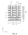
- FIG. 8 is a flow cross-sectional view illustrating a method for manufacturing a nonvolatile semiconductor memory device according to the second embodiment
- FIG. 9 is a flow cross-sectional view illustrating a method for manufacturing a nonvolatile semiconductor memory device according to the second embodiment
- FIG. 10 is a flow cross-sectional view illustrating a method for manufacturing a nonvolatile semiconductor memory device according to the second embodiment
- FIG. 11 is a flow cross-sectional view illustrating a method for manufacturing a nonvolatile semiconductor memory device according to the second embodiment
- FIG. 12 is a flow cross-sectional view illustrating a method for manufacturing a nonvolatile semiconductor memory device according to the second embodiment
- FIG. 13 is a flow cross-sectional view illustrating a method for manufacturing a nonvolatile semiconductor memory device according to the second embodiment
- FIG. 14 is a flow cross-sectional view illustrating a method for manufacturing a nonvolatile semiconductor memory device according to the second embodiment
- FIG. 15 is a flow cross-sectional view illustrating a method for manufacturing a nonvolatile semiconductor memory device according to the second embodiment
- FIG. 16 is a flow cross-sectional view illustrating a method for manufacturing a nonvolatile semiconductor memory device according to the second embodiment.
- FIG. 17 is a schematic cross-sectional view explaining a operation of a nonvolatile semiconductor memory device according to the second embodiment.
- FIG. 1 is a perspective cross-sectional view illustrating a nonvolatile semiconductor memory device according to this embodiment.
- FIG. 2 is a perspective view illustrating the nonvolatile semiconductor memory device according to this embodiment.
- control gate electrodes CG, floating gate electrodes FG, and a semiconductor pillar SP described later are illustrated.
- a nonvolatile semiconductor memory device 1 (hereinafter may be referred to simply as “device 1 ”) according to this embodiment, a plurality of interlayer insulating films ILD and a plurality of control gate electrodes CG are alternately stacked on a substrate (not illustrated) to form a stacked body ML.
- a through-hole H extending in the stacking direction is formed in the stacked body ML.
- the diameter of the through-hole H is larger than the thickness of each of the interlayer insulating films ILD.
- a silicon pillar SP is buried in the through-hole H.
- a portion of the interlayer insulating films ILD adjacent to the through-hole H is removed, and the interlayer insulating films ILD go back away from the through-hole H.
- a removed portion A in which the interlayer insulating films ILD do not exist is formed in a region between the control gate electrodes CG and around the through-hole H.
- a floating gate electrode FG is buried in this removed portion A.
- the floating gate electrode FG having a circular shape is provided between the control gate electrodes CG so as to surround the semiconductor pillar SP.
- the floating gate electrode FG is disposed concentrically with the semiconductor pillar SP.
- an insulating film IPD is provided on the side faces of the through-hole H and the removed portion A.
- the insulating film IPD is provided between the semiconductor pillar SP and the floating gate electrode FG, and the control gate electrodes CG and the interlayer insulating films ILD, and insulates the semiconductor pillar SP and the floating gate electrode FG from the control gate electrodes CG.
- the insulating film IPD is formed thick enough to insulate them from each other.
- an insulating film TOx is provided between the semiconductor pillar SP and the floating gate electrode FG.
- the insulating film TOx has a film thickness that allows an electron to pass therethrough by the tunnel effect when a voltage not less than a certain level is applied between the semiconductor pillar SP and the floating gate electrode FG.
- the electric potentials of the semiconductor pillar SP and the control gate electrodes CG can be each controlled by a peripheral circuit (not illustrated). Thereby, in the device 1 , the electric potentials of the semiconductor pillar SP and the control gate electrodes CG are controlled to transfer an electron between the semiconductor pillar SP and the floating gate electrode FG, and thus a charge can be stored in an optional floating gate electrode FG. Consequently, data can be memorized in the floating gate electrode FG. That is, in the device 1 , a memory cell is configured for each floating gate electrode FG.
- a plurality of through-holes H are arranged in a matrix form in the stacked body ML.
- the semiconductor pillar SP, the floating gate electrodes FG, the insulating film IPD, and the insulating film TOx are provided in and around each of the through-holes H.
- a plurality of memory cells are arranged in a three-dimensional matrix form.
- the semiconductor pillar SP a plurality of the control gate electrodes CG provided around the semiconductor pillar SP, and a plurality of the floating gate electrodes FG provided around the semiconductor pillar SP are provided.
- the semiconductor pillar SP, the control gate electrodes CG, and the floating gate electrode FG are isolated from each other via the interlayer insulating films ILD, the insulating film IPD, and the insulating film TOx.
- the control gate electrodes CG and the floating gate electrodes FG are alternately arranged in the direction in which the semiconductor pillar SP extends.
- the diameter of the semiconductor pillar SP is larger than the thickness of the floating gate electrode FG in the direction in which the semiconductor pillar SP extends.
- the control gate electrodes CG are formed of a conductive material such as polysilicon into which impurities are introduced or a metal.
- the interlayer insulating films ILD, the insulating film IPD, and the insulating film TOx are formed of an insulating material such as silicon oxide.
- the floating gate electrode FG is formed of silicon.
- the semiconductor pillar SP is formed of a semiconductor material such as polysilicon into which impurities are introduced.
- a plurality of interlayer insulating films ILD and a plurality of control gate electrodes CG are alternately stacked on a substrate (not illustrated) to form a stacked body ML.
- a through-hole H extending in the stacking direction of the stacked body ML is formed in the stacked body ML.
- the diameter of the through-hole H is made larger than the thickness of each of the interlayer insulating films ILD.
- a portion of the interlayer insulating films ILD facing the through-hole H is etched via the through-hole H to remove this portion in a circular shape. Thereby, a removed portion A of the interlayer insulating films ILD is formed between control gate electrodes CG.
- an insulating film IPD is formed on the inner faces of the through-hole H and the removed portion A.
- the film thickness of the insulating film IPD is made enough to ensure insulation properties.
- a floating gate electrode FG made of silicon is buried in the removed portion A.
- an insulating film TOx is formed so as to cover a portion of the floating gate electrode FG facing the through-hole H.
- the film thickness of the insulating film TOx is made enough for a tunnel current to flow under certain conditions.
- a semiconductor pillar SP made of, for example, silicon is buried in the through-hole H. Thereby, the nonvolatile semiconductor memory device 1 according to this embodiment is manufactured.
- the electric potentials of one pair of control gate electrodes CG that are disposed on both sides of this floating gate electrode FG are set higher than the electric potential of the semiconductor pillar SP, i.e., a channel.
- the electric potential of the floating gate electrode FG increases due to the coupling effect, and an electron is injected from the semiconductor pillar SP into the floating gate electrode FG via the insulating film TOx by the tunnel effect.
- the injected electron is stored in the floating gate electrode FG.
- data are written in this floating gate electrode FG.
- the electric potential of the semiconductor pillar SP is set higher than the electric potential of the floating gate electrode FG. Thereby, the electron stored in the floating gate electrode FG is extracted into the semiconductor pillar SP by the tunnel effect, and the data are erased.
- the electric potentials of the control gate electrodes CG on both sides of this floating gate electrode FG are set appropriately so that whether or not a current flows in the semiconductor pillar SP may depend on whether or not an electron is stored in the floating gate electrode.
- the electric potentials of other control gate electrodes CG penetrated by the semiconductor pillar SP which penetrates the control gate electrodes CG mentioned above are set appropriately so that a current may flow in the semiconductor pillar SP regardless of whether or not an electron is stored in the other floating gate electrodes FG.
- a voltage is applied to both ends of the semiconductor pillar SP to detect whether or not a current flows in the semiconductor pillar SP. Thereby, the data written in this floating gate electrode FG can be read out.
- a plurality of memory cells are arranged in a three-dimensional matrix form.
- the integration degree of memory cells per unit area can be made high.
- through-holes H are processed collectively in the stacked body ML, an increase in manufacturing cost can be suppressed even if the number of stacked layers increases.
- each memory cell is configured by the floating gate electrode FG, and data are memorized by storing an electron in the floating gate electrode FG.
- the electron stored in the floating gate electrode FG is extracted into the semiconductor pillar SP by the tunnel effect, and thereby the data are erased from the floating gate electrode FG. Since the tunnel current by an electron is larger than the tunnel current by a hole if the applied voltage is the same, the device 1 achieves high erasing speeds.
- the electric potential of the floating gate electrode FG is controlled by controlling the electric potentials of control gate electrodes CG. Since the control gate electrodes CG are disposed on both sides of a floating gate electrode FG, the rate of coupling between the control gate electrodes CG and the floating gate electrode FG is high. Therefore, the driving electric potential has a wide margin. Consequently, the electric potentials of the control gate electrodes CG can be kept low, for example, and this embodiment is suitable for miniaturization.
- the floating gate electrode FG is formed of silicon, which has a narrower band gap than silicon oxide that forms the insulating film IPD and the insulating film TOx. Therefore, the floating gate electrode FG can retain injected electrons stably.
- floating gate electrodes FG are away from each other. Therefore, an electron that has once been stored in the floating gate electrode FG does not move to an adjacent floating gate electrode FG. Thereby, fluctuation in the threshold of a memory cell due to the movement of electrons between memory cells does not occur.
- a memory cell is configured by the floating gate electrode in a nonvolatile semiconductor memory device of three-dimensional stacked type that is manufactured by collective processing.
- the integration rate per unit area can be increased by integrating memory cells three-dimensionally, and the manufacturing cost can be reduced by collective processing.
- electrons are stored in a silicon nitride film that is continuously formed on the inner face of a through-hole, there is a problem that the erasing speed is slow and interference between memory cells easily occurs.
- the threshold of the MONOS type transistor that forms a memory cell may fluctuate.
- FIG. 3 is a perspective view illustrating a nonvolatile semiconductor memory device according to this embodiment.
- FIG. 4 is a cross-sectional view illustrating a nonvolatile semiconductor memory device according to this embodiment.
- FIG. 3 for convenience of illustration, only a part of the conductive portions and the semiconductor portions is illustrated and the insulating portions are omitted.
- This embodiment is an embodiment that embodies the first embodiment described above in an aspect closer to the actual devices. Effects of this embodiment are like the first embodiment described above.
- a silicon substrate 11 made of, for example, single-crystal silicon is provided.
- An insulating film 12 made of, for example, silicon oxide is provided on the silicon substrate 11 , and a conductive film PG made of, for example, polysilicon is provided thereon.
- Concaves 13 are provided at the top face of the conductive film PG, and a connection member 14 made of, for example, polysilicon having N-type conductivity is buried in the concave 13 .
- a plurality of interlayer insulating films ILD and a plurality of control gate electrodes CG are alternately stacked layer by layer on the conductive film PG, and thereby a stacked body ML is formed.
- the configuration of the stacked body ML is like the first embodiment described above. That is, a plurality of through-holes H are formed in the stacked body ML in a matrix form as viewed from the stacking direction, and a semiconductor pillar SP made of polysilicon having N-type conductivity is buried in each of the through-holes H.
- the diameter of the through-hole H is larger than the thickness of each of the interlayer insulating films ILD.
- a portion of the interlayer insulating films ILD around the through-hole H goes back to form a removed portion A of the interlayer insulating films ILD.
- a floating gate electrode FG is buried in the removed portion A.
- the floating gate electrode FG is formed of polysilicon having N + -type conductivity, and has a circular shape surrounding the semiconductor pillar SP. Further, the semiconductor pillar SP and the floating gate electrode FG are insulated from the control gate electrodes CG by an insulating film IPD, and an insulating film TOx is provided between the floating gate electrode FG and the semiconductor pillar SP.
- the insulating film TOx is provided also on the inner face of the concave 13 of the conductive film PG and insulates the connection member 14 from the conductive film PG.
- an XYZ orthogonal coordinate system is used in this embodiment.
- this coordinate system two directions parallel to the top face of the silicon substrate 11 and orthogonal to each other are defined as an X direction and a Y direction, and the direction orthogonal to both the X direction and the Y direction, that is, the stacking direction of the layers described above is defined as a Z direction.
- connection member 14 has a shape of rectangular parallelepiped extending in the X direction.
- the top faces of both ends of the connection member 14 are each connected to the lower end of the semiconductor pillar SP.
- two semiconductor pillars SP that are adjacent to each other in the X direction are connected to each other via the connection member 14 .
- An insulating film 16 made of, for example, silicon oxide is provided on the stacked body ML, and thereon selection gate electrodes SG made of a conductive material such as polysilicon into which impurities are introduced are provided.
- An insulating film 17 made of, for example, silicon oxide and an insulating film 18 made of, for example, silicon oxide are provided on the selection gate electrodes SG.
- An upper gate stacked body 20 is configured by the insulating film 16 , the selection gate electrodes SG, the insulating film 17 , and the insulating film 18 .
- Through-holes 21 extending in the Z direction (stacking direction) are formed in this upper gate stacked body 20 .
- the through-holes 21 are formed immediately above the through-holes H and communicate with the through-holes H.
- a gate insulating film 22 made of, for example, silicon oxide is formed on the side face of the through-hole 21 .
- Polysilicon into which impurities are introduced for example, is buried in the lower portion of the through-hole 21 , that is, the portion surrounded by the insulating film 16 , the selection gate electrode SG, and the lower portion of the insulating film 17 , and this forms a semiconductor pillar 23 .
- a metal material is buried in the upper portion of the through-hole 21 , that is, the portion surrounded by the insulating film 18 and the upper portion of the insulating film 17 , and this forms a plug 24 .
- the semiconductor pillar SP, the semiconductor pillar 23 , and the plug 24 that are arranged in the Z direction are connected to each other.
- Slits 26 extending in the Y direction are formed from above in the stacked body ML and the upper gate stacked body 20 .
- the slits 26 are formed in regions between through-holes that are arranged in the X direction, and divide the lowermost control gate electrode CG but do not divide the connection member 14 .
- An insulating member 27 made of, for example, silicon oxide is buried in the slit 26 .
- the control gate electrodes CG and the selection gate electrodes SG are divided along the X direction to be shaped into stripes extending in the Y direction.
- Each control gate electrode CG and each selection gate electrode SG correspond to each column of semiconductor pillars SP and 23 that are arranged along the Y direction.
- a source line SL made of, for example, a metal is formed on the upper gate stacked body 20 .
- the source line SL has a stripe shape extending in the Y direction, and has a width greater than the widths of the control gate electrode CG and the selection gate electrode SG.
- the source line SL is connected to semiconductor pillars 23 that are arranged in two columns extending along the Y direction, via plugs 24 .
- Each of the two columns of semiconductor pillars that are connected to one source line SL is connected to a mutually-different connection member 14 .
- one column of semiconductor pillars out of the two columns of semiconductor pillars that are connected to one connection member 14 is connected to a common source line SL, and the other column of semiconductor pillars is not connected to any source lines SL.
- An insulating film 28 made of, for example, silicon oxide is provided on the upper gate stacked body 20 so as to bury the source line SL.
- a plug 29 is buried immediately above the semiconductor pillar that is not connected to the source line SL.
- Bit lines BL extending in the X direction are formed on the insulating film 28 and are connected to plugs 29 .
- a U-shaped pillar 25 that is composed of the plug 29 , the plug 24 , the semiconductor pillar 23 , the semiconductor pillar SP, the connection member 14 , the semiconductor pillar SP, the semiconductor pillar 23 , and the plug 24 is formed between the bit line BL and the source line SL.
- the connection member 14 and one pair of semiconductor pillars SP connected thereto are integrally formed.
- FIGS. 5 to 16 are process cross-sectional views illustrating a method for manufacturing the nonvolatile semiconductor memory device according to this embodiment.
- an insulating film 12 made of, for example, silicon oxide is formed on a silicon substrate 11 made of, for example, single-crystal silicon.
- Amorphous silicon into which phosphorus (P), for example, is introduced is deposited thereon to form a conductive film PG.
- concaves 13 having a strip shape extending in the X direction are formed on the top face of the conductive film PG, and a sacrifice member 31 made of silicon nitride is buried in each of the concaves 13 .
- interlayer insulating films ILD made of silicon oxide and control gate electrodes CG made of amorphous silicon into which phosphorus is introduced are alternately stacked on the conductive film PG to form a stacked body ML.
- a silicon oxide film 32 is formed on the stacked body ML.
- etching is performed from above on the silicon oxide film 32 and the stacked body ML to form through-holes H extending in the Z direction in the stacked body ML, so that the through-holes H may reach both ends of the sacrifice member 31 .
- the through-holes H are formed in a matrix form as viewed from the Z direction.
- the diameter of the through-hole H is made larger than the thickness of each of the interlayer insulating films ILD.
- silicon oxide is thinly deposited over the entire surface by, for example, LPCVD (low pressure chemical vapor deposition).
- LPCVD low pressure chemical vapor deposition
- an insulating film IPD made of silicon oxide is formed over the entire exposed surface.
- the insulating film IPD is formed on the inner faces of the through-hole H and the removed portion A, and is formed also on the top face of the stacked body ML and on the top face of the sacrifice member 31 .
- amorphous silicon having N + -type conductivity is thinly deposited by, for example, LPCVD to form a silicon layer 33 over the entire exposed surface.
- the amorphous silicon is deposited in an appropriate amount so that the removed portion A of the interlayer insulating films ILD may be completely filled up with the silicon layer 33 , but the inside of the through-hole H may not be completely filled up with the silicon layer 33 . Since the diameter of the through-hole H is larger than the thickness of the interlayer insulating films ILD, that is, the height of the removed portion A, such setting of the deposition amount is possible.
- anisotropic etching such as RIE (reactive ion etching) is performed to remove the silicon layer 33 deposited on the bottom face of the through-hole H. At this time, the silicon layer 33 deposited on the top face of the stacked body ML also is removed.
- RIE reactive ion etching
- RIE is performed over the entire surface to remove the insulating film IPD from the bottom face of the through-hole H. At this time, the insulating film IPD deposited on the top face of the stacked body ML also is removed.
- wet etching using hot phosphoric acid is performed to remove the sacrifice member 31 (see FIG. 10 ) from the concave 13 via the through-hole H.
- isotropic etching such as CDE (chemical dry etching) is performed to remove the silicon layer 33 from the side face of the through-hole H.
- CDE chemical dry etching
- a silicon oxide film is thinly deposited by LPCVD, for example.
- an insulating film TOx is formed on a face of the floating gate electrode FG exposed to the through-hole H, on the inner face of the concave 13 , and on the insulating film IPD.
- the insulating film TOx may be formed by thermal oxidation treatment. In this case, the insulating film TOx is not formed on the insulating film IPD.
- amorphous silicon having N-type conductivity is deposited over the entire surface to fill up the through-hole H and the concave 13 .
- a connection member 14 is formed in the concave 13
- a semiconductor pillar SP is formed in the through-hole H.
- one connection member 14 and two semiconductor pillars SP that are connected to both ends of the connection member 14 are integrally formed.
- the amorphous silicon is removed from the top face of the stacked body ML.
- silicon oxide is deposited on the stacked body ML to form an insulating film 16 ; amorphous silicon into which impurities are introduced is deposited to form a selection gate electrode SG; and silicon oxide is deposited to form an insulating film 17 .
- through-holes 21 are formed in regions that are located in the insulating film 16 , the selection gate electrode SG, and the insulating film 17 , and immediately above the through-holes H by etching such as RIE.
- a dielectric material such as silicon oxide is deposited over the entire surface to form a gate insulating film 22 on the side face of the through-hole 21 and to form an insulating film 18 on the dielectric film 17 .
- anisotropic etching such as RIE is performed to remove the gate insulating film 22 from the bottom face of the through-hole 21 .
- amorphous silicon is buried in the lower portion of the through-hole 21 , that is, the portion surrounded by the insulating film 16 , the selection gate electrode SG, and the lower portion of the insulating film 17 to form a semiconductor pillar 23
- a slit 26 extending in the Y direction is formed in the upper gate stacked body 20 and the stacked body ML.
- the slit 26 is formed between semiconductor pillars that are arranged along the X direction, with an appropriate depth so that the lowermost control gate electrode CG may be divided but the connection member 14 may not be divided.
- the selection gate electrode SG and the control gate electrodes CG are divided along the X direction for each semiconductor pillar, and are shaped into stripes extending in the Y direction.
- silicon oxide is buried in the slit 26 to form an insulating member 27 .
- a silicide may be formed on the side face of the control gate electrodes CG exposed to the slit 26 .
- a metal is deposited over the entire surface and patterned.
- a plug 24 is buried in the upper portion of the through-hole 21 , that is, on the semiconductor pillar 23 , and a source line SL extending in the Y direction is formed on the insulating film 18 and the plug 24 .
- the source line SL is connected to one of the two semiconductor pillars that are connected to each connection member 14 . Then, silicon oxide is deposited so as to bury the source line SL to form an insulating film 28 . Next, through-holes are formed in the insulating film 28 , and plugs 29 made of a metal are buried.
- bit line BL extending in the X direction is formed on the insulating film 28 .
- the bit line BL is connected to a semiconductor pillar that is not connected to the source line SL, out of two semiconductor pillars that are connected to each connection member 14 , via the plug 29 .
- the amorphous silicon deposited at each portion becomes polysilicon by the heat treatments accompanying the processes so far, and thus the impurities are activated.
- the nonvolatile semiconductor memory device 2 is manufactured.
- FIG. 17 is a schematic cross-sectional view describing the operation of the nonvolatile semiconductor memory device according to this embodiment.
- control gate electrodes CG through which one U-shaped pillar 25 penetrates are marked with the signs “CG 1 ” to “CG 10 ” from a bit line BL side to a source line SL side.
- floating gate electrodes FG through which the one U-shaped pillar 25 penetrates are marked with the signs “FG 1 ” to “FG 10 ” from the bit line BL side to the source line SL side.
- the selection gate electrode on the bit line BL side is marked with the sign “SGb”, and the selection gate electrode on the source line SL side is marked with the sign “SGs.”
- the electric potential of the selection gate electrode SGb through which the selected pillar penetrates is set to the power source potential Vdd (for example, 3 V).
- the electric potential of the bit line BL to which the selected pillar is connected is set to the grounding potential GND (0 V).
- the selection transistor on the bit line side that is formed at the intersection of the selection gate electrode SGb and the selected pillar becomes in the ON state.
- the electric potentials of the other bit lines BL are set to the power source potential Vdd (for example, 3 V).
- the selection transistors of the other U-shaped pillars 25 on the bit line side become in the OFF state.
- the electric potential of the selection gate electrode SGs that belongs to the selected pillar is set to the grounding potential GND (0 V), and the electric potential of the source line SL that is connected to the selected pillar is set to the power source potential Vdd (for example, 3 V).
- Vdd for example, 3 V
- the selection transistor on the source line side that is formed at the intersection of the selection gate electrode SGs and the selected pillar becomes in the OFF state. Consequently, the selected pillar is connected to the bit line BL and is cut off from the source line SL.
- the electric potentials of the control gate electrodes CG 2 and CG 3 that are located on both sides of the floating gate electrode FG 2 are raised to an electric potential Vpgm (for example, 20 V).
- Vpgm for example, 20 V
- the electric potential of the floating gate electrode FG 2 rises due to the coupling with the control gate electrodes CG 2 and CG 3 to become an electric potential close to the electric potential Vpgm (for example, 20 V).
- the electric potentials of the control gate electrodes CG other than the control gate electrodes CG 2 and CG 3 and the conductive film PG are set to an electric potential Vpass (for example, 10 V).
- the electric potentials of other floating gate electrodes FG 4 to FG 10 through which the selected pillar penetrates become an electric potential close to the electric potential Vpass (for example, 10 V), because the electric potentials of the control gate electrodes CG on both sides thereof and the conductive film PG are set to the electric potential Vpass (for example, 10 V) and the coupling with them raises the voltage.
- the electric potential of one of the control gate electrodes on both sides is set to the electric potential Vpgm (for example, 20 V) and the electric potential of the other is set to the electric potential Vpass (for example, 10 V).
- the electric potentials of the floating gate electrodes FG 1 and FG 3 become an electric potential between the electric potential of the floating gate electrode FG 2 and the electric potentials of the floating gate electrodes FG 4 to FG 10 .
- the electric potentials of all the control gate electrodes CG and the conductive film PG are set to the grounding potential GND (0 V). Thereby, the electric potentials of all the floating gate electrodes FG become an electric potential close to the grounding potential GND (0 V), by the coupling with the control gate electrodes CG and the conductive film PG.
- the electric potential of the bit line BL (or the bit line BL and the source line SL) is raised to an electric potential Vera (for example, 20 V).
- Vera for example, 20 V
- the electric potential of the selection gate electrode SGb (or the selection gate electrodes SGb and SGs) is raised to an electric potential VeraG.
- GIDL gate induced drain leakage
- the electric potentials of the floating gate electrodes FG are close to the grounding potential GND (0 V). Therefore, when the electric potential of the U-shaped pillar 25 rises, a high voltage is applied between the U-shaped pillar 25 and the floating gate electrodes FG, and electrons stored in floating gate electrodes FG are extracted into the U-shaped pillar 25 via the insulating film TOx. Thereby, the data written in all the floating gate electrodes FG are collectively erased.
- the electric potential of the bit line BL that is connected to the selected pillar is set to an electric potential VBL (for example, 1 V), and the electric potentials of all the source lines SL are set to the grounding potential GND (0 V).
- the electric potentials of the selection gate electrodes SGb and SGs through which the selected pillar penetrates are set to the power source potential Vdd (for example, 3 V).
- the electric potentials of the control gate electrodes CG other than the control gate electrodes CG 2 and CG 3 , and the electric potential of the conductive film PG are set to an electric potential Vread (for example, 5 V).
- the electric potential Vread is appropriately selected so that all the transistors formed at the intersections of the selected pillar and the control gate electrodes CG may become in the ON state, and also all the transistors formed at the intersections of the selected pillar and the floating gate electrodes FG other than the floating gate electrode FG 2 may become in the ON state due to a rise in the electric potentials of the floating gate electrodes FG, which is caused by the coupling with the control gate electrodes CG.
- the electric potentials of the control gate electrodes CG 2 and CG 3 that are disposed on both sides of the floating gate electrode FG 2 are set to the grounding potential GND (0 V) or an electric potential between the grounding potential GND (0 V) and the electric potential Vread (for example, 5 V).
- This electric potential is appropriately selected so that the transistor formed at the intersection of the selected pillar and the floating gate electrode FG 2 may become in the OFF state when an electron is stored in the floating gate electrode FG 2 , and this transistor may become in the ON state when an electron is not stored in the floating gate electrode FG 2 .
- the threshold of the transistor formed at the intersection of the selected pillar and the floating gate electrode FG 2 depends on whether or not an electron is stored in the floating gate electrode FG 2 , and the electric potentials of the control gate electrodes CG 2 and CG 3 are set so that the conduction state of this transistor may depend on this threshold.
- portions of the selected pillar surrounded by the selection gate electrodes SGb and SGs, all the control gate electrodes CG, and the floating gate electrodes FG other than the floating gate electrode FG 2 become constantly in the ON state, and the portion surrounded by the floating gate electrode FG 2 varies in conduction state with whether or not a charge is stored in the floating gate electrode FG 2 . That is, when an electron is stored in the floating gate electrode FG 2 , then a current does not flow from the bit line BL to the source line SL, and when an electron is not stored in the floating gate electrode FG 2 , then a current flows from the bit line BL to the source line SL via the selected pillar. Therefore, by measuring this current, the data written in the floating gate electrode FG 2 can be read out.
Landscapes
- Engineering & Computer Science (AREA)
- Microelectronics & Electronic Packaging (AREA)
- Power Engineering (AREA)
- Physics & Mathematics (AREA)
- Condensed Matter Physics & Semiconductors (AREA)
- General Physics & Mathematics (AREA)
- Computer Hardware Design (AREA)
- Ceramic Engineering (AREA)
- Manufacturing & Machinery (AREA)
- Non-Volatile Memory (AREA)
- Read Only Memory (AREA)
- Semiconductor Memories (AREA)
Priority Applications (1)
| Application Number | Priority Date | Filing Date | Title |
|---|---|---|---|
| US13/864,882 US9029934B2 (en) | 2009-01-22 | 2013-04-17 | Nonvolatile semiconductor memory device including floating gate electrodes formed between control gate electrodes and vertically formed along a semiconductor pillar |
Applications Claiming Priority (2)
| Application Number | Priority Date | Filing Date | Title |
|---|---|---|---|
| JP2009-012052 | 2009-01-22 | ||
| JP2009012052A JP5388600B2 (ja) | 2009-01-22 | 2009-01-22 | 不揮発性半導体記憶装置の製造方法 |
Related Child Applications (1)
| Application Number | Title | Priority Date | Filing Date |
|---|---|---|---|
| US13/864,882 Division US9029934B2 (en) | 2009-01-22 | 2013-04-17 | Nonvolatile semiconductor memory device including floating gate electrodes formed between control gate electrodes and vertically formed along a semiconductor pillar |
Publications (2)
| Publication Number | Publication Date |
|---|---|
| US20100181612A1 US20100181612A1 (en) | 2010-07-22 |
| US8440528B2 true US8440528B2 (en) | 2013-05-14 |
Family
ID=42336229
Family Applications (2)
| Application Number | Title | Priority Date | Filing Date |
|---|---|---|---|
| US12/638,480 Active 2031-03-05 US8440528B2 (en) | 2009-01-22 | 2009-12-15 | Method for manufacturing a vertical nonvolatile semiconductor memory device including forming floating gates within the recesses created on the interlayer insulating films |
| US13/864,882 Active 2030-02-10 US9029934B2 (en) | 2009-01-22 | 2013-04-17 | Nonvolatile semiconductor memory device including floating gate electrodes formed between control gate electrodes and vertically formed along a semiconductor pillar |
Family Applications After (1)
| Application Number | Title | Priority Date | Filing Date |
|---|---|---|---|
| US13/864,882 Active 2030-02-10 US9029934B2 (en) | 2009-01-22 | 2013-04-17 | Nonvolatile semiconductor memory device including floating gate electrodes formed between control gate electrodes and vertically formed along a semiconductor pillar |
Country Status (3)
| Country | Link |
|---|---|
| US (2) | US8440528B2 (ko) |
| JP (1) | JP5388600B2 (ko) |
| KR (1) | KR20100086435A (ko) |
Cited By (5)
| Publication number | Priority date | Publication date | Assignee | Title |
|---|---|---|---|---|
| US20120092926A1 (en) * | 2010-10-13 | 2012-04-19 | Sung Jin Whang | Three dimensional non-volatile memory device and method of manufacturing the same |
| CN106024790A (zh) * | 2015-03-25 | 2016-10-12 | 爱思开海力士有限公司 | 半导体器件及制造其的方法 |
| US9666592B2 (en) | 2014-09-29 | 2017-05-30 | Samsung Electronics Co., Ltd. | Memory devices and methods of fabricating the same |
| US20170271021A1 (en) * | 2016-03-15 | 2017-09-21 | Kabushiki Kaisha Toshiba | Memory device |
| US10680011B2 (en) * | 2018-06-22 | 2020-06-09 | Samsung Electronics Co., Ltd. | Vertical semiconductor devices |
Families Citing this family (71)
| Publication number | Priority date | Publication date | Assignee | Title |
|---|---|---|---|---|
| JP5388537B2 (ja) * | 2008-10-20 | 2014-01-15 | 株式会社東芝 | 不揮発性半導体記憶装置、及びその製造方法 |
| JP5317664B2 (ja) * | 2008-12-17 | 2013-10-16 | 株式会社東芝 | 不揮発性半導体記憶装置の製造方法 |
| KR101539699B1 (ko) | 2009-03-19 | 2015-07-27 | 삼성전자주식회사 | 3차원 구조의 비휘발성 메모리 소자 및 그 제조방법 |
| JP5380190B2 (ja) * | 2009-07-21 | 2014-01-08 | 株式会社東芝 | 不揮発性半導体記憶装置及びその製造方法 |
| KR101549858B1 (ko) * | 2009-07-31 | 2015-09-03 | 삼성전자주식회사 | 수직 채널 구조의 플래쉬 메모리 소자 |
| JP2011040421A (ja) * | 2009-08-06 | 2011-02-24 | Elpida Memory Inc | 半導体装置およびその製造方法 |
| KR101045073B1 (ko) * | 2009-08-07 | 2011-06-29 | 주식회사 하이닉스반도체 | 수직채널형 비휘발성 메모리 소자 및 그 제조 방법 |
| JP4975794B2 (ja) * | 2009-09-16 | 2012-07-11 | 株式会社東芝 | 不揮発性半導体記憶装置 |
| JP5121869B2 (ja) | 2010-03-23 | 2013-01-16 | 株式会社東芝 | 不揮発性半導体記憶装置の製造方法 |
| US9000509B2 (en) | 2010-05-31 | 2015-04-07 | Hynix Semiconductor Inc. | Three dimensional pipe gate nonvolatile memory device |
| KR101083637B1 (ko) * | 2010-05-31 | 2011-11-16 | 주식회사 하이닉스반도체 | 비휘발성 메모리 장치 및 그 제조 방법 |
| US8803214B2 (en) | 2010-06-28 | 2014-08-12 | Micron Technology, Inc. | Three dimensional memory and methods of forming the same |
| KR20120006843A (ko) * | 2010-07-13 | 2012-01-19 | 삼성전자주식회사 | 반도체 장치 및 그 제조 방법 |
| JP2012069205A (ja) * | 2010-09-22 | 2012-04-05 | Toshiba Corp | 不揮発性半導体記憶装置 |
| JP2012119445A (ja) | 2010-11-30 | 2012-06-21 | Toshiba Corp | 半導体記憶装置および半導体記憶装置の製造方法 |
| KR20120066331A (ko) * | 2010-12-14 | 2012-06-22 | 에스케이하이닉스 주식회사 | 3차원 구조의 비휘발성 메모리 소자 및 그 제조 방법 |
| KR101825534B1 (ko) | 2011-02-07 | 2018-02-06 | 삼성전자주식회사 | 3차원 반도체 장치 |
| US8759895B2 (en) * | 2011-02-25 | 2014-06-24 | Micron Technology, Inc. | Semiconductor charge storage apparatus and methods |
| JP2012204430A (ja) * | 2011-03-24 | 2012-10-22 | Toshiba Corp | 不揮発性半導体記憶装置及びその製造方法 |
| KR101842237B1 (ko) | 2011-04-19 | 2018-03-27 | 삼성전자주식회사 | 3차원 반도체 메모리 소자 및 이를 제조하는 방법 |
| JP2012227326A (ja) * | 2011-04-19 | 2012-11-15 | Toshiba Corp | 不揮発性半導体記憶装置とその製造方法 |
| US8860117B2 (en) | 2011-04-28 | 2014-10-14 | Micron Technology, Inc. | Semiconductor apparatus with multiple tiers of memory cells with peripheral transistors, and methods |
| KR101933665B1 (ko) * | 2011-05-19 | 2018-12-31 | 삼성전자주식회사 | 3차원 반도체 메모리 장치의 제조 방법 |
| JP2013069932A (ja) | 2011-09-22 | 2013-04-18 | Toshiba Corp | 不揮発性半導体記憶装置及びその製造方法 |
| KR101857025B1 (ko) | 2011-10-31 | 2018-05-14 | 삼성전자주식회사 | 반도체 소자의 제조방법 |
| US8837223B2 (en) | 2011-11-21 | 2014-09-16 | Kabushiki Kaisha Toshiba | Nonvolatile semiconductor memory device and method for manufacuring the same |
| KR101942421B1 (ko) * | 2011-12-29 | 2019-01-30 | 에스케이하이닉스 주식회사 | 비휘발성 메모리 장치 및 그 제조 방법 |
| JP5808708B2 (ja) * | 2012-04-10 | 2015-11-10 | 株式会社東芝 | 不揮発性半導体記憶装置及びその製造方法 |
| US8964474B2 (en) | 2012-06-15 | 2015-02-24 | Micron Technology, Inc. | Architecture for 3-D NAND memory |
| TWI488265B (zh) * | 2012-07-11 | 2015-06-11 | Powerchip Technology Corp | 立體垂直式記憶體的製作方法 |
| US9076824B2 (en) | 2012-11-02 | 2015-07-07 | Micron Technology, Inc. | Memory arrays with a memory cell adjacent to a smaller size of a pillar having a greater channel length than a memory cell adjacent to a larger size of the pillar and methods |
| US8791578B2 (en) * | 2012-11-12 | 2014-07-29 | Hong Kong Applied Science and Technology Research Institute Company Limited | Through-silicon via structure with patterned surface, patterned sidewall and local isolation |
| US8946807B2 (en) | 2013-01-24 | 2015-02-03 | Micron Technology, Inc. | 3D memory |
| US9064970B2 (en) | 2013-03-15 | 2015-06-23 | Micron Technology, Inc. | Memory including blocking dielectric in etch stop tier |
| US9276011B2 (en) | 2013-03-15 | 2016-03-01 | Micron Technology, Inc. | Cell pillar structures and integrated flows |
| US9184175B2 (en) | 2013-03-15 | 2015-11-10 | Micron Technology, Inc. | Floating gate memory cells in vertical memory |
| JP2014187321A (ja) * | 2013-03-25 | 2014-10-02 | Toshiba Corp | 不揮発性半導体記憶装置およびその製造方法 |
| KR20140117212A (ko) * | 2013-03-26 | 2014-10-07 | 에스케이하이닉스 주식회사 | 반도체 장치 |
| US9437604B2 (en) | 2013-11-01 | 2016-09-06 | Micron Technology, Inc. | Methods and apparatuses having strings of memory cells including a metal source |
| US9136278B2 (en) * | 2013-11-18 | 2015-09-15 | Micron Technology, Inc. | Methods of forming vertically-stacked memory cells |
| US9478643B2 (en) | 2013-12-24 | 2016-10-25 | Intel Corporation | Memory structure with self-aligned floating and control gates and associated methods |
| JP5676787B1 (ja) * | 2014-01-16 | 2015-02-25 | ユニサンティス エレクトロニクス シンガポール プライベート リミテッドUnisantis Electronics Singapore Pte Ltd. | 半導体装置 |
| US9252148B2 (en) | 2014-01-22 | 2016-02-02 | Micron Technology, Inc. | Methods and apparatuses with vertical strings of memory cells and support circuitry |
| US9673209B2 (en) | 2014-05-16 | 2017-06-06 | Taiwan Semiconductor Manufacturing Company, Ltd. | Memory device and method for fabricating the same |
| US9595531B2 (en) | 2014-07-11 | 2017-03-14 | Intel Corporation | Aluminum oxide landing layer for conductive channels for a three dimensional circuit device |
| KR20160013765A (ko) * | 2014-07-28 | 2016-02-05 | 삼성전자주식회사 | 반도체 장치 |
| US9263459B1 (en) | 2014-09-26 | 2016-02-16 | Intel Corporation | Capping poly channel pillars in stacked circuits |
| US9893076B2 (en) * | 2015-02-05 | 2018-02-13 | Conversant Intellectual Property Management Inc. | Access transistor of a nonvolatile memory device and method for fabricating same |
| US9893079B2 (en) * | 2015-03-27 | 2018-02-13 | Toshiba Memory Corporation | Semiconductor memory device |
| US9608000B2 (en) | 2015-05-27 | 2017-03-28 | Micron Technology, Inc. | Devices and methods including an etch stop protection material |
| US9324789B1 (en) * | 2015-05-27 | 2016-04-26 | Macronix International Co., Ltd. | Memory device and method for fabricating the same |
| JP2017054941A (ja) * | 2015-09-10 | 2017-03-16 | 株式会社東芝 | 半導体装置及びその製造方法 |
| US9947683B2 (en) * | 2015-09-11 | 2018-04-17 | Toshiba Memory Corporation | Three-dimensional semiconductor memory device and method for manufacturing the same |
| US20170141123A1 (en) * | 2015-11-17 | 2017-05-18 | Kabushiki Kaisha Toshiba | Semiconductor memory device and method for manufacturing same |
| US9679912B1 (en) * | 2015-12-03 | 2017-06-13 | Kabushiki Kaisha Toshiba | Semiconductor device |
| TWI582964B (zh) * | 2015-12-30 | 2017-05-11 | 旺宏電子股份有限公司 | 記憶體元件及其製作方法 |
| US9679650B1 (en) | 2016-05-06 | 2017-06-13 | Micron Technology, Inc. | 3D NAND memory Z-decoder |
| US9748265B1 (en) | 2016-06-07 | 2017-08-29 | Micron Technology, Inc. | Integrated structures comprising charge-storage regions along outer portions of vertically-extending channel material |
| US10283520B2 (en) | 2016-07-12 | 2019-05-07 | Micron Technology, Inc. | Elevationally-extending string of memory cells individually comprising a programmable charge storage transistor and method of forming an elevationally-extending string of memory cells individually comprising a programmable charge storage transistor |
| US10090318B2 (en) | 2016-08-05 | 2018-10-02 | Micron Technology, Inc. | Vertical string of memory cells individually comprising a programmable charge storage transistor comprising a control gate and a charge storage structure and method of forming a vertical string of memory cells individually comprising a programmable charge storage transistor comprising a control gate and a charge storage structure |
| TWI652804B (zh) * | 2016-09-15 | 2019-03-01 | 東芝記憶體股份有限公司 | Semiconductor memory device |
| US11682667B2 (en) * | 2017-06-27 | 2023-06-20 | Semiconductor Energy Laboratory Co., Ltd. | Memory cell including cell transistor including control gate and charge accumulation layer |
| US10553708B2 (en) | 2017-08-29 | 2020-02-04 | International Business Machines Corporation | Twin gate tunnel field-effect transistor (FET) |
| US10729012B2 (en) * | 2018-04-24 | 2020-07-28 | Micron Technology, Inc. | Buried lines and related fabrication techniques |
| US10825867B2 (en) | 2018-04-24 | 2020-11-03 | Micron Technology, Inc. | Cross-point memory array and related fabrication techniques |
| US10950663B2 (en) | 2018-04-24 | 2021-03-16 | Micron Technology, Inc. | Cross-point memory array and related fabrication techniques |
| US10916560B2 (en) | 2019-01-14 | 2021-02-09 | Macronix International Co., Ltd. | Crenellated charge storage structures for 3D NAND |
| CN110098192B (zh) * | 2019-05-23 | 2020-06-30 | 长江存储科技有限责任公司 | 三维存储器及其制备方法 |
| JP2021034486A (ja) * | 2019-08-21 | 2021-03-01 | キオクシア株式会社 | 半導体記憶装置 |
| US11450381B2 (en) | 2019-08-21 | 2022-09-20 | Micron Technology, Inc. | Multi-deck memory device including buffer circuitry under array |
| JP7536625B2 (ja) * | 2020-12-04 | 2024-08-20 | 株式会社東芝 | 半導体装置およびその製造方法 |
Citations (12)
| Publication number | Priority date | Publication date | Assignee | Title |
|---|---|---|---|---|
| US20040079988A1 (en) | 2002-10-28 | 2004-04-29 | Sandisk Corporation | Flash memory cell arrays having dual control gates per memory cell charge storage element |
| KR20050029693A (ko) | 2003-09-22 | 2005-03-28 | 가부시끼가이샤 도시바 | 불휘발성 반도체 기억 장치 |
| US20060060911A1 (en) | 2004-09-21 | 2006-03-23 | Makoto Sakuma | Nonvolatile semiconductor memory device having adjacent selection transistors connected together |
| KR20070096972A (ko) | 2006-03-27 | 2007-10-02 | 가부시끼가이샤 도시바 | 비휘발성 반도체 메모리 장치 및 그의 제조 방법 |
| KR20080092290A (ko) | 2007-04-11 | 2008-10-15 | 가부시끼가이샤 도시바 | 반도체 기억 장치 |
| US20090146206A1 (en) * | 2007-11-30 | 2009-06-11 | Kabushiki Kaisha Toshiba | Non-volatile semiconductor storage device and method of manufacturing the same |
| WO2009075370A1 (en) | 2007-12-11 | 2009-06-18 | Kabushiki Kaisha Toshiba | Non-volatile semiconductor storage device and method of manufacturing the same |
| US20090230458A1 (en) * | 2008-03-14 | 2009-09-17 | Kabushiki Kaisha Toshiba | Non-volatile semiconductor storage device and method of manufacturing the same |
| US20100001247A1 (en) * | 2009-09-18 | 2010-01-07 | Luis Jaimes | Barrier Post and System |
| US20110084331A1 (en) * | 2008-06-03 | 2011-04-14 | Kabushiki Kaisha Toshiba | Semiconductor device |
| US7969789B2 (en) * | 2008-08-06 | 2011-06-28 | Kabushiki Kaisha Toshiba | Method for driving nonvolatile semiconductor memory device |
| US20120028450A1 (en) * | 2008-02-29 | 2012-02-02 | Samsung Electronics Co., Ltd. | Vertical-type semiconductor devices and methods of manufacturing the same |
Family Cites Families (7)
| Publication number | Priority date | Publication date | Assignee | Title |
|---|---|---|---|---|
| JP3651689B2 (ja) * | 1993-05-28 | 2005-05-25 | 株式会社東芝 | Nand型不揮発性半導体記憶装置及びその製造方法 |
| WO2006132158A1 (ja) * | 2005-06-10 | 2006-12-14 | Sharp Kabushiki Kaisha | 不揮発性半導体記憶装置およびその製造方法 |
| JP4791868B2 (ja) * | 2006-03-28 | 2011-10-12 | 株式会社東芝 | Fin−NAND型フラッシュメモリ |
| KR101045073B1 (ko) * | 2009-08-07 | 2011-06-29 | 주식회사 하이닉스반도체 | 수직채널형 비휘발성 메모리 소자 및 그 제조 방법 |
| US8823072B2 (en) * | 2010-04-15 | 2014-09-02 | Samsung Electronics Co., Ltd. | Floating gate type nonvolatile memory device and related methods of manufacture and operation |
| KR101094523B1 (ko) * | 2010-10-13 | 2011-12-19 | 주식회사 하이닉스반도체 | 3차원 구조의 비휘발성 메모리 소자 및 그 제조 방법 |
| US8711630B2 (en) * | 2010-12-29 | 2014-04-29 | Hynix Semiconductor Inc. | Programming method of non-volatile memory device |
-
2009
- 2009-01-22 JP JP2009012052A patent/JP5388600B2/ja active Active
- 2009-12-15 US US12/638,480 patent/US8440528B2/en active Active
-
2010
- 2010-01-21 KR KR1020100005621A patent/KR20100086435A/ko not_active Application Discontinuation
-
2013
- 2013-04-17 US US13/864,882 patent/US9029934B2/en active Active
Patent Citations (15)
| Publication number | Priority date | Publication date | Assignee | Title |
|---|---|---|---|---|
| US20040079988A1 (en) | 2002-10-28 | 2004-04-29 | Sandisk Corporation | Flash memory cell arrays having dual control gates per memory cell charge storage element |
| KR20050029693A (ko) | 2003-09-22 | 2005-03-28 | 가부시끼가이샤 도시바 | 불휘발성 반도체 기억 장치 |
| US7026684B2 (en) | 2003-09-22 | 2006-04-11 | Kabushiki Kaisha Toshiba | Nonvolatile semiconductor memory device |
| US20060060911A1 (en) | 2004-09-21 | 2006-03-23 | Makoto Sakuma | Nonvolatile semiconductor memory device having adjacent selection transistors connected together |
| US20070252201A1 (en) | 2006-03-27 | 2007-11-01 | Masaru Kito | Nonvolatile semiconductor memory device and manufacturing method thereof |
| JP2007266143A (ja) | 2006-03-27 | 2007-10-11 | Toshiba Corp | 不揮発性半導体記憶装置及びその製造方法 |
| KR20070096972A (ko) | 2006-03-27 | 2007-10-02 | 가부시끼가이샤 도시바 | 비휘발성 반도체 메모리 장치 및 그의 제조 방법 |
| KR20080092290A (ko) | 2007-04-11 | 2008-10-15 | 가부시끼가이샤 도시바 | 반도체 기억 장치 |
| US20090146206A1 (en) * | 2007-11-30 | 2009-06-11 | Kabushiki Kaisha Toshiba | Non-volatile semiconductor storage device and method of manufacturing the same |
| WO2009075370A1 (en) | 2007-12-11 | 2009-06-18 | Kabushiki Kaisha Toshiba | Non-volatile semiconductor storage device and method of manufacturing the same |
| US20120028450A1 (en) * | 2008-02-29 | 2012-02-02 | Samsung Electronics Co., Ltd. | Vertical-type semiconductor devices and methods of manufacturing the same |
| US20090230458A1 (en) * | 2008-03-14 | 2009-09-17 | Kabushiki Kaisha Toshiba | Non-volatile semiconductor storage device and method of manufacturing the same |
| US20110084331A1 (en) * | 2008-06-03 | 2011-04-14 | Kabushiki Kaisha Toshiba | Semiconductor device |
| US7969789B2 (en) * | 2008-08-06 | 2011-06-28 | Kabushiki Kaisha Toshiba | Method for driving nonvolatile semiconductor memory device |
| US20100001247A1 (en) * | 2009-09-18 | 2010-01-07 | Luis Jaimes | Barrier Post and System |
Non-Patent Citations (4)
| Title |
|---|
| Korean Office Action issued on Apr. 20, 2011 in corresponding Korean Application No. 10-2010-0005621 (with an English Translation). |
| U.S. Appl. No. 12/679,991, filed Mar. 25, 2010, Fukuzumi et al. |
| U.S. Appl. No. 13/112,345, filed May 20, 2011, Imamura et al. |
| U.S. Appl. No. 13/600,991, filed Aug. 31, 2012, Sakamoto, et al. |
Cited By (13)
| Publication number | Priority date | Publication date | Assignee | Title |
|---|---|---|---|---|
| US8748966B2 (en) * | 2010-10-13 | 2014-06-10 | Hynix Semiconductor Inc. | Three dimensional non-volatile memory device and method of manufacturing the same |
| US20120092926A1 (en) * | 2010-10-13 | 2012-04-19 | Sung Jin Whang | Three dimensional non-volatile memory device and method of manufacturing the same |
| US9666592B2 (en) | 2014-09-29 | 2017-05-30 | Samsung Electronics Co., Ltd. | Memory devices and methods of fabricating the same |
| CN106024790B (zh) * | 2015-03-25 | 2020-06-26 | 爱思开海力士有限公司 | 半导体器件及制造其的方法 |
| US9472566B1 (en) * | 2015-03-25 | 2016-10-18 | SK Hynix Inc. | Semiconductor device and method of manufacturing the same |
| CN106024790A (zh) * | 2015-03-25 | 2016-10-12 | 爱思开海力士有限公司 | 半导体器件及制造其的方法 |
| US20170271021A1 (en) * | 2016-03-15 | 2017-09-21 | Kabushiki Kaisha Toshiba | Memory device |
| US10340013B2 (en) * | 2016-03-15 | 2019-07-02 | Toshiba Memory Corporation | Memory device |
| US10559364B2 (en) * | 2016-03-15 | 2020-02-11 | Toshiba Memory Corporation | Memory device |
| US10978164B2 (en) | 2016-03-15 | 2021-04-13 | Toshiba Memory Corporation | Memory device |
| US11158389B2 (en) * | 2016-03-15 | 2021-10-26 | Kioxia Corporation | Memory device |
| US11670382B2 (en) | 2016-03-15 | 2023-06-06 | Kioxia Corporation | Memory device |
| US10680011B2 (en) * | 2018-06-22 | 2020-06-09 | Samsung Electronics Co., Ltd. | Vertical semiconductor devices |
Also Published As
| Publication number | Publication date |
|---|---|
| JP2010171185A (ja) | 2010-08-05 |
| US9029934B2 (en) | 2015-05-12 |
| KR20100086435A (ko) | 2010-07-30 |
| JP5388600B2 (ja) | 2014-01-15 |
| US20130223149A1 (en) | 2013-08-29 |
| US20100181612A1 (en) | 2010-07-22 |
Similar Documents
| Publication | Publication Date | Title |
|---|---|---|
| US8440528B2 (en) | Method for manufacturing a vertical nonvolatile semiconductor memory device including forming floating gates within the recesses created on the interlayer insulating films | |
| US7646041B2 (en) | Non-volatile memory devices including vertical channels, methods of operating, and methods of fabricating the same | |
| KR101141798B1 (ko) | 불휘발성 반도체 기억 장치 | |
| KR100881185B1 (ko) | 비휘발성 메모리 소자 및 그 동작 방법 | |
| US9847343B2 (en) | Charge trapping nonvolatile memory devices, methods of fabricating the same, and methods of operating the same | |
| US6301155B1 (en) | Non-volatile semiconductor memory device and method of reading same | |
| JP2009152629A (ja) | 半導体集積回路装置及びその製造方法 | |
| JP5524632B2 (ja) | 半導体記憶装置 | |
| JP2006191049A (ja) | 不揮発性記憶素子、その製造方法及び動作方法 | |
| US8546217B2 (en) | Flash memory and method for forming the same | |
| JP5389074B2 (ja) | 不揮発性半導体記憶装置及びその製造方法 | |
| JP4504403B2 (ja) | 半導体記憶装置 | |
| KR20180076314A (ko) | 반도체 장치 및 반도체 장치의 제조 방법 | |
| US9252150B1 (en) | High endurance non-volatile memory cell | |
| US20210066340A1 (en) | Semiconductor storage device | |
| JP2019117913A (ja) | 半導体装置およびその製造方法 | |
| JP2018195718A (ja) | 半導体装置およびその製造方法 | |
| KR20070078692A (ko) | 반도체 장치 | |
| US10395742B2 (en) | Semiconductor device | |
| JP4758951B2 (ja) | 半導体装置 | |
| TW201707149A (zh) | 半導體裝置及其製造方法 | |
| JP2014236014A (ja) | 半導体装置および半導体装置の製造方法 | |
| US20110012187A1 (en) | Non-volatile semiconductor memory device and method of manufacturing the same | |
| TWI797890B (zh) | 半導體裝置及其製造方法 | |
| JP2022082914A (ja) | 半導体装置およびその製造方法 |
Legal Events
| Date | Code | Title | Description |
|---|---|---|---|
| AS | Assignment |
Owner name: KABUSHIKI KAISHA TOSHIBA, JAPAN Free format text: ASSIGNMENT OF ASSIGNORS INTEREST;ASSIGNORS:KITO, MASARU;KIDOH, MASARU;FUJIWARA, TOMOKO;AND OTHERS;SIGNING DATES FROM 20091124 TO 20091201;REEL/FRAME:023663/0984 |
|
| STCF | Information on status: patent grant |
Free format text: PATENTED CASE |
|
| FPAY | Fee payment |
Year of fee payment: 4 |
|
| AS | Assignment |
Owner name: TOSHIBA MEMORY CORPORATION, JAPAN Free format text: ASSIGNMENT OF ASSIGNORS INTEREST;ASSIGNOR:KABUSHIKI KAISHA TOSHIBA;REEL/FRAME:043709/0035 Effective date: 20170706 |
|
| MAFP | Maintenance fee payment |
Free format text: PAYMENT OF MAINTENANCE FEE, 8TH YEAR, LARGE ENTITY (ORIGINAL EVENT CODE: M1552); ENTITY STATUS OF PATENT OWNER: LARGE ENTITY Year of fee payment: 8 |
|
| AS | Assignment |
Owner name: K.K. PANGEA, JAPAN Free format text: MERGER;ASSIGNOR:TOSHIBA MEMORY CORPORATION;REEL/FRAME:055659/0471 Effective date: 20180801 Owner name: TOSHIBA MEMORY CORPORATION, JAPAN Free format text: CHANGE OF NAME AND ADDRESS;ASSIGNOR:K.K. PANGEA;REEL/FRAME:055669/0401 Effective date: 20180801 Owner name: KIOXIA CORPORATION, JAPAN Free format text: CHANGE OF NAME AND ADDRESS;ASSIGNOR:TOSHIBA MEMORY CORPORATION;REEL/FRAME:055669/0001 Effective date: 20191001 |