US6177713B1 - Free wheel diode for preventing destruction of a field limiting innermost circumferential layer - Google Patents
Free wheel diode for preventing destruction of a field limiting innermost circumferential layer Download PDFInfo
- Publication number
- US6177713B1 US6177713B1 US09/241,088 US24108899A US6177713B1 US 6177713 B1 US6177713 B1 US 6177713B1 US 24108899 A US24108899 A US 24108899A US 6177713 B1 US6177713 B1 US 6177713B1
- Authority
- US
- United States
- Prior art keywords
- impurity diffusion
- diffusion region
- region
- semiconductor substrate
- main surface
- Prior art date
- Legal status (The legal status is an assumption and is not a legal conclusion. Google has not performed a legal analysis and makes no representation as to the accuracy of the status listed.)
- Expired - Lifetime
Links
- 230000006378 damage Effects 0.000 title abstract description 23
- 239000012535 impurity Substances 0.000 claims abstract description 301
- 238000009792 diffusion process Methods 0.000 claims abstract description 289
- 229910052751 metal Inorganic materials 0.000 claims abstract description 188
- 239000002184 metal Substances 0.000 claims abstract description 188
- 239000004065 semiconductor Substances 0.000 claims abstract description 160
- 239000000758 substrate Substances 0.000 claims abstract description 139
- 238000002513 implantation Methods 0.000 claims description 6
- 238000011084 recovery Methods 0.000 abstract description 42
- 229910052782 aluminium Inorganic materials 0.000 abstract description 4
- XAGFODPZIPBFFR-UHFFFAOYSA-N aluminium Chemical compound [Al] XAGFODPZIPBFFR-UHFFFAOYSA-N 0.000 abstract description 4
- 230000005684 electric field Effects 0.000 description 13
- 230000000694 effects Effects 0.000 description 4
- 239000010931 gold Substances 0.000 description 3
- PCHJSUWPFVWCPO-UHFFFAOYSA-N gold Chemical compound [Au] PCHJSUWPFVWCPO-UHFFFAOYSA-N 0.000 description 2
- 229910052737 gold Inorganic materials 0.000 description 2
- 230000002093 peripheral effect Effects 0.000 description 2
- 229910021420 polycrystalline silicon Inorganic materials 0.000 description 2
- 229920005591 polysilicon Polymers 0.000 description 2
- 239000012141 concentrate Substances 0.000 description 1
- 230000007423 decrease Effects 0.000 description 1
- 230000003247 decreasing effect Effects 0.000 description 1
- 238000010586 diagram Methods 0.000 description 1
- 238000011156 evaluation Methods 0.000 description 1
- 239000012212 insulator Substances 0.000 description 1
- 230000002040 relaxant effect Effects 0.000 description 1
- 238000004088 simulation Methods 0.000 description 1
Images


Classifications
-
- H—ELECTRICITY
- H01—ELECTRIC ELEMENTS
- H01L—SEMICONDUCTOR DEVICES NOT COVERED BY CLASS H10
- H01L29/00—Semiconductor devices specially adapted for rectifying, amplifying, oscillating or switching and having potential barriers; Capacitors or resistors having potential barriers, e.g. a PN-junction depletion layer or carrier concentration layer; Details of semiconductor bodies or of electrodes thereof ; Multistep manufacturing processes therefor
- H01L29/66—Types of semiconductor device ; Multistep manufacturing processes therefor
- H01L29/68—Types of semiconductor device ; Multistep manufacturing processes therefor controllable by only the electric current supplied, or only the electric potential applied, to an electrode which does not carry the current to be rectified, amplified or switched
- H01L29/70—Bipolar devices
-
- H—ELECTRICITY
- H01—ELECTRIC ELEMENTS
- H01L—SEMICONDUCTOR DEVICES NOT COVERED BY CLASS H10
- H01L29/00—Semiconductor devices specially adapted for rectifying, amplifying, oscillating or switching and having potential barriers; Capacitors or resistors having potential barriers, e.g. a PN-junction depletion layer or carrier concentration layer; Details of semiconductor bodies or of electrodes thereof ; Multistep manufacturing processes therefor
- H01L29/02—Semiconductor bodies ; Multistep manufacturing processes therefor
- H01L29/06—Semiconductor bodies ; Multistep manufacturing processes therefor characterised by their shape; characterised by the shapes, relative sizes, or dispositions of the semiconductor regions ; characterised by the concentration or distribution of impurities within semiconductor regions
- H01L29/0603—Semiconductor bodies ; Multistep manufacturing processes therefor characterised by their shape; characterised by the shapes, relative sizes, or dispositions of the semiconductor regions ; characterised by the concentration or distribution of impurities within semiconductor regions characterised by particular constructional design considerations, e.g. for preventing surface leakage, for controlling electric field concentration or for internal isolations regions
- H01L29/0607—Semiconductor bodies ; Multistep manufacturing processes therefor characterised by their shape; characterised by the shapes, relative sizes, or dispositions of the semiconductor regions ; characterised by the concentration or distribution of impurities within semiconductor regions characterised by particular constructional design considerations, e.g. for preventing surface leakage, for controlling electric field concentration or for internal isolations regions for preventing surface leakage or controlling electric field concentration
- H01L29/0611—Semiconductor bodies ; Multistep manufacturing processes therefor characterised by their shape; characterised by the shapes, relative sizes, or dispositions of the semiconductor regions ; characterised by the concentration or distribution of impurities within semiconductor regions characterised by particular constructional design considerations, e.g. for preventing surface leakage, for controlling electric field concentration or for internal isolations regions for preventing surface leakage or controlling electric field concentration for increasing or controlling the breakdown voltage of reverse biased devices
- H01L29/0615—Semiconductor bodies ; Multistep manufacturing processes therefor characterised by their shape; characterised by the shapes, relative sizes, or dispositions of the semiconductor regions ; characterised by the concentration or distribution of impurities within semiconductor regions characterised by particular constructional design considerations, e.g. for preventing surface leakage, for controlling electric field concentration or for internal isolations regions for preventing surface leakage or controlling electric field concentration for increasing or controlling the breakdown voltage of reverse biased devices by the doping profile or the shape or the arrangement of the PN junction, or with supplementary regions, e.g. junction termination extension [JTE]
- H01L29/0619—Semiconductor bodies ; Multistep manufacturing processes therefor characterised by their shape; characterised by the shapes, relative sizes, or dispositions of the semiconductor regions ; characterised by the concentration or distribution of impurities within semiconductor regions characterised by particular constructional design considerations, e.g. for preventing surface leakage, for controlling electric field concentration or for internal isolations regions for preventing surface leakage or controlling electric field concentration for increasing or controlling the breakdown voltage of reverse biased devices by the doping profile or the shape or the arrangement of the PN junction, or with supplementary regions, e.g. junction termination extension [JTE] with a supplementary region doped oppositely to or in rectifying contact with the semiconductor containing or contacting region, e.g. guard rings with PN or Schottky junction
-
- H—ELECTRICITY
- H01—ELECTRIC ELEMENTS
- H01L—SEMICONDUCTOR DEVICES NOT COVERED BY CLASS H10
- H01L29/00—Semiconductor devices specially adapted for rectifying, amplifying, oscillating or switching and having potential barriers; Capacitors or resistors having potential barriers, e.g. a PN-junction depletion layer or carrier concentration layer; Details of semiconductor bodies or of electrodes thereof ; Multistep manufacturing processes therefor
- H01L29/66—Types of semiconductor device ; Multistep manufacturing processes therefor
- H01L29/86—Types of semiconductor device ; Multistep manufacturing processes therefor controllable only by variation of the electric current supplied, or only the electric potential applied, to one or more of the electrodes carrying the current to be rectified, amplified, oscillated or switched
- H01L29/861—Diodes
-
- H—ELECTRICITY
- H01—ELECTRIC ELEMENTS
- H01L—SEMICONDUCTOR DEVICES NOT COVERED BY CLASS H10
- H01L2924/00—Indexing scheme for arrangements or methods for connecting or disconnecting semiconductor or solid-state bodies as covered by H01L24/00
- H01L2924/0001—Technical content checked by a classifier
- H01L2924/0002—Not covered by any one of groups H01L24/00, H01L24/00 and H01L2224/00
Definitions
- the present invention relates generally to semiconductor devices, and more particularly, to a free wheel diode having field limiting layer, used as an intelligent power module.
- Free wheel diodes (hereinafter referred to as “FWD”) have been conventionally used as an intelligent power module.
- FWD Free wheel diodes
- the on/off of the half bridge circuit is controlled by an Insulated Gate Bipolar Transistor (hereinafter referred to as “IGBT”) 210 .
- IGBT 210 When a waveform as shown in FIG. 28 for example is transmitted from a power supply to IGBT 210 , IGBT 210 turns on from an off state. At this time, the waveforms of current and voltage between nodes 0 and 1 and the waveforms of current and voltage between nodes 1 and 2 are as shown in FIGS. 29 and 30, respectively.
- FWD 200 When IGBT 210 is off, a forward bias is applied to FWD 200 , while when IGBT 210 is on, a reverse bias is applied to FWD 200 . When the turning on completes, FWD 200 continues to be provided with a high reverse bias voltage.
- FIG. 16 is a plan view of a conventional FWD, and a cross section thereof taken along line x—x is given in FIG. 17 .
- the structure of the conventional FWD will be now described by referring to FIGS. 16 and 17.
- the conventional FWD has an anode layer 103 provided in the center of a main surface of a semiconductor substrate 101 in the surface of the semiconductor substrate viewed from the side of an anode electrode.
- a field limiting innermost circumferential layer 104 is provided around anode layer 103 .
- a plurality of annular field limiting layers 105 at prescribed distances outwardly from and surrounding field limiting innermost circumferential layer 104 are formed such that annular field limiting layers 105 gradually increase their sizes outwardly.
- a stopper channel 106 is provided at the utmost circumference of semiconductor substrate 101 .
- n-type semiconductor substrate 101 having a width w 2 of 5600 ⁇ cm and a thickness t of 500 ⁇ m includes a cathode layer 102 , an n-type impurity diffusion region formed from the bottom side of semiconductor substrate 101 to a prescribed thickness and having a concentration higher than semiconductor substrate 101 , and an anode layer 103 , p-type impurity diffusion region having a surface concentration of 5 ⁇ 10 16 /cm 3 and width w 3 of 3450 ⁇ m and formed from about the center of the main surface on the top side of semiconductor substrate 101 to a position at a prescribed distance and at the diffusion depth of 6 ⁇ m from the main surface on the top side.
- a field limiting innermost circumferential layer 104 there is formed, on the main surface on the top side of semiconductor substrate 101 , a field limiting innermost circumferential layer 104 , an annular p-type impurity diffusion region two-dimensionally surrounding anode layer 103 , formed deeper than anode layer 103 , and having a diffusion depth of 10 ⁇ m from the main surface on the top side, a diffusion concentration of 1 ⁇ 10 19 /cm 3 higher than anode layer 103 , and a width w 4 of 50 ⁇ m.
- a plurality of field limiting layers 105 a group of annular p-type impurity diffusion regions when viewed two-dimensionally, formed at prescribed distances outwardly from field limiting innermost circumferential layer 104 and having the same concentration as field limiting innermost circumferential layer 104 .
- a stopper channel layer 106 an n-type impurity diffusion region having a concentration higher than semiconductor substrate 101 is provided at the outermost circumference of semiconductor substrate 101 .
- cathode electrode metal layer 107 a metal layer 107 for cathode electrode (hereinafter cathode electrode metal layer 107 ) composed of gold (Au) or the like, adjacent to cathode layer 102 , and a metal layer 108 for anode electrode (hereinafter anode electrode metal layer 108 ) composed of aluminum, adjacent to anode layer 103 and having a width w 1 of 3450 ⁇ m.
- a forward bias is applied to this FWD if IGBT 210 serving as a switch in half bridge circuit 400 is off, and therefore a positive potential is applied to anode electrode metal layer 108 , and a negative potential is applied to cathode electrode metal layer 107 .
- a current passed from anode layer 103 toward cathode layer 102 and a current passed from p-type anode layer 103 to cathode layer 102 via field limiting innermost circumferential layer 104 are generated.
- the current density distribution and the positive hole density distribution inside the device at this time are given in FIGS. 19 and 20, respectively.
- a region having a higher current density than its periphery appears from 3 ⁇ 10 3 ⁇ m to 4 ⁇ 10 3 ⁇ m in the abscissa representing distance x from line B—B in the plan view of the FWD in FIG. 17, in other words, at the bottom side portion of field limiting innermost circumferential layer 104 .
- p-type field limiting innermost circumferential layer 104 having a high density is provided at the position at a distance in the range from 3 ⁇ 10 3 ⁇ m to 4 ⁇ 10 3 ⁇ m from line B—B in FIG. 17 as shown in FIG. 20, and the hole density is large as a result.
- the resistance value of n-type semiconductor substrate 101 at the bottom side part of field limiting innermost circumferential layer 104 is thus reduced, which more easily allows a current therethrough.
- Field limiting innermost circumferential layer 104 is provided for preventing the concentration of electric field at the outermost circumferential part of anode layer 103 when a reverse bias is applied, and as shown in FIGS. 21 and 22, the larger the radius of curvature of an end of field limiting innermost circumferential layer 104 , the larger will be the distribution of charges along the circumference, so that the concentration of electric field is less likely.
- an impurity In order to increase the radius of curvature of field limiting innermost circumferential layer 104 , an impurity must be implanted from the main surface of semiconductor substrate 101 to a position deeper than anode layer 103 as shown in FIG. 23 .
- the concentration of impurity to be implanted is sometimes increased, or the impurity is sometimes implanted such that the width w 5 of a region overlapping anode layer 103 is large as shown in FIG. 24 rather than small width w 5 as shown in FIG. 23 . If the radius of curvature of the pn junction between field limiting innermost circumferential layer 104 and semiconductor substrate 101 is small, interspaces 111 between the equipotential surfaces are narrow and electric fields concentrate therearound. As a result, as shown in FIG.
- an impurity must be implanted perpendicularly to the surface of semiconductor substrate 101 over a wide range, in order to increase the radius of curvature of the pn junction plane between field limiting innermost circumferential layer 104 and semiconductor substrate 101 , and interspaces 112 between equipotential surfaces should be increased.
- the concentration of the impurity in field limiting innermost circumferential layer 104 is considerably larger than that of anode layer 103 .
- FWD 200 is however switched from the state with a forward bias to the state with a reverse bias when IGBT 210 serving as a switch for the half bridge circuit is switched from an off state to an on state.
- a negative potential is applied to anode layer 103 in view of the potential of cathode electrode 102 as a reference potential, and the holes having position charges passed from the side of anode layer 103 to the side of cathode layer 102 in semiconductor substrate 101 are flowed back toward anode layer 103 .
- the current from the bottom side of field limiting innermost circumferential layer 104 toward cathode layer 102 is flowed back toward anode layer 103 and field limiting innermost circumferential layer 104 .
- a semiconductor device includes a semiconductor substrate of a first conductivity type, a first impurity diffusion region of a second conductivity type, formed from a first main surface of the semiconductor substrate to a prescribed depth, annular second impurity diffusion regions of the second conductivity type formed at prescribed intervals at the first main surface in a region outside the first impurity diffusion region to surround the first impurity diffusion region and having a depth from the first main surface greater than the first impurity diffusion region and a concentration higher than the first impurity diffusion region, a first metal layer provided on the first main surface of the semiconductor substrate in contact with the first impurity diffusion region in the region inside at a prescribed distance from the innermost circumference of the second impurity diffusion region, and a second metal layer provided in contact with a second main surface of the semiconductor substrate.
- a prescribed distance is provided between the outermost circumferential surface of the first metal layer and the innermost circumference surface of the second impurity diffusion region on the first main surface of the semiconductor substrate.
- the density of current passed from the lower side of the second impurity diffusion region toward the second metal layer may be reduced when a reverse bias is applied in a switching operation, in other words, when a negative potential is applied to first metal layer in view of the potential of the second metal layer as a reference potential and a positive potential is applied to the second metal layer in view of the potential of the first metal layer as a reference potential.
- a reverse bias if a reverse bias is applied, the concentration of current based on the uneven operation of locally large recovery current generated between the second impurity diffusion region and the second metal layer may be prevented. As a result, destruction by heat in the vicinity of the second impurity diffusion region caused by the temperature increase in the vicinity by the recovery current may be restrained.
- the outermost circumference of the first impurity diffusion region is provided at a prescribed distance apart from the innermost circumference of the second impurity diffusion region, and a third metal layer in contact with the outermost circumference of the first metal layer to surround the first metal layer is preferably provided on the first main surface of the semiconductor substrate through an insulating film formed to surround the first metal layer.
- the semiconductor substrate of the first conductivity type is presented between the first impurity diffusion region and the second impurity diffusion region of the second conductivity type, and therefore when a forward bias is applied, in other words, a positive potential is applied to the first metal layer in view of the potential of the second metal layer as a reference potential, and a negative potential is applied to the second metal layer in view of the potential of the first metal layer as a reference potential, current flowed from the first impurity diffusion region to the second impurity diffusion region is blocked by the semiconductor substrate of the first conductivity type. As a result, the current is not passed to the second impurity diffusion region.
- the concentration of current based on the uneven operation of recovery current flowed toward the second metal layer through the portion immediately below the second impurity diffusion region may be restrained. Therefore, when a reverse bias is applied during recovery in a switching operation, in other words, when a negative potential is applied to the first metal layer in view of the potential of the second metal layer as a reference potential and a positive potential is applied to the second metal layer in view of the potential of the first metal layer as a reference potential, the concentration of current based on the uneven operation of locally large recovery current generated between the second impurity diffusion region and the second metal layer may be restrained. As a result, destruction by heat in the vicinity of the second impurity diffusion region caused by the temperature rise in the vicinity by the recovery current may be restrained.
- the third metal layer serves as a field plate layer, the concentration of electric field generated in the vicinity of the first main surface of the semiconductor substrate between the first and second impurity diffusion regions may be relaxed.
- the semiconductor device according to the present invention may include an insulating layer provided at a prescribed distance such that the outermost circumference of the first impurity diffusion region is not in contact with the innermost circumference of the second impurity diffusion region, and covering a region on the first main surface of the semiconductor substrate between the outermost circumference of the first impurity diffusion region and innermost circumference of the second impurity diffusion region, and a conductive layer which connects the first impurity diffusion region and the second impurity diffusion region.
- the conduction between the first and second impurity diffusion regions of the second conductivity type is disconnected by the semiconductor substrate of the first conductivity type.
- a forward bias in other words, when a positive potential is generated at the first metal layer in view of the potential of the second metal layer as a reference potential, the flow of charges at the substrate surface in the second impurity diffusion region is reduced, and charges are sent to the second impurity diffusion region through the conductive layer.
- the resistance value of the conductive layer is set at a large level, the amount of charges flowed to the second impurity diffusion layer is reduced.
- a forward bias in other words, a positive potential is applied to the first metal layer in view of the potential of the second metal layer as a reference potential, and a negative potential is applied to the second metal layer in view of the potential of the first metal layer as a reference potential, the density of current passed toward the second metal layer from the second impurity diffusion region may be reduced.
- a conductive layer connecting the first and second impurity diffusion regions through an insulating film on the first main surface of the semiconductor substrate.
- the conductive layer serves to pull the potential of the second impurity diffusion region close to the potential of the first impurity diffusion region when a reverse bias is applied.
- the potential difference between the first and second impurity diffusion regions is reduced, and therefore the concentration of an electric field in the region therebetween may be relaxed.
- the concentration of current based on the uneven operation of locally great recovery current passed between the second impurity diffusion region and the second metal layer may be restrained.
- the destruction by heat in the vicinity of the second impurity diffusion region caused by the temperature rise in the vicinity may be restrained.
- the semiconductor device according to the present invention may include a third impurity diffusion region of the first conductivity type provided two-dimensionally in contact with the inside of the second impurity diffusion region between the first and second impurity diffusion regions, wherein the first and second impurity diffusion regions are in contact with each other, and the third impurity diffusion region has an impurity diffusion depth smaller than the first impurity diffusion region.
- the third impurity diffusion region of the first conductivity type is formed between the first and second impurity regions, a part of the first impurity diffusion region immediately below the third impurity diffusion region serves as a resistance against current passed from the first impurity diffusion region to the second impurity diffusion region, when a forward bias is applied, in other words, a positive potential is applied to the first metal layer in view of the potential of the second metal layer as a reference potential, and a negative potential is applied the second metal layer in view of the potential of the first metal layer as a reference potential.
- a semiconductor device includes a semiconductor substrate of a first conductivity type, a first impurity diffusion region formed from a first main surface of the semiconductor substrate to a prescribed depth, second impurity diffusion regions provided at prescribed intervals at the first main surface of the semiconductor substrate to surround the first impurity diffusion region in a region outside the first impurity diffusion region, having a depth from the first main surface deeper than the first impurity diffusion region and a concentration higher than that of the first impurity diffusion region, a second metal layer provided in contact with a second main surface the semiconductor substrate, and a resistance region having a resistance value higher than that the first impurity diffusion region serving as a resistance against current passed from the first impurity diffusion region to the second impurity diffusion region and a region between the first impurity diffusion region and the second impurity region.
- the resistance region is formed in the first impurity diffusion region or between the first and second impurity diffusion regions, when a forward bias is applied, in other words, a positive potential is applied to the first metal layer in view of the potential of the second metal layer as a reference potential, and a negative potential is applied to the second metal layer in view of the potential of the first metal layer as a reference potential, the resistance region serves as the resistance against current passed to the second impurity diffusion region from the first impurity diffusion region, and does not pass current thus, when a forward bias is applied, in other words, a potential is applied to the first metal layer in view of the potential of the second metal layer as a reference potential, and a positive potential is applied to the second metal layer in view of the potential of the first metal layer as a reference potential, the density of current passed from the bottom side of the second impurity diffusion region to the second metal layer may be reduced.
- the concentration of current based on the uneven operation of recovery current locally greatly generated between the second impurity diffusion region and the second metal layer may be restrained.
- destruction by heat in the vicinity of the second impurity diffusion region caused by a temperature rise in the vicinity of the second impurity diffusion region by the recovery current may be restrained.
- a semiconductor device includes a semiconductor substrate of a first conductivity type, a first impurity diffusion region of a second conductivity type formed from a first main surface of the semiconductor substrate to a prescribed depth, second impurity diffusion regions provided at prescribed intervals in the first main surface of the semiconductor substrate in a region outside the first impurity diffusion region to surround the first impurity diffusion region, and having a depth from the first main surface greater than the first impurity diffusion region and a concentration higher than the first impurity diffusion region, a first metal layer provided in contact with the first impurity diffusion region on the first main surface of the semiconductor substrate, a second metal layer provided in contact with the second main surface of the semiconductor substrate, and a resistance region provided in the first impurity diffusion region or in the region between the first and second impurity diffusion regions, having a resistance value higher than the first impurity diffusion region, and serving as a resistance against current passed from the first impurity diffusion region to the second impurity diffusion regions.
- the resistance region is formed in the first impurity diffusion region or in the region between the first and second impurity diffusion regions, when a forward bias is applied, in other words, when a positive potential is applied to the first metal layer in view of the potential of the second metal layer as a reference potential, and a negative potential is applied to the second metal layer in view of the potential of the first metal layer as a reference potential, the resistance region serves as a resistance against current passed from the first impurity diffusion region to the second impurity diffusion regions to prevent the passage of current.
- a forward bias in other words, when a negative potential is applied to the first metal layer in view of the potential of the second metal layer as a reference potential, and a positive potential is applied to the second metal layer in view of the potential of the first metal layer as a reference potential, the density of current passed from the bottom side of the second impurity diffusion region toward the second metal layer may be reduced.
- the concentration of current based on the uneven operation of locally great recovery current generated between the second impurity diffusion regions and the second metal layer may be restrained. As a result, destruction by heat in the vicinity of the second impurity diffusion regions caused by a temperature rise in the vicinity by the recovery current may be restrained.
- the resistance region is preferably formed by filling an insulating film in a trench formed from the first main surface of the semiconductor substrate to a prescribed depth between the first and second impurity diffusion regions.
- the insulating layer filled within the trench serves as a resistance region between the first and second impurity diffusion regions, and destruction by heat in the vicinity of the second impurity diffusion regions caused by a temperature rise in the vicinity by recovery current may be restrained as is the case with the above resistance region.
- the insulating film filled within the trench effectively serves as an insulator, current passed from the first metal layer to the second metal layer may be evenly distributed in the widths-wise direction of the semiconductor substrate as the same voltage applied across the region between the first metal layer and the second metal layer. As a result, the current/voltage characteristics between the first and second metal layers may be improved.
- the resistance region may be a fourth impurity diffusion region of the second conductivity type provided between the first and second impurity diffusion regions and having a concentration lower than the first impurity diffusion region.
- an outer peripheral part of the fourth impurity diffusion region of the second conductivity type, having a relatively low concentration, and formed between the first and second impurity diffusion regions may serve as a resistance region, destruction by heat in the vicinity of the second impurity diffusion region caused by a temperature rise in the vicinity by recovery current may be restrained as is the case with the above resistance region.
- the resistance region may include a plurality of annular fifth impurity diffusion regions of the second conductivity type, having a concentration lower than the second impurity diffusion region and formed in the first impurity diffusion region from the first main surface of the semiconductor substrate to a prescribed depth, surrounding about the center of the first impurity diffusion region to this center.
- the plurality of fifth impurity diffusion regions of the second conductivity type formed in the first impurity diffusion region and having a relatively low concentration may serve as a resistance region, and destruction by heat in the vicinity of the second impurity diffusion region caused by a temperature rise in the vicinity by recovery current may be restrained as is the case with the effect of the above resistance region.
- the concentration of current in the vicinity of the region immediately below the second impurity diffusion regions is not caused in a forwardly biased state.
- the concentration of current in the vicinity of the region immediately below the second impurity diffusion regions may be restrained. Therefore, current passed from the first metal layer to the second metal layer may be distributed evenly in the width-wise direction of the semiconductor substrate as the same voltage is applied across the region between the first and second metal layers. As a result, the current/voltage characteristics between the first and second metal layers may be improved.
- the resistance region may be a sixth impurity diffusion region of the second conductivity type, formed between the first and second impurity diffusion regions at a prescribed distance from the innermost circumference of the second impurity diffusion region, and having an impurity implantation depth shallower than the first impurity diffusion region and a concentration lower than the first impurity diffusion region.
- the semiconductor substrate of the first conductivity type formed in the first impurity diffusion region of the second type conductivity and between the sixth and second impurity diffusion regions may serve as a resistance region, and current flowed from the first impurity diffusion region and sixth impurity diffusion region to the second impurity diffusion regions may be blocked by the semiconductor substrate of the first conductivity type. As a result, current is not allowed to flow to the second impurity diffusion region.
- the semiconductor substrate of the first conductivity type is present in the first impurity diffusion region of the second conductivity type and in the region between the sixth and second impurity diffusion regions, and therefore when a forward bias is applied, in other words, when a negative potential is applied to the first metal layer in view of the potential of the second metal layer as a reference potential, current passed from the first and sixth impurity diffusion regions to the second impurity diffusion regions may be blocked by the semiconductor substrate of the first conductivity type, such that current is not allowed to flow to the second impurity diffusion region. As a result, the concentration of locally great recovery current which is generated toward the bottom side of the second impurity diffusion regions may be restrained. Therefore, current passed from the first metal layer to the second metal layer may be evenly distributed as the same voltage is applied across the region between the first and second metal layers. Consequently, the current/voltage characteristics in the region between the first and second metal layers may be improved.
- a semiconductor device includes a semiconductor substrate of a first conductivity type, a first impurity diffusion region of a second conductivity type, formed from a first main surface of the semiconductor substrate to a prescribed depth, annular second impurity diffusion regions of the second conductivity type formed in the first main surface of the semiconductor substrate in a region outside the first impurity diffusion region at prescribed intervals, surrounding the first impurity diffusion region and having a depth from the first main surface greater than the first impurity diffusion region and a concentration higher than the first impurity diffusion region, such that an impurity concentration in the vicinity of the center in the width-wise direction is lower than in the outermost and innermost circumferences, a first metal layer formed in the first main surface of the semiconductor substrate to such a level to be about in contact with the second impurity diffusion region, and a second metal layer provided in contact with a second main surface of the semiconductor substrate.
- the second impurity diffusion region has a part, the concentration of which is smaller than the other part of the second impurity diffusion region, in the vicinity of the center of the width-wise direction of the annulus.
- the hole density is smaller than the case in which the second impurity diffusion region has a constant concentration distribution in the width-wise direction.
- the hole density is lowered to restrain the concentration of recovery current by lowering the density in the center of part in the width-direction, without changing the width and diffusion depth of the second impurity diffusion region, the effect of preventing electric field concentration will not be lowered.
- the concentration of the locally great recovery current may be restrained.
- current passed from the first metal layer to the second metal layer as the same voltage is applied across the region between the first and second metal layers may be distributed evenly in the width-wise direction of the semiconductor substrate. Consequently, the current/voltage characteristics between the first and second metal layers may be improved.
- FIG. 1 is a cross sectional view showing the right half of a symmetrical cross section taken perpendicularly to the electrode surface of an FWD according to a first embodiment of the present invention
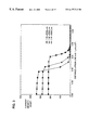
- FIG. 2 is a graph showing the current/voltage characteristics in the forward direction where the radial length w 1 of a anode electrode metal layer in the FWD according to the first embodiment is 3450, 3000, 2500 and 2000 ⁇ m;
- FIG. 3 is a graph showing the relation between the distance from line B—B in the FWD and the current density in a cross section taken along line A—A, where the radial length wi of the anode electrode metal layer in the FWD according to the first embodiment is 3000, 2500, and 2000 ⁇ m;
- FIG. 4 is a graph showing the relation between the distance from line B—B to a free wheel diode and the hole density in the cross section taken along line A—A, where the radial length w 1 of the anode electrode metal layer in the FWD according to the first embodiment is 3000, 2500, and 2000 ⁇ m;
- FIG. 5 is a schematic illustration showing a current path and a part serving as a resistance in the path when a forward bias is applied in the FWD according to the first embodiment
- FIG. 6 is a cross sectional view showing the right half of a symmetrical cross section taken perpendicularly to the electrode surface of an FWD according to a second embodiment of the present invention
- FIG. 7 is an illustration showing an equipotential surface without a field plate in the vicinity of the outer periphery of an anode in the FWD according to the second embodiment
- FIG. 8 is an illustration showing an equipotential surface with a field plate in the vicinity of the out periphery of the anode in the FWD according to the second embodiment
- FIGS. 9 to 15 are cross sections showing the right halves of symmetrical cross sections taken perpendicularly to the electrode surfaces of FWDs according to third to ninth embodiments of the present invention.
- FIG. 16 is a plan view seen from the side of an anode electrode in a conventional FWD
- FIG. 17 is a cross sectional view showing the right half of a symmetrical cross section taken perpendicularly to the semiconductor substrate of a conventional FWD;
- FIG. 18 is an illustration showing how an equipotential surface extends outwardly under a field limiting layer
- FIG. 19 is a graph showing the relation between the current density distribution of an anode electrode in a conventional FWD where w 1 is 3450 ⁇ m as in FIG. 17 and the distance from line B—B in FIG. 1 to the outermost circumference of metal layer 8 for anode electrode;
- FIG. 21 is an illustration showing a field limiting innermost circumferential layer when the radius of curvature is large
- FIG. 22 is an illustration showing the field limiting innermost circumferential layer when the radius of curvature is small
- FIG. 23 is an illustration showing an anode layer and a field limiting innermost circumferential layer with a small overlapping area
- FIG. 24 is an illustration showing an anode layer and a field limiting innermost circumferential layer with a large overlapping area
- FIG. 25 is an illustration showing an equipotential surface when the width of the bottom of the field limiting innermost circumferential layer is small
- FIG. 26 is an illustration showing an equipotential surface when the width of the bottom of the field limiting innermost circumferential layer is large;
- FIG. 27 is a schematic diagram showing a half bridge circuit having an FWD build therein
- FIG. 28 is a waveform chart showing the waveform of the power supply of an IGBT
- FIG. 29 is a waveform chart showing a node 0 -node 1 current/voltage loss, when the IGBT is switched from an off state to an on state in the half bridge circuit having the FWD shown in FIG. 24 built therein;
- FIG. 30 is a waveform chart showing a node 1 -node 2 current/voltage loss, when the IGBT is switched from an off state to an on state in the half bridge circuit having the FWD shown in FIG. 24 build therein.
- FIG. 1 is a cross sectional view of an FWD taken along line x—x in a plan view of the FWD as shown in FIG. 16 .
- the structure of the FWD according to the first embodiment will be now described.
- a plan view of the FWD according to the present embodiment seen from the surface of the semiconductor substrate is similar to FIG. 16 .
- an n-type semiconductor substrate 1 having a width w 2 of 5600 ⁇ m and a thickness of t of 500 ⁇ m in the cross section shown in FIG.
- a cathode layer 2 there are formed a cathode layer 2 , an n-type impurity diffusion region having a concentration higher than semiconductor substrate 1 , formed from a main surface on the bottom of semiconductor substrate 1 to a prescribed depth, and an anode layer 3 having a width w 3 of 3450 ⁇ m, a p-type impurity diffusion region having a surface concentration of 5 ⁇ 10 16 /cm 3 , formed in a region having a diffusion depth of 6 ⁇ m from the main surface on the top side to an axis about in the center of the plan view in FIG. 16 on the main surface on the top side of semiconductor substrate 1 , in other words, from line B—B in FIG. 1 to a position at a prescribed distance.
- a field limiting innermost circumferential layer 4 an annular p-type impurity diffusion region, formed in the main surface on the top side of semiconductor substrate 1 to two-dimensionally surround anode layer 3 , and having a diffusion depth from the main surface on the top side of semiconductor substrate 1 as large as 10 ⁇ m, a width w 4 of 50 ⁇ m when viewed in a cross section, and a diffusion concentration of 1 ⁇ 10 19 /cm 3 , higher than that of anode layer 3 , such that the diffusion depth is larger than anode layer 3 .
- field limiting layers 5 There are a plurality of field limiting layers 5 , a group of annular p-type impurity diffusion regions, provided at prescribed intervals outside and around field limiting innermost circumferential layer 4 , and having the same concentration as field limiting innermost circumferentail layer 4 , a diffusion depth of 10 ⁇ m and a diffusion concentration of 1 ⁇ 10 19 /cm 3 .
- a stopper channels layer 6 , an n-type impurity diffusion region having a concentration higher than that of semiconductor substrate 1 is provided at the outermost circumference of semiconductor substrate 1 .
- a cathode electrode metal layer 7 composed of gold, provided adjacent to cathode layer 2
- an anode electrode metal layer 8 composed of aluminum, provided adjacent to anode layer 3 .
- the width w 1 of anode electrode metal layer 8 is 3000, 2500, and 2000 ⁇ m, each shorter than the width of anode layer 3 by a prescribed length unlike the conventional cases.
- FIG. 2 The relation between the current density and voltage corresponding to the cases where w 1 is 3000, 2500 and 2000 ⁇ m is given in FIG. 2 .
- FIG. 2 when Wi is smaller, the current density as the same voltage is applied decreases, which degrades the characteristic of a diode.
- Data given in FIG. 3 is represented in a graph showing the relation between the current density distribution where w 1 is 3000, 2500, and 2000 ⁇ m and the distance from line B—B in FIG. 1 to the outermost circumference of anode electrode metal layer 8 .
- Data given in FIG. 4 is represented in a graph showing the relation between the hole density distribution where w 1 is 3000, 2500, and 2000 ⁇ m and the distance of anode electrode metal layer 8 from line B—B in FIG. 1 to the outermost circumference.
- FIGS. 19 and 20 uneven distribution of the current densities as shown in FIGS. 19 and 20 according to the conventional cases is eliminated.
- an outermost circumferential part of anode layer 3 formed from the main surface on the top side of semiconductor substrate 1 to a depth of 6 ⁇ m viewed two-dimensionally serves as a resistance to prevent the passage of current generated under anode electrode metal layer 8 toward field limiting innermost circumferential layer 4 , when a forward bias is applied, in other words, when a positive potential is applied to anode electrode metal layer 8 and a negative potential is applied to cathode electrode metal layer 7 , as can be seen from resistance Ro across path II shown in FIG.
- N A is the impurity concentration of anode layer 3 . According to the above expression, if N A equals 1 ⁇ 10 16 /cm 3 , specific resistance ⁇ p is about 0.2105 ⁇ cm. If the distance from the outermost circumference of anode layer 3 to field limiting innermost circumferential layer 4 is 500 ⁇ m, the resistance value R 0 across path II in FIG. 5 is about 0.1053 ⁇ .
- the density of current passed from the bottom side of field limiting innermost circumferential layer 4 toward cathode layer 2 may be reduced, in other words, the concentration of current may be restrained as compared to the case where anode electrode metal layer 8 is formed large enough to be in direct contact with field limiting innermost circumferential layer 4 .
- FIG. 6 A top view of the FWD according to this embodiment seen from the surface of the semiconductor substrate is identical to the top view shown in FIG. 16.
- a cross section taken along line x—x in the plan view of the FWD as in FIG. 16 is given in FIG. 6 .
- the FWD according to this embodiment includes a semiconductor substrate 1 , a cathode layer 2 , a field limiting innermost circumferential layer 4 , a field limiting layer 5 , a stopper channel layer 6 , a cathode electrode metal layer 7 , and a anode electrode metal layer 8 as is the case with the FWD according to the first embodiment.
- the length of anode layer 3 in the radial direction is short and the portion between anode layer 3 and field limiting innermost circumferential layer 4 is electrically disconnected by the function of n-type semiconductor substrate 1 , while a field plate 16 composed of aluminum is provided on a main surface of semiconductor substrate 1 from the outermost circumference of anode electrode metal layer 8 to the inner surface of field limiting innermost circumferential layer 4 through an insulating layer, unlike the FWD according to the first embodiment.
- the part of semiconductor substrate 1 of n-type remains without being implanted with an impurity between p-type anode layer 3 and field limiting innermost circumferential layer 4 , and semiconductor substrate 1 cuts off current passed from anode layer 3 to field limiting innermost circumferential layer 4 when a forward bias is applied.
- the hole density distribution may be prevented from being locally great under field limiting innermost circumferential layer 4 .
- the density of current passed from the bottom side of field limiting innermost circumferential layer 4 to cathode layer 2 may be reduced. Therefore, the concentration of locally great recovery current passed between cathode layer 2 and field limiting innermost circumferential layer 4 which is caused when a reverse bias is applied may be restrained. As a result, destruction by heat in the vicinity of field limiting innermost circumferential layer 4 caused by a temperature rise in the vicinity by recovery current may be restrained.
- intervals between equipotential surfaces are narrowed between anode layer 3 and field limiting innermost circumferential layer 4 , when a reverse bias is applied, which increases charge and the electric field, while in the presence of field plate 16 as shown in FIG. 8, in the potential applied to anode electrode metal layer 8 , intervals between equipotential surfaces between anode layer 3 and field limiting innermost circumferential layer 4 is large, when a reverse bias is applied, the higher part of the potential is sent outside, which relaxes the concentration of electric field. Thus, the concentration of electric field generated between anode layer 3 and field limiting innermost circumferential layer 4 may be restrained.
- FIG. 9 A top view of FWD according to this embodiment seen from the surface of the semiconductor substrate is almost the same as that in FIG. 16.
- a cross section of FWD taken along line x—x in FIG. 16 is as shown in FIG. 9 .
- the FWD according to this embodiment includes a semiconductor substrate 1 , a cathode layer 2 , a field limiting innermost circumferential layer 4 , a field limiting layer 5 , a stopper channel layer 6 , a cathode electrode metal layer 7 , and an anode electrode metal layer 8 as is the case with the FWD according to the first embodiment.
- the length of anode layer 3 in the radial direction is short, the outermost circumferential part of anode layer 3 and field limiting innermost circumferential layer 4 are not in direct contact, the conduction therebetween is substantially cut off by n-type semiconductor substrate 1 , an insulating film 10 is provided on the surface of semiconductor substrate 1 between the outermost circumferential part of anode layer 3 and field limiting innermost circumferential layer 4 , an interconnection 9 composed of polysilicon is provided to cover insulating film 10 , and the portion between the outermost circumferential part of anode layer 3 and field limiting innermost circumferential layer 4 conducts, unlike the FWD according to the first embodiment.
- p-type anode layer 3 and field limiting innermost circumferential layer 4 are provided at an interval defined by n-type semiconductor substrate 1 . Furthermore, since interconnection 9 (a conductive layer) composed of polysilicon to connect anode layer 3 and field limiting innermost circumferential layer 4 is provided on the main surface of semiconductor substrate 1 on the top side through insulating film 10 , an equipotential surfaces having relatively large intervals are formed parallel to the surface of semiconductor substrate 1 and to conductive layer 9 such that electric fields are concentrated between anode layer 3 and field limiting innermost circumferential layer 4 .
- FIG. 10 A top view of the FWD according to this embodiment seen from the surface of the semiconductor substrate is substantially the same as the top view in FIG. 16.
- a cross section taken along line x—x in the top view of the FWD as shown in FIG. 16 is given in FIG. 10 .
- the FWD according to this embodiment includes a semiconductor substrate 1 , a cathode layer 2 , a field limiting innermost circumferential layer 4 , a field limiting layer 5 , a stopper channel layer 6 , a cathode electrode metal layer 7 , and an anode electrode metal layer 8 as is the case with the FWD according to the first embodiment.
- the FWD according to this embodiment includes an n-type impurity diffusion region 11 having a shallower implantation depth than that of anode layer 3 from the outermost circumference of anode layer 3 to the inner surface of field limiting innermost circumferential layer 4 , unlike the FWD according to the first embodiment.
- the p-type part of anode layer 3 having a low concentration immediately under n-type impurity diffusion region 11 serves as a resistance layer between anode layer 3 and field limiting innermost circumferential layer 4 .
- the p-type part of anode layer 3 having low concentration immediately under n-type impurity diffusion region 11 serves as a resistance against current passed from anode layer 3 to field limiting innermost circumferential layer 4 . Therefore, as compared to the case in which only anode layer 3 is provided in the absence of impurity diffusion region 11 , the density of current passed from the bottom side of field limiting innermost circumferential layer 4 toward cathode layer 2 when a forward bias is applied may be reduced.
- the concentration of locally great recovery current passed between cathode layer 2 and field limiting innermost circumferential layer 4 caused when a reverse bias is applied may be restrained. Consequently, destruction by heat in the vicinity of field limiting innermost circumferential layer 4 caused by a temperature rise in the vicinity by recovery current may be restrained.
- FIG. 11 A top view of the FWD according to this embodiment seen from the surface of the semiconductor substrate is substantially the same as that in FIG. 16.
- a cross section taken along line x—x in the plan view of the FWD as shown in FIG. 16 is given in FIG. 11 .
- the FWD according to this embodiment includes a semiconductor substrate 1 , a cathode layer 2 , an anode layer 3 , a field limiting innermost circumferential layer 4 , a field limiting layer 5 , a stopper channel layer 6 , and a cathode electrode metal layer 7 as is the case with the FWD according to the first embodiment.
- anode electrode metal layer 8 extends up to the outermost circumference of anode layer 3 , and there is provided an oxide film 12 formed to fill a trench at the boundary part of anode layer 3 and field limiting innermost circumferential layer 4 , unlike the FWD according to the first embodiment.
- insulating layer 12 filled within the trench is formed between anode layer 3 and field limiting innermost circumferential layer 4 , insulating 12 insulates against current passed from anode layer 3 to field limiting innermost circumferential layer 4 , in other words, cuts off current.
- a forward bias when a forward bias is applied, the density of current passed from the bottom of field limiting innermost circumferential layer 4 toward cathode layer 2 may be reduced.
- the concentration of locally great recovery current passed when a reverse bias is applied may be restrained. Consequently, destruction by heat in the vicinity of field limiting innermost circumferential layer 4 caused by a temperature rise in the vicinity by recovery current may be restrained.
- oxide film 12 filled within the trench may effectively serve as a resistance
- current passed from anode electrode metal layer 8 toward cathode electrode metal layer 7 may be evenly distributed in the width-wise direction as the voltage applied across the region between the anode electrode metal layer 8 and cathode layer 2 is the same.
- the current/voltage characteristics between anode electrode metal layer 8 and cathode electrode metal layer 7 may be improved.
- FIG. 12 A top view of the FWD according to this embodiment seen from the surface of the semiconductor substrate is the same as that in FIG. 16.
- a cross section taken along line x—x in the top view of the FWD as shown in FIG. 16 is given in FIG. 12 .
- the FWD according to this embodiment includes a semiconductor substrate 1 , a cathode layer 2 , a field limiting innermost circumferential layer 4 , a field limiting layer 5 , a stopper channel 6 , and a cathode electrode metal layer 7 as is the case with the FWD according to the first embodiment.
- anode layer 3 in the radial direction is short, a p-type impurity diffusion region 13 having a depth approximately equal to the depth of anode layer 3 from the main surface and a relatively low concentration is provided between anode layer 3 and field limiting innermost circumferential layer 4 .
- Anode electrode metal layer 8 is provided up to the inner side of field limiting innermost circumferential layer 4 , unlike the FWD according to the first embodiment.
- impurity diffusion region 13 having a relatively low concentration is formed between anode layer 3 and field limiting innermost circumferential layer 4 , when a forward bias is applied, impurity diffusion region 13 serves as a resistance against current passed from anode layer 3 to field limiting innermost circumferential layer 4 .
- impurity diffusion region 13 serves as a resistance against current passed from anode layer 3 to field limiting innermost circumferential layer 4 .
- the density of current passed from the bottom side of field limiting innermost circumferential layer 4 to cathode layer 2 may be reduced. Therefore, the concentration of locally great recovery current generated between cathode layer 2 and field limiting innermost circumferential layer 4 when a reverse bias is applied may be restrained. As a result, destruction by heat in the vicinity of field limiting innermost circumferential layer 4 caused by a temperature rise in the vicinity by recovery current may be restrained.
- FIG. 13 A top view of the FWD according to this embodiment seen from the surface of the semiconductor substrate is the same as that in FIG. 16.
- a cross section taken along line x—x in the top view of the FWD as shown in FIG. 16 is as given in FIG. 13 .
- the FWD according to this embodiment includes a semiconductor substrate 1 , a cathode layer 2 , a field limiting innermost circumferential layer 4 , a field limiting layer 5 , a stopper channel layer 6 , a cathode electrode metal layer 7 , and a anode electrode metal layer 8 , as is the case with the FWD according to the first embodiment.
- the FWD according to this embodiment includes a plurality of p-type impurity diffusion regions 14 of a relatively low concentration at prescribed intervals in anode layer 3 from the center toward the outermost peripheral part.
- impurity diffusion regions 14 of the relatively low concentration is formed in anode layer 3 , when a forward bias is applied, impurity diffusion regions 14 serve as a resistance against current passed from anode layer 3 to field limiting innermost circumferential layer 4 .
- the density of current passed from the bottom side of field limiting innermost circumferential layer 4 toward cathode layer 2 may be reduced.
- the concentration of locally great recovery current passed between cathode layer 2 and field limiting innermost circumferential layer 4 may be restrained. Consequently, destruction by heat in the vicinity of field limiting innermost circumferential layer 4 caused by a temperature rise in the vicinity may be restrained.
- anode electrode metal layer 8 is formed about as large as anode layer 3 , p-type impurity diffusion region 14 of the relatively low concentration may effectively serve as a resistance, and current passed from anode electrode metal layer 8 to cathode layer metal layer 7 may be distributed evenly in the width-wise direction of semiconductor substrate 1 while the voltage applied across the region between anode electrode metal layer 8 and cathode electrode metal layer 7 is the same. As a result, the current/voltage characteristic between anode electrode metal layer 8 and cathode electrode metal layer 7 may be improved.
- FIG. 14 A plan view of the FWD according to this embodiment seen from the surface of the semiconductor substrate is the same as that in FIG. 16.
- a cross section taken along line x—x in the plan view of the FWD as shown in FIG. 16 is given in FIG. 14 .
- the FWD according to this embodiment includes a semiconductor substrate 1 , a cathode layer 2 , a field limiting innermost circumferential layer 4 , a field limiting layer 5 , a stopper channel layer 6 , and a cathode electrode metal layer 7 as is the case with the FWD according to the first embodiment.
- the length of anode layer 3 in the radial direction is short, and a p-type impurity diffusion region 15 of a relatively low concentration and having a depth from the main surface shallower than anode layer 3 is provided between anode layer 3 and field limiting innermost circumferential layer 4 .
- anode electrode metal layer 8 is provided up to the inner side surface of field limiting innermost circumferential layer 4 , unlike the FWD according to the first embodiment.
- p-type impurity diffusion region 15 of the relatively low concentration and having a depth smaller than anode layer 3 is formed between anode layer 3 and field limiting innermost circumferential layer 4 .
- impurity diffusion region 15 hardly allows current from anode layer 3 to field limiting innermost circumferential layer 4 . Therefore, the density of current passed from the bottom of field limiting innermost circumferential layer 4 to cathode layer 2 may be reduced.
- the concentration of locally great recovery current passed between cathode layer 2 and field limiting innermost circumferential layer 4 may be restrained. As a result, destruction by heat in the vicinity of field limiting innermost circumferential layer 4 caused by a temperature rise in the vicinity by recovery current may be restrained.
- anode electrode metal layer 8 is formed up to the vicinity of the inner surface of field limiting innermost circumferential layer 4 , the concentration of electric field between anode layer 3 and field limiting innermost circumferential layer 4 may be restrained.
- FIG. 15 A plan view of the FWD according to this embodiment seen from the surface of the semiconductor substrate is the same as that in FIG. 16.
- a cross section taken along line x—x in the plan view of the FWD as shown in FIG. 16 is given in FIG. 15 .
- the FWD according to this embodiment includes a semiconductor substrate 1 , a cathode layer 2 , and an anode layer 3 , a field limiting layer 5 , a stopper channel layer 6 , and a cathode electrode metal layer 7 as is the case with the first embodiment.
- anode electrode metal layer 8 extends up to the vicinity of the outermost circumference of anode layer 3 , and field limiting innermost circumferential layer 4 is divided into a inner side part 4 a and an outer side 4 b such that a low concentration part is formed in the center, unlike the FWD according to the first embodiment.
- inner side part 4 a and outer side part 4 b have a relatively low concentration part therebetween.
- Inner side part 4 a and outer side part 4 b have a relatively smaller hole density than the case in which inner side part 4 a and outer side 4 b do not have such a relatively low concentration part in the central part in the width-direction but is distributed in a constant concentration.
- the density of current passed from field limiting innermost circumferential layer 4 to cathode electrode 2 when a forward bias is applied is relatively small.
- the concentration of locally great recovery current passed between cathode layer 2 and field limiting innermost circumferential layer 4 may be restrained. Consequently, destruction by heat in the vicinity of the inner side part 4 a and outer side part 4 b of field limiting innermost circumferential layer 4 caused by a temperature rise in the vicinity may be restrained.
- inner side part 4 a and outer side part 4 b have a width and an implantation depth in the deepest part identical to the conventional cases, and equipotential surfaces are the same as the conventional cases, the effect of relaxing the concentration of electric field will not be decreased, unlike the case of reducing the implantation depth to reduce the hole density.
Landscapes
- Engineering & Computer Science (AREA)
- Microelectronics & Electronic Packaging (AREA)
- Power Engineering (AREA)
- Physics & Mathematics (AREA)
- Ceramic Engineering (AREA)
- Condensed Matter Physics & Semiconductors (AREA)
- General Physics & Mathematics (AREA)
- Computer Hardware Design (AREA)
- Electrodes Of Semiconductors (AREA)
- Metal-Oxide And Bipolar Metal-Oxide Semiconductor Integrated Circuits (AREA)
- Thyristors (AREA)
Applications Claiming Priority (2)
| Application Number | Priority Date | Filing Date | Title |
|---|---|---|---|
| JP21389198A JP4017258B2 (ja) | 1998-07-29 | 1998-07-29 | 半導体装置 |
| JP10-213891 | 1998-07-29 |
Publications (1)
| Publication Number | Publication Date |
|---|---|
| US6177713B1 true US6177713B1 (en) | 2001-01-23 |
Family
ID=16646736
Family Applications (1)
| Application Number | Title | Priority Date | Filing Date |
|---|---|---|---|
| US09/241,088 Expired - Lifetime US6177713B1 (en) | 1998-07-29 | 1999-02-01 | Free wheel diode for preventing destruction of a field limiting innermost circumferential layer |
Country Status (4)
| Country | Link |
|---|---|
| US (1) | US6177713B1 (ja) |
| JP (1) | JP4017258B2 (ja) |
| KR (1) | KR100326222B1 (ja) |
| DE (1) | DE19908477B4 (ja) |
Cited By (16)
| Publication number | Priority date | Publication date | Assignee | Title |
|---|---|---|---|---|
| US20060170075A1 (en) * | 2005-01-28 | 2006-08-03 | Mitsubishi Denki Kabushiki Kaisha | Semiconductor device |
| US7400017B2 (en) | 2004-04-28 | 2008-07-15 | Mitsubishi Denki Kabushiki Kaisha | Reverse conducting semiconductor device and a fabrication method thereof |
| CN102290433A (zh) * | 2010-06-18 | 2011-12-21 | 赛米控电子股份有限公司 | 具有两级掺杂曲线的功率半导体器件 |
| US8102025B2 (en) | 2006-02-24 | 2012-01-24 | Denso Corporation | Semiconductor device having IGBT and diode |
| CN102683427A (zh) * | 2011-03-09 | 2012-09-19 | 三菱电机株式会社 | 半导体器件及其制造方法 |
| US20120319163A1 (en) * | 2011-06-15 | 2012-12-20 | Denso Corporation | Semiconductor device including insulated gate bipolar transistor and diode |
| CN102983077A (zh) * | 2012-12-06 | 2013-03-20 | 乐山嘉洋科技发展有限公司 | 一种二极管芯片的制备方法 |
| US20130075877A1 (en) * | 2011-09-27 | 2013-03-28 | Denso Corporation | Semiconductor device having lateral element |
| US20140091359A1 (en) * | 2012-10-02 | 2014-04-03 | Mitsubishi Electric Corporation | Semiconductor device |
| US20150194482A1 (en) * | 2009-04-06 | 2015-07-09 | Mitsubishi Electric Corporation | Semiconductor device and method for fabricating the same |
| US20160087110A1 (en) * | 2013-07-08 | 2016-03-24 | Miitsubishi Electric Corporation | Semiconductor device |
| US20160260703A1 (en) * | 2014-01-29 | 2016-09-08 | Mitsubishi Electric Corporation | Power semiconductor device |
| US9450110B2 (en) | 2013-03-21 | 2016-09-20 | Fuji Electric Co., Ltd. | Semiconductor device |
| US20170110596A1 (en) * | 2015-01-14 | 2017-04-20 | Fuji Electric Co., Ltd. | Semiconductor device |
| US10784255B2 (en) | 2014-06-27 | 2020-09-22 | Robert Bosch Gmbh | Diode having a plate-shaped semiconductor element |
| EP4246588A1 (en) * | 2022-03-16 | 2023-09-20 | Huawei Digital Power Technologies Co., Ltd. | Diode and power circuit |
Families Citing this family (6)
| Publication number | Priority date | Publication date | Assignee | Title |
|---|---|---|---|---|
| JP4761644B2 (ja) * | 2001-04-18 | 2011-08-31 | 三菱電機株式会社 | 半導体装置 |
| KR100538876B1 (ko) * | 2001-09-04 | 2005-12-23 | 엘지전자 주식회사 | 패킷 교환기와 패킷 관문 교환기간의 링크 채널 관리 방법 |
| KR100485131B1 (ko) * | 2002-10-18 | 2005-04-25 | 재단법인서울대학교산학협력재단 | 반도체 소자의 접합 마감 구조 |
| KR200482243Y1 (ko) | 2012-08-20 | 2017-01-04 | 갈원홍 | 이동 가능한 대용량의 저장탱크 |
| KR102291424B1 (ko) | 2019-05-30 | 2021-08-20 | 갈원홍 | 악취 제거장치 및 그것을 구비한 가축분뇨 저장설비 |
| JP7257912B2 (ja) * | 2019-08-01 | 2023-04-14 | 三菱電機株式会社 | 半導体装置 |
Citations (10)
| Publication number | Priority date | Publication date | Assignee | Title |
|---|---|---|---|---|
| JPS58151068A (ja) * | 1982-03-02 | 1983-09-08 | Toshiba Corp | 高耐圧半導体装置 |
| JPS59150471A (ja) * | 1983-01-31 | 1984-08-28 | Toshiba Corp | 半導体装置 |
| US4587547A (en) * | 1979-05-07 | 1986-05-06 | Nippon Telegraph & Telephone Public Corp. | Electrode structure for a semiconductor devices |
| US4602266A (en) * | 1983-01-28 | 1986-07-22 | U.S. Philips Corporation | High voltage guard ring with variable width shallow portion |
| JPH0191475A (ja) | 1987-10-02 | 1989-04-11 | Toyota Autom Loom Works Ltd | pn接合ダイオード |
| JPH03222475A (ja) * | 1990-01-29 | 1991-10-01 | Matsushita Electron Corp | 半導体装置 |
| JPH04364079A (ja) | 1991-06-11 | 1992-12-16 | Fuji Electric Co Ltd | 半導体装置 |
| JPH07249737A (ja) | 1994-03-11 | 1995-09-26 | Mitsubishi Electric Corp | プレーナ型半導体装置およびその製造方法 |
| US5552625A (en) * | 1993-03-10 | 1996-09-03 | Hitachi, Ltd. | Semiconductor device having a semi-insulating layer |
| US5969400A (en) * | 1995-03-15 | 1999-10-19 | Kabushiki Kaisha Toshiba | High withstand voltage semiconductor device |
Family Cites Families (3)
| Publication number | Priority date | Publication date | Assignee | Title |
|---|---|---|---|---|
| DE3832732A1 (de) * | 1988-09-27 | 1990-03-29 | Asea Brown Boveri | Leistungshalbleiterdiode |
| JP3522887B2 (ja) * | 1995-04-20 | 2004-04-26 | 株式会社東芝 | 高耐圧半導体素子 |
| JP3447884B2 (ja) * | 1995-03-15 | 2003-09-16 | 株式会社東芝 | 高耐圧半導体素子 |
-
1998
- 1998-07-29 JP JP21389198A patent/JP4017258B2/ja not_active Expired - Lifetime
-
1999
- 1999-02-01 US US09/241,088 patent/US6177713B1/en not_active Expired - Lifetime
- 1999-02-26 DE DE19908477A patent/DE19908477B4/de not_active Expired - Lifetime
- 1999-04-10 KR KR1019990012710A patent/KR100326222B1/ko not_active IP Right Cessation
Patent Citations (10)
| Publication number | Priority date | Publication date | Assignee | Title |
|---|---|---|---|---|
| US4587547A (en) * | 1979-05-07 | 1986-05-06 | Nippon Telegraph & Telephone Public Corp. | Electrode structure for a semiconductor devices |
| JPS58151068A (ja) * | 1982-03-02 | 1983-09-08 | Toshiba Corp | 高耐圧半導体装置 |
| US4602266A (en) * | 1983-01-28 | 1986-07-22 | U.S. Philips Corporation | High voltage guard ring with variable width shallow portion |
| JPS59150471A (ja) * | 1983-01-31 | 1984-08-28 | Toshiba Corp | 半導体装置 |
| JPH0191475A (ja) | 1987-10-02 | 1989-04-11 | Toyota Autom Loom Works Ltd | pn接合ダイオード |
| JPH03222475A (ja) * | 1990-01-29 | 1991-10-01 | Matsushita Electron Corp | 半導体装置 |
| JPH04364079A (ja) | 1991-06-11 | 1992-12-16 | Fuji Electric Co Ltd | 半導体装置 |
| US5552625A (en) * | 1993-03-10 | 1996-09-03 | Hitachi, Ltd. | Semiconductor device having a semi-insulating layer |
| JPH07249737A (ja) | 1994-03-11 | 1995-09-26 | Mitsubishi Electric Corp | プレーナ型半導体装置およびその製造方法 |
| US5969400A (en) * | 1995-03-15 | 1999-10-19 | Kabushiki Kaisha Toshiba | High withstand voltage semiconductor device |
Non-Patent Citations (2)
| Title |
|---|
| "3.3 kV IGBT Modules having Soft Recovery Diodes with High Reverse Recovery di/dt Capability (HiRC)", M. Nagasu et al., PCIM Inter '98 Japan Procceedings, pp. 175-178. |
| "Improvement of the Diode Characteristics Using Emitter-Controlled Principles (EMCON-Diode)", A. Porst et al., 1997 IEEE, pp. 213-216. |
Cited By (34)
| Publication number | Priority date | Publication date | Assignee | Title |
|---|---|---|---|---|
| US7400017B2 (en) | 2004-04-28 | 2008-07-15 | Mitsubishi Denki Kabushiki Kaisha | Reverse conducting semiconductor device and a fabrication method thereof |
| US7491982B2 (en) | 2005-01-28 | 2009-02-17 | Mitsubishi Denki Kabushiki Kaisha | Diode having low forward voltage drop |
| US20060170075A1 (en) * | 2005-01-28 | 2006-08-03 | Mitsubishi Denki Kabushiki Kaisha | Semiconductor device |
| US8102025B2 (en) | 2006-02-24 | 2012-01-24 | Denso Corporation | Semiconductor device having IGBT and diode |
| DE102007008568B4 (de) * | 2006-02-24 | 2012-11-08 | Denso Corporation | Halbleitervorrichtung mit IGBT und Diode |
| DE102007008568B8 (de) * | 2006-02-24 | 2013-01-17 | Denso Corporation | Halbleitervorrichtung mit IGBT und Diode |
| US9741788B2 (en) * | 2009-04-06 | 2017-08-22 | Mitsubishi Electric Corporation | Semiconductor device and method for fabricating the same |
| US20150194482A1 (en) * | 2009-04-06 | 2015-07-09 | Mitsubishi Electric Corporation | Semiconductor device and method for fabricating the same |
| EP2398057A3 (de) * | 2010-06-18 | 2013-05-22 | SEMIKRON Elektronik GmbH | Leistungshalbleiterbauelement mit zweistufigem Dotierungsprofil |
| CN102290433A (zh) * | 2010-06-18 | 2011-12-21 | 赛米控电子股份有限公司 | 具有两级掺杂曲线的功率半导体器件 |
| CN102290433B (zh) * | 2010-06-18 | 2016-04-13 | 赛米控电子股份有限公司 | 具有两级掺杂曲线的功率半导体器件 |
| CN102683427B (zh) * | 2011-03-09 | 2015-08-05 | 三菱电机株式会社 | 半导体器件及其制造方法 |
| US9202936B2 (en) | 2011-03-09 | 2015-12-01 | Mitsubishi Electric Corporation | Semiconductor device |
| CN102683427A (zh) * | 2011-03-09 | 2012-09-19 | 三菱电机株式会社 | 半导体器件及其制造方法 |
| US8841699B2 (en) * | 2011-06-15 | 2014-09-23 | Denso Corporation | Semiconductor device including insulated gate bipolar transistor and diode |
| US20120319163A1 (en) * | 2011-06-15 | 2012-12-20 | Denso Corporation | Semiconductor device including insulated gate bipolar transistor and diode |
| US9136362B2 (en) * | 2011-09-27 | 2015-09-15 | Denso Corporation | Semiconductor device having lateral element |
| US20130075877A1 (en) * | 2011-09-27 | 2013-03-28 | Denso Corporation | Semiconductor device having lateral element |
| CN103715273A (zh) * | 2012-10-02 | 2014-04-09 | 三菱电机株式会社 | 半导体装置 |
| US9257541B2 (en) * | 2012-10-02 | 2016-02-09 | Mitsubishi Electric Corporation | High-breakdown-voltage power semiconductor device having a diode |
| US20140091359A1 (en) * | 2012-10-02 | 2014-04-03 | Mitsubishi Electric Corporation | Semiconductor device |
| CN103715273B (zh) * | 2012-10-02 | 2016-08-31 | 三菱电机株式会社 | 半导体装置 |
| DE102013219499B4 (de) | 2012-10-02 | 2020-07-09 | Mitsubishi Electric Corporation | Halbleitervorrichtung |
| CN102983077B (zh) * | 2012-12-06 | 2015-10-14 | 乐山嘉洋科技发展有限公司 | 一种二极管芯片的制备方法 |
| CN102983077A (zh) * | 2012-12-06 | 2013-03-20 | 乐山嘉洋科技发展有限公司 | 一种二极管芯片的制备方法 |
| US9450110B2 (en) | 2013-03-21 | 2016-09-20 | Fuji Electric Co., Ltd. | Semiconductor device |
| US20160087110A1 (en) * | 2013-07-08 | 2016-03-24 | Miitsubishi Electric Corporation | Semiconductor device |
| US9455355B2 (en) * | 2013-07-08 | 2016-09-27 | Mitsubishi Electric Corporation | Semiconductor device |
| US9941269B2 (en) * | 2014-01-29 | 2018-04-10 | Mitsubishi Electric Corporation | Power semiconductor device including well extension region and field-limiting rings |
| US20160260703A1 (en) * | 2014-01-29 | 2016-09-08 | Mitsubishi Electric Corporation | Power semiconductor device |
| US10784255B2 (en) | 2014-06-27 | 2020-09-22 | Robert Bosch Gmbh | Diode having a plate-shaped semiconductor element |
| US20170110596A1 (en) * | 2015-01-14 | 2017-04-20 | Fuji Electric Co., Ltd. | Semiconductor device |
| US10056501B2 (en) * | 2015-01-14 | 2018-08-21 | Fuji Electric Co., Ltd. | Power diode with improved reverse-recovery immunity |
| EP4246588A1 (en) * | 2022-03-16 | 2023-09-20 | Huawei Digital Power Technologies Co., Ltd. | Diode and power circuit |
Also Published As
| Publication number | Publication date |
|---|---|
| DE19908477A1 (de) | 2000-02-10 |
| JP2000049360A (ja) | 2000-02-18 |
| KR100326222B1 (ko) | 2002-02-27 |
| DE19908477B4 (de) | 2007-06-14 |
| JP4017258B2 (ja) | 2007-12-05 |
| KR20000011235A (ko) | 2000-02-25 |
Similar Documents
| Publication | Publication Date | Title |
|---|---|---|
| US6177713B1 (en) | Free wheel diode for preventing destruction of a field limiting innermost circumferential layer | |
| US6667515B2 (en) | High breakdown voltage semiconductor device | |
| US4789882A (en) | High power MOSFET with direct connection from connection pads to underlying silicon | |
| US8716826B2 (en) | Semiconductor device | |
| JP3288115B2 (ja) | 半導体部品 | |
| US5191395A (en) | Mos type semiconductor device with means to prevent parasitic bipolar transistor | |
| US7301178B2 (en) | Pressed-contact type semiconductor device | |
| US11145714B2 (en) | Semiconductor device | |
| JP2000277726A (ja) | 高耐圧半導体素子 | |
| JPH09283754A (ja) | 高耐圧半導体装置 | |
| US7135718B2 (en) | Diode device and transistor device | |
| JPH07115189A (ja) | 絶縁ゲート型バイポーラトランジスタ | |
| US7598587B2 (en) | Semiconductor device | |
| KR100397882B1 (ko) | 전계효과-제어가능반도체소자 | |
| JP2862027B2 (ja) | 絶縁ゲート型バイポーラトランジスタ | |
| US5079607A (en) | Mos type semiconductor device | |
| US4982245A (en) | Compound diode assembly of reduced leakage current | |
| US6423598B1 (en) | Semiconductor device, a method of manufacturing the same, and a semiconductor device protective circuit | |
| JPS6182477A (ja) | 導電変調型mosfet | |
| JP2970774B2 (ja) | 半導体デバイス | |
| KR100316040B1 (ko) | 반도체 장치 및 그 제조 방법 | |
| EP0110320A1 (en) | A MOS transistor | |
| JP4062373B2 (ja) | Mos・バイポーラ複合型の半導体装置およびmos型の半導体装置 | |
| JP3297087B2 (ja) | 高耐圧半導体装置 | |
| JP3216315B2 (ja) | 絶縁ゲート型バイポーラトランジスタ |
Legal Events
| Date | Code | Title | Description |
|---|---|---|---|
| AS | Assignment |
Owner name: MITSUBISHI DENKI KABUSHIKI KAISHA, JAPAN Free format text: ASSIGNMENT OF ASSIGNORS INTEREST;ASSIGNORS:AONO, SHINJI;HARADA, MASANA;REEL/FRAME:009744/0017 Effective date: 19990121 |
|
| FEPP | Fee payment procedure |
Free format text: PAYOR NUMBER ASSIGNED (ORIGINAL EVENT CODE: ASPN); ENTITY STATUS OF PATENT OWNER: LARGE ENTITY |
|
| STCF | Information on status: patent grant |
Free format text: PATENTED CASE |
|
| FPAY | Fee payment |
Year of fee payment: 4 |
|
| FPAY | Fee payment |
Year of fee payment: 8 |
|
| FPAY | Fee payment |
Year of fee payment: 12 |